EP1636842B1 - Dispositif semi-conducteur empilable et procede de sa fabrication - Google Patents
Dispositif semi-conducteur empilable et procede de sa fabrication Download PDFInfo
- Publication number
- EP1636842B1 EP1636842B1 EP04735511A EP04735511A EP1636842B1 EP 1636842 B1 EP1636842 B1 EP 1636842B1 EP 04735511 A EP04735511 A EP 04735511A EP 04735511 A EP04735511 A EP 04735511A EP 1636842 B1 EP1636842 B1 EP 1636842B1
- Authority
- EP
- European Patent Office
- Prior art keywords
- interconnections
- insulating film
- semiconductor
- interconnection
- base plate
- Prior art date
- Legal status (The legal status is an assumption and is not a legal conclusion. Google has not performed a legal analysis and makes no representation as to the accuracy of the status listed.)
- Expired - Fee Related
Links
Images


Classifications
-
- H—ELECTRICITY
- H01—ELECTRIC ELEMENTS
- H01L—SEMICONDUCTOR DEVICES NOT COVERED BY CLASS H10
- H01L23/00—Details of semiconductor or other solid state devices
- H01L23/52—Arrangements for conducting electric current within the device in operation from one component to another, i.e. interconnections, e.g. wires, lead frames
- H01L23/538—Arrangements for conducting electric current within the device in operation from one component to another, i.e. interconnections, e.g. wires, lead frames the interconnection structure between a plurality of semiconductor chips being formed on, or in, insulating substrates
-
- H—ELECTRICITY
- H01—ELECTRIC ELEMENTS
- H01L—SEMICONDUCTOR DEVICES NOT COVERED BY CLASS H10
- H01L24/00—Arrangements for connecting or disconnecting semiconductor or solid-state bodies; Methods or apparatus related thereto
- H01L24/80—Methods for connecting semiconductor or other solid state bodies using means for bonding being attached to, or being formed on, the surface to be connected
- H01L24/83—Methods for connecting semiconductor or other solid state bodies using means for bonding being attached to, or being formed on, the surface to be connected using a layer connector
-
- H—ELECTRICITY
- H01—ELECTRIC ELEMENTS
- H01L—SEMICONDUCTOR DEVICES NOT COVERED BY CLASS H10
- H01L23/00—Details of semiconductor or other solid state devices
- H01L23/52—Arrangements for conducting electric current within the device in operation from one component to another, i.e. interconnections, e.g. wires, lead frames
- H01L23/538—Arrangements for conducting electric current within the device in operation from one component to another, i.e. interconnections, e.g. wires, lead frames the interconnection structure between a plurality of semiconductor chips being formed on, or in, insulating substrates
- H01L23/5389—Arrangements for conducting electric current within the device in operation from one component to another, i.e. interconnections, e.g. wires, lead frames the interconnection structure between a plurality of semiconductor chips being formed on, or in, insulating substrates the chips being integrally enclosed by the interconnect and support structures
-
- H—ELECTRICITY
- H01—ELECTRIC ELEMENTS
- H01L—SEMICONDUCTOR DEVICES NOT COVERED BY CLASS H10
- H01L24/00—Arrangements for connecting or disconnecting semiconductor or solid-state bodies; Methods or apparatus related thereto
- H01L24/01—Means for bonding being attached to, or being formed on, the surface to be connected, e.g. chip-to-package, die-attach, "first-level" interconnects; Manufacturing methods related thereto
- H01L24/18—High density interconnect [HDI] connectors; Manufacturing methods related thereto
- H01L24/19—Manufacturing methods of high density interconnect preforms
-
- H—ELECTRICITY
- H01—ELECTRIC ELEMENTS
- H01L—SEMICONDUCTOR DEVICES NOT COVERED BY CLASS H10
- H01L24/00—Arrangements for connecting or disconnecting semiconductor or solid-state bodies; Methods or apparatus related thereto
- H01L24/01—Means for bonding being attached to, or being formed on, the surface to be connected, e.g. chip-to-package, die-attach, "first-level" interconnects; Manufacturing methods related thereto
- H01L24/26—Layer connectors, e.g. plate connectors, solder or adhesive layers; Manufacturing methods related thereto
- H01L24/27—Manufacturing methods
-
- H—ELECTRICITY
- H01—ELECTRIC ELEMENTS
- H01L—SEMICONDUCTOR DEVICES NOT COVERED BY CLASS H10
- H01L24/00—Arrangements for connecting or disconnecting semiconductor or solid-state bodies; Methods or apparatus related thereto
- H01L24/01—Means for bonding being attached to, or being formed on, the surface to be connected, e.g. chip-to-package, die-attach, "first-level" interconnects; Manufacturing methods related thereto
- H01L24/26—Layer connectors, e.g. plate connectors, solder or adhesive layers; Manufacturing methods related thereto
- H01L24/28—Structure, shape, material or disposition of the layer connectors prior to the connecting process
- H01L24/29—Structure, shape, material or disposition of the layer connectors prior to the connecting process of an individual layer connector
-
- H—ELECTRICITY
- H01—ELECTRIC ELEMENTS
- H01L—SEMICONDUCTOR DEVICES NOT COVERED BY CLASS H10
- H01L24/00—Arrangements for connecting or disconnecting semiconductor or solid-state bodies; Methods or apparatus related thereto
- H01L24/93—Batch processes
- H01L24/95—Batch processes at chip-level, i.e. with connecting carried out on a plurality of singulated devices, i.e. on diced chips
- H01L24/97—Batch processes at chip-level, i.e. with connecting carried out on a plurality of singulated devices, i.e. on diced chips the devices being connected to a common substrate, e.g. interposer, said common substrate being separable into individual assemblies after connecting
-
- H—ELECTRICITY
- H01—ELECTRIC ELEMENTS
- H01L—SEMICONDUCTOR DEVICES NOT COVERED BY CLASS H10
- H01L25/00—Assemblies consisting of a plurality of individual semiconductor or other solid state devices ; Multistep manufacturing processes thereof
- H01L25/03—Assemblies consisting of a plurality of individual semiconductor or other solid state devices ; Multistep manufacturing processes thereof all the devices being of a type provided for in the same subgroup of groups H01L27/00 - H01L33/00, or in a single subclass of H10K, H10N, e.g. assemblies of rectifier diodes
- H01L25/10—Assemblies consisting of a plurality of individual semiconductor or other solid state devices ; Multistep manufacturing processes thereof all the devices being of a type provided for in the same subgroup of groups H01L27/00 - H01L33/00, or in a single subclass of H10K, H10N, e.g. assemblies of rectifier diodes the devices having separate containers
- H01L25/105—Assemblies consisting of a plurality of individual semiconductor or other solid state devices ; Multistep manufacturing processes thereof all the devices being of a type provided for in the same subgroup of groups H01L27/00 - H01L33/00, or in a single subclass of H10K, H10N, e.g. assemblies of rectifier diodes the devices having separate containers the devices being of a type provided for in group H01L27/00
-
- H—ELECTRICITY
- H01—ELECTRIC ELEMENTS
- H01L—SEMICONDUCTOR DEVICES NOT COVERED BY CLASS H10
- H01L2223/00—Details relating to semiconductor or other solid state devices covered by the group H01L23/00
- H01L2223/58—Structural electrical arrangements for semiconductor devices not otherwise provided for
- H01L2223/64—Impedance arrangements
- H01L2223/66—High-frequency adaptations
- H01L2223/6661—High-frequency adaptations for passive devices
- H01L2223/6677—High-frequency adaptations for passive devices for antenna, e.g. antenna included within housing of semiconductor device
-
- H—ELECTRICITY
- H01—ELECTRIC ELEMENTS
- H01L—SEMICONDUCTOR DEVICES NOT COVERED BY CLASS H10
- H01L2224/00—Indexing scheme for arrangements for connecting or disconnecting semiconductor or solid-state bodies and methods related thereto as covered by H01L24/00
- H01L2224/01—Means for bonding being attached to, or being formed on, the surface to be connected, e.g. chip-to-package, die-attach, "first-level" interconnects; Manufacturing methods related thereto
- H01L2224/02—Bonding areas; Manufacturing methods related thereto
- H01L2224/023—Redistribution layers [RDL] for bonding areas
-
- H—ELECTRICITY
- H01—ELECTRIC ELEMENTS
- H01L—SEMICONDUCTOR DEVICES NOT COVERED BY CLASS H10
- H01L2224/00—Indexing scheme for arrangements for connecting or disconnecting semiconductor or solid-state bodies and methods related thereto as covered by H01L24/00
- H01L2224/01—Means for bonding being attached to, or being formed on, the surface to be connected, e.g. chip-to-package, die-attach, "first-level" interconnects; Manufacturing methods related thereto
- H01L2224/02—Bonding areas; Manufacturing methods related thereto
- H01L2224/04—Structure, shape, material or disposition of the bonding areas prior to the connecting process
- H01L2224/0401—Bonding areas specifically adapted for bump connectors, e.g. under bump metallisation [UBM]
-
- H—ELECTRICITY
- H01—ELECTRIC ELEMENTS
- H01L—SEMICONDUCTOR DEVICES NOT COVERED BY CLASS H10
- H01L2224/00—Indexing scheme for arrangements for connecting or disconnecting semiconductor or solid-state bodies and methods related thereto as covered by H01L24/00
- H01L2224/01—Means for bonding being attached to, or being formed on, the surface to be connected, e.g. chip-to-package, die-attach, "first-level" interconnects; Manufacturing methods related thereto
- H01L2224/02—Bonding areas; Manufacturing methods related thereto
- H01L2224/04—Structure, shape, material or disposition of the bonding areas prior to the connecting process
- H01L2224/04105—Bonding areas formed on an encapsulation of the semiconductor or solid-state body, e.g. bonding areas on chip-scale packages
-
- H—ELECTRICITY
- H01—ELECTRIC ELEMENTS
- H01L—SEMICONDUCTOR DEVICES NOT COVERED BY CLASS H10
- H01L2224/00—Indexing scheme for arrangements for connecting or disconnecting semiconductor or solid-state bodies and methods related thereto as covered by H01L24/00
- H01L2224/01—Means for bonding being attached to, or being formed on, the surface to be connected, e.g. chip-to-package, die-attach, "first-level" interconnects; Manufacturing methods related thereto
- H01L2224/10—Bump connectors; Manufacturing methods related thereto
- H01L2224/11—Manufacturing methods
- H01L2224/1147—Manufacturing methods using a lift-off mask
-
- H—ELECTRICITY
- H01—ELECTRIC ELEMENTS
- H01L—SEMICONDUCTOR DEVICES NOT COVERED BY CLASS H10
- H01L2224/00—Indexing scheme for arrangements for connecting or disconnecting semiconductor or solid-state bodies and methods related thereto as covered by H01L24/00
- H01L2224/01—Means for bonding being attached to, or being formed on, the surface to be connected, e.g. chip-to-package, die-attach, "first-level" interconnects; Manufacturing methods related thereto
- H01L2224/10—Bump connectors; Manufacturing methods related thereto
- H01L2224/12—Structure, shape, material or disposition of the bump connectors prior to the connecting process
- H01L2224/12105—Bump connectors formed on an encapsulation of the semiconductor or solid-state body, e.g. bumps on chip-scale packages
-
- H—ELECTRICITY
- H01—ELECTRIC ELEMENTS
- H01L—SEMICONDUCTOR DEVICES NOT COVERED BY CLASS H10
- H01L2224/00—Indexing scheme for arrangements for connecting or disconnecting semiconductor or solid-state bodies and methods related thereto as covered by H01L24/00
- H01L2224/01—Means for bonding being attached to, or being formed on, the surface to be connected, e.g. chip-to-package, die-attach, "first-level" interconnects; Manufacturing methods related thereto
- H01L2224/18—High density interconnect [HDI] connectors; Manufacturing methods related thereto
- H01L2224/20—Structure, shape, material or disposition of high density interconnect preforms
- H01L2224/21—Structure, shape, material or disposition of high density interconnect preforms of an individual HDI interconnect
- H01L2224/211—Disposition
-
- H—ELECTRICITY
- H01—ELECTRIC ELEMENTS
- H01L—SEMICONDUCTOR DEVICES NOT COVERED BY CLASS H10
- H01L2224/00—Indexing scheme for arrangements for connecting or disconnecting semiconductor or solid-state bodies and methods related thereto as covered by H01L24/00
- H01L2224/01—Means for bonding being attached to, or being formed on, the surface to be connected, e.g. chip-to-package, die-attach, "first-level" interconnects; Manufacturing methods related thereto
- H01L2224/26—Layer connectors, e.g. plate connectors, solder or adhesive layers; Manufacturing methods related thereto
- H01L2224/27—Manufacturing methods
- H01L2224/274—Manufacturing methods by blanket deposition of the material of the layer connector
-
- H—ELECTRICITY
- H01—ELECTRIC ELEMENTS
- H01L—SEMICONDUCTOR DEVICES NOT COVERED BY CLASS H10
- H01L2224/00—Indexing scheme for arrangements for connecting or disconnecting semiconductor or solid-state bodies and methods related thereto as covered by H01L24/00
- H01L2224/01—Means for bonding being attached to, or being formed on, the surface to be connected, e.g. chip-to-package, die-attach, "first-level" interconnects; Manufacturing methods related thereto
- H01L2224/26—Layer connectors, e.g. plate connectors, solder or adhesive layers; Manufacturing methods related thereto
- H01L2224/28—Structure, shape, material or disposition of the layer connectors prior to the connecting process
- H01L2224/29—Structure, shape, material or disposition of the layer connectors prior to the connecting process of an individual layer connector
- H01L2224/29001—Core members of the layer connector
- H01L2224/29099—Material
- H01L2224/2919—Material with a principal constituent of the material being a polymer, e.g. polyester, phenolic based polymer, epoxy
-
- H—ELECTRICITY
- H01—ELECTRIC ELEMENTS
- H01L—SEMICONDUCTOR DEVICES NOT COVERED BY CLASS H10
- H01L2224/00—Indexing scheme for arrangements for connecting or disconnecting semiconductor or solid-state bodies and methods related thereto as covered by H01L24/00
- H01L2224/01—Means for bonding being attached to, or being formed on, the surface to be connected, e.g. chip-to-package, die-attach, "first-level" interconnects; Manufacturing methods related thereto
- H01L2224/26—Layer connectors, e.g. plate connectors, solder or adhesive layers; Manufacturing methods related thereto
- H01L2224/31—Structure, shape, material or disposition of the layer connectors after the connecting process
- H01L2224/32—Structure, shape, material or disposition of the layer connectors after the connecting process of an individual layer connector
- H01L2224/321—Disposition
- H01L2224/32151—Disposition the layer connector connecting between a semiconductor or solid-state body and an item not being a semiconductor or solid-state body, e.g. chip-to-substrate, chip-to-passive
- H01L2224/32221—Disposition the layer connector connecting between a semiconductor or solid-state body and an item not being a semiconductor or solid-state body, e.g. chip-to-substrate, chip-to-passive the body and the item being stacked
- H01L2224/32225—Disposition the layer connector connecting between a semiconductor or solid-state body and an item not being a semiconductor or solid-state body, e.g. chip-to-substrate, chip-to-passive the body and the item being stacked the item being non-metallic, e.g. insulating substrate with or without metallisation
-
- H—ELECTRICITY
- H01—ELECTRIC ELEMENTS
- H01L—SEMICONDUCTOR DEVICES NOT COVERED BY CLASS H10
- H01L2224/00—Indexing scheme for arrangements for connecting or disconnecting semiconductor or solid-state bodies and methods related thereto as covered by H01L24/00
- H01L2224/73—Means for bonding being of different types provided for in two or more of groups H01L2224/10, H01L2224/18, H01L2224/26, H01L2224/34, H01L2224/42, H01L2224/50, H01L2224/63, H01L2224/71
- H01L2224/732—Location after the connecting process
- H01L2224/73251—Location after the connecting process on different surfaces
- H01L2224/73267—Layer and HDI connectors
-
- H—ELECTRICITY
- H01—ELECTRIC ELEMENTS
- H01L—SEMICONDUCTOR DEVICES NOT COVERED BY CLASS H10
- H01L2224/00—Indexing scheme for arrangements for connecting or disconnecting semiconductor or solid-state bodies and methods related thereto as covered by H01L24/00
- H01L2224/80—Methods for connecting semiconductor or other solid state bodies using means for bonding being attached to, or being formed on, the surface to be connected
- H01L2224/83—Methods for connecting semiconductor or other solid state bodies using means for bonding being attached to, or being formed on, the surface to be connected using a layer connector
- H01L2224/8319—Arrangement of the layer connectors prior to mounting
- H01L2224/83191—Arrangement of the layer connectors prior to mounting wherein the layer connectors are disposed only on the semiconductor or solid-state body
-
- H—ELECTRICITY
- H01—ELECTRIC ELEMENTS
- H01L—SEMICONDUCTOR DEVICES NOT COVERED BY CLASS H10
- H01L2224/00—Indexing scheme for arrangements for connecting or disconnecting semiconductor or solid-state bodies and methods related thereto as covered by H01L24/00
- H01L2224/80—Methods for connecting semiconductor or other solid state bodies using means for bonding being attached to, or being formed on, the surface to be connected
- H01L2224/83—Methods for connecting semiconductor or other solid state bodies using means for bonding being attached to, or being formed on, the surface to be connected using a layer connector
- H01L2224/838—Bonding techniques
- H01L2224/8385—Bonding techniques using a polymer adhesive, e.g. an adhesive based on silicone, epoxy, polyimide, polyester
- H01L2224/83855—Hardening the adhesive by curing, i.e. thermosetting
- H01L2224/83856—Pre-cured adhesive, i.e. B-stage adhesive
-
- H—ELECTRICITY
- H01—ELECTRIC ELEMENTS
- H01L—SEMICONDUCTOR DEVICES NOT COVERED BY CLASS H10
- H01L2224/00—Indexing scheme for arrangements for connecting or disconnecting semiconductor or solid-state bodies and methods related thereto as covered by H01L24/00
- H01L2224/91—Methods for connecting semiconductor or solid state bodies including different methods provided for in two or more of groups H01L2224/80 - H01L2224/90
- H01L2224/92—Specific sequence of method steps
- H01L2224/922—Connecting different surfaces of the semiconductor or solid-state body with connectors of different types
- H01L2224/9222—Sequential connecting processes
- H01L2224/92242—Sequential connecting processes the first connecting process involving a layer connector
- H01L2224/92244—Sequential connecting processes the first connecting process involving a layer connector the second connecting process involving a build-up interconnect
-
- H—ELECTRICITY
- H01—ELECTRIC ELEMENTS
- H01L—SEMICONDUCTOR DEVICES NOT COVERED BY CLASS H10
- H01L2224/00—Indexing scheme for arrangements for connecting or disconnecting semiconductor or solid-state bodies and methods related thereto as covered by H01L24/00
- H01L2224/93—Batch processes
- H01L2224/95—Batch processes at chip-level, i.e. with connecting carried out on a plurality of singulated devices, i.e. on diced chips
- H01L2224/97—Batch processes at chip-level, i.e. with connecting carried out on a plurality of singulated devices, i.e. on diced chips the devices being connected to a common substrate, e.g. interposer, said common substrate being separable into individual assemblies after connecting
-
- H—ELECTRICITY
- H01—ELECTRIC ELEMENTS
- H01L—SEMICONDUCTOR DEVICES NOT COVERED BY CLASS H10
- H01L2225/00—Details relating to assemblies covered by the group H01L25/00 but not provided for in its subgroups
- H01L2225/03—All the devices being of a type provided for in the same subgroup of groups H01L27/00 - H01L33/648 and H10K99/00
- H01L2225/10—All the devices being of a type provided for in the same subgroup of groups H01L27/00 - H01L33/648 and H10K99/00 the devices having separate containers
- H01L2225/1005—All the devices being of a type provided for in the same subgroup of groups H01L27/00 - H01L33/648 and H10K99/00 the devices having separate containers the devices being of a type provided for in group H01L27/00
- H01L2225/1011—All the devices being of a type provided for in the same subgroup of groups H01L27/00 - H01L33/648 and H10K99/00 the devices having separate containers the devices being of a type provided for in group H01L27/00 the containers being in a stacked arrangement
- H01L2225/1017—All the devices being of a type provided for in the same subgroup of groups H01L27/00 - H01L33/648 and H10K99/00 the devices having separate containers the devices being of a type provided for in group H01L27/00 the containers being in a stacked arrangement the lowermost container comprising a device support
- H01L2225/1035—All the devices being of a type provided for in the same subgroup of groups H01L27/00 - H01L33/648 and H10K99/00 the devices having separate containers the devices being of a type provided for in group H01L27/00 the containers being in a stacked arrangement the lowermost container comprising a device support the device being entirely enclosed by the support, e.g. high-density interconnect [HDI]
-
- H—ELECTRICITY
- H01—ELECTRIC ELEMENTS
- H01L—SEMICONDUCTOR DEVICES NOT COVERED BY CLASS H10
- H01L2225/00—Details relating to assemblies covered by the group H01L25/00 but not provided for in its subgroups
- H01L2225/03—All the devices being of a type provided for in the same subgroup of groups H01L27/00 - H01L33/648 and H10K99/00
- H01L2225/10—All the devices being of a type provided for in the same subgroup of groups H01L27/00 - H01L33/648 and H10K99/00 the devices having separate containers
- H01L2225/1005—All the devices being of a type provided for in the same subgroup of groups H01L27/00 - H01L33/648 and H10K99/00 the devices having separate containers the devices being of a type provided for in group H01L27/00
- H01L2225/1011—All the devices being of a type provided for in the same subgroup of groups H01L27/00 - H01L33/648 and H10K99/00 the devices having separate containers the devices being of a type provided for in group H01L27/00 the containers being in a stacked arrangement
- H01L2225/1047—Details of electrical connections between containers
- H01L2225/1058—Bump or bump-like electrical connections, e.g. balls, pillars, posts
-
- H—ELECTRICITY
- H01—ELECTRIC ELEMENTS
- H01L—SEMICONDUCTOR DEVICES NOT COVERED BY CLASS H10
- H01L2924/00—Indexing scheme for arrangements or methods for connecting or disconnecting semiconductor or solid-state bodies as covered by H01L24/00
- H01L2924/01—Chemical elements
- H01L2924/01005—Boron [B]
-
- H—ELECTRICITY
- H01—ELECTRIC ELEMENTS
- H01L—SEMICONDUCTOR DEVICES NOT COVERED BY CLASS H10
- H01L2924/00—Indexing scheme for arrangements or methods for connecting or disconnecting semiconductor or solid-state bodies as covered by H01L24/00
- H01L2924/01—Chemical elements
- H01L2924/01006—Carbon [C]
-
- H—ELECTRICITY
- H01—ELECTRIC ELEMENTS
- H01L—SEMICONDUCTOR DEVICES NOT COVERED BY CLASS H10
- H01L2924/00—Indexing scheme for arrangements or methods for connecting or disconnecting semiconductor or solid-state bodies as covered by H01L24/00
- H01L2924/01—Chemical elements
- H01L2924/01013—Aluminum [Al]
-
- H—ELECTRICITY
- H01—ELECTRIC ELEMENTS
- H01L—SEMICONDUCTOR DEVICES NOT COVERED BY CLASS H10
- H01L2924/00—Indexing scheme for arrangements or methods for connecting or disconnecting semiconductor or solid-state bodies as covered by H01L24/00
- H01L2924/01—Chemical elements
- H01L2924/01015—Phosphorus [P]
-
- H—ELECTRICITY
- H01—ELECTRIC ELEMENTS
- H01L—SEMICONDUCTOR DEVICES NOT COVERED BY CLASS H10
- H01L2924/00—Indexing scheme for arrangements or methods for connecting or disconnecting semiconductor or solid-state bodies as covered by H01L24/00
- H01L2924/01—Chemical elements
- H01L2924/01027—Cobalt [Co]
-
- H—ELECTRICITY
- H01—ELECTRIC ELEMENTS
- H01L—SEMICONDUCTOR DEVICES NOT COVERED BY CLASS H10
- H01L2924/00—Indexing scheme for arrangements or methods for connecting or disconnecting semiconductor or solid-state bodies as covered by H01L24/00
- H01L2924/01—Chemical elements
- H01L2924/01029—Copper [Cu]
-
- H—ELECTRICITY
- H01—ELECTRIC ELEMENTS
- H01L—SEMICONDUCTOR DEVICES NOT COVERED BY CLASS H10
- H01L2924/00—Indexing scheme for arrangements or methods for connecting or disconnecting semiconductor or solid-state bodies as covered by H01L24/00
- H01L2924/01—Chemical elements
- H01L2924/01033—Arsenic [As]
-
- H—ELECTRICITY
- H01—ELECTRIC ELEMENTS
- H01L—SEMICONDUCTOR DEVICES NOT COVERED BY CLASS H10
- H01L2924/00—Indexing scheme for arrangements or methods for connecting or disconnecting semiconductor or solid-state bodies as covered by H01L24/00
- H01L2924/01—Chemical elements
- H01L2924/01047—Silver [Ag]
-
- H—ELECTRICITY
- H01—ELECTRIC ELEMENTS
- H01L—SEMICONDUCTOR DEVICES NOT COVERED BY CLASS H10
- H01L2924/00—Indexing scheme for arrangements or methods for connecting or disconnecting semiconductor or solid-state bodies as covered by H01L24/00
- H01L2924/01—Chemical elements
- H01L2924/01074—Tungsten [W]
-
- H—ELECTRICITY
- H01—ELECTRIC ELEMENTS
- H01L—SEMICONDUCTOR DEVICES NOT COVERED BY CLASS H10
- H01L2924/00—Indexing scheme for arrangements or methods for connecting or disconnecting semiconductor or solid-state bodies as covered by H01L24/00
- H01L2924/01—Chemical elements
- H01L2924/01078—Platinum [Pt]
-
- H—ELECTRICITY
- H01—ELECTRIC ELEMENTS
- H01L—SEMICONDUCTOR DEVICES NOT COVERED BY CLASS H10
- H01L2924/00—Indexing scheme for arrangements or methods for connecting or disconnecting semiconductor or solid-state bodies as covered by H01L24/00
- H01L2924/01—Chemical elements
- H01L2924/01082—Lead [Pb]
-
- H—ELECTRICITY
- H01—ELECTRIC ELEMENTS
- H01L—SEMICONDUCTOR DEVICES NOT COVERED BY CLASS H10
- H01L2924/00—Indexing scheme for arrangements or methods for connecting or disconnecting semiconductor or solid-state bodies as covered by H01L24/00
- H01L2924/013—Alloys
- H01L2924/014—Solder alloys
-
- H—ELECTRICITY
- H01—ELECTRIC ELEMENTS
- H01L—SEMICONDUCTOR DEVICES NOT COVERED BY CLASS H10
- H01L2924/00—Indexing scheme for arrangements or methods for connecting or disconnecting semiconductor or solid-state bodies as covered by H01L24/00
- H01L2924/06—Polymers
- H01L2924/0665—Epoxy resin
-
- H—ELECTRICITY
- H01—ELECTRIC ELEMENTS
- H01L—SEMICONDUCTOR DEVICES NOT COVERED BY CLASS H10
- H01L2924/00—Indexing scheme for arrangements or methods for connecting or disconnecting semiconductor or solid-state bodies as covered by H01L24/00
- H01L2924/06—Polymers
- H01L2924/078—Adhesive characteristics other than chemical
- H01L2924/07802—Adhesive characteristics other than chemical not being an ohmic electrical conductor
-
- H—ELECTRICITY
- H01—ELECTRIC ELEMENTS
- H01L—SEMICONDUCTOR DEVICES NOT COVERED BY CLASS H10
- H01L2924/00—Indexing scheme for arrangements or methods for connecting or disconnecting semiconductor or solid-state bodies as covered by H01L24/00
- H01L2924/095—Indexing scheme for arrangements or methods for connecting or disconnecting semiconductor or solid-state bodies as covered by H01L24/00 with a principal constituent of the material being a combination of two or more materials provided in the groups H01L2924/013 - H01L2924/0715
- H01L2924/097—Glass-ceramics, e.g. devitrified glass
- H01L2924/09701—Low temperature co-fired ceramic [LTCC]
-
- H—ELECTRICITY
- H01—ELECTRIC ELEMENTS
- H01L—SEMICONDUCTOR DEVICES NOT COVERED BY CLASS H10
- H01L2924/00—Indexing scheme for arrangements or methods for connecting or disconnecting semiconductor or solid-state bodies as covered by H01L24/00
- H01L2924/10—Details of semiconductor or other solid state devices to be connected
- H01L2924/11—Device type
- H01L2924/12—Passive devices, e.g. 2 terminal devices
- H01L2924/1204—Optical Diode
- H01L2924/12042—LASER
-
- H—ELECTRICITY
- H01—ELECTRIC ELEMENTS
- H01L—SEMICONDUCTOR DEVICES NOT COVERED BY CLASS H10
- H01L2924/00—Indexing scheme for arrangements or methods for connecting or disconnecting semiconductor or solid-state bodies as covered by H01L24/00
- H01L2924/10—Details of semiconductor or other solid state devices to be connected
- H01L2924/11—Device type
- H01L2924/14—Integrated circuits
-
- H—ELECTRICITY
- H01—ELECTRIC ELEMENTS
- H01L—SEMICONDUCTOR DEVICES NOT COVERED BY CLASS H10
- H01L2924/00—Indexing scheme for arrangements or methods for connecting or disconnecting semiconductor or solid-state bodies as covered by H01L24/00
- H01L2924/15—Details of package parts other than the semiconductor or other solid state devices to be connected
- H01L2924/151—Die mounting substrate
- H01L2924/153—Connection portion
- H01L2924/1531—Connection portion the connection portion being formed only on the surface of the substrate opposite to the die mounting surface
- H01L2924/15311—Connection portion the connection portion being formed only on the surface of the substrate opposite to the die mounting surface being a ball array, e.g. BGA
-
- H—ELECTRICITY
- H01—ELECTRIC ELEMENTS
- H01L—SEMICONDUCTOR DEVICES NOT COVERED BY CLASS H10
- H01L2924/00—Indexing scheme for arrangements or methods for connecting or disconnecting semiconductor or solid-state bodies as covered by H01L24/00
- H01L2924/15—Details of package parts other than the semiconductor or other solid state devices to be connected
- H01L2924/151—Die mounting substrate
- H01L2924/153—Connection portion
- H01L2924/1532—Connection portion the connection portion being formed on the die mounting surface of the substrate
- H01L2924/1533—Connection portion the connection portion being formed on the die mounting surface of the substrate the connection portion being formed both on the die mounting surface of the substrate and outside the die mounting surface of the substrate
- H01L2924/15331—Connection portion the connection portion being formed on the die mounting surface of the substrate the connection portion being formed both on the die mounting surface of the substrate and outside the die mounting surface of the substrate being a ball array, e.g. BGA
-
- H—ELECTRICITY
- H01—ELECTRIC ELEMENTS
- H01L—SEMICONDUCTOR DEVICES NOT COVERED BY CLASS H10
- H01L2924/00—Indexing scheme for arrangements or methods for connecting or disconnecting semiconductor or solid-state bodies as covered by H01L24/00
- H01L2924/19—Details of hybrid assemblies other than the semiconductor or other solid state devices to be connected
- H01L2924/1901—Structure
- H01L2924/1904—Component type
- H01L2924/19041—Component type being a capacitor
-
- H—ELECTRICITY
- H01—ELECTRIC ELEMENTS
- H01L—SEMICONDUCTOR DEVICES NOT COVERED BY CLASS H10
- H01L2924/00—Indexing scheme for arrangements or methods for connecting or disconnecting semiconductor or solid-state bodies as covered by H01L24/00
- H01L2924/19—Details of hybrid assemblies other than the semiconductor or other solid state devices to be connected
- H01L2924/1901—Structure
- H01L2924/1904—Component type
- H01L2924/19042—Component type being an inductor
-
- H—ELECTRICITY
- H01—ELECTRIC ELEMENTS
- H01L—SEMICONDUCTOR DEVICES NOT COVERED BY CLASS H10
- H01L2924/00—Indexing scheme for arrangements or methods for connecting or disconnecting semiconductor or solid-state bodies as covered by H01L24/00
- H01L2924/19—Details of hybrid assemblies other than the semiconductor or other solid state devices to be connected
- H01L2924/1901—Structure
- H01L2924/1904—Component type
- H01L2924/19043—Component type being a resistor
-
- H—ELECTRICITY
- H01—ELECTRIC ELEMENTS
- H01L—SEMICONDUCTOR DEVICES NOT COVERED BY CLASS H10
- H01L2924/00—Indexing scheme for arrangements or methods for connecting or disconnecting semiconductor or solid-state bodies as covered by H01L24/00
- H01L2924/30—Technical effects
- H01L2924/301—Electrical effects
- H01L2924/30105—Capacitance
-
- H—ELECTRICITY
- H01—ELECTRIC ELEMENTS
- H01L—SEMICONDUCTOR DEVICES NOT COVERED BY CLASS H10
- H01L2924/00—Indexing scheme for arrangements or methods for connecting or disconnecting semiconductor or solid-state bodies as covered by H01L24/00
- H01L2924/30—Technical effects
- H01L2924/301—Electrical effects
- H01L2924/3011—Impedance
Definitions
- the present invention relates to a semiconductor package having a semiconductor constructing body and a method of manufacturing the same.
- CSPs Chip size Packages
- JP 2001274034 discloses an electronic parts package comprising electronic parts packed at a high density and shielding the electronic parts from electromagnetic noise.
- US 5 875 100 relates to a high-density mounting method for an electronic circuit board.
- a passivation film (insulating film) is formed on the upper surface of a semiconductor substrate having an integrated circuit and a plurality of connection pads for external connection. Opening portions are formed in the passivation film in correspondence with the connection pads. Interconnections to be connected to the connection pads through the opening portions are formed.
- An external connection electrode made of, e.g., a columnar electrode is formed on the side of the other end portion of each interconnection. The space between the external connection electrodes is filled with a sealing material.
- the device when solder balls are formed on the external connection electrodes, the device can be bonded to a circuit board with connection terminals by the face-down method.
- the mounting area can be almost the same as the size of the bare semiconductor package.
- the CSP can therefore greatly decrease the sizes of electronic devices as compared to the conventional face-up bonding method using wire bonding.
- the conventional semiconductor package raises the following problems when the number of connection pads increases as the degree of integration becomes higher.
- a CSP normally has external connection electrodes arrayed in a matrix on the upper surface of a semiconductor substrate.
- this array is used for a semiconductor substrate having many external connection electrodes, the size and pitch of the external connection electrodes become small. Because of this disadvantage, the CSP technology can hardly be applied to devices which have a large number of external connection electrodes relative to the size of the semiconductor substrate. More specifically, if the external connection electrodes have small size and pitch, alignment for connection to the circuit board becomes difficult, and the cost of connection to the circuit board increases.
- the device can be bonded to a circuit board by the face-down method, and the mounting area can be almost the same as the size of the semiconductor substrate.
- the sizes of electronic devices can greatly be reduced as compared to the conventional face-up bonding method using wire bonding.
- this method has a limitation on size reduction. More specifically, when other necessary circuit elements such as an inductor circuit element and antenna circuit element are formed on the circuit board, and the conventional semiconductor substrate is connected to these circuit elements to obtain a desired circuit function, the semiconductor substrate and circuit elements are arranged two-dimensionally. Hence, size reduction is limited.
- the wiring length increases. This may increase the impedance (stray capacitance or the like), resulting in degradation in circuit characteristics.
- connection terminals for external connection can have necessary size and pitch. Hence, the reliability of connection to a circuit board can be increased.
- an electronic component using the semiconductor package can be made compact.
- the wiring length between circuit elements can be decreased, the circuit characteristics can be improved.
- the arrangement region of the connection terminal portions having projecting electrodes used for external connection can be made larger than the size of the semiconductor constructing body. Even when the number of connection pads of the semiconductor constructing body increases, the decrease in size and pitch of the connection terminal portions can be suppressed while ensuring a necessary size. Hence, the reliability of connection to a circuit board can be increased.
- an electronic component or a thin-film circuit element can be mounted on the semiconductor package, or a plurality of semiconductor packages can be stacked on each other. Since an electronic component or a thin-film circuit element can integrally be mounted on the semiconductor constructing body, or a plurality of semiconductor constructing bodies can be mounted at a high density, size reduction of an electronic device using this semiconductor package can be promoted. In addition, since the wiring length between the semiconductor constructing body and a thin-film circuit element or electronic component or between the semiconductor constructing bodies can be decreased, the circuit characteristics can be improved.
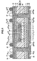
- FIG. 1 is a sectional view showing a semiconductor package according to a first example, useful for understanding the present invention.
- This semiconductor package has a base plate 1 having a rectangular planar shape.
- the base plate 1 is made of an insulating material prepared by impregnating glass fibers, aramid fibers, or liquid crystal fibers with epoxy resin, polyimide resin, BT (Bismaleimide Triazine) resin, or PPE (PolyPhenylene Ether).
- the base plate 1 may made of an insulating material such as silicon, glass, ceramic, or a single resin.
- the lower surface of a semiconductor constructing body 2 which has a rectangular planar shape and is slightly smaller than the base plate 1 is bonded to the central portion of the upper surface (one surface) of the base plate 1 via an adhesive layer 3 made of a die bonding material.
- the semiconductor constructing body 2 has interconnections, columnar electrodes, and a sealing film (to be described later) and is generally called a CSP.
- the semiconductor constructing body 2 is also particularly called a wafer-level CSP (W-CSP) because a method of forming the interconnections, columnar electrodes, and sealing film on a silicon wafer and then executing dicing to obtain individual semiconductor constructing bodies 2 is employed, as will be described later.
- W-CSP wafer-level CSP
- the structure of the semiconductor constructing body 2 will be described below.
- the semiconductor constructing body 2 has a silicon substrate (semiconductor substrate) 4.
- the silicon substrate 4 is bonded to the base plate 1 via the adhesive layer 3.
- An integrated circuit having a predetermined function is formed at the central portion of the upper surface of the silicon substrate 4.
- a plurality of connection pads 5 are formed at the peripheral portion on the upper surface.
- the connection pads 5 are made of an aluminum-based metal and electrically connected to the integrated circuit.
- An insulating film 6 made of silicon oxide is formed on the upper surface of the silicon substrate 4 and the connection pads 5 except the central portion of each connection pad 5. The central portion of each connection pad 5 is exposed through an opening portion 7 formed in the insulating film 6.
- a protective film (insulating film) 8 made of epoxy resin or polyimide resin is formed on the upper surface of the insulating film 6.
- opening portions 9 are formed in the protective film 8 at positions corresponding to the opening portions 7 of the insulating film 6.
- An underlying metal layer 10 made of copper extends from the upper surface of each connection pad 5 exposed through the opening portions 7 and 9 to a predetermined portion on the upper surface of the protective film 8.
- Interconnections 11 made of copper are formed on the entire upper surfaces of the underlying metal layers 10, respectively.
- a columnar electrode (external connection electrode) 12 made of copper is formed on the upper surface of the connection pad portion of each interconnection 11.
- a sealing film (insulating film) 13 made of epoxy resin or polyimide resin is formed around the columnar electrodes 12 and on the upper surface of the protective film 8 including the interconnections 11. The upper surface of the sealing film 13 is flush with those of the columnar electrodes 12.
- the semiconductor constructing body 2 called a W-CSP includes the silicon substrate 4, connection pads 5, and insulating film 6 and also includes the protective film 8, interconnections 11, columnar electrodes 12, and sealing film 13.
- An insulating layer 14 having a rectangular frame shape is formed on the upper surface of the base plate 1 around the semiconductor constructing body 2.
- the upper surface of the insulating layer 14 is substantially flush with that of the semiconductor constructing body 2.
- the insulating layer 14 is made of, e.g., a thermosetting resin or a material prepared by dispersing a reinforcing material such as glass fibers or silica fillers in a thermosetting resin.
- a first upper insulating film 15 having a flat upper surface is formed on the upper surfaces of the semiconductor constructing body 2 and insulating layer 14.
- the first upper insulating film 15 is normally called a build-up material which is used for a build-up substrate.
- the first upper insulating film 15 is made of, e.g., a thermosetting resin such as epoxy resin or BT resin containing reinforcing materials such as fibers or fillers.
- the fiber is glass fiber or aramid fiber.
- the filler is silica filler or ceramic filler.
- Upper underlying metal layers 16 made of copper are formed at predetermined portions on the upper surface of the first upper insulating film 15.
- An upper interconnection 17 made of copper is formed on the entire upper surface of each upper underlying metal layer 16. At least some of the upper underlying metal layers 16 including the upper interconnections 17 are electrically connected to the upper surfaces of the columnar electrodes 12 through opening portions 18 formed in the first upper insulating film 15 at portions corresponding to the central portions of the upper surfaces of the columnar electrodes 12.
- a second upper insulating film 19 made of solder resist is formed on the upper surfaces of the first upper insulating films 15 and the upper interconnections 17.
- An opening portion 20 is formed in the second upper insulating film 19 at a portion corresponding to the connection terminal portion of each upper interconnection 17.
- a solder ball 21 is formed in and above each opening portion 20 and electrically connected to the connection terminal portion of the upper interconnection 17.
- the plurality of solder balls 21 are arranged in a matrix on the second upper insulating film 19.
- a first lower insulating film 22 having a flat lower surface is formed on the lower surface (other surface) of the base plate 1.
- the first lower insulating film 22 is made of, e.g., the same material as the first upper insulating film 15.
- Lower underlying metal layers 23 made of copper are formed at predetermined positions on the lower surface of the first lower insulating film 22.
- a lower interconnection 24 made of copper is formed on the entire lower surface of each lower underlying metal layer 23.
- a second lower insulating film 25 made of solder resist is formed on the lower surfaces of the first lower insulating film 22 and the lower interconnections 24.
- An opening portion 26 is formed in the lower insulating film 25 at a portion corresponding to the connection terminal portion of each lower interconnection 24.
- each of the portions 28 includes an underlying metal layer 28a made of copper and a copper layer 28b, which is formed on the inner surface of a through hole 27.
- a cavity is formed in the copper layer 28b.
- the cavity may be filled with a conductive material 29 such as copper paste, silver paste, or a conductive resin.
- the cavity portion may be filled with an insulating resin so as to increase the reliability by preventing invasion of any external impurities such as water into the semiconductor package.
- the size of the base plate 1 is larger than that of the semiconductor constructing body 2 to some extent. Accordingly, the arrangement region of the connection terminal portions of the upper interconnections 17 can be made larger than the size of the semiconductor constructing body 2 to some extent. Hence, the size and pitch of the connection terminal portions of the upper interconnections 17 (the portions in the opening portions 20 of the second upper insulating film 19) can be made larger than those of the columnar electrodes 12.
- connection terminal portions of the upper interconnections 17 arranged in a matrix are arranged not only on a region corresponding to the semiconductor constructing body 2 but also on a region corresponding to the insulating layer 14 arranged outside the outer side surface of the semiconductor constructing body 2.
- solder balls 21 arranged in a matrix on the second upper insulating film 19 at least the solder balls 21 at the outermost positions are arranged around the semiconductor constructing body 2.
- the lower interconnections 24 are formed under the first lower insulating films 22 formed under the base plate 1.
- the lower interconnections 24 are connected to at least some of the upper interconnections 17 through the vertical conducting portions 28 formed in the through holes 27 formed in the first upper insulating film 15, insulating layer 14, base plate 1, and first lower insulating film 22.
- thin-film circuit elements such as capacitor circuit elements, inductor circuit elements, or antenna circuit elements may be formed by at least some of the lower interconnections 24.
- the thin-film circuit elements may be connected to the upper interconnections 17 through the vertical conducting portions 28.
- chip components such as capacitors or resistors or electronic components such as IC chips may be mounted on the upper surface of the second lower insulating film 25.
- chip components such as capacitors or resistors or electronic components such as IC chips
- the circuit characteristics can be improved.
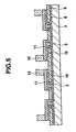
- FIG. 2 is a sectional view showing an example of a method of manufacturing the semiconductor constructing body applied to the semiconductor package according to the first example.
- connection pads 5 made of an aluminum-based metal, the insulating film 6 made of silicon oxide, and the protective film 8 made of epoxy resin or polyimide resin are formed on the silicon substrate (semiconductor substrate) 4 in a wafer state.
- the central portions of the connection pads 5 are exposed through the opening portions 7 and 9 formed in the insulating film 6 and protective film 8.
- an integrated circuit having a predetermined function is formed in a region of each of the silicon substrates 4 in the wafer state, where each semiconductor constructing body should be formed.
- Each connection pad 5 is electrically connected to the integrated circuit formed in a corresponding region.
- the underlying metal layer 10 is formed on the entire upper surface of the protective film 8, including the upper surfaces of the connection pads 5 exposed through the opening portions 7 and 9.
- the underlying metal layer 10 may have only a copper layer formed by electroless plating or only a copper layer formed by sputtering.
- a copper layer may be formed by sputtering on a thin titanium layer formed by sputtering.
- a plating resist film 31 is formed on the upper surface of the underlying metal layer 10 and then patterned.
- the plating resist film 31 has an opening portion 32 at a position corresponding to the formation region of each interconnection 11.
- Copper electroplating is executed using the underlying metal layer 10 as a plating current path to form the interconnection 11 on the upper surface of the underlying metal layer 10 in each opening portion 32 of the plating resist film 31. Then, the plating resist film 31 is removed.
- a plating resist film 33 formed and then patterned on the upper surface of the underlying metal layer 10 including the interconnections 11.
- the plating resist film 33 has an opening portion 34 at a position corresponding to the formation region of each columnar electrode 12. Copper electroplating is executed using the underlying metal layer 10 as a plating current path to form the columnar electrode 12 on the upper surface of the connection pad portion of the interconnection 11 in each opening portion 34 of the plating resist film 33. Thereafter, the plating resist film 33 is removed. Unnecessary portions of the underlying metal layer 10 are removed by etching using the interconnections 11 as a mask so that the underlying metal layers 10 are left only under the interconnections 11, as shown in FIG. 5 .
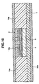
- the sealing film 13 made of epoxy resin or polyimide resin is formed on the entire upper surface of the protective film 8 including the columnar electrodes 12 and interconnections 11 by screen printing, spin coating, or die coating such that the film thickness is more than the height of the columnar electrodes 12. Hence, in this state, the upper surfaces of the columnar electrodes 12 are covered with the sealing film 13.
- the upper surfaces of the sealing film 13 and columnar electrodes 12 are appropriately polished to expose the upper surfaces of the columnar electrodes 12, as shown in FIG. 7 .
- the upper surface of the sealing film 13 including the exposed upper surfaces of the columnar electrodes 12 is also planarized.
- the reason why the upper surface side of the columnar electrodes 12 is appropriately polished is that the heights of the columnar electrodes 12 formed by electroplating have a variation and need to be uniformed by canceling the variation.
- the adhesive layer 3 is bonded to the entire lower surface of the silicon substrate 4.
- the adhesive layer 3 is made of a die bonding material such as epoxy resin or polyimide resin and sticks to the silicon substrate 4 in a semi-set state by heating and pressing.
- the adhesive layer 3 sticking to the silicon substrate 4 is bonded to a dicing tape.
- the respective structures are peeled from the dicing tape. Accordingly, a plurality of semiconductor constructing bodies 2 each having the adhesive layer 3 on the lower surface of the silicon substrate 4, as shown in FIG. 1 , are obtained.
- the adhesive layer 3 exists on the lower surface of the silicon substrate 4.
- the very cumbersome operation for forming an adhesive layer on the lower surface of the silicon substrate 4 of each semiconductor constructing body 2 after the dicing step is unnecessary.
- the operation for peeling each semiconductor constructing body from the dicing tape after the dicing step is much simpler than the operation for forming an adhesive layer on the lower surface of the silicon substrate 4 of each semiconductor constructing body 2 after the dicing step.
- FIG. 10 is a sectional view showing an example of a method of manufacturing the semiconductor package according to this example.
- the base plate 1 is prepared.
- the base plate 1 is so large that a plurality of base plates 1 shown in FIG. 1 can be sampled.
- the base plate 1 has a rectangular planar shape, though its shape is not limited.
- the adhesive layers 3 bonded to the lower surfaces of the silicon substrates 4 of the semiconductor constructing bodies 2 are bonded to a plurality of predetermined portions on the upper surface (one surface) of the base plate 1. In this bonding process, the adhesive layer 3 is finally set by heating and pressing.
- a first insulating material 14a is formed on the upper surface of the base plate 1 between the semiconductor constructing bodies 2 and outside those arranged at the outermost positions by, e.g., screen printing or spin coating.
- a sheet-shaped second insulating material 15a is placed on the upper surface of the first insulating material 14a.
- the first insulating material 14a is made of, e.g., a thermosetting resin or a material prepared by dispersing a reinforcing material such as glass fibers or silica fillers in a thermosetting resin.
- the sheet-shaped second and third insulating materials 15a and 22a are not limited to but is preferably made of a build-up material.
- a thermosetting resin such as epoxy resin or BT resin, which is mixed with a silica filler and semi-set, can be used.
- a sheet-shaped prepreg material prepared by semi-setting a thermosetting resin or a material containing no filler but only a thermosetting resin may be used.
- the first to third insulating materials 14a, 15a, and 22a are heated and pressed by using a pair of heating/pressing plates 37 and 38 shown in FIG. 11 . Accordingly, the insulating layer 14 is formed on the upper surface of the base plate 1 between the semiconductor constructing bodies 2 and outside those arranged at the outermost positions.
- the first upper insulating film 15 is formed on the upper surfaces of the semiconductor constructing bodies 2 and insulating layer 14.
- the first lower insulating film 22 is formed on the lower surface of the base plate 1.
- the upper surface of the first upper insulating film 15 is pressed by the lower surface of the upper heating/pressing plate 37 and therefore becomes flat.
- the upper surface of the first lower insulating film 22 is pressed by the upper surface of the lower heating/pressing plate 38 and therefore becomes flat.
- no polishing step is necessary for planarizing the upper surface of the first upper insulating film 15 and that of the first lower insulating film 22.
- the base plate 1 is relatively large and has a size of, e.g., 500 X 500 mm, the upper surfaces of the first upper insulating film 15 and first lower insulating film 22 for the plurality of semiconductor constructing bodies 2 arranged on the base plate 1 can easily be planarized at once.
- the opening portions 18 are formed in the first upper insulating film 15 at portions corresponding to the central portions of the upper surfaces of the columnar electrodes 12 by, e.g., laser machining for irradiating the structure with a laser beam.
- the through holes 27 are formed in the first upper insulating film 15, insulating layer 14, base plate 1, and first lower insulating film 22 at predetermined positions by using a mechanical drill or laser machining for irradiating the structure with a CO 2 laser beam. Epoxy smears generated in the opening portions 18 and through holes 27 are removed by a desmearing process, as needed.
- the upper underlying metal layer 16, lower underlying metal layer 23, and underlying metal layer 28a are formed by copper electroless plating on the entire upper surface of the first upper insulating film 15 including the upper surfaces of the columnar electrodes 12 exposed through the opening portions 18, the entire upper surface of the first lower insulating film 22, and on the inner surfaces of the through holes 27.
- the upper interconnections 17 and lower interconnections 24 are formed on the upper surface of the upper underlying metal layer 16 and the upper surface of the lower underlying metal layer 23, respectively, by patterning plating. More specifically, an upper plating resist film 41 is formed and then patterned on the upper surface of the upper underlying metal layer 16. A lower plating resist film 42 is also formed and then patterned on the upper surface of the lower underlying metal layer 23. In this case, opening portions 43 are formed in the upper plating resist film 41 at portions corresponding to the formation regions of the upper interconnections 17 including the through holes 27. In addition, opening portions 44 are formed in the lower plating resist film 42 at portions corresponding to the formation regions of the lower interconnections 24 including the through holes 27.
- Copper electroplating is executed by using the upper underlying metal layer 16, lower underlying metal layer 23, and underlying metal layer 28a as a plating current path. Accordingly, the upper interconnections 17 are formed on the upper surfaces of the upper underlying metal layer 16 in the opening portions 43 of the upper plating resist film 41. The lower interconnections 24 are formed on the upper surfaces of the lower underlying metal layer 23 in the opening portions 44 of the lower plating resist film 42. Furthermore, the copper layers 28b are formed on the surfaces of the underlying metal layers 28a in the through holes 27.
- the plating resist films 41 and 42 are removed. Unnecessary portions of the underlying metal layers 16 and 23 are removed by etching using the upper inter-connections 17 and lower interconnections 24 as a mask. As shown in FIG. 14 , the upper underlying metal layers 16 are left only under the upper interconnections 17. In addition, the lower underlying metal layers 23 are left only on the lower interconnection 24. In this state, at least some of the upper underlying metal layers 16 including the upper interconnections 17 are connected to the upper surfaces of the columnar electrodes 12 through the opening portions 18 of the first upper insulating film 15.
- At least some of the upper underlying metal layers 16 including the upper interconnections 17 and the lower underlying metal layers 23 including the lower interconnections 24 are connected through the vertical conducting portions 28 each including the underlying metal layer 28a and copper layer 28b, which are formed on the inner surface of the through hole 27.
- each vertical conducting portion 28 is filled with the conductive material 29 such as copper paste, silver paste, or a conductive resin by screen printing.
- the extra conductive material 29 projecting from each through hole 27 is removed by buffing, as needed.
- the second upper insulating film 19 made of solder resist is formed on the upper surface of the first upper insulating film 15 including the upper interconnections 17 by screen printing or spin coating.
- the opening portions 20 are formed in the second upper insulating film 19 at portions corresponding to the connection pad portions of the upper interconnections 17.
- the second lower insulating film 25 made of solder resist is formed on the upper surface of the first lower insulating film 22 including the lower interconnections 24 by screen printing or spin coating.
- the opening portions 26 are formed in the second lower insulating film 25 at portions corresponding to the connection pad portions of the lower interconnections 24.
- solder balls 21 are formed in and above the opening portions 20 and connected to the connection pad portions of the upper interconnections 17.
- first upper insulating film 15, insulating layer 14, base plate 1, first lower insulating film 22, and second lower insulating film 25 are cut between the adjacent semiconductor constructing bodies 2, a plurality of semiconductor devices shown in FIG. 1 are obtained.
- the plurality of semiconductor constructing bodies 2 are arranged on the base plate 1 via the adhesive layer 3. Particularly, the upper interconnections 17, lower interconnections 24, vertical conducting portions 28, and solder balls 21 are formed at once for the plurality of semiconductor constructing bodies 2.
- the structure is separated to obtain a plurality of semiconductor devices.
- the manufacturing step can be simplified. From the manufacturing step shown in FIG. 12 , the plurality of semiconductor constructing bodies 2 can be transported together with the base plate 1. This also simplifies the manufacturing step.
- the solder balls 21 are arrayed in a matrix in correspondence with the entire upper surface of the semiconductor constructing body 2 and the insulating layer 14 around it.
- the present invention is not limited to this.
- the solder balls 21 may be arranged only on a region corresponding to the insulating layer 14 around the semiconductor constructing body 2.
- solder balls 21 may be formed not totally around the semiconductor constructing body 2 but on only one to three sides of the four sides of the semiconductor constructing body 2.
- the upper interconnections 17 and lower interconnections 24 are formed by patterning plating by electroplating.
- the interconnections may be formed by patterning etching. More specifically, for example, a copper layer is formed by electroplating on the entire surfaces of the upper underlying metal layer 16, lower underlying metal layer 23, and underlying metal layer 28a, which are formed by electroless plating.
- the copper layer and the upper underlying metal layer 16, lower underlying metal layer 23, and underlying metal layer 28a are continuously patterned by photolithography to form the upper interconnections 17 including the upper underlying metal layers 16 and the lower interconnections 24 including the lower underlying metal layers 23, as shown in FIG. 14 .
- a thin conductive film made of carbon may be formed in each through hole 27 before electroless plating.
- the micropatterning of the upper interconnections 17 is required to be relatively fine.
- the pattern accuracy required for the lower interconnections 24 is relatively low because thin-film circuit elements such as inductor circuits or antenna circuits are formed by the wiring pattern, or relatively coarse interconnections to mount electronic components are formed.
- the patterning accuracy of an interconnection layer formed by patterning plating depends on the accuracy of the pattern formed by a plating resist film.
- a plating resist film is relatively thick, and therefore, the side etching amount is large.
- the patterning accuracy is relatively low, and the patterning accuracy of an interconnection layer formed by patterning plating is also low.
- patterning plating is not suitable for micropatterning.
- the patterning accuracy of an interconnection layer formed by patterning etching depends on the patterning accuracy of etching of an interconnection layer formed by electroplating. This interconnection layer is relatively thin, and therefore, the side etching amount is small. For this reason, patterning can be executed at a relatively high accuracy. Hence, patterning etching is suitable for micropatterning.
- the upper interconnections 17 which require relatively fine micropatterning may be formed by patterning etching while the lower interconnections 24 which require no fine micropatterning may be formed by patterning plating.
- the two surfaces may be processed simultaneously or separately one by one. If the surfaces are to be separately processed one by one, one surface is covered with a resist or a protective film during processing of the other surface. In either processing method, a vertical conducting. portion forming method to be described next may be employed.
- the vertical conducting portion 28 including the underlying metal layer 28a and copper layer 28b is formed in each through hole 27.
- the present invention is not limited to this.
- the through hole 27 may fully be filled with a conductive material such as copper paste, silver paste, or a conductive resin to form the vertical conducting portion.
- the upper underlying metal layers 16, upper interconnections 17, lower underlying metal layers 23, and lower interconnections 24 are formed first, as shown in FIG. 13 , by electroless plating and electroplating.
- the through holes 27 are formed in the structure including the protective films, the upper underlying metal layers 16, upper interconnections 17, lower underlying metal layers 23, and lower interconnections 24 by using a mechanical drill or laser machining for irradiating the structure with a CO 2 laser beam.
- the space in each through hole 27 is filled with a conductive material such as copper paste, silver paste, or a conductive resin by screen printing.
- the extra conductive material projecting from each through hole 27 is removed by buffing. When the conductive material is baked and hardened, a vertical conducting portion is formed.
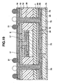
- FIG. 16 is a sectional view showing a semiconductor package according to the second example.
- a ground layer 51 made of, e.g., a copper foil is formed at a predetermined portion of the upper surface of a base plate 1.
- the lower surface of a silicon substrate 4 of a semiconductor constructing body 2 is bonded to the upper surface of the ground layer 51 via an adhesive layer 3.
- the inner surface of a circular hole 52 formed at a predetermined portion of the ground layer 51 is connected to an underlying metal layer 28a of a vertical conducting portion 28.
- the circular hole 52 is formed in the ground layer 51 simultaneously with formation of through holes 27.
- the underlying metal layer 28a is formed in the through hole 27, the underlying metal layer 28a is connected to the inner surface of the circular hole 52 in the ground layer 51.
- FIG. 17 is a sectional view showing a semiconductor package according to the third example of the present invention.
- the vertical conducting portion 28 is connected to the ground layer 51.
- a lower interconnection 24 including a lower underlying metal layer 23 may be connected to a ground layer 51 through an opening portion 53 formed in a first lower insulating film 22 and base plate 1.
- FIG. 18 is a sectional view showing a semiconductor package according to the fourth example.
- the upper underlying metal layer 16 including only one layer is formed on the first upper insulating film 15, as shown in FIG. 1 .
- two layers or three or more layers may be formed.
- a first upper insulating film 61 made of a build-up material is formed on the upper surfaces of a semiconductor constructing body 2 and insulating layer 14.
- First upper interconnections 63 including first upper underlying metal layers 62 are formed on the upper surface of the first upper insulating film 61 and connected to the upper surfaces of columnar electrodes 12 through opening portions 64 formed in the first upper insulating film 61.
- a second upper insulating film 65 made of a build-up material is formed on the upper surface of the first upper insulating film 61 including the first upper interconnections 63.
- Second upper interconnections 67 including second underlying metal layers 66 are formed on the upper surface of the second upper insulating film 65 and connected to the connection pad portions of the first upper interconnections 63 through opening portions 68 formed in the second upper insulating film 65.
- a third upper insulating film 69 made of solder resist is formed on the upper surface of the second upper insulating film 65 including the second upper interconnections 67. Opening portions 70 are formed in the third upper insulating film 69 at portions corresponding to the connection pad portions of the second upper interconnections 67. A solder ball 71 is formed in and above each opening portion 70 and connected to the connection pad portion of a corresponding one of the second upper interconnections 67.
- the first upper interconnections 63 including the first upper underlying metal layers 62 and lower interconnections 24 including lower underlying metal layers 23 are connected through vertical conducting portions 28.
- the second upper interconnections 67 including the second underlying metal layers 66 and the lower interconnections 24 including the lower underlying metal layers 23 may be connected through the vertical conducting portions 28.
- the solder balls 71 are formed only on a region corresponding to the insulating layer 14 having a rectangular frame shape around the semiconductor constructing body 2.
- most part of the upper surface of the second upper insulating film 65 in a region corresponding to the semiconductor constructing body 2 is an extra region which can be prevented from having the second upper interconnections 67 connected to the solder balls 71.
- the size of an electronic device may be reduced by forming, in this extra region, a thin-film passive element 72 such as a capacitor circuit element, inductor circuit element, or antenna circuit element formed from the second upper interconnection.
- a chip component 73 such as a capacitor or resistor may be mounted at a predetermined portion of the peripheral portion of the upper surface of a second lower insulating film 25 to further reduce the device size and wiring length.
- the two electrodes of the chip component 73 are connected to the lower interconnections 24 through solder portions 74 which fill opening portions 26 by screen printing.
- the thin-film passive element 72 such as a capacitor circuit element, inductor circuit element, or antenna circuit element formed from the lower interconnection may be formed on the upper surface of the first lower insulating film 22 in a region except the mounting region of the chip component 73. In this case, a relatively large area can be ensured as the formation region of the thin-film passive element 72. Hence, the passive element having a relatively large area can satisfactorily be formed.
- the chip component 73 is formed at the peripheral portion of the upper surface of the second lower insulating film 25 so that the second lower insulating film 25 has a flat region almost at the central portion of the upper surface.
- the flat region at the central portion can be used as a suction head suction region (mounting pickup region) which is sucked by a suction head to handle the semiconductor device.
- a plurality of chip components 73 may be mounted almost on the entire region of the upper surface including a portion near the central portion of the upper surface of the second lower insulating film 25. In this case, the device size and wiring length can further be reduced. However, it becomes difficult to ensure a flat suction head suction region.
- the fifth and sixth embodiments will be described below, in which a flat suction head suction region can be ensured even in the above case.
- FIG. 19 is a sectional view showing a semiconductor package according to the first embodiment of the present invention.
- a plurality of chip components 73 are mounted on the entire region including almost the central portion of the upper surface of a second lower insulating film 25. These chip components 73 are covered with a sealing film 75 made of epoxy resin or polyimide resin. The upper surface of the sealing film 75 is planarized by polishing. The flat upper surface is used as a suction head suction region.
- FIG. 20 is a sectional view showing a semiconductor package according to the second embodiment of the present invention.
- a plurality of chip components 73 are mounted on the entire region including almost the central portion of the upper surface of a second lower insulating film 25.
- the chip component 73 mounted almost at the central portion of the upper surface of the second lower insulating film 25 is covered with a sealing film 75 made of epoxy resin or polyimide resin.
- a flat plate 76 formed from a metal plate is bonded to the upper surface of the sealing film 75. The upper surface of the flat plate 76 is used as a suction head suction region.
- a semiconductor IC chip made of an integrated circuit such as an LSI or a structure similar to the semiconductor constructing body 2 shown in FIG. 1 may be mounted.
- FIG. 21 is a sectional view showing a semiconductor package according to the fifth example .
- the lower interconnections 24 each including only one layer are formed under the first lower insulating film 22, as shown in FIG. 1 .
- the present invention is not limited to this.
- two layers or three or more layers may be formed.
- a first lower insulating film 101 made of a build-up material is formed on the lower surface of a base plate 1.
- First lower interconnections 103 including lower underlying metal layers 102 are formed on the lower surface of the first lower insulating film 101 and connected to vertical conducting portions 28.
- a second lower insulating film 104 made of a build-up material is formed on the lower surface of the first lower insulating film 101 including the first lower interconnections 103.
- Second lower interconnections 106 including second lower underlying metal layers 105 are formed on the lower surface of the second lower insulating film 104 and connected to the connection pad portions of the first lower interconnections 103 through opening portions 107 formed in the second lower insulating film 104.
- a third lower insulating film 108 made of solder resist is formed on the lower surface of the second lower insulating film 104 including the second lower interconnections 106. Opening portions 109 are formed in the third lower insulating film 108 at portions corresponding to the connection pad portions of the second lower interconnections 106.
- upper interconnections 17 including upper underlying metal layers 16 and the first lower interconnections 103 including the lower underlying metal layers 102 are connected through the vertical conducting portions 28.
- the upper interconnections 17 including the upper underlying metal layers 16 and the second lower interconnections 106 including the second lower underlying metal layers 105 may be connected through the vertical conducting portions.
- each upper interconnection includes two or more layers
- each lower interconnection includes two or more layers
- one of the layers of the upper interconnection and one of the layers of the lower interconnection may be connected through a vertical conducting portion, including the cases shown in FIGS. 18 and 21 .
- FIG. 22 is a sectional view showing a semiconductor package according to the sixth example.
- the resultant structure is cut between the semiconductor constructing bodies 2 adjacent to each other.
- the resultant structure may be cut for every two semiconductor constructing bodies 2 to obtain a multichip module type semiconductor device.
- the resultant structure may be cut for every two or more semiconductor constructing bodies 2.
- the semiconductor constructing bodies 2 of one set can be either of the same type or of different types.
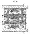
- FIG. 23 is a sectional view showing a semiconductor package according to the seventh example of the present invention.
- second and third semiconductor packages 82 and 83 are mounted under a first semiconductor package 81 having, e.g., the same structure as shown in FIG. 1 .
- the second semiconductor block 82 has no solder balls 21, unlike, e.g., the structure shown in FIG. 1 .
- the third semiconductor block 83 has no through holes 27, vertical conducting portions 28, conductive materials 29, first lower insulating film 22, second lower insulating film 25, lower underlying metal layers 23, lower interconnections 24, and solder balls 21, unlike, e.g., the structure shown in FIG. 1 .
- the first semiconductor block 81 and the second semiconductor block 82 are bonded via an adhesive layer 84 inserted between them.
- the connection pad portions of the lower interconnections 24 of the first semiconductor block 81 are connected to the connection pad portions of upper interconnections 17 of the second semiconductor block 82 through conductive materials 86 formed in through holes 85 formed in the adhesive layer 84.
- the second semiconductor block 82 and the third semiconductor block 83 are bonded via an adhesive layer 87 inserted between them.
- the connection pad portions of the lower interconnections 24 of the second semiconductor block 82 are connected to the connection pad portions of the upper interconnections 17 of the third semiconductor block 83 through conductive materials 89 formed in through holes 88 formed in the adhesive layer 87.
- FIGS. 24 and 25 are sectional views showing an example of a manufacturing method applied to the semiconductor package according to the seventh example.
- the adhesive layer 84 which has a thin sheet shape and is made of a thermosetting resin such as liquid crystal polymer, thermoplastic polyimide, PEEK (polyetheretherketone), or PPS (polyphenylene-sulfide) is bonded to the upper surface of a second upper insulating film 19 of the second semiconductor block 82.
- a protective film 90 is bonded to the upper surface of the adhesive layer 84.
- the through holes 85 are formed in the protective film 90 and adhesive layer 84 at portions corresponding to opening portions 20 of a second upper insulating film 19, i.e., the connection pad portions of the upper interconnections 17 by, e.g., laser machining for irradiating the structure with a laser beam.
- the through holes 85 and opening portions 20 are filled with the conductive material 86 such as copper paste, silver paste, or a conductive resin, which can be sintered at a low temperature, by screen printing.
- the conductive material 86 such as copper paste, silver paste, or a conductive resin, which can be sintered at a low temperature, by screen printing.
- each conductive material 86 projects from the adhesive layer 84 while having a height equal to the thickness of the protective film 90.
- the third semiconductor block 83 is prepared by filling, with the conductive materials 89, the through holes 88 and the like formed in the adhesive layer 87 bonded to the upper surface of the second upper insulating film 19.
- the second semiconductor block 82 is placed on the adhesive layer 87 on the third semiconductor block 83.
- the first semiconductor block 81 is placed on the adhesive layer 84 on the second semiconductor block 82. In this case, no solder balls 21 are formed on the first semiconductor block 81.
- the upper portions of the conductive materials 86 and 89 are inserted in opening portions 26 of the second lower insulating films 25 of the semiconductor blocks 81 and 82.
- the first to third semiconductor blocks 81 to 83 and the adhesive layers 84 and 87 are heated and pressed by using a pair of heating/pressing plates 91 and 92. Accordingly, the conductive materials 86 and 89 are sintered.
- the connection pad portions of the lower interconnections 24 of the first semiconductor block 81 are connected to the connection pad portions of the upper interconnections 17 of the second semiconductor block 82 through the conductive materials 86.
- the connection pad portions of the lower interconnections 24 of the second semiconductor block 82 are connected to the connection pad portions of the upper interconnections 17 of the third semiconductor block 83 through the conductive materials 89.
- the first semiconductor block 81 and second semiconductor block 82 are bonded via the adhesive layer 84 while the second semiconductor block 82 and third semiconductor block 83 are bonded via the adhesive layer 87.
- the solder balls 21 are formed on the first semiconductor block 81. In this way, the semiconductor device shown in FIG. 22 is obtained.
- the manufacturing step can be simplified.
- the solder balls 21 on the third semiconductor block 83 may be omitted, unlike, e.g., the structure shown in FIG. 1 .
- the semiconductor constructing body 2 has, as external connection electrodes, the columnar electrodes 12 formed on the connection pad portions of the interconnections 11.
- the semiconductor constructing body 2 may have no columnar electrodes 12 but the interconnections 11 having connection pad portions serving as external connection electrodes.
- the semiconductor constructing body 2 may have the connection pads 5 serving as external connection electrodes.
- columnar electrodes may be formed on the connection pads 5 as external connection electrodes.
- the columnar electrodes may be used as external connection electrode.
- solder balls 21 are connected to the connection pad portions of the upper interconnections 17 exposed from the opening portions 20 formed in the second upper insulating film 19.
- the solder balls 21 may be connected to the lower interconnections 24 exposed from the opening portions 26 formed in the second lower insulating film 25.
- the chip component 73 or semiconductor chip is mounted on the lower surface of the second lower insulating film 25 and connected to the lower interconnections 24.
- the chip component 73 or semiconductor chip may be mounted on the upper surface of the second upper insulating film 19 and connected to the connection pad portions of the upper interconnections 17.
Abstract
Claims (50)
- Boîtier de semi-conducteur comprenant :une plaque de base (1) comportant des première et deuxième surfaces planes ;au moins un composant semi-conducteur (2) sur ladite première surface de la plaque de base (1), le composant comportant un substrat semi-conducteur (4) avec une pluralité d'électrodes de connexion externes (12) formées sur celui-ci ;une couche isolante (14, 15) qui est formée sur la première surface de la plaque de base (1) autour du composant semi-conducteur (2) ;une pluralité d'interconnexions supérieures (16, 17), chacune d'elles étant formée sur la couche isolante (15) et comprenant au moins une couche d'interconnexion, au moins certaines des interconnexions supérieures (16, 17) étant connectées aux électrodes de connexion externes (12) du composant semi-conducteur (2) ; etune pluralité d'interconnexions inférieures (23, 24), chacune d'elles étant formée sur la deuxième surface de la plaque de base (1) et comprenant au moins une couche d'interconnexion, au moins certaines des interconnexions inférieures (23, 24) étant connectées électriquement aux interconnexions supérieures (16, 17) ;un film isolant supérieur (19) qui recouvre une surface supérieure de la couche isolante (15) et les interconnexions supérieures (16, 17) à l'exception des parties de borne de connexion (20) des interconnexions supérieures (16, 17) ;au moins une partie de borne de connexion formée sur l'interconnexion inférieure (23, 24) ; etun film isolant inférieur (22, 25) qui recouvre la deuxième surface de la plaque de base et les parties à l'exception des parties de borne de connexion des interconnexions inférieures ;caractérisé en ce queau moins un composant électronique est monté sur le film isolant inférieur (25) et est connecté à la partie de borne de connexion de l'interconnexion inférieure (23, 24) ;dans lequel ledit au moins un composant électronique comprend une pluralité de composants électroniques qui sont montés dans une région comprenant une partie centrale de la surface supérieure du film isolant inférieur (25), qui sont recouverts d'un film d'étanchéité (75) dont la surface supérieure est conçue pour être utilisée en tant que région de préhension par une tête d'aspiration ; etle composant semi-conducteur (2) comprend en outre une pluralité de pastilles de connexion (5) prévues sur le substrat semi-conducteur (4), les électrodes de connexion externes sont prévues en tant que pluralité d'électrodes en colonne (12) connectées électriquement aux pastilles de connexion (5), et un film d'étanchéité (13) est formé autour des électrodes en colonne (12).
- Boîtier de semi-conducteur comprenant :une plaque de base (1) comportant des première et deuxième surfaces planes ;au moins un composant semi-conducteur (2) sur ladite première surface de la plaque de base (1), et le composant comportant un substrat semi-conducteur (4) avec une pluralité d'électrodes de connexion externes (12) formées sur celui-ci ;une couche isolante (14, 15) qui est formée sur la première surface de la plaque de base (1) autour du composant semi-conducteur (2) ;une pluralité d'interconnexions supérieures (16, 17), chacune d'elles étant formée sur la couche isolante (15) et comprenant au moins une couche d'interconnexion, au moins certaines des interconnexions supérieures (16, 17) étant connectées aux électrodes de connexion externes (12) du composant semi-conducteur (2) ; etune pluralité d'interconnexions inférieures (23, 24), chacune d'elles étant formée sur ladite deuxième surface de la plaque de base (1) et comprenant au moins une couche d'interconnexion, au moins certaines des interconnexions inférieures (23, 24) étant connectées électriquement aux interconnexions supérieures (16, 17) ;un film isolant supérieur (19) qui recouvre une surface supérieure de la couche isolante (15) et les interconnexions supérieures (16, 17) à l'exception des parties de borne de connexion (20) des interconnexions supérieures (16, 17) ;au moins une partie de borne de connexion formée sur l'interconnexion inférieure (23, 24) ; etun film isolant inférieur (22, 25) qui recouvre ladite deuxième surface de la plaque de base et les parties à l'exception des parties de borne de connexion des interconnexions inférieures ;caractérisé en ce queau moins un composant électronique est monté sur le film isolant inférieur (25) et est connecté à la partie de borne de connexion de l'interconnexion inférieure (23, 24) ;dans lequel ledit au moins un composant électronique comprend une pluralité de composants électroniques qui sont montés dans une région comprenant une partie centrale de la surface supérieure du film isolant inférieur (25), au moins le composant électronique monté au niveau de la partie centrale de la surface supérieure du film isolant inférieur (25) est recouvert d'un film d'étanchéité (75), une plaque plate est placée sur une surface supérieure du film isolant, et une surface supérieure de la plaque plate est conçue pour être utilisée en tant que région de préhension par une tête d'aspiration ; etle composant semi-conducteur (2) comprend en outre une pluralité de pastilles de connexion (5) prévues sur le substrat semi-conducteur (4), les électrodes de connexion externes (12) sont prévues en tant que pluralité d'électrodes en colonne (12) connectées électriquement aux pastilles de connexion (5), et un film d'étanchéité (13) est formé autour des électrodes en colonne (12).
- Boîtier selon la revendication 1 ou 2, comprenant en outre au moins une électrode saillante (21) qui est formée sur la partie de borne de connexion (20) de l'interconnexion supérieure (16, 17).
- Boîtier selon la revendication 3, dans lequel l'électrode saillante (21) comprend une bille de soudure.
- Boîtier selon l'une quelconque des revendications 1 à 4, qui comprend en outre un autre film isolant (15) qui recouvre la surface supérieure entière de la couche isolante (14) et une surface supérieure du composant semi-conducteur (2) à l'exception d'une partie centrale d'une surface supérieure de chaque électrode de connexion externe (12), et dans lequel le film isolant supérieur et les interconnexions supérieures (16, 17) sont formés sur l'autre film isolant (15).
- Boîtier selon la revendication 5, dans lequel la couche isolante (15) a la forme d'une feuille.
- Boîtier selon la revendication 6, dans lequel la surface supérieure de la couche isolante (15) est plate.
- Boîtier selon l'une quelconque des revendications 1 à 7, dans lequel au moins un composant électronique est monté sur le film isolant supérieur et est connecté à la partie de borne de connexion (20) de l'interconnexion supérieure (16, 17).
- Boîtier selon l'une quelconque des revendications 1 à 8, comprenant en outre une partie conductrice verticale (28) qui connecte l'une des couches d'interconnexion de l'interconnexion supérieure (16, 17) à l'une des couches d'interconnexion de l'interconnexion inférieure (23, 24).
- Boîtier selon la revendication 9, dans lequel un trou traversant (27) est formé au moins dans la couche isolante (15) et la plaque de base (1), et la partie conductrice verticale (28) comprend au moins un matériau conducteur avec lequel le trou traversant (27) est rempli.
- Boîtier selon la revendication 10, dans lequel un trou traversant (27) est formé au moins dans la couche isolante (15) et la plaque de base (1), et la partie conductrice verticale (28) comprend au moins une couche d'interconnexion formée dans le trou traversant (27).
- Boîtier selon la revendication 10, dans lequel la partie conductrice verticale (28) comprend en outre un matériau conducteur avec lequel le trou traversant (27) est rempli.
- Boîtier selon la revendication 9, comprenant en outre une couche de masse (3) qui est formée sur une surface supérieure de la plaque de base (1), et sur laquelle le composant semi-conducteur (2) est formé.
- Boîtier selon la revendication 13, dans lequel la couche de masse (2) est connectée à la partie conductrice verticale (28).
- Boîtier selon l'une quelconque des revendications 1 à 14, dans lequel ledit au moins un composant semi-conducteur (2) comprend une pluralité de composants semi-conducteurs (2) formés sur la plaque de base (1).
- Boîtier selon la revendication 15, dans lequel ladite pluralité de composants semi-conducteurs (2) sont formés sur la plaque de base (1) tout en étant séparés les uns des autres.
- Boîtier selon la revendication 15, dans lequel au moins certaines des électrodes de connexion externes (12) de ladite pluralité de composants semi-conducteurs (2) sont connectées électriquement les unes aux autres par l'intermédiaire des interconnexions supérieures (16, 17).
- Boîtier selon l'une quelconque des revendications 1 à 17, dans lequel le composant semi-conducteur (2) comprend une interconnexion (10, 11) qui connecte la pastille de connexion (5) à l'électrode en colonne (12).
- Boîtier selon la revendication 1 ou 2, dans lequel le composant semi-conducteur (2) comprend une pluralité de pastilles de connexion (5), et les électrodes de connexion externes (12) comprennent les pastilles de connexion.
- Boîtier selon l'une quelconque des revendications 1 à 19, dans lequel au moins une électrode saillante est formée sur la partie de borne de connexion de l'interconnexion inférieure (23, 24).
- Boîtier selon la revendication 20, dans lequel l'électrode saillante comprend une bille de soudure.
- Boîtier selon l'une quelconque des revendications 1 à 21, qui comprend en outre un film isolant supplémentaire (22) qui recouvre la surface entière de ladite deuxième surface de la plaque de base, et dans lequel le film isolant inférieur (22, 25) et les interconnexions inférieures (23, 24) sont formés sur le film isolant supplémentaires (22).
- Boîtier selon la revendication 22, dans lequel le film isolant supplémentaire (22) a la forme d'une feuille.
- Boîtier selon l'une quelconque des revendications 1 à 23, dans lequel un élément de circuit à films minces est formé par au moins certaines des interconnexions inférieures (23, 24) ou certaines des interconnexions supérieures (16, 17).
- Boîtier selon la revendication 24, dans lequel l'élément de circuit à films minces comprend l'un d'un élément de circuit de condensateur, d'un élément de circuit d'inductance et d'un élément de circuit d'antenne.
- Boîtier selon l'une quelconque des revendications 1 à 25, comprenant en outre une couche de masse (3) qui est formée sur une surface supérieure de la plaque de base (1), et sur laquelle le composant semi-conducteur (2) est formé.
- Boîtier selon la revendication 26, dans lequel la couche de masse (3) est connectée à l'interconnexion inférieure (23, 24).
- Procédé de fabrication d'un boîtier de semi-conducteur consistant à :agencer, sur une première surface d'une plaque de base (1), comportant des première et deuxième surfaces planes, une pluralité de composants semi-conducteurs (2), chaque composant semi-conducteur (2) comprenant un substrat semi-conducteur (4) et une pluralité d'électrodes de connexion externes (12) formées sur celui-ci ;former une couche isolante (14, 15) sur la première surface de la plaque de base autour des composants semi-conducteurs (2) ;former, sur un côté supérieur de la couche isolante (15), des interconnexions supérieures (16, 17), chacune d'elles comprenant au moins une couche d'interconnexion et comportant au moins une partie de borne de connexion, au moins certaines des interconnexions supérieures (16, 17) étant connectées aux électrodes de connexion externes (12) des composants semi-conducteurs (2) ;former, sur la deuxième surface de la plaque de base (1), des interconnexions inférieures (23, 24), chacune d'elles comprenant au moins une couche d'interconnexion et au moins une partie de borne de connexion ;former un trou traversant (27) dans la couche isolante (14) et la plaque de base (1) ;former, dans le trou traversant (27), une partie conductrice verticale (28) qui connecte l'une des couches de l'interconnexion supérieure (16, 17) à l'une des couches de l'interconnexion inférieure (23, 24) ;former un film isolant inférieur (22, 25) qui recouvre la deuxième surface de la plaque de base et des parties à l'exception des parties de borne de connexion des interconnexions inférieures ;former au moins une partie de borne de connexion sur l'interconnexion inférieure (23, 24) ; etformer un film isolant supérieur (19) sur une surface supérieure de la couche isolante (15) et sur les interconnexions supérieures (16, 17) à l'exception des parties de borne de connexion (20) des interconnexions supérieures (16, 17) ;caractérisé en ce qu'il consiste en outre àmonter au moins un composant électronique sur le film isolant inférieur (25) et connecter le composant électronique à la partie de borne de connexion de l'interconnexion inférieure (22, 25) ; dans lequel ledit au moins un composant électronique comprend une pluralité de composants électroniques qui sont montés dans une région comprenant une partie centrale de la surface supérieure du film isolant inférieur (25) ;recouvrir ladite pluralité de composants électroniques avec un film d'étanchéité (75) ;utiliser le film d'étanchéité en tant que région de préhension pour une tête d'aspiration ; dans lequelchaque composant semi-conducteur (2) comprend en outre une pluralité de pastilles de connexion (5), les électrodes de connexion externes sont prévues en tant que pluralité d'électrodes en colonne (12) qui sont connectées électriquement aux pastilles de connexion (5), et un film d'étanchéité (13) est formé autour des électrodes en colonne (12) formées sur un côté d'un substrat semi-conducteur (4) tout en séparant les composants semi-conducteurs (2) les uns des autres.
- Procédé de fabrication d'un boîtier de semi-conducteur consistant à :agencer, sur une première surface d'une plaque de base (1), comportant des première et deuxième surfaces planes, une pluralité de composants semi-conducteurs (2), chaque composant semi-conducteur (2) comprenant un substrat semi-conducteur (4) et une pluralité d'électrodes de connexion externes (12) formées sur celui-ci ;former une couche isolante (14, 15) sur la première surface de la plaque de base autour des composants semi-conducteurs (2) ;former, sur un côté supérieur de la couche isolante (15), des interconnexions supérieures (16, 17), chacune d'elles comprenant au moins une couche d'interconnexion et comportant au moins une partie de borne de connexion, au moins certaines des interconnexions supérieures (16, 17) étant connectées aux électrodes de connexion externes (12) des composants semi-conducteurs (2) ;former, sur la deuxième surface de la plaque de base (1), des interconnexions inférieures (23, 24), chacune d'elles comprenant au moins une couche d'interconnexion et au moins une partie de borne de connexion ;former un trou traversant (27) dans la couche isolante (14) et la plaque de base (1) ;former, dans le trou traversant (27), une partie conductrice verticale (28) qui connecte l'une des couches de l'interconnexion supérieure (16, 17) à l'une des couches de l'interconnexion inférieure (23, 24) ;former un film isolant inférieur (22, 25) qui recouvre la deuxième surface de la plaque de base et des parties à
l'exception des parties de borne de connexion des interconnexions inférieures ;former au moins une partie de borne de connexion sur l'interconnexion inférieure (23, 24) ; etformer un film isolant supérieur (19) sur une surface supérieure de la couche isolante (15) et sur les interconnexions supérieures (16, 17) à l'exception des parties de borne de connexion (20) des interconnexions supérieures (16, 17) ;caractérisé en ce qu'il consiste en outre àmonter au moins un composant électronique sur le film isolant inférieur (25) et connecter le composant électronique à la partie de borne de connexion de l'interconnexion inférieure (22, 25) ; dans lequel ledit au moins un composant électronique comprend une pluralité de composants électroniques qui sont montés dans une région comprenant une partie centrale de la surface supérieure du film isolant inférieur (25) ;recouvrir le composant électronique monté dans la partie centrale de la surface supérieure du film isolant inférieur (25) avec un film d'étanchéité (75) ;placer une plaque plate sur une surface supérieure du film d'étanchéité (75) ; etutiliser la surface supérieure de la plaque plate en tant que région de préhension pour une tête d'aspiration ;dans lequelchaque composant semi-conducteur (2) comprend en outre une pluralité de pastilles de connexion (5), les électrodes de connexion externes sont prévues en tant que pluralité d'électrodes en colonne (12) qui sont connectées électriquement aux pastilles de connexion (5), et un film d'étanchéité (13) est formé autour des électrodes en colonne (12) formées sur un côté d'un substrat semi-conducteur (4) tout en séparant les composants semi-conducteurs (2) les uns des autres. - Procédé selon la revendication 28 ou 29, consistant en outre à découper la couche isolante (15) et la plaque de base (1) entre les composants semi-conducteurs (2) pour séparer les composants semi-conducteurs (2) en boîtiers de semi-conducteur comprenant chacun au moins un composant semi-conducteur (2).
- Procédé selon la revendication 30, dans lequel la coupe est effectuée de manière à faire en sorte que le boîtier de semi-conducteur comprenne une pluralité de composants semi-conducteurs (2).
- Procédé selon la revendication 28 ou 29, dans lequel la formation d'une couche d'interconnexion la plus basse de l'interconnexion supérieure (16) et la formation d'une couche d'interconnexion la plus haute de l'interconnexion inférieure (23) sont exécutées simultanément.
- Procédé selon la revendication 32, dans lequel la formation de la partie conductrice verticale (28a) est exécutée simultanément avec la formation de la couche d'interconnexion la plus basse de l'interconnexion supérieure (16) et la formation de la couche d'interconnexion la plus haute de l'interconnexion inférieure (23).
- Procédé selon l'une quelconque des revendications 28 à 33, dans lequel la formation de la partie conductrice verticale (28) comprend le remplissage du trou traversant (27) avec un matériau conducteur.
- Procédé selon la revendication 34, dans lequel le matériau conducteur comprend l'une d'une pâte de cuivre, d'une pâte d'argent et d'une résine conductrice.
- Procédé selon l'une quelconque des revendications 28 à 35, dans lequel le composant semi-conducteur (2) comprend une interconnexion qui connecte la pastille de connexion (5) à l'électrode en colonne (12).
- Procédé selon l'une quelconque des revendications 28 à 36, dans lequel le composant semi-conducteur (2) comprend une pluralité de pastilles de connexion, et les électrodes de connexion externes (12) comprennent les pastilles de connexion.
- Procédé selon l'une quelconque des revendications 28 à 37, dans lequel le film isolant supérieur (19) a la forme d'une feuille.
- Procédé selon la revendication 38, dans lequel la formation du film isolant supérieur (19) consiste à aplanir une surface supérieure du film isolant.
- Procédé selon la revendication 28, consistant en outre à monter au moins un composant électronique sur le film isolant supérieur et connecter le composant électronique à la partie de borne de connexion (20) de l'interconnexion supérieure (16, 17).
- Procédé selon la revendication 28, consistant en outre à former une électrode saillante sur la partie de borne de connexion de l'interconnexion supérieure (16, 17).
- Procédé selon la revendication 41, dans lequel l'électrode saillante comprend une bille de soudure.
- Procédé selon l'une quelconque des revendications 28 à 42, qui consiste en outre à former un film isolant (26) sur une surface entière de ladite deuxième surface de la plaque de base, et dans lequel la formation du film isolant inférieur (22, 25) et des interconnexions inférieures (23, 24) comprend la formation du film isolant inférieur et des interconnexions inférieures sur le film isolant.
- Procédé selon la revendication 43, dans lequel le film isolant (26) a la forme d'une feuille.
- Procédé selon l'une quelconque des revendications 28 à 44, consistant en outre à former une électrode saillante sur la partie de borne de connexion de l'interconnexion inférieure (23, 24).
- Procédé selon la revendication 45, dans lequel l'électrode saillante comprend une bille de soudure.
- Procédé selon la revendication 28 ou 29, consistant en outre à former un élément de circuit à films minces par au moins certaines des interconnexions inférieures (23, 24) ou certaines des interconnexions supérieures (16, 17).
- Procédé selon la revendication 47, dans lequel l'élément de circuit à films minces comprend l'un d'un élément de circuit de condensateur, d'un élément de circuit d'inductance et d'un élément de circuit d'antenne.
- Procédé selon la revendication 28 ou 29, consistant en outre à former une couche de masse (3) sur une surface supérieure de la plaque de base (1).
- Procédé selon la revendication 49, consistant en outre à connecter la couche de masse (3) à l'une de la partie conductrice verticale (28) et de l'interconnexion inférieure (23, 24).
Applications Claiming Priority (2)
| Application Number | Priority Date | Filing Date | Title |
|---|---|---|---|
| JP2003158489 | 2003-06-03 | ||
| PCT/JP2004/007862 WO2004109771A2 (fr) | 2003-06-03 | 2004-05-31 | Boitier a semi-conducteur dote d'un corps de construction a semi-conducteur et son procede de production |
Publications (2)
| Publication Number | Publication Date |
|---|---|
| EP1636842A2 EP1636842A2 (fr) | 2006-03-22 |
| EP1636842B1 true EP1636842B1 (fr) | 2011-08-17 |
Family
ID=33487434
Family Applications (1)
| Application Number | Title | Priority Date | Filing Date |
|---|---|---|---|
| EP04735511A Expired - Fee Related EP1636842B1 (fr) | 2003-06-03 | 2004-05-31 | Dispositif semi-conducteur empilable et procede de sa fabrication |
Country Status (7)
| Country | Link |
|---|---|
| US (2) | US7709942B2 (fr) |
| EP (1) | EP1636842B1 (fr) |
| KR (1) | KR100778597B1 (fr) |
| CN (1) | CN100468719C (fr) |
| HK (1) | HK1086386A1 (fr) |
| TW (1) | TWI247373B (fr) |
| WO (1) | WO2004109771A2 (fr) |
Families Citing this family (68)
| Publication number | Priority date | Publication date | Assignee | Title |
|---|---|---|---|---|
| US7208825B2 (en) * | 2003-01-22 | 2007-04-24 | Siliconware Precision Industries Co., Ltd. | Stacked semiconductor packages |
| TWI278048B (en) | 2003-11-10 | 2007-04-01 | Casio Computer Co Ltd | Semiconductor device and its manufacturing method |
| JP3945483B2 (ja) | 2004-01-27 | 2007-07-18 | カシオ計算機株式会社 | 半導体装置の製造方法 |
| JP4093186B2 (ja) * | 2004-01-27 | 2008-06-04 | カシオ計算機株式会社 | 半導体装置の製造方法 |
| JP3925809B2 (ja) * | 2004-03-31 | 2007-06-06 | カシオ計算機株式会社 | 半導体装置およびその製造方法 |
| US7215018B2 (en) | 2004-04-13 | 2007-05-08 | Vertical Circuits, Inc. | Stacked die BGA or LGA component assembly |
| JP4398305B2 (ja) * | 2004-06-02 | 2010-01-13 | カシオ計算機株式会社 | 半導体装置およびその製造方法 |
| JP2006173232A (ja) * | 2004-12-14 | 2006-06-29 | Casio Comput Co Ltd | 半導体装置およびその製造方法 |
| KR100621438B1 (ko) * | 2005-08-31 | 2006-09-08 | 삼성전자주식회사 | 감광성 폴리머를 이용한 적층 칩 패키지 및 그의 제조 방법 |
| JP4395775B2 (ja) * | 2005-10-05 | 2010-01-13 | ソニー株式会社 | 半導体装置及びその製造方法 |
| GB0613360D0 (en) | 2006-07-05 | 2006-08-16 | Iti Scotland Ltd | Bar code authentication |
| US7829438B2 (en) | 2006-10-10 | 2010-11-09 | Tessera, Inc. | Edge connect wafer level stacking |
| US8513789B2 (en) | 2006-10-10 | 2013-08-20 | Tessera, Inc. | Edge connect wafer level stacking with leads extending along edges |
| US7901989B2 (en) | 2006-10-10 | 2011-03-08 | Tessera, Inc. | Reconstituted wafer level stacking |
| KR100852603B1 (ko) * | 2006-12-27 | 2008-08-14 | 동부일렉트로닉스 주식회사 | 반도체소자 및 그 제조방법 |
| US7952195B2 (en) | 2006-12-28 | 2011-05-31 | Tessera, Inc. | Stacked packages with bridging traces |
| JP2008226945A (ja) * | 2007-03-09 | 2008-09-25 | Casio Comput Co Ltd | 半導体装置およびその製造方法 |
| US8723332B2 (en) * | 2007-06-11 | 2014-05-13 | Invensas Corporation | Electrically interconnected stacked die assemblies |
| US8237259B2 (en) * | 2007-06-13 | 2012-08-07 | Infineon Technologies Ag | Embedded chip package |
| US8461672B2 (en) | 2007-07-27 | 2013-06-11 | Tessera, Inc. | Reconstituted wafer stack packaging with after-applied pad extensions |
| WO2009020572A2 (fr) | 2007-08-03 | 2009-02-12 | Tessera Technologies Hungary Kft. | Ensembles empilés utilisant des tranches reconstituées |
| WO2009020240A2 (fr) * | 2007-08-08 | 2009-02-12 | Casio Computer Co., Ltd. | Dispositif à semi-conducteur et procédé servant à fabriquer celui-ci |
| JP2009043857A (ja) * | 2007-08-08 | 2009-02-26 | Casio Comput Co Ltd | 半導体装置およびその製造方法 |
| US8043895B2 (en) | 2007-08-09 | 2011-10-25 | Tessera, Inc. | Method of fabricating stacked assembly including plurality of stacked microelectronic elements |
| KR100885924B1 (ko) | 2007-08-10 | 2009-02-26 | 삼성전자주식회사 | 묻혀진 도전성 포스트를 포함하는 반도체 패키지 및 그제조방법 |
| JP4752825B2 (ja) * | 2007-08-24 | 2011-08-17 | カシオ計算機株式会社 | 半導体装置の製造方法 |
| US8704379B2 (en) | 2007-09-10 | 2014-04-22 | Invensas Corporation | Semiconductor die mount by conformal die coating |
| JP4636090B2 (ja) | 2008-01-31 | 2011-02-23 | カシオ計算機株式会社 | 半導体装置およびその製造方法 |
| JP4840373B2 (ja) * | 2008-01-31 | 2011-12-21 | カシオ計算機株式会社 | 半導体装置およびその製造方法 |
| CA2715344C (fr) * | 2008-02-14 | 2014-08-19 | Mitsubishi Heavy Industries, Ltd. | Module d'element semi-conducteur et son procede de fabrication |
| TWI422058B (zh) * | 2008-03-04 | 2014-01-01 | Everlight Electronics Co Ltd | 發光二極體封裝結構與其製造方法 |
| KR100927773B1 (ko) | 2008-03-11 | 2009-11-20 | 앰코 테크놀로지 코리아 주식회사 | 반도체 패키지 및 그 제조 방법 |
| WO2009114670A2 (fr) | 2008-03-12 | 2009-09-17 | Vertical Circuits, Inc. | Ensemble de dés interconnectés électriquement montés sur un support |
| US7863159B2 (en) | 2008-06-19 | 2011-01-04 | Vertical Circuits, Inc. | Semiconductor die separation method |
| US9153517B2 (en) | 2008-05-20 | 2015-10-06 | Invensas Corporation | Electrical connector between die pad and z-interconnect for stacked die assemblies |
| US8680662B2 (en) | 2008-06-16 | 2014-03-25 | Tessera, Inc. | Wafer level edge stacking |
| US8466542B2 (en) | 2009-03-13 | 2013-06-18 | Tessera, Inc. | Stacked microelectronic assemblies having vias extending through bond pads |
| FR2946795B1 (fr) * | 2009-06-12 | 2011-07-22 | 3D Plus | Procede de positionnement des puces lors de la fabrication d'une plaque reconstituee |
| TWI570879B (zh) | 2009-06-26 | 2017-02-11 | 英維瑟斯公司 | 半導體總成及晶粒堆疊總成 |
| US9147583B2 (en) | 2009-10-27 | 2015-09-29 | Invensas Corporation | Selective die electrical insulation by additive process |
| TWI544604B (zh) | 2009-11-04 | 2016-08-01 | 英維瑟斯公司 | 具有降低應力電互連的堆疊晶粒總成 |
| US8987896B2 (en) * | 2009-12-16 | 2015-03-24 | Intel Corporation | High-density inter-package connections for ultra-thin package-on-package structures, and processes of forming same |
| JP5563814B2 (ja) * | 2009-12-18 | 2014-07-30 | 新光電気工業株式会社 | 半導体装置及びその製造方法 |
| US8343810B2 (en) * | 2010-08-16 | 2013-01-01 | Stats Chippac, Ltd. | Semiconductor device and method of forming Fo-WLCSP having conductive layers and conductive vias separated by polymer layers |
| DE102010041129A1 (de) * | 2010-09-21 | 2012-03-22 | Robert Bosch Gmbh | Multifunktionssensor als PoP-mWLP |
| US9601434B2 (en) | 2010-12-10 | 2017-03-21 | STATS ChipPAC Pte. Ltd. | Semiconductor device and method of forming openings through insulating layer over encapsulant for enhanced adhesion of interconnect structure |
| TWI458026B (zh) * | 2012-01-13 | 2014-10-21 | Dawning Leading Technology Inc | 內嵌封裝體之封裝模組及其製造方法 |
| US8901730B2 (en) | 2012-05-03 | 2014-12-02 | Taiwan Semiconductor Manufacturing Company, Ltd. | Methods and apparatus for package on package devices |
| US9343442B2 (en) | 2012-09-20 | 2016-05-17 | Taiwan Semiconductor Manufacturing Company, Ltd. | Passive devices in package-on-package structures and methods for forming the same |
| US9312231B2 (en) * | 2013-10-31 | 2016-04-12 | Freescale Semiconductor, Inc. | Method and apparatus for high temperature semiconductor device packages and structures using a low temperature process |
| US9698116B2 (en) | 2014-10-31 | 2017-07-04 | Nxp Usa, Inc. | Thick-silver layer interface for a semiconductor die and corresponding thermal layer |
| JP6695066B2 (ja) * | 2014-11-27 | 2020-05-20 | ツーハイ アクセス セミコンダクター カンパニー リミテッド | フレームがコンデンサと直列に少なくとも1個のビアを備えるようなチップ用のポリマーフレーム |
| TW201526315A (zh) * | 2015-02-17 | 2015-07-01 | Xiu-Zhang Huang | 覆晶式發光二極體及其製造方法 |
| US9825002B2 (en) | 2015-07-17 | 2017-11-21 | Invensas Corporation | Flipped die stack |
| US9871019B2 (en) | 2015-07-17 | 2018-01-16 | Invensas Corporation | Flipped die stack assemblies with leadframe interconnects |
| US9490195B1 (en) | 2015-07-17 | 2016-11-08 | Invensas Corporation | Wafer-level flipped die stacks with leadframes or metal foil interconnects |
| US9508691B1 (en) | 2015-12-16 | 2016-11-29 | Invensas Corporation | Flipped die stacks with multiple rows of leadframe interconnects |
| US10566310B2 (en) | 2016-04-11 | 2020-02-18 | Invensas Corporation | Microelectronic packages having stacked die and wire bond interconnects |
| US9595511B1 (en) | 2016-05-12 | 2017-03-14 | Invensas Corporation | Microelectronic packages and assemblies with improved flyby signaling operation |
| US9728524B1 (en) | 2016-06-30 | 2017-08-08 | Invensas Corporation | Enhanced density assembly having microelectronic packages mounted at substantial angle to board |
| US10211137B2 (en) | 2017-06-08 | 2019-02-19 | Advanced Semiconductor Engineering, Inc. | Semiconductor device package |
| US11049803B2 (en) * | 2017-11-17 | 2021-06-29 | Mitsubishi Electric Corporation | Semiconductor module |
| US11315891B2 (en) | 2018-03-23 | 2022-04-26 | Taiwan Semiconductor Manufacturing Company, Ltd. | Methods of forming semiconductor packages having a die with an encapsulant |
| DE102018123924A1 (de) * | 2018-09-27 | 2020-04-02 | Infineon Technologies Ag | Eine Halbleitervorrichtung mit einer Lotverbindung, die eine Verbindung Sn/Sb aufweist |
| US11056443B2 (en) | 2019-08-29 | 2021-07-06 | Micron Technology, Inc. | Apparatuses exhibiting enhanced stress resistance and planarity, and related methods |
| CN112701444B (zh) * | 2019-10-22 | 2022-06-28 | 华为技术有限公司 | 天线、天线封装方法及终端 |
| KR20220097718A (ko) * | 2020-12-31 | 2022-07-08 | 삼성전자주식회사 | 배선 기판 및 이를 포함하는 반도체 모듈 |
| JP7410898B2 (ja) * | 2021-03-11 | 2024-01-10 | アオイ電子株式会社 | 半導体装置の製造方法および半導体装置 |
Citations (2)
| Publication number | Priority date | Publication date | Assignee | Title |
|---|---|---|---|---|
| US5875100A (en) * | 1996-05-31 | 1999-02-23 | Nec Corporation | High-density mounting method and structure for electronic circuit board |
| JP2001274034A (ja) * | 2000-01-20 | 2001-10-05 | Shinko Electric Ind Co Ltd | 電子部品パッケージ |
Family Cites Families (45)
| Publication number | Priority date | Publication date | Assignee | Title |
|---|---|---|---|---|
| US5337027A (en) * | 1992-12-18 | 1994-08-09 | General Electric Company | Microwave HDI phase shifter |
| JPH09116273A (ja) * | 1995-08-11 | 1997-05-02 | Shinko Electric Ind Co Ltd | 多層回路基板及びその製造方法 |
| JPH10100026A (ja) * | 1996-09-30 | 1998-04-21 | Toshiba Corp | 電子部品の搬送装置とこの搬送装置を使用した電子部品装着機 |
| US6525414B2 (en) | 1997-09-16 | 2003-02-25 | Matsushita Electric Industrial Co., Ltd. | Semiconductor device including a wiring board and semiconductor elements mounted thereon |
| JPH11265975A (ja) | 1998-03-17 | 1999-09-28 | Mitsubishi Electric Corp | 多層化集積回路装置 |
| KR100290784B1 (ko) * | 1998-09-15 | 2001-07-12 | 박종섭 | 스택 패키지 및 그 제조방법 |
| DE60023202T2 (de) | 1999-02-15 | 2006-07-20 | Mitsubishi Gas Chemical Co., Inc. | Leiterplatte für Plastikhalbleitergehäuse |
| JP3792445B2 (ja) | 1999-03-30 | 2006-07-05 | 日本特殊陶業株式会社 | コンデンサ付属配線基板 |
| JP2001044362A (ja) | 1999-07-27 | 2001-02-16 | Mitsubishi Electric Corp | 半導体装置の実装構造および実装方法 |
| JP3619395B2 (ja) | 1999-07-30 | 2005-02-09 | 京セラ株式会社 | 半導体素子内蔵配線基板およびその製造方法 |
| JP2001094046A (ja) | 1999-09-22 | 2001-04-06 | Seiko Epson Corp | 半導体装置 |
| JP3409759B2 (ja) | 1999-12-09 | 2003-05-26 | カシオ計算機株式会社 | 半導体装置の製造方法 |
| JP3670917B2 (ja) * | 1999-12-16 | 2005-07-13 | 新光電気工業株式会社 | 半導体装置及びその製造方法 |
| US6538210B2 (en) * | 1999-12-20 | 2003-03-25 | Matsushita Electric Industrial Co., Ltd. | Circuit component built-in module, radio device having the same, and method for producing the same |
| JP3813402B2 (ja) * | 2000-01-31 | 2006-08-23 | 新光電気工業株式会社 | 半導体装置の製造方法 |
| JP4854845B2 (ja) | 2000-02-25 | 2012-01-18 | イビデン株式会社 | 多層プリント配線板 |
| JP3651346B2 (ja) | 2000-03-06 | 2005-05-25 | カシオ計算機株式会社 | 半導体装置およびその製造方法 |
| KR100344833B1 (ko) * | 2000-04-03 | 2002-07-20 | 주식회사 하이닉스반도체 | 반도체 패키지 및 그의 제조방법 |
| JP3951091B2 (ja) | 2000-08-04 | 2007-08-01 | セイコーエプソン株式会社 | 半導体装置の製造方法 |
| JP4183375B2 (ja) * | 2000-10-04 | 2008-11-19 | 沖電気工業株式会社 | 半導体装置及びその製造方法 |
| JP2002134658A (ja) | 2000-10-24 | 2002-05-10 | Shinko Electric Ind Co Ltd | 半導体装置及びその製造方法 |
| TW511405B (en) * | 2000-12-27 | 2002-11-21 | Matsushita Electric Ind Co Ltd | Device built-in module and manufacturing method thereof |
| TW511415B (en) * | 2001-01-19 | 2002-11-21 | Matsushita Electric Ind Co Ltd | Component built-in module and its manufacturing method |
| JP2002270712A (ja) | 2001-03-14 | 2002-09-20 | Sony Corp | 半導体素子内蔵多層配線基板と半導体素子内蔵装置、およびそれらの製造方法 |
| JP3767398B2 (ja) * | 2001-03-19 | 2006-04-19 | カシオ計算機株式会社 | 半導体装置およびその製造方法 |
| JP3999945B2 (ja) * | 2001-05-18 | 2007-10-31 | 株式会社東芝 | 半導体装置の製造方法 |
| US20020175402A1 (en) * | 2001-05-23 | 2002-11-28 | Mccormack Mark Thomas | Structure and method of embedding components in multi-layer substrates |
| JP2002368184A (ja) | 2001-06-08 | 2002-12-20 | Nec Kyushu Ltd | マルチチップ半導体装置 |
| US6713860B2 (en) * | 2002-02-01 | 2004-03-30 | Intel Corporation | Electronic assembly and system with vertically connected capacitors |
| JP2003197849A (ja) | 2001-10-18 | 2003-07-11 | Matsushita Electric Ind Co Ltd | 部品内蔵モジュールとその製造方法 |
| JP3861669B2 (ja) * | 2001-11-22 | 2006-12-20 | ソニー株式会社 | マルチチップ回路モジュールの製造方法 |
| JP3870778B2 (ja) | 2001-12-20 | 2007-01-24 | ソニー株式会社 | 素子内蔵基板の製造方法および素子内蔵基板 |
| US6680529B2 (en) | 2002-02-15 | 2004-01-20 | Advanced Semiconductor Engineering, Inc. | Semiconductor build-up package |
| JP2003273321A (ja) | 2002-03-13 | 2003-09-26 | Toshiba Corp | 半導体モジュール |
| JP2003318361A (ja) | 2002-04-19 | 2003-11-07 | Fujitsu Ltd | 半導体装置及びその製造方法 |
| US6770971B2 (en) * | 2002-06-14 | 2004-08-03 | Casio Computer Co., Ltd. | Semiconductor device and method of fabricating the same |
| JP3918681B2 (ja) | 2002-08-09 | 2007-05-23 | カシオ計算機株式会社 | 半導体装置 |
| KR100593049B1 (ko) * | 2002-08-09 | 2006-06-28 | 가시오게산키 가부시키가이샤 | 반도체 장치 및 그 제조방법 |
| US7035113B2 (en) | 2003-01-30 | 2006-04-25 | Endicott Interconnect Technologies, Inc. | Multi-chip electronic package having laminate carrier and method of making same |
| TWI278048B (en) * | 2003-11-10 | 2007-04-01 | Casio Computer Co Ltd | Semiconductor device and its manufacturing method |
| JP4432470B2 (ja) * | 2003-11-25 | 2010-03-17 | 株式会社デンソー | 半導体装置 |
| JP3795040B2 (ja) * | 2003-12-03 | 2006-07-12 | 沖電気工業株式会社 | 半導体装置の製造方法 |
| US7489032B2 (en) | 2003-12-25 | 2009-02-10 | Casio Computer Co., Ltd. | Semiconductor device including a hard sheet to reduce warping of a base plate and method of fabricating the same |
| JP3945483B2 (ja) * | 2004-01-27 | 2007-07-18 | カシオ計算機株式会社 | 半導体装置の製造方法 |
| JP3925809B2 (ja) * | 2004-03-31 | 2007-06-06 | カシオ計算機株式会社 | 半導体装置およびその製造方法 |
-
2004
- 2004-05-31 EP EP04735511A patent/EP1636842B1/fr not_active Expired - Fee Related
- 2004-05-31 KR KR1020057012181A patent/KR100778597B1/ko not_active IP Right Cessation
- 2004-05-31 CN CNB2004800017045A patent/CN100468719C/zh not_active Expired - Fee Related
- 2004-05-31 WO PCT/JP2004/007862 patent/WO2004109771A2/fr active Application Filing
- 2004-06-02 US US10/860,478 patent/US7709942B2/en not_active Expired - Fee Related
- 2004-06-02 TW TW093115726A patent/TWI247373B/zh not_active IP Right Cessation
-
2006
- 2006-05-30 HK HK06106292.6A patent/HK1086386A1/xx not_active IP Right Cessation
-
2008
- 2008-03-12 US US12/047,228 patent/US7615411B2/en not_active Expired - Fee Related
Patent Citations (2)
| Publication number | Priority date | Publication date | Assignee | Title |
|---|---|---|---|---|
| US5875100A (en) * | 1996-05-31 | 1999-02-23 | Nec Corporation | High-density mounting method and structure for electronic circuit board |
| JP2001274034A (ja) * | 2000-01-20 | 2001-10-05 | Shinko Electric Ind Co Ltd | 電子部品パッケージ |
Also Published As
| Publication number | Publication date |
|---|---|
| US7615411B2 (en) | 2009-11-10 |
| EP1636842A2 (fr) | 2006-03-22 |
| KR20050087872A (ko) | 2005-08-31 |
| WO2004109771A2 (fr) | 2004-12-16 |
| US20040245614A1 (en) | 2004-12-09 |
| WO2004109771A3 (fr) | 2005-03-24 |
| CN1723556A (zh) | 2006-01-18 |
| CN100468719C (zh) | 2009-03-11 |
| KR100778597B1 (ko) | 2007-11-22 |
| HK1086386A1 (en) | 2006-09-15 |
| US20080166836A1 (en) | 2008-07-10 |
| TW200509270A (en) | 2005-03-01 |
| US7709942B2 (en) | 2010-05-04 |
| TWI247373B (en) | 2006-01-11 |
Similar Documents
| Publication | Publication Date | Title |
|---|---|---|
| EP1636842B1 (fr) | Dispositif semi-conducteur empilable et procede de sa fabrication | |
| US7042081B2 (en) | Semiconductor device having heat dissipation layer | |
| US6803324B2 (en) | Semiconductor device and its manufacturing method | |
| US7608480B2 (en) | Method of fabricating a semiconductor device incorporating a semiconductor constructing body and an interconnecting layer which is connected to a ground layer via a vertical conducting portion | |
| US8835221B2 (en) | Integrated chip package structure using ceramic substrate and method of manufacturing the same | |
| US8471361B2 (en) | Integrated chip package structure using organic substrate and method of manufacturing the same | |
| KR100727540B1 (ko) | 반도체 장치 및 그 제조 방법 | |
| US8429814B2 (en) | Method of assembling a multi-component electronic package | |
| US7413975B2 (en) | Interconnect substrate, semiconductor device, methods of manufacturing the same, circuit board, and electronic equipment | |
| EP1359618A2 (fr) | Dispositif semi-conducteur | |
| US20050161799A1 (en) | Semiconductor device having conducting portion of upper and lower conductive layers, and method of fabricating the same | |
| JP4157829B2 (ja) | 半導体装置およびその製造方法 | |
| JP4438389B2 (ja) | 半導体装置の製造方法 | |
| JP4341484B2 (ja) | 半導体装置およびその製造方法 |
Legal Events
| Date | Code | Title | Description |
|---|---|---|---|
| PUAI | Public reference made under article 153(3) epc to a published international application that has entered the european phase |
Free format text: ORIGINAL CODE: 0009012 |
|
| 17P | Request for examination filed |
Effective date: 20050506 |
|
| AK | Designated contracting states |
Kind code of ref document: A2 Designated state(s): DE FI FR GB NL |
|
| DAX | Request for extension of the european patent (deleted) | ||
| RBV | Designated contracting states (corrected) |
Designated state(s): DE FI FR GB NL |
|
| RAP1 | Party data changed (applicant data changed or rights of an application transferred) |
Owner name: CMK CORPORATION Owner name: CASIO COMPUTER CO., LTD. |
|
| 17Q | First examination report despatched |
Effective date: 20080128 |
|
| GRAP | Despatch of communication of intention to grant a patent |
Free format text: ORIGINAL CODE: EPIDOSNIGR1 |
|
| RIN1 | Information on inventor provided before grant (corrected) |
Inventor name: JOBETTO, HIROYASU C/O INTELLECT. PROPR. DEPARTMENT |
|
| GRAS | Grant fee paid |
Free format text: ORIGINAL CODE: EPIDOSNIGR3 |
|
| GRAA | (expected) grant |
Free format text: ORIGINAL CODE: 0009210 |
|
| AK | Designated contracting states |
Kind code of ref document: B1 Designated state(s): DE FI FR GB NL |
|
| REG | Reference to a national code |
Ref country code: GB Ref legal event code: FG4D |
|
| REG | Reference to a national code |
Ref country code: DE Ref legal event code: R096 Ref document number: 602004033987 Country of ref document: DE Effective date: 20111013 |
|
| REG | Reference to a national code |
Ref country code: NL Ref legal event code: T3 |
|
| RAP2 | Party data changed (patent owner data changed or rights of a patent transferred) |
Owner name: TERAMIKROS, INC. Owner name: CMK CORPORATION |
|
| REG | Reference to a national code |
Ref country code: DE Ref legal event code: R081 Ref document number: 602004033987 Country of ref document: DE Owner name: CMK CORP., JP Free format text: FORMER OWNER: CASIO COMPUTER CO., LTD., CMK CORP., , JP Effective date: 20120202 Ref country code: DE Ref legal event code: R081 Ref document number: 602004033987 Country of ref document: DE Owner name: TERAMIKROS, INC., JP Free format text: FORMER OWNER: CASIO COMPUTER CO., LTD., CMK CORP., , JP Effective date: 20120202 Ref country code: DE Ref legal event code: R081 Ref document number: 602004033987 Country of ref document: DE Owner name: TERAMIKROS, INC., JP Free format text: FORMER OWNER: CASIO COMPUTER CO., LTD., TOKIO/TOKIO, JP Effective date: 20110824 Ref country code: DE Ref legal event code: R081 Ref document number: 602004033987 Country of ref document: DE Owner name: CMK CORP., JP Free format text: FORMER OWNER: CASIO COMPUTER CO., LTD., TOKIO/TOKIO, JP Effective date: 20110824 Ref country code: DE Ref legal event code: R082 Ref document number: 602004033987 Country of ref document: DE Representative=s name: GRUENECKER, KINKELDEY, STOCKMAIR & SCHWANHAEUS, DE Effective date: 20120202 Ref country code: DE Ref legal event code: R082 Ref document number: 602004033987 Country of ref document: DE Representative=s name: GRUENECKER PATENT- UND RECHTSANWAELTE PARTG MB, DE Effective date: 20120202 Ref country code: DE Ref legal event code: R081 Ref document number: 602004033987 Country of ref document: DE Owner name: CMK CORP., JP Free format text: FORMER OWNERS: CASIO COMPUTER CO., LTD., TOKIO/TOKIO, JP; CMK CORP., TOKIO/TOKYO, JP Effective date: 20120202 Ref country code: DE Ref legal event code: R081 Ref document number: 602004033987 Country of ref document: DE Owner name: TERAMIKROS, INC., JP Free format text: FORMER OWNERS: CASIO COMPUTER CO., LTD., TOKIO/TOKIO, JP; CMK CORP., TOKIO/TOKYO, JP Effective date: 20120202 |
|
| REG | Reference to a national code |
Ref country code: GB Ref legal event code: 732E Free format text: REGISTERED BETWEEN 20120308 AND 20120314 |
|
| PLBE | No opposition filed within time limit |
Free format text: ORIGINAL CODE: 0009261 |
|
| STAA | Information on the status of an ep patent application or granted ep patent |
Free format text: STATUS: NO OPPOSITION FILED WITHIN TIME LIMIT |
|
| 26N | No opposition filed |
Effective date: 20120521 |
|
| REG | Reference to a national code |
Ref country code: NL Ref legal event code: SD Effective date: 20120807 |
|
| REG | Reference to a national code |
Ref country code: DE Ref legal event code: R097 Ref document number: 602004033987 Country of ref document: DE Effective date: 20120521 |
|
| PGFP | Annual fee paid to national office [announced via postgrant information from national office to epo] |
Ref country code: GB Payment date: 20140528 Year of fee payment: 11 |
|
| PGFP | Annual fee paid to national office [announced via postgrant information from national office to epo] |
Ref country code: DE Payment date: 20140528 Year of fee payment: 11 Ref country code: NL Payment date: 20140510 Year of fee payment: 11 Ref country code: FR Payment date: 20140509 Year of fee payment: 11 Ref country code: FI Payment date: 20140512 Year of fee payment: 11 |
|
| REG | Reference to a national code |
Ref country code: DE Ref legal event code: R119 Ref document number: 602004033987 Country of ref document: DE |
|
| GBPC | Gb: european patent ceased through non-payment of renewal fee |
Effective date: 20150531 |
|
| PG25 | Lapsed in a contracting state [announced via postgrant information from national office to epo] |
Ref country code: FI Free format text: LAPSE BECAUSE OF NON-PAYMENT OF DUE FEES Effective date: 20150531 |
|
| REG | Reference to a national code |
Ref country code: NL Ref legal event code: MM Effective date: 20150601 |
|
| REG | Reference to a national code |
Ref country code: FR Ref legal event code: ST Effective date: 20160129 |
|
| PG25 | Lapsed in a contracting state [announced via postgrant information from national office to epo] |
Ref country code: NL Free format text: LAPSE BECAUSE OF NON-PAYMENT OF DUE FEES Effective date: 20150601 Ref country code: GB Free format text: LAPSE BECAUSE OF NON-PAYMENT OF DUE FEES Effective date: 20150531 Ref country code: DE Free format text: LAPSE BECAUSE OF NON-PAYMENT OF DUE FEES Effective date: 20151201 |
|
| PG25 | Lapsed in a contracting state [announced via postgrant information from national office to epo] |
Ref country code: FR Free format text: LAPSE BECAUSE OF NON-PAYMENT OF DUE FEES Effective date: 20150601 |