EP1538680A2 - Dispositf électroluminescent - Google Patents
Dispositf électroluminescent Download PDFInfo
- Publication number
- EP1538680A2 EP1538680A2 EP04028630A EP04028630A EP1538680A2 EP 1538680 A2 EP1538680 A2 EP 1538680A2 EP 04028630 A EP04028630 A EP 04028630A EP 04028630 A EP04028630 A EP 04028630A EP 1538680 A2 EP1538680 A2 EP 1538680A2
- Authority
- EP
- European Patent Office
- Prior art keywords
- light emitting
- emitting device
- type
- layer
- nitride semiconductor
- Prior art date
- Legal status (The legal status is an assumption and is not a legal conclusion. Google has not performed a legal analysis and makes no representation as to the accuracy of the status listed.)
- Withdrawn
Links
Images


Classifications
-
- H—ELECTRICITY
- H10—SEMICONDUCTOR DEVICES; ELECTRIC SOLID-STATE DEVICES NOT OTHERWISE PROVIDED FOR
- H10H—INORGANIC LIGHT-EMITTING SEMICONDUCTOR DEVICES HAVING POTENTIAL BARRIERS
- H10H20/00—Individual inorganic light-emitting semiconductor devices having potential barriers, e.g. light-emitting diodes [LED]
- H10H20/80—Constructional details
- H10H20/81—Bodies
-
- H—ELECTRICITY
- H10—SEMICONDUCTOR DEVICES; ELECTRIC SOLID-STATE DEVICES NOT OTHERWISE PROVIDED FOR
- H10H—INORGANIC LIGHT-EMITTING SEMICONDUCTOR DEVICES HAVING POTENTIAL BARRIERS
- H10H20/00—Individual inorganic light-emitting semiconductor devices having potential barriers, e.g. light-emitting diodes [LED]
- H10H20/01—Manufacture or treatment
- H10H20/011—Manufacture or treatment of bodies, e.g. forming semiconductor layers
- H10H20/013—Manufacture or treatment of bodies, e.g. forming semiconductor layers having light-emitting regions comprising only Group III-V materials
- H10H20/0137—Manufacture or treatment of bodies, e.g. forming semiconductor layers having light-emitting regions comprising only Group III-V materials the light-emitting regions comprising nitride materials
-
- H—ELECTRICITY
- H10—SEMICONDUCTOR DEVICES; ELECTRIC SOLID-STATE DEVICES NOT OTHERWISE PROVIDED FOR
- H10H—INORGANIC LIGHT-EMITTING SEMICONDUCTOR DEVICES HAVING POTENTIAL BARRIERS
- H10H20/00—Individual inorganic light-emitting semiconductor devices having potential barriers, e.g. light-emitting diodes [LED]
- H10H20/80—Constructional details
- H10H20/81—Bodies
- H10H20/819—Bodies characterised by their shape, e.g. curved or truncated substrates
- H10H20/82—Roughened surfaces, e.g. at the interface between epitaxial layers
-
- H—ELECTRICITY
- H10—SEMICONDUCTOR DEVICES; ELECTRIC SOLID-STATE DEVICES NOT OTHERWISE PROVIDED FOR
- H10H—INORGANIC LIGHT-EMITTING SEMICONDUCTOR DEVICES HAVING POTENTIAL BARRIERS
- H10H20/00—Individual inorganic light-emitting semiconductor devices having potential barriers, e.g. light-emitting diodes [LED]
- H10H20/80—Constructional details
- H10H20/81—Bodies
- H10H20/822—Materials of the light-emitting regions
- H10H20/824—Materials of the light-emitting regions comprising only Group III-V materials, e.g. GaP
- H10H20/825—Materials of the light-emitting regions comprising only Group III-V materials, e.g. GaP containing nitrogen, e.g. GaN
-
- H—ELECTRICITY
- H10—SEMICONDUCTOR DEVICES; ELECTRIC SOLID-STATE DEVICES NOT OTHERWISE PROVIDED FOR
- H10H—INORGANIC LIGHT-EMITTING SEMICONDUCTOR DEVICES HAVING POTENTIAL BARRIERS
- H10H20/00—Individual inorganic light-emitting semiconductor devices having potential barriers, e.g. light-emitting diodes [LED]
- H10H20/80—Constructional details
- H10H20/83—Electrodes
- H10H20/831—Electrodes characterised by their shape
-
- H—ELECTRICITY
- H10—SEMICONDUCTOR DEVICES; ELECTRIC SOLID-STATE DEVICES NOT OTHERWISE PROVIDED FOR
- H10H—INORGANIC LIGHT-EMITTING SEMICONDUCTOR DEVICES HAVING POTENTIAL BARRIERS
- H10H20/00—Individual inorganic light-emitting semiconductor devices having potential barriers, e.g. light-emitting diodes [LED]
- H10H20/80—Constructional details
- H10H20/85—Packages
- H10H20/855—Optical field-shaping means, e.g. lenses
-
- H—ELECTRICITY
- H10—SEMICONDUCTOR DEVICES; ELECTRIC SOLID-STATE DEVICES NOT OTHERWISE PROVIDED FOR
- H10W—GENERIC PACKAGES, INTERCONNECTIONS, CONNECTORS OR OTHER CONSTRUCTIONAL DETAILS OF DEVICES COVERED BY CLASS H10
- H10W72/00—Interconnections or connectors in packages
- H10W72/50—Bond wires
- H10W72/531—Shapes of wire connectors
- H10W72/536—Shapes of wire connectors the connected ends being ball-shaped
-
- H—ELECTRICITY
- H10—SEMICONDUCTOR DEVICES; ELECTRIC SOLID-STATE DEVICES NOT OTHERWISE PROVIDED FOR
- H10W—GENERIC PACKAGES, INTERCONNECTIONS, CONNECTORS OR OTHER CONSTRUCTIONAL DETAILS OF DEVICES COVERED BY CLASS H10
- H10W72/00—Interconnections or connectors in packages
- H10W72/50—Bond wires
- H10W72/531—Shapes of wire connectors
- H10W72/5363—Shapes of wire connectors the connected ends being wedge-shaped
-
- H—ELECTRICITY
- H10—SEMICONDUCTOR DEVICES; ELECTRIC SOLID-STATE DEVICES NOT OTHERWISE PROVIDED FOR
- H10W—GENERIC PACKAGES, INTERCONNECTIONS, CONNECTORS OR OTHER CONSTRUCTIONAL DETAILS OF DEVICES COVERED BY CLASS H10
- H10W72/00—Interconnections or connectors in packages
- H10W72/50—Bond wires
- H10W72/551—Materials of bond wires
- H10W72/552—Materials of bond wires comprising metals or metalloids, e.g. silver
- H10W72/5522—Materials of bond wires comprising metals or metalloids, e.g. silver comprising gold [Au]
-
- H—ELECTRICITY
- H10—SEMICONDUCTOR DEVICES; ELECTRIC SOLID-STATE DEVICES NOT OTHERWISE PROVIDED FOR
- H10W—GENERIC PACKAGES, INTERCONNECTIONS, CONNECTORS OR OTHER CONSTRUCTIONAL DETAILS OF DEVICES COVERED BY CLASS H10
- H10W72/00—Interconnections or connectors in packages
- H10W72/851—Dispositions of multiple connectors or interconnections
- H10W72/874—On different surfaces
- H10W72/884—Die-attach connectors and bond wires
-
- H—ELECTRICITY
- H10—SEMICONDUCTOR DEVICES; ELECTRIC SOLID-STATE DEVICES NOT OTHERWISE PROVIDED FOR
- H10W—GENERIC PACKAGES, INTERCONNECTIONS, CONNECTORS OR OTHER CONSTRUCTIONAL DETAILS OF DEVICES COVERED BY CLASS H10
- H10W90/00—Package configurations
- H10W90/701—Package configurations characterised by the relative positions of pads or connectors relative to package parts
- H10W90/731—Package configurations characterised by the relative positions of pads or connectors relative to package parts of die-attach connectors
- H10W90/736—Package configurations characterised by the relative positions of pads or connectors relative to package parts of die-attach connectors between a chip and a stacked lead frame, conducting package substrate or heat sink
-
- H—ELECTRICITY
- H10—SEMICONDUCTOR DEVICES; ELECTRIC SOLID-STATE DEVICES NOT OTHERWISE PROVIDED FOR
- H10W—GENERIC PACKAGES, INTERCONNECTIONS, CONNECTORS OR OTHER CONSTRUCTIONAL DETAILS OF DEVICES COVERED BY CLASS H10
- H10W90/00—Package configurations
- H10W90/701—Package configurations characterised by the relative positions of pads or connectors relative to package parts
- H10W90/751—Package configurations characterised by the relative positions of pads or connectors relative to package parts of bond wires
- H10W90/756—Package configurations characterised by the relative positions of pads or connectors relative to package parts of bond wires between a chip and a stacked lead frame, conducting package substrate or heat sink
Definitions
- the invention relates to light emitting devices and more particularly to light emitting devices formed from nitride semiconductors.
- a light emitting device refers to “a light emitting element” or “a mounted light emitting element construction equipped with a light emitting element”, unless otherwise mentioned.
- LED White light emitting diodes
- LEDs have been widely utilized for illumination for the display devices of portable information terminals, etc., including portable phones.
- LEDs As the light source of the display device of a portable information terminal, it is required to enhance the light emission performance. Therefore, there has been suggested a configuration for preventing light emitting unevenness in fabricating a side-view type LED equipped with a GaN-type light emitting device which has been assembled using a sapphire substrate and n-down (p-top) mounted (see Japanese Laid-Open Patent Publication No. 2000-223751).
- two electrodes at opposite comers of the rectangular shape in a plane view of the light emitting device from the light extracting side (top side), are placed such that they are lied along the thickwise direction of the side-view type LED, namely they stand at the comers.
- LEDs will be utilized for illumination for large spaces or large areas.
- LEDs will be utilized for illumination for large spaces or large areas.
- Fig. 51 illustrates the construction of a GaN-type LED which has been currently suggested (see Japanese Laid-Open Patent Publication No. 2003-8083).
- this GaN-type LED an n-type GaN layer 102 is provided on a sapphire substrate 101, and a quantum well construction 103 is formed between n-type GaN layer 102 and a p-type GaN layer 104. Light emission occurs at this quantum well construction 103.
- p-type GaN layer 104 a p-electrode 105 is formed such that it is in ohmic-contact therewith.
- an n-electrode 106 is formed such that it is in ohmic-contact therewith.
- Mounting member (submount member) 109 is formed from a Si substrate and is provided with a circuit for protecting the light emitting device from surge voltages from the outside. Namely, considering that main factors of circuit failures for III semiconductors such as Ga, Al and In are surge voltages such as transient voltages or electrostatic discharge, an electric power shunting circuit for protecting the light emitting device is formed from Zener diodes, in order to prevent the light emitting device from being subjected to large forward currents and reverse currents. The protection from surge voltages will be described in detail later.
- the aforementioned GaN-type LED is characterized in that (a1) p-type GaN layer 104 is down-mounted and (a2) n-electrode layer 106 is formed on n-type GaN layer 102.
- This GaN-type LED has a significantly complicated construction as can be seen in Fig. 51.
- the reason that (a2) the n-electrode layer is formed on n-type GaN layer 102, which makes the construction complicated, is that sapphire substrate 101 is an insulator and the n-type electrode can not be provided on the sapphire substrate.
- GaN-type compound semiconductors For light emitting devices using GaAs-type, GaP-type, and GaN-type compound semiconductors, as well as the aforementioned light emitting device using a sapphire substrate, there has often been suggested that a circuit for protecting the light emitting device from transient voltages and electrostatic discharge is provided in conjunction with the light emitting device (see Japanese Laid-Open Patent Publication Nos. 2000-286457, 11-54801, and 11-220176).
- GaN-type compound semiconductors have small reverse withstand voltages such as about 50 V, and also have forward withstand voltages of only about 150 V. Therefore, it is considered important to provide aforementioned electric power shunting circuit for protection.
- the aforementioned GaN-type device, etc. is formed on a submount Si substrate and on the Si substrate a protection circuit including Zener diodes is provided.
- a plurality of suggestions of protection circuits as described above is proof of that main factors of circuit failures for III semiconductors such as Ga, Al and In are surge voltages such as transient voltages or electrostatic discharge.
- a GaN-type light emitting device is formed on a conductive SiC substrate.
- LEDs configured to have a laminated-layer construction as follows to emit light from the p-type GaN layer: (an n-electrode on the back surface of a SiC substrate/SiC substrate/n-type GaN layer/quantum well laminated-layer construction (light emitting layer)/p-type GaN layer/p-electrode).
- the aforementioned GaN-type LED using a sapphire substrate illustrated in Fig. 51 has a complicated construction, which unavoidably increases the fabrication cost. Since it is necessary that LEDs are inexpensive in order to develop demand in various illumination applications, the aforementioned construction is not preferable. Further, since p-electrode 105 and n-electrode 106 are placed on the down-mounting surface side, the areas of the electrodes, particularly the area of the p-electrode, is restricted. In order to flow large currents to provide high outputs, it is desirable that the p-electrode has a large area. However, the construction illustrated in Fig. 51 restricts the areas, thus restricting the light output. Further, in view of discharging heat generated in association with currents, it is not preferable that the two electrode layers are placed on one surface.
- the heat radiating area is restricted and also the heat resistance (the temperature rise due to unit energy introduced per unit area) is large, and therefore the injected current per single light emitting device can not be made large.
- the area of the p-electrode is restricted as previously described and it is usually to perform heat designing with little margin.
- the aforementioned GaN-type LED using a sapphire substrate restricts the heat radiating area, it unavoidably becomes necessary to utilize a configuration including intricate comb-shaped p-electrode and n-electrode for increasing the contact area therebetween. It is not easy to manufacture these comb-shaped electrodes, thereby certainly increasing the manufacture cost.
- the design of heat conditions is basically important for light emitting devices.
- the aforementioned heat conditions introduce restrictions thereto, and therefore it is unavoidably required to use complicated electrodes in order to alleviate them as much as possible.
- GaN-type LED having a construction of (an n-electrode on the back surface of a SiC substrate/SiC substrate/n-type GaN layer/quantum well laminated-layer construction (light emitting layers-type GaN layer/p-electrode) which emits light from the p-layer side
- light can not be efficiently emitted to the outside because of the high light absorption at the p-electrode. If an attempt is made to reduce the coverage ratio of the p-electrode, namely increase the opening ratio, in order to increase the amount of emitted light, currents can not be flowed through the entire p-type GaN layer since the p-type GaN layer has a high electric resistance.
- a light emitting device includes a nitride semiconductor substrate with a resistivity of 0.5 ⁇ cm or less, an n-type nitride semiconductor layer and a p-type nitride semiconductor layer placed more distantly from the nitride semiconductor substrate than the n-type nitride semiconductor layer at a first main surface side of the nitride semiconductor substrate, and a light emitting layer placed between the n-type nitride semiconductor layer and the p-type nitride semiconductor layer.
- One of the nitride semiconductor substrate and the p-type nitride semiconductor layer is mounted at the top side which emits light and the other is placed at the down side, and a single electrode is placed at the top side.
- a single electrode is placed at the top side for emitting light, which enables extracting a large amount of light without causing the electrode to interfere the light emission. Further, it is necessary to place only a single electrode, which enables reducing the thicknesses ofLEDs, particularly the thicknesses of side-view type LEDs. This enables miniaturization of portable information terminals including portable phones.
- a pad electrode may be placed in combination with a single electrode. When these electrodes are formed in a single area in a plane view, they are regarded as a single electrode.
- the back surface side of the n-type nitride semiconductor substrate serves as the light emitting surface. Therefore, in the case of using a GaN substrate as the n-type nitride semiconductor substrate, a small n-electrode can be provided since the GaN substrate has a lower electric resistance, which enables generating higher light outputs with the same electric power injection.
- the n-electrode is provided on the back surface (second main surface) of the nitride semiconductor substrate having a low electric resistance, and therefore even when the n-electrode is provided with a low coverage ratio namely a large open ratio, currents can be flowed through the entire nitride semiconductor substrate. This may reduce the ratio of light absorbed at the emitting surface, thereby increasing the light emission efficiency. It goes without saying that light may be emitted from the side surfaces not only from the second main surface. This is applied to the following light emitting devices.
- the p-type nitride semiconductor layer side may be used as the light emitting surface.
- the excellent conductivity of the GaN substrate eliminates the necessity of providing a protection circuit against surge voltages and also significantly enhances the withstand voltage.
- the light emitting device is based on the premise that the aforementioned nitride semiconductor substrate is of an n-conductive type.
- the nitride semiconductor “substrate” refers to a plate-type member having an appropriate thickness which can be independently carried and is distinguished from a "film” and "layer” which are difficult to independently carry without changing their shapes. This is applied to a GaN substrate and an AlN substrate which will be described later.
- a light emitting device includes a nitride semiconductor substrate GaN substrate with a dislocation density of 10 8 /cm 2 or less, an n-type Al x Ga 1-x N layer (x is within the range of 0 to 1) which is an n-type nitride semiconductor layer and a p-type Al x Ga 1-x N layer (x is within the range of 0 to 1) placed more distantly from the GaN substrate than the n-type Al x Ga 1-x N layer at a first main surface side of said GaN substrate and a light emitting layer placed between the n-type Al x Ga 1-x N layer and the p-type Al x Ga 1-x N layer.
- An n-electrode is provided in contact with a second main surface of the GaN substrate which is the main surface at the opposite side from the first main surface, and a p-electrode is provided in contact with the p-type Al x Ga 1-x N layer, one of the n-electrode and the p-electrode is mounted at the top side which emits light and the other is mounted at the down side, and the electrode placed at the top side is constituted from a single electrode.
- the light emitting device can be p-top mounted (n-down mounted) to provide advantages of increased withstand voltages, suppressed heat generation, elimination of the necessity of providing a protection circuit against surge voltages and reduction in the manufacture cost.
- the continuity of the refractive index can be maintained, which prevents the occurrence of the aforementioned problem of total reflection.
- a light emitting device includes a nitride semiconductor AlN substrate with a heat conductivity of 100 W/(m.K) or more, an n-type Al x Ga 1-x N layer (x is within the range of 0 to 1) which is an n-type nitride semiconductor layer and a p-type Al x Ga 1-x N layer (x is within the range of 0 to 1) placed more distantly from the AlN substrate than the n-type Al x Ga 1-x N layer at a first main surface side of the AlN substrate, and a light emitting layer placed between the n-type Al x Ga 1-x N layer and the p-type Al x Ga 1-x N layer.
- An n-electrode is provided in contact with a second main surface of the AlN substrate which is the main surface at the opposite side from the first main surface, and a p-electrode is provided in contact with the p-type Al x Ga 1-x N layer, one of the n-electrode and the p-electrode is mounted at the top side which emits light and the other is mounted at the down side, and the electrode placed at the top side is constituted from a single electrode.
- AlN has a significantly high heat conductivity and an excellent heat radiating ability. Therefore, heat can be transferred from the aforementioned p-type Al x Ga 1-x N layer to a lead frame, etc., to suppress temperature rises in the light emitting device. Further, heat can be also radiated from the aforementioned AlN substrate, thereby contributing to the suppression of temperature rises.
- the light emitting device is based on the premise that the aforementioned AlN substrate is a conductive AlN substrate into which impurities have been injected to provide conductivity. In addition to the improvement of performance achieved by the aforementioned high heat conductivity, the effects achieved by the aforementioned light emitting device according to the present invention can be obtained.
- the nitride semiconductor substrate is mounted at the down side and the p-type nitride semiconductor layer is mounted at the top side which emits light.
- the light emitting device can be p-top mounted (n-down mounted) to provide advantages of increased withstand voltages, suppressed heat generation, elimination of the necessity of providing a protection circuit against surge voltages and reduction in the manufacture cost. Further, the continuity of the refractive index can be maintained, which prevents the occurrence of the aforementioned problem of total reflection.
- the aforementioned light emitting device may be either a light emitting element (chip) itself or a mounted light emitting element construction equipped with a light emitting element.
- a light emitting device other than the aforementioned devices includes a GaN substrate with a dislocation density of 10 8 /cm 2 or less, an n-type nitride semiconductor layer and a p-type nitride semiconductor placed more distantly from the GaN substrate than the n-type nitride semiconductor at a first main surface side of the GaN substrate, and a light emitting layer placed between the n-type nitride semiconductor layer and the p-type nitride semiconductor layer.
- the GaN substrate is mounted at the down side and the p-type nitride semiconductor layer is provided at the top side which emits light.
- this construction enables providing high light emission efficiency at high current range, which is specific to low dislocation densities. Further, similarly to the aforementioned p-top mounted light emitting device, this construction can provide advantages of increased withstand voltages, suppressed heat generation, elimination of the necessity of providing a protection circuit against surge voltages and reduction in the manufacture cost. Further, the continuity of the refractive index can be maintained, which prevents the occurrence of the aforementioned problem of total reflection.
- this light emitting device may be either a light emitting element (chip) itself or a mounted light emitting element construction equipped with a light emitting element.
- side-view type LEDs were fabricated using light emitting devices p-top (n-down) mounted on GaN substrates and including an n-electrode formed on the back side of the GaN substrate according to the present embodiment. Further, side-view type LEDs were fabricated using conventional light emitting devices. Then, comparison was made therebetween in terms of the size, light output and luminance.
- the multi quantum well layer may be formed from (Ga x N/In x Ga 1-x N) m .
- the number of laminated sets is usually 3, but may be more.
- the light emitting surface is the surface of the p-type GaN layer 6 and p-electrodes which will be described later will be formed on this surface 6a. Further, an n-electrode will be formed on the back side 1a of the GaN substrate.
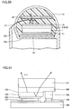
- this side-view type LED is equipped with a light emitting device (chip) fabricated according to the aforementioned fabricating method.
- Light emitting device 10 is placed such that the sides of the rectangular shape are lied horizontally.
- An Au line 31 is electrically connected to p-side pad electrode 22 placed at the center of the rectangular shape.
- the other end of Au line 31 is electrically connected to an electrode of a lead portion 32b protruded towards the light emitting surface.
- the n-electrode provided on the back surface of the GaN substrate is contacted with and electrically connected to a chip placing portion 32a of the lead frame.
- Lead frame 32 is provided with a concave-shaped reflective mirror for reflecting light emitted backward from the chip frontward.
- chip 10 is placed at the focal point of the concave-shaped curved surface.
- this side-view type LED is employed as a illumination light source of the display screen of a portable information terminal, the thickness or the height S will weigh.
- a conventional side-view type LED is equipped with a light emitting device of this comparison sample B.
- the laminated-layer construction of the light emitting device of comparison sample B is the same as that of invention sample A and is an n-type GaN layer 2/an n-type Al x Ga 1-x N layer 3/a multi quantum well layer (active layer) 4 consisting of (Al x Ga 1-x N/Al x In y Ga 1-x-y N) m /a p-type Al x Ga 1-x N layer 5/a p-type GaN layer 6 which have been formed on a sapphire substrate 101.
- the multi quantum well layer may be formed from (Ga x N/In x Ga 1-x N) m .
- the light emitting surface is surface 6a of p-type GaN layer 6 similarly to invention sample A and p-electrodes will be formed on this surface 6a.
- sapphire substrate 101 is an insulator, an n-electrode can not be provided on the sapphire substrate. Therefore, the edge portion of the laminate construction is cut away from surface 6a to the inside of n-type GaN layer 2 to expose n-type GaN layer 2 and then an n-electrode is provided on the exposed surface of n-type GaN layer 2.
- this side view type LED 130 is equipped with a light emitting device (chip) 110 fabricated according to the aforementioned fabricating method.
- Light emitting device 110 is placed such that the diagonal line of the rectangular shape is lied horizontally.
- An Au line 31 a is electrically connected to p-side pad electrode 22 placed at the center of the rectangular shape and an Au line 3 1b is electrically connected to n-electrode 111.
- the other end of Au line 31 a is electrically connected to an electrode (not shown) of a lead portion 32b of lead frame 32 which was protruded towards the light emitting surface.
- the other end of Au line 3 1b is electrically connected to an electrode of a chip mounting portion 32a of the lead frame.
- Lead frame 32 is provided with a concave-shaped reflective mirror for reflecting light emitted backward from the chip frontward.
- chip 10 is placed at the focal point of the concave-shaped curved surface.
- invention sample A and comparison sample B were mounted in an integrating-sphere in the state where a fluorescent material was not installed (but resin-sealing was applied) and then a predetermined current was applied thereto to cause light emission.
- the emitted light was collected by a detector and the light output values output from the detector are illustrated in Fig. 11 and Fig. 12.
- the light output value proportionally increases with increasing applied current.
- invention sample A and comparison sample B both generated an output of 8 mW.
- a fivefold current namely 100 mA
- comparison sample B generated an output of only 24 mW (Fig. 11).
- invention sample A had a relatively large heat generating area as compared with comparison sample B and therefore generated a smaller amount of heat per unit area for the same current injection (the current density in the MQW light emitting portion of invention sample A was 111 A/cm 2 , while the current density in the MQW light emitting portion of comparison sample B was 148 A/cm 2 , when the injected current was 100 mA).
- a GaN substrate having a heat conductivity higher than that of the sapphire substrate of comparison example B was employed.
- the n-electrode was provided on the N-surface side of the GaN substrate, which prevented the occurrences of portions having extremely high current densities.
- comparison sample B had a smaller heat radiating area than that of invention sample A. Furthermore, in comparison sample B, the n-electrode was formed on the exposed n-type GaN layer, and this significantly increased the density of currents flowing through the n-type GaN layer along the layer, which further increased the heat generation.
- the use of a GaN substrate having a relatively low dislocation density could improve the crystallinity of the epitaxially-grown films such as the MQW, which prevented reduction of the light emitting efficiency for large injected currents.
- the applied pulse current value was gradually changed with a duty ratio of 1% and the external quantum efficiency was calculated from the outputs.
- the result of the calculation is illustrated in Fig. 13.
- the external quantum efficiency of comparison sample B decreased with increasing current.
- the external quantum efficiency of invention sample A was substantially constant until the current reached 100 mA.
- comparison sample B can not generate high outputs at high currents, since such high outputs are caused by the crystallinity of the epitaxially-grown films formed on a substrate having a low dislocation density which is specific to invention sample A.
- invention sample A unlike comparison sample B, the n-electrode and the p-electrode are placed at the opposite positions and thus there is no possibility of electrical short-circuits.
- comparison sample B the n-electrode and the p-electrode are placed on the same side and therefore it may become necessary to provide a film for electrically insulating the p-electrode and the n-electrode from each other in order to prevent short-circuits therebetween.
- the invention sample does not require it, which may prevent additional increases in the manufacture cost.
- invention sample A can provide equivalent effects as compared with the comparison sample.
- an Al x Ga 1-x N substrate may be employed, instead of a GaN substrate, to provide similar effects, provided that it has equivalent characteristics as the substrate of a light emitting device.
- Fig. 14 and Fig. 15 illustrate the result of measurements of the luminance which is equivalent to the light output, for invention sample A and comparison sample B.
- invention sample A when a current of 100 mA was applied, invention sample A generated a luminance of 7.2 lm while comparison sample B generated a luminance of 4.3 lm.
- the invention sample can reduce the thickness and size of a side-view type LED lamp and provide higher outputs as compared with comparison sample B, even though the invention sample and comparison sample B have the same chip size. Even if an attempt is made to reduce the chip size of comparison sample B in order to reduce the thickness of the lamp, an etching space for forming the n-electrode and a fixed area of the p-pad electrode are required, and as a result, the opening ratio will be significantly decreased, which will prevent the generation of sufficient light outputs or luminances.
- the thickness of the side-view type LED can not be reduced to a value equivalent to that attained by invention sample A since there are the p-electrode at one of opposite corners of the chip and the n-electrode at the other comer, thereby requiring an additional space for wire bonding.
- electrostatic withstand voltage tests were performed for the aforementioned invention sample A and comparison sample B.
- the electrostatic withstand voltage tests were performed by placing the light emitting device and an electrostatically-charged condenser such that they were opposed to each other, then causing electric discharge therebetween and measuring the voltage therebetween when electric discharge was caused.
- the second embodiment of the present invention was characterized in that an invention sample C, an invention sample D and a comparison sample E were p-down-mounted and the back surface of the n-type layers or the n-type semiconductor substrate was used as a light emitting surface.
- Invention sample D had a dislocation density of 1E9/cm 2 , which was out of the range of dislocation density of light emitting devices according to the present invention employing a nitride semiconductor substrate having a reduced dislocation density.
- invention sample D was included in other types of light emitting devices according to the present invention.
- a sapphire substrate was employed to form comparison sample E and an attempt was made to provide an n-electrode and a p-electrode on the laminated-layers side of the sapphire substrate and down-mount these two electrode.
- an n-electrode having the same size as that of invention samples C, D could not be formed and therefore the fabrication thereof was discontinued. Comparisons were made mainly between invention sample C and invention sample D and thus influences of the dislocation density were examined.
- invention sample C and invention sample D both generated an output of 7 mW for an applied current of 20 A and generated an output of 17.5 mW and an output of 10.5 mW, respectively, for an applied current of 50 mA.
- invention sample C had a dislocation density about three orders of magnitude lower than that of invention sample D and because of the lower dislocation density, invention sample C could generate higher light emission outputs than those of invention sample D. Since invention sample C and invention sample D caused equivalent heat generation and heat radiation, this difference was not induced by influences of heat.
- invention sample C generated 1.26 1m for an applied current of 20 mA and 3.15 1m for an applied current of 50 mA
- invention sample D generated 1.26 1m for an applied current of 20 mA and 1.89 1m for an applied current of 50 mA.
- comparison sample E electrodes having the same diameter as those of invention samples A, C and comparison sample B, since there was not a space required for providing them as previously described. Even if the size of the exposed portion of the n-type GaN layer and the sizes of the n-electrode and the p-pad electrode are reduced and an n-electrode having the same size as that of invention samples C, D can be formed, there will be caused problems of heat generation at the electrodes, heat generation due to excessive current densities in the MQW and difficulty of ensuring the opening ratio of the p-electrode, which will prevent the generation of light outputs equivalent to those of invention sample C and invention sample D.
- performance such as the light output was examined for an invention sample F which was a light emitting device provided by applying a non-mirror-surface treatment to the aforementioned invention sample C and for a light emitting device provided with a reflective layer between the light emitting layer and the mounting portion (lead frame, etc.).
- a non-mirror-surface treatment has been applied to the back surface of the GaN substrate forming a light emitting surface and the side surfaces of the GaN surface and the side surfaces of the laminated-layer construction. Namely, the N-surface of the GaN substrate and the end surfaces of the device were made to be non-mirror surfaces.
- Fig. 21 illustrates an image of light being emitted from light emitting device 10 having mirror surfaces.
- the method for forming non-mirror surfaces there are methods using dry etching such as RIE or wet etching and methods using mechanical polishing.
- the present invention employed a method using wet etching with KOH solution as the etchant.
- KOH solution with a concentration of 4 mol/l (mol/dm 2 ) was sufficiently agitated with the temperature maintained at 40°C and then the wafer was immersed in the ultrasonic cleaning machine for 30 minutes to change the N-surface of the GaN substrate and the device end faces to mirror surfaces.
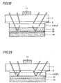
- the invention sample G is characterized in that a high reflective film 35 is placed under the p-electrode as illustrated in Fig. 22.
- a p-electrode 12 Ni with a thickness of 4 nm, Au with a thickness of 4 nm and Ag with a thickness of 100 nm were formed in order to form three laminated layers on p-type GaN layer 6 during the film formation (when mounted, it was p-down mounted and thus was upside-down). This was subjected to a heating process in an inert atmosphere to lower the contact resistance to 5E-4 ⁇ cm 2 .
- an Ni film with a thickness of 4 nm and an Au film with a thickness of 4 nm, as those in the aforementioned three-layers-electrode, were attached to a glass plate and then subjected to the same heating process. Then, the transmittance was measured. When incident light with a wavelength of 450 nm was directed thereto from the Ni side, the transmittance was 70%. Further, an Ag film with a thickness of 100 nm was attached to a glass plate and the reflectivity was measured. When incident light with a wavelength of 450 nm was directed thereto, the reflectivity was 88%.
- a Ni film with a thickness of 4 nm, an Au film with a thickness of 4 nm and an Ag film with a thickness of 100 nm were laminated in order on a glass plate to form a three-layers construction and then this three-layers construction was subjected to the aforementioned heating process. Then, the reflectivity was measured. When incident light with a wavelength of 450 nm was directed thereto, the reflectivity was 44%.
- This reflectivity agrees with the reflectivity calculated by assuming that the incident light with a wavelength of 450 nm passed through the Ni film with a thickness of 4 nm and the Au film with a thickness of 4 nm with a transmittance of 70%, then was reflected by the Ag layer with a reflectivity of 88% and then passed through the Ni film with a thickness of 4 nm and the Au film with a thickness of 4 nm with a transmittance of 70%, again.
- the invention sample H is characterized in that a high reflective film is placed under the p-electrode similarly to invention sample G illustrated in Fig. 22.
- a p-electrode 12 a Ni film with a thickness of 4 nm, an Au film with a thickness of 4 nm, an Al film with a thickness of 100 nm and an Au film with a thickness of 100 nm were formed in order on p-type GaN layer 6. This was subjected to a heating process in an inert atmosphere to lower the contact resistance to 5E-4 ⁇ cm 2 .
- a Ni film with a thickness of 4 nm, an Au film with a thickness of 4 nm and an Al film with a thickness of 100 nm were formed in this order on a glass plate to form a laminated-layers construction.
- this laminated-layers construction was subjected to the same heating process as the aforementioned heating process and then the reflectivity was measured.
- the reflectivity was 42% for incident light of 450 nm.
- This reflectivity agrees with the reflectivity calculated by assuming that the incident light with a wavelength of 450 nm passed through the Ni film with a thickness of 4 nm and the Au film with a thickness of 4 nm with a transmittance of 70%, then was reflected by the Al layer with a reflectivity of 42% and then passed through the Ni film with a thickness of 4 nm and the Au film with a thickness of 4 nm with a transmittance of 70%, again.
- the invention sample I is characterized in that a material Rh having a high reflectivity is employed for the p-electrode in invention sample C (see Fig. 23).
- a p-electrode 12 was formed by depositing Rh having a high reflectivity and a thickness of 100 nm on the entire surface of p-type GaN layer 6, the Rh being in ohmic-contact with the p-type GaN layer.
- the contact resistance was 5E-4 ⁇ cm 2 .
- Rh film as the p-electrode was deposited on a glass plate and the transmittance was measured.
- the transmittance was 60% for incident light of 450 nm.
- Invention samples F, G, H and I generated blue light of 8.1 mW, 8.4 mW, 8.4 mW and 9.1 mW for an applied current of 20 mA.
- Invention sample C including no reflective material generated 7 mW.
- the respective samples generated a luminance of 1.45 lm, 1.51 lm, 1.51 lm and 1.64 1m for an applied current of 20 mA.
- Invention sample C including no reflective material generated 1.26 lm.
- invention sample F having non-mirror surfaces
- invention sample I employing a high reflective material for the p-electrode could generate higher light outputs than invention sample C.
- KOH solution with a concentration in the range from 0.1 to 8 mol/l (mol/dm 3 ) and a temperature in the range from 20 to 80°C may be employed to provide equivalent effects.
- the reflective electrode will provide effects for any wavelength when the light emission wavelength is changed, even though the degree of effects can not be flatly described since the reflectivities of the Ag layer and the Al layer and the absorptances of the Au layer and the Ni layer will be changed. It is possible to employ, instead of Rh, an element having a work function and reflectivity equivalent to or more than those of Rh to provide effects equivalent to or more than those attained by Rh.
- nitride semiconductor substrates were employed and a GaN substrate and an AlxGa1-xN substrate having a reduced thickness were employed. Influences of the nitride semiconductor substrate were examined. In order to examine the characteristics of a side-view type LED lamp having a small thickness and a large lateral length, influences of the shape of the light emitting surface of the GaN substrate having a reduced thickness were examined.
- the invention sample J is characterized in that the thickness of the GaN substrate is reduced. Further, as will be described later, in addition to samples having a square light emitting surface, samples having a narrower light emitting surface were also examined.
- the invention sample K is characterized in that an Al x Ga 1-x N substrate is employed as a nitride semiconductor substrate.
- invention sample J a GaN substrate with a thickness of 100 ⁇ m
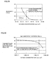
- measurements of the transmittance were performed for incident light with a wavelength of 380 nm as illustrated in Fig. 27A and Fig. 27B For invention sample J and invention sample K, measurements were performed for the two types of light emitting surfaces, namely 250 ⁇ m ⁇ and 250 ⁇ m ⁇ 1mm. As a result, as illustrated in Fig.
- invention sample J, invention sample K and comparison sample L equipped with no fluorescent material and resin-sealed, and invention sample J, invention sample K and comparison sample L equipped with a fluorescent material to be formed as white LEDs were mounted in an integrating-sphere and then a predetermined current was applied thereto. The emitted light was focused into a detector and then output from the detector. Comparisons of the light output values output from the detector and the luminances were performed.
- invention sample J, invention sample K and comparison sample L generated 4.2 mW (the luminance was 0.76 1m: for both the two types of light emitting device sizes), 5.4 mW (the luminance was 0.97 1m: for both the two types of light emitting device shapes and all the three types of x) and 0.6 mW (the luminance was 0.11 1m).
- the light outputs of invention sample J and invention sample K having a size of 250 ⁇ m ⁇ decreased with time due to influences of heat and these samples could not generate light outputs commensurate with the current.
- invention sample J having a size of 250 ⁇ m ⁇ ⁇ 1mm generated 50 mW (9.1 1m) which was 12 times that generated for an applied current of 20 mA
- invention sample K having a size of 250 ⁇ m ⁇ ⁇ 1 mm generated 64 mW (11.6 1m) which was 12 times that generated for an applied current of 20 mA.
- the difference in the light output for an applied current of 20 mA was caused by the difference in the transmittance of the substrate.
- a GaN substrate has an extremely low light transmittance for the short wavelength range shorter than 400 nm and therefore for the wavelength range shorter than 400 nm, the use of an Al x Ga 1-x N substrate enables extracting greater amounts of light. Further, reduction in the thickness of the GaN substrate also enables extracting greater amounts of light.
- excessively small thicknesses can not provide uniform light emission, which may prevent generating sufficient outputs, or concentrate light locally thereby locally degrading the resin. On the other hand, excessively large thicknesses will degrade the light extraction efficiency as previously described.
- the thickness is preferably 50 ⁇ m to 500 ⁇ m.
- the use of a GaN substrate having a small thickness as in the present embodiment reduces the manufacture cost of the GaN substrate, which enables the fabrication of low cost light emitting devices. It goes without saying that this results in reduction of the cost regardless of the light emission wavelength. Further, forming a light emitting surface of the chip with a rectangular shape as the invention samples having a size of 250 ⁇ m ⁇ ⁇ 1 mm enables increasing the area while maintaining the thickness S of the side-view type LED at a small value, namely 0.425 mm. This enables generating high outputs commensurate with the area. It goes without saying that the lager the substrate thickness set for uniformly spreading currents through the n-type layers, the larger the longitudinal size can be set, as previously described.
- Light emitting devices are based on that the relation between the oxygen concentration of the GaN substrate and the resistivity and light transmittance has been grasped.
- the sixth embodiment is characterized in that based on the relation, there was established the relation between optimal GaN substrate thicknesses and oxygen concentrations for a predetermined light emitting area for light emitting devices p-down mounted, namely light emitting devices in which the GaN substrate serves as the light emitting surface.
- the GaN substrate forms the light emitting surface, and therefore the oxygen concentration which largely affects the resistivity and the light transmittance will become particularly important.
- resistivities equal to or lower than 0.5 ⁇ cm can be realized by setting the oxygen concentration to 1E17/cm 3 or more.
- the oxygen concentration when the oxygen concentration is greater than 2E19/cm 3 , the transmittance for light with a wavelength of 450 nm sharply decreases.
- increasing the oxygen concentration is effective in reducing the resistivity of the GaN substrate and increasing the light emitting surface, but decreases the light transmittance. Therefore, for a GaN substrate for use in a light emitting device to be p-mounted, the setting of the oxygen concentration, the thickness and the light emitting plane size becomes significantly important.
- the oxygen concentration can be set to equal to or higher than 3E18/cm 3 (equal to or higher than 7E18/cm 3 for a square with a side length of 1mm) for a GaN substrate having a thickness of 50 ⁇ m to ensure light outputs equal to or higher than 7 mw with the size as of invention sample C for an applied current of 20 mA while generating uniform light emission.
- the applied current 20 mA for the size of invention sample C corresponds to an applied current of 125 mA (50 mA) for a square with a side length of 0.5 mm (a side length of 1mm).
- a current of 125 mA (500 mA) is applied thereto, light outputs equal to or greater than 44 mW (175 mW) can be ensured in proportion to the applied current, while uniform light emission can be achieved.
- the oxygen concentration can be set to equal to or higher than 1E18/cm 3 for a square with a side length of 0.5 mm (2E18/cm 3 for a square with a side length of 1 mm).
- the oxygen concentration must be set to a value equal to or lower than 1E19/cm 3 in order to provide light outputs equal to or higher than 7 mW with the size of invention sample C for an applied current of 20 mA.
- any oxygen concentration can not provide light equal to or higher than 7 mW with the size of invention sample C for an applied current of 20 mA, while oxygen concentrations equal to or greater than 5E17/cm 3 can provide uniform current flows through a square area with a side length of 0.5 mm.
- oxygen concentrations equal to or lower than 1E19/cm 3 can ensure light outputs equal to or higher than 6 mW with the size of invention sample C for an applied current of 20 mA , thereby preventing significant reduction in the light output while achieving uniform light emission.
- the GaN substrate has a thickness of 100 ⁇ m to 300 ⁇ m
- there is a practically sufficient oxygen concentration range which enables flowing currents uniformly through a square with a side length of 0.5 mm and also generating outputs equal to or higher than 7 mW with the size of invention sample C for an applied current of 20 mA.
- an oxygen concentration range from 2E18/cm 3 to 2E19/cm 3 enables that.
- an oxygen concentration range from 6E17/cm 3 to 5E18/cm 3 enables that.
- the GaN substrate has a thickness of 200 ⁇ m to 300 ⁇ m, there is also a practically sufficient oxygen concentration range which enables flowing currents uniformly through a square with a side length of 2 mm and also generating outputs equal to or higher than 7 mW with the size of invention sample C for an applied current of 20 mA.
- a GaN substrate having a thickness of 200 ⁇ m was employed wherein the GaN substrate had an oxygen concentration of 1E19/cm 3 and thus was n-typed.
- the GaN substrate had a resistivity of 0.007 ⁇ cm and a transmittance of 85% for light with a wavelength of 450 nm.
- the aforementioned GaN substrate was assembled into light emitting devices under the same conditions as those of aforementioned invention sample C except the aforementioned portion. Namely, the plane size of the GaN substrate was made to be a square such that the light emitting surface becomes a square with a side length of 0.2 mm (refer to (1) in the second embodiment).
- (a2) The following laminated-layer construction was formed on the Ga-surface, which was the first main surface, of the GaN substrate by MOCVD.
- a Si-doped N-type GaN layer/a Si-doped n-type Al 0.2 Ga 0.8 N layer being a clad layer/a MQW layer consisting of three layers each consisting of two layer construction comprised of a GaN layer and an In 0.15 Ga 0.85 N layer/a Mg-doped p-type Al 0.2 Ga 0.8 N layer being a clad layer/a Mg-doped p-type GaN layer).
- a GaN substrate with a thickness of 400 ⁇ m was employed wherein the GaN substrate had an oxygen concentration of 5E19/cm 3 and thus was n-typed.
- the GaN substrate had a resistivity of 0.002 ⁇ cm and a transmittance of 35% for light with a wavelength of 450 nm.
- the other conditions other than aforementioned portions were the same as those of invention sample S1.
- a GaN substrate with a thickness of 400 ⁇ m was employed wherein the GaN substrate had an oxygen concentration of 2E16/cm 3 and thus was n-typed.
- the GaN substrate had a resistivity of 1.0 ⁇ cm and a transmittance of 90% for light with a wavelength of 450 nm.
- the other conditions other than aforementioned portions were the same as those for invention sample S 1.
- test samples were assembled into p-down-mounted light emitting devices and a current of 20 mA was applied thereto.
- Invention sample S 1 generated a light output of 7 mW
- comparison sample T 1 and comparison sample T2 generated a light output of 2.9 mw and a light output of 5 mW, respectively. It can be said that the light output 2.9 mW of comparison sample T1 was an output commensurate with the transmittance of the GaN substrate.
- comparison sample T2 the condition of light emission was observed from the second main surface of the GaN substrate forming the light emission surface, and as a result, differences in the light emission intensity were found within the surface.
- the light emission intensity was extremely high around the n-electrode and the light emission intensity sharply decreased with increasing distance from the n-electrode. This was because the high resistivity of the GaN substrate prevented currents flowing through the n-electrode from sufficiently spreading through the surface of the light emitting device. This resulted in the occurrence of light emission only around the p-electrode where currents were concentrated. As a result, the light emission output from the entire light emitting device of comparison sample T2 was lower than that of invention sample S1.
- the seventh embodiment of the present invention is characterized in that the dislocation bundle density of the GaN substrate in a p-down mounted light emitting device was restricted to increase the light output.
- the dislocation bundle density of the GaN substrate in a p-down mounted light emitting device was restricted to increase the light output.
- the aforementioned dislocation bundles in the GaN substrate are transferred to p-type GaN layer 6 which is an epitaxial film and appear on the epitaxial film as cores 61 as illustrated in Fig. 32. Therefore, the dislocation bundle density is substantially in agreement with the core density.
- Cores 61 become hole-type concave portions as illustrated in Fig. 33, depending on the film forming condition of the epitaxial films. The density of hole-type concave portions drastically affects the fabrication yield of p-down-mounted light emitting devices in which the GaN substrate serves as the light emitting surface.
- a GaN substrate having dislocation bundles was employed, wherein a single dislocation bundle was distributed per 500 ⁇ m ⁇ 500 ⁇ m on average. This corresponds to a dislocation bundle density of 4E6/m 2 (4E2/cm 2 ). Other conditions were the same as those of invention sample S1.
- a GaN substrate having dislocation bundles was employed, wherein a single dislocation bundle was distributed per 10 ⁇ m ⁇ 10 ⁇ m. This corresponds to a dislocation bundle density of 1E10/m 2 (1E6/cm 2 ).
- Other conditions were the same as those of invention sample S2.
- the aforementioned GaN substrates were assembled into a plurality of light emitting devices on the basis of actual production.
- a current of 20 mA was applied to the respective test samples and the yield of light emitting devices capable of generating light outputs equal to or more than 7 mW was determined.
- invention sample S2 provided a yield of 97%
- comparison sample T3 provided a yield of 75%.
- dislocation bundle densities equal to or lower than 4E6/m 2 can provide yields which enable production.
- the dislocation bundle density exceeds the aforementioned density, it becomes impossible to continuously product light emitting devices on a commercial basis.
- Light emitting device which generated a light output lower than 7 mW were disassembled and the chips were extracted therefrom and examined.
- the electrodes were removed from the extracted chips using proper acid solution and the chips were examined from the p-type semiconductor side thereof.
- epitaxial films including portions which had not been grown at the portions of dislocation bundles in the GaN substrate.
- hole-type concave portions having a diameter of about 1 ⁇ m at the portions of the dislocation bundles. Such hole-type concave portions were not found in light emitting devices capable of generating light outputs equal to or higher than 7 mW.
- Comparison sample T3 had a light emitting surface with a size of 400 ⁇ m ⁇ , and therefore the yield was 75%. However, the inventors have discovered from experiments that when the chip size is 400 ⁇ m ⁇ , the yield is degraded to about 50%.
- the eighth embodiment (1) of the present invention is characterized in that an n-type AlGaN buffer layer and an n-type GaN buffer layer are placed between the GaN substrate and the n-type AlGaN clad layer 3.
- Substrates usually have warpage and GaN substrates have particularly large warpage. Therefore, GaN substrates have off angles which largely vary within the substrate surface, as illustrated in Fig. 34. Referring to Fig.
- the construction is divided into light emitting devices and then the light outputs of the light emitting devices are measured with the GaN substrate placed at the light emitting surface side (top side), light emitting devices formed on the region R1 lying at a comer and having a small off angle of 0.05° level and on the region R2 lying at a comer and having a large off angle of 1.5° level can not generate light outputs of 8 mW or higher for an applied current of 20 mA. This is because of the poor crystallinity of the epitaxial films formed on the GaN substrate. Therefore, as illustrated in Fig.
- n-type AlGaN buffer layer 71 having a lattice constant intermediate between those of the GaN substrate and AlGaN clad layer 3 and an n-type GaN buffer layer 2 between the GaN substrate and AlGaN clad layer 3, in order to alleviate the difference in the lattice constant. More specifically, the present embodiment is characterized in that n-type AlGaN buffer layer 71 is placed at the aforementioned position.
- a GaN substrate having off angles relative to the c-plane was employed, the off angles varying continuously from a region having an off angle of 0.05° to a region having an off angle of 1.5° within the surface of 20 mm ⁇ 20 mm, as illustrated in Fig. 34.
- the GaN substrate had a resistivity of 0.01 ⁇ cm, a dislocation density of 1E7/cm 3 and a thickness of 400 ⁇ m.
- light emitting devices were fabricated from respective portions of the aforementioned GaN substrate having a size of 20 mm ⁇ 20 mm according to the epitaxial-layer fabrication process for invention sample A of the first embodiment.
- an Al 0.15 Ga 0.85 N buffer layer having a thickness of 50 ⁇ m was placed between GaN substrate 1 and n-type GaN layer 2.
- a GaN substrate having off angles relative to the c-plane was employed, the off angles varying continuously from a region having an off angle of 0.05° to a region having an off angle of 1.5° within the surface of 20 mm ⁇ 20 mm.
- the GaN substrate had a resistivity of 0.01 ⁇ cm, a dislocation density of 1E7/cm 3 and a thickness of 400 ⁇ m.
- a plurality of light emitting devices were fabricated from respective portions of the GaN substrate according to the epitaxial-layer fabrication process for invention sample A of the first embodiment.
- an n-type GaN layer was formed on GaN substrate 1 and an Al 0.15 Ga 0.85 N buffer layer was not placed between the GaN substrate and the n-type GaN layer.
- invention sample S3 generated light outputs of 8 mW or more from the regions having off angles of 0.05 to 1.5° including the aforementioned regions R1, R2 in the GaN substrate having a size of 20 mm ⁇ 20 mm (see Fig.36).
- comparison sample T4 only light emitting devices formed on the regions having off angles from 0.1° to 1.0° could generate light output of 8 mW or more.
- the regions having off angle levels of 0.05° and 1.5° generated light outputs below 8 mW. This was because invention sample S3 included the Al 0.15 Ga 0.85 N buffer layer and this enabled formation of epitaxial layers having excellent crystallinity even though the GaN substrate with largely-varying off angles was employed.
- the eighth embodiment (2) is characterized in that an n-type AlGaN buffer layer and an n-type GaN buffer layer are placed between the GaN substrate and n-type AlGaN clad layer 3, similarly to the eighth embodiment (1), in order to eliminate hole-type concave portions as illustrated in Fig. 41 which generate when epitaxial films are formed on the portions of dislocation bundles in the GaN substrate as described in the tenth embodiment.
- a GaN substrate having a diameter of 2 inch and having dislocation bundles was employed, wherein one dislocation bundle was distributed per 10 ⁇ m ⁇ 10 ⁇ m. This corresponds to a dislocation bundle density of 1E6/cm 2 .
- an Al 0.15 Ga 0.85 N buffer layer having a thickness of 50 ⁇ m was placed between GaN substrate 1 and n-type GaN buffer layer 2.
- Other conditions were the same as those of invention sample S2.
- the epitaxial-layer-side surface of the wafer was observed with a differential interference microscope and SEM (Scanning Electron Microscope). As a result, no hole-type concave portion as in Fig. 41 was found.
- the entire GaN substrate having a diameter of 2 inch except the outer edge portion with a width of about 5 mm was assembled into light emitting devices. A single light emitting device was extracted from every 50 light emitting devices and a current of 20 mA was applied thereto. Thus, the yield of light emitting devices capable of generating a light output of 8 mW or more was determined. The resultant yield was 100%.
- the ninth embodiment is characterized in that a p-type AlGaN layer having an increased conductivity is placed outside of MQW 4/p-type AlGaN clad layer 5/p-type GaN layer 6, and an Ag electrode layer having a high reflectivity was placed over the entire surface as the p-electrode on the down side. Therefore, no other electrode is provided in consideration of the work function.
- the device has a high reflectivity at the down-side bottom portion, and this reduces light absorption which would occur in the case of using other metal electrodes, thereby increasing the light emitting efficiency.
- the following laminated-layer construction was formed on the Ga-surface, which is the first main surface, of a GaN substrate.
- (/MQW 4/Mg-doped p-type Al 0.2 Ga 0.8 N layer 5 being a clad layer/Mg-doped p-type GaN layer 6/a Mg-doped InGaN layer 72 with a thickness of 5 nm).
- the aforementioned laminated-layer construction is characterized in that a Mg-doped InGaN layer 72 with a thickness of 5 nm is provided in contact with Mg-doped p-type GaN layer 6. Further, in invention sample S4, an Ni/Au electrode layer was not formed as the p-electrode on the down side, and instead thereof an Ag layer 73 having a thickness of 100 nm was formed.
- An Ag electrode layer having a thickness of 100 nm was further placed on the Ni/Au electrode layer, as the p-electrode placed at the down side.
- Invention Sample S4 included p-type InGaN layer 72 in contact with p-type GaN layer 6 and therefore had a low acceptor level, thus increasing the carrier concentration. Therefore, even though Ag reflective film 73 having a work function which was not significantly high was placed in contact with p-type InGaN layer 72 as the p-electrode, the contact resistance between Ag reflective film 73 and p-type InGaN layer 72 was not significantly increased.
- the driving voltage of the light emitting device of invention sample S4 was compared with the driving voltage of the light emitting device of comparison sample T5. As a result, the difference therebetween was smaller than 0.05 V and thus no significant difference was noticed.
- Invention sample S4 generated a light output of 10.1 mW for an applied current of 20 mA, while comparison sample T5 generated 8.4 mW. Further, a lamp of the same construction as invention sample A (a GaN substrate and epitaxial laminated-layer construction) which was p-down mounted generated a light output of 7 mW.
- any material may be employed provided that the material has a high reflectivity and a contact resistance with p-type InGaN layer 72 which is not significantly large.
- Al or Rh may be employed.
- the tenth embodiment of the present invention is characterized in that Ni/Au layers having a low contact resistance with the p-type GaN layer were discretely placed and an Ag film is applied to fill the gaps, as the p-electrode at the down side, in order to increase the light output.
- Ni/Au electrode layers 12a are discretely placed with a predetermined pitch on the down-side bottom surface of the epitaxial layers.
- An Ag layer 73 is placed to fill the gaps and cover the down-side bottom surface of the epitaxial layers and Ni/Au electrode layers 12a at the down-side bottom surface of the epitaxial layers.
- a typical pitch of discrete Ni/Au electrode layers 12a is 3 ⁇ m.
- the pitch of 3 ⁇ m is based on that the diameter of the area in which currents spread is 6 ⁇ m at best in a typical p-type GaN layer or p-type AlGaN clad layer because of the resistivities. Namely, by setting the pitch to 3 ⁇ m, currents from a single discrete electrode reach the adjacent discrete electrodes. In order to flow currents through the electrode layers without causing discontinuity, it is preferable to set the pitch to below 3 ⁇ m. However, if the pitch is excessively small, the effective amount of extracted light will be reduced by the discretely-placed Ni/Au electrode layers.
- An epitaxial-laminated layer construction was fabricated according to the same fabrication process as that for invention sample C of the second embodiment.
- an Ni layer having a thickness of 4 nm was formed on the p-type GaN layer and then an Au layer having a thickness of 4 nm was formed on the entire surface thereof.
- patterning was applied thereto using a resist mask to form discretely-distributed Ni/Au electrodes (see Fig. 38 and Fig. 39). Then, this construction was subjected to a heating process in an inert gas atmosphere to change the contact resistance to 5E-4 ⁇ cm 2 .
- an Ag layer was formed over the entire surface to fill the gaps of the Ni/Au electrodes and cover the Ni/Au electrodes.
- the Ag layer was made as a reflective electrode.
- the area ratio of the discretely-distributed Ni/Au electrodes relative to the p-type GaN layer was 20% and the area ratio of Ag was 80%.
- the pitch of Ni/Au electrodes 12 was set to 3 ⁇ m (see Fig. 40).
- An epitaxial laminated-layer construction was fabricated on a GaN substrate according to the same fabrication process as that for invention sample C of the second embodiment.
- a p-electrode an Ni/Au layer was placed over the entire surface of the p-type GaN layer and then a heating process was applied thereto.
- an Ag layer was formed over the entire surface of the Ni/Au layer (see Fig. 41).
- Fig. 42 illustrates, for comparison, the behavior of reflection of light traveling toward the down side in a light emitting device of invention sample C.
- a current of 20 mA was applied to the respective light emitting devices fabricated as described above and the light outputs were measured.
- Invention sample S5 generated a light output of 10.1 mW
- comparison sample T6 generated 8.4 mW.
- the aforementioned ratio in comparison sample T6 was 67%.
- the aforementioned ratio in the light emitting device of invention sample C was 40% (Fig.42).
- comparison sample T6 belongs to the invention samples in a broad sense. Comparison sample T6 is merely defined as a comparison sample for convenience in order to describe the invention sample.
- Ni/Au electrode layers may be replaced with Pt electrode layers or Pd electrode layers.
- Ag reflective electrode layer may be replaced with a Pt layer or Pd layer.
- the invention sample generated higher light outputs than that of comparison sample T6 depending on the area ratio.
- the area ratio of the Ni/Au electrodes was 2%, which is lower than 10%
- the eleventh embodiment of the present invention is characterized in that a plurality of parallel plate-shaped crystal inversion regions propagated from the GaN substrate to the epitaxial layers are eliminated and the p-electrodes at the down side are placed at the respective gap regions of the plate-shaped crystal inversion regions.
- Plate-shaped crystal inversion regions are distributed in parallel to the thickwise direction of the GaN substrate and appear at the main surface of the GaN substrate in a stripe shape.
- the plate-shaped crystal inversion regions are propagated to epitaxial layers 2, 3, 4, 5, and 6.
- Fig. 43 and Fig. 44 illustrate plate-shaped crystal inversion regions placed in a lattice shape on the main surface.
- the present invention is characterized in that the aforementioned plate-shaped crystal inversion regions in the epitaxial layers are removed to a predetermined depth in the first main surface side to separate the respective epitaxial layers and p-electrodes are provided on the respective separated epitaxial layers (see Fig. 45).
- Plate-shaped crystal inversion regions may be lattice-shaped crystal inversion regions consisting of plate-shaped crystal inversion regions intersecting with each other on the main surface as illustrated in Fig. 43 or may be parallel plate-shaped crystal inversion regions which are aligned and distributed in a single direction on the main surface as will be described later. Plate-shaped crystal inversion regions are regions in which dislocations are concentrated with a high density.
- Plate-shaped crystal inversion regions are similar to dislocation bundles or cores 61 illustrated in Fig. 32. However, while dislocation bundles have a string shape or a wide line shape, plate-shaped crystal inversion regions 51 have a thickness and are placed in a plane shape.
- the first main surface at the epitaxial-layer side had a surface orientation of (0001) surface, namely the c-plane.
- the plate-shaped crystal inversion regions which were surface-symmetrical to the first main surface were (000-1) surface, namely the -c-plane, and the c-axis was grown in the reverse direction.
- the surface was a Ga-surface in which Ga atoms were arranged, while in the crystal inversion regions the surface was a N-surface in which N atoms were arranged.
- sample S6 a GaN substrate including crystal inversion regions having a width of 30 ⁇ m and arranged with a pitch of 100 ⁇ m on the first main surface was employed.
- the crystal inversion regions were propagated to the epitaxial layers formed on the GaN substrate.
- invention sample S6 was fabricated using the aforementioned GaN substrate, according to the same fabrication process as that of invention sample C.
- a mask pattern capable of covering only the crystal inversion regions which were propagated as illustrated in Fig. 44 was applied to the p-type GaN layer and p-electrode layers were fabricated only on the mask gap regions in the c-plane. Then, the mask pattern was removed.
- the aforementioned GaN substrate was held in 8N (normal) KOH at 80°C with a mask applied to the entire second main surface (back surface) to etch away the crystal inversion regions on the first main surface through the epitaxial layers such as the p-type GaN layer to the inside of the GaN substrate to form slots 52.
- Plate-shaped crystal inversion regions 51 were regions in which dislocations were concentrated with a high density and thus were easily etched by KOH.
- the etching depth in the GaN substrate was 150 ⁇ m from the boundary between the epitaxial layers and the GaN substrate inside the GaN substrate.
- the mask was removed and an insulating film was deposited to fill slots 52 (Fig. 45).
- the aforementioned invention sample S6 was assembled into a light emitting device and a current of 20 mA was applied thereto. As a result, the light emitting device generated a light output of 8.4 mW, which was 1.2 times the light output 7 mW of the light emitting device of invention sample C.
- plate-shaped crystal inversion regions are not required to have a lattice shape and may be plate-shaped crystal inversion regions arranged in parallel along a single direction on the main surface of the GaN substrate as illustrated in Fig. 46 and Fig. 47. Also, in the case of using a GaN substrate in which dot-shaped (actually, plane-shaped or small-round-shaped) crystal inversion regions are regularly placed, it is possible to generate light outputs higher than that of invention sample C similarly to invention sample S6, depending on the size and depth of the etching holes.
- the twelfth embodiment of the present invention is characterized in that a fluorescent plate 46 is placed above the semiconductor chip such that it faces with GaN substrate 1 and further this construction is sealed with a resin 15. There is a novelty in that the fluorescent plate is placed such that it faces with the GaN substrate serving as the emitting surface in the p-down mounted construction.
- Invention samples S7 and S8 illustrated in Fig. 48 and comparison sample T7 were utilized as test samples.
- Fluorescent plate 46 was fabricated with the following fabrication method. A bulk-shaped ZnSSe crystal in which I (iodine) had been diffused by halogen transfer was fabricated and then this bulk-shaped ZnSSe crystal was heated in an atmosphere of Zn, Cu to diffuse Cu into the ZnSSe. Subsequently, this bulk ZnSSe crystal was polished to a thickness of 0.5 mm using a rough polishing disc and then cut into a shape which can be accommodated in the lead frame. The surface and the back surface of the fluorescent plate fabricated with the aforementioned method had a roughness R max of 1 ⁇ m.
- invention sample S8 asperities were formed on surface 46a of fluorescent plate 46 to be faced with the GaN substrate (see Fig. 49).
- the height of asperities was set to 2 ⁇ m and the pitch of the asperities was set to 5 ⁇ m on average.
- the other constructions were the same as those of invention sample S7.
- a fluorescent plate 46 was placed above the chip which was p-top mounted such that it faced with the chip and further the chip was sealed with an epoxy resin 15 to form a white light emitting device.
- the aforementioned GaN substrate is n-typed with oxygen-doping and has an oxygen concentration of 1E17 to 2E19 oxygen atoms/cm 3 and a thickness of 100 ⁇ m to 600 ⁇ m.
- the resistivity of the GaN substrate can be increased and therefore currents introduced from the p-electrode can be sufficiently spread through the GaN substrate, which enables sufficiently utilizing the width of the active layer to cause light emission.
- a transmittance equal to or higher than 60% can be ensured for light with a wavelength of 450 nm, thereby increasing the transmittance of the GaN substrate which serves as the light emitting surface. This enables ensuring the light output.
- the aforementioned oxygen concentration range is particularly effective for the GaN substrate thickness range from 100 ⁇ m to 600 ⁇ m.
- the aforementioned oxygen concentration may be in the range from 2E18 to 5E18 oxygen atoms/cm 3 and the thickness of the GaN substrate may be in the range from 100 ⁇ m to 600 ⁇ m.
- the both side lengths of the rectangular-shaped surface of the light emitting surface at the aforementioned second main surface may be equal to or smaller than 0.5 mm.
- This configuration enables causing light emission over the entire light emitting surface and also generating sufficient light outputs.
- the aforementioned oxygen concentration may be in the range from 3E18 to 5E18 oxygen atoms/cm 3 and the thickness of the GaN substrate may be in the range from 200 ⁇ m to 300 ⁇ m.
- the both side lengths of the rectangular-shaped light emitting surface at the aforementioned second main surface may be equal to or smaller than 2 mm and the both side lengths of the rectangular-shaped surface of the light emitting surface at the aforementioned second main surface may be equal to or smaller than 0.5 mm.
- This configuration enables causing light emission over the entire light emitting surface and also generating sufficient light outputs, even when the chip size is increased to 2 mm ⁇ at maximum.
- a GaN substrate having dislocation bundles distributed over the first main surface of the GaN substrate with a density equal to or lower than 4E6/cm 3 on average may be employed, wherein the dislocation bundles have been created by discretely concentrating dislocations which unavoidably generate during the formation of the GaN substrate into a string shape to distribute them along the substrate thickness direction in order to improve the crystallinity of the most region of the aforementioned GaN substrate.
- This configuration enables fabrication of light emitting devices capable of generating light outputs equal to or higher than a predetermined value with a high fabrication yield.
- the aforementioned dislocation bundles are distributed with a density equal to or lower than 4E2/cm 2 on average on the first main surface and the shorter side length of the light emitting surface at the aforementioned second main surface may be in the range from 200 ⁇ m to 400 ⁇ m.
- a miniaturized light emitting device as described above includes dislocation bundles
- the performance of the device will be unavoidably degraded, thereby directly resulting in reduction in the yield.
- the reduction in the yield can be restricted to a practically acceptable range.
- an n-type AlGaN buffer layer is placed in contact with the GaN substrate, an n-type GaN buffer layer is placed in contact with the n-type AlGaN buffer layer and the n-type Al x Ga 1-x N layer (x is in the range from 0 to 1) may be placed in contact with the n-type GaN buffer layer.
- an n-type AlGaN buffer layer and an n-type GaN buffer layer may be placed between the GaN substrate and the n-type Al x Ga 1-x N layer (x is in the range from 0 to 1) which is a clad layer for the active layer.
- n-type AlGaN buffer layer as well as the n-type GaN buffer layer between the GaN substrate and the clad layer, a hetero-epitaxial laminate-layer construction with an excellent crystallinity can be formed.
- the aforementioned laminated-layer construction may be advantageously employed particularly in the case where the GaN substrate includes a region with an off angle equal to or lower than 0.10° and a region with an off angle equal to or greater than 1.0°.
- a p-type GaN buffer layer may be placed in contact with the aforementioned p-type Al x Ga 1-x N layer (x is in the range from 0 to 1) at the down side thereof and a p-type InGaN contact layer may be placed in contact with the p-type GaN buffer layer.
- a p-type InGaN contact layer with an excellent electrical conductivity may be placed under the p-electrode layer, and this decreases the necessity of selecting the material of the p-electrode layer in consideration of the work function. This enables selecting the material of the p-electrode in consideration of the reflectivity, for example.
- the aforementioned p-type InGaN contact layer may have a Mg concentration in the range of 1E18 atoms/cm 3 to 1E21 atoms/cm 3 .
- a p-electrode layer consisting of an Ag layer may be provided in contact with the aforementioned p-type InGaN contact layer.
- the reflectivity at the bottom of the light emitting device namely the mounting portion can be increased to reduce the light loss, thereby increasing the light output.
- the aforementioned GaN substrate may include plate-type crystal inversion regions extending continuously in the thickwise direction and over the GaN substrate surface.
- the plate-type crystal inversion regions in the GaN substrate and plate-type crystal inversion regions propagated through the n-type and p-type nitride semiconductor layers formed on the GaN substrate are removed from the p-type nitride semiconductor layers to the GaN substrate through the n-type nitride semiconductor layers.
- p-electrodes may be provided for the respective portions of the p-type nitride semiconductor layers.
- the light extracting surface can be widened to increase the light output.
- First electrodes may be placed over the surface of the p-type nitride semiconductor layers in contact with the p-type nitride semiconductor layers and a second electrode formed from Ag may be provided such that the second electrode fills the gaps of the first electrodes and covers the p-type nitride semiconductor layers and the first electrodes.
- This configuration enables sufficiently spreading currents introduced from the p-electrodes over the surface while increasing the reflectivity, thereby increasing the light output.
- the coverage ratio of the aforementioned discretely-placed first p-electrodes relative to the surface of the p-type nitride semiconductor layers may be in the range from 10 to 40%.
- This configuration enables sufficiently spreading introduced currents over the surface while ensuring the electrical conductivity. Coverage ratios lower than 10% can not enables flowing currents through the epitaxial layers without causing discontinuity. Also, with coverage ratios higher than 40%, the adverse effects of the discretely-placed p-electrodes on the light extracting efficiency can not be neglected.
- a fluorescent plate may be placed apart from the aforementioned nitride semiconductor substrate such that it faces with the second main surface of the nitride semiconductor substrate.
- the surface of the fluorescent plate to be faced with the second main surface of the nitride semiconductor substrate may be subjected to an asperities-forming process.
- the aforementioned configuration can further increase the light extracting efficiency.
- the aforementioned light emitting device may be sealed with resin and may include a fluorescent member at any portion of the light emitting device and any portion of the resin.
- the fluorescent member generates fluorescence on receiving light and thus white light will be emitted from the resin to the outside.
- This configuration enables easily providing a white light emitting device having the aforementioned advantages of the present invention.
- a single electrode at the top side may be placed at the center of the light emitting device, in a plane view of the respective layers.
- the aforementioned configuration enables providing a sufficient space for wire bonding. Further, in the case of constructing a side-view type LED, the configuration can reduce the thickness of the side-view type LED.
- the aforementioned light emitting device may be constructed such that a side-view type LED equipped with the light emitting device will have a thickness equal to or smaller than 0.5 mm or equal to or smaller than 0.4 mm.
- the aforementioned light emitting device may have an electrostatic withstand voltage of 3000 V or more.
- This configuration provides durability with respect to surge voltage from the outside, thereby maintaining stabled and high performance. Further, this configuration eliminates the necessity of providing a protection device for protecting the light emitting devise from the surge voltage from the outside. Namely, there is no need to provide a protection circuit for protecting the light emitting device from transient voltages or electrostatic discharge, which would be otherwise applied between the aforementioned nitride semiconductor substrate and the p-type nitride semiconductor layers. More specifically, there is no need to provide an electric power shunting circuit including Zener diodes for dealing with such transient voltages or electrostatic discharge.
- the aforementioned light emitting device may be constructed to cause light emission when a voltage of 4 V is applied thereto.
- a nitride semiconductor substrate having a high electrical conductivity and thus having a low electrical resistance enables injecting a sufficient current to cause light emission with a low applied voltage to cause light emission. This reduces the number of batteries to be mounted, thereby contributing reduction in the size, weight and cost of an illumination apparatus equipped with the light emitting device. Further, this is effective in saving the power consumption.
- the aforementioned nitride semiconductor substrate may have a thickness in the range from 50 ⁇ m to 500 ⁇ m.
- the GaN substrate or n-type nitride semiconductor substrate has a large thickness. If the aforementioned substrate has a thickness smaller than 50 ⁇ m, when the n-electrode has a small area, electrons can not sufficiently spread when they reach the active layer, which induces portions in the active layer which generate insufficient light emission or no light emission.
- the thickness of the aforementioned substrate By setting the thickness of the aforementioned substrate to 50 ⁇ m or more, currents sufficiently spread within the aforementioned substrate because of the low electric resistivity, thereby sufficiently increasing the light emitting portion in the active layer, even when the n-electrode has a small area. More preferably, the thickness is 75 ⁇ m or more. However, when the thickness is excessively large, the absorption at the substrate can not be neglected. Therefore, the thickness must be equal to or smaller than 500 ⁇ m. The thickness is preferably equal to or smaller than 400 ⁇ m and more preferably equal to or smaller than 3 00 ⁇ m.
- the aforementioned electrode at the top side has an area ratio below 50% and therefore the opening ratio or the transparent portion is higher than 50%.
- This configuration can increase the emitting efficiency of light from the light emitting surface.
- the greater the opening ratio the smaller the amount of light absorbed by the n-electrode and thus the higher the light output. Therefore, the opening ratio is preferably 75% and more preferably 90%.
- At least one of the sides of the aforementioned top-side surface may have a length of 350 ⁇ m. This configuration can reduce the height of the side-view type LED to below 0.5 mm.
- At least one of the sides of the aforementioned top-side surface may have a length of 250 ⁇ m. This configuration can reduce the height of the side-view type LED to below 0.4 mm.
- the aforementioned configuration can lengthen the light emitting surface while maintaining the distance between opposite sides of the rectangular shape at a fixed length, resulting in increased area and increased light output.
- the length in the longer side direction can be set to 1.6 mm or smaller.
- the aforementioned heat resistance may be equal to or lower than 30 °C/W.
- the light emitting efficiency of the light emitting device is degraded by temperature rises. Further, excessive temperature rises will damage the light emitting device. Therefore, the temperature resistance or heat resistance is an important design factor.
- the heat resistance has been set to 60 °C/W (the aforementioned patent literature 1). However, as previously described, by setting the heat resistance to 30 °C/W or less, it is possible to prevent reduction in the light emitting efficiency or damage of the light emitting device, even when sufficient electric power is introduced into the light emitting device.
- the half-reduction of the heat resistance was realized by using a GaN substrate having a low resistivity as previously described.
- portion at which temperature rises most largely may have a temperature equal to or lower than 150°C under continuous light emitting conditions.
- the temperature at the portion at which temperature rises most largely namely the light emitting layer, can be set to below 150°C, thereby ensuring a sufficiently high light emitting efficiency. Further, the life can be largely lengthened as compared with conventional light emitting devices.
- the thickness of the aforementioned n-type nitride semiconductor layers may be set to 3 ⁇ m or less.
- the n-type nitride semiconductor layers are epitaxially grown on the nitride semiconductor substrate. Therefore, if the thickness of the n-type nitride semiconductor layers is excessively large, the film forming process will require long time and also the material cost will be increased. By setting the thickness of the n-type nitride semiconductor layers to 3 ⁇ m or less, the cost can be significantly decreased. More preferably, the thickness is set to 2 ⁇ m or less.
- the aforementioned p-type nitride semiconductor layers are down-mounted, and the portion of the second main surface (back surface) of the aforementioned nitride semiconductor surface which has not been covered with the electrode may have been subjected to a non-mirror-surface treatment.
- This configuration can prevent light generated at the light emitting layer from being totally reflected at the second main surface, or the emitting surface, to be confined within the aforementioned substrate, thus reducing the efficiency. It goes without saying that the side surfaces of the laminated-layer construction may be subjected to the non-mirror-surface treatment.
- the aforementioned surfaces which have been subjected to the non-mirror-surface treatment may be surfaces which were made to be non-mirror surfaces using potassium hydroxide (KOH) solution, sodium hydroxide (NaOH) solution, ammonia (NH 3 ) solution or other alkali solution.
- KOH potassium hydroxide
- NaOH sodium hydroxide
- NH 3 ammonia
- the N-surface of the GaN substrate may be efficiently made to be a surface with asperities.
- the Ga-surface side is not etched.
- the aforementioned surfaces which have been subjected to the non-mirror-surface treatment may be surfaces which were made to be non-mirror surfaces using at least one of sulfuric acid (H 2 SO 4 ) solution, hydrochloric acid (HCl) solution, phosphoric acid (H 2 PO 4 ) solution, hydrofluoric acid (HF) solution and other acid solution.
- sulfuric acid H 2 SO 4
- hydrochloric acid HCl
- phosphoric acid H 2 PO 4
- HF hydrofluoric acid
- the aforementioned surfaces which have been subjected to the non-mirror-surface treatment may be surfaces which were made to be non-mirror surfaces using reactive ion etching: RIE). Therefore, non-mirror surfaces with an excellent area dimension accuracy can be provided with a dry process. Also, by combining photolithography technique with RIE which is a dry etching or wet etching using alkali solution, predetermined asperities intervals can be provided.
- RIE reactive ion etching
- the electrode placed on the mounting-surface side may be formed from a material with a reflectivity equal to or higher than 0.5.
- This configuration can prevent absorption of light at the mounting-surface side and increase the amount of light reflected toward the second main surface of the aforementioned substrate. It is desirable that this reflectivity is higher and is equal to or higher than 0.7.
- a fluorescent member may be placed such that it covers the second main surface of the aforementioned nitride semiconductor substrate.
- the nitride semiconductor substrate may include at least one of impurities and defects which generate fluorescence.
- the aforementioned configuration enables forming a white light emitting LED.
- the light emitting device of the present invention may include more than one aforementioned configuration of a light emitting device and these configurations of a light emitting device may be connected in serial.
- the aforementioned configuration enables providing an illumination apparatus equipped with a plurality of the aforementioned high efficiency light emitting devices mounted on a lead frame, by utilizing a high current power supply.
- the light emitting device of the present invention may include more than one aforementioned configuration of a light emitting device and these configurations of a light emitting device may be connected in parallel.
- the aforementioned configuration enables providing an illumination apparatus constituted by the aforementioned high efficiency light emitting devices, by utilizing a high current power supply.
- An illumination apparatus may include light emitting devices of the present invention and a power supply circuit for causing the light emitting devices to generate light and in the power supply circuit, two or more parallel portions each including two or more light emitting devices connected in parallel are connected in parallel.
- the aforementioned power supply circuit may include a parallel/serial switching portion when the capacity of the illumination apparatus is made variable, and the wiring to be applied to the light emitting devices may be switched through the parallel/serial switching portion.
- the light emitting device of the present invention employs a nitride semiconductor substrate having a high conductivity and therefore, regardless of p-down mounted or n-down mounted, (1) only a single electrode can be provided on the light emitting surface. Further, (2) by employing the aforementioned nitride semiconductor substrate with a high conductivity and also by p-down mounting, a miniaturized light emitting device can be provided. Further, in the case of p-down mounting, (3) the heat radiation can be improved, there is no need to provide a complicated electrode configuration and further higher output light emission can be generated. (4) The conductivity is improved and there is no need to provide protection circuit for protecting the light emitting device from transient voltages or electrostatic discharge.
- the light emitting device Since there is no significant discontinuity in the refractive index from the light emitting layer to the substrate, light is less prone to be totally reflected, thereby preventing efficiency reduction and resin degradation at the side surface, which would be otherwise caused by total reflection. (6) Since the construction is simplified, the light emitting device is easy to manufacture and has an excellent maintainability. Therefore, it is expected that the light emitting device will be widely utilized in the illumination apparatuses of portable information terminals including portable phones.
Landscapes
- Led Devices (AREA)
- Led Device Packages (AREA)
Applications Claiming Priority (4)
| Application Number | Priority Date | Filing Date | Title |
|---|---|---|---|
| JP2003404266 | 2003-12-03 | ||
| JP2003404266 | 2003-12-03 | ||
| JP2004279980 | 2004-09-27 | ||
| JP2004279980A JP2005191530A (ja) | 2003-12-03 | 2004-09-27 | 発光装置 |
Publications (2)
| Publication Number | Publication Date |
|---|---|
| EP1538680A2 true EP1538680A2 (fr) | 2005-06-08 |
| EP1538680A3 EP1538680A3 (fr) | 2011-10-05 |
Family
ID=34467843
Family Applications (1)
| Application Number | Title | Priority Date | Filing Date |
|---|---|---|---|
| EP04028630A Withdrawn EP1538680A3 (fr) | 2003-12-03 | 2004-12-02 | Dispositf électroluminescent |
Country Status (8)
| Country | Link |
|---|---|
| US (1) | US7190004B2 (fr) |
| EP (1) | EP1538680A3 (fr) |
| JP (1) | JP2005191530A (fr) |
| KR (1) | KR100955634B1 (fr) |
| CN (1) | CN1624944B (fr) |
| CA (1) | CA2488596A1 (fr) |
| SG (1) | SG112077A1 (fr) |
| TW (1) | TWI351773B (fr) |
Cited By (22)
| Publication number | Priority date | Publication date | Assignee | Title |
|---|---|---|---|---|
| EP1697983A4 (fr) * | 2003-12-09 | 2008-04-23 | Univ California | Diodes electroluminescentes a base de nitrure de gallium tres efficaces grace a une surface rendue rugueuse |
| US7491974B2 (en) | 2005-06-13 | 2009-02-17 | Sumitomo Electric Industries, Ltd. | Light-emitting device |
| EP2159475A1 (fr) * | 2008-08-28 | 2010-03-03 | T.Y.C. Brother Industrial Co., Ltd. | Dispositif d'illumination |
| EP1946389A4 (fr) * | 2005-11-09 | 2010-12-29 | Alti Electronics Co Ltd | Del de type a vue laterale et son procede de fabrication |
| EP2136414A4 (fr) * | 2007-03-26 | 2011-08-03 | Nichia Corp | Dispositif électroluminescent |
| WO2012026966A1 (fr) * | 2010-08-25 | 2012-03-01 | Cree, Inc. | Boîtier émetteur doté de del en biais ou verticales |
| USD671661S1 (en) | 2008-01-10 | 2012-11-27 | Cree Hong Kong Limited | LED package |
| EP1929549A4 (fr) * | 2005-09-26 | 2012-12-26 | Showa Denko Kk | Procédé de fabrication d'un dispositif émetteur de lumière semi-conducteur au nitrure |
| US8362605B2 (en) | 2006-04-26 | 2013-01-29 | Cree Huizhou Opto Limited | Apparatus and method for use in mounting electronic elements |
| US8367945B2 (en) | 2006-08-16 | 2013-02-05 | Cree Huizhou Opto Limited | Apparatus, system and method for use in mounting electronic elements |
| US8368112B2 (en) | 2009-01-14 | 2013-02-05 | Cree Huizhou Opto Limited | Aligned multiple emitter package |
| US8564004B2 (en) | 2011-11-29 | 2013-10-22 | Cree, Inc. | Complex primary optics with intermediate elements |
| US8669572B2 (en) | 2005-06-10 | 2014-03-11 | Cree, Inc. | Power lamp package |
| US8735920B2 (en) | 2006-07-31 | 2014-05-27 | Cree, Inc. | Light emitting diode package with optical element |
| US8791471B2 (en) | 2008-11-07 | 2014-07-29 | Cree Hong Kong Limited | Multi-chip light emitting diode modules |
| US9012938B2 (en) | 2010-04-09 | 2015-04-21 | Cree, Inc. | High reflective substrate of light emitting devices with improved light output |
| US9035439B2 (en) | 2006-03-28 | 2015-05-19 | Cree Huizhou Solid State Lighting Company Limited | Apparatus, system and method for use in mounting electronic elements |
| US9070850B2 (en) | 2007-10-31 | 2015-06-30 | Cree, Inc. | Light emitting diode package and method for fabricating same |
| US9601670B2 (en) | 2014-07-11 | 2017-03-21 | Cree, Inc. | Method to form primary optic with variable shapes and/or geometries without a substrate |
| US9711703B2 (en) | 2007-02-12 | 2017-07-18 | Cree Huizhou Opto Limited | Apparatus, system and method for use in mounting electronic elements |
| EP2190038B1 (fr) * | 2008-11-25 | 2020-01-01 | LG Innotek Co., Ltd. | Dispositif électroluminescent à semi-conducteur |
| US10622522B2 (en) | 2014-09-05 | 2020-04-14 | Theodore Lowes | LED packages with chips having insulated surfaces |
Families Citing this family (136)
| Publication number | Priority date | Publication date | Assignee | Title |
|---|---|---|---|---|
| USD536672S1 (en) * | 2002-09-05 | 2007-02-13 | Nichia Corporation | Light emitting diode |
| USD537047S1 (en) * | 2002-09-05 | 2007-02-20 | Nichia Corporation | Light emitting diode |
| US9142734B2 (en) * | 2003-02-26 | 2015-09-22 | Cree, Inc. | Composite white light source and method for fabricating |
| CN100502062C (zh) | 2003-04-30 | 2009-06-17 | 美商克立股份有限公司 | 具有小型光学元件的高功率发光器封装 |
| US7005679B2 (en) | 2003-05-01 | 2006-02-28 | Cree, Inc. | Multiple component solid state white light |
| JP3841092B2 (ja) * | 2003-08-26 | 2006-11-01 | 住友電気工業株式会社 | 発光装置 |
| JP4116985B2 (ja) * | 2004-07-26 | 2008-07-09 | 松下電器産業株式会社 | 発光装置 |
| USD531966S1 (en) * | 2004-10-18 | 2006-11-14 | Rohm Co., Ltd. | Light emitting diode |
| USD538240S1 (en) * | 2004-10-18 | 2007-03-13 | Rohm Co., Ltd. | Package for light emitting diode |
| USD532382S1 (en) * | 2004-10-18 | 2006-11-21 | Rohm Co., Ltd. | Package for light emitting diode |
| USD526971S1 (en) * | 2004-10-18 | 2006-08-22 | Rohm Co., Ltd. | Light emitting diode |
| USD540269S1 (en) * | 2004-10-18 | 2007-04-10 | Rohm Co., Ltd. | Package for light emitting diode |
| USD526970S1 (en) * | 2004-10-18 | 2006-08-22 | Rohm Co., Ltd. | Light emitting diode |
| USD529877S1 (en) * | 2004-10-18 | 2006-10-10 | Rohm Co., Ltd. | Light emitting diode |
| USD534876S1 (en) * | 2004-10-18 | 2007-01-09 | Rohm Co., Ltd. | Package for light emitting diode |
| USD533517S1 (en) * | 2004-12-27 | 2006-12-12 | Samsung Electro-Mechanics Co., Ltd. | Light-emitting diode |
| JP2006202845A (ja) * | 2005-01-18 | 2006-08-03 | Sony Corp | 半導体発光装置 |
| USD534132S1 (en) * | 2005-03-23 | 2006-12-26 | Seoul Semiconductor Co. Ltd. | Light emitting diode (LED) |
| USD529452S1 (en) * | 2005-04-08 | 2006-10-03 | Seoul Semiconductor Co. Ltd. | Light emitting diode (LED) |
| USD529451S1 (en) * | 2005-05-13 | 2006-10-03 | Seoul Semiconductor Co. Ltd. | Light emitting diode (LED) |
| US9153645B2 (en) | 2005-05-17 | 2015-10-06 | Taiwan Semiconductor Manufacturing Company, Ltd. | Lattice-mismatched semiconductor structures with reduced dislocation defect densities and related methods for device fabrication |
| US8324660B2 (en) | 2005-05-17 | 2012-12-04 | Taiwan Semiconductor Manufacturing Company, Ltd. | Lattice-mismatched semiconductor structures with reduced dislocation defect densities and related methods for device fabrication |
| KR100638819B1 (ko) * | 2005-05-19 | 2006-10-27 | 삼성전기주식회사 | 광추출효율이 개선된 수직구조 질화물 반도체 발광소자 |
| JP2007027431A (ja) * | 2005-07-15 | 2007-02-01 | Toshiba Corp | 発光装置 |
| US8674375B2 (en) | 2005-07-21 | 2014-03-18 | Cree, Inc. | Roughened high refractive index layer/LED for high light extraction |
| USD528998S1 (en) * | 2005-07-22 | 2006-09-26 | Samsung Electro-Mechanics Co., Ltd. | Light-emitting diode |
| USD538760S1 (en) * | 2005-07-22 | 2007-03-20 | Samsung Electro-Mechanics Co., Ltd. | Light-emitting diode |
| US7675897B2 (en) * | 2005-09-06 | 2010-03-09 | Current Technologies, Llc | Power line communications system with differentiated data services |
| WO2007029744A1 (fr) * | 2005-09-06 | 2007-03-15 | Japan Science And Technology Agency | Semi-conducteur de nitrure de groupe iii/v, élément semi-conducteur photocatalytique, appareil de réaction redox photocatalytique, et procédé d’exécution de réaction photoélectrochimique |
| USD549187S1 (en) * | 2006-01-09 | 2007-08-21 | Alti-Electronics Co., Ltd. | Light emitting diode (LED) package |
| US7777250B2 (en) | 2006-03-24 | 2010-08-17 | Taiwan Semiconductor Manufacturing Company, Ltd. | Lattice-mismatched semiconductor structures and related methods for device fabrication |
| US8357243B2 (en) | 2008-06-12 | 2013-01-22 | Sixpoint Materials, Inc. | Method for testing group III-nitride wafers and group III-nitride wafers with test data |
| WO2012135976A1 (fr) * | 2011-04-07 | 2012-10-11 | Cree Huizhou Solid State Lighting Company Limited | Dispositif de diode électroluminescente ayant une émission de pic inclinée et dispositif d'affichage à diodes électroluminescentes comprenant de tels dispositifs |
| CN102437152A (zh) * | 2006-04-24 | 2012-05-02 | 克利公司 | 侧视表面安装式白光led |
| US8487326B2 (en) * | 2006-04-24 | 2013-07-16 | Cree, Inc. | LED device having a tilted peak emission and an LED display including such devices |
| US11210971B2 (en) | 2009-07-06 | 2021-12-28 | Cree Huizhou Solid State Lighting Company Limited | Light emitting diode display with tilted peak emission pattern |
| KR100735496B1 (ko) * | 2006-05-10 | 2007-07-04 | 삼성전기주식회사 | 수직구조 질화갈륨계 led 소자의 제조방법 |
| KR100820529B1 (ko) | 2006-05-11 | 2008-04-08 | 엘지이노텍 주식회사 | 발광 장치 및 그 제조방법, 면 발광 장치 |
| JP5250856B2 (ja) * | 2006-06-13 | 2013-07-31 | 豊田合成株式会社 | 窒化ガリウム系化合物半導体発光素子の製造方法 |
| WO2007149487A2 (fr) * | 2006-06-21 | 2007-12-27 | The Regents Of The University Of California | Dispositifs optoélectroniques et électroniques utilisant des substrats gan à n faces ou à m plans préparés par croissance ammoniothermique |
| KR100816841B1 (ko) | 2006-08-14 | 2008-03-26 | 삼성전기주식회사 | 수직구조 질화갈륨계 발광다이오드 소자 및 그 제조방법 |
| KR100769727B1 (ko) * | 2006-08-17 | 2007-10-23 | 삼성전기주식회사 | 표면 요철 형성방법 및 그를 이용한 질화갈륨계발광다이오드 소자의 제조방법 |
| US7800122B2 (en) * | 2006-09-07 | 2010-09-21 | Hong Kong Applied Science And Technology Research Institute Co., Ltd. | Light emitting diode device, and manufacture and use thereof |
| US8173551B2 (en) | 2006-09-07 | 2012-05-08 | Taiwan Semiconductor Manufacturing Co., Ltd. | Defect reduction using aspect ratio trapping |
| US20100224890A1 (en) * | 2006-09-18 | 2010-09-09 | Cree, Inc. | Light emitting diode chip with electrical insulation element |
| US7875958B2 (en) | 2006-09-27 | 2011-01-25 | Taiwan Semiconductor Manufacturing Company, Ltd. | Quantum tunneling devices and circuits with lattice-mismatched semiconductor structures |
| USD606948S1 (en) * | 2006-09-28 | 2009-12-29 | Cree, Inc. | Led |
| KR100809226B1 (ko) * | 2006-09-29 | 2008-02-29 | 삼성전기주식회사 | 질화물 반도체 발광 소자 및 제조방법 |
| US20080187018A1 (en) | 2006-10-19 | 2008-08-07 | Amberwave Systems Corporation | Distributed feedback lasers formed via aspect ratio trapping |
| EP2087563B1 (fr) | 2006-11-15 | 2014-09-24 | The Regents of The University of California | Diode électroluminescente à couche de conversion de phosphore texturée |
| WO2008060615A1 (fr) * | 2006-11-15 | 2008-05-22 | The Regents Of The University Of California | Diode électroluminescente transparente sans miroir |
| US9318327B2 (en) | 2006-11-28 | 2016-04-19 | Cree, Inc. | Semiconductor devices having low threading dislocations and improved light extraction and methods of making the same |
| WO2008073435A1 (fr) * | 2006-12-11 | 2008-06-19 | The Regents Of The University Of California | Grille de connexion pour diode électroluminescente transparente et sans miroir |
| JP2010512662A (ja) | 2006-12-11 | 2010-04-22 | ザ リージェンツ オブ ザ ユニバーシティ オブ カリフォルニア | 透明発光ダイオード |
| USD595673S1 (en) * | 2007-01-19 | 2009-07-07 | Cree, Inc. | Light emitting diode |
| US8080833B2 (en) * | 2007-01-26 | 2011-12-20 | Crystal Is, Inc. | Thick pseudomorphic nitride epitaxial layers |
| US20080197369A1 (en) * | 2007-02-20 | 2008-08-21 | Cree, Inc. | Double flip semiconductor device and method for fabrication |
| USD573552S1 (en) * | 2007-03-12 | 2008-07-22 | Seoul Semiconductor Co., Ltd. | Light emitting diode (LED) |
| KR100850784B1 (ko) * | 2007-03-22 | 2008-08-06 | 한솔엘씨디 주식회사 | 이중 구조를 갖는 엘이디 및 그 엘이디의 구동장치 |
| US7825328B2 (en) | 2007-04-09 | 2010-11-02 | Taiwan Semiconductor Manufacturing Company, Ltd. | Nitride-based multi-junction solar cell modules and methods for making the same |
| US9508890B2 (en) | 2007-04-09 | 2016-11-29 | Taiwan Semiconductor Manufacturing Company, Ltd. | Photovoltaics on silicon |
| US8237151B2 (en) | 2009-01-09 | 2012-08-07 | Taiwan Semiconductor Manufacturing Company, Ltd. | Diode-based devices and methods for making the same |
| US8304805B2 (en) | 2009-01-09 | 2012-11-06 | Taiwan Semiconductor Manufacturing Company, Ltd. | Semiconductor diodes fabricated by aspect ratio trapping with coalesced films |
| US20080258130A1 (en) * | 2007-04-23 | 2008-10-23 | Bergmann Michael J | Beveled LED Chip with Transparent Substrate |
| KR101352921B1 (ko) * | 2007-05-25 | 2014-01-24 | 삼성디스플레이 주식회사 | 광원모듈, 이를 갖는 백라이트 어셈블리 및 이를 갖는표시장치 |
| US8329541B2 (en) | 2007-06-15 | 2012-12-11 | Taiwan Semiconductor Manufacturing Company, Ltd. | InP-based transistor fabrication |
| USD585849S1 (en) * | 2007-06-20 | 2009-02-03 | Lg Innotek Co., Ltd. | Light-emitting diode (LED) |
| USD597967S1 (en) * | 2007-06-20 | 2009-08-11 | Lg Innotek Co., Ltd. | Light-emitting diode (LED) |
| KR100872717B1 (ko) * | 2007-06-22 | 2008-12-05 | 엘지이노텍 주식회사 | 발광 소자 및 그 제조방법 |
| EP2174351A1 (fr) * | 2007-07-26 | 2010-04-14 | The Regents of the University of California | Diodes electroluminescentes avec surface de type p |
| USD593965S1 (en) * | 2007-07-31 | 2009-06-09 | Alti-Electronics Co., Ltd. | Light emitting diode |
| USD590783S1 (en) * | 2007-08-31 | 2009-04-21 | Avago Technologies Ecbu Ip (Singapore) Pte. Ltd. | Light emitting diode |
| JP2009081428A (ja) * | 2007-09-03 | 2009-04-16 | Rohm Co Ltd | 半導体発光素子およびその製造方法 |
| WO2009035746A2 (fr) | 2007-09-07 | 2009-03-19 | Amberwave Systems Corporation | Cellules solaires multi-jonctions |
| WO2009070808A1 (fr) * | 2007-11-30 | 2009-06-04 | The Regents Of The University Of California | Diode électroluminescente mince à base de nitrure de gallium à rendement lumineux optimisé |
| TWM337834U (en) | 2007-12-10 | 2008-08-01 | Everlight Electronics Co Ltd | Package structure for light emitting diode |
| US9431589B2 (en) * | 2007-12-14 | 2016-08-30 | Cree, Inc. | Textured encapsulant surface in LED packages |
| TWI487817B (zh) * | 2008-02-25 | 2015-06-11 | Sixpoint Materials Inc | 用於製造第iii族氮化物晶圓之方法及第iii族氮化物晶圓 |
| US8183667B2 (en) | 2008-06-03 | 2012-05-22 | Taiwan Semiconductor Manufacturing Co., Ltd. | Epitaxial growth of crystalline material |
| WO2009149299A1 (fr) | 2008-06-04 | 2009-12-10 | Sixpoint Materials | Procédés de création des cristaux de nitrure du groupe iii de cristallinité améliorée à partir de germe de nitrure du groupe iii initial par croissance ammoniothermique |
| EP2291551B1 (fr) | 2008-06-04 | 2018-04-25 | SixPoint Materials, Inc. | Récipient sous haute pression pour faire croître des cristaux de nitrure de groupe iii et procédé destiné à faire croître des cristaux de nitrure de groupe iii à l'aide d'un récipient sous haute pression et d'un cristal de nitrure de groupe iii |
| KR100986202B1 (ko) * | 2008-07-01 | 2010-10-07 | 알티전자 주식회사 | 사이드 뷰 발광 다이오드 패키지 |
| US8274097B2 (en) | 2008-07-01 | 2012-09-25 | Taiwan Semiconductor Manufacturing Company, Ltd. | Reduction of edge effects from aspect ratio trapping |
| JP2010037185A (ja) * | 2008-07-07 | 2010-02-18 | Sumitomo Electric Ind Ltd | GaN結晶基板およびその製造方法、半導体エピタキシャル層付GaN結晶基板、ならびに半導体デバイスおよびその製造方法 |
| US8981427B2 (en) | 2008-07-15 | 2015-03-17 | Taiwan Semiconductor Manufacturing Company, Ltd. | Polishing of small composite semiconductor materials |
| US9100797B2 (en) * | 2008-07-28 | 2015-08-04 | GM Global Technology Operations LLC | Wireless locating system |
| USD608307S1 (en) | 2008-08-28 | 2010-01-19 | Cree, Inc. | Light emitting diode |
| US20100072515A1 (en) | 2008-09-19 | 2010-03-25 | Amberwave Systems Corporation | Fabrication and structures of crystalline material |
| WO2010033813A2 (fr) | 2008-09-19 | 2010-03-25 | Amberwave System Corporation | Formation de dispositifs par sur-croissance de couches epitaxiales |
| US8253211B2 (en) | 2008-09-24 | 2012-08-28 | Taiwan Semiconductor Manufacturing Company, Ltd. | Semiconductor sensor structures with reduced dislocation defect densities |
| WO2010045567A1 (fr) * | 2008-10-16 | 2010-04-22 | Sixpoint Materials, Inc. | Conception de réacteur pour la croissance de cristaux de nitrure du groupe iii et procédé de croissance de cristaux de nitrure du groupe iii |
| WO2010060034A1 (fr) * | 2008-11-24 | 2010-05-27 | Sixpoint Materials, Inc. | Procédés de production d’un nutriment de gan pour la croissance ammonothermique |
| JP2010141058A (ja) * | 2008-12-10 | 2010-06-24 | Toyoda Gosei Co Ltd | 発光装置 |
| TWI406433B (zh) * | 2009-03-17 | 2013-08-21 | Tekcore Co Ltd | Vertical gallium nitride based light emitting diode and manufacturing method thereof |
| JP5017303B2 (ja) * | 2009-03-25 | 2012-09-05 | 株式会社東芝 | 半導体装置 |
| SG171987A1 (en) | 2009-04-02 | 2011-07-28 | Taiwan Semiconductor Mfg | Devices formed from a non-polar plane of a crystalline material and method of making the same |
| WO2010129718A2 (fr) | 2009-05-05 | 2010-11-11 | Sixpoint Materials, Inc. | Réacteur de croissance pour cristaux de nitrure de gallium à l'aide d'ammoniac et de chlorure d'hydrogène |
| JP2010267694A (ja) * | 2009-05-13 | 2010-11-25 | Sony Corp | 半導体発光素子およびその製造方法ならびに半導体素子およびその製造方法 |
| JP4686625B2 (ja) | 2009-08-03 | 2011-05-25 | 株式会社東芝 | 半導体発光装置の製造方法 |
| US8507935B2 (en) * | 2009-08-06 | 2013-08-13 | Panasonic Corporation | Light emitting element and light emitting device |
| JP5413137B2 (ja) * | 2009-11-09 | 2014-02-12 | 日亜化学工業株式会社 | 発光装置および発光装置の製造方法 |
| JP2011103400A (ja) * | 2009-11-11 | 2011-05-26 | Sumitomo Electric Ind Ltd | 化合物半導体素子 |
| USD628168S1 (en) * | 2010-02-01 | 2010-11-30 | Foxsemicon Integrated Technology, Inc. | Led |
| USD628167S1 (en) * | 2010-02-01 | 2010-11-30 | Foxsemicon Integrated Technology, Inc. | Led |
| USD627315S1 (en) * | 2010-02-01 | 2010-11-16 | Foxsemicon Integrated Technology, Inc. | Light-emitting diode |
| USD650340S1 (en) * | 2010-02-01 | 2011-12-13 | Foxsemicon Integrated Technology, Inc. | Led |
| TWD139995S1 (zh) * | 2010-02-05 | 2011-04-11 | 隆達電子股份有限公司 | 晶片之導線架 |
| TWD139996S1 (zh) * | 2010-02-05 | 2011-04-11 | 隆達電子股份有限公司 | 晶片之導線架 |
| TWD139994S1 (zh) * | 2010-02-05 | 2011-04-11 | 隆達電子股份有限公司 | 晶片之導線架 |
| TWD139993S1 (zh) * | 2010-02-05 | 2011-04-11 | 隆達電子股份有限公司 | 晶片之導線架 |
| CN102985803A (zh) | 2010-02-19 | 2013-03-20 | 加利福尼亚太平洋生物科学股份有限公司 | 集成的分析系统和方法 |
| JP5174067B2 (ja) | 2010-03-11 | 2013-04-03 | 株式会社東芝 | 半導体発光素子 |
| US8492773B2 (en) * | 2010-04-23 | 2013-07-23 | Intersil Americas Inc. | Power devices with integrated protection devices: structures and methods |
| JP5310947B2 (ja) * | 2010-06-02 | 2013-10-09 | 株式会社村田製作所 | Esd保護デバイス |
| KR101182920B1 (ko) * | 2010-07-05 | 2012-09-13 | 엘지이노텍 주식회사 | 발광 소자 및 그 제조방법 |
| JP5136615B2 (ja) * | 2010-09-08 | 2013-02-06 | 住友電気工業株式会社 | Iii族窒化物半導体発光素子を製造する方法 |
| JP5842324B2 (ja) * | 2010-11-05 | 2016-01-13 | 住友電気工業株式会社 | Iii族窒化物半導体素子、iii族窒化物半導体素子を作製する方法、及びエピタキシャル基板 |
| JP5702165B2 (ja) * | 2011-01-26 | 2015-04-15 | ザ リージェンツ オブ ザ ユニバーシティ オブ カリフォルニア | 表面粗化による高効率窒化ガリウムベースの発光ダイオード |
| CN102231378B (zh) * | 2011-05-25 | 2013-05-29 | 映瑞光电科技(上海)有限公司 | 一种led封装结构及其制备方法 |
| US10276749B2 (en) | 2013-01-09 | 2019-04-30 | Sensor Electronic Technology, Inc. | Ultraviolet reflective rough adhesive contact |
| US9287449B2 (en) | 2013-01-09 | 2016-03-15 | Sensor Electronic Technology, Inc. | Ultraviolet reflective rough adhesive contact |
| US9768357B2 (en) | 2013-01-09 | 2017-09-19 | Sensor Electronic Technology, Inc. | Ultraviolet reflective rough adhesive contact |
| CN104241262B (zh) | 2013-06-14 | 2020-11-06 | 惠州科锐半导体照明有限公司 | 发光装置以及显示装置 |
| CN103647010B (zh) * | 2013-12-11 | 2016-08-31 | 湘能华磊光电股份有限公司 | 一种大功率led芯片的制作方法 |
| WO2015146069A1 (fr) * | 2014-03-28 | 2015-10-01 | パナソニックIpマネジメント株式会社 | Élément à diode électroluminescente |
| US9882096B2 (en) * | 2015-03-18 | 2018-01-30 | Genesis Photonics Inc. | Light emitting diode structure and method for manufacturing the same |
| CN111211206A (zh) | 2015-09-18 | 2020-05-29 | 新世纪光电股份有限公司 | 发光装置及其制造方法 |
| KR102415075B1 (ko) * | 2015-09-30 | 2022-06-30 | 쑤저우 레킨 세미컨덕터 컴퍼니 리미티드 | 발광소자 |
| JP6447580B2 (ja) | 2016-06-15 | 2019-01-09 | 日亜化学工業株式会社 | 発光装置 |
| TWI651870B (zh) | 2016-10-19 | 2019-02-21 | Genesis Photonics Inc. | 發光裝置及其製造方法 |
| JP6402809B2 (ja) * | 2017-07-05 | 2018-10-10 | 日亜化学工業株式会社 | 発光装置 |
| CN109994458B (zh) | 2017-11-05 | 2022-07-01 | 新世纪光电股份有限公司 | 发光装置 |
| WO2020251078A1 (fr) * | 2019-06-12 | 2020-12-17 | 서울바이오시스 주식회사 | Empilement électroluminescent et dispositif d'affichage le comprenant |
| US11592166B2 (en) | 2020-05-12 | 2023-02-28 | Feit Electric Company, Inc. | Light emitting device having improved illumination and manufacturing flexibility |
| US11876042B2 (en) | 2020-08-03 | 2024-01-16 | Feit Electric Company, Inc. | Omnidirectional flexible light emitting device |
| CN112670382B (zh) * | 2020-12-23 | 2023-03-24 | 天津三安光电有限公司 | 一种led芯片及led芯片的制备方法 |
Family Cites Families (62)
| Publication number | Priority date | Publication date | Assignee | Title |
|---|---|---|---|---|
| JPS5455390A (en) | 1977-10-12 | 1979-05-02 | Nec Corp | Light emitting element |
| JPH05251739A (ja) | 1992-03-06 | 1993-09-28 | Toshiba Corp | 半導体発光デバイス |
| JP2836687B2 (ja) | 1993-04-03 | 1998-12-14 | 日亜化学工業株式会社 | 窒化ガリウム系化合物半導体発光素子 |
| TW290743B (fr) * | 1995-03-27 | 1996-11-11 | Sumitomo Electric Industries | |
| US6783867B2 (en) * | 1996-02-05 | 2004-08-31 | Sumitomo Electric Industries, Ltd. | Member for semiconductor device using an aluminum nitride substrate material, and method of manufacturing the same |
| JP3087829B2 (ja) | 1996-10-14 | 2000-09-11 | 日亜化学工業株式会社 | 窒化物半導体素子の製造方法 |
| JP3772801B2 (ja) | 1996-11-05 | 2006-05-10 | 日亜化学工業株式会社 | 発光ダイオード |
| JP3409666B2 (ja) | 1996-12-02 | 2003-05-26 | 日亜化学工業株式会社 | 面状発光装置及びそれを用いたディスプレイ装置 |
| JP3787220B2 (ja) | 1997-07-30 | 2006-06-21 | ローム株式会社 | チップ型発光素子 |
| JP3551751B2 (ja) | 1997-05-16 | 2004-08-11 | 日亜化学工業株式会社 | 窒化物半導体の成長方法 |
| JP2868085B2 (ja) | 1997-05-20 | 1999-03-10 | 日亜化学工業株式会社 | 面状光源 |
| JPH1097200A (ja) | 1997-05-20 | 1998-04-14 | Nichia Chem Ind Ltd | 光 源 |
| JP3898798B2 (ja) | 1997-05-27 | 2007-03-28 | シャープ株式会社 | 窒化ガリウム系化合物半導体発光素子の製造方法 |
| JP3457516B2 (ja) | 1997-08-27 | 2003-10-20 | 株式会社東芝 | 窒化ガリウム系化合物半導体素子 |
| CA2311132C (fr) * | 1997-10-30 | 2004-12-07 | Sumitomo Electric Industries, Ltd. | Substrat monocristallin de gan et procede de production associe |
| JP3618989B2 (ja) | 1997-12-24 | 2005-02-09 | 株式会社東芝 | 半導体レーザ装置 |
| JPH11220176A (ja) | 1998-02-03 | 1999-08-10 | Matsushita Electron Corp | 半導体発光装置 |
| JP4169821B2 (ja) | 1998-02-18 | 2008-10-22 | シャープ株式会社 | 発光ダイオード |
| JP3707279B2 (ja) | 1998-03-02 | 2005-10-19 | 松下電器産業株式会社 | 半導体発光装置 |
| JPH11340576A (ja) * | 1998-05-28 | 1999-12-10 | Sumitomo Electric Ind Ltd | 窒化ガリウム系半導体デバイス |
| TW428331B (en) * | 1998-05-28 | 2001-04-01 | Sumitomo Electric Industries | Gallium nitride single crystal substrate and method of producing the same |
| JP3788104B2 (ja) | 1998-05-28 | 2006-06-21 | 住友電気工業株式会社 | 窒化ガリウム単結晶基板及びその製造方法 |
| JP3788037B2 (ja) | 1998-06-18 | 2006-06-21 | 住友電気工業株式会社 | GaN単結晶基板 |
| TW406442B (en) | 1998-07-09 | 2000-09-21 | Sumitomo Electric Industries | White colored LED and intermediate colored LED |
| TW413956B (en) * | 1998-07-28 | 2000-12-01 | Sumitomo Electric Industries | Fluorescent substrate LED |
| JP3397141B2 (ja) | 1998-07-28 | 2003-04-14 | 住友電気工業株式会社 | 白色led |
| JP2000077713A (ja) | 1998-08-27 | 2000-03-14 | Sanyo Electric Co Ltd | 半導体発光素子 |
| JP2000223751A (ja) | 1998-11-25 | 2000-08-11 | Nichia Chem Ind Ltd | Ledランプ及びそれを用いた表示装置 |
| JP4296644B2 (ja) | 1999-01-29 | 2009-07-15 | 豊田合成株式会社 | 発光ダイオード |
| JP3668031B2 (ja) | 1999-01-29 | 2005-07-06 | 三洋電機株式会社 | 窒化物系半導体発光素子の製造方法 |
| US6614821B1 (en) | 1999-08-04 | 2003-09-02 | Ricoh Company, Ltd. | Laser diode and semiconductor light-emitting device producing visible-wavelength radiation |
| JP4145437B2 (ja) * | 1999-09-28 | 2008-09-03 | 住友電気工業株式会社 | 単結晶GaNの結晶成長方法及び単結晶GaN基板の製造方法と単結晶GaN基板 |
| US6885035B2 (en) | 1999-12-22 | 2005-04-26 | Lumileds Lighting U.S., Llc | Multi-chip semiconductor LED assembly |
| US6514782B1 (en) | 1999-12-22 | 2003-02-04 | Lumileds Lighting, U.S., Llc | Method of making a III-nitride light-emitting device with increased light generating capability |
| JP2001313259A (ja) * | 2000-04-28 | 2001-11-09 | Toyoda Gosei Co Ltd | Iii族窒化物系化合物半導体基板の製造方法及び半導体素子 |
| JP2001326425A (ja) | 2000-05-12 | 2001-11-22 | Fuji Photo Film Co Ltd | 半導体素子用基板の製造方法および半導体素子 |
| WO2001092306A2 (fr) * | 2000-05-31 | 2001-12-06 | Genzyme Corporation | Composes therapeutiques pour cancer de l'ovaire |
| JP2002016311A (ja) | 2000-06-27 | 2002-01-18 | Sharp Corp | 窒化ガリウム系発光素子 |
| JP3834188B2 (ja) | 2000-07-10 | 2006-10-18 | 日亜化学工業株式会社 | 半導体発光装置 |
| KR100550158B1 (ko) * | 2000-09-21 | 2006-02-08 | 샤프 가부시키가이샤 | 질화물 반도체 발광소자 및 그것을 포함한 광학장치 |
| WO2002035613A1 (fr) * | 2000-10-20 | 2002-05-02 | Josuke Nakata | Module a semi-conducteur emetteur ou recepteur de lumiere et procede de fabrication dudit module |
| JP3639789B2 (ja) * | 2001-01-31 | 2005-04-20 | シャープ株式会社 | 窒化物系半導体発光素子 |
| JP4430264B2 (ja) | 2001-03-19 | 2010-03-10 | 日亜化学工業株式会社 | 表面実装型発光装置 |
| JP2002319705A (ja) | 2001-04-23 | 2002-10-31 | Matsushita Electric Works Ltd | Led装置 |
| JP4122739B2 (ja) | 2001-07-26 | 2008-07-23 | 松下電工株式会社 | 発光素子及びその製造方法 |
| CN1215574C (zh) * | 2001-08-08 | 2005-08-17 | 洲磊科技股份有限公司 | 具有分散电流与提高发光面积利用率的发光二极管 |
| JP4244542B2 (ja) | 2001-08-28 | 2009-03-25 | 日亜化学工業株式会社 | 窒化ガリウム系化合物半導体発光素子及びその製造方法 |
| JP2003086843A (ja) | 2001-09-14 | 2003-03-20 | Sharp Corp | 半導体発光素子及び半導体発光装置 |
| JP3864870B2 (ja) | 2001-09-19 | 2007-01-10 | 住友電気工業株式会社 | 単結晶窒化ガリウム基板およびその成長方法並びにその製造方法 |
| JP3801125B2 (ja) | 2001-10-09 | 2006-07-26 | 住友電気工業株式会社 | 単結晶窒化ガリウム基板と単結晶窒化ガリウムの結晶成長方法および単結晶窒化ガリウム基板の製造方法 |
| US6744072B2 (en) * | 2001-10-02 | 2004-06-01 | Xerox Corporation | Substrates having increased thermal conductivity for semiconductor structures |
| JP3920613B2 (ja) | 2001-10-02 | 2007-05-30 | 三洋電機株式会社 | 光半導体装置 |
| JP4920152B2 (ja) | 2001-10-12 | 2012-04-18 | 住友電気工業株式会社 | 構造基板の製造方法および半導体素子の製造方法 |
| PL374180A1 (en) | 2001-10-26 | 2005-10-03 | Ammono Sp.Z O.O. | Nitride semiconductor laser element, and production method therefor |
| JP4693351B2 (ja) * | 2001-10-26 | 2011-06-01 | アンモノ・スプウカ・ジ・オグラニチョノン・オドポヴィエドニアウノシツィオン | エピタキシャル成長用基板 |
| JP2003218401A (ja) | 2002-01-18 | 2003-07-31 | Matsushita Electric Ind Co Ltd | 半導体発光装置およびその製造方法 |
| US6984460B2 (en) * | 2002-03-26 | 2006-01-10 | Tdk Corporation | Phosphor thin film, manufacturing method of the same, and electroluminescence panel |
| US6791120B2 (en) * | 2002-03-26 | 2004-09-14 | Sanyo Electric Co., Ltd. | Nitride-based semiconductor device and method of fabricating the same |
| EP1394857A3 (fr) * | 2002-08-28 | 2004-04-07 | Matsushita Electric Industrial Co., Ltd. | Dispositif semiconducteur |
| JP3841092B2 (ja) * | 2003-08-26 | 2006-11-01 | 住友電気工業株式会社 | 発光装置 |
| US7009215B2 (en) * | 2003-10-24 | 2006-03-07 | General Electric Company | Group III-nitride based resonant cavity light emitting devices fabricated on single crystal gallium nitride substrates |
| JP2006179511A (ja) * | 2004-12-20 | 2006-07-06 | Sumitomo Electric Ind Ltd | 発光装置 |
-
2004
- 2004-09-27 JP JP2004279980A patent/JP2005191530A/ja active Pending
- 2004-11-30 CA CA002488596A patent/CA2488596A1/fr not_active Abandoned
- 2004-12-02 SG SG200407012A patent/SG112077A1/en unknown
- 2004-12-02 US US11/001,414 patent/US7190004B2/en not_active Expired - Lifetime
- 2004-12-02 EP EP04028630A patent/EP1538680A3/fr not_active Withdrawn
- 2004-12-03 CN CN2004100982980A patent/CN1624944B/zh not_active Expired - Fee Related
- 2004-12-03 KR KR1020040101099A patent/KR100955634B1/ko not_active Expired - Fee Related
- 2004-12-03 TW TW093137551A patent/TWI351773B/zh not_active IP Right Cessation
Cited By (37)
| Publication number | Priority date | Publication date | Assignee | Title |
|---|---|---|---|---|
| EP2320482A3 (fr) * | 2003-12-09 | 2011-09-07 | The Regents of the University of California | Diodes électroluminescentes à base de nitrure de gallium très efficaces grâce à une surface rendue rugueuse |
| US11677044B2 (en) | 2003-12-09 | 2023-06-13 | The Regents Of The University Of California | Highly efficient gallium nitride based light emitting diodes via surface roughening |
| US8766296B2 (en) | 2003-12-09 | 2014-07-01 | The Regents Of The University Of California | Highly efficient gallium nitride based light emitting diodes via surface roughening |
| US7704763B2 (en) | 2003-12-09 | 2010-04-27 | The Regents Of The University Of California | Highly efficient group-III nitride based light emitting diodes via fabrication of structures on an N-face surface |
| US10446714B2 (en) | 2003-12-09 | 2019-10-15 | The Regents Of The University Of California | Highly efficient gallium nitride based light emitting diodes via surface roughening |
| US10985293B2 (en) | 2003-12-09 | 2021-04-20 | The Regents Of The University Of California | Highly efficient gallium nitride based light emitting diodes via surface roughening |
| EP1697983A4 (fr) * | 2003-12-09 | 2008-04-23 | Univ California | Diodes electroluminescentes a base de nitrure de gallium tres efficaces grace a une surface rendue rugueuse |
| US8669572B2 (en) | 2005-06-10 | 2014-03-11 | Cree, Inc. | Power lamp package |
| US7491974B2 (en) | 2005-06-13 | 2009-02-17 | Sumitomo Electric Industries, Ltd. | Light-emitting device |
| EP1734590A3 (fr) * | 2005-06-13 | 2013-10-09 | Sumitomo Electric Industries, Ltd. | Dispositif émetteur de lumière |
| EP1929549A4 (fr) * | 2005-09-26 | 2012-12-26 | Showa Denko Kk | Procédé de fabrication d'un dispositif émetteur de lumière semi-conducteur au nitrure |
| EP1946389A4 (fr) * | 2005-11-09 | 2010-12-29 | Alti Electronics Co Ltd | Del de type a vue laterale et son procede de fabrication |
| US9035439B2 (en) | 2006-03-28 | 2015-05-19 | Cree Huizhou Solid State Lighting Company Limited | Apparatus, system and method for use in mounting electronic elements |
| US8748915B2 (en) | 2006-04-24 | 2014-06-10 | Cree Hong Kong Limited | Emitter package with angled or vertical LED |
| US8362605B2 (en) | 2006-04-26 | 2013-01-29 | Cree Huizhou Opto Limited | Apparatus and method for use in mounting electronic elements |
| US8735920B2 (en) | 2006-07-31 | 2014-05-27 | Cree, Inc. | Light emitting diode package with optical element |
| US8367945B2 (en) | 2006-08-16 | 2013-02-05 | Cree Huizhou Opto Limited | Apparatus, system and method for use in mounting electronic elements |
| US9711703B2 (en) | 2007-02-12 | 2017-07-18 | Cree Huizhou Opto Limited | Apparatus, system and method for use in mounting electronic elements |
| US8251530B2 (en) | 2007-03-26 | 2012-08-28 | Nichia Corporation | Light emitting device |
| EP2136414A4 (fr) * | 2007-03-26 | 2011-08-03 | Nichia Corp | Dispositif électroluminescent |
| KR101455431B1 (ko) | 2007-03-26 | 2014-10-27 | 니치아 카가쿠 고교 가부시키가이샤 | 발광 장치 |
| US10892383B2 (en) | 2007-10-31 | 2021-01-12 | Cree, Inc. | Light emitting diode package and method for fabricating same |
| US11791442B2 (en) | 2007-10-31 | 2023-10-17 | Creeled, Inc. | Light emitting diode package and method for fabricating same |
| US9070850B2 (en) | 2007-10-31 | 2015-06-30 | Cree, Inc. | Light emitting diode package and method for fabricating same |
| USD671661S1 (en) | 2008-01-10 | 2012-11-27 | Cree Hong Kong Limited | LED package |
| EP2159475A1 (fr) * | 2008-08-28 | 2010-03-03 | T.Y.C. Brother Industrial Co., Ltd. | Dispositif d'illumination |
| US8791471B2 (en) | 2008-11-07 | 2014-07-29 | Cree Hong Kong Limited | Multi-chip light emitting diode modules |
| EP2190038B1 (fr) * | 2008-11-25 | 2020-01-01 | LG Innotek Co., Ltd. | Dispositif électroluminescent à semi-conducteur |
| US9722158B2 (en) | 2009-01-14 | 2017-08-01 | Cree Huizhou Solid State Lighting Company Limited | Aligned multiple emitter package |
| US8368112B2 (en) | 2009-01-14 | 2013-02-05 | Cree Huizhou Opto Limited | Aligned multiple emitter package |
| US9012938B2 (en) | 2010-04-09 | 2015-04-21 | Cree, Inc. | High reflective substrate of light emitting devices with improved light output |
| CN103180976B (zh) * | 2010-08-25 | 2016-05-04 | 克利公司 | 具有成角度的或竖直的led的发射器封装 |
| CN103180976A (zh) * | 2010-08-25 | 2013-06-26 | 克利公司 | 具有成角度的或竖直的led的发射器封装 |
| WO2012026966A1 (fr) * | 2010-08-25 | 2012-03-01 | Cree, Inc. | Boîtier émetteur doté de del en biais ou verticales |
| US8564004B2 (en) | 2011-11-29 | 2013-10-22 | Cree, Inc. | Complex primary optics with intermediate elements |
| US9601670B2 (en) | 2014-07-11 | 2017-03-21 | Cree, Inc. | Method to form primary optic with variable shapes and/or geometries without a substrate |
| US10622522B2 (en) | 2014-09-05 | 2020-04-14 | Theodore Lowes | LED packages with chips having insulated surfaces |
Also Published As
| Publication number | Publication date |
|---|---|
| KR20050053518A (ko) | 2005-06-08 |
| EP1538680A3 (fr) | 2011-10-05 |
| TW200532949A (en) | 2005-10-01 |
| SG112077A1 (en) | 2005-06-29 |
| US20050121688A1 (en) | 2005-06-09 |
| CN1624944A (zh) | 2005-06-08 |
| CA2488596A1 (fr) | 2005-06-03 |
| CN1624944B (zh) | 2010-04-28 |
| US7190004B2 (en) | 2007-03-13 |
| JP2005191530A (ja) | 2005-07-14 |
| KR100955634B1 (ko) | 2010-05-03 |
| TWI351773B (en) | 2011-11-01 |
Similar Documents
| Publication | Publication Date | Title |
|---|---|---|
| US7190004B2 (en) | Light emitting device | |
| JP3841092B2 (ja) | 発光装置 | |
| US7476909B2 (en) | Light emitting device | |
| US8581295B2 (en) | Semiconductor light-emitting diode | |
| US7897981B2 (en) | Light emitting device and method of manufacturing the same | |
| US8003974B2 (en) | LED semiconductor element having increased luminance | |
| KR100992497B1 (ko) | 발광 다이오드 및 그 제조 방법 | |
| US20020197764A1 (en) | Group III nitride compound semiconductor light-emitting element | |
| US8884506B2 (en) | Light emitting device capable of preventing breakage during high drive voltage and light emitting device package including the same | |
| JP4384019B2 (ja) | ヘッドランプ | |
| CN101351900A (zh) | Led半导体本体和led半导体本体的应用 | |
| EP1530242A2 (fr) | Dispositif émetteur de lumière à semi-conducteur | |
| JP2008227540A (ja) | 発光装置 | |
| JP2005260276A (ja) | 発光装置 | |
| KR20130008141A (ko) | 발광 소자 | |
| KR101205524B1 (ko) | 플립칩 구조의 발광 소자 및 이의 제조 방법 | |
| KR20070055153A (ko) | 플립칩 구조의 발광 소자 및 이의 제조 방법 |
Legal Events
| Date | Code | Title | Description |
|---|---|---|---|
| PUAI | Public reference made under article 153(3) epc to a published international application that has entered the european phase |
Free format text: ORIGINAL CODE: 0009012 |
|
| AK | Designated contracting states |
Kind code of ref document: A2 Designated state(s): AT BE BG CH CY CZ DE DK EE ES FI FR GB GR HU IE IS IT LI LT LU MC NL PL PT RO SE SI SK TR |
|
| AX | Request for extension of the european patent |
Extension state: AL BA HR LV MK YU |
|
| REG | Reference to a national code |
Ref country code: DE Ref legal event code: R079 Free format text: PREVIOUS MAIN CLASS: H01L0033000000 Ipc: H01L0033020000 |
|
| RIC1 | Information provided on ipc code assigned before grant |
Ipc: H01L 33/58 20100101ALN20110509BHEP Ipc: H01L 33/38 20100101ALN20110509BHEP Ipc: H01L 33/32 20100101ALN20110509BHEP Ipc: H01L 33/22 20100101ALN20110509BHEP Ipc: H01L 33/20 20100101ALN20110509BHEP Ipc: H01L 33/00 20100101ALI20110509BHEP Ipc: H01L 33/02 20100101AFI20110509BHEP |
|
| 17P | Request for examination filed |
Effective date: 20110718 |
|
| PUAL | Search report despatched |
Free format text: ORIGINAL CODE: 0009013 |
|
| AK | Designated contracting states |
Kind code of ref document: A3 Designated state(s): AT BE BG CH CY CZ DE DK EE ES FI FR GB GR HU IE IS IT LI LT LU MC NL PL PT RO SE SI SK TR |
|
| AX | Request for extension of the european patent |
Extension state: AL BA HR LV MK YU |
|
| RIC1 | Information provided on ipc code assigned before grant |
Ipc: H01L 33/58 20100101ALN20110831BHEP Ipc: H01L 33/38 20100101ALN20110831BHEP Ipc: H01L 33/32 20100101ALN20110831BHEP Ipc: H01L 33/22 20100101ALN20110831BHEP Ipc: H01L 33/20 20100101ALN20110831BHEP Ipc: H01L 33/00 20100101ALI20110831BHEP Ipc: H01L 33/02 20100101AFI20110831BHEP |
|
| AKX | Designation fees paid |
Designated state(s): DE FR GB |
|
| STAA | Information on the status of an ep patent application or granted ep patent |
Free format text: STATUS: THE APPLICATION HAS BEEN WITHDRAWN |
|
| 18W | Application withdrawn |
Effective date: 20150227 |