US8251530B2 - Light emitting device - Google Patents
Light emitting device Download PDFInfo
- Publication number
- US8251530B2 US8251530B2 US12/593,205 US59320508A US8251530B2 US 8251530 B2 US8251530 B2 US 8251530B2 US 59320508 A US59320508 A US 59320508A US 8251530 B2 US8251530 B2 US 8251530B2
- Authority
- US
- United States
- Prior art keywords
- package
- light emitting
- face
- emitting device
- lead electrodes
- Prior art date
- Legal status (The legal status is an assumption and is not a legal conclusion. Google has not performed a legal analysis and makes no representation as to the accuracy of the status listed.)
- Active, expires
Links
- 238000005452 bending Methods 0.000 abstract description 5
- 239000000463 material Substances 0.000 description 38
- 238000000465 moulding Methods 0.000 description 33
- 229920005989 resin Polymers 0.000 description 12
- 239000011347 resin Substances 0.000 description 12
- 238000000034 method Methods 0.000 description 11
- 238000004519 manufacturing process Methods 0.000 description 10
- 239000004065 semiconductor Substances 0.000 description 10
- 150000001875 compounds Chemical class 0.000 description 9
- XEEYBQQBJWHFJM-UHFFFAOYSA-N Iron Chemical compound [Fe] XEEYBQQBJWHFJM-UHFFFAOYSA-N 0.000 description 4
- BQCADISMDOOEFD-UHFFFAOYSA-N Silver Chemical compound [Ag] BQCADISMDOOEFD-UHFFFAOYSA-N 0.000 description 3
- 229910019990 cerium-doped yttrium aluminum garnet Inorganic materials 0.000 description 3
- 229910052681 coesite Inorganic materials 0.000 description 3
- 229910052906 cristobalite Inorganic materials 0.000 description 3
- 230000003247 decreasing effect Effects 0.000 description 3
- 230000007547 defect Effects 0.000 description 3
- 239000004973 liquid crystal related substance Substances 0.000 description 3
- 229910052751 metal Inorganic materials 0.000 description 3
- 239000002184 metal Substances 0.000 description 3
- QJGQUHMNIGDVPM-UHFFFAOYSA-N nitrogen group Chemical group [N] QJGQUHMNIGDVPM-UHFFFAOYSA-N 0.000 description 3
- 238000007747 plating Methods 0.000 description 3
- 230000001012 protector Effects 0.000 description 3
- 238000007789 sealing Methods 0.000 description 3
- 239000000377 silicon dioxide Substances 0.000 description 3
- VYPSYNLAJGMNEJ-UHFFFAOYSA-N silicon dioxide Inorganic materials O=[Si]=O VYPSYNLAJGMNEJ-UHFFFAOYSA-N 0.000 description 3
- 229910052709 silver Inorganic materials 0.000 description 3
- 239000004332 silver Substances 0.000 description 3
- 229910052682 stishovite Inorganic materials 0.000 description 3
- 229910052905 tridymite Inorganic materials 0.000 description 3
- PXHVJJICTQNCMI-UHFFFAOYSA-N Nickel Chemical compound [Ni] PXHVJJICTQNCMI-UHFFFAOYSA-N 0.000 description 2
- KDLHZDBZIXYQEI-UHFFFAOYSA-N Palladium Chemical compound [Pd] KDLHZDBZIXYQEI-UHFFFAOYSA-N 0.000 description 2
- 239000004954 Polyphthalamide Substances 0.000 description 2
- 239000003795 chemical substances by application Substances 0.000 description 2
- 230000000295 complement effect Effects 0.000 description 2
- 239000013078 crystal Substances 0.000 description 2
- 238000005520 cutting process Methods 0.000 description 2
- 239000003822 epoxy resin Substances 0.000 description 2
- PCHJSUWPFVWCPO-UHFFFAOYSA-N gold Chemical compound [Au] PCHJSUWPFVWCPO-UHFFFAOYSA-N 0.000 description 2
- 229910052737 gold Inorganic materials 0.000 description 2
- 239000010931 gold Substances 0.000 description 2
- 238000001746 injection moulding Methods 0.000 description 2
- 229910052742 iron Inorganic materials 0.000 description 2
- 150000004767 nitrides Chemical class 0.000 description 2
- 229920000647 polyepoxide Polymers 0.000 description 2
- 229920006375 polyphtalamide Polymers 0.000 description 2
- 238000002310 reflectometry Methods 0.000 description 2
- 238000000926 separation method Methods 0.000 description 2
- 239000000758 substrate Substances 0.000 description 2
- 239000004925 Acrylic resin Substances 0.000 description 1
- 229920000178 Acrylic resin Polymers 0.000 description 1
- 229910002704 AlGaN Inorganic materials 0.000 description 1
- 229910015363 Au—Sn Inorganic materials 0.000 description 1
- 229910000906 Bronze Inorganic materials 0.000 description 1
- RYGMFSIKBFXOCR-UHFFFAOYSA-N Copper Chemical compound [Cu] RYGMFSIKBFXOCR-UHFFFAOYSA-N 0.000 description 1
- 229910000881 Cu alloy Inorganic materials 0.000 description 1
- 229910001218 Gallium arsenide Inorganic materials 0.000 description 1
- 229910001030 Iron–nickel alloy Inorganic materials 0.000 description 1
- 229920000106 Liquid crystal polymer Polymers 0.000 description 1
- 239000004977 Liquid-crystal polymers (LCPs) Substances 0.000 description 1
- OAICVXFJPJFONN-UHFFFAOYSA-N Phosphorus Chemical compound [P] OAICVXFJPJFONN-UHFFFAOYSA-N 0.000 description 1
- GWEVSGVZZGPLCZ-UHFFFAOYSA-N Titan oxide Chemical compound O=[Ti]=O GWEVSGVZZGPLCZ-UHFFFAOYSA-N 0.000 description 1
- 229920001807 Urea-formaldehyde Polymers 0.000 description 1
- 239000000853 adhesive Substances 0.000 description 1
- 230000001070 adhesive effect Effects 0.000 description 1
- 229910045601 alloy Inorganic materials 0.000 description 1
- 239000000956 alloy Substances 0.000 description 1
- 229910052782 aluminium Inorganic materials 0.000 description 1
- XAGFODPZIPBFFR-UHFFFAOYSA-N aluminium Chemical compound [Al] XAGFODPZIPBFFR-UHFFFAOYSA-N 0.000 description 1
- 238000005219 brazing Methods 0.000 description 1
- 239000010974 bronze Substances 0.000 description 1
- 239000003086 colorant Substances 0.000 description 1
- 239000000470 constituent Substances 0.000 description 1
- 238000001816 cooling Methods 0.000 description 1
- 229910052802 copper Inorganic materials 0.000 description 1
- 239000010949 copper Substances 0.000 description 1
- KUNSUQLRTQLHQQ-UHFFFAOYSA-N copper tin Chemical compound [Cu].[Sn] KUNSUQLRTQLHQQ-UHFFFAOYSA-N 0.000 description 1
- 230000006866 deterioration Effects 0.000 description 1
- 239000002019 doping agent Substances 0.000 description 1
- 238000005530 etching Methods 0.000 description 1
- 230000005496 eutectics Effects 0.000 description 1
- 238000004880 explosion Methods 0.000 description 1
- NBVXSUQYWXRMNV-UHFFFAOYSA-N fluoromethane Chemical compound FC NBVXSUQYWXRMNV-UHFFFAOYSA-N 0.000 description 1
- 230000006870 function Effects 0.000 description 1
- 239000011521 glass Substances 0.000 description 1
- 230000001788 irregular Effects 0.000 description 1
- 238000002844 melting Methods 0.000 description 1
- 230000008018 melting Effects 0.000 description 1
- 150000002739 metals Chemical class 0.000 description 1
- 229910052759 nickel Inorganic materials 0.000 description 1
- 230000003287 optical effect Effects 0.000 description 1
- 238000012858 packaging process Methods 0.000 description 1
- 229910052763 palladium Inorganic materials 0.000 description 1
- 125000002080 perylenyl group Chemical group C1(=CC=C2C=CC=C3C4=CC=CC5=CC=CC(C1=C23)=C45)* 0.000 description 1
- 239000000049 pigment Substances 0.000 description 1
- -1 polybutylene phthalate Polymers 0.000 description 1
- 239000002952 polymeric resin Substances 0.000 description 1
- 229920001296 polysiloxane Polymers 0.000 description 1
- 230000009993 protective function Effects 0.000 description 1
- 238000004080 punching Methods 0.000 description 1
- 229910052594 sapphire Inorganic materials 0.000 description 1
- 239000010980 sapphire Substances 0.000 description 1
- 238000012216 screening Methods 0.000 description 1
- 229920006126 semicrystalline polymer Polymers 0.000 description 1
- 229920002050 silicone resin Polymers 0.000 description 1
- 229910000679 solder Inorganic materials 0.000 description 1
- 238000003860 storage Methods 0.000 description 1
- 229920005992 thermoplastic resin Polymers 0.000 description 1
- OGIDPMRJRNCKJF-UHFFFAOYSA-N titanium oxide Inorganic materials [Ti]=O OGIDPMRJRNCKJF-UHFFFAOYSA-N 0.000 description 1
- WFKWXMTUELFFGS-UHFFFAOYSA-N tungsten Chemical compound [W] WFKWXMTUELFFGS-UHFFFAOYSA-N 0.000 description 1
- 229910052721 tungsten Inorganic materials 0.000 description 1
- 239000010937 tungsten Substances 0.000 description 1
Images


Classifications
-
- H—ELECTRICITY
- H01—ELECTRIC ELEMENTS
- H01L—SEMICONDUCTOR DEVICES NOT COVERED BY CLASS H10
- H01L33/00—Semiconductor devices with at least one potential-jump barrier or surface barrier specially adapted for light emission; Processes or apparatus specially adapted for the manufacture or treatment thereof or of parts thereof; Details thereof
- H01L33/48—Semiconductor devices with at least one potential-jump barrier or surface barrier specially adapted for light emission; Processes or apparatus specially adapted for the manufacture or treatment thereof or of parts thereof; Details thereof characterised by the semiconductor body packages
- H01L33/483—Containers
- H01L33/486—Containers adapted for surface mounting
-
- H—ELECTRICITY
- H01—ELECTRIC ELEMENTS
- H01L—SEMICONDUCTOR DEVICES NOT COVERED BY CLASS H10
- H01L2924/00—Indexing scheme for arrangements or methods for connecting or disconnecting semiconductor or solid-state bodies as covered by H01L24/00
- H01L2924/0001—Technical content checked by a classifier
- H01L2924/0002—Not covered by any one of groups H01L24/00, H01L24/00 and H01L2224/00
-
- H—ELECTRICITY
- H01—ELECTRIC ELEMENTS
- H01L—SEMICONDUCTOR DEVICES NOT COVERED BY CLASS H10
- H01L33/00—Semiconductor devices with at least one potential-jump barrier or surface barrier specially adapted for light emission; Processes or apparatus specially adapted for the manufacture or treatment thereof or of parts thereof; Details thereof
- H01L33/48—Semiconductor devices with at least one potential-jump barrier or surface barrier specially adapted for light emission; Processes or apparatus specially adapted for the manufacture or treatment thereof or of parts thereof; Details thereof characterised by the semiconductor body packages
- H01L33/62—Arrangements for conducting electric current to or from the semiconductor body, e.g. lead-frames, wire-bonds or solder balls
Landscapes
- Engineering & Computer Science (AREA)
- Microelectronics & Electronic Packaging (AREA)
- Manufacturing & Machinery (AREA)
- Computer Hardware Design (AREA)
- Power Engineering (AREA)
- Led Device Packages (AREA)
Abstract
Description
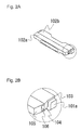
- 400 Light emitting device
- 101, 401, 601 Lead electrodes
- 101 a, 401 a End portions of the lead electrodes
- 102, 402, 602 Package
- 102 a Front side Package
- 102 b Rear side package
- 103, 403 First face
- 104, 404 Second face
- 105, 405 Third face
- 106 Recess
- 307, 308 Molding die
- 309 Hanger lead electrodes
- 410 Draft
- 411 Notch
- 612 Space
- 413 Forth face
Claims (22)
Applications Claiming Priority (4)
| Application Number | Priority Date | Filing Date | Title |
|---|---|---|---|
| JP2007-078521 | 2007-03-26 | ||
| JPP2007-078521 | 2007-03-26 | ||
| JP2007078521 | 2007-03-26 | ||
| PCT/JP2008/055216 WO2008117737A1 (en) | 2007-03-26 | 2008-03-21 | Light emitting device |
Publications (2)
| Publication Number | Publication Date |
|---|---|
| US20100109042A1 US20100109042A1 (en) | 2010-05-06 |
| US8251530B2 true US8251530B2 (en) | 2012-08-28 |
Family
ID=39788472
Family Applications (1)
| Application Number | Title | Priority Date | Filing Date |
|---|---|---|---|
| US12/593,205 Active 2029-01-20 US8251530B2 (en) | 2007-03-26 | 2008-03-21 | Light emitting device |
Country Status (7)
| Country | Link |
|---|---|
| US (1) | US8251530B2 (en) |
| EP (1) | EP2136414B1 (en) |
| JP (1) | JP5233992B2 (en) |
| KR (1) | KR101455431B1 (en) |
| CN (1) | CN101641803B (en) |
| TW (1) | TWI463691B (en) |
| WO (1) | WO2008117737A1 (en) |
Families Citing this family (7)
| Publication number | Priority date | Publication date | Assignee | Title |
|---|---|---|---|---|
| JP2012028699A (en) | 2010-07-27 | 2012-02-09 | Panasonic Corp | Semiconductor device, lead frame assembly and manufacturing method of the same |
| JP6395045B2 (en) | 2014-11-18 | 2018-09-26 | 日亜化学工業株式会社 | Composite substrate, light emitting device, and manufacturing method thereof |
| JP6264366B2 (en) * | 2015-01-30 | 2018-01-24 | 日亜化学工業株式会社 | Carrier tape and packaging |
| CN105870293B (en) | 2015-01-30 | 2019-12-13 | 日亚化学工业株式会社 | Carrier tape and package |
| JP2015159324A (en) * | 2015-04-30 | 2015-09-03 | 大日本印刷株式会社 | Lead frame for led with reflector, and manufacturing method of semiconductor apparatus employing the same |
| KR102486035B1 (en) * | 2016-01-28 | 2023-01-06 | 쑤저우 레킨 세미컨덕터 컴퍼니 리미티드 | Light emitting device package and light emitting apparatus having the same |
| US11081627B2 (en) * | 2018-08-31 | 2021-08-03 | Nichia Corporation | Semiconductor device and method for manufacturing the same |
Citations (12)
| Publication number | Priority date | Publication date | Assignee | Title |
|---|---|---|---|---|
| JPS5967659A (en) | 1982-10-12 | 1984-04-17 | Hitachi Ltd | Semiconductor device |
| JP2002049334A (en) | 1999-11-01 | 2002-02-15 | Rohm Co Ltd | Light emitting display device and producing method thereof |
| JP2002280616A (en) | 2001-03-16 | 2002-09-27 | Nichia Chem Ind Ltd | Package mold and light emitting device using the same |
| JP2003168824A (en) | 2001-11-30 | 2003-06-13 | Sanyo Electric Co Ltd | Led display and its manufacturing method |
| US6603404B1 (en) | 1999-11-01 | 2003-08-05 | Rohm Co., Ltd. | Light emitting display device and method of making the same |
| JP2004207688A (en) | 2002-12-09 | 2004-07-22 | Nichia Chem Ind Ltd | Light emitting device and planar light source using the same |
| US20040240229A1 (en) * | 2001-07-09 | 2004-12-02 | Osram Opto Semiconductors Gmbh | Led module for illumination systems |
| EP1538680A2 (en) | 2003-12-03 | 2005-06-08 | Sumitomo Electric Industries, Ltd. | Light emitting device |
| US20060022216A1 (en) | 2004-08-02 | 2006-02-02 | Sharp Kabushiki Kaisha | Semiconductor light-emitting device and method of manufacturing the same |
| JP2006253551A (en) | 2005-03-14 | 2006-09-21 | Matsushita Electric Ind Co Ltd | Semiconductor light emitting device |
| US20070147087A1 (en) * | 1995-06-27 | 2007-06-28 | Parker Jeffery R | Light emitting panel assemblies |
| US7815339B2 (en) * | 2008-01-09 | 2010-10-19 | Innotec Corporation | Light module |
Family Cites Families (5)
| Publication number | Priority date | Publication date | Assignee | Title |
|---|---|---|---|---|
| JPS61269338A (en) * | 1985-05-24 | 1986-11-28 | Hitachi Ltd | Resin-sealed semiconductor device and molding die used for manufacture thereof |
| JP3708026B2 (en) * | 2001-04-12 | 2005-10-19 | 豊田合成株式会社 | LED lamp |
| TWI292961B (en) * | 2002-09-05 | 2008-01-21 | Nichia Corp | Semiconductor device and an optical device using the semiconductor device |
| JP2005260276A (en) * | 2003-12-03 | 2005-09-22 | Sumitomo Electric Ind Ltd | Light-emitting device |
| TWI247435B (en) * | 2004-03-09 | 2006-01-11 | Opto Tech Corp | Side-emitting LED package structure |
-
2008
- 2008-03-21 CN CN2008800098360A patent/CN101641803B/en active Active
- 2008-03-21 EP EP08722580.1A patent/EP2136414B1/en active Active
- 2008-03-21 KR KR1020097020051A patent/KR101455431B1/en active IP Right Grant
- 2008-03-21 US US12/593,205 patent/US8251530B2/en active Active
- 2008-03-21 JP JP2009506315A patent/JP5233992B2/en active Active
- 2008-03-21 WO PCT/JP2008/055216 patent/WO2008117737A1/en active Application Filing
- 2008-03-26 TW TW097110854A patent/TWI463691B/en active
Patent Citations (13)
| Publication number | Priority date | Publication date | Assignee | Title |
|---|---|---|---|---|
| JPS5967659A (en) | 1982-10-12 | 1984-04-17 | Hitachi Ltd | Semiconductor device |
| US20070147087A1 (en) * | 1995-06-27 | 2007-06-28 | Parker Jeffery R | Light emitting panel assemblies |
| JP2002049334A (en) | 1999-11-01 | 2002-02-15 | Rohm Co Ltd | Light emitting display device and producing method thereof |
| US6603404B1 (en) | 1999-11-01 | 2003-08-05 | Rohm Co., Ltd. | Light emitting display device and method of making the same |
| JP2002280616A (en) | 2001-03-16 | 2002-09-27 | Nichia Chem Ind Ltd | Package mold and light emitting device using the same |
| US20040240229A1 (en) * | 2001-07-09 | 2004-12-02 | Osram Opto Semiconductors Gmbh | Led module for illumination systems |
| JP2003168824A (en) | 2001-11-30 | 2003-06-13 | Sanyo Electric Co Ltd | Led display and its manufacturing method |
| JP2004207688A (en) | 2002-12-09 | 2004-07-22 | Nichia Chem Ind Ltd | Light emitting device and planar light source using the same |
| EP1538680A2 (en) | 2003-12-03 | 2005-06-08 | Sumitomo Electric Industries, Ltd. | Light emitting device |
| US20060022216A1 (en) | 2004-08-02 | 2006-02-02 | Sharp Kabushiki Kaisha | Semiconductor light-emitting device and method of manufacturing the same |
| JP2006049442A (en) | 2004-08-02 | 2006-02-16 | Sharp Corp | Semiconductor light emission device and its manufacturing method |
| JP2006253551A (en) | 2005-03-14 | 2006-09-21 | Matsushita Electric Ind Co Ltd | Semiconductor light emitting device |
| US7815339B2 (en) * | 2008-01-09 | 2010-10-19 | Innotec Corporation | Light module |
Non-Patent Citations (1)
| Title |
|---|
| Extended European Search Report dated Jul. 4, 2011 for Application No. 08722580.1. |
Also Published As
| Publication number | Publication date |
|---|---|
| CN101641803B (en) | 2011-05-18 |
| TW200901516A (en) | 2009-01-01 |
| KR20090127294A (en) | 2009-12-10 |
| EP2136414B1 (en) | 2015-12-23 |
| US20100109042A1 (en) | 2010-05-06 |
| CN101641803A (en) | 2010-02-03 |
| EP2136414A1 (en) | 2009-12-23 |
| JPWO2008117737A1 (en) | 2010-07-15 |
| EP2136414A4 (en) | 2011-08-03 |
| JP5233992B2 (en) | 2013-07-10 |
| WO2008117737A1 (en) | 2008-10-02 |
| TWI463691B (en) | 2014-12-01 |
| KR101455431B1 (en) | 2014-10-27 |
Similar Documents
| Publication | Publication Date | Title |
|---|---|---|
| KR101602977B1 (en) | Light-emitting device | |
| US10153415B2 (en) | Light emitting device having dual sealing resins | |
| JP5119621B2 (en) | Light emitting device | |
| KR100901618B1 (en) | Light emitting diode package and manufacturing method thereof | |
| US7833811B2 (en) | Side-emitting LED package and method of manufacturing the same | |
| KR101635650B1 (en) | Light emitting device | |
| US8251530B2 (en) | Light emitting device | |
| US7527400B2 (en) | Light emitting device | |
| EP3499590B1 (en) | Light emitting device package | |
| US20090315068A1 (en) | Light emitting device | |
| TW201644073A (en) | Light emitting device, resin package, resin compact and method of manufacturing the same | |
| KR20110103929A (en) | Light emitting diode package and light unit having the same | |
| JP5233478B2 (en) | Light emitting device | |
| JP2008160091A (en) | Light-emitting device | |
| JP5722759B2 (en) | Light emitting device |
Legal Events
| Date | Code | Title | Description |
|---|---|---|---|
| AS | Assignment |
Owner name: NICHIA CORPORATION,JAPAN Free format text: ASSIGNMENT OF ASSIGNORS INTEREST;ASSIGNOR:ASAKAWA, HIDEO;REEL/FRAME:023499/0047 Effective date: 20091017 Owner name: NICHIA CORPORATION, JAPAN Free format text: ASSIGNMENT OF ASSIGNORS INTEREST;ASSIGNOR:ASAKAWA, HIDEO;REEL/FRAME:023499/0047 Effective date: 20091017 |
|
| STCF | Information on status: patent grant |
Free format text: PATENTED CASE |
|
| FEPP | Fee payment procedure |
Free format text: PAYOR NUMBER ASSIGNED (ORIGINAL EVENT CODE: ASPN); ENTITY STATUS OF PATENT OWNER: LARGE ENTITY |
|
| FPAY | Fee payment |
Year of fee payment: 4 |
|
| MAFP | Maintenance fee payment |
Free format text: PAYMENT OF MAINTENANCE FEE, 8TH YEAR, LARGE ENTITY (ORIGINAL EVENT CODE: M1552); ENTITY STATUS OF PATENT OWNER: LARGE ENTITY Year of fee payment: 8 |
|
| MAFP | Maintenance fee payment |
Free format text: PAYMENT OF MAINTENANCE FEE, 12TH YEAR, LARGE ENTITY (ORIGINAL EVENT CODE: M1553); ENTITY STATUS OF PATENT OWNER: LARGE ENTITY Year of fee payment: 12 |