EP1535190B1 - Method of operating simultaneously a sequential processor and a reconfigurable array - Google Patents
Method of operating simultaneously a sequential processor and a reconfigurable array Download PDFInfo
- Publication number
- EP1535190B1 EP1535190B1 EP03784053A EP03784053A EP1535190B1 EP 1535190 B1 EP1535190 B1 EP 1535190B1 EP 03784053 A EP03784053 A EP 03784053A EP 03784053 A EP03784053 A EP 03784053A EP 1535190 B1 EP1535190 B1 EP 1535190B1
- Authority
- EP
- European Patent Office
- Prior art keywords
- loop
- data
- iram
- xpp
- memory
- Prior art date
- Legal status (The legal status is an assumption and is not a legal conclusion. Google has not performed a legal analysis and makes no representation as to the accuracy of the status listed.)
- Expired - Lifetime
Links
- 238000000034 method Methods 0.000 title claims abstract description 88
- 230000015654 memory Effects 0.000 claims description 211
- 239000013598 vector Substances 0.000 claims description 91
- 230000036316 preload Effects 0.000 claims description 77
- 238000013507 mapping Methods 0.000 claims description 17
- 230000000903 blocking effect Effects 0.000 claims description 4
- 238000012545 processing Methods 0.000 description 144
- 230000006870 function Effects 0.000 description 136
- 238000005457 optimization Methods 0.000 description 114
- 230000009466 transformation Effects 0.000 description 91
- 238000004458 analytical method Methods 0.000 description 67
- 238000004422 calculation algorithm Methods 0.000 description 43
- 238000000844 transformation Methods 0.000 description 40
- 230000014509 gene expression Effects 0.000 description 28
- 238000003491 array Methods 0.000 description 26
- 230000000694 effects Effects 0.000 description 26
- 238000004891 communication Methods 0.000 description 24
- 239000011800 void material Substances 0.000 description 24
- 238000004364 calculation method Methods 0.000 description 23
- 230000008569 process Effects 0.000 description 23
- 238000010168 coupling process Methods 0.000 description 22
- 238000009826 distribution Methods 0.000 description 22
- 238000005859 coupling reaction Methods 0.000 description 20
- 230000009467 reduction Effects 0.000 description 20
- 238000012546 transfer Methods 0.000 description 20
- 230000008878 coupling Effects 0.000 description 19
- 230000015572 biosynthetic process Effects 0.000 description 18
- 238000000638 solvent extraction Methods 0.000 description 18
- 238000003786 synthesis reaction Methods 0.000 description 18
- 238000011068 loading method Methods 0.000 description 17
- 238000013461 design Methods 0.000 description 16
- 230000004927 fusion Effects 0.000 description 16
- 238000007726 management method Methods 0.000 description 16
- 230000008901 benefit Effects 0.000 description 15
- 230000008030 elimination Effects 0.000 description 15
- 238000003379 elimination reaction Methods 0.000 description 15
- 238000005065 mining Methods 0.000 description 15
- 230000008859 change Effects 0.000 description 13
- 238000010606 normalization Methods 0.000 description 13
- 230000036961 partial effect Effects 0.000 description 13
- 230000001965 increasing effect Effects 0.000 description 12
- 230000006698 induction Effects 0.000 description 11
- 238000013139 quantization Methods 0.000 description 11
- 101150065184 sym-2 gene Proteins 0.000 description 11
- 238000000926 separation method Methods 0.000 description 10
- 230000003068 static effect Effects 0.000 description 10
- 238000005516 engineering process Methods 0.000 description 9
- 101150004636 SYM1 gene Proteins 0.000 description 8
- XUIMIQQOPSSXEZ-UHFFFAOYSA-N Silicon Chemical compound [Si] XUIMIQQOPSSXEZ-UHFFFAOYSA-N 0.000 description 8
- 230000001934 delay Effects 0.000 description 8
- 230000006872 improvement Effects 0.000 description 8
- 230000033001 locomotion Effects 0.000 description 8
- 229910052710 silicon Inorganic materials 0.000 description 8
- 239000010703 silicon Substances 0.000 description 8
- 230000001360 synchronised effect Effects 0.000 description 8
- 230000002123 temporal effect Effects 0.000 description 8
- 238000013459 approach Methods 0.000 description 7
- 238000006243 chemical reaction Methods 0.000 description 7
- 238000011161 development Methods 0.000 description 7
- 230000007246 mechanism Effects 0.000 description 7
- 101100366946 Arabidopsis thaliana STOP1 gene Proteins 0.000 description 6
- 230000000670 limiting effect Effects 0.000 description 6
- 239000011159 matrix material Substances 0.000 description 6
- 238000002360 preparation method Methods 0.000 description 6
- 230000002829 reductive effect Effects 0.000 description 6
- 238000012360 testing method Methods 0.000 description 6
- 230000003111 delayed effect Effects 0.000 description 5
- 230000002708 enhancing effect Effects 0.000 description 5
- 230000010354 integration Effects 0.000 description 5
- 230000004044 response Effects 0.000 description 5
- 230000002441 reversible effect Effects 0.000 description 5
- 238000006467 substitution reaction Methods 0.000 description 5
- 230000009286 beneficial effect Effects 0.000 description 4
- 239000012141 concentrate Substances 0.000 description 4
- 230000001419 dependent effect Effects 0.000 description 4
- 230000004048 modification Effects 0.000 description 4
- 238000012986 modification Methods 0.000 description 4
- 238000003860 storage Methods 0.000 description 4
- 230000001960 triggered effect Effects 0.000 description 4
- 230000006399 behavior Effects 0.000 description 3
- 230000008602 contraction Effects 0.000 description 3
- 238000007667 floating Methods 0.000 description 3
- 238000005206 flow analysis Methods 0.000 description 3
- 230000008520 organization Effects 0.000 description 3
- 230000002411 adverse Effects 0.000 description 2
- 238000010276 construction Methods 0.000 description 2
- 230000009977 dual effect Effects 0.000 description 2
- 238000005265 energy consumption Methods 0.000 description 2
- 238000011156 evaluation Methods 0.000 description 2
- 238000011049 filling Methods 0.000 description 2
- 238000001914 filtration Methods 0.000 description 2
- 238000011010 flushing procedure Methods 0.000 description 2
- 238000010295 mobile communication Methods 0.000 description 2
- 230000008521 reorganization Effects 0.000 description 2
- 238000004088 simulation Methods 0.000 description 2
- 230000007704 transition Effects 0.000 description 2
- 238000013519 translation Methods 0.000 description 2
- LHMQDVIHBXWNII-UHFFFAOYSA-N 3-amino-4-methoxy-n-phenylbenzamide Chemical compound C1=C(N)C(OC)=CC=C1C(=O)NC1=CC=CC=C1 LHMQDVIHBXWNII-UHFFFAOYSA-N 0.000 description 1
- 241000272165 Charadriidae Species 0.000 description 1
- RYGMFSIKBFXOCR-UHFFFAOYSA-N Copper Chemical compound [Cu] RYGMFSIKBFXOCR-UHFFFAOYSA-N 0.000 description 1
- 238000012893 Hill function Methods 0.000 description 1
- 101000969688 Homo sapiens Macrophage-expressed gene 1 protein Proteins 0.000 description 1
- 102100021285 Macrophage-expressed gene 1 protein Human genes 0.000 description 1
- 241000761456 Nops Species 0.000 description 1
- 230000003213 activating effect Effects 0.000 description 1
- 230000004913 activation Effects 0.000 description 1
- 230000006978 adaptation Effects 0.000 description 1
- 230000003044 adaptive effect Effects 0.000 description 1
- 229910052782 aluminium Inorganic materials 0.000 description 1
- 239000004411 aluminium Substances 0.000 description 1
- XAGFODPZIPBFFR-UHFFFAOYSA-N aluminium Chemical compound [Al] XAGFODPZIPBFFR-UHFFFAOYSA-N 0.000 description 1
- 230000004888 barrier function Effects 0.000 description 1
- 230000015556 catabolic process Effects 0.000 description 1
- 239000002131 composite material Substances 0.000 description 1
- 150000001875 compounds Chemical class 0.000 description 1
- 230000006835 compression Effects 0.000 description 1
- 238000007906 compression Methods 0.000 description 1
- 238000004590 computer program Methods 0.000 description 1
- 230000003750 conditioning effect Effects 0.000 description 1
- 229910052802 copper Inorganic materials 0.000 description 1
- 239000010949 copper Substances 0.000 description 1
- 230000001186 cumulative effect Effects 0.000 description 1
- 125000004122 cyclic group Chemical group 0.000 description 1
- 230000006837 decompression Effects 0.000 description 1
- 230000003247 decreasing effect Effects 0.000 description 1
- 238000006731 degradation reaction Methods 0.000 description 1
- 238000010586 diagram Methods 0.000 description 1
- 230000003467 diminishing effect Effects 0.000 description 1
- 238000006073 displacement reaction Methods 0.000 description 1
- 230000004992 fission Effects 0.000 description 1
- 229910052738 indium Inorganic materials 0.000 description 1
- 230000003993 interaction Effects 0.000 description 1
- 238000005304 joining Methods 0.000 description 1
- 239000000203 mixture Substances 0.000 description 1
- 230000001343 mnemonic effect Effects 0.000 description 1
- 108010020615 nociceptin receptor Proteins 0.000 description 1
- 238000010397 one-hybrid screening Methods 0.000 description 1
- 238000005192 partition Methods 0.000 description 1
- 230000002093 peripheral effect Effects 0.000 description 1
- 238000007781 pre-processing Methods 0.000 description 1
- 230000008707 rearrangement Effects 0.000 description 1
- 230000003252 repetitive effect Effects 0.000 description 1
- 230000003362 replicative effect Effects 0.000 description 1
- 238000011160 research Methods 0.000 description 1
- 230000000717 retained effect Effects 0.000 description 1
- 239000004065 semiconductor Substances 0.000 description 1
- 230000008054 signal transmission Effects 0.000 description 1
- 239000007787 solid Substances 0.000 description 1
- 230000005236 sound signal Effects 0.000 description 1
- 230000007480 spreading Effects 0.000 description 1
- 238000003892 spreading Methods 0.000 description 1
- 239000002699 waste material Substances 0.000 description 1
Images


Classifications
-
- G—PHYSICS
- G06—COMPUTING; CALCULATING OR COUNTING
- G06F—ELECTRIC DIGITAL DATA PROCESSING
- G06F9/00—Arrangements for program control, e.g. control units
- G06F9/06—Arrangements for program control, e.g. control units using stored programs, i.e. using an internal store of processing equipment to receive or retain programs
- G06F9/30—Arrangements for executing machine instructions, e.g. instruction decode
- G06F9/30181—Instruction operation extension or modification
-
- G—PHYSICS
- G06—COMPUTING; CALCULATING OR COUNTING
- G06F—ELECTRIC DIGITAL DATA PROCESSING
- G06F15/00—Digital computers in general; Data processing equipment in general
- G06F15/76—Architectures of general purpose stored program computers
- G06F15/78—Architectures of general purpose stored program computers comprising a single central processing unit
- G06F15/7867—Architectures of general purpose stored program computers comprising a single central processing unit with reconfigurable architecture
-
- G—PHYSICS
- G06—COMPUTING; CALCULATING OR COUNTING
- G06F—ELECTRIC DIGITAL DATA PROCESSING
- G06F9/00—Arrangements for program control, e.g. control units
- G06F9/06—Arrangements for program control, e.g. control units using stored programs, i.e. using an internal store of processing equipment to receive or retain programs
- G06F9/30—Arrangements for executing machine instructions, e.g. instruction decode
- G06F9/34—Addressing or accessing the instruction operand or the result ; Formation of operand address; Addressing modes
- G06F9/345—Addressing or accessing the instruction operand or the result ; Formation of operand address; Addressing modes of multiple operands or results
- G06F9/3455—Addressing or accessing the instruction operand or the result ; Formation of operand address; Addressing modes of multiple operands or results using stride
-
- G—PHYSICS
- G06—COMPUTING; CALCULATING OR COUNTING
- G06F—ELECTRIC DIGITAL DATA PROCESSING
- G06F9/00—Arrangements for program control, e.g. control units
- G06F9/06—Arrangements for program control, e.g. control units using stored programs, i.e. using an internal store of processing equipment to receive or retain programs
- G06F9/30—Arrangements for executing machine instructions, e.g. instruction decode
- G06F9/38—Concurrent instruction execution, e.g. pipeline, look ahead
- G06F9/3802—Instruction prefetching
-
- G—PHYSICS
- G06—COMPUTING; CALCULATING OR COUNTING
- G06F—ELECTRIC DIGITAL DATA PROCESSING
- G06F9/00—Arrangements for program control, e.g. control units
- G06F9/06—Arrangements for program control, e.g. control units using stored programs, i.e. using an internal store of processing equipment to receive or retain programs
- G06F9/30—Arrangements for executing machine instructions, e.g. instruction decode
- G06F9/38—Concurrent instruction execution, e.g. pipeline, look ahead
- G06F9/3824—Operand accessing
- G06F9/383—Operand prefetching
-
- G—PHYSICS
- G06—COMPUTING; CALCULATING OR COUNTING
- G06F—ELECTRIC DIGITAL DATA PROCESSING
- G06F9/00—Arrangements for program control, e.g. control units
- G06F9/06—Arrangements for program control, e.g. control units using stored programs, i.e. using an internal store of processing equipment to receive or retain programs
- G06F9/30—Arrangements for executing machine instructions, e.g. instruction decode
- G06F9/38—Concurrent instruction execution, e.g. pipeline, look ahead
- G06F9/3836—Instruction issuing, e.g. dynamic instruction scheduling or out of order instruction execution
- G06F9/3851—Instruction issuing, e.g. dynamic instruction scheduling or out of order instruction execution from multiple instruction streams, e.g. multistreaming
-
- G—PHYSICS
- G06—COMPUTING; CALCULATING OR COUNTING
- G06F—ELECTRIC DIGITAL DATA PROCESSING
- G06F9/00—Arrangements for program control, e.g. control units
- G06F9/06—Arrangements for program control, e.g. control units using stored programs, i.e. using an internal store of processing equipment to receive or retain programs
- G06F9/30—Arrangements for executing machine instructions, e.g. instruction decode
- G06F9/38—Concurrent instruction execution, e.g. pipeline, look ahead
- G06F9/3877—Concurrent instruction execution, e.g. pipeline, look ahead using a slave processor, e.g. coprocessor
-
- G—PHYSICS
- G06—COMPUTING; CALCULATING OR COUNTING
- G06F—ELECTRIC DIGITAL DATA PROCESSING
- G06F9/00—Arrangements for program control, e.g. control units
- G06F9/06—Arrangements for program control, e.g. control units using stored programs, i.e. using an internal store of processing equipment to receive or retain programs
- G06F9/30—Arrangements for executing machine instructions, e.g. instruction decode
- G06F9/38—Concurrent instruction execution, e.g. pipeline, look ahead
- G06F9/3885—Concurrent instruction execution, e.g. pipeline, look ahead using a plurality of independent parallel functional units
- G06F9/3893—Concurrent instruction execution, e.g. pipeline, look ahead using a plurality of independent parallel functional units controlled in tandem, e.g. multiplier-accumulator
- G06F9/3895—Concurrent instruction execution, e.g. pipeline, look ahead using a plurality of independent parallel functional units controlled in tandem, e.g. multiplier-accumulator for complex operations, e.g. multidimensional or interleaved address generators, macros
- G06F9/3897—Concurrent instruction execution, e.g. pipeline, look ahead using a plurality of independent parallel functional units controlled in tandem, e.g. multiplier-accumulator for complex operations, e.g. multidimensional or interleaved address generators, macros with adaptable data path
Definitions
- the present invention relates to methods of operating reconfigurable arrays of data processing elements.
- a PLD instruction can be used to tell the memory system that an access to the data at a specified memory address is likely to occur soon. A memory system that recognizes this request will bring the data into cache so that when the access actually occurs any delay caused by a cache miss is reduced or eliminated.
- an integrated digital signal processor that uses an architecture which includes both a general purpose processor and a vector processor.
- the integrated digital signal processor also includes a cache subsystem, a first bus and a second bus.
- the cache subsystem provides caching and data routing for the processors and buses. Multiple simultaneous communication paths can be used in the cache subsystem for the processors and buses. Furthermore, simultaneous reads and writes are supported to a cache memory in the known cache subsystem.
- a method of operating a computer system comprising at least one microprocessor (MP) and coprocessors (COP), in which the coprocessor (COP) is made up of a plurality of functional units (F(i)), each of which is specialized for the execution of a function, in which, for a user program to be processed, the command sequences which can be executed by a coprocessor are established during the compiling of said program, and in which, according to the established command sequence, one of the functional units of the coprocessor is selected and connected to the microprocessor (MP).
- MP microprocessor
- COP coprocessors
- Garp Architecture A further document relating to the Garp Architecture is J. Hauser et al. "Garp: A MIPS processor with a Reconfigurable coprocessor", ISSN 0-8186-8159-4/97 .
- a reconfigurable multifunction computing cache architecture is known from H. Kim et al, IEEE Transactions on very large scale Integration (VLSI) Systems, Vol. 9, No.4, August 2001 .
- the present invention aims at providing improvements over the prior art.
- the proposed hardware framework accelerates the XPP core in two respects.
- data throughput is increased by raising the XPP's internal operating frequency into the range of the RISC's frequency. This, however, means that the XPP runs into the same pit like all high frequency processors - memory accesses become very slow compared to processor internal computations. This is why the use of a cache is proposed. It eases the memory access problem for a large range of algorithms, which are well suited for an execution on the XPP.
- the cache as second throughput increasing feature requires a controller. Hence a programmable cache controller is introduced, which manages the cache contents and feeds the XPP core. It decouples the XPP core computations from the data transfer so that, for instance, data preload to a specific cache sector takes place while the XPP is operating on data located in a different cache sector.
- the proposed cache concept is based on a simple IRAM cell structure allowing for an easy scalability of the hardware - extending the XPP cache size, for instance, requires not much more than the duplication of IRAM cells.
- the objective of the compiler is that real-world applications, which are written in the C language, can be compiled for a RISC+XPP system.
- the compiler removes the necessity of developing NML code for the XPP by hand. It is possible, instead, to implement algorithms in the C language or to directly use existing C applications without much adaptation to the XPP system.
- the proposed compiler includes three major components to perform the compilation process for the XPP:
- the partitioning component of the compiler decides which parts of an application code can be executed on the XPP and which parts are executed on the RISC.
- Typical candidates for becoming XPP code are loops with a large number of iterations whose loop bodies are dominated by arithmetic operations.
- the remaining source code - including the data transfer code - is compiled for the RISC.
- the proposed compiler transforms the XPP code such that it is optimized for NML code generation.
- the transformations included in the compiler comprise a large number of loop transformations as well as general code transformations.
- the compiler restructures the code so that it fits into the XPP array and that the final performance exceeds the pure RISC performance.
- the compiler generates NML code from the transformed program.
- the whole compilation process is controlled by an optimization driver which selects the optimal order of transformations based on the source code.
- RISC instructions of totally different type (Ld/St, ALU, Mul/Div/MAC, FPALU, FPMul...) are executed in separate specialized functional units to increase the fraction of silicon that is busy on average.
- Such functional unit separation has led to superscalar RISC designs, that exploit higher levels of parallelism.
- Each functional unit of a RISC core is highly pipelined to improve throughput Pipelining overlaps the execution of several instructions by splitting them into unrelated phases, which are executed in different stages of the pipeline. Thus different stages of consecutive instructions can be executed in parallel with each stage taking much less time to execute. This allows higher core frequencies.
- SMT simultaneous multithreading
- the multi cycle execution time also forbids a strongly synchronous execution scheme and rather leads to an asynchronous scheme, like for e.g. floating point square root units. This in turn necessitates the existence of explicit synchronization instructions.
- the XPP's operating frequency will either be half of the core frequency or equal to the core frequency of the RISC.
- This memory hierarchy does not help to speed up computations which shuffle large amounts of data, with little or no data reuse. These computations are called “bounded by memory bandwidth”. However other types of computations with more data locality (another name for data reuse) gain performance as long as they fit into one of the upper layers of the memory hierarchy. This is the class of applications that gain the highest speedups when a memory hierarchy is introduced.
- Classical vectorization can be used to transform memory-bounded algorithms, with a data set too big to fit into the upper layers of the memory hierarchy. Rewriting the code to reuse smaller data sets sooner exposes memory reuse on a smaller scale. As the new data set size is chosen to fit into the caches of the memory hierarchy, the algorithm is not memory bounded any more, yielding significant speed-ups.
- the changed environment - higher frequency and the memory hierarchy - not only necessitate reconsideration of hardware design parameters, but also a reevaluation of the software environment.
- Modem microprocessors gain their performance from multiple specialized and deeply pipelined functional units and high memory hierarchies, enabling high core frequencies. But high memory hierarchies mean that there is a high penalty for cache misses due to the difference between core and memory frequency. Many core cycles pass until the values are finally available from memory. Deep pipelines incur pipeline stalls due to data dependencies as well as branch penalties for mispredicted conditional branches. Specialized functional units like floating point units idle for integer-only programs. For these reasons, average functional unit utilization is much too low.
- SMT Simultaneous MultiThreading
- SMT the task (process) switching is done in hardware, so the processor state has to be duplicated in hardware. So again it is most efficient to keep the state as small as possible.
- SMT is very beneficial, since the XPP configurations execute longer than the average RISC instruction.
- another task can utilize the other functional units, while a configuration is running.
- not every task will utilize the XPP, so while one such non-XPP task is running, another one will be able to use the XPP core.
- streaming can only support (number_of_IO_ports * width_of_IO_port) bits per cycle, it is only well suited for small XPP arrays with heavily pipelined configurations that feature few inputs and outputs. As the pipelines take a long time to fill and empty while the running time of a configuration is limited (as described under "context switches"), this type of communication does not scale well to bigger XPP arrays and XPP frequencies near the RISC core frequency.
- the RISC supplies the XPP array with the streaming data. Since the RISC core has to execute several instructions to compute addresses and load an item from memory, this setup is only suited, if the XPP core is reading data with a frequency much lower than the RISC core frequency.
- the RISC core only initializes a DMA channel which then supplies the data items to the streaming port of the XPP core.
- the XPP array configuration uses a number of PAEs to generate an address that is used to access main memory through the IO ports.
- this approach suffers from the same limitations as the previous one, although for larger XPP arrays there is less impact of using PAEs for address generation.
- this approach is still useful for loading values from very sparse vectors.
- This data access mechanism uses the IRAM elements to store data for local computations.
- the IRAMs can either be viewed as vector registers or as local copies of main memory.
- the size of the state is crucial for the efficiency of context switches.
- the size of the state is fixed for the XPP core, it depends on the declaration of the various state elements, whether they have to be saved or not.
- the state of the XPP core can be classified as
- a configuration is defined to be uninterruptible (non pre-emptive)
- all of the local state on the busses and in the PAEs can be declared as scratch. This means that every configuration gets its input data from the IRAMs and writes its output data to the IRAMs. So after the configuration has finished all information in the PAEs and on the buses is redundant or invalid and does not have to be saved.
- the configuration manager handles manual preloading of configurations. Preloading will help in parallelizing the memory transfers with other computations during the task switch. This cache can also reduce the memory traffic for frequent context switches, provided that a Least Recently Used (LRU) replacement strategy is implemented in addition to the preload mechanism.
- LRU Least Recently Used
- the IRAMs can be defined to be local cache copies of main memory as proposed as fourth method in section 2.2.3. Then each IRAM is associated with a starting address and modification state information. The IRAM memory cells are replicated.
- An IRAM PEA contains an IRAM block with multiple IRAM instances. Only the starting addresses of the IRAMs have to be saved and restored as context. The starting addresses for the IRAMs of the current configuration select the IRAM instances with identical addresses to be used.
- IRAM instance If no empty IRAM instance is available, a clean (unmodified) instance is declared empty (and hence must be reloaded later on).
- This delay can be avoided, if a separate state machine (cache controller) tries to clean inactive IRAM instances by using unused memory cycles to write back the IRAM instances' contents.
- processors are viewed as executing a single stream of instructions. But today's multi tasking operating systems support hundreds of tasks being executed on a single processor. This is achieved by switching contexts, where all, or at least the most relevant parts of the processor state, which belong to the current task - the task's context - is exchanged with the state of another task, that will be executed next.
- SMT simultaneous multi-threading
- ISR Interrupt Service Routine
- This type of context switch is executed without software interaction, totally in hardware. Instructions of several instruction streams are merged into a single instruction stream to increase instruction level parallelism and improve functional unit utilization. Hence the processor state cannot be stored to and reloaded from memory between instructions from different instruction streams: Imagine the worst case of alternating instructions from two streams and the hundreds to thousand of cycles needed to write the processor state to memory and read in another state.
- the size of the state also increases the silicon area needed to implement SMT, so the size of the state is crucial for many design decisions.
- the part of the state, which is destroyed by the jump to the ISR, is saved by hardware (e.g. the program counter). It is the ISR's responsibility to save and restore the state of all other resources, that are actually used within the ISR.
- the execution model of the instructions will also affect the tradeoff between short interrupt latencies and maximum throughput: Throughput is maximized if the instructions in the pipeline are finished, and the instructions of the ISR are chained. This adversely affects the interrupt latency. If, however, the instructions are abandoned (pre-empted) in favor of a short interrupt latency, they must be fetched again later, which affects throughput. The third possibility would be to save the internal state of the instructions within the pipeline, but this requires too much hardware effort. Usually this is not done.
- This type of context switch is executed totally in software. All of a task's context (state) has to be saved to memory, and the context of the new task has to be reloaded. Since tasks are usually allowed to use all of the processor's resources to achieve top performance, all of the processor state has to be saved and restored. If the amount of state is excessive, the rate of context switches must be decreased by less frequent rescheduling, or a severe throughput degradation will result, as most of the time will be spent in saving and restoring task contexts. This in turn increases the response time for the tasks.
- IRAM content is an explicitly preloaded memory area, a virtually unlimited number of such IRAMs can be used. They are identified by their memory address and their size. The IRAM content is explicitly preloaded by the application. Caching will increase performance by reusing data from the memory hierarchy. The cached operation also eliminates the need for explicit store instructions; they are handled implicitly by cache write back operations but can also be forced to synchronize with the RISC.
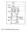
- the pipeline stages of the XPP functional unit are Load, Execute and Write Back (Store).
- the store is executed delayed as a cache write back.
- the pipeline stages execute in an asynchronous fashion, thus hiding the variable delays from the cache preloads and the PAE array.
- the XPP functional unit is decoupled of the RISC by a FIFO, which is fed with the XPP instructions.
- the XPP PAE consumes and executes the configurations and the preloaded IRAMs. Synchronization of the XPP and the RISC is done explicitly by a synchronization instruction.
- the configuration is added to the preload FIFO to be loaded into the configuration cache within the PAE array.
- the parameter is a pointer register of the RISC pointer register file.
- the size is implicitly contained in the configuration.
- This instruction specifies the contents of the IRAM for the next configuration execution. In fact, the memory area is added to the preload FIFO to be loaded into the specified IRAM.
- the first parameter is the IRAM number. This is an immediate (constant) value.
- the second parameter is a pointer to the starting address. This parameter is provided in a pointer register of the RISC pointer register file.
- the third parameter is the size in units of 32 bit words. This is an integer value. It resides in a general-purpose register of the RISC's integer register file.
- the first variant actually preloads the data from memory.
- the second variant is for write-only accesses. It skips the loading operation. Thus no cache misses can occur for this IRAM. Only the address and size are defined. They are obviously needed for the write back operation of the IRAM cache.
- This instruction executes the last preloaded configuration with the last preloaded IRAM contents. Actually a configuration start command is issued to the FIFO. Then the FIFO is advanced; this means that further preload commands will specify the next configuration or parameters for the next configuration. Whenever a configuration finishes, the next one is consumed from the head of the FIFO, if its start command has already been issued.
- This instruction forces write back operations for all IRAMs that overlap the given memory area. If overlapping IRAMs are still in use by a configuration or preloaded to be used, this operation will block. Giving an address of NULL (zero) and a size of MAX_INT (bigger than the actual memory), this instruction can also be used to wait until all issued configurations finish.
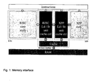
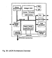
- the XPP core shares the memory hierarchy with the RISC core using a special cache controller.
- the preload-FIFOs in the above figure contain the addresses and sizes for already issued IRAM preloads, exposing them to the XPP cache controller.
- the FIFOs have to be duplicated for every virtual processor in an SMT environment.
- Tag is the typical tag for a cache line containing starting address, size and state ( empty / clean / dirty / in-use ).
- the additional in-use state signals usage by the current configuration.
- the cache controller cannot manipulate these IRAM instances.
- the execute configuration command advances all preload FIFOs, copying the old state to the newly created entry. This way the following preloads replace the previously used IRAMs and configurations. If no preload is issued for an IRAM before the configuration is executed, the preload of the previous configuration is retained. Therefore it is not necessary to repeat identical preloads for an IRAM in consecutive configurations.
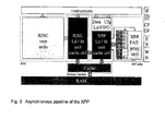
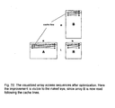
- Fig. 3 The reader should now regard Fig. 3
- Each configuration's execute command has to be delayed (stalled) until all necessary preloads are finished, either explicitly by the use of a synchronization command or implicitly by the cache controller.
- the cache controller (XPP Ld/St unit) has to handle the synchronization and execute commands as well, actually starting the configuration as soon as all data is ready.
- dirty IRAMs are written back to memory as soon as possible, if their content is not reused in the same IRAM.
- the XPP PAE array and the XPP cache controller can be seen as a single unit since they do not have different instruction streams: rather, the cache controller can be seen as the configuration fetch (CF), operand fetch (OF) (IRAM preload) and write back (WB) stage of the XPP pipeline, also triggering the execute stage (EX) (PAE array).
- CF configuration fetch
- OF operand fetch
- WB write back stage
- the reasonable length of the preload FIFO can be several configurations; it is limited by diminishing returns, algorithm properties, the compiler's ability to schedule preloads early and by silicon usage due to the IRAM duplication factor, which has to be at least as big as the FIFO length.
- the interlocking - to avoid data hazards between IRAMs - cannot be done optimally by software (scheduling), but has to be enforced by hardware (hardware interlocking).
- the XPP cache controller and the XPP PAE array can be seen as separate but not totally independent functional units.
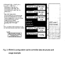
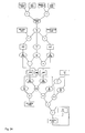
- the XPP cache controller has several tasks. These are depicted as states in the above diagram. State transitions take place along the edges between states, whenever the condition for the edge is true. As soon as the condition is not true any more, the reverse state transition takes place.
- the activities for the states are as follows:
- the XPP cache controller has to fulfill already issued preload commands, while writing back dirty IRAMs as soon as possible.
- a preload in turn can be blocked by an overlapping in-use or dirty IRAM instance in a different block or by the lack of empty IRAM instances in the target IRAM block.
- the former can be resolved by waiting for the configuration to finish and / or by a write back. To resolve the latter, the least recently used clean IRAM can be discarded, thus becoming empty. If no empty or clean IRAM instance exists, a dirty one has to be written back to the memory hierarchy. It cannot occur that no empty, clean or dirty IRAM instances exist, since only one instance can be in-use and there should be more than one instance in an IRAM block - otherwise no is achieved.
- the load FIFOs have to be replicated for every virtual processor.
- the pipelines of the functional units are fed from the shared fetch / reorder / issue stage. All functional units execute in parallel. Different units can execute instructions of different virtual processors.
- IRAM length 128 words
- IRAM duplication factor (pipeline stages+caching factor)*virtual processors: 3 Pipeline stages is the number of pipeline stages LD/EX/WB plus one for every FIFO stage above one: 3 Caching factor is the number of IRAM duplicates available for caching: 0 Virtual processors is the number of virtual processors with SMT: 1
- the size of the state of a virtual processor is mainly dependent on the FIFO length. It is: FIFO length * #IRAM ports * 32 bit Address + 32 bit Size
- the total size of memory used for the IRAMs is: #IRAM ports * IRAM duplication factor * IRAM length * 32 bit
- a first implementation will probably keep close to the above-stated minimum parameters, using a FIFO length of one, an IRAM duplication factor of four, an IRAM length of 128 and no simultaneous multithreading.
- a simple write pointer may be used per IRAM, which keeps track of the last address already in the IRAM. Thus no stall is required, unless an access beyond this write pointer is encountered. This is especially useful, if all IRAMs have to be reloaded after a task switch: The delay to the configuration start can be much shorter, especially, if the preload engine of the cache controller chooses the blocking IRAM next whenever several IRAMs need further loading.
- the frequency at the bottom of the memory hierarchy cannot be raised to the same extent as the frequency of the CPU core.
- the prefetch FIFOs in the above drawing can be extended.
- the IRAM contents for several configurations can be preloaded, like the configurations themselves.
- a simple convention makes clear which IRAM preloads belong to which configuration: the configuration execute switches to the next configuration context. This can be accomplished by advancing the FIFO write pointer with every configuration execute, while leaving it unchanged after every preload. Unassigned IRAM FIFO entries keep their contents from the previous configuration, so every succeeding configuration will use the preceding configuration's IRAMx if no different IRAMx was preloaded.
- a drawback of extending the FIFO length is the increased likelihood that the IRAM content written by an earlier configuration is reused by a later one in another IRAM.
- a cache coherence protocol can clear the situation. Note however that the situation can be resolved more easily: If an overlap between any new IRAM area and a currently dirty IRAM contents of another IRAM bank is detected, the new IRAM is simply not loaded until the write back of the changed IRAM has finished. Thus the execution of the new configuration is delayed until the correct data is available.
- an XPP pipeline stall occurs: The preload can only be started, when the configuration has finished, and - if the content was modified - the memory content has been written to the cache. To decrease the number of pipeline stalls, it is beneficial to add an additional read-only IRAM state. If the IRAM is read only, the content cannot be changed, and the preload of the data to the other IRAM can proceed without delay. This requires an extension to the preload instructions: The XppPreload and the XppPreloadClean instruction formats can be combined to a single instruction format, that has two additional bits, stating whether the IRAM will be read and/or written. To support debugging, violations should be checked at the IRAM ports, raising an exception when needed
- the IRAMs are block-oriented structures, which can be read in any order by the PAE array.
- the address generation adds complexity, reducing the number of PAEs available for the actual computation. So it is best, if the IRAMs are accessed in linear order.
- the memory hierarchy is block oriented as well, further encouraging linear access patterns in the code to avoid cache misses.
- IRAM read ports limit the bandwidth between each IRAM and the PAE array to one word read per cycle, it can be beneficial to distribute the data over several IRAMs to remove this bottleneck.
- the top of the memory hierarchy is the source of the data, so the amount of cache misses never increases when the access pattern is changed, as long as the data locality is not destroyed.
- IRAM Data is duplicated in several IRAMs. This circumvents the IRAM read port bottleneck, allowing several data items to be read from the input every cycle.
- cache misses occur only for the first preload. All other preloads will take place without cache misses - only the time to transfer the data from the top of the memory hierarchy to the IRAMs is needed for every additional load. This is only beneficial, if the cache misses plus the additional transfer times do not exceed the execution time for the configuration.
- the interface of this instruction looks like:
- This instruction behaves as the XPPPreload / XPPPreloadClean instructions with the exception of the first parameter:
- the first parameter is IRAMS. This is an immediate (constant) value.
- the value is a bitmap - for every bit in the bitmap, the IRAM with that number is a target for the load operation.
- Data reordering changes the access pattern to the data only. It does not change the amount of memory that is read. Thus the number of cache misses stays the same.
- a stride (displacement between two elements in memory) is used in vector load operations to load e.g.: a column of a matrix into a vector register.
- One problem with this instruction is that the number of possible cache misses per IRAM load rises: In the worst case it can be one cache miss per loaded value, if the stride is equal to the cache line size and all data is not in the cache. But as already stated: the total number of misses stays the same - just the distribution changes. Still this is an undesirable effect.
- the other problem is the complexity of the implementation and a possibly limited throughput, as the data paths between the layers of the memory hierarchy are optimized for block transfers. Transferring non-contiguous words will not use wide busses in an optimal fashion.
- the interface of the instruction looks like: XPPPreloadStride (int IRAM, void *StartAddress, int Size, int Stride) XPPPreloadCleanStride (int IRAM, void *StartAddress, int Size, int Stride)
- This instruction behaves as the XPPPreload / XPPPreloadClean instructions with the addition of another parameter:
- the fourth parameter is the vector stride. This is an immediate (constant) value. It tells the cache controller, to load only every n th value to the specified IRAM.
- the RISC can copy data at a maximum rate of one word per cycle for simple address computations and at a somewhat lower rate for more complex ones.
- the PAE array can read and write one value from every IRAM per cycle. Thus if half of the IRAMs are used as inputs and half of the IRAMs are used as outputs, up to eight (or more, depending on the number of IRAMs) values can be reordered per cycle, using the PAE array for address generation. As the inputs and outputs reside in IRAMs, it does not matter, if the reordering is done before or after the configuration that uses the data - the IRAMs can be reused immediately.
- the proposed cache is not a usual cache, which would be - not considering performance issues - invisible to the programmer / compiler, as its operation is transparent.
- the proposed cache is an explicit cache. Its state has to be maintained by software.
- the software is responsible for cache consistency. It is possible to have several IRAMs caching the same, or overlapping memory areas. As long as only one of the IRAMs is written, this is perfectly ok: Only this IRAM will be dirty and will be written back to memory. If however more than one of the IRAMs is written, it is not defined, which data will be written to memory. This is a software bug (non deterministic behavior).
- preload / configuration sequences that contain data hazards.
- cache controller and the XPP array can be seen as separate functional units, which are effectively pipelined, these data hazards are equivalent to pipeline hazards of a normal instruction pipeline. As with any ordinary pipeline, there are two possibilities to resolve this:
- SMT can use the computation power, that would be wasted otherwise.
- a XppSync() must be issued by the compiler, if an instruction of another functional unit (mainly the Ld/St unit) can access a memory area, that is potentially dirty or in-use in an IRAM. This forces a synchronization of the instruction streams and the cache contents, avoiding data hazards. A thorough inter-procedural and inter-modular array alias analysis limits the frequency of these synchronization instructions to an acceptable level.
- the IRAMs are existent in silicon, duplicated several times to keep the pipeline busy. This amounts to a large silicon area, that is not fully busy all the time, especially, when the PAE array is not used, but as well whenever the configuration does not use all of the IRAMs present in the array.
- the duplication also makes it difficult to extend the lengths of the IRAMs, as the total size of the already large IRAM area scales linearly.
- the PAE array has the ability to read one word and write one word to each IRAM port every cycle. This can be limited to either a read or a write access per cycle, without limiting programmability: If data has to be written to the same area in the same cycle, another IRAM port can be used. This increases the number of used IRAM ports, but only under rare circumstances.
- the cache controller is running at the same speed as the RISC.
- the XPP is running at a lower (e.g. quarter) speed. This way the worst case of sixteen read requests from the PAE array need to be serviced in four cycles of the cache controller, with an additional four read requests from the RISC. So one bus at full speed can be used to service four IRAM read ports. Using four-way associativity, four accesses per cycle can be serviced, even in the case that all four accesses go to addresses that map to the same associative block.
- the actual number of bits in the destination field of the XppPreloadMultiple instruction is implementation dependent. It depends on the number cache banks and their associativity, which are determined by the clock frequency divisor of the XPP PAE array relative to the cache frequency. However, this can be hidden by the assembler, who translates IRAM ports to cache banks, thus reducing the number of bits from the number of IRAM ports to the number of banks. For the user it is sufficient to know, that each cache bank services an adjacent set of IRAM ports starting at a power of two. Thus it is best to use data duplication for adjacent ports, starting with the highest power of two bigger than the number of read ports to the duplicated area.
- a data dependence graph represents the dependences existing between operations writing or reading the same data. This graph is used for optimizations like scheduling, or certain loop optimizations to test their semantic validity.
- the nodes of the graph represent the instructions, and the edges represent the data dependences.
- These dependences can be of three types: true (or flow) dependence when a variable is written before being read, anti-dependence when a variable is read before being written, and output dependence when a variable is written twice.
- true (or flow) dependence when a variable is written before being read
- anti-dependence when a variable is read before being written
- output dependence when a variable is written twice is a more formal definition [3].
- VAR is the set of the variables of the program
- DEF(S) is the set of the variables defined by instruction S
- USE(S) is the set of variables used by instruction S .
- a dependence can be loop-independent or loop-carried.
- This notion introduces the definition of the distance of a dependence.
- a dependence is loop-independent it means that it occurs between two instances of different statements in the same iteration, and then its distance is equal to 0.
- the dependence is loop-carried, and the distance is equal to the difference between the iteration numbers of the two instances.
- the notion of direction of dependence generalizes the notion of distance, and is generally used when the distance of a dependence is not constant, or cannot be computed with precision.
- alias analysis is to determine if a memory location is aliased by several objects, like variables or arrays, in a program. It has a strong impact on data dependence analysis and on the applications of code optimizations. Aliases can occur with statically allocated data, like unions in C where all fields refer to the same memory area, or with dynamically allocated data, which are the usual targets of the analysis. In Figure 13 , we have a typical case of aliasing where p alias b.
- Alias analysis can be more or less precise depending on whether or not it takes the control-flow into account. When it does, it is called flow-sensitive, and when it does not, it is called flow-insensitive.
- Flow-sensitive alias analysis is able to detect in which blocks along a path two objects are aliased. As it is more precise, it is more complicated and more expensive to compute. Usually flow-insensitive alias information is sufficient. This aspect is illustrated in Figure 14 where a flow-insensitive analysis would find that p alias b, but where a flow-sensitive analysis would be able to find that p alias b only in block B2 .
- aliases are classified into must-aliases and may-aliases. For instance, if we consider flow-insensitive may-alias information, then x alias y, iff x and y may, possibly at different times, refer to the same memory location. And if we consider flow-insensitive must-alias information, x alias y , iff x and y must, throughout the execution of a procedure, refer to the same storage location. In the case of Figure 14 , if we consider flow-insensitive may-alias information, p alias b holds, whereas if we consider flow-insensitive must-alias information, p alias b does not hold. The kind of information to use depends on the problem to solve. For instance, if we want to remove redundant expressions or statements, must-aliases must be used, whereas if we want to build a data dependence graph may-aliases are necessary.
- This analysis can find the range of values taken by the variables. It can help to apply optimizations like dead code elimination, loop unrolling and others. For this purpose it can use information on the types of variables and then consider operations applied on these variables during the execution of the program. Thus it can determine for instance if tests in conditional instruction are likely to be met or not, or determine the iteration range of loop nests.
- loop bounds can be passed as parameters of a function, like in the following example.
- N is at least equal to 11
- N is at most equal to 10.
- the value range analysis can be supported by the programmer by giving further value constraints which cannot be retrieved from the language semantics. This can be done by pragmas or a compiler known assert function.
- Alignment analysis deals with data layout for distributed memory architectures. As stated by Saman Amarasinghe: "Although data memory is logically a linear array of cells, its realization in hardware can be viewed as a multi-dimensional array. Given a dimension in this array, alignment analysis will identify memory locations that always resolve to a single value in that dimension. For example, if the dimension of interest is memory banks, alignment analysis will identify if a memory reference always accesses the same bank”.
- Alignment analysis for instance, is able to help find a good distribution scheme of the data and is furthermore useful for automatic data distribution tools.
- An automatic alignment analysis tool can be able to automatically generate alignment proposals for the arrays accessed in a procedure and thus simplifies the data distribution problem. This can be extended with an interprocedural analysis taking into account dynamic realignment.
- Alignment analysis can also be used to apply loop alignment that transforms the code directly rather than the data layout in itself, as shown later.
- Another solution can be used for the PACT XPP, relying on the fact that it can handle aligned code very efficiently. It consists in adding a conditional instruction testing if the accesses in the loop body are aligned followed by the necessary number of peeled iterations of the loop body, then the aligned loop body, and then some compensation code. Only the aligned code is then executed by the PACT XPP, the rest is executed by the host processor. If the alignment analysis is more precise (inter-procedural or inter-modular) less conditional code has to be inserted.
- This optimization simplifies the code by removing redundant copies of the same variable in the code.
- Code updating variables that are never used, is also useless and can be removed as well. If a variable is never used, then the code updating it and its declaration can also be eliminated.
- This optimization is a generalization of copy propagation.
- the use of a variable is replaced by its defining expression. It can be used for simplifying the data dependency analysis and the application of other transformations by making the use of loop variables visible.
- This transformation recognizes pieces of code and can replace them by calls to compiler known functions, or less expensive code sequences, like code for absolute value computation.
- This transformation ensures that the iteration space of the loop is always with a lower bound equal to 0 or I (depending on the input language), and with a step of 1.
- the array subscript expressions and the bounds of the loops are modified accordingly. It can be used before loop fusion to find opportunities, and ease inter-loop dependence analysis, and it also enables the use of dependence tests that needs normalized loop to be applied.
- This transformation changes the direction in which the iteration space of a loop is scanned. It is usually used in conjunction with loop normalization and other transformations, like loop interchange, because it changes the dependence vectors.
- This transformation replaces expressions in the loop body by equivalent but less expensive ones. It can be used on induction variables, other than the loop variable, to be able to eliminate them.
- This transformation can use strength reduction to remove induction variables from a loop, hence reducing the number of computations and easing the analysis of the loop. This also removes dependence cycles due to the update of the variable, enabling vectorization.
- This transformation moves computations outside a loop if their result is the same in all iterations. This allows to reduce the number of computations in the loop body. This optimization can also be conducted in the reverse fashion in order to get perfectly nested loops, that are easier to handle by other optimizations.
- This transformation moves a conditional instruction outside of a loop body if its condition is loop-invariant.
- the branches of the condition are then made of the original loop with the appropriate original statements of the conditional statement. It allows further parallelization of the loop by removing control-flow in the loop body and also removing unnecessary computations from it.
- This transformation is applied on loop bodies with conditional instructions. It changes control dependences into data dependences and allows then vectorization to take place. It can be used in conjunction with loop unswitching to handle loop bodies with several basic blocks. The conditions, where array expressions could appear, are replaced by boolean terms called guards. Processors with predicated execution support can execute directly such code.
- This transformation enables to adjust the granularity of an operation. It is commonly used to choose the number of independent computations in the inner loop nest. When the iteration count is not known at compile time, it can be used to generate a fixed iteration count inner loop satisfying the resource constraints. It can be used in conjunction with other transformations like loop distribution or loop interchange. It is also called loop sectioning. Cycle shrinking, also called stripping, is a specialization of strip-mining.
- This transformation modifies the iteration space of a loop nest by introducing loop levels to divide the iteration space in tiles. It is a multi-dimensional generalization of strip-mining. It is generally used to improve memory reuse, but can also improve processor, register, TLB, or page locality. It is also called loop blocking.
- the size of the tiles of the iteration space is chosen so that the data needed in each tile fit in the cache memory, thus reducing the cache misses.
- the size of the tiles can also be chosen so that the number of parallel operations of the loop body fit the number of processors of the computer.
- This transformation is applied to a loop nest to move inside or outside (depending on the searched effect) the loop level containing data dependences. It can:
- This transformation combines a loop nest into a single loop. It can improve the scheduling of the loop, and also reduces the loop overhead. Collapsing is a simpler version of coalescing in which the number of dimensions of arrays is reduced as well. Collapsing reduces the overhead of nested loops and multi-dimensional arrays. Collapsing can be applied to loop nests that iterate over memory with a constant stride, otherwise loop coalescing is a better approach. It can be used to make vectorizing profitable by increasing the iteration range of the innermost loop.
- This transformation also called loop jamming, merges 2 successive loops. It reduces loop overhead, increases instruction-level parallelism, improves register, cache, TLB or page locality, and improves the load balance of parallel loops. Alignment can be taken into account by introducing conditional instructions to take care of dependences.
- loop fission allows to split a loop in several pieces in case the loop body is too big, or because of dependences.
- the iteration space of the new loops is the same as the iteration space of the original loop.
- Loop spreading is a more sophisticated distribution.
- This optimization transforms the code to get aligned array accesses in the loop body. Its effect it to transform loop-carried dependences into loop-independent dependences, which allows to extract more parallelism from a loop. It can use different transformations, like loop peeling or introduce conditional statements, to achieve its goal. This transformation can be used in conjunction with loop fusion to enable this optimization by aligning the array accesses in both loop nests. In the example below, all accesses to array a become aligned.
- This transformation is used to enable parallelization of a loop nest. It is useful in combination with loop interchange. It is performed by adding the outer loop index multiplied by a skew factor, f , to the bounds of the inner loop variable, and then subtracting the same quantity from every use of the inner loop variable inside the loop.
- This transformation removes a small number of beginning or ending iterations of a loop to avoid dependences in the loop body. These removed iterations are executed separately. It can be used for matching the iteration control of adjacent loops to enable loop fusion.
- This transformation cuts the iteration space in pieces by creating other loop nests. It is also called Index Set Splitting, and is generally used because of dependences that prevent parallelization.
- the iteration space of the new loops is a subset of the original one. It can be seen as a generalization of loop peeling.
- This transformation splits a statement in pieces. It is used to break dependence cycles in the dependence graph due to the too high granularity of the nodes, thus enabling vectorization of the statements.
- This transformation replaces a scalar in a loop by an array to eliminate dependences in the loop body and enable parallelization of the loop nest. If the scalar is used after the loop, compensation code must be added.
- This transformation is the reverse transformation of scalar expansion. It may be needed if scalar expansion generates too many memory requirements.
- This transformation replaces an invariant array reference in a loop by a scalar.
- This array element is loaded in a scalar before the inner loop and stored again after the inner loop, if it is modified. It can be used in conjunction with loop interchange.
- a reduction is an operation that computes a scalar value from arrays. It can be a dot product, the sum or minimum of a vector for instance. The goal is then to perform as many operations in parallel as possible.
- One way is to accumulate a vector register of partial results and then reduce it to a scalar with a sequential loop. Maximum parallelism is then achieved by reducing the vector register with a tree: pairs of elements are summed, then pairs of these results are summed, etc.
- This transformation replaces a call in a loop body by the loop in the called function. It is an inter-procedural optimization. It allows the parallelization of the loop nest and eliminates the overhead caused by the procedure call. Loop distribution can be used in conjunction with loop pushing.
- This transformation replaces a call to a procedure by the code of the procedure itself. It is an inter-procedural optimization. It allows a loop nest to be parallelized, removes overhead caused by the procedure call, and can improve locality.
- This transformation schedules instructions of the loop body to modify the data dependence graph and enable vectorization.
- This transformation parallelizes a loop body by scheduling instructions of different instances of the loop body. It is a powerful optimization to improve instruction-level parallelism. It can be used in conjunction with loop unrolling.
- the preload commands can be issued one after another, each taking only one cycle. This time is just enough to request the memory areas. It is not enough to actually load them. This takes many cycles, depending on the cache level that actually has the data. Execution of a configuration behaves similarly. The configuration is issued in a single cycle, waiting until all data are present. Then the configuration executes for many cycles. Software pipelining overlaps the execution of a configuration with the preloads for the next configuration. This way, the XPP array can be kept busy in parallel to the Load/Store unit.
- This transformation replaces instructions by vector instructions that can perform an operation on several data in parallel.
- This optimization is used in multi-processor systems to increase the amount of parallelism and avoid unnecessary communications between the processing elements. If a scalar is only used like a temporary variable in a loop body, then each processing element can receive a copy of it and achieve its computations with this private copy.
- This optimization transforms the data layout of arrays by merging the data of several arrays following the way they are accessed in a loop nest. This way, memory cache misses can be avoided.
- the layout of the arrays can be different for each loop nest.
- a cross-filter where the accesses to array a are interleaved with accesses to array b.
- the picture next to it represents the data layout of both arrays where blocks of a (in green) are merged with blocks of b (in yellow). Unused memory space is in white.
- cache misses are avoided as data blocks containing arrays a and b are loaded into the cache when getting data from memory. More details can be found in [11].
- the first step applies procedure inlining and loop pushing to remove the procedure calls of the loop bodies.
- the second step consists of loop-invariant code motion, loop unswitching, strength reduction and idiom recognition.
- the third step can be divided in several subsets of optimizations. We can first apply loop reversal, loop normalization and if-conversion to get normalized loop nests. This allows to build the data dependency graph. Then if dependences prevent the loop nest to be vectorized transformations can be applied. For instance if dependences occur only on certain iterations, loop peeling or loop splitting can be applied. Node splitting, loop skewing, scalar expansion or statement reordering can be applied in other cases. Then loop interchange moves inwards the loop levels without dependence cycles.
- Vector statement generation can be performed at last using the Allen-Kennedy algorithm for instance.
- the last step can consist of optimizations like loop tiling, strip-mining, loop unrolling and software pipelining that take into account the target processor.
- the number of optimizations in the third step is large, but not all of them are applied to each loop nest. Following the goal of the vectorization and the data dependence graph only some of them are applied. Heuristics are used to guide the application of the optimizations, that can be applied several times if needed. Let us illustrate this with an example.
- the first step will find that inlining the two procedure calls is possible, then loop unswitching can be applied to remove the conditional instruction of the loop body.
- the second step begins by applying loop normalization and analyses the data dependence graph. A cycle can be broken by applying loop interchange as it is only carried by the second level. The two levels are exchanged, so that the inner level is vectorizable. Before that or also after, we apply loop distribution. Loop fusion can be applied when the loop on i is pulled out of the conditional instruction by a traditional redundant code elimination optimization. Finally vector code can be generated for the resulting loops.
- a cached RISC-XPP architecture exploits its full potential on code that is characterized by high data locality and high computational effort.
- a compiler for this architecture has to consider these design constraints. The compiler's primary objective is to concentrate computational expensive calculations to innermost loops and to make up as much data locality as possible for them.
- the compiler contains usual analysis and optimizations. As interprocedural analysis, like alias analysis, are especially useful, a global optimization driver is necessary to ensure the propagation of global information to all optimizations. The following sections concentrate on the way the PACT XPP influences the compiler.
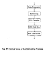
- Fig.11 shows the main steps the compiler must follow to produce code for a system containing a RISC processor and a PACT XPP.
- the next sections focus on the XPP compiler itself, but first the other steps are briefly described.
- This step takes the whole program as input and can be considered as a usual compiler front-end. It will prepare the code by applying code analysis and optimizations to enable the compiler to extract as many loop nests as possible to be executed by the PACT XPP. Important optimizations are idiom recognition, copy propagation, dead code elimination, and all usual analysis like dataflow and alias analysis.
- Partitioning decides which part of the program is executed by the host processor and which part is executed by the PACT XPP.
- a loop nest is executed by the host in three cases:
- a loop nest is said to be well-formed if the loop bounds and the step of all loops are constant, the loop induction variables are known and if there is only one entry and one exit to the loop nest.
- loop tiling allows to overcome this problem, it will be described below. Nevertheless it could be that it is not worth it to execute the loop nest on the PACT XPP if the loop bounds are too low.
- a conditional instruction testing if the loop bounds are large enough can be introduced, and 2 versions of the loop nest are produced. One would be executed on the host processor, and the other on the PACT XPP when the loop bounds are suitable. This would also ease applications of loop transformations, as possible compensation code would be simpler due to the hypothesis on the loop bounds.
- the first one produces code for the host processor and the second one optimizes it further by looking for a better scheduling using software pipelining for instance.
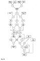
- Fig. 12 describes the internal processing of the XPP Compiler. It is a complex cooperation between program transformations, included in the XPP Loop Optimizations, a temporal partitioning phase, NML code generation and the mapping of the configuration on the PACT XPP.
- First loop optimizations targeted at the PACT XPP are applied to try to produce innermost loop bodies that can be executed on the array of processors. If this is the case, the NML code generation phase is called, if not then temporal partitioning is applied to get several configurations for the same loop. After NML code generation and the mapping phase, it can also happen that a configuration will not fit on the PACT XPP. In this case the loop optimizations are applied again with respect to the reasons of failure of the NML code generation or of the mapping. If this new application of loop optimizations does not change the code, temporal partitioning is applied. Furthermore we keep track of the number of attempts for the NML, Code Generation and the mapping, if too many attempts are made, and we still do not obtain a solution, we break the process, and the loop nest will be executed by the host processor.
- Temporal partitioning splits the code generated for the PACT XPP in several configurations if the number of operations, i.e. the size of the configuration, to be executed in a loop nest exceeds the number of operations executable in a single configuration. This transformation is called loop dissevering [6]. These configurations are then integrated in a loop of configurations whose number of execution corresponds to the iteration range of the original loop.
- This step takes as input an intermediate form of the code produced by the XPP Loop Optimizations step, together with a dataflow graph built upon it. NML code can then be produced by using tree- or DAG-pattern matching techniques.
- This step takes care of mapping the NML modules on the PACT XPP by placing the operations on the ALUs, FREGs, and BREGs, and routing the data through the buses.
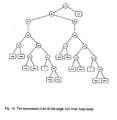
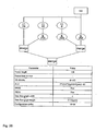
- Fig.13 presents the organization of the loop optimizations.
- the transformations are divided in six groups. Other standard optimizations and analysis are applied in-between. Each group could be called several times. Loops over several groups can also occur if needed.
- the number of iterations for each driver loop can be of constant value or determined at compile time by the optimizations itself (e.g. repeat until a certain code quality is reached). In the first iteration of the loop, it can be checked if loop nests are usable for the PACT XPP, it is mainly directed to check the loop bounds etc.
- Group I ensures that no procedure calls occur in the loop nest.
- Group II prepares the loop bodies by removing loop-invariant instructions and conditional instruction to ease the analysis.
- Group III generates loop nests suitable for the data dependence analysis.
- Group IV contains optimizations to transform the loop nests to get data dependence graphs that are suitable for vectorization.
- Group V contains optimizations that ensure that the innermost loops can be executed on the PACT XPP.
- Group VI contains optimizations that further extract parallelism from the loop bodies.
- Group VII contains optimizations more towards optimizing the usage of the hardware itself.
- loop nests cannot be handled if some dependence distances are not constant, or unknown. If only a few dependences prevent the optimization of the whole loop nest, this could be overcome, by using the traditional vectorization algorithm that sorts topologically the strongly connected components of the data dependence graph (statement reordering), and then apply loop distribution. This way, loop nests, which can be handled by the PACT XPP and some by the host processor, can be obtained.
- Some hardware specific parameters influence the application of the loop transformations. The number of operations and memory accesses, that a loop body performs, is estimated at each step. These parameters influence loop unrolling, strip-mining, loop tiling and also loop interchange (iteration range).
- the table below lists the parameters that influence the application of the optimizations. For each of them two data are given: a starting value computed from the loop, and a restriction value which is the value the parameter should reach or should not exceed after the application of the optimizations.
- Vector length depicts the range of the innermost loops, i.e. the number of elements of an array accessed in the loop body.
- Reused data set size represents the amount of data that must fit in the cache.
- I/O IRAMs, ALU, FREG, BREG stand for the number of IRAMs, ALUs, FREGs, and BREGs respectively that constitute the PACT XPP.
- the dataflow graph width represents the number of operations that can be executed in parallel in the same pipeline stage.
- the dataflow graph height represents the length of the pipeline. Configuration cycles amounts to the length of the pipeline, and to the number of cycles dedicated to the control.
- the application of each optimization may
- Parameter Goal Starting Value Vector length IRAM size (256 words) Loop count Reused data set size Approx. cache size Algorithm analysis/loop sizes T/O IRAMs PACT size (16) Algorithm inputs + outputs ALU PACT size ( ⁇ 64) ALU opcode estimate BREG PACT size ( ⁇ 80) BREG opcode estimate FREG PACT size ( ⁇ 80) FREG opcode estimate Data flow graph width High Algorithm data flow graph Data flow graph height Small Algorithm data flow graph Configuration cycles ⁇ command line parameter Algorithm analysis
- n be the total number of processing elements available, r , the width of the dataflow graph, in , the maximum number of input values in a cycle and out, the maximum number of output values possible in a cycle.
- n is the number of ALUs, FREGs and BREGs available for a configuration
- r is the number of ALUs, FREGs and BREGs that can be started in parallel in the same pipeline stage and, in and out amount to the number of available IRAMs.
- IRAMs have I input port and 1 output port, the number of IRAMs yields directly the number of input and output data.
- the number of operations of a loop body is computed by adding all logic and arithmetic operations occurring in the instructions.
- the number of input values is the number of operands of the instructions regardless of address operations.
- the number of output values is the number of output operands of the instructions regardless of address operations.
- Loop interchange is applied when the innermost loop has a too narrow iteration range. In that case, loop interchange allows to have an innermost loop with a more profitable iteration range. It can also be influenced by the layout of the data in memory. It can be profitable to data locality to interchange two loops to get a more practical way to access arrays in the cache and therefore prevent cache misses. It is of course also influenced by data dependences as explained earlier. Parameter Effect Vector length + Reused data set size make fit I/O IRAMs id ALU id BREG id FREG id Data flow graph width id Data flow graph height id Configuration cycles -
- Loop distribution is applied if a loop body is too big to fit on the PACT XPP. Its main effect is to reduce the processing elements needed by the configuration. Reducing the need for IRAMs can only be a side effect.
- Parameter Effect Vector length id Reused data set size id I/O IRAMs make fit ALU make fit BREG make fit FREG make fit Data flow graph width - Data flow graph height - Configuration cycles -
- Loop collapsing can be used to make the loop body use more memory resources. As several dimensions are merged, the iteration range is increased and the memory needed in increased as well.
- Parameter Effect Vector length + Reused data set size + I/O IRAMs + ALU id BREG id FREG id Data flow graph width + Data flow graph height + Configuration cycles +
- Loop tiling as multi-dimensional strip-mining, is influenced by all parameters, it is especially useful when the iteration space is by far too big to fit in the IRAM, or to guarantee maximum execution time when the iteration space is unbounded (see Section 4.4.6). It can then make the loop body fit with respect to the resources of the PACT XPP, namely the IRAM and cache line sizes.
- the size of the tiles for strip-mining and loop tiling can be computed like this:
- tile size resources available for the loop body / resources necessary for the loop body
- the resources available for the loop body are the whole resources of the PACT XPP for this configuration.
- a tile size can be computed for the data and another one for the processing elements, the final tile size is then the minimum between these two. For instance, when the amount of data accessed is larger than the capacity of the cache, loop tiling can be applied like below.
- Strip-mining is used to make the amount of memory accesses of the innermost loop fit with the IRAMs capacity.
- the processing elements do not usually represent a problem as the PACT XPP has 64 ALU-PAEs which should be sufficient to execute any single loop body. Nevertheless, the number of operations can be also taken into account the same way as the data.
- Parameter Effect Vector length make fit Reused data set size id I/O IRAMs id ALU id BREG id FREG id Data flow graph width + Data flow graph height - Configuration cycles -
- Loop fusion is applied when a loop body does not use enough resources. In this case several loop bodies can be merged to obtain a configuration using a larger part of the available resources.
- the amount of memory needed by the loop body should always fit in the IRAMs. Thanks to this optimization, some input or output data represented by array references, that should be stored in IRAMs, are replaced by scalars, that are either stored in FREGs or kept on buses.
- Loop unrolling, loop collapsing, loop fusion and loop distribution are influenced by the number of operations of the body of the loop nest and the number of data inputs and outputs of these operations, as they modify the size of the loop body.
- the number of operations should always be smaller than n , and the number of input and output data should always be smaller than in and out.
- Unroll-and-Jam consists in unrolling an outer loop and then merging the inner loops. It must compute the unrolling degree u with respect to the number of input memory accesses m and output memory accesses p in the inner loop. The following inequality must hold: u * m ⁇ in ⁇ u * p ⁇ out . Moreover the number of operations of the new inner loop must also fit on the PACT XPP. Parameter Effect Vector length id Reused data set size + I/O IRAMs + ALU + BREG + FREG + Data flow graph width id Data flow graph height + Configuration cycles +
- This optimization deals with array accesses that occur during the execution of a loop body.
- it can be convenient to store them in registers rather than accessing memory each time they are needed.
- a value shares several registers and flows from a register to another at each iteration. It is similar to a vector register allocated to an array access with the same value for each element.
- This optimization is performed directly on the dataflow graph by inserting nodes representing registers when a value must be stored in a register. In the PACT XPP, it amounts to store it in a data register. A detailed explanation can be found in [1].
- Shift register synthesis is mainly suitable for small to medium amounts of iterations where values are alive. Since the pipeline length increases with each iteration for which the value has to be buffered, the following method is better suited for medium to large distances between accesses in one input array.
- This optimization consists in synchronizing operations by inserting delays in the dataflow graph. These delays are registers. For the PACT XPP, it amounts to store values in data registers to delay the operation using them. This is the same as pipeline balancing performed by xmap. Parameter Effect Vector length + Reused data set size id I/O IRAMs id ALU id BREG id FREG id Data flow graph width + Data flow graph height - Configuration cycles +
- This optimization consists in balancing the tree representing the loop body. It reduces the depth of the pipeline, thus reducing the execution time of an iteration, and increases parallelism.
- Parameter Effect Vector length + Reused data set size id I/O IRAMs id ALU id BREG id FREG id Data flow graph width + Data flow graph height - Configuration cycles -
- the execution time of a configuration must be controlled. This is ensured in the compiler by strip-mining and loop tiling that take care that not more input data as the IRAMs capacity come in the PACT XPP in a cycle. This way the iteration range of the innermost loop that is executed on the PACT XPP is limited, and therefore its execution time. Moreover partitioning ensures that loops, whose execution count can be computed at run time, are going to be executed on the PACT XPP. This condition is trivial for for-loops, but for while-loops, where the execution count cannot de determined statically, a transformation like sketched below can be applied. As a result, the inner for-loop can be handled by the PACT XPP.
- the first step normally invokes interprocedural transformations like function inlining and loop pushing. Since no procedure calls are within the loop body, these transformations are not applied to this example.
- the partitioning algorithm chooses which code runs on the RISC processor and which code runs on the XPP. Since we only consider inner loops to run on the XPP, the basic blocks are annotated with the loop nest depth. Thus basic blocks which are not in a loop are separated out. Furthermore function calls within a loop body prevent a loop to be considered for running on the XPP.
- the 'h-loop' is transformed equally, issuing the original code.
- idiom recognition finds the abs() and min() structures in the loop body. Please note that although the XPP has no abs opcode, it can easily be synthesized and should therefore be produced to simplify the internal representation (otherwise if-conversion has to handle this case which increases the complexity).
- the array accesses are mapped to IRAMs.
- the IRAM numbers are chosen arbitrarily, the actual mapping to XPP IRAMs is done later.
- the visualized expression tree in Figure 56 shows another valuable optimization before matching the tree. Since the depth of the tree determines the length of the synthesized pipeline, another simplification can decrease this depth. In both of the main sub trees the operands of the commutative add expressions can be interchanged to reduce the overall tree depth.
- the pipeline is synthesized by a dynamic programming tree matcher. In contrast to sequential processors it does not generate instructions and register references but PAE opcodes and port connections.
- the main calculation network is shown in Figure 58 .
- the input data preparation network is not shown in this figure.
- the case of synthesized shift registers are shown in Fig. 17 . while the variant with duplicated input data simply consists of an IRAM for each input channel in Fig. 16 .
- the configuration calculating the inner loop utilizes 27 ALUs and 4 IRAMs for shift register synthesis and 21 ALUs and 9 IRAMs for data duplication, respectively. Assuming a XPP64 core this leaves plenty of room for further optimizations. Nevertheless, since all optimizations enhancing parallelism are performed before the synthesis takes place, it is crucial that they estimate the needed resources and the benefit of the transformation very carefully. Furthermore they have to account for both input preparation strategies to estimate correct values.
- Loop unrolling the outer loop is also not applicable since it produces a further configuration. Nevertheless a related transformation could do a good job on this loop nest.
- the unroll-and-jam algorithm enhances parallelism and also improves IRAM usage. It brings pairs of iterations together ideally reusing IRAM outputs and calculation results.
- the transformation introduces additional accesses to pl[v+3][h], p1[v+3][h+2], p1[v+3][h+1], and p1[v+1][h+1] (the former hole in the access pattern) as well as a write access to p2[v+2][h+1]. That means 2 IRAMs more for shift register synthesis (one input, one output) and 5 IRAMs more for data duplication (4 input, 1 output), while performance is doubled.
- the simulated results are shown in the table above. Please note the differences of the two columns labeled with "data duplication".
- the second solution improved the iteration cycles by 18. This shows that IRAM placement has a great impact to the final performance.
- the traditional unroll-and-jam algorithm uses loop peeling to split the outer loop in a preloop and an unroll-able main loop to handle odd loop counts.
- the benchmark source code is not very likely to be written in that form in real world applications. Normally it would be encapsulated in a function with parameters for input and output arrays along with the sizes of the picture to work on.
- Strip mining partitions the inner loop into a loop that runs over a strip, which is chosen to be of the same size as the IRAMs can hold and a by strip loop iterating over the strips. Of course the strip loops upper bound must be adjusted for the possible incomplete last strip. After the strip mining the original code would look like (outer v-loop neglected):
- the RISC DSP needs about 1.47 million cycles for this amount of data. As mentioned above these values do not include cache miss penalties and truly underestimate the real values. Furthermore it can be seen that data duplication does not improve the performance. The reason for this seems to be an worse placement and routing.
- the constants N and M are replaced by their values by the pre-processor.
- the data dependence graph is the following:
- the table is the same than before except for the vector length and the expected speedup with respect to a standard superscalar processor with 2 instructions issued per cycle is 17.5.
- the parameter table given below corresponds to the two inner loops in order to be compared with the preceding table.
- the case of the second loop is trivial, it does not need to be strip-mined either.
- the second loop is a reduction, it computes the sum of a vector. This is easily found by the reduction recognition optimization and we obtain the following code.
- the drawback of this solution is that it uses 16 IRAMs, and that the input data must be stored in a special order.
- the number of needed IRAMs can be reduced if the coefficients are handled like constant for each ALU.
- the parameter table is then the following: Parameter Value Vector length 249 Reused data set size - I/O IRAMs 16 ALU 15 BREG 0 FREG 0 Data flow graph width 8 Data flow graph height 4 Configuration cycles 4+961
- the data dependence graph is the same as above. We apply then node splitting to get a more convenient data dependence graph.
- IRAMs are used in FIFO mode, and filled according to the addresses of the arrays in the loop.
- IRAM0, IRAM2, IRAM4, IRAM6 and IRAM8 contain array c.
- IRAM 1, IRAM3, IRAM5 and IRAM7 contain array x .
- Array c contains 64 elements, that is each IRAM contains 8 elements.
- Array x contains 1024 elements, that is 128 elements for each IRAM.
- Array y is directly written to memory, as it is a global array and its address is constant. This constant is used to initialize the address counter of the configuration.
- the data dependency graph shows no dependencies that prevent pipeline vectorization.
- the loop carried true dependence from S2 to itself can be handled by a feedback of aux as described in [1].
- Finding the best loop nest is relatively simple.
- the algorithm simply interchanges each loop of the nests into the innermost position and annotates it with the so-called innermost memory cost term.
- This cost term is a constant for known loop bounds or a function of the loop bound for unknown loop bounds. The term is calculated in three steps.
- the table shows the values for the matrix multiplication. Since the j term is the smallest (of course assuming b > 1), the j-loop is chosen to be the innermost. The next outer loop then is k, and the outermost is i. Thus the resulting code after loop interchange is
- Fig. 22 shows the improved iteration spaces. It is to say that this optimization does not optimize primarily for the XPP, but mainly optimizes the cache-hit rate, thus improving the overall performance.
- the constraint generated by the IRAMs therefore dominates by far.
- the innermost loop can be synthesized in a configuration, which uses 14 IRAMs for the input data, one IRAM to temporary store aux and one IRAM for the output array R. Furthermore it is necessary to pass the value of k to the XPP to direct the dataflow. This may be done by a streaming input.
- Fig. 23 shows the dataflow graph of the synthesized configuration.
- the following code shows the pseudo code executed on the RISC processor.
- the table shows the simulated configuration.
- the complete multiplication needs about 3120 cycles without the preloading and configuration.
- a typical RISC-DSP core with two MAC units and hardware loop support needs over 26000 cycles (when data is in zero-latency internal memory).
- the time for preloads and cache misses is neglected here, the values promise improvements of 200-300 percent compared to a standalone RISC core:
- Parameter Value Vector length 20 Reused data set size 20 I/O IRAMs 14 I + I O + I internal ALU 20 BREG 26 (8 defined + 18 route) FREG 28(4 defined + 24 route)
- Data flow graph width 14
- the first loop (setting vp->dp->w[0..7] to zero) is most efficiently executed on the RISC.
- the second loop (with the BFLY() macro expanded) is of interest for the XPP compiler and needs further examination:
- the data flow graph is as follows (for now ignoring the fact, that the IRAM accesses are mostly char accesses).
- the solid lines represent data flow, while the dashed lines represent event flow:
- IRAM7 is fully busy reading and rewriting the same address sixteen times. Loop tiling to a tile size of sixteen gives the redundant load store elimination a chance to read the value once and accumulate the bits in the temporary, writing the value to the IRAM at the end of this inner loop. Loop Fusion with the initialization loop then allows propagation of the zero values set in the first loop to the reads of vp->dp->w[i] (IRAM7), eliminating the first loop altogether.
- Loop tiling with a tile size of 16 also eliminates the & 31 expressions for the shift values: Since the new inner loop only runs from 0 to 16, the value range analysis now finds that the & 31 expression is not limiting the value range any further.
- IRAMs All remaining input IRAMs are character (8 bit) based. So we need split networks to split the 32-bit stream into four 8-bit streams which are then merged. This adds 3 shifts, 3 ands and 3 merges for every character IRAM. The merges could be eliminated, when unrolling the loop body. However, unrolling is limited to unrolling twice due to ALU availability as well as due to the fact, that IRAM6 is already 16 bit based: unrolling once requires a shift by 16 and an or to write 32 bits in every cycle; unrolling further cannot increase pipeline throughput any more. So the body is only unrolled once, eliminating one layer of merges. This yields two separate pipelines, that each handle two eight bit slices of the 32-bit value from the IRAM, serialized by merges.
- the Normalization consists of a loop scanning the input for the minimum and a second loop that subtracts the minimum from all elements. There is a data dependency between all iterations of the first loop and all iterations of the second loop. Therefore the two loops cannot be merged or pipelined.
- the third loop is a minimum search on a byte array.
- Reduction recognition eliminates the dependence for minmetric enabling a four-times unroll to utilize the IRAM width of 32 bits.
- a split network has to be added to separate the 8 bit streams using 3 SHIFT and 3 AND operations.
- Tree balancing re-distributes the min() operations to minimize the tree height.
- the fourth loop subtracts the minimum of the third loop from each element in the array.
- the read-modify-write operation has to be broken up into two IRAMs. Otherwise the IRAM ports will limit throughput.
- Unroll and jam can be applied after loop tiling, in analogy to the third loop, but loop tiling is now limited by the BREGs used by the split and join networks.
- Performance of XPP for this example is compared to a hypothetical superscalar RISC-architecture.
- We Operation Cycles Bfly Setup Butterfly Min Setup Min Search Norm Setup Normalize ADRCOMP 1 6 7 1 LD/ST 2 5 8 2 1 2 LDI 1 3 4 1 1 MOVE 1 4 1 BITOP 1 10 ADD/SUB 1 20 3 1 3 MULT 2 2 CJMP 3 3 2 1 Cycles 23 70 5 11 4 10 Count 1 128 1 64 1 64 Issue Width 2 Est RISC cycles Total Cycles 12 4480 3 352 2 320 5168 RISC Cycles assume an average issue width of two which means that the RISC on average executes two operations in parallel. The estimate is achieved by counting instructions for the source code in 5.4.2.
- the quantization file contains routines for quantization and inverse quantization of 8x8 macro blocks. These functions differ for intra and non-intra blocks and furthermore the encoder distinguishes between MPEG1 and MPEG2 inverse quantization.
- the j-i loop nest is a candidate for unroll-and-jam when the interprocedural value range analysis finds out that block_count can only get the values 6,8 or 12. Therefore it has a value range [6,12] with the additional attribute to be dividable by 2. Thus an unroll and jam with the factor 2 is applicable (the resource constraints would choose a bigger value). Since no loop carried dependencies exist, this transformation is safe.
- the source code contains a manually peeled first iteration. This peeling has been done because the value calculated for the first block value is completely different from the other iterations and the control statement in the loop would cause a major performance decrease on traditional processors. Although this does not prevent unroll-and-jam (because there are no dependencies between the peeled of first iteration and the rest of the loop), the transformation must be prepared to handle such cases.
- index set splitting Normally used to break dependence cycles in the DDG, it can here be used to split the i-loop in two and let two sub-configurations work on distinct blocks of data. Thus the i loop is split into 2 or more loops which work on different subsets of the data at the same time. 5 sub-configuration is chosen as a working title for configurations which contains independent networks that do not interfere.
- the MPEG2 codec uses all data types commonly used on a processor for desktop applications.
- the sizes of char, short and int are 8,16, and 32 respectively.
- the XPP has a bit width of 32 we must take precautions for the smaller data types.
- Figure 65 shows how the merge is done. Instead of streaming parallel through two networks the values are serialized and de-serialized again after the network.
- the idct-algorithm is used for the MPEG2 video decompression algorithm. It operates on 8x8 blocks of video images in their frequency representation and transforms them back into their original signal form.
- the MPEG2 decoder contains a transform-function that calls idct for all blocks of a frequency-transformed picture to restore the original image.
- the idct function consists of two for-loops.
- the first loop calls idctrow - the second idctcol.
- Function inlining is able to eliminate the function calls within the entire loop nest structure so that the numeric code is not interrupted by function calls anymore.
- Another way to get rid of function calls between the loop nest is loop embedding that pushes loops from the caller into the callee.
- the first loop changes the values of the block row by row. Afterwards the changed block is further transformed column by column. All rows have to be finished before any column processing can be started.
- Fig. 29
- idctrow and idctcol are nearly identical. They process numeric calculations on eight input values (column values in case of idctcol and row values in case of idctcol). Eight output values are calculated and written back (as column/row). Idctcol additionally applies clipping before the values are written back. This is why we concentrate on idctcol:
- W1 - W7 are macros for numeric constants that are substituted by the preprocessor.
- the iclp array is used for clipping the results to 8-bit values. It is fully defined by the init_idct function before idct is called the first time:
- a special kind of idiom recognition is able to replace the calculation of each array element by a compiler known function that can be realized efficiently on the XPP. If the compiler features whole program memory aliasing analysis it is able to replace all uses of the iclp array with the call of the compiler known function. Alternatively a developer can replace the iclp array accesses manually by the compiler known saturation function calls.
- the illustration shows a possible implementation for saturate(val,n) as NML schematic using two ALUs. In this case it is necessary to replace array accesses like iclp[i] by saturate(i,256).
- the /*shortcut*/ code in idctcol speeds column processing up ifxl to x7 is zero. This breaks the well-formed structure of the loop nest.
- the if-condition is not loop invariant and loop unswitching cannot be applied. But nonetheless - the code after shortcut handling is well suited for the XPP. It is possible to synthesize if-conditions for the XPP (speculative processing of both blocks plus selection based on condition) but this would just waste PAEs without any performance benefit. Therefore the /*shortcut*/ code in idctrow and idctcol has to be removed manually.
- the code snippet below shows the inlined version of the idctrow-loop with additional cache instructions for XPP control:
- idctcol is more complex due to clipping at the end of the calculations we decided to take idctcol as representative loop body for a presentation of the data flow graph.
- the figure on the next page shows the data flow graph for the IDCTCOLUMN CONFIG.
- a heuristic has to be applied to the graph to estimate the resource needs on the XPP.
- the heuristic produces the following results: ADD,SUB MUL ⁇ X,>> X Saturate(x,n) Ops needed 35 11 18 8 ALUs FREGs BREGs Res. left 19 80 45 Res. avail. 64 80 80 80 80
- Fig. 32 For IDCTCOLUMN CONFIG we have to select the n th element of every row which means an address serial of (0,8,16...1,9,17... 7,15,23). We use two counter macros for address generation as shown opposite. The upper counter increments by eight and the lower by one. The IRAM output is passed to the data How graph of IDCTCOLUMN. If all (eight) row elements of a column are available SWAP is switched through to the data flow graph input and the calculation for a new column begins.
- IDCTROW_CONFIG For the IDCTROW_CONFIG the address generation is very simple as the IRAM already contains the block in the appropriate order (row after row as it has to be accessed). Again by using SIUP(stepped iterative up)-counter macros as described in the XPP tutorial it is possible to map linear address expressions to NML-code in a generic way. As IDCTROW_CONFIG accesses a two-dimensional array we need two SIUP-counters in the corresponding NML code. The column-elements have to be accessed row after row so the upper counters increment is one and the lower counters increment is eight. However, the NML code for this access pattern (0...,5,6,7,8,9,...63) can be reduced to one single counter (or to FIFO-mode IRAM access).
- Address generation for write access is implemented in the same manner.
- the resources have to be updated to take this additional code into account. It takes 2*(8+8+2*1) FREGs and 2*(2+1) more BREGs in the worst case which is stilt available on the XPP.
- IRAM use is not critical it is also possible to distribute the data on several IRAMs to improve the memory throughput into the XPP-array. This task has to be done by the RISC-core or by a more sophisticated XPP-cache controller.
- the pipeline is just too deep for processing only eight times eight rows. Filling and flushing a deep pipeline is expensive if only little data is processed with it. First the units at the end of the pipeline are idle and then the units at the begin are unused.
- IDCTROW_CONFIG and IDCOLUMN_CONFIG has to be modified for reflecting the different data block size - caused by loop tiling - that has to be processed. This can be implemented by an additional SUIP counter that generates the block offsets inside the tiles.
- the table contains architectural parameters for IDCTROW_CONFIG and IDCOLUMN_CONFIG of the final result It relies on a cache that is able to store block_count blocks.
- the configuration cycles have to be taken twice and therefore the total configuration cycles are 2 x (block-count x 64 + (12 + 2 x 8) x 2).
- Parameter Value Vector length 8 words Reused data set size block_count x 64 words I/O IRAMs 3 (one shared)
- ALU 45 FUs BREG 41 FUs FREG 36 FUs
- Full utilization can be achieved only by loading the eight input values of the pipeline in one cycle.
- a simple solution to improve the memory throughput to the pipeline is data duplication as described in the hardware section.
- the two inner loops do not have the same iteration range and could be candidate for loop fusion, therefore the first and last iterations of the second loop are peeled off.
- the surrounding code between the 2 loops can be moved after the second loop, then we obtain the following code for the loop nest.
- nt ranges takes the values 64, 32 and 16.
- the upper bound of the inner loops is mid, which depends on the value of nt .
- the analysis finds then that mid can take the values: 31, 15 and 7.
- Loops with constant loop bounds can be handled more efficiently on the PACT XPP. This means that the inner loops can be better optimized if mid is replaced by a constant value. This will happen when the outer loop is unrolled. This way we will obtain a bigger code, but with 3 instances of the loop nest, each being candidate for a configuration. This can be seen as a kind of temporal partitioning. Thus the outer loop is completely unrolled giving six new loop nests.
- the vector length is the only value that change. We give it for the first two loops. To deduce the table for the other loops, the vector length has to be set to 14 and 6 respectively.
- Each input and output data will occupy an IRAM.
- d 0 a nd s0 will be the only values in their IRAM, enabling then the merge operations to select between d0 , resp. s0 at the first iteration and the feedback values for the other iterations.
- 8 values can be output in a cycle, corresponding to 4 values for array x.
- the same configuration is used for all loops; only the data in the IRAMs differ.
- a new approach of a flexible and high performance datapath concept is needed, which allows to reconfigure the functionality and make this core mainly application independent without losing the performance needed for stream-based applications.
- This microprocessor is a synthesisable, free available VHDL model which has a load/store architecture and has a five stages pipeline implementation with seperated instruction and data caches.
- the LEON is provided with a full implementation of AMBA 2.0 AHB and APB on-chip bus, a hardware multiplier and devider, programmable 8/16/32-bit memory controller for external PROM, static RAM and SDRAM and several on-chip peripherals such as timers, UARTs, interrupt controller and a 16-bit I/O port.
- a simple power down mode is implemented as well.
- LEON is developed by the European Space Agency (ESA) for future space missions.
- ESA European Space Agency
- the performance of LEON is close to an ARM9 series but don't have a memory management unit (MMU) implementation, which limits the use to single memory space applications.
- MMU memory management unit
- Fig.40 the datapath of the LEON integer unit is shown.
- the XPP architecture [6], [7], [8] is based on a hierarchical array of coarse-grain, adaptive computing elements called Processing Array Elements (PAEs) and a packet-oriented communication network.
- PAEs Processing Array Elements
- the strength of the XPP technology originates from the combination of array processing with unique, powerful run-time reconfiguration mechanisms. Since configuration control is distributed over a Configuration Manager (CM) embedded in the array, PAEs can be configured rapidly in parallel while neighboring PAEs are processing data. Entire applications can be configured and run independently on different parts of the array. Reconfiguration is triggered externally or even by special event signals originating within the array, enabling self-reconfiguring designs. By utilizing protocols implemented in hardware, data and event packets are used to process, generate, decompose and merge streams of data.
- CM Configuration Manager
- the XPP has some similarities with other coarse-grain reconfigurable architectures like the KressArray [3] or Raw Machines [4]. which are specifically designed for stream-based applications.
- XPP's main distinguishing features are its automatic packet-handling mechanisms and its sophisticated hierarchical configuration protocols for runtime- and self-reconfiguration.
- a CM consists of a state machine and internal RAM for configuration caching.
- the PAC itself (see top right-hand side of Figure 69) contains a configuration bus which connects the CM with PAEs and other configurable objects.
- Horizontal busses carry data and events. They can be segmented by configurable switch-objects, and connected to PAEs and special I/O objects at the periphery of the device.
- a PAE is a collection of PAE objects.
- the typical PAE shown in Figure 69 (bottom) contains a BREG object (back registers) and an FREG object (forward registers) which are used for vertical routing, as well as an ALU object which performs the actual computations.
- the ALU performs common fixed-point arithmetical and logical operations as well as several special threeinput opcodes like multiply-add, sort, and counters. Events generated by ALU objects depend on ALU results or exceptions, very similar to the state flags of a classical microprocessor.
- a counter e.g., generates a special event only after it has terminated. The next section explains how these events are used.
- Another PAE object implemented in the XPP is a memory object which can be used in FIFO mode or as RAM for lookup tables, intermediate results etc. However, any PAE object functionality can be included in the XPP architecture.
- PAE objects as defined above communicates via a packet-oriented network. Two types of packets are sent through the array: data packets and event packets. Data packets have a uniform bit width specific to the device type. In normal operation mode, PAE objects are selfsynchronizing. An operation is performed as soon as all necessary data input packets are available. The results are forwarded as soon as they are available, provided the previous results have been consumed. Thus it is possible to map a signal-flow graph directly to ALU objects. Event packets are one bit wide. They transmit state information which controls ALU execution and packet generation.
- Every PAE stores locally its current configuration state, i.e. if it is part of a configuration or not (states “configured” or “free”). Once a PAE is configured, it changes its state to "configured”. This prevents the CM from reconfiguring a PAE which is still used by another application.
- the CM caches the configuration data in its internal RAM until the required PAEs become available.
- NML Native Mapping Language
- configurations consist of modules which are specified as in a structural hardware description language, similar to, for instance, structural VHDL, PAE objects are explicitly allocated, optionally placed, and their connections specified. Hierarchical modules allow component reuse, especially for repetitive layouts. Additionally, NML includes statements to support configuration handling.
- a complete NML application program consists of one or more modules, a sequence of initially configured modules, differential changes, and statements which map event signals to configuration and prefetch requests. Thus configuration handling is an explicit part of the application program.
- the system is designed to offer a maximum of performance.
- LEON and XPP should be able to communicate with each other in a simple and high performance manner. While the XPP is a dataflow orientated device, the LEON is a general purpose processor, suitable for handling control flow [1], [2]. Therefore, LEON is used for system control. To do this, the XPP is integrated into the datapath of the LEON integer unit, which is able to control the XPP.
- Dual-clocked FIFOs are implemented into the IO-Ports between LEON and XPP.
- the IO-Ports contain logic to generate handshake signals and an interrupt request signal.
- the IO-Port for receiving data from XPP is similar to Figure 5 except that the reversed direction of the data signals.
- XPP can generate interrupts for the LEON when trying to read a value from an empty FIFO port or to write a value to a full FIFO port.
- the occurrence of interrupts indicates, that the XPP array cannot process the next step because it has either no input values or it cannot output the result value.
- the interrupts generated by the XPP are maskable.
- the interface provides information about the FIFOs. LEON can read the number of valid values the FIFO contains.
- the interface to the XPP appears to the LEON as a set of special registers. ( Figure 6 ). These XPP registers can be categorized in communication registers and status registers.
- XPP For data exchange the XPP communication registers are used. Since XPP provides three different types of communication ports, there are also three types of communication registes, whereas every type is splitted into an input part and an output part:
- the data for the process are accessed through XPP data registers.
- the number of data input and data output ports as well as the data bit-width depends on the implemented XPP array.
- XPP can generate and consume events. Events are one bit signals. The number of input events and output events depends on the implemented XPP array again.
- Configuration of the XPP is done through the XPP configuration register. LEON reads the required configuration value from a file - stored in his system RAM - and writes it to the XPP configuration register.
- a XPP clock register contains a clock frequency ratio between LEON and XPP. By writing this register LEON software can set the XPP clock relative to LEON clock. This allows to adapt the XPP clock frequency to the required XPP performance and consequently to influence the power consumption of the system. Writing zero to the XPP clock register turns off the XPP. At last there is a status register for every FIFO containing the number of valid values actually available in the FIFO.
- This status registers provides a maximum of felxibility in communication between LEON and XPP and enables different communication modes:
- the XPP is delivered containing a configuration manager to handle configuration and reconfiguration of the array.
- the configuration manager is dispensable because the configuration as well as any reconfiguration is controlled by the LEON through the XPP configuration register. All XPP configurations used for an application are stored in the LEON's system RAM.
- the LEON's SPARC 8 instruction set [1] was extended by a new subset of instructions to make the new XPP registers accessable through software. These instructions are based in the SPARC instruction format but they are not conform to the SPARC V8 standard. Corresponding to the SPARC conventions of a load/store Architecture the instruction subset can be splitted in two general types. Load/store instructions can exchange data between the LEON memory and the XPP communication registers. The number of cycles per instruction are similar to the standard load/store instructions of the LEON. Read/write instructions are used for communications between LEON registers. Since the LEON register-set is extended by the XPP registers the read/write instructions are extended also to access XPP registers. Status registers can only be accessed with read/write instructions. Execution of arithmetic instructions on XPP registers is not possible. Values have to be written to standard LEON registers before they can be target of arithmetic operations.
- the complete system can still operate any SPARC V8 compatiple code. Doing this, the XPP is completely unused.
- the LEON is provided with the LECCS cross compiler system [9] standing under the terms of LGPL.
- This system consists of modified versions of the binutils 2.11 and gcc 2.95.2.
- the assembler of the binutils has been extended by a number of instructions according to the implemented instruction subset.
- the new instructions have the same mnemonic as the regular SPARC V8 load, store, read and write instructions. Only the new XPP registers have to be used as source respectively target operand. Since the modifications of LECCS are straightforward extensions, the cross compiler system is backward compatible to the original version. The availability of the source code of LECCS has allowed to extend the tools by the new XPP operations in the described way.
- a first complex application implemented on the system is MPEG-4 decoding.
- the optimization of the algorithm partitioning on LEON and XPP is still under construction.
- Figure 8 the blockdiagram of the MPEG-4 decoding algorithm is shown. Frames with 320 x 240 pixel was decoded. LEON by using SPARC V8 standard instructions decodes one frame in 23,46 seconds.
- the IDCT is computed by XPP
- the rest of the MPEG-4 decoding is still done with LEON.
- XPP one frame is decoded in 17,98 s. This is a performance boost of more then twenty percent.
- the introduced coupling technique by flexible dual-clock FIFO interfaces allows asynchronous concurrency and adapting the frequency of the configured XPP datapath dependent on actual performance requirements, e.g. for avoiding unneeded cycles and reducing power consumption.
- the introduced concept combines the flexibility of a general purpose microprocesser with the performance and power consumption of coarse-grain reconfigurable datapath structures, nearly comparable to ASIC performance.
- two programming and computing paradigms control-driven von Neumann and transport-triggered XPP
- the ability to reconfigure the transport-triggered XPP makes the system independent from standards or specific applications.
- This concept opens potenial to develop multi-standard communication devices like software radios by using one extended processor architecture with adapted programming and compilation tools.
- new standards can be easily implemented through software updates.
- the system is scalable during design time through the scalable array-structure of the used XPP extension. This extends the range of suitable applications from products with less multimadia functions to complex high performance systems.
- This aspect deals with problems relating to the implementation of hyper-threading, multi-threading, multi-tasking, scheduling and execution of parts of configurations and so forth.
- WO 00/49496 already discloses a method for execution of a computer program, using a processor comprising a configural functional unit capable of executing reconfigurable instructions in fact of which can redefined at runtime.
- the data processing logic cell field is practically used to allow for user-defined opcodes that can process data more efficiently than is possible on the ALU of the CPU without further support by the data processing logic cell field.
- the coupling is generally word-based, not block-based. It is a further important aspect of the present invention that is has been realized that for data-streaming data-processing block-based coupling is highly preferable. At any rate, a more efficient data processing, in particular more efficient than possible with a close coupling via registers, is highly preferable.
- Another method for the use of logic cell fields consisting of coarse- and/or fine-granular logic cells and logic cell elements consists in a very loose coupling of such a field to a conventional CPU and/or a CPU-core in embeded systems.
- a conventional sequential program can be executed on the CPU, for example a program written in C, C++ or the like, wherein the instantiation of the data stream processing by the fine- and/or coarse-granular data processing logic cell field is effected via that sequential program. Then, the problem exists that in programming said logic cell field a program not written in C or any other sequential high-level language must be provided for the data stream processing.
- time use planning control means and -methods are known per se, that, at least under a corresponding interrelation of configurations and/or assignment of configurations to certain tasks and/or threads to configurations and/or sequences of configurations allow for a multi-tasking and/or multi-threading.
- time use planning control means used in the prior art for configuring and management of configurations for the purpose of scheduling of tasks, threads, multi- and hyper-threads is considered to be inventive per se.
- Another important aspect of the present invention can be seen in that data are inputted into that data processing logic cell fields in response to the execution of a load configuration by that data processing logic cell fields and/or in that data are stored from that data processing logic cell fields by executing a store-configuration. Accordingly, it is preferred to provide the load- and/or store-configurations in such a way that the addresses of those memory cells used are directly or indirectly generated within the data processing logic cell fields, the addresses indicating those memory cells and/or locations to which an access has to be effected as load- and/or store-access, that is as a read- and/or write-access.
- the data loading can take place, provided that that logic cell fields are, as is typically the case, sufficiently large, in small partial areas thereof, while other partial areas are executing other tasks.
- that known ping-pong-like data processing relying on memory cells provided on each side of that data processing field, where data in a first data processing step stream from the memory on one side through the data processing field to the memory on the other side of that data processing field, where they are stored as intermediate results while, if necessary, the array is reconfigured, the intermediate results are then streaming back for further processing and so forth.
- a memory strip on one side and/or memory part on one side can be preloaded with data by a load-configuration in one array part while on the memory part on the other side of the logic cell field data are written out using a store-configuration. It is to be noted that such a simultaneous load-/store-way of data processing is possible even without spatial distribution and/or separation of memory areas in which data are retrieved and/or in which data are stored.
- This cache-coupling is also highly preferred compared to the coupling of the data processing logic cell field to the ALU with the CPU via registers, if those registers communicate only via a load-/store-unit with the cache as is known in the non-PACT prior art.
- the logic cells of that field can comprise ALUs or EALUs respectively which can have at their input- and/or output ports short, fine-granularly configurably FPGA-like circuitries, for example to cut out 4-bit-blocks out of a continous data stream as is necessary for example for an MPEG-4-decoding.
- ALUs or EALUs respectively which can have at their input- and/or output ports short, fine-granularly configurably FPGA-like circuitries, for example to cut out 4-bit-blocks out of a continous data stream as is necessary for example for an MPEG-4-decoding.
- the ALU is provided as a SIMD-ALU; here, for example, a very broad data word having for example 32-bit-data-width is split via an FPGA-like stripe in front of the SIMD-ALU splitting the broad e. g. 32-bit-data into eight data words having for example 4-bit-data-width that can then be processed parallelly in the SIMD-ALU increasing the overall performance of the system significantly provided that the respect of applications are needed.
- FPGA-like pre- or post that structures it is not absolute necessary to refer to 1-bit-granular devices; in contrast, it would be possible to provide finer-granular structures of a for example 4-bit- instead of the hyper-fine-granular 1-bit-structures.
- the FPGA-like input- and/or output-structures in front of or data downstream of that ALU-unit, in particular SIMD-ALU-units are configurable in such a way that always 4-bit-data-words are processed.
- every single thread can be assigned a separate slice thus allowing that on processing that thread the respective cache areas are accessed on the re-entry of the group of codes to be processed.
- the cache needs not necessarily be separated into slices and that, even if the cache is separated into slices, not every single thread must be assigned a separate slice.
- this is a higly preferred method.
- certain cache-areas can be separated from the power source in such a way that the energy consumption is significantly reduced, in particularly close to or exactly to 0.
- power supply separation means adapted to separate cache slices from power.
- the separation can either be effected by a down-clocking, separation of clock-lines and/or the overall separation of a power supply. It is in particular possible to provide for such a separation for every single cache slice, for example by an access identification adapted to identify whether or not a thread, hyper-thread, task or the like is currently assigned to a respective cache slice.
- the access identification means indicates and/or detects that this is not the case, typically a separation of the slice from a clock-line and/or even the power-line can be envisaged as possible. It is also to be noted that on repowering-up after a separation from power it is possible to immediately access the cache area, thus, no significant delay by switching an ON or OF of the power is to be expected, as long as the hardware is implemented with current semiconductor technologies.
- a further particular advantage of the prevent invention resides in the fact that although the transfer of data and/or operands is possible in a block-wise manner, no particular balancing is needed to ensure that exactly the same times of execution of data processing steps in the sequential CPU and the XPP and/or other data processing logic cell fields are achieved. Instead, the processing is frequently independent, in particular in such a way that the sequential CPU and the data processing logic cell field can be considered as separate resources by a scheduler. This allows for the immediate implementation of known data processing programs splitting technologies such as multi-tasking, multi-threading, hyper-therading.
- a further advantage of the present invention results in that by configuring a load- and a store-configuration into the data processing logic cell fields the data inside the field can be loaded into that field or out of that field which is no more controlled by the clock frequency of the CPU, the performance of the opcode fetcher and so forth. In other words, the opcode fetcher is no more bottle-necking the data throughput to the data logic cell field without having an only loose coupling.
- CT or CM commonly employed in the XPP-unit, also given the fact that with one or more, even hierarchically arranged XPP-fields having in preferred embodiments their own CTs while simultaneously using one or more sequential CPUs
- CT or CM commonly employed in the XPP-unit, also given the fact that with one or more, even hierarchically arranged XPP-fields having in preferred embodiments their own CTs while simultaneously using one or more sequential CPUs
- FILMO and so forth become applicable for the hardware support and management of hyper-threading and so forth
- Cache coupling and/or load and/or store configurations providing addresses generators for loading and/or storing of data into that data processing logic cell field or out of that field will provide for the data exchange of the XPP.
- the coprocessor-like coupling to the data processing logic cell field is enabled while simultaneously a data stream-like data loading is effected via cache- and/or I/O-port coupling.
- the method of coprocessor coupling that is the indicated coupling of the data processing logic cell field will typically result in the scheduling of that logic cell field taking place on the sequential CPU and/or a supervising scheduler unit and/or a respective scheduler means.
- the threading control and/or -manage-ment practically takes place on the scheduler and/or the sequential CPU.
- the data processing logic cell field can be called in a conventional manner, such as has been the case in a standard coprocessor such as a combination of 8086/8087.
- the configuration manager acting as scheduler at the same time or in any other way it is possible to addresss memory within or in immediate vicinity of the data processing logic cell fields or under its management, in particular memory within the XPP-architecture as is known by the applicant, RAM-PAEs or other; accordingly managing internal memories such as a vector register is suggested, that is the data volumes loaded via the load configuration are stored vector-like in vector registers in the internal memory-cells, thereafter accessing said registers after loading and/or activating of a new configuration for effecting the actual data processing.
- a data processing configuration can be referred to as one configuration even in case that several distinct configurations are to be processed simultaneously, one after the other or in a wave-like modus.
- a vector register can be used to store results and/or intermediate results in the internal or internally managed memory cell elements.
- the vector register-like accessed memory means in the XPP can be used also, after reconfiguration of the processing configuration by loading a store configuration in a suitable manner in a way that takes place again in a data-stream-like manner, be it via an I/O-port directly streaming data into external memory areas and/or, as particularly preferred, into cache areas or out of these which then can be accessed at a later stage by the sequential CPU and/or other configurations executed on the other data processing logic cell field, in particularly a data processing logic cell field having produced said data in the first place.
- the memory and/or memory register means into which that data processed are to be stored not an internal memory, but instead a cache area having access reservation, in particularly cache areas which are organized in a slice-wise manner can be used.
- This can have the disadvantage of a larger latency, in particular if the paths between the XPP and/or data processing logic cell fields to or from the cache are of considerable length such that signal transmission delays need to be considered. Still this allows to avoid additional store configurations.
- the cache controller of the known sequential CPU addresses as a cache a memory area that without serving for the purpose of data exchange with a data processing logic cell field is physically placed onto that data processing logic cell field and/or close to that field.
- This is advantageous in that, if applications are run onto the data processing logic cell fields having a very small local memory need and/or if only few other configurations compared to the overall amount of memory space available are needed, these memory areas can be assigned to one or more sequential CPUs as cache or additional cache.
- the cache controller may be adapted for the management of a cache area having a dynamically varying size.
- a dynamical cache-size management and/or dynamical cache management size means for the dynamical cache management may particularly take into account the work load on the sequential CPU and/or the data processing logic cell fields. In other words, it could be analyzed for example how many NOPs in a given time unit are executed on the sequential CPU and/or how many configurations are preloaded in the dynamically reconfigurable field in the memory areas provided therefore, so as to enable fast reconfiguration (be it by the way of wave-reconfiguration or in any other way).
- the dynamical cache size or cache size management disclosed herewith is, in a highly preferred manner, runtime dynamical, that is, the cache controller controls a momentary cache size respectively that can be changed from clock-cycle to clock-cycle or from one group of clock-cycles to the other.
- a configuration management unit can be provided, it is now to be explicitly noted that such units and their way of operation allowing in particular the preloading or configurations currently not yet needed can be used very easily to effect the multi-task operation and/or hyper-threading and/or multi-threading, in particular for task- and/or thread- and/or hyper-thread switches.
- a thread or a task it is possible to preload configurations for different tasks and/or threads and/or hyper-threads into the PAE-array.
- the configuration manager When using a pure sequential CPU and/or several pure sequential CPUs, the configuration manager thus also acts as and realizes a hyper-threading management hardware. Reference is being had to DE 198 07 872 , WO 99/44147 and WO 99/44120 . It can be considered as sufficient, in particular in case where the CPU and/or several sequential CPUs shall have a hyper-threading management to keep partial circuitry elements such as the FILMO, described in the documents referred to.
- the plurality of CPUs can be realized with known techniques such as known for example from DE 102 12 621 , PCT/EP 02/10572 . It is also to be noted that DE 106 51 075 , DE 106 54 846 , DE 107 04 728 ; WO 98/26356 , WO 98/29952 und WO 98/35299 disclose how to implement sequencers having ring- and/or random-access memory means in data processing logic cell fields.
- a task-, thread- and/or hyper-thread switch respectively can be effected with the known CT-technolgy such that performance-slices and/or time-slices are assigned to a software implemented operating system scheduler by the CT, during which slices it is determined which parts of tasks and/or threads are subsequently to be executed provided that resources are available.
- an address sequence is generated for a first task during which the execution of a load configuration loads data from a cache memory coupled with to the data processing logic cell field in the described manner.
- the execution of a second the actual data processing configuration can be started.
- This configuration can be preloaded as well, since it is certain that this configuration is to be executed provided that no interrupts or the like cause task switchs.
- a test can be made whether or not the respective date have been streamed into the array, e. g. checking if the latency time which typically occurs has lapsed and/or the data are actually present.
- latency times which occur as configurations are not yet preloaded, data have not yet been loaded and/or data have not yet been stored, are bridged and/or covered by executing threads, hyper-threads and/or tasks which have been preconfigured and which process data that are already available or can be written to resources that are available for writing thereto.
- latency times are covered and/or bridged and, provided a sufficient number of threads, hyper-threads and/or tasks are to be executed, the data processing logic cell field will have almost 100 % load.
- a task switch in such systems capable of real time processing will thus typically be possible in one of three ways namely either when a task has run for a certain time (watch dog-principle), not-availability of a resource, be it due to a blockade due to another access or due to latencies and/or in the case of the occurrence of interrupts.
- a way of implementing one of these variants may ensure the real time capability.
- one resource which is under the control of the CT oder scheduler switches over to processing the interrupt. If the allowed response time to a certain interrupt is so long that the configuration currently configured can be executed without interruption this is uncritical, particular in view of the fact that the interrupt handling configuration can be preloaded.
- the selection of the interrupt handling configuration to be preloaded can be carried out by the CT or any other instance. It is also possible, to restrict the runtime of the configuration on the resource to which the interrupt processing has been assigned. Reference is being had to PCT/DE 03/000942
- a particular preferred embodiment of a reaction to an interrupt consists in using interrupt routines where code for the data processing logic cell field is forbidden, this embodiment being preferred when one of the resources available is a sequential CPU.
- an interrupt handling routine is executed only on a sequential CPU without calling data processing steps or routines making use of a data processing logic cell field. This guarantees that the processing on the data processing logic cell field is not to be interrupted and then, further processing on that data processing logic cell field can be effected following a task switch.
- the actual interrupt routine does not comprise any data processing logic cell field code such as XPP-code, it can still be made sure that at a later time no more relevant to real time processing capabilities the data processing logic cell field reacts to an interrupt and/or a real time request determined, to state information and/or data using the data processing logic cell field.
- This document describes a method for compiling a subset of a high-level programming language (HLL) like C or FORTRAN, extended by port access functions, to a reconfigurable data-flow processor (RDFP) as described in Section 3.
- HLL high-level programming language
- RDFP reconfigurable data-flow processor
- This method can be used as part of an extended compiler for a hybrid architecture consisting of standard host processor and a reconfigurable data-flow coprocessor.
- the extended compiler handles a full HLL like standard ANSI C. It maps suitable program parts like inner loops to the coprocessor and the rest of the program to the host processor. It is also possible to map separate program parts to separate configurations.
- these extensions are not subject of this document.
- the compiler uses a standard frontend which translates the input program (e. g. a C program) into an internal format consisting of an abstract syntax tree (AST) and symbol tables.
- the frontend also performs well-known compiler optimizations as constant propagation, dead code elimination, common subexpression elimination etc. For details, refer to any compiler construction textbook like [1].
- the SUIF compiler [2] is an example of a compiler providing such a frontend.
- the last phase directly translates the CDFG to configuration code used to program the RDFP.
- the configuration code is generated as an NML (Native Mapping Language) file.
- This section describes the configurable objects and funcitionality of a RDFP.
- a possible implementation of the RDFP architecture is a PACT XPPTM Core.
- the only data types considered are multi-bit words called data and single-bit control signals called events.
- Data and events are always processed as packets, cf. Section 3.2.
- Event packets are called 1-events or 0-events, depending on their bit-value.
- An RDFP consists of an array of configurable objects and a communications network. Each object can be configured to perform certain functions (listed below). It performs the same function repeatedly until the configuration is changed.
- the array needs not be completely uniform, i. e. not all objects need to be able to perform all functions.
- a RAM function can be implemented by a specialized RAM object which cannot perform any other functions. It is also possible to combine several objects to a "macro" to realize certain functions. Several RAM objects can, e. g. , be combined to realize a RAM function with larger storage. The reader should now regard Fig. 47 .
- the communication network of an RDFP can connect an outputs of one object (i. e. its respective function) to the input(s) of one or several other objects. This is usually achieved by busses and switches. By placing.the functions properly on the objects, many functions can be connected arbitrarily up to a limit imposed by the device size. As mentioned above, all values are communicated as packets. A separate communication network exists for data and event packets. The packets synchronize the functions as in a dataflow machine with acknowledge [3]. I.e., the function only executes when all input packets are available (apart from the non-strict exceptions as described above). The function also stalls if the last output packet has not been consumed.
- a data-flow graph mapped to an RDFP self-synchronizes its execution without the need for external control. Only if two or more function outputs (data or event) are connected to the same function input ("N to 1 convection"), the self-synchronization is disabled. The user has to ensure that only one packet arrives at a time in a correct CDFG. Otherwise a packet might get lost, and the value resulting from combining two or more packets is undefined. However, a function output can be connected to many function inputs ("1 to N connection without problems.
- An RDFP requires register delays in the Dataflow. Otherwise very long combinational delays and asynchronous feedback is possible. We assume that delays are inserted at the inputs of some functions (like for most ALUs) and in some routing segments of the communication network. Note that registers change the timing, but not the functionality of a correct CDFG.
- INPORTS and OUTPORTS can be accessed by the HILL functions getstream(name, value) and put-stream(name, value) respectively.
- This method converts a HLL program to a CDFG consisting of the RDFP functions defined in Section 3.1.
- all HLL program arrays are mapped to RDFP RAM functions.
- An array x is mapped to RAM RAM(x). If several arrays are mapped to the same RAM, an offset is assigned, too.
- the RAMs are added to an initially empty CDFG. There must be enough RAMs of sufficient size for all program arrays.
- the CDFG is generated by a traversal of the AST of the HLL program. It processes the program statement by statement and descends into the loops and conditional statements as appropriate. The following two pieces of information are updated at every program point 5 during the traversal:
- VARDEF(a) equals 5 at subseqent program points before a is redefined.
- the RHS is already converted to an expression tree.
- This tree is transformed to a combination of old and new CDFG objects (which are added to the CDFG) as follows:
- Each operator (internal node) of the tree is substituted by an ALU with the opcode corresponding to the operator in the tree. If a leaf node is a constant, the ALU's input is directly connected to that constant. If a leaf note is an integer variable var, it is looked up in VARLIST, i. e. VARDEF(var) is retrieved.
- VARDEF(var) an output of an already existing object in CDFG or a constant
- the output of the ALU corresponding to the root operator in the expression tree is defined as the result of the RHS.
- VARLIST [ ⁇ a. 3 ⁇ , ⁇ i, 7 ⁇ ].
- VARLIST1 [ ⁇ c, 7 ⁇ , ⁇ a, 5 ⁇ , ⁇ a, 3), ⁇ i, 7 ⁇ ]
- VARLIST2 [ ⁇ d, 0 ⁇ , ⁇ c, I ⁇ , ⁇ a, 3 ⁇ , ⁇ i, 7 ⁇ ].
- VARLIST [ ⁇ d, II ⁇ , ⁇ c, m ⁇ . ⁇ a, IV ⁇ , ⁇ a, 3 ⁇ , ⁇ i, 7 ⁇ ].
- a dataflow analysis is performed to compute used sets use and defined sets def [1] of both branches. 10
- DEMUX functions controlled by the IF condition are inserted. Note that arrows with double lines in Fig. 8 denote connections for all variables in IN, and the shaded DEMUX function stands for several DEMUX functions, one for each variable in IN. The DEMUX functions forward data packets only to the selected branch. New lists VARLIST1 and VARLIST2 are compiled with the respective outputs of these DEMUX functions.
- the then-branch is processed with VARLIST1, and the else branch with VARLIST2. Finally, the output values are combined. OUT contains the new values for the same variables as in IN. Since only one branch is ever activated there will not be a conflict due to two packets arriving simultanuously. The combinations will be added to VARLIST after the conditional statement. If the IF execution shall be pipelined, MERGE opcodes for the output must be inserted, too. They are controlled by the condition like the DEMLTX functions.
- the START input is ECOMB-combined with the condition output and connected to the SEL input of the DEMUX functions.
- the START inputs of thenbody and elsebody are generated from the ECOMB output sent through a 1-FILTER and a 0-CONSTANT 11 or through a 0-FILTER, respectively.
- the overall START new output is generated by a simple "2 to I connection" of thenbody's and elsebody's STAFT new outputs.
- WHILE loops are processed similarly to the scheme presented in [4], cf. Fig. 9 .
- double line connections and shaded MERGE and DEMLTX functions represent duplication for all variables in IN.
- IN use(whilebody) ⁇ def (whilebody) ⁇ use(header).
- a variable is used in a statement (and hence in a program region containing this statement) if its value is read.
- a variable is defined in a statement (or region) if a new value is assigned to it.
- the 0-CONSTANT is required START events must always be 0-events.
- the MERGE function for variables not live at the loop's beginning and the whilebody's beginning can be removed since its output is not used. For these variables, only the DEMUX function to output the final value is required. Also note that the MERGE functions can be replaced by simple "2 to 1 connections" if the configuration process guarantees that packets from IN1 always arrive at the DEMUX's input before feedback values arrive.
- FOR loops are particularly regular WHILE loops. Therefore we could handle them as explained above.
- our RDFP features the special counter function CNT and the data packet multiplication function MDATA which can be used for a more efficient implementation of FOR loops. This new FOR loop scheme is shown in Fg.10.
- a FOR loop is controlled by a counter CNT.
- the lower bound (LB), upper bound (UB), and increment (INC) expressions are evaluated like any other expressions (see Sections 4.2.1 and 4.2.7) and connected to the respective inputs.
- CNT's X output provides the current value of the loop index variable. If the final index value is required (live) after the FOR loop, it is selected with a DEMUX function controlled by CNT's U event output (which produces one event for every loop iteration).
- Variables in IN2 use(forbody) ⁇ def (forbody), i. e. those defined outside the loop and only used (but not redefined) inside the loop are handled differently Unless it is a constant value, the variable's input value (from VARLIST) must be reproduced in each loop iteration since it is consumed in each iteration. Otherwise the loop would stall from the second iteration onwards.
- the packets are reproduced by MDATA functions, with the SEL inputs connected to CNT's U output.
- the SEL inputs must be preloaded with a 1-event to select the first input
- the 1-event provided by the last iteration selects a new value for the next execution of the entire loop. 13
- the MERGE functions can be replaced by simple "2 to 1 connections" as for WHILE loops if the configuration process guarantees chat packets from IN1 always arrive at the DEMUX's input before feedback values arrive.
- CNT's START input is connected to the loop's overall START signal.
- START new is generated from CNT's W output, sent through a 1-FILTER and 6-CONSTANT.
- CNT's V output produces one 0-event for each loop iteration and is therefore used as forbody's START.
- CNT's NEXT input is connected to forbody's START new output.
- the method described so far generates CDFGs performing the HLL program's functionality on an RDFP.
- the program execution is unduly sequentialized by the START signals.
- innermost loops can be vectorized. This means that loop iterations can overlap, leading to a pipelined dataflow through the operators of the loop body.
- the Pipeline Vectorization technique [6] can be easily applied to the compilation method presented here. As mentioned above, for FOR loops, the CNT's NEXT input is removed so that CNT counts continuously, thereby overlapping the loop iterations,
- All loops without array accesses can be pipelined since the dataflow automatically synchronizes loop-carried dependences , i.e. dependences between a statement in one iteration and another statement in a subsequent iteration.
- Loops with array accesses can be pipelined if the array (i. e. RAM) accesses do not cause loop-carried dependences or can be transformed to such a form. In this case no RAM address is written in one and read in a subsequent iteration. Therefore the read and write accesses to the same RAM may overlap. This degree of freedom is exploited in the RAM access technique described below. Especially for dual-ported RAM it leads to considerable performance improvements.
- Phase 1 uses "pseudo-functions" for RAM read and write accesses.
- a RAM read function has a RD data input (read address) and an OUT data output (read value), and a RAM write function has WR and IN data inputs (write address and write value). Both functions are labeled with the array the access refers to, and both have a START event input and a U event output. The events control the access order.
- Phase 2 all accesses to the same RAM are combined and substituted by a single RAM function as shown in Fig. 1 . This involves manipulating the data and event inputs and outputs such that the correct execution order is maintained and the outputs are forwarded to the correct part of the CDFG.
- the compiler frontend's standard transformation for array accesses can be used, and a CDFG function's output is generated which provides the address. If applicable, the offset with respect to the RDFP RAM (as determined in the initial mapping phase) must be added. This output is connected to the pseudo RAM read's RD input (for a read access) or to the pseudo RAM write's WR input (for a write access). Additionally, the OUT output (read) or IN input (write) is connected. The START input is connected to the variable's START signal, and the U output is used as START new for the next access.
- RAM reads are also registered in VARLIST. Instead of an integer variable, an array element is used as first element of the pair. However, charge in a variable occurring in an array index invalidates the information in VARLIST. It must then be removed from it.
- START1 is the event connection which synchronizes the accesses.
- Inputs START (old), i and j should be substituted by the actual outputs resulting from the program before the array reads.
- Fig. 59 shows the translation of the following write access:
- the packets at the OUT output face the same problem as the ERD event packets: They occur for every read access, but must only be used (and forwarded to subsequent operators) for the current access.
- the Y output of the DEMUX is used, and the X output is left unconnected. Then it acts as a selective gate which only forwards packets if its SEL input receives a 1-event, and discards its data input if SEL receives a 0-event.
- the signal created by the ECOMB described above for the START new signal creates a 1-event for the current access, and a 0-event otherwise. Using it as the SEL input achieves exactly the desired functionality.
- Fig. 50 shows the resulting CDFG for the first example above (two read accesses), after applying the transformations of Phase 2 to Fig. 58 STOP1 is now generated as follws: START(old) is inverted, "2 to 1 connected" to STOP1 (because it is the START input of the second read pseudo-function), ECOMB-combined with RAM's ERD output and sent through the 1-FILTER/0-CONSTANT combination. START(new)is generated similarly, but here START(old) is directly used and STOP1 inverted.
- the GATEs for input IN (i and j) are connected to START(old) and STOP1, respectively, and the DEMUX functions for outputs x and y are connected to the ECOMB outputs related to STOP1 and START(new).
- Multiple write accesses use the same control events, but instead of one GATE per access for the RD inputs, one GATE for WR and one gate for IN (with the same E input) are used.
- the EWR output is processed like the ERD output for read accesses.
- First continuous sequences of either read accesses or write accesses (not mixed) within a basic block are detected by checking for pseudo-functions whose U output is directly connected to the START input of another pseudo-function of the same RAM and the same type (read or write). For these sequences, it is possible to stream data into the RAM rather than waiting for the previous access to complete.
- a combination of MERGE functions selects the RD or WR and IN inputs in the order given by the sequence.
- the MERGEs must be controlled by iterative ESEQs guaranteeing that the inputs are only forwarded in the desired order. Then only the first access in the sequence needs to be controlled by a GATE or GATEs.
- the OUT outputs of a read access can be distributed more efficiently for a sequence.
- a combination of DEMUX functions with the-same ESEQ control can be used. It is most efficient to arrange the MERGE and DEMUX functions as balanced binary trees.
- the START new signal is generated as follows: For a sequence of length n, the START signal of the entire sequence is replicated n times by an ESEQ[00..1] function with the START input connected to the sequence's START. Its output is directly "N to 1 connected" with the other accesses' START signal (for single accesses) or ESEQ outputs sent through 0-CONSTANT (for access sequences), ECOMB-connected to EWR or ERD, respectively, and sent through a 1-FILTER/O-CONSTANT combination, similar to the basic method described above. Since only the last ESEQ output is a 1-event, only the last RAM access generates START new as required. Alternatively, for read accesses, the generation of the last output can be sent through a GATE (without the E input connected), thereby producing a START new event.
- Fig. 60 shows the optimized version of the first example ( Figures 58 and 50 ) using the ESEQ-method for generating START new
- Fig. 52 shows the final CDFG of the following, larger example with three array reads. Here the latter method 52 for producing the START new event is used.
- I-events for detecting the current accesses must be generated for sequences of read accesses. They are needed to separate the OUT-values relating to separate sequences.
- the resulting event is used to control a first-stage DEMUX which is inserted to select the relevant OUT output data packets of the sequence as described above for the basic method. Refer to the second example ( Figures 15 and 16 ) in Section 4.3 for a complete example.
- Input and output ports are processed similar to vector accesses.
- a read from an input port is like an array read without an address.
- the input data packet is sent to DEMUX functions which send it to the correct subsequent operators.
- the STOP signal is generated in the same way as described above for RAM accesses by combining the INPORT's U output with the current and other START signals.
- Output ports control the data packets by GATEs like array write accesses.
- the STOP signal is also created as for RAM accesses.
- Fig. 53 shows the generated CDFG for the following for loop.
- the MERGE function for variable a is replaced by a 2:1 data connection as mentioned in the footnote of Section 4.2.5. Note that only one data packet arrives for variables b, c and k, and one final packet is produced for a (out). forbody does not use a START event since both operations (the adder and the RAM write) are dataflow-controlled by the counter anyway. But the RAM's EWR output is the forbody's START new and connected to CNT's NEXT input. Note that the pipelining optimization, cf. Section 4.2.6, was not applied here.
- START new is generated from CNT's U output and forbody's START new (i.e. RAM's EWR output), as defined at the end of Section 4.2.5.
- the following program contains a vectorizable (pipelined) loop with one write access to array (RAM) x and a sequence of two read accesses to array (RAM) y. After the loop, another single read access to y occurs.
- Fig. 61 shows the intermediate CDFG generated before the array access Phase 2 transformation is applied.
- the pipelined loop is controlled as follows: Within the loop, separate START signals for write accesses to x and read accesses to y are used. The reentry to the forbody is also controlled by two independent signals ("cycle1" and "cycle2"). For the read accesses, "cycle2" guarantees that the read y accesses occur in the correct order. But the beginning of an iteration for read y and write x accesses is not synchronized. Only at loop exit all accesses must be finished, which is guaranteed by signal "loop finished". The single read access is completely independent of the loop.
- Fig. 62 shows the final CDFG after Phase 2. Note that "cycle1" is removed since a single write access needs no additional control, and "cyde2" is removed since the inserted MERGE and DEMUX functions automatically guarantee the correct execution order.
- the read y accesses are not independent anymore since they all refer to the same RAM, and the functions have been merged.
- ESEQs have been allocated to control the MERGE and DEMUX functions of the read sequence, and for the first-stage DEMUX functions which separate the read OUT values for the read sequence and for the final single read access.
- the ECOMBs, 1-FILTERs, 0-CONSTANTs and 1-CONSTANTs are allocated as described in Section 4.2.7, Phase 2, to generate correct control events for the GATEs and DEMUX functions.
Priority Applications (1)
| Application Number | Priority Date | Filing Date | Title |
|---|---|---|---|
| EP03784053A EP1535190B1 (en) | 2002-08-07 | 2003-07-24 | Method of operating simultaneously a sequential processor and a reconfigurable array |
Applications Claiming Priority (62)
| Application Number | Priority Date | Filing Date | Title |
|---|---|---|---|
| DE10236269 | 2002-08-07 | ||
| DE10236271 | 2002-08-07 | ||
| DE10236269 | 2002-08-07 | ||
| DE10236272 | 2002-08-07 | ||
| DE10236272 | 2002-08-07 | ||
| DE10236271 | 2002-08-07 | ||
| WOPCT/EP02/10065 | 2002-08-16 | ||
| PCT/EP2002/010065 WO2003017095A2 (de) | 2001-08-16 | 2002-08-16 | Verfahren zum übersetzen von programmen für rekonfigurierbare architekturen |
| DE10238174 | 2002-08-21 | ||
| DE10238173A DE10238173A1 (de) | 2002-08-07 | 2002-08-21 | Rekonfigurationsdatenladeverfahren |
| DE10238172 | 2002-08-21 | ||
| DE10238174A DE10238174A1 (de) | 2002-08-07 | 2002-08-21 | Verfahren und Vorrichtung zur Datenverarbeitung |
| DE10238172A DE10238172A1 (de) | 2002-08-07 | 2002-08-21 | Verfahren und Vorrichtung zur Datenverarbeitung |
| DE10238173 | 2002-08-21 | ||
| DE10240022 | 2002-08-27 | ||
| DE10240000A DE10240000A1 (de) | 2002-08-27 | 2002-08-27 | Busssysteme und Rekonfigurationsverfahren |
| DE10240000 | 2002-08-27 | ||
| DE10240022 | 2002-08-27 | ||
| PCT/DE2002/003278 WO2003023616A2 (de) | 2001-09-03 | 2002-09-03 | Verfahren zum debuggen rekonfigurierbarer architekturen |
| WOPCT/DE02/03278 | 2002-09-03 | ||
| DE10241812 | 2002-09-06 | ||
| DE2002141812 DE10241812A1 (de) | 2002-09-06 | 2002-09-06 | Rekonfigurierbare Sequenzerstruktur |
| PCT/EP2002/010084 WO2003025770A2 (de) | 2001-09-07 | 2002-09-09 | Rekonfigurierbares system |
| WOPCT/EP02/10084 | 2002-09-09 | ||
| PCT/EP2002/010479 WO2003025781A2 (de) | 2001-09-19 | 2002-09-18 | Verfahren zur konfiguration der verbindung zwischen datenverarbeitungszellen |
| DE10243322 | 2002-09-18 | ||
| EP0210464 | 2002-09-18 | ||
| DE2002143322 DE10243322B4 (de) | 2002-09-18 | 2002-09-18 | Analoge rekonfigurierbare Datenverarbeitungseinrichtung |
| WOPCT/EP02/10464 | 2002-09-18 | ||
| WOPCT/EP02/10479 | 2002-09-18 | ||
| WOPCT/EP02/10536 | 2002-09-19 | ||
| WOPCT/EP02/10572 | 2002-09-19 | ||
| PCT/EP2002/010572 WO2003036507A2 (de) | 2001-09-19 | 2002-09-19 | Rekonfigurierbare elemente |
| EP0210536 | 2002-09-19 | ||
| EP02022692 | 2002-10-10 | ||
| EP02022692 | 2002-10-10 | ||
| EP02027277 | 2002-12-06 | ||
| EP02027277 | 2002-12-06 | ||
| DE10300380 | 2003-01-07 | ||
| DE10300380 | 2003-01-07 | ||
| WOPCT/EP03/00624 | 2003-01-20 | ||
| PCT/EP2003/000624 WO2003071418A2 (en) | 2002-01-18 | 2003-01-20 | Method and device for partitioning large computer programs |
| WOPCT/DE03/00152 | 2003-01-20 | ||
| PCT/DE2003/000152 WO2003060747A2 (de) | 2002-01-19 | 2003-01-20 | Reconfigurierbarer prozessor |
| WOPCT/DE03/00489 | 2003-02-18 | ||
| PCT/DE2003/000489 WO2003071432A2 (de) | 2002-02-18 | 2003-02-18 | Bussysteme und rekonfigurationsverfahren |
| DE10310195 | 2003-03-06 | ||
| DE2003110195 DE10310195A1 (de) | 2003-03-06 | 2003-03-06 | Datenverarbeitungsergebniserzielungswegoptimierungsverfahren |
| PCT/DE2003/000942 WO2003081454A2 (de) | 2002-03-21 | 2003-03-21 | Verfahren und vorrichtung zur datenverarbeitung |
| WOPCT/DE30/00942 | 2003-03-21 | ||
| DE10315295 | 2003-04-04 | ||
| DE10315295 | 2003-04-04 | ||
| EP03009906 | 2003-04-30 | ||
| EP03009906 | 2003-04-30 | ||
| DE10321834 | 2003-05-15 | ||
| DE10321834 | 2003-05-15 | ||
| EP03013694 | 2003-06-17 | ||
| EP03013694 | 2003-06-17 | ||
| EP03015015 | 2003-07-02 | ||
| EP03015015 | 2003-07-02 | ||
| PCT/EP2003/008080 WO2004015568A2 (en) | 2002-08-07 | 2003-07-24 | Data processing method and device |
| EP03784053A EP1535190B1 (en) | 2002-08-07 | 2003-07-24 | Method of operating simultaneously a sequential processor and a reconfigurable array |
Publications (2)
| Publication Number | Publication Date |
|---|---|
| EP1535190A2 EP1535190A2 (en) | 2005-06-01 |
| EP1535190B1 true EP1535190B1 (en) | 2012-06-20 |
Family
ID=56290461
Family Applications (1)
| Application Number | Title | Priority Date | Filing Date |
|---|---|---|---|
| EP03784053A Expired - Lifetime EP1535190B1 (en) | 2002-08-07 | 2003-07-24 | Method of operating simultaneously a sequential processor and a reconfigurable array |
Country Status (5)
Cited By (1)
| Publication number | Priority date | Publication date | Assignee | Title |
|---|---|---|---|---|
| US11061679B2 (en) | 2019-01-22 | 2021-07-13 | Graphcore Limited | Double-load instruction using a fixed stride and a variable stride for updating addresses between successive instructions |
Families Citing this family (182)
| Publication number | Priority date | Publication date | Assignee | Title |
|---|---|---|---|---|
| US7266725B2 (en) | 2001-09-03 | 2007-09-04 | Pact Xpp Technologies Ag | Method for debugging reconfigurable architectures |
| DE19654595A1 (de) | 1996-12-20 | 1998-07-02 | Pact Inf Tech Gmbh | I0- und Speicherbussystem für DFPs sowie Bausteinen mit zwei- oder mehrdimensionaler programmierbaren Zellstrukturen |
| US6542998B1 (en) | 1997-02-08 | 2003-04-01 | Pact Gmbh | Method of self-synchronization of configurable elements of a programmable module |
| US8686549B2 (en) * | 2001-09-03 | 2014-04-01 | Martin Vorbach | Reconfigurable elements |
| DE19861088A1 (de) | 1997-12-22 | 2000-02-10 | Pact Inf Tech Gmbh | Verfahren zur Reparatur von integrierten Schaltkreisen |
| WO2000077652A2 (de) | 1999-06-10 | 2000-12-21 | Pact Informationstechnologie Gmbh | Sequenz-partitionierung auf zellstrukturen |
| JP2004506261A (ja) | 2000-06-13 | 2004-02-26 | ペーアーツェーテー イクスペーペー テクノロジーズ アクチエンゲゼルシャフト | パイプラインctプロトコルおよびct通信 |
| US8058899B2 (en) | 2000-10-06 | 2011-11-15 | Martin Vorbach | Logic cell array and bus system |
| US9037807B2 (en) | 2001-03-05 | 2015-05-19 | Pact Xpp Technologies Ag | Processor arrangement on a chip including data processing, memory, and interface elements |
| US7444531B2 (en) | 2001-03-05 | 2008-10-28 | Pact Xpp Technologies Ag | Methods and devices for treating and processing data |
| US9411532B2 (en) * | 2001-09-07 | 2016-08-09 | Pact Xpp Technologies Ag | Methods and systems for transferring data between a processing device and external devices |
| US9552047B2 (en) | 2001-03-05 | 2017-01-24 | Pact Xpp Technologies Ag | Multiprocessor having runtime adjustable clock and clock dependent power supply |
| US9250908B2 (en) | 2001-03-05 | 2016-02-02 | Pact Xpp Technologies Ag | Multi-processor bus and cache interconnection system |
| US9436631B2 (en) | 2001-03-05 | 2016-09-06 | Pact Xpp Technologies Ag | Chip including memory element storing higher level memory data on a page by page basis |
| US9141390B2 (en) | 2001-03-05 | 2015-09-22 | Pact Xpp Technologies Ag | Method of processing data with an array of data processors according to application ID |
| US10031733B2 (en) | 2001-06-20 | 2018-07-24 | Scientia Sol Mentis Ag | Method for processing data |
| US7996827B2 (en) | 2001-08-16 | 2011-08-09 | Martin Vorbach | Method for the translation of programs for reconfigurable architectures |
| US7434191B2 (en) | 2001-09-03 | 2008-10-07 | Pact Xpp Technologies Ag | Router |
| US8686475B2 (en) * | 2001-09-19 | 2014-04-01 | Pact Xpp Technologies Ag | Reconfigurable elements |
| WO2003060747A2 (de) | 2002-01-19 | 2003-07-24 | Pact Xpp Technologies Ag | Reconfigurierbarer prozessor |
| US20110161977A1 (en) * | 2002-03-21 | 2011-06-30 | Martin Vorbach | Method and device for data processing |
| US8914590B2 (en) | 2002-08-07 | 2014-12-16 | Pact Xpp Technologies Ag | Data processing method and device |
| US9170812B2 (en) | 2002-03-21 | 2015-10-27 | Pact Xpp Technologies Ag | Data processing system having integrated pipelined array data processor |
| US20070011433A1 (en) * | 2003-04-04 | 2007-01-11 | Martin Vorbach | Method and device for data processing |
| US7657861B2 (en) | 2002-08-07 | 2010-02-02 | Pact Xpp Technologies Ag | Method and device for processing data |
| EP1537486A1 (de) | 2002-09-06 | 2005-06-08 | PACT XPP Technologies AG | Rekonfigurierbare sequenzerstruktur |
| US20130111188A9 (en) * | 2003-07-24 | 2013-05-02 | Martin Vorbach | Low latency massive parallel data processing device |
| US7747659B2 (en) * | 2004-01-05 | 2010-06-29 | International Business Machines Corporation | Garbage collector with eager read barrier |
| US7669035B2 (en) * | 2004-01-21 | 2010-02-23 | The Charles Stark Draper Laboratory, Inc. | Systems and methods for reconfigurable computing |
| US7886136B2 (en) * | 2004-05-21 | 2011-02-08 | Samsung Electronics Co., Ltd. | Computer system, method, and medium for switching operating system |
| US7487497B2 (en) * | 2004-08-26 | 2009-02-03 | International Business Machines Corporation | Method and system for auto parallelization of zero-trip loops through induction variable substitution |
| US20060156399A1 (en) * | 2004-12-30 | 2006-07-13 | Parmar Pankaj N | System and method for implementing network security using a sequestered partition |
| US8095915B2 (en) * | 2005-04-13 | 2012-01-10 | Telefonaktiebolaget Lm Ericsson (Publ) | Data value coherence in computer systems |
| US8966223B2 (en) * | 2005-05-05 | 2015-02-24 | Icera, Inc. | Apparatus and method for configurable processing |
| US7743378B1 (en) | 2005-05-13 | 2010-06-22 | Oracle America, Inc. | Method and apparatus for multi-dimensional priority determination for job scheduling |
| US7752622B1 (en) | 2005-05-13 | 2010-07-06 | Oracle America, Inc. | Method and apparatus for flexible job pre-emption |
| US7844968B1 (en) * | 2005-05-13 | 2010-11-30 | Oracle America, Inc. | System for predicting earliest completion time and using static priority having initial priority and static urgency for job scheduling |
| US8214836B1 (en) | 2005-05-13 | 2012-07-03 | Oracle America, Inc. | Method and apparatus for job assignment and scheduling using advance reservation, backfilling, and preemption |
| US7984447B1 (en) | 2005-05-13 | 2011-07-19 | Oracle America, Inc. | Method and apparatus for balancing project shares within job assignment and scheduling |
| US7685572B1 (en) * | 2005-08-19 | 2010-03-23 | Sun Microsystems, Inc. | Method of static analysis for race condition detection |
| JP4757005B2 (ja) * | 2005-12-05 | 2011-08-24 | キヤノン株式会社 | 画像処理装置及び画像処理方法 |
| EP1974265A1 (de) * | 2006-01-18 | 2008-10-01 | PACT XPP Technologies AG | Hardwaredefinitionsverfahren |
| US20080104601A1 (en) * | 2006-10-26 | 2008-05-01 | Nokia Corporation | Scheduler for multiple software tasks to share reconfigurable hardware |
| KR100883655B1 (ko) * | 2006-12-04 | 2009-02-18 | 삼성전자주식회사 | 재구성 가능한 프로세서를 갖는 문맥 교환 시스템 및 방법 |
| US7724684B2 (en) * | 2007-05-24 | 2010-05-25 | Modelware, Inc. | System and method for designing and implementing packet processing products |
| WO2008143622A1 (en) * | 2007-05-24 | 2008-11-27 | Modelware, Inc. | System and method for designing and implementing packet processing products |
| JP4497184B2 (ja) * | 2007-09-13 | 2010-07-07 | ソニー株式会社 | 集積装置およびそのレイアウト方法、並びにプログラム |
| US8028150B2 (en) * | 2007-11-16 | 2011-09-27 | Shlomo Selim Rakib | Runtime instruction decoding modification in a multi-processing array |
| US20100281235A1 (en) * | 2007-11-17 | 2010-11-04 | Martin Vorbach | Reconfigurable floating-point and bit-level data processing unit |
| US20110173596A1 (en) * | 2007-11-28 | 2011-07-14 | Martin Vorbach | Method for facilitating compilation of high-level code for varying architectures |
| US20110119657A1 (en) * | 2007-12-07 | 2011-05-19 | Martin Vorbach | Using function calls as compiler directives |
| KR20100101585A (ko) * | 2007-12-10 | 2010-09-17 | 샌드브리지 테크놀로지스, 인코포레이티드 | 신호 프로세서에서의 역추적 가속화 |
| JP4474570B2 (ja) * | 2008-01-28 | 2010-06-09 | エヌイーシーコンピュータテクノ株式会社 | キャッシュコヒーレンシ制御方法 |
| US8341635B2 (en) | 2008-02-01 | 2012-12-25 | International Business Machines Corporation | Hardware wake-and-go mechanism with look-ahead polling |
| US8612977B2 (en) * | 2008-02-01 | 2013-12-17 | International Business Machines Corporation | Wake-and-go mechanism with software save of thread state |
| US8225120B2 (en) | 2008-02-01 | 2012-07-17 | International Business Machines Corporation | Wake-and-go mechanism with data exclusivity |
| US8386822B2 (en) * | 2008-02-01 | 2013-02-26 | International Business Machines Corporation | Wake-and-go mechanism with data monitoring |
| US8880853B2 (en) | 2008-02-01 | 2014-11-04 | International Business Machines Corporation | CAM-based wake-and-go snooping engine for waking a thread put to sleep for spinning on a target address lock |
| US8171476B2 (en) | 2008-02-01 | 2012-05-01 | International Business Machines Corporation | Wake-and-go mechanism with prioritization of threads |
| US8516484B2 (en) | 2008-02-01 | 2013-08-20 | International Business Machines Corporation | Wake-and-go mechanism for a data processing system |
| US8725992B2 (en) | 2008-02-01 | 2014-05-13 | International Business Machines Corporation | Programming language exposing idiom calls to a programming idiom accelerator |
| US8145849B2 (en) * | 2008-02-01 | 2012-03-27 | International Business Machines Corporation | Wake-and-go mechanism with system bus response |
| US8316218B2 (en) * | 2008-02-01 | 2012-11-20 | International Business Machines Corporation | Look-ahead wake-and-go engine with speculative execution |
| US8640141B2 (en) * | 2008-02-01 | 2014-01-28 | International Business Machines Corporation | Wake-and-go mechanism with hardware private array |
| US8312458B2 (en) | 2008-02-01 | 2012-11-13 | International Business Machines Corporation | Central repository for wake-and-go mechanism |
| US8127080B2 (en) | 2008-02-01 | 2012-02-28 | International Business Machines Corporation | Wake-and-go mechanism with system address bus transaction master |
| US8732683B2 (en) | 2008-02-01 | 2014-05-20 | International Business Machines Corporation | Compiler providing idiom to idiom accelerator |
| US8452947B2 (en) * | 2008-02-01 | 2013-05-28 | International Business Machines Corporation | Hardware wake-and-go mechanism and content addressable memory with instruction pre-fetch look-ahead to detect programming idioms |
| US8015379B2 (en) * | 2008-02-01 | 2011-09-06 | International Business Machines Corporation | Wake-and-go mechanism with exclusive system bus response |
| US8250396B2 (en) * | 2008-02-01 | 2012-08-21 | International Business Machines Corporation | Hardware wake-and-go mechanism for a data processing system |
| US8788795B2 (en) * | 2008-02-01 | 2014-07-22 | International Business Machines Corporation | Programming idiom accelerator to examine pre-fetched instruction streams for multiple processors |
| US20090213946A1 (en) * | 2008-02-25 | 2009-08-27 | Xilinx, Inc. | Partial reconfiguration for a mimo-ofdm communication system |
| US8677338B2 (en) * | 2008-06-04 | 2014-03-18 | Intel Corporation | Data dependence testing for loop fusion with code replication, array contraction, and loop interchange |
| US8453134B2 (en) * | 2008-06-04 | 2013-05-28 | Intel Corporation | Improving data locality and parallelism by code replication |
| JP5294304B2 (ja) * | 2008-06-18 | 2013-09-18 | 日本電気株式会社 | 再構成可能電子回路装置 |
| US20090328016A1 (en) * | 2008-06-27 | 2009-12-31 | Microsoft Corporation | Generalized expression trees |
| US8755515B1 (en) | 2008-09-29 | 2014-06-17 | Wai Wu | Parallel signal processing system and method |
| FR2937161B1 (fr) * | 2008-10-14 | 2010-12-17 | Highdeal | Procede de conversion et convertisseur de formule en code executable,programme et support d'enregistrement pour ce procede, procede d'implementation de cette formule. |
| US8320448B2 (en) * | 2008-11-28 | 2012-11-27 | Microsoft Corporation | Encoder with multiple re-entry and exit points |
| US8312442B2 (en) * | 2008-12-10 | 2012-11-13 | Oracle America, Inc. | Method and system for interprocedural prefetching |
| ES2334196B2 (es) * | 2009-02-17 | 2011-02-09 | Univ Madrid Politecnica | Dispositivo para la mejora de la seguridad de microprocesadores en sistemas empotrados |
| US8230201B2 (en) * | 2009-04-16 | 2012-07-24 | International Business Machines Corporation | Migrating sleeping and waking threads between wake-and-go mechanisms in a multiple processor data processing system |
| US8082315B2 (en) * | 2009-04-16 | 2011-12-20 | International Business Machines Corporation | Programming idiom accelerator for remote update |
| US8145723B2 (en) * | 2009-04-16 | 2012-03-27 | International Business Machines Corporation | Complex remote update programming idiom accelerator |
| US8886919B2 (en) | 2009-04-16 | 2014-11-11 | International Business Machines Corporation | Remote update programming idiom accelerator with allocated processor resources |
| US8645935B2 (en) * | 2009-05-01 | 2014-02-04 | University Of Maryland | Automatic parallelization using binary rewriting |
| US8458684B2 (en) * | 2009-08-19 | 2013-06-04 | International Business Machines Corporation | Insertion of operation-and-indicate instructions for optimized SIMD code |
| US20110047358A1 (en) * | 2009-08-19 | 2011-02-24 | International Business Machines Corporation | In-Data Path Tracking of Floating Point Exceptions and Store-Based Exception Indication |
| US8290922B2 (en) * | 2009-10-23 | 2012-10-16 | Microsoft Corporation | Data framework to enable rich processing of data from any arbitrary data source |
| US8578343B2 (en) * | 2010-01-15 | 2013-11-05 | Oracle America, Inc. | System and method for overflow detection using partial evaluations |
| US20110208552A1 (en) * | 2010-02-25 | 2011-08-25 | International Business Machines Corporation | Leveraging business services for soa solution development |
| US8667236B2 (en) * | 2010-09-29 | 2014-03-04 | Hewlett-Packard Development Company, L.P. | Host based write ordering for asynchronous replication |
| CN102609240B (zh) * | 2011-01-20 | 2016-04-06 | 瑞昱半导体股份有限公司 | 处理器电路及读取数据的方法 |
| US8566030B1 (en) | 2011-05-03 | 2013-10-22 | University Of Southern California | Efficient K-nearest neighbor search in time-dependent spatial networks |
| US9595074B2 (en) | 2011-09-16 | 2017-03-14 | Imagination Technologies Limited | Multistage collector for outputs in multiprocessor systems |
| US8745607B2 (en) * | 2011-11-11 | 2014-06-03 | International Business Machines Corporation | Reducing branch misprediction impact in nested loop code |
| WO2013100783A1 (en) | 2011-12-29 | 2013-07-04 | Intel Corporation | Method and system for control signalling in a data path module |
| JP5865091B2 (ja) * | 2012-01-20 | 2016-02-17 | 日立オートモティブシステムズ株式会社 | ソフトウェア検証支援装置、ソフトウェア検証支援方法、ソフトウェア検証支援プログラム |
| US9424038B2 (en) * | 2012-12-10 | 2016-08-23 | Nvidia Corporation | Compiler-controlled region scheduling for SIMD execution of threads |
| US9619229B2 (en) * | 2012-12-27 | 2017-04-11 | Intel Corporation | Collapsing of multiple nested loops, methods and instructions |
| US10133557B1 (en) * | 2013-01-11 | 2018-11-20 | Mentor Graphics Corporation | Modifying code to reduce redundant or unnecessary power usage |
| US9495154B2 (en) | 2013-03-13 | 2016-11-15 | Qualcomm Incorporated | Vector processing engines having programmable data path configurations for providing multi-mode vector processing, and related vector processors, systems, and methods |
| US9275014B2 (en) | 2013-03-13 | 2016-03-01 | Qualcomm Incorporated | Vector processing engines having programmable data path configurations for providing multi-mode radix-2x butterfly vector processing circuits, and related vector processors, systems, and methods |
| US10062135B2 (en) * | 2013-07-31 | 2018-08-28 | National Technology & Engineering Solutions Of Sandia, Llc | Graphics processing unit management system for computed tomography |
| CN103440130A (zh) * | 2013-08-26 | 2013-12-11 | 成都金山数字娱乐科技有限公司 | 一种数据处理方法以及装置 |
| US10331583B2 (en) | 2013-09-26 | 2019-06-25 | Intel Corporation | Executing distributed memory operations using processing elements connected by distributed channels |
| US9195436B2 (en) * | 2013-10-14 | 2015-11-24 | Microsoft Technology Licensing, Llc | Parallel dynamic programming through rank convergence |
| CN105637474B (zh) * | 2013-10-18 | 2019-03-22 | 马维尔国际贸易有限公司 | 用于寄存器分配的系统和方法 |
| WO2015058546A1 (zh) * | 2013-10-25 | 2015-04-30 | 优视科技有限公司 | 网页预加载方法及装置 |
| US9520180B1 (en) | 2014-03-11 | 2016-12-13 | Hypres, Inc. | System and method for cryogenic hybrid technology computing and memory |
| US9710245B2 (en) | 2014-04-04 | 2017-07-18 | Qualcomm Incorporated | Memory reference metadata for compiler optimization |
| US20160139901A1 (en) * | 2014-11-18 | 2016-05-19 | Qualcomm Incorporated | Systems, methods, and computer programs for performing runtime auto parallelization of application code |
| US9749548B2 (en) | 2015-01-22 | 2017-08-29 | Google Inc. | Virtual linebuffers for image signal processors |
| JP2016178229A (ja) | 2015-03-20 | 2016-10-06 | 株式会社東芝 | 再構成可能な回路 |
| US10291813B2 (en) | 2015-04-23 | 2019-05-14 | Google Llc | Sheet generator for image processor |
| US9772852B2 (en) | 2015-04-23 | 2017-09-26 | Google Inc. | Energy efficient processor core architecture for image processor |
| US9965824B2 (en) | 2015-04-23 | 2018-05-08 | Google Llc | Architecture for high performance, power efficient, programmable image processing |
| US9769356B2 (en) | 2015-04-23 | 2017-09-19 | Google Inc. | Two dimensional shift array for image processor |
| US9756268B2 (en) | 2015-04-23 | 2017-09-05 | Google Inc. | Line buffer unit for image processor |
| US9785423B2 (en) | 2015-04-23 | 2017-10-10 | Google Inc. | Compiler for translating between a virtual image processor instruction set architecture (ISA) and target hardware having a two-dimensional shift array structure |
| US10095479B2 (en) | 2015-04-23 | 2018-10-09 | Google Llc | Virtual image processor instruction set architecture (ISA) and memory model and exemplary target hardware having a two-dimensional shift array structure |
| CN106708499B (zh) | 2015-11-13 | 2020-10-27 | 财团法人工业技术研究院 | 绘图处理程序的分析方法与分析系统 |
| US9830150B2 (en) | 2015-12-04 | 2017-11-28 | Google Llc | Multi-functional execution lane for image processor |
| US10313641B2 (en) | 2015-12-04 | 2019-06-04 | Google Llc | Shift register with reduced wiring complexity |
| US10642617B2 (en) * | 2015-12-08 | 2020-05-05 | Via Alliance Semiconductor Co., Ltd. | Processor with an expandable instruction set architecture for dynamically configuring execution resources |
| US10387988B2 (en) | 2016-02-26 | 2019-08-20 | Google Llc | Compiler techniques for mapping program code to a high performance, power efficient, programmable image processing hardware platform |
| US10204396B2 (en) | 2016-02-26 | 2019-02-12 | Google Llc | Compiler managed memory for image processor |
| US10380969B2 (en) | 2016-02-28 | 2019-08-13 | Google Llc | Macro I/O unit for image processor |
| US20180007302A1 (en) | 2016-07-01 | 2018-01-04 | Google Inc. | Block Operations For An Image Processor Having A Two-Dimensional Execution Lane Array and A Two-Dimensional Shift Register |
| US20180005346A1 (en) | 2016-07-01 | 2018-01-04 | Google Inc. | Core Processes For Block Operations On An Image Processor Having A Two-Dimensional Execution Lane Array and A Two-Dimensional Shift Register |
| US20180005059A1 (en) | 2016-07-01 | 2018-01-04 | Google Inc. | Statistics Operations On Two Dimensional Image Processor |
| US10546211B2 (en) | 2016-07-01 | 2020-01-28 | Google Llc | Convolutional neural network on programmable two dimensional image processor |
| US9984004B1 (en) * | 2016-07-19 | 2018-05-29 | Nutanix, Inc. | Dynamic cache balancing |
| US10372413B2 (en) | 2016-09-18 | 2019-08-06 | International Business Machines Corporation | First-in-first-out buffer |
| US10157164B2 (en) * | 2016-09-20 | 2018-12-18 | Qualcomm Incorporated | Hierarchical synthesis of computer machine instructions |
| US10402168B2 (en) | 2016-10-01 | 2019-09-03 | Intel Corporation | Low energy consumption mantissa multiplication for floating point multiply-add operations |
| US10572376B2 (en) | 2016-12-30 | 2020-02-25 | Intel Corporation | Memory ordering in acceleration hardware |
| US10416999B2 (en) | 2016-12-30 | 2019-09-17 | Intel Corporation | Processors, methods, and systems with a configurable spatial accelerator |
| US10474375B2 (en) | 2016-12-30 | 2019-11-12 | Intel Corporation | Runtime address disambiguation in acceleration hardware |
| US10558575B2 (en) | 2016-12-30 | 2020-02-11 | Intel Corporation | Processors, methods, and systems with a configurable spatial accelerator |
| US10394536B2 (en) * | 2017-03-02 | 2019-08-27 | International Business Machines Corporation | Compiling a parallel loop with a complex access pattern for writing an array for GPU and CPU |
| US10838910B2 (en) * | 2017-04-27 | 2020-11-17 | Falcon Computing | Systems and methods for systolic array design from a high-level program |
| US10552206B2 (en) | 2017-05-23 | 2020-02-04 | Ge Aviation Systems Llc | Contextual awareness associated with resources |
| JP2018206175A (ja) | 2017-06-07 | 2018-12-27 | 富士通株式会社 | コンパイラ、情報処理装置及びコンパイル方法 |
| US10445451B2 (en) | 2017-07-01 | 2019-10-15 | Intel Corporation | Processors, methods, and systems for a configurable spatial accelerator with performance, correctness, and power reduction features |
| US10515049B1 (en) | 2017-07-01 | 2019-12-24 | Intel Corporation | Memory circuits and methods for distributed memory hazard detection and error recovery |
| US10469397B2 (en) | 2017-07-01 | 2019-11-05 | Intel Corporation | Processors and methods with configurable network-based dataflow operator circuits |
| US10387319B2 (en) | 2017-07-01 | 2019-08-20 | Intel Corporation | Processors, methods, and systems for a configurable spatial accelerator with memory system performance, power reduction, and atomics support features |
| US10515046B2 (en) | 2017-07-01 | 2019-12-24 | Intel Corporation | Processors, methods, and systems with a configurable spatial accelerator |
| US10467183B2 (en) | 2017-07-01 | 2019-11-05 | Intel Corporation | Processors and methods for pipelined runtime services in a spatial array |
| US10445234B2 (en) | 2017-07-01 | 2019-10-15 | Intel Corporation | Processors, methods, and systems for a configurable spatial accelerator with transactional and replay features |
| US11086816B2 (en) | 2017-09-28 | 2021-08-10 | Intel Corporation | Processors, methods, and systems for debugging a configurable spatial accelerator |
| US10496574B2 (en) * | 2017-09-28 | 2019-12-03 | Intel Corporation | Processors, methods, and systems for a memory fence in a configurable spatial accelerator |
| US10445098B2 (en) | 2017-09-30 | 2019-10-15 | Intel Corporation | Processors and methods for privileged configuration in a spatial array |
| US10380063B2 (en) | 2017-09-30 | 2019-08-13 | Intel Corporation | Processors, methods, and systems with a configurable spatial accelerator having a sequencer dataflow operator |
| FR3075431B1 (fr) * | 2017-12-14 | 2020-01-10 | Bull Sas | Dispositif, chaine de traitement de donnees et procede de commutation de contexte |
| US10565134B2 (en) | 2017-12-30 | 2020-02-18 | Intel Corporation | Apparatus, methods, and systems for multicast in a configurable spatial accelerator |
| US10417175B2 (en) | 2017-12-30 | 2019-09-17 | Intel Corporation | Apparatus, methods, and systems for memory consistency in a configurable spatial accelerator |
| US10445250B2 (en) | 2017-12-30 | 2019-10-15 | Intel Corporation | Apparatus, methods, and systems with a configurable spatial accelerator |
| WO2019173135A1 (en) | 2018-03-08 | 2019-09-12 | quadric.io, Inc. | A machine perception and dense algorithm integrated circuit |
| JP7386543B2 (ja) | 2018-03-28 | 2023-11-27 | クアドリック.アイオー,インコーポレイテッド | 機械知覚および高密度アルゴリズム集積回路を実装するためのシステムおよび方法 |
| US11307873B2 (en) | 2018-04-03 | 2022-04-19 | Intel Corporation | Apparatus, methods, and systems for unstructured data flow in a configurable spatial accelerator with predicate propagation and merging |
| US10564980B2 (en) | 2018-04-03 | 2020-02-18 | Intel Corporation | Apparatus, methods, and systems for conditional queues in a configurable spatial accelerator |
| US11847553B2 (en) | 2018-06-14 | 2023-12-19 | International Business Machines Corporation | Parallel computational architecture with reconfigurable core-level and vector-level parallelism |
| US10891240B2 (en) | 2018-06-30 | 2021-01-12 | Intel Corporation | Apparatus, methods, and systems for low latency communication in a configurable spatial accelerator |
| US10853073B2 (en) | 2018-06-30 | 2020-12-01 | Intel Corporation | Apparatuses, methods, and systems for conditional operations in a configurable spatial accelerator |
| US10459866B1 (en) | 2018-06-30 | 2019-10-29 | Intel Corporation | Apparatuses, methods, and systems for integrated control and data processing in a configurable spatial accelerator |
| US11200186B2 (en) | 2018-06-30 | 2021-12-14 | Intel Corporation | Apparatuses, methods, and systems for operations in a configurable spatial accelerator |
| US10691430B2 (en) * | 2018-08-27 | 2020-06-23 | Intel Corporation | Latency scheduling mehanism |
| US11803507B2 (en) | 2018-10-29 | 2023-10-31 | Secturion Systems, Inc. | Data stream protocol field decoding by a systolic array |
| US10678724B1 (en) | 2018-12-29 | 2020-06-09 | Intel Corporation | Apparatuses, methods, and systems for in-network storage in a configurable spatial accelerator |
| US10824370B2 (en) * | 2019-02-07 | 2020-11-03 | quadric.io, Inc. | Systems and methods for implementing random access memory in a flow-based machine perception and dense algorithm integrated circuit based on computing and coalescing of indices |
| US10817291B2 (en) | 2019-03-30 | 2020-10-27 | Intel Corporation | Apparatuses, methods, and systems for swizzle operations in a configurable spatial accelerator |
| US10915471B2 (en) | 2019-03-30 | 2021-02-09 | Intel Corporation | Apparatuses, methods, and systems for memory interface circuit allocation in a configurable spatial accelerator |
| US11029927B2 (en) | 2019-03-30 | 2021-06-08 | Intel Corporation | Methods and apparatus to detect and annotate backedges in a dataflow graph |
| US10965536B2 (en) | 2019-03-30 | 2021-03-30 | Intel Corporation | Methods and apparatus to insert buffers in a dataflow graph |
| US11422812B2 (en) * | 2019-06-25 | 2022-08-23 | Advanced Micro Devices, Inc. | Method and apparatus for efficient programmable instructions in computer systems |
| US11037050B2 (en) | 2019-06-29 | 2021-06-15 | Intel Corporation | Apparatuses, methods, and systems for memory interface circuit arbitration in a configurable spatial accelerator |
| CN110704360B (zh) * | 2019-09-29 | 2022-03-18 | 华中科技大学 | 一种基于异构fpga数据流的图计算优化方法 |
| US11907713B2 (en) | 2019-12-28 | 2024-02-20 | Intel Corporation | Apparatuses, methods, and systems for fused operations using sign modification in a processing element of a configurable spatial accelerator |
| CN114722384B (zh) * | 2022-06-02 | 2022-08-19 | 南京中成越科技有限公司 | 端对端远程通讯的风险数据传输处理方法、系统 |
| US20240094944A1 (en) * | 2022-09-21 | 2024-03-21 | Xilinx, Inc. | Implementing data flows of an application across a memory hierarchy of a data processing array |
Family Cites Families (590)
| Publication number | Priority date | Publication date | Assignee | Title |
|---|---|---|---|---|
| US2067477A (en) | 1931-03-20 | 1937-01-12 | Allis Chalmers Mfg Co | Gearing |
| GB971191A (en) | 1962-05-28 | 1964-09-30 | Wolf Electric Tools Ltd | Improvements relating to electrically driven equipment |
| US3564506A (en) | 1968-01-17 | 1971-02-16 | Ibm | Instruction retry byte counter |
| GB1253309A (en) | 1969-11-21 | 1971-11-10 | Marconi Co Ltd | Improvements in or relating to data processing arrangements |
| US3753008A (en) | 1970-06-20 | 1973-08-14 | Honeywell Inf Systems | Memory pre-driver circuit |
| DE2057312A1 (de) | 1970-11-21 | 1972-05-25 | Bhs Bayerische Berg | Planetenradgetriebe mit Lastdruckausgleich |
| US5459846A (en) | 1988-12-02 | 1995-10-17 | Hyatt; Gilbert P. | Computer architecture system having an imporved memory |
| US3855577A (en) | 1973-06-11 | 1974-12-17 | Texas Instruments Inc | Power saving circuit for calculator system |
| GB1574058A (en) | 1976-03-26 | 1980-09-03 | Tokyo Shibaura Electric Co | Power supply control in a memory system |
| US4233667A (en) | 1978-10-23 | 1980-11-11 | International Business Machines Corporation | Demand powered programmable logic array |
| US4442508A (en) | 1981-08-05 | 1984-04-10 | General Instrument Corporation | Storage cells for use in two conductor data column storage logic arrays |
| US4498134A (en) | 1982-01-26 | 1985-02-05 | Hughes Aircraft Company | Segregator functional plane for use in a modular array processor |
| US4590583A (en) | 1982-07-16 | 1986-05-20 | At&T Bell Laboratories | Coin telephone measurement circuitry |
| US4498172A (en) | 1982-07-26 | 1985-02-05 | General Electric Company | System for polynomial division self-testing of digital networks |
| US4667190A (en) | 1982-07-30 | 1987-05-19 | Honeywell Inc. | Two axis fast access memory |
| JPS5936857A (ja) | 1982-08-25 | 1984-02-29 | Nec Corp | プロセツサユニツト |
| US4663706A (en) | 1982-10-28 | 1987-05-05 | Tandem Computers Incorporated | Multiprocessor multisystem communications network |
| US4594682A (en) | 1982-12-22 | 1986-06-10 | Ibm Corporation | Vector processing |
| US4739474A (en) | 1983-03-10 | 1988-04-19 | Martin Marietta Corporation | Geometric-arithmetic parallel processor |
| US4566102A (en) | 1983-04-18 | 1986-01-21 | International Business Machines Corporation | Parallel-shift error reconfiguration |
| US5123109A (en) | 1983-05-31 | 1992-06-16 | Thinking Machines Corporation | Parallel processor including a processor array with plural data transfer arrangements including (1) a global router and (2) a proximate-neighbor transfer system |
| US4571736A (en) | 1983-10-31 | 1986-02-18 | University Of Southwestern Louisiana | Digital communication system employing differential coding and sample robbing |
| USRE34363E (en) | 1984-03-12 | 1993-08-31 | Xilinx, Inc. | Configurable electrical circuit having configurable logic elements and configurable interconnects |
| US4870302A (en) | 1984-03-12 | 1989-09-26 | Xilinx, Inc. | Configurable electrical circuit having configurable logic elements and configurable interconnects |
| JPS60198618A (ja) | 1984-03-21 | 1985-10-08 | Oki Electric Ind Co Ltd | ダイナミツク論理回路 |
| US4761755A (en) | 1984-07-11 | 1988-08-02 | Prime Computer, Inc. | Data processing system and method having an improved arithmetic unit |
| US4682284A (en) | 1984-12-06 | 1987-07-21 | American Telephone & Telegraph Co., At&T Bell Lab. | Queue administration method and apparatus |
| US4623997A (en) | 1984-12-13 | 1986-11-18 | United Technologies Corporation | Coherent interface with wraparound receive and transmit memories |
| EP0190813B1 (en) | 1985-01-29 | 1991-09-18 | The Secretary of State for Defence in Her Britannic Majesty's Government of the United Kingdom of Great Britain and | Processing cell for fault tolerant arrays |
| US4720778A (en) * | 1985-01-31 | 1988-01-19 | Hewlett Packard Company | Software debugging analyzer |
| US5023775A (en) | 1985-02-14 | 1991-06-11 | Intel Corporation | Software programmable logic array utilizing "and" and "or" gates |
| US5247689A (en) | 1985-02-25 | 1993-09-21 | Ewert Alfred P | Parallel digital processor including lateral transfer buses with interrupt switches to form bus interconnection segments |
| US4706216A (en) | 1985-02-27 | 1987-11-10 | Xilinx, Inc. | Configurable logic element |
| US5015884A (en) | 1985-03-29 | 1991-05-14 | Advanced Micro Devices, Inc. | Multiple array high performance programmable logic device family |
| US5225719A (en) | 1985-03-29 | 1993-07-06 | Advanced Micro Devices, Inc. | Family of multiple segmented programmable logic blocks interconnected by a high speed centralized switch matrix |
| US4972314A (en) | 1985-05-20 | 1990-11-20 | Hughes Aircraft Company | Data flow signal processor method and apparatus |
| US4967340A (en) | 1985-06-12 | 1990-10-30 | E-Systems, Inc. | Adaptive processing system having an array of individually configurable processing components |
| GB8517376D0 (en) | 1985-07-09 | 1985-08-14 | Jesshope C R | Processor array |
| US4720780A (en) | 1985-09-17 | 1988-01-19 | The Johns Hopkins University | Memory-linked wavefront array processor |
| DE3687400T2 (de) | 1985-11-04 | 1993-07-15 | Ibm | Digitale nachrichtenuebertragungsnetzwerke und aufbau von uebertragungswegen in diesen netzwerken. |
| US4852048A (en) | 1985-12-12 | 1989-07-25 | Itt Corporation | Single instruction multiple data (SIMD) cellular array processing apparatus employing a common bus where a first number of bits manifest a first bus portion and a second number of bits manifest a second bus portion |
| US4720822A (en) | 1986-03-07 | 1988-01-19 | International Business Machines Corporation | High frequency signal measurement method and apparatus |
| US5021947A (en) | 1986-03-31 | 1991-06-04 | Hughes Aircraft Company | Data-flow multiprocessor architecture with three dimensional multistage interconnection network for efficient signal and data processing |
| US4882687A (en) | 1986-03-31 | 1989-11-21 | Schlumberger Technology Corporation | Pixel processor |
| US5034914A (en) | 1986-05-15 | 1991-07-23 | Aquidneck Systems International, Inc. | Optical disk data storage method and apparatus with buffered interface |
| GB8612396D0 (en) | 1986-05-21 | 1986-06-25 | Hewlett Packard Ltd | Chain-configured interface bus system |
| US4791603A (en) | 1986-07-18 | 1988-12-13 | Honeywell Inc. | Dynamically reconfigurable array logic |
| US4910665A (en) | 1986-09-02 | 1990-03-20 | General Electric Company | Distributed processing system including reconfigurable elements |
| US4860201A (en) | 1986-09-02 | 1989-08-22 | The Trustees Of Columbia University In The City Of New York | Binary tree parallel processor |
| US5367208A (en) | 1986-09-19 | 1994-11-22 | Actel Corporation | Reconfigurable programmable interconnect architecture |
| US4884231A (en) | 1986-09-26 | 1989-11-28 | Performance Semiconductor Corporation | Microprocessor system with extended arithmetic logic unit |
| GB2211638A (en) | 1987-10-27 | 1989-07-05 | Ibm | Simd array processor |
| FR2606184B1 (fr) | 1986-10-31 | 1991-11-29 | Thomson Csf | Dispositif de calcul reconfigurable |
| US4918440A (en) | 1986-11-07 | 1990-04-17 | Furtek Frederick C | Programmable logic cell and array |
| US4811214A (en) | 1986-11-14 | 1989-03-07 | Princeton University | Multinode reconfigurable pipeline computer |
| US5226122A (en) | 1987-08-21 | 1993-07-06 | Compaq Computer Corp. | Programmable logic system for filtering commands to a microprocessor |
| CA1299757C (en) | 1987-08-28 | 1992-04-28 | Brent Cameron Beardsley | Device initiated partial system quiescing |
| US5119290A (en) | 1987-10-02 | 1992-06-02 | Sun Microsystems, Inc. | Alias address support |
| CA1286421C (en) | 1987-10-14 | 1991-07-16 | Martin Claude Lefebvre | Message fifo buffer controller |
| US5115510A (en) | 1987-10-20 | 1992-05-19 | Sharp Kabushiki Kaisha | Multistage data flow processor with instruction packet, fetch, storage transmission and address generation controlled by destination information |
| US5113498A (en) | 1987-11-10 | 1992-05-12 | Echelon Corporation | Input/output section for an intelligent cell which provides sensing, bidirectional communications and control |
| US4918690A (en) | 1987-11-10 | 1990-04-17 | Echelon Systems Corp. | Network and intelligent cell for providing sensing, bidirectional communications and control |
| NL8800053A (nl) | 1988-01-11 | 1989-08-01 | Philips Nv | Videoprocessorsysteem, alsmede afbeeldingssysteem en beeldopslagsysteem, voorzien van een dergelijk videoprocessorsysteem. |
| USRE34444E (en) | 1988-01-13 | 1993-11-16 | Xilinx, Inc. | Programmable logic device |
| NL8800071A (nl) | 1988-01-13 | 1989-08-01 | Philips Nv | Dataprocessorsysteem en videoprocessorsysteem, voorzien van een dergelijk dataprocessorsysteem. |
| ATE109910T1 (de) * | 1988-01-20 | 1994-08-15 | Advanced Micro Devices Inc | Organisation eines integrierten cachespeichers zur flexiblen anwendung zur unterstützung von multiprozessor-operationen. |
| US5303172A (en) | 1988-02-16 | 1994-04-12 | Array Microsystems | Pipelined combination and vector signal processor |
| US4959781A (en) | 1988-05-16 | 1990-09-25 | Stardent Computer, Inc. | System for assigning interrupts to least busy processor that already loaded same class of interrupt routines |
| JPH06101043B2 (ja) | 1988-06-30 | 1994-12-12 | 三菱電機株式会社 | マイクロコンピュータ |
| US4939641A (en) | 1988-06-30 | 1990-07-03 | Wang Laboratories, Inc. | Multi-processor system with cache memories |
| US5287511A (en) | 1988-07-11 | 1994-02-15 | Star Semiconductor Corporation | Architectures and methods for dividing processing tasks into tasks for a programmable real time signal processor and tasks for a decision making microprocessor interfacing therewith |
| US5010401A (en) | 1988-08-11 | 1991-04-23 | Mitsubishi Denki Kabushiki Kaisha | Picture coding and decoding apparatus using vector quantization |
| US5204935A (en) | 1988-08-19 | 1993-04-20 | Fuji Xerox Co., Ltd. | Programmable fuzzy logic circuits |
| US4901268A (en) | 1988-08-19 | 1990-02-13 | General Electric Company | Multiple function data processor |
| US5353432A (en) | 1988-09-09 | 1994-10-04 | Compaq Computer Corporation | Interactive method for configuration of computer system and circuit boards with user specification of system resources and computer resolution of resource conflicts |
| DE58906434D1 (de) | 1988-09-22 | 1994-01-27 | Siemens Ag | Schaltungsanordnung für Fernmeldevermittlungsanlagen, insbesondere PCM-Zeitmultiplex-Fernsprechvermittlungsanlagen mit Zentralkoppelfeld und angeschlossenen Teilkoppelfeldern. |
| ATE265712T1 (de) | 1988-10-05 | 2004-05-15 | Quickturn Design Systems Inc | Verfahren zur verwendung einer elektronisch wiederkonfigurierbaren gatterfeld-logik und dadurch hergestelltes gerät |
| EP0390907B1 (en) | 1988-10-07 | 1996-07-03 | Martin Marietta Corporation | Parallel data processor |
| US5014193A (en) | 1988-10-14 | 1991-05-07 | Compaq Computer Corporation | Dynamically configurable portable computer system |
| US5136717A (en) | 1988-11-23 | 1992-08-04 | Flavors Technology Inc. | Realtime systolic, multiple-instruction, single-data parallel computer system |
| US4901665A (en) * | 1988-11-30 | 1990-02-20 | Carlin Paul J | Line mark book mark |
| US5041924A (en) | 1988-11-30 | 1991-08-20 | Quantum Corporation | Removable and transportable hard disk subsystem |
| US5081375A (en) | 1989-01-19 | 1992-01-14 | National Semiconductor Corp. | Method for operating a multiple page programmable logic device |
| GB8906145D0 (en) | 1989-03-17 | 1989-05-04 | Algotronix Ltd | Configurable cellular array |
| US5203005A (en) | 1989-05-02 | 1993-04-13 | Horst Robert W | Cell structure for linear array wafer scale integration architecture with capability to open boundary i/o bus without neighbor acknowledgement |
| US5237686A (en) | 1989-05-10 | 1993-08-17 | Mitsubishi Denki Kabushiki Kaisha | Multiprocessor type time varying image encoding system and image processor with memory bus control table for arbitration priority |
| US5109503A (en) | 1989-05-22 | 1992-04-28 | Ge Fanuc Automation North America, Inc. | Apparatus with reconfigurable counter includes memory for storing plurality of counter configuration files which respectively define plurality of predetermined counters |
| JP2584673B2 (ja) | 1989-06-09 | 1997-02-26 | 株式会社日立製作所 | テストデータ変更回路を有する論理回路テスト装置 |
| US5343406A (en) | 1989-07-28 | 1994-08-30 | Xilinx, Inc. | Distributed memory architecture for a configurable logic array and method for using distributed memory |
| CA2021192A1 (en) | 1989-07-28 | 1991-01-29 | Malcolm A. Mumme | Simplified synchronous mesh processor |
| US5212652A (en) | 1989-08-15 | 1993-05-18 | Advanced Micro Devices, Inc. | Programmable gate array with improved interconnect structure |
| US5233539A (en) | 1989-08-15 | 1993-08-03 | Advanced Micro Devices, Inc. | Programmable gate array with improved interconnect structure, input/output structure and configurable logic block |
| US5489857A (en) | 1992-08-03 | 1996-02-06 | Advanced Micro Devices, Inc. | Flexible synchronous/asynchronous cell structure for a high density programmable logic device |
| US5128559A (en) | 1989-09-29 | 1992-07-07 | Sgs-Thomson Microelectronics, Inc. | Logic block for programmable logic devices |
| JP2968289B2 (ja) | 1989-11-08 | 1999-10-25 | 株式会社リコー | 中央演算処理装置 |
| GB8925723D0 (en) | 1989-11-14 | 1990-01-04 | Amt Holdings | Processor array system |
| GB8925721D0 (en) | 1989-11-14 | 1990-01-04 | Amt Holdings | Processor array system |
| US5522083A (en) | 1989-11-17 | 1996-05-28 | Texas Instruments Incorporated | Reconfigurable multi-processor operating in SIMD mode with one processor fetching instructions for use by remaining processors |
| US5212777A (en) | 1989-11-17 | 1993-05-18 | Texas Instruments Incorporated | Multi-processor reconfigurable in single instruction multiple data (SIMD) and multiple instruction multiple data (MIMD) modes and method of operation |
| EP0428770B1 (de) | 1989-11-21 | 1995-02-01 | Deutsche ITT Industries GmbH | Datengesteuerter Arrayprozessor |
| US5099447A (en) | 1990-01-22 | 1992-03-24 | Alliant Computer Systems Corporation | Blocked matrix multiplication for computers with hierarchical memory |
| WO1991011765A1 (en) | 1990-01-29 | 1991-08-08 | Teraplex, Inc. | Architecture for minimal instruction set computing system |
| US5125801A (en) | 1990-02-02 | 1992-06-30 | Isco, Inc. | Pumping system |
| US5036493A (en) | 1990-03-15 | 1991-07-30 | Digital Equipment Corporation | System and method for reducing power usage by multiple memory modules |
| US5142469A (en) | 1990-03-29 | 1992-08-25 | Ge Fanuc Automation North America, Inc. | Method for converting a programmable logic controller hardware configuration and corresponding control program for use on a first programmable logic controller to use on a second programmable logic controller |
| US5555201A (en) | 1990-04-06 | 1996-09-10 | Lsi Logic Corporation | Method and system for creating and validating low level description of electronic design from higher level, behavior-oriented description, including interactive system for hierarchical display of control and dataflow information |
| EP0463721A3 (en) | 1990-04-30 | 1993-06-16 | Gennum Corporation | Digital signal processing device |
| WO1991017507A1 (en) | 1990-05-07 | 1991-11-14 | Mitsubishi Denki Kabushiki Kaisha | Parallel data processing system |
| US5198705A (en) | 1990-05-11 | 1993-03-30 | Actel Corporation | Logic module with configurable combinational and sequential blocks |
| US5483620A (en) | 1990-05-22 | 1996-01-09 | International Business Machines Corp. | Learning machine synapse processor system apparatus |
| US5193202A (en) | 1990-05-29 | 1993-03-09 | Wavetracer, Inc. | Processor array with relocated operand physical address generator capable of data transfer to distant physical processor for each virtual processor while simulating dimensionally larger array processor |
| CA2045773A1 (en) | 1990-06-29 | 1991-12-30 | Compaq Computer Corporation | Byte-compare operation for high-performance processor |
| US5111079A (en) | 1990-06-29 | 1992-05-05 | Sgs-Thomson Microelectronics, Inc. | Power reduction circuit for programmable logic device |
| SE9002558D0 (sv) | 1990-08-02 | 1990-08-02 | Carlstedt Elektronik Ab | Processor |
| DE4129614C2 (de) | 1990-09-07 | 2002-03-21 | Hitachi Ltd | System und Verfahren zur Datenverarbeitung |
| US5274593A (en) | 1990-09-28 | 1993-12-28 | Intergraph Corporation | High speed redundant rows and columns for semiconductor memories |
| US5144166A (en) | 1990-11-02 | 1992-09-01 | Concurrent Logic, Inc. | Programmable logic cell and array |
| US5625836A (en) | 1990-11-13 | 1997-04-29 | International Business Machines Corporation | SIMD/MIMD processing memory element (PME) |
| DE69131272T2 (de) | 1990-11-13 | 1999-12-09 | Ibm | Paralleles Assoziativprozessor-System |
| US5590345A (en) | 1990-11-13 | 1996-12-31 | International Business Machines Corporation | Advanced parallel array processor(APAP) |
| US5588152A (en) | 1990-11-13 | 1996-12-24 | International Business Machines Corporation | Advanced parallel processor including advanced support hardware |
| US5794059A (en) | 1990-11-13 | 1998-08-11 | International Business Machines Corporation | N-dimensional modified hypercube |
| US5708836A (en) | 1990-11-13 | 1998-01-13 | International Business Machines Corporation | SIMD/MIMD inter-processor communication |
| US5617577A (en) | 1990-11-13 | 1997-04-01 | International Business Machines Corporation | Advanced parallel array processor I/O connection |
| US5734921A (en) | 1990-11-13 | 1998-03-31 | International Business Machines Corporation | Advanced parallel array processor computer package |
| US5765011A (en) | 1990-11-13 | 1998-06-09 | International Business Machines Corporation | Parallel processing system having a synchronous SIMD processing with processing elements emulating SIMD operation using individual instruction streams |
| CA2051222C (en) | 1990-11-30 | 1998-05-05 | Pradeep S. Sindhu | Consistent packet switched memory bus for shared memory multiprocessors |
| US5613128A (en) | 1990-12-21 | 1997-03-18 | Intel Corporation | Programmable multi-processor interrupt controller system with a processor integrated local interrupt controller |
| US5276836A (en) | 1991-01-10 | 1994-01-04 | Hitachi, Ltd. | Data processing device with common memory connecting mechanism |
| US5301284A (en) | 1991-01-16 | 1994-04-05 | Walker-Estes Corporation | Mixed-resolution, N-dimensional object space method and apparatus |
| US5301344A (en) | 1991-01-29 | 1994-04-05 | Analogic Corporation | Multibus sequential processor to perform in parallel a plurality of reconfigurable logic operations on a plurality of data sets |
| JP2867717B2 (ja) | 1991-02-01 | 1999-03-10 | 日本電気株式会社 | マイクロコンピュータ |
| US5212716A (en) | 1991-02-05 | 1993-05-18 | International Business Machines Corporation | Data edge phase sorting circuits |
| US5218302A (en) | 1991-02-06 | 1993-06-08 | Sun Electric Corporation | Interface for coupling an analyzer to a distributorless ignition system |
| EP0642094B1 (de) | 1991-02-22 | 1998-09-02 | Siemens Aktiengesellschaft | Programmierverfahren für einen Logikbaustein |
| JPH04290155A (ja) | 1991-03-19 | 1992-10-14 | Fujitsu Ltd | 並列データ処理方式 |
| JPH04293151A (ja) | 1991-03-20 | 1992-10-16 | Fujitsu Ltd | 並列データ処理方式 |
| US5617547A (en) | 1991-03-29 | 1997-04-01 | International Business Machines Corporation | Switch network extension of bus architecture |
| EP0539595A4 (en) | 1991-04-09 | 1994-07-20 | Fujitsu Ltd | Data processor and data processing method |
| JPH04328657A (ja) | 1991-04-30 | 1992-11-17 | Toshiba Corp | キャッシュメモリ |
| US5446904A (en) | 1991-05-17 | 1995-08-29 | Zenith Data Systems Corporation | Suspend/resume capability for a protected mode microprocessor |
| CA2109799A1 (en) | 1991-05-24 | 1992-12-10 | Daniel Mark Nosenchuck | Optimizing compiler for computers |
| US5659797A (en) | 1991-06-24 | 1997-08-19 | U.S. Philips Corporation | Sparc RISC based computer system including a single chip processor with memory management and DMA units coupled to a DRAM interface |
| JP3259969B2 (ja) | 1991-07-09 | 2002-02-25 | 株式会社東芝 | キャッシュメモリ制御装置 |
| US5347639A (en) | 1991-07-15 | 1994-09-13 | International Business Machines Corporation | Self-parallelizing computer system and method |
| US5338984A (en) | 1991-08-29 | 1994-08-16 | National Semiconductor Corp. | Local and express diagonal busses in a configurable logic array |
| US5581731A (en) | 1991-08-30 | 1996-12-03 | King; Edward C. | Method and apparatus for managing video data for faster access by selectively caching video data |
| US5550782A (en) | 1991-09-03 | 1996-08-27 | Altera Corporation | Programmable logic array integrated circuits |
| US5633830A (en) | 1995-11-08 | 1997-05-27 | Altera Corporation | Random access memory block circuitry for programmable logic array integrated circuit devices |
| US5260610A (en) | 1991-09-03 | 1993-11-09 | Altera Corporation | Programmable logic element interconnections for programmable logic array integrated circuits |
| FR2681791B1 (fr) | 1991-09-27 | 1994-05-06 | Salomon Sa | Dispositif d'amortissement des vibrations pour club de golf. |
| CA2073516A1 (en) | 1991-11-27 | 1993-05-28 | Peter Michael Kogge | Dynamic multi-mode parallel processor array architecture computer system |
| WO1993011503A1 (en) | 1991-12-06 | 1993-06-10 | Norman Richard S | Massively-parallel direct output processor array |
| US5208491A (en) | 1992-01-07 | 1993-05-04 | Washington Research Foundation | Field programmable gate array |
| FR2686175B1 (fr) | 1992-01-14 | 1996-12-20 | Andre Thepaut | Systeme de traitement de donnees multiprocesseur. |
| US5412795A (en) | 1992-02-25 | 1995-05-02 | Micral, Inc. | State machine having a variable timing mechanism for varying the duration of logical output states of the state machine based on variation in the clock frequency |
| JP2791243B2 (ja) | 1992-03-13 | 1998-08-27 | 株式会社東芝 | 階層間同期化システムおよびこれを用いた大規模集積回路 |
| US5452401A (en) | 1992-03-31 | 1995-09-19 | Seiko Epson Corporation | Selective power-down for high performance CPU/system |
| JP2647327B2 (ja) | 1992-04-06 | 1997-08-27 | インターナショナル・ビジネス・マシーンズ・コーポレイション | 大規模並列コンピューティング・システム装置 |
| US5493663A (en) | 1992-04-22 | 1996-02-20 | International Business Machines Corporation | Method and apparatus for predetermining pages for swapping from physical memory in accordance with the number of accesses |
| JP2572522B2 (ja) | 1992-05-12 | 1997-01-16 | インターナショナル・ビジネス・マシーンズ・コーポレイション | コンピューティング装置 |
| US5611049A (en) | 1992-06-03 | 1997-03-11 | Pitts; William M. | System for accessing distributed data cache channel at each network node to pass requests and data |
| WO1993024895A2 (en) | 1992-06-04 | 1993-12-09 | Xilinx, Inc. | Timing driven method for laying out a user's circuit onto a programmable integrated circuit device |
| DE4221278C2 (de) | 1992-06-29 | 1996-02-29 | Martin Vorbach | Busgekoppeltes Mehrrechnersystem |
| US5828907A (en) | 1992-06-30 | 1998-10-27 | Discovision Associates | Token-based adaptive video processing arrangement |
| US5475803A (en) | 1992-07-10 | 1995-12-12 | Lsi Logic Corporation | Method for 2-D affine transformation of images |
| JP3032382B2 (ja) | 1992-07-13 | 2000-04-17 | シャープ株式会社 | デジタル信号のサンプリング周波数変換装置 |
| US5386154A (en) | 1992-07-23 | 1995-01-31 | Xilinx, Inc. | Compact logic cell for field programmable gate array chip |
| US5365125A (en) | 1992-07-23 | 1994-11-15 | Xilinx, Inc. | Logic cell for field programmable gate array having optional internal feedback and optional cascade |
| US5590348A (en) | 1992-07-28 | 1996-12-31 | International Business Machines Corporation | Status predictor for combined shifter-rotate/merge unit |
| US5802290A (en) | 1992-07-29 | 1998-09-01 | Virtual Computer Corporation | Computer network of distributed virtual computers which are EAC reconfigurable in response to instruction to be executed |
| US5581778A (en) | 1992-08-05 | 1996-12-03 | David Sarnoff Researach Center | Advanced massively parallel computer using a field of the instruction to selectively enable the profiling counter to increase its value in response to the system clock |
| EP0657044B1 (de) * | 1992-08-28 | 1996-02-07 | Siemens Aktiengesellschaft | Verfahren zum betrieb eines rechnersystems mit mindestens einem mikroprozessor und mindestens einem coprozessor |
| ATE194247T1 (de) | 1992-09-03 | 2000-07-15 | Sony Corp | Datenaufzeichnungsgerät und -verfahren |
| US5572710A (en) | 1992-09-11 | 1996-11-05 | Kabushiki Kaisha Toshiba | High speed logic simulation system using time division emulation suitable for large scale logic circuits |
| US5425036A (en) | 1992-09-18 | 1995-06-13 | Quickturn Design Systems, Inc. | Method and apparatus for debugging reconfigurable emulation systems |
| JPH06180653A (ja) | 1992-10-02 | 1994-06-28 | Hudson Soft Co Ltd | 割り込み処理方法および装置 |
| US5497498A (en) | 1992-11-05 | 1996-03-05 | Giga Operations Corporation | Video processing module using a second programmable logic device which reconfigures a first programmable logic device for data transformation |
| US5857109A (en) | 1992-11-05 | 1999-01-05 | Giga Operations Corporation | Programmable logic device for real time video processing |
| GB9223226D0 (en) | 1992-11-05 | 1992-12-16 | Algotronix Ltd | Improved configurable cellular array (cal ii) |
| US5392437A (en) | 1992-11-06 | 1995-02-21 | Intel Corporation | Method and apparatus for independently stopping and restarting functional units |
| US5361373A (en) | 1992-12-11 | 1994-11-01 | Gilson Kent L | Integrated circuit computing device comprising a dynamically configurable gate array having a microprocessor and reconfigurable instruction execution means and method therefor |
| US5311079A (en) | 1992-12-17 | 1994-05-10 | Ditlow Gary S | Low power, high performance PLA |
| US5428526A (en) | 1993-02-03 | 1995-06-27 | Flood; Mark A. | Programmable controller with time periodic communication |
| US5386518A (en) | 1993-02-12 | 1995-01-31 | Hughes Aircraft Company | Reconfigurable computer interface and method |
| GB9303084D0 (en) | 1993-02-16 | 1993-03-31 | Inmos Ltd | Programmable logic circuit |
| JPH06276086A (ja) | 1993-03-18 | 1994-09-30 | Fuji Xerox Co Ltd | フィールドプログラマブルゲートアレイ |
| US5548773A (en) | 1993-03-30 | 1996-08-20 | The United States Of America As Represented By The Administrator Of The National Aeronautics And Space Administration | Digital parallel processor array for optimum path planning |
| US5596742A (en) | 1993-04-02 | 1997-01-21 | Massachusetts Institute Of Technology | Virtual interconnections for reconfigurable logic systems |
| US5418953A (en) | 1993-04-12 | 1995-05-23 | Loral/Rohm Mil-Spec Corp. | Method for automated deployment of a software program onto a multi-processor architecture |
| US5473266A (en) | 1993-04-19 | 1995-12-05 | Altera Corporation | Programmable logic device having fast programmable logic array blocks and a central global interconnect array |
| AU6774894A (en) | 1993-04-26 | 1994-11-21 | Comdisco Systems, Inc. | Method for scheduling synchronous data flow graphs |
| DE4416881C2 (de) | 1993-05-13 | 1998-03-19 | Pact Inf Tech Gmbh | Verfahren zum Betrieb einer Datenverarbeitungseinrichtung |
| US5435000A (en) | 1993-05-19 | 1995-07-18 | Bull Hn Information Systems Inc. | Central processing unit using dual basic processing units and combined result bus |
| US5349193A (en) | 1993-05-20 | 1994-09-20 | Princeton Gamma Tech, Inc. | Highly sensitive nuclear spectrometer apparatus and method |
| IT1260848B (it) | 1993-06-11 | 1996-04-23 | Finmeccanica Spa | Sistema a multiprocessore |
| US5444394A (en) | 1993-07-08 | 1995-08-22 | Altera Corporation | PLD with selective inputs from local and global conductors |
| JPH0736858A (ja) | 1993-07-21 | 1995-02-07 | Hitachi Ltd | 信号処理プロセッサ |
| US5581734A (en) | 1993-08-02 | 1996-12-03 | International Business Machines Corporation | Multiprocessor system with shared cache and data input/output circuitry for transferring data amount greater than system bus capacity |
| CA2129882A1 (en) | 1993-08-12 | 1995-02-13 | Soheil Shams | Dynamically reconfigurable interprocessor communication network for simd multiprocessors and apparatus implementing same |
| US5457644A (en) | 1993-08-20 | 1995-10-10 | Actel Corporation | Field programmable digital signal processing array integrated circuit |
| US5440538A (en) | 1993-09-23 | 1995-08-08 | Massachusetts Institute Of Technology | Communication system with redundant links and data bit time multiplexing |
| GB2282244B (en) | 1993-09-23 | 1998-01-14 | Advanced Risc Mach Ltd | Integrated circuit |
| US6219688B1 (en) | 1993-11-30 | 2001-04-17 | Texas Instruments Incorporated | Method, apparatus and system for sum of plural absolute differences |
| US5455525A (en) | 1993-12-06 | 1995-10-03 | Intelligent Logic Systems, Inc. | Hierarchically-structured programmable logic array and system for interconnecting logic elements in the logic array |
| US5535406A (en) | 1993-12-29 | 1996-07-09 | Kolchinsky; Alexander | Virtual processor module including a reconfigurable programmable matrix |
| US5680583A (en) | 1994-02-16 | 1997-10-21 | Arkos Design, Inc. | Method and apparatus for a trace buffer in an emulation system |
| US5870302A (en) * | 1994-02-17 | 1999-02-09 | Waterlink Systems, Inc. | Evapotranspiration remote irrigation control system |
| JP3993634B2 (ja) | 1994-03-22 | 2007-10-17 | ハイパーチップ インコーポレイテッド | システムオペレータとの直接通信のための手段を有する完全集積システムをサポートする効率的なダイレクトセル交換フォールトトレラントアーキテクチャ |
| US5574927A (en) | 1994-03-25 | 1996-11-12 | International Meta Systems, Inc. | RISC architecture computer configured for emulation of the instruction set of a target computer |
| US5561738A (en) | 1994-03-25 | 1996-10-01 | Motorola, Inc. | Data processor for executing a fuzzy logic operation and method therefor |
| US5504439A (en) | 1994-04-01 | 1996-04-02 | Xilinx, Inc. | I/O interface cell for use with optional pad |
| US5781756A (en) | 1994-04-01 | 1998-07-14 | Xilinx, Inc. | Programmable logic device with partially configurable memory cells and a method for configuration |
| US5430687A (en) | 1994-04-01 | 1995-07-04 | Xilinx, Inc. | Programmable logic device including a parallel input device for loading memory cells |
| US5761484A (en) | 1994-04-01 | 1998-06-02 | Massachusetts Institute Of Technology | Virtual interconnections for reconfigurable logic systems |
| US5896551A (en) | 1994-04-15 | 1999-04-20 | Micron Technology, Inc. | Initializing and reprogramming circuitry for state independent memory array burst operations control |
| US5426378A (en) | 1994-04-20 | 1995-06-20 | Xilinx, Inc. | Programmable logic device which stores more than one configuration and means for switching configurations |
| JP2671804B2 (ja) | 1994-05-27 | 1997-11-05 | 日本電気株式会社 | 階層型資源管理方法 |
| US5532693A (en) | 1994-06-13 | 1996-07-02 | Advanced Hardware Architectures | Adaptive data compression system with systolic string matching logic |
| EP0690378A1 (en) | 1994-06-30 | 1996-01-03 | Tandem Computers Incorporated | Tool and method for diagnosing and correcting errors in a computer programm |
| JP3308770B2 (ja) | 1994-07-22 | 2002-07-29 | 三菱電機株式会社 | 情報処理装置および情報処理装置における計算方法 |
| US5600845A (en) | 1994-07-27 | 1997-02-04 | Metalithic Systems Incorporated | Integrated circuit computing device comprising a dynamically configurable gate array having a microprocessor and reconfigurable instruction execution means and method therefor |
| JP3365581B2 (ja) | 1994-07-29 | 2003-01-14 | 富士通株式会社 | 自己修復機能付き情報処理装置 |
| US5574930A (en) | 1994-08-12 | 1996-11-12 | University Of Hawaii | Computer system and method using functional memory |
| US5513366A (en) | 1994-09-28 | 1996-04-30 | International Business Machines Corporation | Method and system for dynamically reconfiguring a register file in a vector processor |
| US5619720A (en) | 1994-10-04 | 1997-04-08 | Analog Devices, Inc. | Digital signal processor having link ports for point-to-point communication |
| US5450022A (en) | 1994-10-07 | 1995-09-12 | Xilinx Inc. | Structure and method for configuration of a field programmable gate array |
| EP0707269A1 (en) | 1994-10-11 | 1996-04-17 | International Business Machines Corporation | Cache coherence network for a multiprocessor data processing system |
| US5530946A (en) | 1994-10-28 | 1996-06-25 | Dell Usa, L.P. | Processor failure detection and recovery circuit in a dual processor computer system and method of operation thereof |
| US5815726A (en) | 1994-11-04 | 1998-09-29 | Altera Corporation | Coarse-grained look-up table architecture |
| JPH08137824A (ja) | 1994-11-15 | 1996-05-31 | Mitsubishi Semiconductor Software Kk | セルフテスト機能内蔵シングルチップマイコン |
| US6154826A (en) | 1994-11-16 | 2000-11-28 | University Of Virginia Patent Foundation | Method and device for maximizing memory system bandwidth by accessing data in a dynamically determined order |
| US5584013A (en) | 1994-12-09 | 1996-12-10 | International Business Machines Corporation | Hierarchical cache arrangement wherein the replacement of an LRU entry in a second level cache is prevented when the cache entry is the only inclusive entry in the first level cache |
| EP0721157A1 (en) | 1994-12-12 | 1996-07-10 | Advanced Micro Devices, Inc. | Microprocessor with selectable clock frequency |
| US5537580A (en) | 1994-12-21 | 1996-07-16 | Vlsi Technology, Inc. | Integrated circuit fabrication using state machine extraction from behavioral hardware description language |
| JP3598139B2 (ja) | 1994-12-28 | 2004-12-08 | 株式会社日立製作所 | データ処理装置 |
| US5682491A (en) | 1994-12-29 | 1997-10-28 | International Business Machines Corporation | Selective processing and routing of results among processors controlled by decoding instructions using mask value derived from instruction tag and processor identifier |
| US6128720A (en) | 1994-12-29 | 2000-10-03 | International Business Machines Corporation | Distributed processing array with component processors performing customized interpretation of instructions |
| US5696791A (en) | 1995-01-17 | 1997-12-09 | Vtech Industries, Inc. | Apparatus and method for decoding a sequence of digitally encoded data |
| US5532957A (en) | 1995-01-31 | 1996-07-02 | Texas Instruments Incorporated | Field reconfigurable logic/memory array |
| US5493239A (en) | 1995-01-31 | 1996-02-20 | Motorola, Inc. | Circuit and method of configuring a field programmable gate array |
| US6052773A (en) * | 1995-02-10 | 2000-04-18 | Massachusetts Institute Of Technology | DPGA-coupled microprocessors |
| US5742180A (en) | 1995-02-10 | 1998-04-21 | Massachusetts Institute Of Technology | Dynamically programmable gate array with multiple contexts |
| US5659785A (en) | 1995-02-10 | 1997-08-19 | International Business Machines Corporation | Array processor communication architecture with broadcast processor instructions |
| US5537057A (en) | 1995-02-14 | 1996-07-16 | Altera Corporation | Programmable logic array device with grouped logic regions and three types of conductors |
| US5892961A (en) | 1995-02-17 | 1999-04-06 | Xilinx, Inc. | Field programmable gate array having programming instructions in the configuration bitstream |
| EP0727750B1 (en) | 1995-02-17 | 2004-05-12 | Kabushiki Kaisha Toshiba | Continuous data server apparatus and data transfer scheme enabling multiple simultaneous data accesses |
| US5675743A (en) | 1995-02-22 | 1997-10-07 | Callisto Media Systems Inc. | Multi-media server |
| US5570040A (en) | 1995-03-22 | 1996-10-29 | Altera Corporation | Programmable logic array integrated circuit incorporating a first-in first-out memory |
| US5757207A (en) | 1995-03-22 | 1998-05-26 | Altera Corporation | Programmable logic array integrated circuit incorporating a first-in first-out memory |
| US5752035A (en) | 1995-04-05 | 1998-05-12 | Xilinx, Inc. | Method for compiling and executing programs for reprogrammable instruction set accelerator |
| US5748979A (en) | 1995-04-05 | 1998-05-05 | Xilinx Inc | Reprogrammable instruction set accelerator using a plurality of programmable execution units and an instruction page table |
| JP3313007B2 (ja) | 1995-04-14 | 2002-08-12 | 三菱電機株式会社 | マイクロコンピュータ |
| US5794062A (en) | 1995-04-17 | 1998-08-11 | Ricoh Company Ltd. | System and method for dynamically reconfigurable computing using a processing unit having changeable internal hardware organization |
| US6077315A (en) | 1995-04-17 | 2000-06-20 | Ricoh Company Ltd. | Compiling system and method for partially reconfigurable computing |
| US5933642A (en) | 1995-04-17 | 1999-08-03 | Ricoh Corporation | Compiling system and method for reconfigurable computing |
| EP0823091A1 (en) | 1995-04-28 | 1998-02-11 | Xilinx, Inc. | Microprocessor with distributed registers accessible by programmable logic device |
| GB9508931D0 (en) | 1995-05-02 | 1995-06-21 | Xilinx Inc | Programmable switch for FPGA input/output signals |
| US5701091A (en) | 1995-05-02 | 1997-12-23 | Xilinx, Inc. | Routing resources for hierarchical FPGA |
| US5600597A (en) | 1995-05-02 | 1997-02-04 | Xilinx, Inc. | Register protection structure for FPGA |
| US5541530A (en) | 1995-05-17 | 1996-07-30 | Altera Corporation | Programmable logic array integrated circuits with blocks of logic regions grouped into super-blocks |
| US5649179A (en) | 1995-05-19 | 1997-07-15 | Motorola, Inc. | Dynamic instruction allocation for a SIMD processor |
| US5821774A (en) | 1995-05-26 | 1998-10-13 | Xilinx, Inc. | Structure and method for arithmetic function implementation in an EPLD having high speed product term allocation structure |
| JPH08328941A (ja) | 1995-05-31 | 1996-12-13 | Nec Corp | メモリアクセス制御回路 |
| JP3677315B2 (ja) | 1995-06-01 | 2005-07-27 | シャープ株式会社 | データ駆動型情報処理装置 |
| US5652529A (en) | 1995-06-02 | 1997-07-29 | International Business Machines Corporation | Programmable array clock/reset resource |
| US5671432A (en) | 1995-06-02 | 1997-09-23 | International Business Machines Corporation | Programmable array I/O-routing resource |
| US5646544A (en) | 1995-06-05 | 1997-07-08 | International Business Machines Corporation | System and method for dynamically reconfiguring a programmable gate array |
| US5815715A (en) | 1995-06-05 | 1998-09-29 | Motorola, Inc. | Method for designing a product having hardware and software components and product therefor |
| US5889982A (en) | 1995-07-01 | 1999-03-30 | Intel Corporation | Method and apparatus for generating event handler vectors based on both operating mode and event type |
| US5559450A (en) | 1995-07-27 | 1996-09-24 | Lucent Technologies Inc. | Field programmable gate array with multi-port RAM |
| US5978583A (en) | 1995-08-07 | 1999-11-02 | International Business Machines Corp. | Method for resource control in parallel environments using program organization and run-time support |
| US5649176A (en) | 1995-08-10 | 1997-07-15 | Virtual Machine Works, Inc. | Transition analysis and circuit resynthesis method and device for digital circuit modeling |
| US5996083A (en) | 1995-08-11 | 1999-11-30 | Hewlett-Packard Company | Microprocessor having software controllable power consumption |
| GB2304438A (en) | 1995-08-17 | 1997-03-19 | Kenneth Austin | Re-configurable application specific device |
| US5583450A (en) | 1995-08-18 | 1996-12-10 | Xilinx, Inc. | Sequencer for a time multiplexed programmable logic device |
| US5778439A (en) | 1995-08-18 | 1998-07-07 | Xilinx, Inc. | Programmable logic device with hierarchical confiquration and state storage |
| US5646545A (en) | 1995-08-18 | 1997-07-08 | Xilinx, Inc. | Time multiplexed programmable logic device |
| US5784313A (en) | 1995-08-18 | 1998-07-21 | Xilinx, Inc. | Programmable logic device including configuration data or user data memory slices |
| US5737565A (en) | 1995-08-24 | 1998-04-07 | International Business Machines Corporation | System and method for diallocating stream from a stream buffer |
| US5737516A (en) | 1995-08-30 | 1998-04-07 | Motorola, Inc. | Data processing system for performing a debug function and method therefor |
| US5734869A (en) | 1995-09-06 | 1998-03-31 | Chen; Duan-Ping | High speed logic circuit simulator |
| US6430309B1 (en) | 1995-09-15 | 2002-08-06 | Monogen, Inc. | Specimen preview and inspection system |
| US5745734A (en) | 1995-09-29 | 1998-04-28 | International Business Machines Corporation | Method and system for programming a gate array using a compressed configuration bit stream |
| US5652894A (en) | 1995-09-29 | 1997-07-29 | Intel Corporation | Method and apparatus for providing power saving modes to a pipelined processor |
| US5754827A (en) | 1995-10-13 | 1998-05-19 | Mentor Graphics Corporation | Method and apparatus for performing fully visible tracing of an emulation |
| US5815004A (en) | 1995-10-16 | 1998-09-29 | Xilinx, Inc. | Multi-buffered configurable logic block output lines in a field programmable gate array |
| US5642058A (en) | 1995-10-16 | 1997-06-24 | Xilinx , Inc. | Periphery input/output interconnect structure |
| US5608342A (en) | 1995-10-23 | 1997-03-04 | Xilinx, Inc. | Hierarchical programming of electrically configurable integrated circuits |
| US5656950A (en) | 1995-10-26 | 1997-08-12 | Xilinx, Inc. | Interconnect lines including tri-directional buffer circuits |
| US5675262A (en) | 1995-10-26 | 1997-10-07 | Xilinx, Inc. | Fast carry-out scheme in a field programmable gate array |
| US5943242A (en) | 1995-11-17 | 1999-08-24 | Pact Gmbh | Dynamically reconfigurable data processing system |
| US5732209A (en) | 1995-11-29 | 1998-03-24 | Exponential Technology, Inc. | Self-testing multi-processor die with internal compare points |
| US5773994A (en) | 1995-12-15 | 1998-06-30 | Cypress Semiconductor Corp. | Method and apparatus for implementing an internal tri-state bus within a programmable logic circuit |
| JPH09231788A (ja) | 1995-12-19 | 1997-09-05 | Fujitsu Ltd | シフトレジスタ及びプログラマブル論理回路並びにプログラマブル論理回路システム |
| US7266725B2 (en) | 2001-09-03 | 2007-09-04 | Pact Xpp Technologies Ag | Method for debugging reconfigurable architectures |
| US5804986A (en) | 1995-12-29 | 1998-09-08 | Cypress Semiconductor Corp. | Memory in a programmable logic device |
| JP3247043B2 (ja) | 1996-01-12 | 2002-01-15 | 株式会社日立製作所 | 内部信号で障害検出を行う情報処理システムおよび論理lsi |
| US5760602A (en) | 1996-01-17 | 1998-06-02 | Hewlett-Packard Company | Time multiplexing a plurality of configuration settings of a programmable switch element in a FPGA |
| JP2795244B2 (ja) | 1996-01-17 | 1998-09-10 | 日本電気株式会社 | プログラムデバッグシステム |
| US5854918A (en) | 1996-01-24 | 1998-12-29 | Ricoh Company Ltd. | Apparatus and method for self-timed algorithmic execution |
| US5898602A (en) | 1996-01-25 | 1999-04-27 | Xilinx, Inc. | Carry chain circuit with flexible carry function for implementing arithmetic and logical functions |
| US5936424A (en) | 1996-02-02 | 1999-08-10 | Xilinx, Inc. | High speed bus with tree structure for selecting bus driver |
| US5635851A (en) | 1996-02-02 | 1997-06-03 | Xilinx, Inc. | Read and writable data bus particularly for programmable logic devices |
| US5727229A (en) | 1996-02-05 | 1998-03-10 | Motorola, Inc. | Method and apparatus for moving data in a parallel processor |
| US5754459A (en) | 1996-02-08 | 1998-05-19 | Xilinx, Inc. | Multiplier circuit design for a programmable logic device |
| KR0165515B1 (ko) | 1996-02-17 | 1999-01-15 | 김광호 | 그래픽 데이터의 선입선출기 및 선입선출 방법 |
| GB9604496D0 (en) | 1996-03-01 | 1996-05-01 | Xilinx Inc | Embedded memory for field programmable gate array |
| US6020758A (en) | 1996-03-11 | 2000-02-01 | Altera Corporation | Partially reconfigurable programmable logic device |
| US5841973A (en) | 1996-03-13 | 1998-11-24 | Cray Research, Inc. | Messaging in distributed memory multiprocessing system having shell circuitry for atomic control of message storage queue's tail pointer structure in local memory |
| US6279077B1 (en) | 1996-03-22 | 2001-08-21 | Texas Instruments Incorporated | Bus interface buffer control in a microprocessor |
| US6311265B1 (en) | 1996-03-25 | 2001-10-30 | Torrent Systems, Inc. | Apparatuses and methods for programming parallel computers |
| US6154049A (en) | 1998-03-27 | 2000-11-28 | Xilinx, Inc. | Multiplier fabric for use in field programmable gate arrays |
| US5956518A (en) | 1996-04-11 | 1999-09-21 | Massachusetts Institute Of Technology | Intermediate-grain reconfigurable processing device |
| US5687325A (en) | 1996-04-19 | 1997-11-11 | Chang; Web | Application specific field programmable gate array |
| US6173434B1 (en) | 1996-04-22 | 2001-01-09 | Brigham Young University | Dynamically-configurable digital processor using method for relocating logic array modules |
| US5960200A (en) | 1996-05-03 | 1999-09-28 | I-Cube | System to transition an enterprise to a distributed infrastructure |
| US5894565A (en) | 1996-05-20 | 1999-04-13 | Atmel Corporation | Field programmable gate array with distributed RAM and increased cell utilization |
| US5784636A (en) | 1996-05-28 | 1998-07-21 | National Semiconductor Corporation | Reconfigurable computer architecture for use in signal processing applications |
| JP2000513523A (ja) | 1996-06-21 | 2000-10-10 | オーガニック システムズ インコーポレイテッド | プロセスの即時制御を行う動的に再構成可能なハードウェアシステム |
| US5892370A (en) | 1996-06-21 | 1999-04-06 | Quicklogic Corporation | Clock network for field programmable gate array |
| US6785826B1 (en) | 1996-07-17 | 2004-08-31 | International Business Machines Corporation | Self power audit and control circuitry for microprocessor functional units |
| US6023742A (en) | 1996-07-18 | 2000-02-08 | University Of Washington | Reconfigurable computing architecture for providing pipelined data paths |
| US6023564A (en) | 1996-07-19 | 2000-02-08 | Xilinx, Inc. | Data processing system using a flash reconfigurable logic device as a dynamic execution unit for a sequence of instructions |
| KR100280285B1 (ko) | 1996-08-19 | 2001-02-01 | 윤종용 | 멀티미디어 신호에 적합한 멀티미디어 프로세서 |
| US5838165A (en) | 1996-08-21 | 1998-11-17 | Chatter; Mukesh | High performance self modifying on-the-fly alterable logic FPGA, architecture and method |
| US5933023A (en) | 1996-09-03 | 1999-08-03 | Xilinx, Inc. | FPGA architecture having RAM blocks with programmable word length and width and dedicated address and data lines |
| US6624658B2 (en) | 1999-02-04 | 2003-09-23 | Advantage Logic, Inc. | Method and apparatus for universal program controlled bus architecture |
| US5859544A (en) | 1996-09-05 | 1999-01-12 | Altera Corporation | Dynamic configurable elements for programmable logic devices |
| US6049866A (en) * | 1996-09-06 | 2000-04-11 | Silicon Graphics, Inc. | Method and system for an efficient user mode cache manipulation using a simulated instruction |
| JP3934710B2 (ja) | 1996-09-13 | 2007-06-20 | 株式会社ルネサステクノロジ | マイクロプロセッサ |
| US5828858A (en) | 1996-09-16 | 1998-10-27 | Virginia Tech Intellectual Properties, Inc. | Worm-hole run-time reconfigurable processor field programmable gate array (FPGA) |
| US6178494B1 (en) | 1996-09-23 | 2001-01-23 | Virtual Computer Corporation | Modular, hybrid processor and method for producing a modular, hybrid processor |
| US5694602A (en) | 1996-10-01 | 1997-12-02 | The United States Of America As Represented By The Secretary Of The Air Force | Weighted system and method for spatial allocation of a parallel load |
| SG125044A1 (en) | 1996-10-14 | 2006-09-29 | Mitsubishi Gas Chemical Co | Oxygen absorption composition |
| US5832288A (en) | 1996-10-18 | 1998-11-03 | Samsung Electronics Co., Ltd. | Element-select mechanism for a vector processor |
| US5901279A (en) | 1996-10-18 | 1999-05-04 | Hughes Electronics Corporation | Connection of spares between multiple programmable devices |
| US5892962A (en) | 1996-11-12 | 1999-04-06 | Lucent Technologies Inc. | FPGA-based processor |
| US5895487A (en) | 1996-11-13 | 1999-04-20 | International Business Machines Corporation | Integrated processing and L2 DRAM cache |
| US5844422A (en) | 1996-11-13 | 1998-12-01 | Xilinx, Inc. | State saving and restoration in reprogrammable FPGAs |
| US5860119A (en) | 1996-11-25 | 1999-01-12 | Vlsi Technology, Inc. | Data-packet fifo buffer system with end-of-packet flags |
| US6005410A (en) | 1996-12-05 | 1999-12-21 | International Business Machines Corporation | Interconnect structure between heterogeneous core regions in a programmable array |
| DE19651075A1 (de) | 1996-12-09 | 1998-06-10 | Pact Inf Tech Gmbh | Einheit zur Verarbeitung von numerischen und logischen Operationen, zum Einsatz in Prozessoren (CPU's), Mehrrechnersystemen, Datenflußprozessoren (DFP's), digitalen Signal Prozessoren (DSP's) oder dergleichen |
| DE19654593A1 (de) | 1996-12-20 | 1998-07-02 | Pact Inf Tech Gmbh | Umkonfigurierungs-Verfahren für programmierbare Bausteine zur Laufzeit |
| DE19654595A1 (de) | 1996-12-20 | 1998-07-02 | Pact Inf Tech Gmbh | I0- und Speicherbussystem für DFPs sowie Bausteinen mit zwei- oder mehrdimensionaler programmierbaren Zellstrukturen |
| US6338106B1 (en) | 1996-12-20 | 2002-01-08 | Pact Gmbh | I/O and memory bus system for DFPS and units with two or multi-dimensional programmable cell architectures |
| DE19654846A1 (de) | 1996-12-27 | 1998-07-09 | Pact Inf Tech Gmbh | Verfahren zum selbständigen dynamischen Umladen von Datenflußprozessoren (DFPs) sowie Bausteinen mit zwei- oder mehrdimensionalen programmierbaren Zellstrukturen (FPGAs, DPGAs, o. dgl.) |
| JP3961028B2 (ja) | 1996-12-27 | 2007-08-15 | ペーアーツェーテー イクスペーペー テクノロジーズ アクチエンゲゼルシャフト | データフロープロセッサ(dfp)の自動的なダイナミックアンロード方法並びに2次元または3次元のプログラミング可能なセルストラクチャを有するモジュール(fpga,dpga等) |
| US6427156B1 (en) | 1997-01-21 | 2002-07-30 | Xilinx, Inc. | Configurable logic block with AND gate for efficient multiplication in FPGAS |
| EP0858167A1 (en) | 1997-01-29 | 1998-08-12 | Hewlett-Packard Company | Field programmable processor device |
| EP0858168A1 (en) | 1997-01-29 | 1998-08-12 | Hewlett-Packard Company | Field programmable processor array |
| DE19704044A1 (de) | 1997-02-04 | 1998-08-13 | Pact Inf Tech Gmbh | Verfahren zur automatischen Adressgenerierung von Bausteinen innerhalb Clustern aus einer Vielzahl dieser Bausteine |
| US5865239A (en) | 1997-02-05 | 1999-02-02 | Micropump, Inc. | Method for making herringbone gears |
| US6055619A (en) | 1997-02-07 | 2000-04-25 | Cirrus Logic, Inc. | Circuits, system, and methods for processing multiple data streams |
| US6542998B1 (en) | 1997-02-08 | 2003-04-01 | Pact Gmbh | Method of self-synchronization of configurable elements of a programmable module |
| DE19704728A1 (de) | 1997-02-08 | 1998-08-13 | Pact Inf Tech Gmbh | Verfahren zur Selbstsynchronisation von konfigurierbaren Elementen eines programmierbaren Bausteines |
| DE19704742A1 (de) | 1997-02-11 | 1998-09-24 | Pact Inf Tech Gmbh | Internes Bussystem für DFPs, sowie Bausteinen mit zwei- oder mehrdimensionalen programmierbaren Zellstrukturen, zur Bewältigung großer Datenmengen mit hohem Vernetzungsaufwand |
| US6150837A (en) | 1997-02-28 | 2000-11-21 | Actel Corporation | Enhanced field programmable gate array |
| WO1998038958A1 (en) | 1997-03-05 | 1998-09-11 | Massachusetts Institute Of Technology | A reconfigurable footprint mechanism for omnidirectional vehicles |
| US5884075A (en) | 1997-03-10 | 1999-03-16 | Compaq Computer Corporation | Conflict resolution using self-contained virtual devices |
| US5857097A (en) | 1997-03-10 | 1999-01-05 | Digital Equipment Corporation | Method for identifying reasons for dynamic stall cycles during the execution of a program |
| US6125408A (en) | 1997-03-10 | 2000-09-26 | Compaq Computer Corporation | Resource type prioritization in generating a device configuration |
| US6085317A (en) | 1997-08-15 | 2000-07-04 | Altera Corporation | Reconfigurable computer architecture using programmable logic devices |
| US6272257B1 (en) | 1997-04-30 | 2001-08-07 | Canon Kabushiki Kaisha | Decoder of variable length codes |
| US6321366B1 (en) | 1997-05-02 | 2001-11-20 | Axis Systems, Inc. | Timing-insensitive glitch-free logic system and method |
| US6389379B1 (en) | 1997-05-02 | 2002-05-14 | Axis Systems, Inc. | Converification system and method |
| US6035371A (en) | 1997-05-28 | 2000-03-07 | 3Com Corporation | Method and apparatus for addressing a static random access memory device based on signals for addressing a dynamic memory access device |
| US6421817B1 (en) | 1997-05-29 | 2002-07-16 | Xilinx, Inc. | System and method of computation in a programmable logic device using virtual instructions |
| US6047115A (en) | 1997-05-29 | 2000-04-04 | Xilinx, Inc. | Method for configuring FPGA memory planes for virtual hardware computation |
| US6339840B1 (en) | 1997-06-02 | 2002-01-15 | Iowa State University Research Foundation, Inc. | Apparatus and method for parallelizing legacy computer code |
| US6011407A (en) | 1997-06-13 | 2000-01-04 | Xilinx, Inc. | Field programmable gate array with dedicated computer bus interface and method for configuring both |
| US5996048A (en) | 1997-06-20 | 1999-11-30 | Sun Microsystems, Inc. | Inclusion vector architecture for a level two cache |
| US5838988A (en) | 1997-06-25 | 1998-11-17 | Sun Microsystems, Inc. | Computer product for precise architectural update in an out-of-order processor |
| US6240502B1 (en) | 1997-06-25 | 2001-05-29 | Sun Microsystems, Inc. | Apparatus for dynamically reconfiguring a processor |
| US5966534A (en) | 1997-06-27 | 1999-10-12 | Cooke; Laurence H. | Method for compiling high level programming languages into an integrated processor with reconfigurable logic |
| US5970254A (en) | 1997-06-27 | 1999-10-19 | Cooke; Laurence H. | Integrated processor and programmable data path chip for reconfigurable computing |
| US6437441B1 (en) | 1997-07-10 | 2002-08-20 | Kawasaki Microelectronics, Inc. | Wiring structure of a semiconductor integrated circuit and a method of forming the wiring structure |
| US6020760A (en) | 1997-07-16 | 2000-02-01 | Altera Corporation | I/O buffer circuit with pin multiplexing |
| US6282701B1 (en) | 1997-07-31 | 2001-08-28 | Mutek Solutions, Ltd. | System and method for monitoring and analyzing the execution of computer programs |
| US6170051B1 (en) | 1997-08-01 | 2001-01-02 | Micron Technology, Inc. | Apparatus and method for program level parallelism in a VLIW processor |
| US6026478A (en) | 1997-08-01 | 2000-02-15 | Micron Technology, Inc. | Split embedded DRAM processor |
| US6078736A (en) | 1997-08-28 | 2000-06-20 | Xilinx, Inc. | Method of designing FPGAs for dynamically reconfigurable computing |
| US6038656A (en) | 1997-09-12 | 2000-03-14 | California Institute Of Technology | Pipelined completion for asynchronous communication |
| JP3612186B2 (ja) | 1997-09-19 | 2005-01-19 | 株式会社ルネサステクノロジ | データ処理装置 |
| US6539415B1 (en) | 1997-09-24 | 2003-03-25 | Sony Corporation | Method and apparatus for the allocation of audio/video tasks in a network system |
| US5966143A (en) | 1997-10-14 | 1999-10-12 | Motorola, Inc. | Data allocation into multiple memories for concurrent access |
| SG82587A1 (en) | 1997-10-21 | 2001-08-21 | Sony Corp | Recording apparatus, recording method, playback apparatus, playback method, recording/playback apparatus, recording/playback method, presentation medium and recording medium |
| JP4128251B2 (ja) | 1997-10-23 | 2008-07-30 | 富士通株式会社 | 配線密度予測方法およびセル配置装置 |
| US6212544B1 (en) | 1997-10-23 | 2001-04-03 | International Business Machines Corporation | Altering thread priorities in a multithreaded processor |
| US6076157A (en) | 1997-10-23 | 2000-06-13 | International Business Machines Corporation | Method and apparatus to force a thread switch in a multithreaded processor |
| US6247147B1 (en) | 1997-10-27 | 2001-06-12 | Altera Corporation | Enhanced embedded logic analyzer |
| US5915123A (en) | 1997-10-31 | 1999-06-22 | Silicon Spice | Method and apparatus for controlling configuration memory contexts of processing elements in a network of multiple context processing elements |
| US6122719A (en) | 1997-10-31 | 2000-09-19 | Silicon Spice | Method and apparatus for retiming in a network of multiple context processing elements |
| US6108760A (en) | 1997-10-31 | 2000-08-22 | Silicon Spice | Method and apparatus for position independent reconfiguration in a network of multiple context processing elements |
| US6127908A (en) | 1997-11-17 | 2000-10-03 | Massachusetts Institute Of Technology | Microelectro-mechanical system actuator device and reconfigurable circuits utilizing same |
| JP4197755B2 (ja) | 1997-11-19 | 2008-12-17 | 富士通株式会社 | 信号伝送システム、該信号伝送システムのレシーバ回路、および、該信号伝送システムが適用される半導体記憶装置 |
| US6212650B1 (en) | 1997-11-24 | 2001-04-03 | Xilinx, Inc. | Interactive dubug tool for programmable circuits |
| US6091263A (en) | 1997-12-12 | 2000-07-18 | Xilinx, Inc. | Rapidly reconfigurable FPGA having a multiple region architecture with reconfiguration caches useable as data RAM |
| US6567834B1 (en) | 1997-12-17 | 2003-05-20 | Elixent Limited | Implementation of multipliers in programmable arrays |
| DE69737750T2 (de) | 1997-12-17 | 2008-03-06 | Hewlett-Packard Development Co., L.P., Houston | Erst- und Zweitprozessoren verwendetes Verfahren |
| DE69841256D1 (de) | 1997-12-17 | 2009-12-10 | Panasonic Corp | Befehlsmaskierung um Befehlsströme einem Prozessor zuzuleiten |
| DE69827589T2 (de) | 1997-12-17 | 2005-11-03 | Elixent Ltd. | Konfigurierbare Verarbeitungsanordnung und Verfahren zur Benutzung dieser Anordnung, um eine Zentraleinheit aufzubauen |
| DE19861088A1 (de) | 1997-12-22 | 2000-02-10 | Pact Inf Tech Gmbh | Verfahren zur Reparatur von integrierten Schaltkreisen |
| US6260114B1 (en) | 1997-12-30 | 2001-07-10 | Mcmz Technology Innovations, Llc | Computer cache memory windowing |
| US6049222A (en) | 1997-12-30 | 2000-04-11 | Xilinx, Inc | Configuring an FPGA using embedded memory |
| US6172520B1 (en) | 1997-12-30 | 2001-01-09 | Xilinx, Inc. | FPGA system with user-programmable configuration ports and method for reconfiguring the FPGA |
| US6301706B1 (en) | 1997-12-31 | 2001-10-09 | Elbrus International Limited | Compiler method and apparatus for elimination of redundant speculative computations from innermost loops |
| US6105106A (en) | 1997-12-31 | 2000-08-15 | Micron Technology, Inc. | Computer system, memory device and shift register including a balanced switching circuit with series connected transfer gates which are selectively clocked for fast switching times |
| US6216223B1 (en) | 1998-01-12 | 2001-04-10 | Billions Of Operations Per Second, Inc. | Methods and apparatus to dynamically reconfigure the instruction pipeline of an indirect very long instruction word scalable processor |
| US6034538A (en) | 1998-01-21 | 2000-03-07 | Lucent Technologies Inc. | Virtual logic system for reconfigurable hardware |
| US6389579B1 (en) | 1998-01-26 | 2002-05-14 | Chameleon Systems | Reconfigurable logic for table lookup |
| US6230307B1 (en) | 1998-01-26 | 2001-05-08 | Xilinx, Inc. | System and method for programming the hardware of field programmable gate arrays (FPGAs) and related reconfiguration resources as if they were software by creating hardware objects |
| EP0945788B1 (en) | 1998-02-04 | 2004-08-04 | Texas Instruments Inc. | Data processing system with digital signal processor core and co-processor and data processing method |
| US6086628A (en) * | 1998-02-17 | 2000-07-11 | Lucent Technologies Inc. | Power-related hardware-software co-synthesis of heterogeneous distributed embedded systems |
| US7152027B2 (en) | 1998-02-17 | 2006-12-19 | National Instruments Corporation | Reconfigurable test system |
| US6198304B1 (en) | 1998-02-23 | 2001-03-06 | Xilinx, Inc. | Programmable logic device |
| US6096091A (en) | 1998-02-24 | 2000-08-01 | Advanced Micro Devices, Inc. | Dynamically reconfigurable logic networks interconnected by fall-through FIFOs for flexible pipeline processing in a system-on-a-chip |
| DE19807872A1 (de) | 1998-02-25 | 1999-08-26 | Pact Inf Tech Gmbh | Verfahren zur Verwaltung von Konfigurationsdaten in Datenflußprozessoren sowie Bausteinen mit zwei- oder mehrdimensionalen programmierbaren Zellstruktur (FPGAs, DPGAs, o. dgl. |
| US6088800A (en) | 1998-02-27 | 2000-07-11 | Mosaid Technologies, Incorporated | Encryption processor with shared memory interconnect |
| US6298043B1 (en) | 1998-03-28 | 2001-10-02 | Nortel Networks Limited | Communication system architecture and a connection verification mechanism therefor |
| US6374286B1 (en) | 1998-04-06 | 2002-04-16 | Rockwell Collins, Inc. | Real time processor capable of concurrently running multiple independent JAVA machines |
| US6456628B1 (en) | 1998-04-17 | 2002-09-24 | Intelect Communications, Inc. | DSP intercommunication network |
| US6421808B1 (en) | 1998-04-24 | 2002-07-16 | Cadance Design Systems, Inc. | Hardware design language for the design of integrated circuits |
| US6084429A (en) | 1998-04-24 | 2000-07-04 | Xilinx, Inc. | PLD having a window pane architecture with segmented and staggered interconnect wiring between logic block arrays |
| US6173419B1 (en) | 1998-05-14 | 2001-01-09 | Advanced Technology Materials, Inc. | Field programmable gate array (FPGA) emulator for debugging software |
| US6449283B1 (en) | 1998-05-15 | 2002-09-10 | Polytechnic University | Methods and apparatus for providing a fast ring reservation arbitration |
| US5999990A (en) | 1998-05-18 | 1999-12-07 | Motorola, Inc. | Communicator having reconfigurable resources |
| US6298396B1 (en) | 1998-06-01 | 2001-10-02 | Advanced Micro Devices, Inc. | System for loading a current buffer desciptor register with a value different from current value to cause a previously read buffer descriptor to be read again |
| US6092174A (en) | 1998-06-01 | 2000-07-18 | Context, Inc. | Dynamically reconfigurable distributed integrated circuit processor and method |
| JP3123977B2 (ja) | 1998-06-04 | 2001-01-15 | 日本電気株式会社 | プログラマブル機能ブロック |
| US6282627B1 (en) | 1998-06-29 | 2001-08-28 | Chameleon Systems, Inc. | Integrated processor and programmable data path chip for reconfigurable computing |
| US6202182B1 (en) | 1998-06-30 | 2001-03-13 | Lucent Technologies Inc. | Method and apparatus for testing field programmable gate arrays |
| EP0978944B1 (en) | 1998-07-06 | 2002-01-02 | Hewlett-Packard Company, A Delaware Corporation | Wiring of cells in logic arrays |
| WO2001006371A1 (en) | 1998-07-21 | 2001-01-25 | Seagate Technology Llc | Improved memory system apparatus and method |
| EP0974898A3 (en) | 1998-07-24 | 2008-12-24 | Interuniversitair Microelektronica Centrum Vzw | A method for determining a storage-bandwidth optimized memory organization of an essentially digital device |
| US6137307A (en) | 1998-08-04 | 2000-10-24 | Xilinx, Inc. | Structure and method for loading wide frames of data from a narrow input bus |
| DE19835189C2 (de) | 1998-08-04 | 2001-02-08 | Unicor Rohrsysteme Gmbh | Vorrichtung zur kontinuierlichen Herstellung von nahtlosen Kunststoffrohren |
| US20020152060A1 (en) | 1998-08-31 | 2002-10-17 | Tseng Ping-Sheng | Inter-chip communication system |
| JP2000076066A (ja) | 1998-09-02 | 2000-03-14 | Fujitsu Ltd | 信号処理回路 |
| US7100026B2 (en) | 2001-05-30 | 2006-08-29 | The Massachusetts Institute Of Technology | System and method for performing efficient conditional vector operations for data parallel architectures involving both input and conditional vector values |
| US6205458B1 (en) | 1998-09-21 | 2001-03-20 | Rn2R, L.L.C. | Adder and multiplier circuits employing logic gates having discrete, weighted inputs and methods of performing combinatorial operations therewith |
| JP3551353B2 (ja) | 1998-10-02 | 2004-08-04 | 株式会社日立製作所 | データ再配置方法 |
| US6215326B1 (en) | 1998-11-18 | 2001-04-10 | Altera Corporation | Programmable logic device architecture with super-regions having logic regions and a memory region |
| WO2000031652A2 (en) | 1998-11-20 | 2000-06-02 | Altera Corporation | Reconfigurable programmable logic device computer system |
| US6977649B1 (en) | 1998-11-23 | 2005-12-20 | 3Dlabs, Inc. Ltd | 3D graphics rendering with selective read suspend |
| JP2000181566A (ja) | 1998-12-14 | 2000-06-30 | Mitsubishi Electric Corp | マルチクロック並列処理装置 |
| US6044030A (en) | 1998-12-21 | 2000-03-28 | Philips Electronics North America Corporation | FIFO unit with single pointer |
| GB9828381D0 (en) * | 1998-12-22 | 1999-02-17 | Isis Innovation | Hardware/software codesign system |
| US6434695B1 (en) | 1998-12-23 | 2002-08-13 | Apple Computer, Inc. | Computer operating system using compressed ROM image in RAM |
| US6757847B1 (en) | 1998-12-29 | 2004-06-29 | International Business Machines Corporation | Synchronization for system analysis |
| US6496902B1 (en) | 1998-12-31 | 2002-12-17 | Cray Inc. | Vector and scalar data cache for a vector multiprocessor |
| JP3585800B2 (ja) | 1999-01-13 | 2004-11-04 | 株式会社東芝 | 情報処理装置 |
| US6539438B1 (en) | 1999-01-15 | 2003-03-25 | Quickflex Inc. | Reconfigurable computing system and method and apparatus employing same |
| US6490695B1 (en) | 1999-01-22 | 2002-12-03 | Sun Microsystems, Inc. | Platform independent memory image analysis architecture for debugging a computer program |
| US6321298B1 (en) | 1999-01-25 | 2001-11-20 | International Business Machines Corporation | Full cache coherency across multiple raid controllers |
| DE10028397A1 (de) | 2000-06-13 | 2001-12-20 | Pact Inf Tech Gmbh | Registrierverfahren |
| US6243808B1 (en) | 1999-03-08 | 2001-06-05 | Chameleon Systems, Inc. | Digital data bit order conversion using universal switch matrix comprising rows of bit swapping selector groups |
| US6512804B1 (en) | 1999-04-07 | 2003-01-28 | Applied Micro Circuits Corporation | Apparatus and method for multiple serial data synchronization using channel-lock FIFO buffers optimized for jitter |
| GB9909196D0 (en) | 1999-04-21 | 1999-06-16 | Texas Instruments Ltd | Transfer controller with hub and ports architecture |
| US6286134B1 (en) | 1999-04-23 | 2001-09-04 | Sun Microsystems, Inc. | Instruction selection in a multi-platform environment |
| JP2000311156A (ja) | 1999-04-27 | 2000-11-07 | Mitsubishi Electric Corp | 再構成可能並列計算機 |
| US6381624B1 (en) | 1999-04-29 | 2002-04-30 | Hewlett-Packard Company | Faster multiply/accumulator |
| US6298472B1 (en) | 1999-05-07 | 2001-10-02 | Chameleon Systems, Inc. | Behavioral silicon construct architecture and mapping |
| US7007096B1 (en) | 1999-05-12 | 2006-02-28 | Microsoft Corporation | Efficient splitting and mixing of streaming-data frames for processing through multiple processing modules |
| US6748440B1 (en) | 1999-05-12 | 2004-06-08 | Microsoft Corporation | Flow of streaming data through multiple processing modules |
| US6211697B1 (en) | 1999-05-25 | 2001-04-03 | Actel | Integrated circuit that includes a field-programmable gate array and a hard gate array having the same underlying structure |
| DE19926538A1 (de) | 1999-06-10 | 2000-12-14 | Pact Inf Tech Gmbh | Hardware und Betriebsverfahren |
| EP1061439A1 (en) | 1999-06-15 | 2000-12-20 | Hewlett-Packard Company | Memory and instructions in computer architecture containing processor and coprocessor |
| US6757892B1 (en) | 1999-06-24 | 2004-06-29 | Sarnoff Corporation | Method for determining an optimal partitioning of data among several memories |
| US6347346B1 (en) | 1999-06-30 | 2002-02-12 | Chameleon Systems, Inc. | Local memory unit system with global access for use on reconfigurable chips |
| JP3420121B2 (ja) | 1999-06-30 | 2003-06-23 | Necエレクトロニクス株式会社 | 不揮発性半導体記憶装置 |
| JP4046444B2 (ja) * | 1999-07-16 | 2008-02-13 | 三菱電機株式会社 | 車両用交流発電機 |
| GB2352548B (en) | 1999-07-26 | 2001-06-06 | Sun Microsystems Inc | Method and apparatus for executing standard functions in a computer system |
| US6745317B1 (en) | 1999-07-30 | 2004-06-01 | Broadcom Corporation | Three level direct communication connections between neighboring multiple context processing elements |
| US6370596B1 (en) | 1999-08-03 | 2002-04-09 | Chameleon Systems, Inc. | Logic flag registers for monitoring processing system events |
| US6341318B1 (en) | 1999-08-10 | 2002-01-22 | Chameleon Systems, Inc. | DMA data streaming |
| US6204687B1 (en) | 1999-08-13 | 2001-03-20 | Xilinx, Inc. | Method and structure for configuring FPGAS |
| US6507947B1 (en) | 1999-08-20 | 2003-01-14 | Hewlett-Packard Company | Programmatic synthesis of processor element arrays |
| US6438747B1 (en) | 1999-08-20 | 2002-08-20 | Hewlett-Packard Company | Programmatic iteration scheduling for parallel processors |
| US6606704B1 (en) | 1999-08-31 | 2003-08-12 | Intel Corporation | Parallel multithreaded processor with plural microengines executing multiple threads each microengine having loadable microcode |
| US6349346B1 (en) | 1999-09-23 | 2002-02-19 | Chameleon Systems, Inc. | Control fabric unit including associated configuration memory and PSOP state machine adapted to provide configuration address to reconfigurable functional unit |
| US6288566B1 (en) | 1999-09-23 | 2001-09-11 | Chameleon Systems, Inc. | Configuration state memory for functional blocks on a reconfigurable chip |
| US6311200B1 (en) | 1999-09-23 | 2001-10-30 | Chameleon Systems, Inc. | Reconfigurable program sum of products generator |
| US6631487B1 (en) | 1999-09-27 | 2003-10-07 | Lattice Semiconductor Corp. | On-line testing of field programmable gate array resources |
| DE19946752A1 (de) | 1999-09-29 | 2001-04-12 | Infineon Technologies Ag | Rekonfigurierbares Gate-Array |
| US6598128B1 (en) * | 1999-10-01 | 2003-07-22 | Hitachi, Ltd. | Microprocessor having improved memory management unit and cache memory |
| US6412043B1 (en) * | 1999-10-01 | 2002-06-25 | Hitachi, Ltd. | Microprocessor having improved memory management unit and cache memory |
| US6665758B1 (en) | 1999-10-04 | 2003-12-16 | Ncr Corporation | Software sanity monitor |
| US6434642B1 (en) | 1999-10-07 | 2002-08-13 | Xilinx, Inc. | FIFO memory system and method with improved determination of full and empty conditions and amount of data stored |
| JP2001167066A (ja) | 1999-12-08 | 2001-06-22 | Nec Corp | プロセッサ間通信方法及びマルチプロセッサシステム |
| US6625654B1 (en) | 1999-12-28 | 2003-09-23 | Intel Corporation | Thread signaling in multi-threaded network processor |
| US6633181B1 (en) | 1999-12-30 | 2003-10-14 | Stretch, Inc. | Multi-scale programmable array |
| EP1115204B1 (en) | 2000-01-07 | 2009-04-22 | Nippon Telegraph and Telephone Corporation | Function reconfigurable semiconductor device and integrated circuit configuring the semiconductor device |
| JP2001202236A (ja) | 2000-01-20 | 2001-07-27 | Fuji Xerox Co Ltd | プログラマブル論理回路装置によるデータ処理方法、プログラマブル論理回路装置、情報処理システム、プログラマブル論理回路装置への回路再構成方法 |
| WO2001055866A1 (en) | 2000-01-28 | 2001-08-02 | Morphics Technolgoy Inc. | A wireless spread spectrum communication platform using dynamically reconfigurable logic |
| US6496971B1 (en) | 2000-02-07 | 2002-12-17 | Xilinx, Inc. | Supporting multiple FPGA configuration modes using dedicated on-chip processor |
| US6487709B1 (en) | 2000-02-09 | 2002-11-26 | Xilinx, Inc. | Run-time routing for programmable logic devices |
| US6519674B1 (en) | 2000-02-18 | 2003-02-11 | Chameleon Systems, Inc. | Configuration bits layout |
| JP2001236221A (ja) | 2000-02-21 | 2001-08-31 | Keisuke Shindo | マルチスレッドを利用するパイプライン並列プロセッサ |
| WO2001063434A1 (en) | 2000-02-24 | 2001-08-30 | Bops, Incorporated | Methods and apparatus for dual-use coprocessing/debug interface |
| JP3674515B2 (ja) | 2000-02-25 | 2005-07-20 | 日本電気株式会社 | アレイ型プロセッサ |
| US6434672B1 (en) | 2000-02-29 | 2002-08-13 | Hewlett-Packard Company | Methods and apparatus for improving system performance with a shared cache memory |
| US6539477B1 (en) | 2000-03-03 | 2003-03-25 | Chameleon Systems, Inc. | System and method for control synthesis using a reachable states look-up table |
| KR100841411B1 (ko) | 2000-03-14 | 2008-06-25 | 소니 가부시끼 가이샤 | 전송장치, 수신장치, 전송방법, 수신방법과 기록매체 |
| US6657457B1 (en) | 2000-03-15 | 2003-12-02 | Intel Corporation | Data transfer on reconfigurable chip |
| US6871341B1 (en) | 2000-03-24 | 2005-03-22 | Intel Corporation | Adaptive scheduling of function cells in dynamic reconfigurable logic |
| US6624819B1 (en) | 2000-05-01 | 2003-09-23 | Broadcom Corporation | Method and system for providing a flexible and efficient processor for use in a graphics processing system |
| US6362650B1 (en) | 2000-05-18 | 2002-03-26 | Xilinx, Inc. | Method and apparatus for incorporating a multiplier into an FPGA |
| US6373779B1 (en) | 2000-05-19 | 2002-04-16 | Xilinx, Inc. | Block RAM having multiple configurable write modes for use in a field programmable gate array |
| US6725334B2 (en) | 2000-06-09 | 2004-04-20 | Hewlett-Packard Development Company, L.P. | Method and system for exclusive two-level caching in a chip-multiprocessor |
| US7340596B1 (en) | 2000-06-12 | 2008-03-04 | Altera Corporation | Embedded processor with watchdog timer for programmable logic |
| JP2004506261A (ja) | 2000-06-13 | 2004-02-26 | ペーアーツェーテー イクスペーペー テクノロジーズ アクチエンゲゼルシャフト | パイプラインctプロトコルおよびct通信 |
| US6285624B1 (en) | 2000-07-08 | 2001-09-04 | Han-Ping Chen | Multilevel memory access method |
| DE10036627A1 (de) | 2000-07-24 | 2002-02-14 | Pact Inf Tech Gmbh | Integrierter Schaltkreis |
| DE10129237A1 (de) | 2000-10-09 | 2002-04-18 | Pact Inf Tech Gmbh | Verfahren zur Bearbeitung von Daten |
| JP2002041489A (ja) | 2000-07-25 | 2002-02-08 | Mitsubishi Electric Corp | 同期信号生成回路、それを用いたプロセッサシステムおよび同期信号生成方法 |
| US6538468B1 (en) | 2000-07-31 | 2003-03-25 | Cypress Semiconductor Corporation | Method and apparatus for multiple boot-up functionalities for a programmable logic device (PLD) |
| US6542844B1 (en) | 2000-08-02 | 2003-04-01 | International Business Machines Corporation | Method and apparatus for tracing hardware states using dynamically reconfigurable test circuits |
| US7257780B2 (en) | 2000-08-07 | 2007-08-14 | Altera Corporation | Software-to-hardware compiler |
| US6754805B1 (en) | 2000-08-07 | 2004-06-22 | Transwitch Corporation | Method and apparatus for configurable multi-cell digital signal processing employing global parallel configuration |
| EP1182559B1 (en) | 2000-08-21 | 2009-01-21 | Texas Instruments Incorporated | Improved microprocessor |
| US7249351B1 (en) | 2000-08-30 | 2007-07-24 | Broadcom Corporation | System and method for preparing software for execution in a dynamically configurable hardware environment |
| US6829697B1 (en) | 2000-09-06 | 2004-12-07 | International Business Machines Corporation | Multiple logical interfaces to a shared coprocessor resource |
| US6538470B1 (en) | 2000-09-18 | 2003-03-25 | Altera Corporation | Devices and methods with programmable logic and digital signal processing regions |
| US7346644B1 (en) | 2000-09-18 | 2008-03-18 | Altera Corporation | Devices and methods with programmable logic and digital signal processing regions |
| US6518787B1 (en) | 2000-09-21 | 2003-02-11 | Triscend Corporation | Input/output architecture for efficient configuration of programmable input/output cells |
| US6525678B1 (en) | 2000-10-06 | 2003-02-25 | Altera Corporation | Configuring a programmable logic device |
| US7595659B2 (en) | 2000-10-09 | 2009-09-29 | Pact Xpp Technologies Ag | Logic cell array and bus system |
| US20040015899A1 (en) | 2000-10-06 | 2004-01-22 | Frank May | Method for processing data |
| US20020045952A1 (en) | 2000-10-12 | 2002-04-18 | Blemel Kenneth G. | High performance hybrid micro-computer |
| US6398383B1 (en) | 2000-10-30 | 2002-06-04 | Yu-Hwei Huang | Flashlight carriable on one's person |
| JP3636986B2 (ja) | 2000-12-06 | 2005-04-06 | 松下電器産業株式会社 | 半導体集積回路 |
| GB2370380B (en) | 2000-12-19 | 2003-12-31 | Picochip Designs Ltd | Processor architecture |
| KR20030007434A (ko) | 2000-12-20 | 2003-01-23 | 코닌클리즈케 필립스 일렉트로닉스 엔.브이. | 구성가능한 기능 유닛을 구비한 데이터 프로세싱 디바이스 |
| US6426649B1 (en) | 2000-12-29 | 2002-07-30 | Quicklogic Corporation | Architecture for field programmable gate array |
| US6483343B1 (en) | 2000-12-29 | 2002-11-19 | Quicklogic Corporation | Configurable computational unit embedded in a programmable device |
| US6392912B1 (en) | 2001-01-10 | 2002-05-21 | Chameleon Systems, Inc. | Loading data plane on reconfigurable chip |
| US7020673B2 (en) | 2001-01-19 | 2006-03-28 | Sony Corporation | Reconfigurable arithmetic device and arithmetic system including that arithmetic device and address generation device and interleave device applicable to arithmetic system |
| US20020099759A1 (en) | 2001-01-24 | 2002-07-25 | Gootherts Paul David | Load balancer with starvation avoidance |
| US6847370B2 (en) | 2001-02-20 | 2005-01-25 | 3D Labs, Inc., Ltd. | Planar byte memory organization with linear access |
| US7444531B2 (en) | 2001-03-05 | 2008-10-28 | Pact Xpp Technologies Ag | Methods and devices for treating and processing data |
| US7210129B2 (en) | 2001-08-16 | 2007-04-24 | Pact Xpp Technologies Ag | Method for translating programs for reconfigurable architectures |
| US6836839B2 (en) | 2001-03-22 | 2004-12-28 | Quicksilver Technology, Inc. | Adaptive integrated circuitry with heterogeneous and reconfigurable matrices of diverse and adaptive computational units having fixed, application specific computational elements |
| US20020143505A1 (en) | 2001-04-02 | 2002-10-03 | Doron Drusinsky | Implementing a finite state machine using concurrent finite state machines with delayed communications and no shared control signals |
| US6792588B2 (en) | 2001-04-02 | 2004-09-14 | Intel Corporation | Faster scalable floorplan which enables easier data control flow |
| US20030086300A1 (en) | 2001-04-06 | 2003-05-08 | Gareth Noyes | FPGA coprocessing system |
| US6836842B1 (en) | 2001-04-24 | 2004-12-28 | Xilinx, Inc. | Method of partial reconfiguration of a PLD in which only updated portions of configuration data are selected for reconfiguring the PLD |
| US6999984B2 (en) | 2001-05-02 | 2006-02-14 | Intel Corporation | Modification to reconfigurable functional unit in a reconfigurable chip to perform linear feedback shift register function |
| US6802026B1 (en) | 2001-05-15 | 2004-10-05 | Xilinx, Inc. | Parameterizable and reconfigurable debugger core generators |
| US6976239B1 (en) | 2001-06-12 | 2005-12-13 | Altera Corporation | Methods and apparatus for implementing parameterizable processors and peripherals |
| JP2004533691A (ja) | 2001-06-20 | 2004-11-04 | ペーアーツェーテー イクスペーペー テクノロジーズ アクチエンゲゼルシャフト | データを処理するための方法 |
| JP3580785B2 (ja) | 2001-06-29 | 2004-10-27 | 株式会社半導体理工学研究センター | ルックアップテーブル、ルックアップテーブルを備えるプログラマブル論理回路装置、および、ルックアップテーブルの構成方法 |
| US7043416B1 (en) | 2001-07-27 | 2006-05-09 | Lsi Logic Corporation | System and method for state restoration in a diagnostic module for a high-speed microprocessor |
| US7383421B2 (en) | 2002-12-05 | 2008-06-03 | Brightscale, Inc. | Cellular engine for a data processing system |
| US7036114B2 (en) | 2001-08-17 | 2006-04-25 | Sun Microsystems, Inc. | Method and apparatus for cycle-based computation |
| US7216204B2 (en) | 2001-08-27 | 2007-05-08 | Intel Corporation | Mechanism for providing early coherency detection to enable high performance memory updates in a latency sensitive multithreaded environment |
| US6874108B1 (en) | 2001-08-27 | 2005-03-29 | Agere Systems Inc. | Fault tolerant operation of reconfigurable devices utilizing an adjustable system clock |
| US6868476B2 (en) | 2001-08-27 | 2005-03-15 | Intel Corporation | Software controlled content addressable memory in a general purpose execution datapath |
| US7472230B2 (en) | 2001-09-14 | 2008-12-30 | Hewlett-Packard Development Company, L.P. | Preemptive write back controller |
| US20030056091A1 (en) | 2001-09-14 | 2003-03-20 | Greenberg Craig B. | Method of scheduling in a reconfigurable hardware architecture with multiple hardware configurations |
| US20030055861A1 (en) | 2001-09-18 | 2003-03-20 | Lai Gary N. | Multipler unit in reconfigurable chip |
| US20030052711A1 (en) | 2001-09-19 | 2003-03-20 | Taylor Bradley L. | Despreader/correlator unit for use in reconfigurable chip |
| US6854073B2 (en) | 2001-09-25 | 2005-02-08 | International Business Machines Corporation | Debugger program time monitor |
| US6798239B2 (en) | 2001-09-28 | 2004-09-28 | Xilinx, Inc. | Programmable gate array having interconnecting logic to support embedded fixed logic circuitry |
| US6625631B2 (en) | 2001-09-28 | 2003-09-23 | Intel Corporation | Component reduction in montgomery multiplier processing element |
| US7000161B1 (en) | 2001-10-15 | 2006-02-14 | Altera Corporation | Reconfigurable programmable logic system with configuration recovery mode |
| US20060264508A1 (en) | 2001-10-16 | 2006-11-23 | Stone Richard A | Modulation of ocular growth and myopia by gaba drugs |
| AU2002357739A1 (en) | 2001-11-16 | 2003-06-10 | Morpho Technologies | Viterbi convolutional coding method and apparatus |
| US6886092B1 (en) | 2001-11-19 | 2005-04-26 | Xilinx, Inc. | Custom code processing in PGA by providing instructions from fixed logic processor portion to programmable dedicated processor portion |
| US6668237B1 (en) | 2002-01-17 | 2003-12-23 | Xilinx, Inc. | Run-time reconfigurable testing of programmable logic devices |
| US20030154349A1 (en) | 2002-01-24 | 2003-08-14 | Berg Stefan G. | Program-directed cache prefetching for media processors |
| DE10204044A1 (de) | 2002-02-01 | 2003-08-14 | Tridonicatco Gmbh & Co Kg | Elektronisches Vorschaltgerät für Gasentladungslampe |
| US6476634B1 (en) | 2002-02-01 | 2002-11-05 | Xilinx, Inc. | ALU implementation in single PLD logic cell |
| US6961924B2 (en) | 2002-05-21 | 2005-11-01 | International Business Machines Corporation | Displaying variable usage while debugging |
| WO2005010632A2 (en) | 2003-06-17 | 2005-02-03 | Pact Xpp Technologies Ag | Data processing device and method |
| US6976131B2 (en) | 2002-08-23 | 2005-12-13 | Intel Corporation | Method and apparatus for shared cache coherency for a chip multiprocessor or multiprocessor system |
| US6957306B2 (en) | 2002-09-09 | 2005-10-18 | Broadcom Corporation | System and method for controlling prefetching |
| US6803787B1 (en) | 2002-09-25 | 2004-10-12 | Lattice Semiconductor Corp. | State machine in a programmable logic device |
| US7873811B1 (en) | 2003-03-10 | 2011-01-18 | The United States Of America As Represented By The United States Department Of Energy | Polymorphous computing fabric |
| US7412581B2 (en) | 2003-10-28 | 2008-08-12 | Renesas Technology America, Inc. | Processor for virtual machines and method therefor |
| US7567997B2 (en) | 2003-12-29 | 2009-07-28 | Xilinx, Inc. | Applications of cascading DSP slices |
| US7472155B2 (en) | 2003-12-29 | 2008-12-30 | Xilinx, Inc. | Programmable logic device with cascading DSP slices |
| US7870182B2 (en) | 2003-12-29 | 2011-01-11 | Xilinx Inc. | Digital signal processing circuit having an adder circuit with carry-outs |
| US7840627B2 (en) | 2003-12-29 | 2010-11-23 | Xilinx, Inc. | Digital signal processing circuit having input register blocks |
| US8495122B2 (en) | 2003-12-29 | 2013-07-23 | Xilinx, Inc. | Programmable device with dynamic DSP architecture |
| US7038952B1 (en) | 2004-05-04 | 2006-05-02 | Xilinx, Inc. | Block RAM with embedded FIFO buffer |
| US7759968B1 (en) | 2006-09-27 | 2010-07-20 | Xilinx, Inc. | Method of and system for verifying configuration data |
| US7971051B2 (en) | 2007-09-27 | 2011-06-28 | Fujitsu Limited | FPGA configuration protection and control using hardware watchdog timer |
| US20090193384A1 (en) | 2008-01-25 | 2009-07-30 | Mihai Sima | Shift-enabled reconfigurable device |
| JP2010277303A (ja) | 2009-05-28 | 2010-12-09 | Renesas Electronics Corp | 半導体装置及び異常検出方法 |
-
2003
- 2003-07-23 AU AU2003286131A patent/AU2003286131A1/en not_active Abandoned
- 2003-07-23 WO PCT/EP2003/008081 patent/WO2004021176A2/de not_active Application Discontinuation
- 2003-07-24 AU AU2003260323A patent/AU2003260323A1/en not_active Abandoned
- 2003-07-24 JP JP2005506110A patent/JP2005535055A/ja active Pending
- 2003-07-24 EP EP03784053A patent/EP1535190B1/en not_active Expired - Lifetime
- 2003-07-24 WO PCT/EP2003/008080 patent/WO2004015568A2/en active Application Filing
- 2003-07-24 US US10/523,764 patent/US8156284B2/en active Active
Non-Patent Citations (3)
| Title |
|---|
| ARM LIMITED: "ARM Architecture Reference Manual", 6 December 2000, ADDISON WESLEY, ISBN: 9780201737196, pages: A10-6 - A10-7 * |
| HUESUNG KIM ET AL: "A Reconfigurable Multifunction Computing Cache Architecture", IEEE TRANSACTIONS ON VERY LARGE SCALE INTEGRATION (VLSI) SYSTEMS, IEEE SERVICE CENTER, PISCATAWAY, NJ, US, vol. 9, no. 4, 1 August 2001 (2001-08-01), XP011063174, ISSN: 1063-8210 * |
| LEE M-H ET AL: "Design and Implementation of the MorphoSys Reconfigurable Computing Processor", THE JOURNAL OF VLSI SIGNAL PROCESSING, KLUWER ACADEMIC PUBLISHERS, BO, vol. 24, no. 2-3, 2 March 2000 (2000-03-02), pages 147 - 164, XP003019908, ISSN: 1573-109X * |
Cited By (1)
| Publication number | Priority date | Publication date | Assignee | Title |
|---|---|---|---|---|
| US11061679B2 (en) | 2019-01-22 | 2021-07-13 | Graphcore Limited | Double-load instruction using a fixed stride and a variable stride for updating addresses between successive instructions |
Also Published As
| Publication number | Publication date |
|---|---|
| WO2004015568A2 (en) | 2004-02-19 |
| JP2005535055A (ja) | 2005-11-17 |
| WO2004021176A2 (de) | 2004-03-11 |
| EP1535190A2 (en) | 2005-06-01 |
| AU2003260323A8 (en) | 2004-02-25 |
| WO2004015568A3 (en) | 2004-10-07 |
| AU2003260323A1 (en) | 2004-02-25 |
| AU2003286131A8 (en) | 2004-03-19 |
| US8156284B2 (en) | 2012-04-10 |
| US20070050603A1 (en) | 2007-03-01 |
| AU2003286131A1 (en) | 2004-03-19 |
| WO2004021176A3 (de) | 2005-02-03 |
Similar Documents
| Publication | Publication Date | Title |
|---|---|---|
| EP1535190B1 (en) | Method of operating simultaneously a sequential processor and a reconfigurable array | |
| US8914590B2 (en) | Data processing method and device | |
| US10579584B2 (en) | Integrated data processing core and array data processor and method for processing algorithms | |
| US20110238948A1 (en) | Method and device for coupling a data processing unit and a data processing array | |
| US20070083730A1 (en) | Data processing device and method | |
| Nowatzki et al. | Stream-dataflow acceleration | |
| Schreiber et al. | High-level synthesis of nonprogrammable hardware accelerators | |
| Guo et al. | Input data reuse in compiling window operations onto reconfigurable hardware | |
| US7383529B2 (en) | Method and apparatus for designing circuits using high-level synthesis | |
| Faraboschi et al. | The latest word in digital and media processing | |
| Guo et al. | Efficient hardware code generation for FPGAs | |
| Ho et al. | Efficient execution of memory access phases using dataflow specialization | |
| Park et al. | Synthesis of pipelined memory access controllers for streamed data applications on FPGA-based computing engines | |
| Corporaal et al. | Using transport triggered architectures for embedded processor design | |
| Putnam et al. | Performance and power of cache-based reconfigurable computing | |
| Venkataramani et al. | Automatic compilation to a coarse-grained reconfigurable system-opn-chip | |
| Callahan | Automatic compilation of C for hybrid reconfigurable architectures | |
| Greaves et al. | Designing application specific circuits with concurrent C# programs | |
| Banerjee et al. | MATCH: A MATLAB compiler for configurable computing systems | |
| Balfour | Efficient embedded computing | |
| Cardoso | Dynamic loop pipelining in data-driven architectures | |
| Kim et al. | Design of low-power coarse-grained reconfigurable architectures | |
| Talla | Adaptive explicitly parallel instruction computing | |
| Fl et al. | Dynamic Reconfigurable Architectures and Transparent Optimization Techniques: Automatic Acceleration of Software Execution | |
| EP1470478A2 (en) | Method and device for partitioning large computer programs |
Legal Events
| Date | Code | Title | Description |
|---|---|---|---|
| PUAI | Public reference made under article 153(3) epc to a published international application that has entered the european phase |
Free format text: ORIGINAL CODE: 0009012 |
|
| 17P | Request for examination filed |
Effective date: 20050307 |
|
| AK | Designated contracting states |
Kind code of ref document: A2 Designated state(s): AT BE BG CH CY CZ DE DK EE ES FI FR GB GR HU IE IT LI LU MC NL PT RO SE SI SK TR |
|
| AX | Request for extension of the european patent |
Extension state: AL LT LV MK |
|
| DAX | Request for extension of the european patent (deleted) | ||
| RIN1 | Information on inventor provided before grant (corrected) |
Inventor name: WEINHARDT, MARKUS Inventor name: MAY, FRANK Inventor name: BECKER, JUERGEN Inventor name: BAUMGARTE, VOLKER Inventor name: VORBACH, MARTIN |
|
| 17Q | First examination report despatched |
Effective date: 20070726 |
|
| RIN1 | Information on inventor provided before grant (corrected) |
Inventor name: BAUMGARTE, VOLKER Inventor name: MAY, FRANK Inventor name: WEINHARDT, MARKUS Inventor name: BECKER, JUERGEN Inventor name: VORBACH, MARTIN |
|
| RAP1 | Party data changed (applicant data changed or rights of an application transferred) |
Owner name: RICHTER, THOMAS Owner name: KRASS, MAREN |
|
| RIC1 | Information provided on ipc code assigned before grant |
Ipc: G06F 12/08 20060101ALN20110801BHEP Ipc: G06F 15/78 20060101AFI20110801BHEP |
|
| RTI1 | Title (correction) |
Free format text: METHOD OF OPERATING SIMULTANEOUSLY A SEQUENTIAL PROCESSOR AND A RECONFIGURABLE ARRAY |
|
| GRAP | Despatch of communication of intention to grant a patent |
Free format text: ORIGINAL CODE: EPIDOSNIGR1 |
|
| GRAS | Grant fee paid |
Free format text: ORIGINAL CODE: EPIDOSNIGR3 |
|
| GRAA | (expected) grant |
Free format text: ORIGINAL CODE: 0009210 |
|
| AK | Designated contracting states |
Kind code of ref document: B1 Designated state(s): AT BE BG CH CY CZ DE DK EE ES FI FR GB GR HU IE IT LI LU MC NL PT RO SE SI SK TR |
|
| REG | Reference to a national code |
Ref country code: GB Ref legal event code: FG4D |
|
| REG | Reference to a national code |
Ref country code: CH Ref legal event code: EP |
|
| REG | Reference to a national code |
Ref country code: AT Ref legal event code: REF Ref document number: 563396 Country of ref document: AT Kind code of ref document: T Effective date: 20120715 |
|
| REG | Reference to a national code |
Ref country code: IE Ref legal event code: FG4D |
|
| REG | Reference to a national code |
Ref country code: DE Ref legal event code: R096 Ref document number: 60341362 Country of ref document: DE Effective date: 20120823 |
|
| PG25 | Lapsed in a contracting state [announced via postgrant information from national office to epo] |
Ref country code: SE Free format text: LAPSE BECAUSE OF FAILURE TO SUBMIT A TRANSLATION OF THE DESCRIPTION OR TO PAY THE FEE WITHIN THE PRESCRIBED TIME-LIMIT Effective date: 20120620 Ref country code: FI Free format text: LAPSE BECAUSE OF FAILURE TO SUBMIT A TRANSLATION OF THE DESCRIPTION OR TO PAY THE FEE WITHIN THE PRESCRIBED TIME-LIMIT Effective date: 20120620 |
|
| REG | Reference to a national code |
Ref country code: NL Ref legal event code: VDEP Effective date: 20120620 |
|
| REG | Reference to a national code |
Ref country code: AT Ref legal event code: MK05 Ref document number: 563396 Country of ref document: AT Kind code of ref document: T Effective date: 20120620 |
|
| PG25 | Lapsed in a contracting state [announced via postgrant information from national office to epo] |
Ref country code: GR Free format text: LAPSE BECAUSE OF FAILURE TO SUBMIT A TRANSLATION OF THE DESCRIPTION OR TO PAY THE FEE WITHIN THE PRESCRIBED TIME-LIMIT Effective date: 20120921 Ref country code: SI Free format text: LAPSE BECAUSE OF FAILURE TO SUBMIT A TRANSLATION OF THE DESCRIPTION OR TO PAY THE FEE WITHIN THE PRESCRIBED TIME-LIMIT Effective date: 20120620 |
|
| PG25 | Lapsed in a contracting state [announced via postgrant information from national office to epo] |
Ref country code: AT Free format text: LAPSE BECAUSE OF FAILURE TO SUBMIT A TRANSLATION OF THE DESCRIPTION OR TO PAY THE FEE WITHIN THE PRESCRIBED TIME-LIMIT Effective date: 20120620 Ref country code: SK Free format text: LAPSE BECAUSE OF FAILURE TO SUBMIT A TRANSLATION OF THE DESCRIPTION OR TO PAY THE FEE WITHIN THE PRESCRIBED TIME-LIMIT Effective date: 20120620 Ref country code: BE Free format text: LAPSE BECAUSE OF FAILURE TO SUBMIT A TRANSLATION OF THE DESCRIPTION OR TO PAY THE FEE WITHIN THE PRESCRIBED TIME-LIMIT Effective date: 20120620 Ref country code: CZ Free format text: LAPSE BECAUSE OF FAILURE TO SUBMIT A TRANSLATION OF THE DESCRIPTION OR TO PAY THE FEE WITHIN THE PRESCRIBED TIME-LIMIT Effective date: 20120620 Ref country code: EE Free format text: LAPSE BECAUSE OF FAILURE TO SUBMIT A TRANSLATION OF THE DESCRIPTION OR TO PAY THE FEE WITHIN THE PRESCRIBED TIME-LIMIT Effective date: 20120620 Ref country code: CY Free format text: LAPSE BECAUSE OF FAILURE TO SUBMIT A TRANSLATION OF THE DESCRIPTION OR TO PAY THE FEE WITHIN THE PRESCRIBED TIME-LIMIT Effective date: 20120620 Ref country code: RO Free format text: LAPSE BECAUSE OF FAILURE TO SUBMIT A TRANSLATION OF THE DESCRIPTION OR TO PAY THE FEE WITHIN THE PRESCRIBED TIME-LIMIT Effective date: 20120620 |
|
| PG25 | Lapsed in a contracting state [announced via postgrant information from national office to epo] |
Ref country code: MC Free format text: LAPSE BECAUSE OF NON-PAYMENT OF DUE FEES Effective date: 20120731 Ref country code: PT Free format text: LAPSE BECAUSE OF FAILURE TO SUBMIT A TRANSLATION OF THE DESCRIPTION OR TO PAY THE FEE WITHIN THE PRESCRIBED TIME-LIMIT Effective date: 20121022 Ref country code: IT Free format text: LAPSE BECAUSE OF FAILURE TO SUBMIT A TRANSLATION OF THE DESCRIPTION OR TO PAY THE FEE WITHIN THE PRESCRIBED TIME-LIMIT Effective date: 20120620 |
|
| REG | Reference to a national code |
Ref country code: CH Ref legal event code: PL |
|
| PG25 | Lapsed in a contracting state [announced via postgrant information from national office to epo] |
Ref country code: NL Free format text: LAPSE BECAUSE OF FAILURE TO SUBMIT A TRANSLATION OF THE DESCRIPTION OR TO PAY THE FEE WITHIN THE PRESCRIBED TIME-LIMIT Effective date: 20120620 |
|
| PLBE | No opposition filed within time limit |
Free format text: ORIGINAL CODE: 0009261 |
|
| REG | Reference to a national code |
Ref country code: FR Ref legal event code: ST Effective date: 20130329 |
|
| STAA | Information on the status of an ep patent application or granted ep patent |
Free format text: STATUS: NO OPPOSITION FILED WITHIN TIME LIMIT |
|
| PG25 | Lapsed in a contracting state [announced via postgrant information from national office to epo] |
Ref country code: FR Free format text: LAPSE BECAUSE OF NON-PAYMENT OF DUE FEES Effective date: 20120820 Ref country code: CH Free format text: LAPSE BECAUSE OF NON-PAYMENT OF DUE FEES Effective date: 20120731 Ref country code: DK Free format text: LAPSE BECAUSE OF FAILURE TO SUBMIT A TRANSLATION OF THE DESCRIPTION OR TO PAY THE FEE WITHIN THE PRESCRIBED TIME-LIMIT Effective date: 20120620 Ref country code: ES Free format text: LAPSE BECAUSE OF FAILURE TO SUBMIT A TRANSLATION OF THE DESCRIPTION OR TO PAY THE FEE WITHIN THE PRESCRIBED TIME-LIMIT Effective date: 20121001 Ref country code: LI Free format text: LAPSE BECAUSE OF NON-PAYMENT OF DUE FEES Effective date: 20120731 |
|
| REG | Reference to a national code |
Ref country code: IE Ref legal event code: MM4A |
|
| 26N | No opposition filed |
Effective date: 20130321 |
|
| REG | Reference to a national code |
Ref country code: DE Ref legal event code: R097 Ref document number: 60341362 Country of ref document: DE Effective date: 20130321 |
|
| PG25 | Lapsed in a contracting state [announced via postgrant information from national office to epo] |
Ref country code: BG Free format text: LAPSE BECAUSE OF FAILURE TO SUBMIT A TRANSLATION OF THE DESCRIPTION OR TO PAY THE FEE WITHIN THE PRESCRIBED TIME-LIMIT Effective date: 20120920 Ref country code: IE Free format text: LAPSE BECAUSE OF NON-PAYMENT OF DUE FEES Effective date: 20120724 |
|
| REG | Reference to a national code |
Ref country code: DE Ref legal event code: R082 Ref document number: 60341362 Country of ref document: DE Representative=s name: VOSSIUS & PARTNER PATENTANWAELTE RECHTSANWAELT, DE |
|
| PG25 | Lapsed in a contracting state [announced via postgrant information from national office to epo] |
Ref country code: TR Free format text: LAPSE BECAUSE OF FAILURE TO SUBMIT A TRANSLATION OF THE DESCRIPTION OR TO PAY THE FEE WITHIN THE PRESCRIBED TIME-LIMIT Effective date: 20120620 |
|
| PG25 | Lapsed in a contracting state [announced via postgrant information from national office to epo] |
Ref country code: LU Free format text: LAPSE BECAUSE OF NON-PAYMENT OF DUE FEES Effective date: 20120724 |
|
| REG | Reference to a national code |
Ref country code: GB Ref legal event code: 732E Free format text: REGISTERED BETWEEN 20140522 AND 20140528 |
|
| PG25 | Lapsed in a contracting state [announced via postgrant information from national office to epo] |
Ref country code: HU Free format text: LAPSE BECAUSE OF FAILURE TO SUBMIT A TRANSLATION OF THE DESCRIPTION OR TO PAY THE FEE WITHIN THE PRESCRIBED TIME-LIMIT Effective date: 20030724 |
|
| REG | Reference to a national code |
Ref country code: DE Ref legal event code: R082 Ref document number: 60341362 Country of ref document: DE Representative=s name: VOSSIUS & PARTNER PATENTANWAELTE RECHTSANWAELT, DE |
|
| REG | Reference to a national code |
Ref country code: DE Ref legal event code: R082 Ref document number: 60341362 Country of ref document: DE Representative=s name: VOSSIUS & PARTNER PATENTANWAELTE RECHTSANWAELT, DE Effective date: 20140312 Ref country code: DE Ref legal event code: R081 Ref document number: 60341362 Country of ref document: DE Owner name: PACT XPP TECHNOLOGIES AG, DE Free format text: FORMER OWNER: MAREN KRASS,THOMAS RICHTER, , CH Effective date: 20141103 Ref country code: DE Ref legal event code: R081 Ref document number: 60341362 Country of ref document: DE Owner name: PACT XPP TECHNOLOGIES AG, DE Free format text: FORMER OWNER: PACT XPP TECHNOLOGIES AG, 80807 MUENCHEN, DE Effective date: 20120628 Ref country code: DE Ref legal event code: R082 Ref document number: 60341362 Country of ref document: DE Representative=s name: VOSSIUS & PARTNER PATENTANWAELTE RECHTSANWAELT, DE Effective date: 20141103 Ref country code: DE Ref legal event code: R081 Ref document number: 60341362 Country of ref document: DE Owner name: PACT XPP TECHNOLOGIES AG, DE Free format text: FORMER OWNERS: KRASS, MAREN, ZUERICH, CH; RICHTER, THOMAS, 04703 BOCKELWITZ, DE Effective date: 20141103 |
|
| PGFP | Annual fee paid to national office [announced via postgrant information from national office to epo] |
Ref country code: GB Payment date: 20170719 Year of fee payment: 15 Ref country code: DE Payment date: 20170719 Year of fee payment: 15 |
|
| REG | Reference to a national code |
Ref country code: DE Ref legal event code: R119 Ref document number: 60341362 Country of ref document: DE |
|
| GBPC | Gb: european patent ceased through non-payment of renewal fee |
Effective date: 20180724 |
|
| PG25 | Lapsed in a contracting state [announced via postgrant information from national office to epo] |
Ref country code: DE Free format text: LAPSE BECAUSE OF NON-PAYMENT OF DUE FEES Effective date: 20190201 Ref country code: GB Free format text: LAPSE BECAUSE OF NON-PAYMENT OF DUE FEES Effective date: 20180724 |