EP0858167A1 - Field programmable processor device - Google Patents
Field programmable processor device Download PDFInfo
- Publication number
- EP0858167A1 EP0858167A1 EP97300562A EP97300562A EP0858167A1 EP 0858167 A1 EP0858167 A1 EP 0858167A1 EP 97300562 A EP97300562 A EP 97300562A EP 97300562 A EP97300562 A EP 97300562A EP 0858167 A1 EP0858167 A1 EP 0858167A1
- Authority
- EP
- European Patent Office
- Prior art keywords
- switches
- busses
- memory cells
- alu
- group
- Prior art date
- Legal status (The legal status is an assumption and is not a legal conclusion. Google has not performed a legal analysis and makes no representation as to the accuracy of the status listed.)
- Withdrawn
Links
Images


Classifications
-
- H—ELECTRICITY
- H03—ELECTRONIC CIRCUITRY
- H03K—PULSE TECHNIQUE
- H03K19/00—Logic circuits, i.e. having at least two inputs acting on one output; Inverting circuits
- H03K19/02—Logic circuits, i.e. having at least two inputs acting on one output; Inverting circuits using specified components
- H03K19/173—Logic circuits, i.e. having at least two inputs acting on one output; Inverting circuits using specified components using elementary logic circuits as components
- H03K19/177—Logic circuits, i.e. having at least two inputs acting on one output; Inverting circuits using specified components using elementary logic circuits as components arranged in matrix form
- H03K19/17748—Structural details of configuration resources
- H03K19/1776—Structural details of configuration resources for memories
-
- H—ELECTRICITY
- H03—ELECTRONIC CIRCUITRY
- H03K—PULSE TECHNIQUE
- H03K19/00—Logic circuits, i.e. having at least two inputs acting on one output; Inverting circuits
- H03K19/02—Logic circuits, i.e. having at least two inputs acting on one output; Inverting circuits using specified components
- H03K19/173—Logic circuits, i.e. having at least two inputs acting on one output; Inverting circuits using specified components using elementary logic circuits as components
- H03K19/177—Logic circuits, i.e. having at least two inputs acting on one output; Inverting circuits using specified components using elementary logic circuits as components arranged in matrix form
- H03K19/17704—Logic circuits, i.e. having at least two inputs acting on one output; Inverting circuits using specified components using elementary logic circuits as components arranged in matrix form the logic functions being realised by the interconnection of rows and columns
-
- H—ELECTRICITY
- H03—ELECTRONIC CIRCUITRY
- H03K—PULSE TECHNIQUE
- H03K19/00—Logic circuits, i.e. having at least two inputs acting on one output; Inverting circuits
- H03K19/02—Logic circuits, i.e. having at least two inputs acting on one output; Inverting circuits using specified components
- H03K19/173—Logic circuits, i.e. having at least two inputs acting on one output; Inverting circuits using specified components using elementary logic circuits as components
- H03K19/177—Logic circuits, i.e. having at least two inputs acting on one output; Inverting circuits using specified components using elementary logic circuits as components arranged in matrix form
- H03K19/17736—Structural details of routing resources
-
- H—ELECTRICITY
- H03—ELECTRONIC CIRCUITRY
- H03K—PULSE TECHNIQUE
- H03K19/00—Logic circuits, i.e. having at least two inputs acting on one output; Inverting circuits
- H03K19/02—Logic circuits, i.e. having at least two inputs acting on one output; Inverting circuits using specified components
- H03K19/173—Logic circuits, i.e. having at least two inputs acting on one output; Inverting circuits using specified components using elementary logic circuits as components
- H03K19/177—Logic circuits, i.e. having at least two inputs acting on one output; Inverting circuits using specified components using elementary logic circuits as components arranged in matrix form
- H03K19/1778—Structural details for adapting physical parameters
- H03K19/17796—Structural details for adapting physical parameters for physical disposition of blocks
Definitions
- This invention relates to a field programmable devices.
- the invention relates to such a device comprising: a plurality of processing devices: a connection matrix interconnecting the processing devices and including a plurality of switches; a plurality of memory cells for storing data for controlling the switches to define the configuration of the interconnections of the connection matrix.
- the problems with which the present invention (or at least preferred embodiments of it) is concerned are to provide more flexible use of memory, to enable higher memory density and higher circuit density.
- the memory cells can be selectively used (a) for controlling the interconnections and (b) as user memory.
- the isolating means comprises means for isolating each of the memory cells in the group from the switches. This enables isolation without requiring additional switches to be introduced into the wiring of the connection matrix, which would increase signal propagation delay and so reduce circuit speed.
- a field programmable device comprising: a plurality of processing devices; a connection matrix interconnecting the processing devices and including a plurality of switches: a plurality of memory cells for storing data for controlling the switches to define the configuration of the interconnections of the connection matrix; and means for isolating each of the memory cells from the switch or switches controllable by that memory cell.
- the isolating means is preferably operable to set each of the switches in the group to a predetermined state upon isolation from the respective memory cell. Accordingly, when isolated, the switches may still provide a predetermined connection in the connection matrix, but they may all he set to off .
- the isolating means preferably comprises, for each memory cell, a respective gate having inputs connected to the memory cell and to a control signal, and having an output connected to the or each switch which can be controlled by that memory cell.
- a gate ensures that the switch is controlled by a well defined logic level at all times, whether it is being controlled by the memory cell or the control signal.
- Each gate may provided by four transistors, and one of the transistors of each gate may be common to a plurality of the gates, thus enabling an increased circuit density to be achieved.
- the isolating means comprises means for isolating each of the switches in the group from the remainder of the connection matrix.
- connection matrix may be in the form of plural-bit busses, with those of the switches for the busses each comprising a plurality of switch elements each for a respective bit of the bus.
- the positions of the memory cells are preferably distributed across the device to substantially the same extent as the switches, and each of the memory cells is disposed adjacent the switch or switches controllable by that memory cell, thus enabling a high circuit density to be achieved.
- a field programmable device comprising; a plurality of processing devices; a connection matrix interconnecting the processing devices and including a plurality of switches; and a plurality of memory cells for storing data for controlling the switches to define the configuration of the interconnections of the connection matrix; wherein the positions of the memory cells are distributed across the device to substantially the same extent as the switches, and each of the memory cells is disposed adjacent the switch or switches controllable by that memory cell.
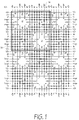
- the processor array which forms the embodiment of the invention is provided in an integrated circuit.
- the processor array is formed by a rectangular (and preferably square) array of "tiles" 10, one of which is shown bounded by a thick line in figure 1. Any appropriate number of tiles may be employed, for example in a 16 x 16, 32 x 32 or 64 x 64 array.
- Each tile 10 is rectangular (and preferably square) and is divided into four circuit areas. Two of the circuit areas 12, which are diagonally opposed in the tile 10, provide the locations for two arithmetic logic units (“ALUs"). The other two circuit areas, which are diagonally opposed in the tile 10, provide the locations for a pair of switching sections 14.
- ALUs arithmetic logic units
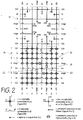
- each ALU has a first pair of 4-bit inputs a, which are directly connected within the ALU, a second pair of 4-bit inputs b, which are also directly connected within the ALU, and four 4-bit outputs f, which are directly connected within the ALU.
- Each ALU also has an independent pair of 1-bit carry inputs hci, vci, and a pair of 1-bit carry outputs co, which are directly connected within the ALU.
- the ALU can perform standard operations on the input signals a, b, hci, vci to produce the output signals f, co, such as add, subtract, AND, NAND, OR, NOR, XOR, NXOR and multiplexing and optionally can register the result of the operation.
- the instructions to the ALUs may be provided from respective 4-bit memory cells whose values can be set via the H-tree structure described below, or may be provided on the bus system which will be described below.
- a 4-gang programmable switch 16 is provided which can selectively connect the two busses at that crossing point.
- a 4-gang programmable switch 18 is provided which can selectively connect two busses which meet end to end at that crossing point, without any connection to the bus at right angles thereto.
- a programmable switch 20 (for example as shown in Figure 6C) is provided which can selectively connect the carry busses vc, hc which cross at right angles at that point.
- the busses h2s have a length of two tiles and are connectable end to end in every other switching section 14 by a programmable switch 18 at (4, 0).
- a bus hco extends from the carry output co of the ALU to the West to a programmable switch 20 at (4, 3), which can connect the bus hco (a) to a carry bus hci extending to the carry input hci of the ALU to the East or (b) to a carry bus vci extending to the carry input vci of the ALU to the South.
- the busses h1 have a length of one tile and are connectable end to end in each switching section 14 by a programmable switch 18 at (4, 5).
- the busses h2n have a length of two tiles and are connectable end to end in every other switching section 14 by a programmable switch 18 at (4, 7), staggered with respect to the programmable switches 18 connecting the busses h2s at (4, 0).
- the busses v2w have a length of two tiles and are connectable end to end in every other switching section 14 by a programmable switch 18 at (0, 3).
- the busses v1 have a length of one tile and are connectable end to end in each switching section 14 by a programmable switch 18 at (2, 3).
- a bus vco extends from the carry output co of the ALU to the North to the programmable switch 20 at (4, 3), which can connect the bus vco (a) to the carry bus hci extending to the carry input hci of the ALU to the East or (b) to the carry bus vci extending to the carry input vci of the ALU to the South.
- the busses v2e have a length of two tiles and are connectable end to end in every other switching section 14 by a programmable switch 18 at (7, 3) staggered with respect to the programmable switches 18 connecting the busses v2w at (0, 3).
- the busses bs, vco, fs are connected to input b, output co and output f, respectively, of the ALU to the North of the switching section 14.
- the busses fe, hco, be are connected to the output f, output co and input b of the ALU, respectively, to the West of the switching section 14.
- the busses aw, hci, fw are connected to the input a, input ci and output f, respectively, of the ALU to the East of the switching section 14.
- the busses fn, vci, an are connected to the output f, input ci and input a. respectively, of the ALU to the south of the switching section 14.
- busses vregw, vrege are connected via respective programmable switches 18 to 4-bit connection points vtsw, vtse, respectively, (shown by crosses in Figure 2) in the area 12 of the ALU to the North of the switching section 14.
- busses hregs, hregn are connected via respective programmable switches 18 to 4-bit connection points htse, htne, respectively, in the area 12 of the ALU to the West of the switching section 14.
- the busses hregs, hregn are connected via respective programmable switches 18 to 4-bit connection points htsw, htnw, respectively, in the area 12 of the ALU to the East of the switching section 14.
- busses vregw, vrege are connected via respective programmable switches 18 to 4-bit connection points vtnw, vtne, respectively, in the area 12 of the ALU to the south of the switching section 14.
- connection points vtnw, vtne, htne, htse, vtse, vtsw, htsw, htnw will be described below in further detail with reference to figures 3 to 5.
- busses hregn, vrege, hregs, vregw have respective 4-bit connection points 22 (shown by small squares in figure 2) which will be described below in further detail with reference to figure 9.
- Figure 3 shows one level of interconnections between the locations of the arithmetic logic units, which are illustrated by squares with rounded corners.
- a group of four 4-bit busses v8, v4w, v4e, v16 extend vertically across each column of ALU locations 12.
- the leftmost bus v8 in each group is in segments, each having a length generally of eight tiles.
- the leftmost but one bus v4w in each group is in segments, each having a length generally of four tiles.
- the rightmost but one bus v4e in each group is in segments, again each having a length generally of four tiles, but offset by two tiles from the leftmost but one bus v4w.
- the rightmost bus v16 in each group is in segments, each having a length generally of sixteen tiles.
- At the top edge of the array, which is at the top of figure 4, and at the bottom edge the lengths of the segments may be slightly greater than or shorter than specified above.
- each group of four busses v8, v4w, v4e, v16 crosses each ALU location 12
- four 4-bit tap connections are made at the connection points htnw, htsw, htse, htne.
- the ends of the bus segments take priority in being so connected over a connection to a bus segment which crosses the ALU location.
- a group of four 4-bit busses h8, h4n, h4s, h16 extend horizontally across each row of ALU locations 12.
- the uppermost bus h8 in each group is in segments, each having a length generally of eight tiles.
- the uppermost but one bus h4n in each group is in segments, each having a length generally of four tiles.
- the lowermost but one bus h4s in each group is in segments, again each having a length generally of four tiles, but offset by two tiles from the uppermost but one bus h4n.
- the lowermost bus h16 in each group is in segments, each having a length generally of sixteen tiles.
- each group of busses h8, h4n, h4s, h16 crosses each ALU location 12
- a further four 4-bit tap connections are made at the connection points vtnw, vtsw, vtse, vtne.
- the ends of the bus segments take priority in being so connected over a connection to a bus segment which crosses the ALU location.
- connection points htnw, htsw, htne, htse are connected via programmable switches to the busses hregn, hregs of the switching sections to the West and the East of the ALU location.
- connection points vtnw, vtne, vtsw, vtse are connected via programmable switches to the busses vregw, vrege of the switching sections to the North and the South of the ALU location.
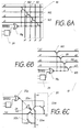
- the programmable connections 16 between pairs of 4-bit busses which cross at right angles will now be described with reference to figure 6A.
- the conductors of the horizontal busses are denoted as x0, x1, x2, x3, and the conductors of the vertical busses are denoted as y0, y1, y2, y3.
- a respective transistor 160, 161, 162, 163 is provided between each pair of conductors of the same bit significance.
- the gates of the transistors 160, 161, 162, 163 are connected in common to the output of a NOR gate 16g, which receives as its two inputs an inverted ENABLE signal from a single bit memory cell, which may be shared by a group of the switches, and the inverted content of a single bit memory cell 24.
- the conductors x0, x1, x2, x3 are connected by the transistors 160, 161, 162, 163, respectively, to the conductors y0, y1, y2, y3, respectively.
- the programmable connections 18 between pairs of 4-bit busses which meet each other end to end in line will now be described with reference to figure 6B.
- the conductors of one bus are denoted as x10, x11, x12, x13, and the conductors of the other bus are denoted as x20, x21, x22, x23.
- a respective transistor 180, 181, 182, 183 is provided between each pair of conductors of the same bit significance.
- the gates of the transistors 180, 181, 182, 183 are connected in common to the output of a NOR gate 18g, which receives as its two inputs an inverted ENABLE signal from a single bit memory cell, which may be shared by a group of the switches, and the inverted content of a single bit memory cell 24. Accordingly, only when the ENABLE signal is high and the content of the memory cell 24 is high, the conductors x10, x11, x12, x13 are connected by the transistors 180, 181, 182, 183, respectively, to the conductors x20, x21, x22, x23, respectively.
- the programmable connections 20 between the carry conductors hco,vco,hci,vci will now be described with reference to figure 6C.
- the horizontal carry output conductor hco is connected to the horizontal carry input conductor hci and the vertical carry input conductor vci via transistors 20hh, 20hv, respectively.
- the vertical carry output conductor vco is connected to the vertical carry input conductor vci and the horizontal carry input conductor hci via transistors 20vv, 20vh, respectively.
- the gates of the transistors 20hh, 20vv are connected in common to the output of an inverter 20i, and the gates of the transistors 20hv, 20vh and the input to the inverter 20i are connected to the output of a NOR gate 20g.
- the NOR gate 20g receives as its two inputs an inverted ENABLE signal from a single bit memory cell, which may be shared by a group of the switches, and the inverted content of a single bit memory cell 24. Accordingly, when the ENABLE signal is high, the conductors hco, vco are connected to the conductors hci, vci, respectively, or to the conductors vci, hci, respectively, in dependence upon the content of the memory cell 24.
- each of the switchable connections 16, 18, 20 described with reference to figures 6A to 6C includes a NOR gate 16g, 18g, 20g.
- NOR gate 16g is typically formed by four transistors 16g1, 16g2, 16g3, 16g4, two 16g1, 16g3 of which are responsive to the inverted ENABLE signal, and two 16g2, 16g4 of which are responsive to the inverted content of the memory cell 24.
- Such a group might consist of all of the switchable connections in one switching section 14, all of the switchable connections in the two switching sections 14 in a particular tile, or all of the switchable connections in a larger area of the array.
- the transistor 16g1 may be made common to all of the switchable connections 16, 18, 20 in the group, as shown in figure 8. This enabled a 25 % less one saving in the number of transistors required for the gates, but does require a further conductor linking the gate, as shown in figure 8.
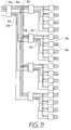
- busses hregn, hregs, vregw, vrege are connected by respective 4-bit connections 22 to a register or buffer circuit, and this circuit will now be described in more detail with reference to figure 9.
- the four connections 22 are each connected to respective inputs of a multiplexer 26.
- the multiplexer 26th selects one of the inputs as an output, which is supplied to a register or buffer 28.
- the output of the register or buffer 28 is supplied to four tri-state buffers 30s, 30w, 30n, 30e, which are connected back to the connections 22 to the busses hregs, vregw, hregn, vrege, respectively.
- the 4-bit signal on a selected one of the busses hregs, vregw, hregn, vrege is amplified and supplied to another selected one of the busses hregs, vregw, hregn, vrege.
- the 4-bit signal on a selected one of the busses hregs, vregw, hregn, vrege is amplified and supplied to any selected one of the busses hregs, vregw, hregn, vrege after the next active clock edge.
- these busses can be tapped part way along their lengths, so that the siting of the ALUs to perform a particular processing operation is not completely dictated by the lengths of the busses, and so that signals can be distributed to more than one ALU.
- the shorter length busses described with reference to figures 1 and 2 can be used to route signals between the switching sections 14 and the ALUs, and to send signals primarily over shorter distances, for example from one ALU to an adjacent ALU in the same row or column, or diagonally adjacent, even though the busses extend horizontally or vertically.
- the registers or buffers 28 can be used to amplify the signals or introduce programmable delays into them.
- the memory cells 24 are distributed across the array to the same extent as the switching actions 14 and the ALU locations 12.
- Each memory cell 24 is disposed adjacent the switch or switches, multiplexer, register or buffer which it controls. This enables a high circuit density be achieved.
- the decoder 34a determines which of the four branches from it leads to the address and supplies an ENABLE signal 30b to a further decoder 34b in that branch, together with a 4-bit address 32b to the decoders 34b in all four branches.
- the decoder 34b receiving the ENABLE signal 30b determines which of the four branches from it leads to the required address and supplies an ENABLE signal 30c to a further decoder 34c in that branch, together with a 4-bit address 32c to the decoders 34c in all four branches.
- the decoder 34c receiving the ENABLE signal 30c then supplies the ENABLE signal 34d to the required address where it can be stored in a single bit memory cell.
- a great advantage of the arrangement described above is that groups of the memory cells 24 in for example one switching section 14, or in the two switching sections in one tile, or in the switching sections in a sub-array of the tiles may be disabled en bloc by the inverted ENABLE signals so that the contents of those memory cells do not affect the associated switches. It is then possible for those memory cells 24 to be used as user memory by an application, rather than being used for configuring the wiring of the array.
- the embodiment of the invention has been described merely by way of example, and many modifications and developments may be made in keeping with the present invention.
- the embodiment employs ALUs as the processing units, but other processing units may additionally or alternatively be used, for example look-up tables, programmable logic arrays and/or self-contained CPUs which are able to fetch their own instructions.
- a sub-array might be composed of a 4 x 4 arrangement of tiles of ALUs and switching sections as described above, and the array might be composed of such sub-arrays and memory in a 4 x 4 array, or such sub-arrays and RISC CPUs in a 4 x 4 array.
- each ALU location is square, and each switching section is square and of the same size as the ALU locations, but it should be noted that the controllable switches 18 in the register busses vregw, vrege, hregn, hregs encroach into the square outline of the ALU locations.
- the ALU locations need not be of the same size as the switching sections, and in particular may be smaller, thus permitting one or more busses to pass horizontally or vertically directly from one switching section 14 to a diagonally adjacent switching section 14, for example running between the busses h2s, h2n or between the busses v2e, v2w.
- each ALU has two independent carry inputs vci, hci and a connected pair of carry outputs co.
- the ALUs may be arranged to deal with two types of carry: a fast carry between adjacent ALUs which may be of particular use for multi-bit adding operations; and a slow carry which can be routed more flexibly and may be of particular use for digital serial arithmetic.
- the fast carry might be arranged in a similar manner to that described above with reference to the drawings, whereas the slow carry might employ programmable switches in the switching sections 14 between the carry conductor and particular bits of the 4-bit busses.
- the array is two-dimensional, but the principles of the invention are also applicable to three-dimensional arrays, for example by providing a stack of the arrays described above, with the switching sections in adjacent layers staggered with respect to each other.
- the stack might include just two layers, but preferably at least three layers, and the number of layers is preferably a power of two.
- the memory cells 24 can be isolated by the gates 16g, 18g, 20g from the switches which they control so that the memory cells call be used for other purposes, that is put in the "user plane".
- the ENABLE signal memory cells cannot be transferred to the user plane.
- the switches in a particular switching section 14 may be disconnectable from the remainder of the array by further switches in the busses at the boundary of that switching section 14, with the further switches being controlled by a further memory cell which cannot be transferred to the user plane.
Abstract
A field programmable device comprises: an array of processing devices; a connection
matrix interconnecting the processing devices and including switches (160-163); and
memory cells (24) for storing data for controlling the switches to define the
configuration of the interconnections of the connection matrix.
In order to provide flexible use of memory and to enable higher memory densities, gates
(16g, 18g, 20g) are provided which can be used to isolate the effect of the data stored
in groups of the memory cells and switches on the configuration of the interconnections
so that the memory cells in that group are available for storing other data.
Description
This invention relates to a field programmable devices.
In particular, the invention relates to such a device comprising: a plurality of processing
devices: a connection matrix interconnecting the processing devices and including a
plurality of switches; a plurality of memory cells for storing data for controlling the
switches to define the configuration of the interconnections of the connection matrix.
The problems with which the present invention (or at least preferred embodiments of it)
is concerned are to provide more flexible use of memory, to enable higher memory
density and higher circuit density.
In accordance with a first aspect of the present invention, there is provided means for
isolating the effect of the data stored in at least one group of the memory cells and
switches on the configuration of the interconnections so that the memory cells in that
group are available for storing other data. Accordingly, the memory cells can be
selectively used (a) for controlling the interconnections and (b) as user memory. By
providing this feature using the configuration memory for the switches, higher memory
density can be achieved.
In one embodiment, the isolating means comprises means for isolating each of the
memory cells in the group from the switches. This enables isolation without requiring
additional switches to be introduced into the wiring of the connection matrix, which
would increase signal propagation delay and so reduce circuit speed.
This latter feature may be provided in devices which do not require memory cells to be
isolated in groups. Therefore, in accordance with a second aspect of the present
invention, there is provided a field programmable device, comprising: a plurality of
processing devices; a connection matrix interconnecting the processing devices and
including a plurality of switches: a plurality of memory cells for storing data for
controlling the switches to define the configuration of the interconnections of the
connection matrix; and means for isolating each of the memory cells from the switch or
switches controllable by that memory cell.
The isolating means is preferably operable to set each of the switches in the group to a
predetermined state upon isolation from the respective memory cell. Accordingly, when
isolated, the switches may still provide a predetermined connection in the connection
matrix, but they may all he set to  off
off .
.
The isolating means preferably comprises, for each memory cell, a respective gate
having inputs connected to the memory cell and to a control signal, and having an output
connected to the or each switch which can be controlled by that memory cell. The use
of a gate ensures that the switch is controlled by a well defined logic level at all times,
whether it is being controlled by the memory cell or the control signal. Each gate may
provided by four transistors, and one of the transistors of each gate may be common to
a plurality of the gates, thus enabling an increased circuit density to be achieved.
In another embodiment, the isolating means comprises means for isolating each of the
switches in the group from the remainder of the connection matrix.
At least some of the interconnections provided by the connection matrix may be in the
form of plural-bit busses, with those of the switches for the busses each comprising a
plurality of switch elements each for a respective bit of the bus.
The positions of the memory cells are preferably distributed across the device to
substantially the same extent as the switches, and each of the memory cells is disposed
adjacent the switch or switches controllable by that memory cell, thus enabling a high
circuit density to be achieved.
This latter feature may be provided, whether or not the memory cells are isolatable.
Therefore, in accordance with a third aspect of the present invention, there is provided
a field programmable device, comprising; a plurality of processing devices; a connection
matrix interconnecting the processing devices and including a plurality of switches; and
a plurality of memory cells for storing data for controlling the switches to define the
configuration of the interconnections of the connection matrix; wherein the positions of
the memory cells are distributed across the device to substantially the same extent as the
switches, and each of the memory cells is disposed adjacent the switch or switches
controllable by that memory cell.
A specific embodiment of the present invention will now be described, by way of
example, with reference to the accompanying drawings, in which:
In the following, description, the terms "horizontal", "vertical", "North", "South",
"East" and "West" have been used to assist in an understanding of relative directions,
but their use is not intended to imply any restriction on the absolute orientation of the
embodiment of the invention.
The processor array which forms the embodiment of the invention is provided in an
integrated circuit. At one level, the processor array is formed by a rectangular (and
preferably square) array of "tiles" 10, one of which is shown bounded by a thick line
in figure 1. Any appropriate number of tiles may be employed, for example in a 16 x
16, 32 x 32 or 64 x 64 array. Each tile 10 is rectangular (and preferably square) and is
divided into four circuit areas. Two of the circuit areas 12, which are diagonally
opposed in the tile 10, provide the locations for two arithmetic logic units ("ALUs").
The other two circuit areas, which are diagonally opposed in the tile 10, provide the
locations for a pair of switching sections 14.
Referring to figures 1 and 2, each ALU has a first pair of 4-bit inputs a, which are
directly connected within the ALU, a second pair of 4-bit inputs b, which are also
directly connected within the ALU, and four 4-bit outputs f, which are directly
connected within the ALU. Each ALU also has an independent pair of 1-bit carry inputs
hci, vci, and a pair of 1-bit carry outputs co, which are directly connected within the
ALU. The ALU can perform standard operations on the input signals a, b, hci, vci to
produce the output signals f, co, such as add, subtract, AND, NAND, OR, NOR, XOR,
NXOR and multiplexing and optionally can register the result of the operation. The
instructions to the ALUs may be provided from respective 4-bit memory cells whose
values can be set via the H-tree structure described below, or may be provided on the
bus system which will be described below.
At the level shown in figures 1 and 2, each switching section 14 has eight busses
extending across it horizontally, and eight busses extending across it vertically, thus
forming an 8 x 8 rectangular array of 64 crossing points, which have been numbered in
figure 2 with Cartesian co-ordinates. All of the busses have a width of four bits, with
the exception of the carry bus vc at X = 4 and the carry bus hc at Y = 3, which have a
width of one bit. At many of the crossing points, a 4-gang programmable switch 16 is
provided which can selectively connect the two busses at that crossing point. At some
of the crossing points, a 4-gang programmable switch 18 is provided which can
selectively connect two busses which meet end to end at that crossing point, without any
connection to the bus at right angles thereto. At the crossing point at (4, 3), a
programmable switch 20 (for example as shown in Figure 6C) is provided which can
selectively connect the carry busses vc, hc which cross at right angles at that point.
The horizontal busses in the switching section 14 will now be described.
At Y = 0, busses h2s are connectable by programmable switches 16 to the vertical busses
at X = 0, 1, 2, 5, 6. The busses h2s have a length of two tiles and are connectable end
to end in every other switching section 14 by a programmable switch 18 at (4, 0).
At Y = 1, a bus bc extending from an input b of the ALU to the West is connectable by
switches 16 to the vertical busses at X = 0, 1, 2, 3. Also, a bus fw extending from an
output f of the ALU to the East is connectable by switches 16 to the vertical busses at
X = 5, 6, 7. The ends of the busses be, fw are connectable by a programmable switch
18 at (4, 1).
At Y = 2, a bus hregs is connectable by programmable switches 16 to the vertical busses
at X = 1, 2, 3, 5, 6, 7.
At Y = 3, a bus hco extends from the carry output co of the ALU to the West to a
programmable switch 20 at (4, 3), which can connect the bus hco (a) to a carry bus hci
extending to the carry input hci of the ALU to the East or (b) to a carry bus vci
extending to the carry input vci of the ALU to the South.
At Y = 4, a bus hregn is connectable by programmable switches 16 to the vertical busses
at X = 0, 1, 2, 3, 5, 6.
At Y = 5, busses h1 are connectable to the vertical busses at X = 0, 1, 2, 3, 5, 6, 7. The
busses h1 have a length of one tile and are connectable end to end in each switching
section 14 by a programmable switch 18 at (4, 5).
At Y = 6, a bus fe extending from an output f of the ALU to the West is connectable by
switches 16 to the vertical busses at X = 0, 1, 2, 3. Also, a bus aw extending from an
input a of the ALU to the East is connectable by switches 16 to the vertical busses at
X = 5, 6, 7. The ends of the busses fe, aw are connectable by a programmable switch 18
at (4, 6).
At Y = 7, busses h2n are connectable by programmable switches 16 to the vertical busses
at X = 1, 2, 3, 6, 7. The busses h2n have a length of two tiles and are connectable end
to end in every other switching section 14 by a programmable switch 18 at (4, 7),
staggered with respect to the programmable switches 18 connecting the busses h2s at (4,
0).
The vertical busses in the switching section 14 will now be described.
At X = 0, busses v2w are connectable by programmable switches 16 to the horizontal
busses at Y = 0, 1, 4, 5, 6. The busses v2w have a length of two tiles and are
connectable end to end in every other switching section 14 by a programmable switch
18 at (0, 3).
At X = 1, a bus fn extending from an output f of the ALU to the South is connectable by
programmable switches 16 to the horizontal busses at Y = 0, 1, 2. Also, a bus bs
extending from an input b of the ALU to the North is connectable by switches 16 to the
horizontal busses at Y = 4, 5, 6, 7. The ends of the busses fn, bs are connectable by a
programmable switch 18 at (1, 3).
At X = 2, busses v1 are connectable to the horizontal busses at Y = 0, 1, 2, 4, 5, 6, 7.
The busses v1 have a length of one tile and are connectable end to end in each switching
section 14 by a programmable switch 18 at (2, 3).
At X = 3, a bus vregw is connectable by programmable switches 16 to the horizontal
busses at Y = 1, 2, 4, 5, 6, 7.
At X = 4, a bus vco extends from the carry output co of the ALU to the North to the
programmable switch 20 at (4, 3), which can connect the bus vco (a) to the carry bus
hci extending to the carry input hci of the ALU to the East or (b) to the carry bus vci
extending to the carry input vci of the ALU to the South.
At X = 5, a bus vregc is connectable by programmable switches 16 to the horizontal
busses at Y = 0, 1, 2, 4, 5, 6.
At X = 6. a bus an extending from an input a of the ALU to the South is connectable by
switches 16 to the horizontal busses at Y = 0, 1, 2. Also, a bus fs extending from an
output f of the ALU to the North is connectable by programmable switches 16 to the
horizontal busses at Y = 4, 5, 6, 7. The ends of the busses an, fs are connectable by a
programmable switch 18 at (6, 3).
At X = 7, busses v2e are connectable by programmable switches 16 to the horizontal
busses at Y = 1, 2, 5, 6, 7. The busses v2e have a length of two tiles and are connectable
end to end in every other switching section 14 by a programmable switch 18 at (7, 3)
staggered with respect to the programmable switches 18 connecting the busses v2w at
(0, 3).
As shown in figure 2, the busses bs, vco, fs are connected to input b, output co and
output f, respectively, of the ALU to the North of the switching section 14. Also, the
busses fe, hco, be are connected to the output f, output co and input b of the ALU,
respectively, to the West of the switching section 14. Furthermore, the busses aw, hci,
fw are connected to the input a, input ci and output f, respectively, of the ALU to the
East of the switching section 14. Moreover, the busses fn, vci, an are connected to the
output f, input ci and input a. respectively, of the ALU to the south of the switching
section 14.
In addition to these connections, the busses vregw, vrege are connected via respective
programmable switches 18 to 4-bit connection points vtsw, vtse, respectively, (shown
by crosses in Figure 2) in the area 12 of the ALU to the North of the switching section
14. Also, the busses hregs, hregn are connected via respective programmable switches
18 to 4-bit connection points htse, htne, respectively, in the area 12 of the ALU to the
West of the switching section 14. Furthermore, the busses hregs, hregn are connected
via respective programmable switches 18 to 4-bit connection points htsw, htnw,
respectively, in the area 12 of the ALU to the East of the switching section 14.
Moreover, the busses vregw, vrege are connected via respective programmable switches
18 to 4-bit connection points vtnw, vtne, respectively, in the area 12 of the ALU to the
south of the switching section 14. These connection points vtnw, vtne, htne, htse, vtse,
vtsw, htsw, htnw will be described below in further detail with reference to figures 3
to 5.
Also, as shown in figure 2, the busses hregn, vrege, hregs, vregw have respective 4-bit
connection points 22 (shown by small squares in figure 2) which will be described below
in further detail with reference to figure 9.
Figure 3 shows one level of interconnections between the locations of the arithmetic
logic units, which are illustrated by squares with rounded corners. A group of four 4-bit
busses v8, v4w, v4e, v16 extend vertically across each column of ALU locations 12.
The leftmost bus v8 in each group is in segments, each having a length generally of eight
tiles. The leftmost but one bus v4w in each group is in segments, each having a length
generally of four tiles. The rightmost but one bus v4e in each group is in segments,
again each having a length generally of four tiles, but offset by two tiles from the
leftmost but one bus v4w. The rightmost bus v16 in each group is in segments, each
having a length generally of sixteen tiles. At the top edge of the array, which is at the
top of figure 4, and at the bottom edge the lengths of the segments may be slightly
greater than or shorter than specified above.
Referring to figures 3 and 5, where each group of four busses v8, v4w, v4e, v16 crosses
each ALU location 12, four 4-bit tap connections are made at the connection points
htnw, htsw, htse, htne. The ends of the bus segments take priority in being so connected
over a connection to a bus segment which crosses the ALU location.
Similarly, as shown in figures 4 and 5, a group of four 4-bit busses h8, h4n, h4s, h16
extend horizontally across each row of ALU locations 12. The uppermost bus h8 in each
group is in segments, each having a length generally of eight tiles. The uppermost but
one bus h4n in each group is in segments, each having a length generally of four tiles.
The lowermost but one bus h4s in each group is in segments, again each having a length
generally of four tiles, but offset by two tiles from the uppermost but one bus h4n. The
lowermost bus h16 in each group is in segments, each having a length generally of
sixteen tiles. At the left hand edge of the array, which is at the left of figure 4, and at
the right hand edge the length of the segments may be slightly greater than or shorter
than specified above. Where each group of busses h8, h4n, h4s, h16 crosses each ALU
location 12, a further four 4-bit tap connections are made at the connection points vtnw,
vtsw, vtse, vtne. The ends of the bus segments take priority in being so connected over
a connection to a bus segment which crosses the ALU location.
As shown in figure 5, the connection points htnw, htsw, htne, htse are connected via
programmable switches to the busses hregn, hregs of the switching sections to the West
and the East of the ALU location. Also, the connection points vtnw, vtne, vtsw, vtse are
connected via programmable switches to the busses vregw, vrege of the switching
sections to the North and the South of the ALU location.
The programmable connections 16 between pairs of 4-bit busses which cross at right
angles will now be described with reference to figure 6A. The conductors of the
horizontal busses are denoted as x0, x1, x2, x3, and the conductors of the vertical busses
are denoted as y0, y1, y2, y3. Between each pair of conductors of the same bit
significance, a respective transistor 160, 161, 162, 163 is provided. The gates of the
transistors 160, 161, 162, 163 are connected in common to the output of a NOR gate
16g, which receives as its two inputs an inverted ENABLE signal from a single bit
memory cell, which may be shared by a group of the switches, and the inverted content
of a single bit memory cell 24. Accordingly, only when the ENABLE signal is high and
the content of the memory cell 24 is high, the conductors x0, x1, x2, x3 are connected
by the transistors 160, 161, 162, 163, respectively, to the conductors y0, y1, y2, y3,
respectively.
The programmable connections 18 between pairs of 4-bit busses which meet each other
end to end in line will now be described with reference to figure 6B. The conductors of
one bus are denoted as x10, x11, x12, x13, and the conductors of the other bus are
denoted as x20, x21, x22, x23. Between each pair of conductors of the same bit
significance, a respective transistor 180, 181, 182, 183 is provided. The gates of the
transistors 180, 181, 182, 183 are connected in common to the output of a NOR gate
18g, which receives as its two inputs an inverted ENABLE signal from a single bit
memory cell, which may be shared by a group of the switches, and the inverted content
of a single bit memory cell 24. Accordingly, only when the ENABLE signal is high and
the content of the memory cell 24 is high, the conductors x10, x11, x12, x13 are
connected by the transistors 180, 181, 182, 183, respectively, to the conductors x20,
x21, x22, x23, respectively.
The programmable connections 20 between the carry conductors hco,vco,hci,vci will
now be described with reference to figure 6C. The horizontal carry output conductor hco
is connected to the horizontal carry input conductor hci and the vertical carry input
conductor vci via transistors 20hh, 20hv, respectively. Furthermore, the vertical carry
output conductor vco is connected to the vertical carry input conductor vci and the
horizontal carry input conductor hci via transistors 20vv, 20vh, respectively. The gates
of the transistors 20hh, 20vv are connected in common to the output of an inverter 20i,
and the gates of the transistors 20hv, 20vh and the input to the inverter 20i are connected
to the output of a NOR gate 20g. The NOR gate 20g receives as its two inputs an
inverted ENABLE signal from a single bit memory cell, which may be shared by a
group of the switches, and the inverted content of a single bit memory cell 24.
Accordingly, when the ENABLE signal is high, the conductors hco, vco are connected
to the conductors hci, vci, respectively, or to the conductors vci, hci, respectively, in
dependence upon the content of the memory cell 24.
It will be noted that each of the switchable connections 16, 18, 20 described with
reference to figures 6A to 6C includes a NOR gate 16g, 18g, 20g. As shown in figure
7, a NOR gate 16g is typically formed by four transistors 16g1, 16g2, 16g3, 16g4, two
16g1, 16g3 of which are responsive to the inverted ENABLE signal, and two 16g2,
16g4 of which are responsive to the inverted content of the memory cell 24. In the
embodiment of the invention, it is desirable that a group of the switchable collections 16,
18, 20 may be disabled in common, without any need for only part of such a group to
be disabled. Such a group might consist of all of the switchable connections in one
switching section 14, all of the switchable connections in the two switching sections 14
in a particular tile, or all of the switchable connections in a larger area of the array. In
this case, the transistor 16g1 may be made common to all of the switchable connections
16, 18, 20 in the group, as shown in figure 8. This enabled a 25 % less one saving in the
number of transistors required for the gates, but does require a further conductor linking
the gate, as shown in figure 8.
As mentioned above with reference to figures 1 and 2, at each switching section 14, the
busses hregn, hregs, vregw, vrege are connected by respective 4-bit connections 22 to
a register or buffer circuit, and this circuit will now be described in more detail with
reference to figure 9. The four connections 22 are each connected to respective inputs
of a multiplexer 26. The multiplexer 26th selects one of the inputs as an output, which
is supplied to a register or buffer 28. The output of the register or buffer 28 is supplied
to four tri-state buffers 30s, 30w, 30n, 30e, which are connected back to the connections
22 to the busses hregs, vregw, hregn, vrege, respectively. In the ease where a buffer 28
is used, the 4-bit signal on a selected one of the busses hregs, vregw, hregn, vrege is
amplified and supplied to another selected one of the busses hregs, vregw, hregn, vrege.
In the case where a register 28 is used, the 4-bit signal on a selected one of the busses
hregs, vregw, hregn, vrege is amplified and supplied to any selected one of the busses
hregs, vregw, hregn, vrege after the next active clock edge.
It will be appreciated that the arrangement described above provides great flexibility in
the routing of signals around and across the array. With appropriate setting of the
switches 16, 18, 20 using tile memory cells 24 and with appropriate setting of the
multiplexers 26 and registers or buffers 28, signals can been sent over large distances,
primarily using the busses v16, h16, v8, h8, v4e, v4w, h4n, h4s from the edge of the
array to a particular ALU, between ALUs, and from a particular ALU to the edge of
the array. These busses can be joined together in line, or at right angles, by the
switching sections 14, with amplification by the registers or buffers 28 in order to
reduce propagation delays, and with pipeline stages introduced by the registers 28. Also,
these busses can be tapped part way along their lengths, so that the siting of the ALUs
to perform a particular processing operation is not completely dictated by the lengths of
the busses, and so that signals can be distributed to more than one ALU. Furthermore,
the shorter length busses described with reference to figures 1 and 2 can be used to route
signals between the switching sections 14 and the ALUs, and to send signals primarily
over shorter distances, for example from one ALU to an adjacent ALU in the same row
or column, or diagonally adjacent, even though the busses extend horizontally or
vertically. Again, the registers or buffers 28 can be used to amplify the signals or
introduce programmable delays into them.
In the arrangement described above, the memory cells 24 are distributed across the array
to the same extent as the switching actions 14 and the ALU locations 12. Each memory
cell 24 is disposed adjacent the switch or switches, multiplexer, register or buffer which
it controls. This enables a high circuit density be achieved.
A description will now be made of the manner in which data is written to or read from
the memory cells 24, the way in which the ENABLE signals for the programmable
switches 16, 18, 20 are written to their memory cells, the way in which instructions, and
possibly constants, are distributed to the ALUs, and the way in which other control
signals, such as a clock signal, are transmitted across the array. For all of these
functions, an "H-tree" structure (which is known per se) may be employed, as shown
in figure 10. Referring to Figures 10 and 11, in order to distribute an ENABLE signal
to any of 64 locations in the example shown, the ENABLE signal 30a and a 6-bit address
32a for it are supplied to a decoder 34a. The decoder 34a determines which of the four
branches from it leads to the address and supplies an ENABLE signal 30b to a further
decoder 34b in that branch, together with a 4-bit address 32b to the decoders 34b in all
four branches. The decoder 34b receiving the ENABLE signal 30b determines which of
the four branches from it leads to the required address and supplies an ENABLE signal
30c to a further decoder 34c in that branch, together with a 4-bit address 32c to the
decoders 34c in all four branches. The decoder 34c receiving the ENABLE signal 30c
then supplies the ENABLE signal 34d to the required address where it can be stored in
a single bit memory cell. An advantage of the H-tree structure is that the lengths of the
signal paths to all of the destinations are approximately equal, which is particularly
advantageous in the case of the clock signal.
A great advantage of the arrangement described above is that groups of the memory cells
24 in for example one switching section 14, or in the two switching sections in one tile,
or in the switching sections in a sub-array of the tiles may be disabled en bloc by the
inverted ENABLE signals so that the contents of those memory cells do not affect the
associated switches. It is then possible for those memory cells 24 to be used as user
memory by an application, rather than being used for configuring the wiring of the
array.
The embodiment of the invention has been described merely by way of example, and
many modifications and developments may be made in keeping with the present
invention. For example, the embodiment employs ALUs as the processing units, but
other processing units may additionally or alternatively be used, for example look-up
tables, programmable logic arrays and/or self-contained CPUs which are able to fetch
their own instructions.
Furthermore, the embodiment has been described as if the whole array is covered by
ALUs and switching sections. However, other types of section may be included in the
array. For example, a sub-array might be composed of a 4 x 4 arrangement of tiles of
ALUs and switching sections as described above, and the array might be composed of
such sub-arrays and memory in a 4 x 4 array, or such sub-arrays and RISC CPUs in a
4 x 4 array.
In the embodiment described above, each ALU location is square, and each switching
section is square and of the same size as the ALU locations, but it should be noted that
the controllable switches 18 in the register busses vregw, vrege, hregn, hregs encroach
into the square outline of the ALU locations. The ALU locations need not be of the same
size as the switching sections, and in particular may be smaller, thus permitting one or
more busses to pass horizontally or vertically directly from one switching section 14 to
a diagonally adjacent switching section 14, for example running between the busses h2s,
h2n or between the busses v2e, v2w.
In the embodiment described above, each ALU has two independent carry inputs vci,
hci and a connected pair of carry outputs co. If required, the ALUs may be arranged to
deal with two types of carry: a fast carry between adjacent ALUs which may be of
particular use for multi-bit adding operations; and a slow carry which can be routed
more flexibly and may be of particular use for digital serial arithmetic. The fast carry
might be arranged in a similar manner to that described above with reference to the
drawings, whereas the slow carry might employ programmable switches in the switching
sections 14 between the carry conductor and particular bits of the 4-bit busses.
In the embodiment described above, particular bit widths, sizes of switching section and
sizes of array have been mentioned, but it should be noted that all of these values may
be changed as appropriate. Also, the programmable switches 16, 18, 20 have been
described as being disposed at particular locations in each switching section 14, but other
locations may be used as required and desired.
In the embodiment described above, the array is two-dimensional, but the principles of
the invention are also applicable to three-dimensional arrays, for example by providing
a stack of the arrays described above, with the switching sections in adjacent layers
staggered with respect to each other. The stack might include just two layers, but
preferably at least three layers, and the number of layers is preferably a power of two.
In the embodiment described above, the memory cells 24 can be isolated by the gates
16g, 18g, 20g from the switches which they control so that the memory cells call be
used for other purposes, that is put in the "user plane". The ENABLE signal memory
cells, however, cannot be transferred to the user plane. In an alternative embodiment,
the switches in a particular switching section 14 may be disconnectable from the
remainder of the array by further switches in the busses at the boundary of that
switching section 14, with the further switches being controlled by a further memory cell
which cannot be transferred to the user plane.
Many other modifications and developments may also be made.
Claims (10)
- A field programmable device, comprising:a plurality of processing devices;a connection matrix (14) interconnecting the processing devices and including a plurality of switches (16, 18, 20);a plurality of memory cells (24) for storing data for controlling the switches to define the configuration of the interconnections of the connection matrix; andmeans (16g, 18g, 20g) for isolating the effect of the data stored in at least one group of the memory cells and switches on the configuration of the interconnections so that the memory cells in that group are available for storing other data.
- A device as claimed in claim 1, wherein the isolating means comprises means (16g, 18g, 20g) for isolating each of the memory cells in the group from the switches.
- A field programmable device, comprising:a plurality of processing devices;a connection matrix (14) interconnecting the processing devices and including a plurality of switches (16, 18, 20);a plurality of memory cells (24) for storing data for controlling the switches to define the configuration of the interconnections of the connection matrix; andmeans (16g, 18g, 20g) for isolating each of the memory cells from the switch or switches controllable by that memory cell.
- A device as claimed in claim 2 or 3, wherein the isolating means is operable to set each of the switches in the group to a predetermined state upon isolation from the respective memory cell.
- A device as claimed in any of claims 2 to 4, wherein the isolating means comprises, for each memory cell, a respective gate (16g, 18g, 20g) having inputs connected to the memory cell and to a control signal (ENABLE), and having an output connected to the or each switch which can be controlled by that memory cell.
- A device as claimed in claim 5, wherein each gate is provided by four transistors (16g1-16g4).
- A device as claimed in claim 6, wherein one of the transistors (16g1) of each gate is common to a plurality of the gates.
- A device as claimed in claim 1, wherein the isolating means comprises means for isolating each of the switches in the group from the remainder of the connection matrix.
- A device as claimed in any preceding claim, wherein at least some of the interconnections provided by the connection matrix are in the form of plural-bit busses; and those of the switches for the busses each comprise a plurality of switch elements (160-163, 180-183) each for a respective bit of the bus.
- A device as claimed in any preceding claim, wherein the positions of the memory cells are distributed across the device to substantially the same extent as the switches, and each of the memory cells is disposed adjacent the switch or switches controllable by that memory cell.
Priority Applications (7)
| Application Number | Priority Date | Filing Date | Title |
|---|---|---|---|
| EP97300562A EP0858167A1 (en) | 1997-01-29 | 1997-01-29 | Field programmable processor device |
| US09/341,565 US6262908B1 (en) | 1997-01-29 | 1998-01-28 | Field programmable processor devices |
| PCT/GB1998/000248 WO1998033276A1 (en) | 1997-01-29 | 1998-01-28 | Field programmable processor |
| EP98901401A EP0956645B1 (en) | 1997-01-29 | 1998-01-28 | Field programmable processor |
| JP53175598A JP3885119B2 (en) | 1997-01-29 | 1998-01-28 | Field programmable processor device |
| DE69822796T DE69822796T2 (en) | 1997-01-29 | 1998-01-28 | USER PROGRAMMABLE PROCESSOR |
| US09/891,847 US20010038298A1 (en) | 1997-01-29 | 2001-06-25 | Field programmable processor devices |
Applications Claiming Priority (1)
| Application Number | Priority Date | Filing Date | Title |
|---|---|---|---|
| EP97300562A EP0858167A1 (en) | 1997-01-29 | 1997-01-29 | Field programmable processor device |
Publications (1)
| Publication Number | Publication Date |
|---|---|
| EP0858167A1 true EP0858167A1 (en) | 1998-08-12 |
Family
ID=8229198
Family Applications (2)
| Application Number | Title | Priority Date | Filing Date |
|---|---|---|---|
| EP97300562A Withdrawn EP0858167A1 (en) | 1997-01-29 | 1997-01-29 | Field programmable processor device |
| EP98901401A Expired - Lifetime EP0956645B1 (en) | 1997-01-29 | 1998-01-28 | Field programmable processor |
Family Applications After (1)
| Application Number | Title | Priority Date | Filing Date |
|---|---|---|---|
| EP98901401A Expired - Lifetime EP0956645B1 (en) | 1997-01-29 | 1998-01-28 | Field programmable processor |
Country Status (5)
| Country | Link |
|---|---|
| US (2) | US6262908B1 (en) |
| EP (2) | EP0858167A1 (en) |
| JP (1) | JP3885119B2 (en) |
| DE (1) | DE69822796T2 (en) |
| WO (1) | WO1998033276A1 (en) |
Cited By (2)
| Publication number | Priority date | Publication date | Assignee | Title |
|---|---|---|---|---|
| US7219325B1 (en) * | 2003-11-21 | 2007-05-15 | Xilinx, Inc. | Exploiting unused configuration memory cells |
| CN101743692B (en) * | 2007-06-20 | 2016-08-03 | 雅格罗技公司 | A kind of programmable interconnection network for logic array |
Families Citing this family (34)
| Publication number | Priority date | Publication date | Assignee | Title |
|---|---|---|---|---|
| US7266725B2 (en) | 2001-09-03 | 2007-09-04 | Pact Xpp Technologies Ag | Method for debugging reconfigurable architectures |
| DE19651075A1 (en) | 1996-12-09 | 1998-06-10 | Pact Inf Tech Gmbh | Unit for processing numerical and logical operations, for use in processors (CPU's), multi-computer systems, data flow processors (DFP's), digital signal processors (DSP's) or the like |
| DE19654595A1 (en) | 1996-12-20 | 1998-07-02 | Pact Inf Tech Gmbh | I0 and memory bus system for DFPs as well as building blocks with two- or multi-dimensional programmable cell structures |
| ATE243390T1 (en) | 1996-12-27 | 2003-07-15 | Pact Inf Tech Gmbh | METHOD FOR INDEPENDENT DYNAMIC LOADING OF DATA FLOW PROCESSORS (DFPS) AND COMPONENTS WITH TWO- OR MULTI-DIMENSIONAL PROGRAMMABLE CELL STRUCTURES (FPGAS, DPGAS, O.L.) |
| US6542998B1 (en) | 1997-02-08 | 2003-04-01 | Pact Gmbh | Method of self-synchronization of configurable elements of a programmable module |
| US8686549B2 (en) | 2001-09-03 | 2014-04-01 | Martin Vorbach | Reconfigurable elements |
| DE19861088A1 (en) | 1997-12-22 | 2000-02-10 | Pact Inf Tech Gmbh | Repairing integrated circuits by replacing subassemblies with substitutes |
| AU5805300A (en) | 1999-06-10 | 2001-01-02 | Pact Informationstechnologie Gmbh | Sequence partitioning in cell structures |
| EP1061439A1 (en) | 1999-06-15 | 2000-12-20 | Hewlett-Packard Company | Memory and instructions in computer architecture containing processor and coprocessor |
| EP1342158B1 (en) | 2000-06-13 | 2010-08-04 | Richter, Thomas | Pipeline configuration unit protocols and communication |
| US7383424B1 (en) | 2000-06-15 | 2008-06-03 | Hewlett-Packard Development Company, L.P. | Computer architecture containing processor and decoupled coprocessor |
| US8058899B2 (en) | 2000-10-06 | 2011-11-15 | Martin Vorbach | Logic cell array and bus system |
| US9037807B2 (en) | 2001-03-05 | 2015-05-19 | Pact Xpp Technologies Ag | Processor arrangement on a chip including data processing, memory, and interface elements |
| US7844796B2 (en) | 2001-03-05 | 2010-11-30 | Martin Vorbach | Data processing device and method |
| US7444531B2 (en) | 2001-03-05 | 2008-10-28 | Pact Xpp Technologies Ag | Methods and devices for treating and processing data |
| US7581076B2 (en) * | 2001-03-05 | 2009-08-25 | Pact Xpp Technologies Ag | Methods and devices for treating and/or processing data |
| US7657877B2 (en) * | 2001-06-20 | 2010-02-02 | Pact Xpp Technologies Ag | Method for processing data |
| US7996827B2 (en) | 2001-08-16 | 2011-08-09 | Martin Vorbach | Method for the translation of programs for reconfigurable architectures |
| US7434191B2 (en) | 2001-09-03 | 2008-10-07 | Pact Xpp Technologies Ag | Router |
| US8686475B2 (en) | 2001-09-19 | 2014-04-01 | Pact Xpp Technologies Ag | Reconfigurable elements |
| EP1483682A2 (en) | 2002-01-19 | 2004-12-08 | PACT XPP Technologies AG | Reconfigurable processor |
| EP2043000B1 (en) | 2002-02-18 | 2011-12-21 | Richter, Thomas | Bus systems and reconfiguration method |
| US8914590B2 (en) | 2002-08-07 | 2014-12-16 | Pact Xpp Technologies Ag | Data processing method and device |
| US6844757B2 (en) | 2002-06-28 | 2005-01-18 | Lattice Semiconductor Corp. | Converting bits to vectors in a programmable logic device |
| AU2003286131A1 (en) | 2002-08-07 | 2004-03-19 | Pact Xpp Technologies Ag | Method and device for processing data |
| US7657861B2 (en) | 2002-08-07 | 2010-02-02 | Pact Xpp Technologies Ag | Method and device for processing data |
| JP4388895B2 (en) | 2002-09-06 | 2009-12-24 | ペーアーツェーテー イクスペーペー テクノロジーズ アクチエンゲゼルシャフト | Reconfigurable sequencer structure |
| US6980390B2 (en) * | 2003-02-05 | 2005-12-27 | Quantum Corporation | Magnetic media with embedded optical servo tracks |
| EP1676208A2 (en) | 2003-08-28 | 2006-07-05 | PACT XPP Technologies AG | Data processing device and method |
| US7853774B1 (en) * | 2005-03-25 | 2010-12-14 | Tilera Corporation | Managing buffer storage in a parallel processing environment |
| EP1974265A1 (en) | 2006-01-18 | 2008-10-01 | PACT XPP Technologies AG | Hardware definition method |
| WO2008028330A1 (en) * | 2006-08-31 | 2008-03-13 | Beijing Xizheng Microelectronics Co. Ltd. | A programmable interconnect network for logic array |
| JP5336398B2 (en) | 2010-02-01 | 2013-11-06 | ルネサスエレクトロニクス株式会社 | Semiconductor integrated circuit and semiconductor integrated circuit configuration changing method |
| US9557154B2 (en) | 2010-05-25 | 2017-01-31 | The General Hospital Corporation | Systems, devices, methods, apparatus and computer-accessible media for providing optical imaging of structures and compositions |
Citations (2)
| Publication number | Priority date | Publication date | Assignee | Title |
|---|---|---|---|---|
| US5426379A (en) * | 1994-07-29 | 1995-06-20 | Xilinx, Inc. | Field programmable gate array with built-in bitstream data expansion |
| US5583450A (en) * | 1995-08-18 | 1996-12-10 | Xilinx, Inc. | Sequencer for a time multiplexed programmable logic device |
Family Cites Families (12)
| Publication number | Priority date | Publication date | Assignee | Title |
|---|---|---|---|---|
| US4236204A (en) | 1978-03-13 | 1980-11-25 | Motorola, Inc. | Instruction set modifier register |
| US5233539A (en) | 1989-08-15 | 1993-08-03 | Advanced Micro Devices, Inc. | Programmable gate array with improved interconnect structure, input/output structure and configurable logic block |
| US5204556A (en) | 1991-05-06 | 1993-04-20 | Lattice Semiconductor Corporation | Programmable interconnect structure for logic blocks |
| US5291431A (en) | 1991-06-03 | 1994-03-01 | General Electric Company | Array multiplier adapted for tiled layout by silicon compiler |
| US5208491A (en) | 1992-01-07 | 1993-05-04 | Washington Research Foundation | Field programmable gate array |
| US5498975A (en) * | 1992-11-19 | 1996-03-12 | Altera Corporation | Implementation of redundancy on a programmable logic device |
| WO1995022205A1 (en) | 1994-02-15 | 1995-08-17 | Xilinx, Inc. | Tile based architecture for fpga |
| US5453706A (en) * | 1994-04-01 | 1995-09-26 | Xilinx, Inc. | Field programmable gate array providing contention free configuration and reconfiguration |
| GB2289354B (en) | 1994-05-03 | 1997-08-27 | Advanced Risc Mach Ltd | Multiple instruction set mapping |
| US5493239A (en) | 1995-01-31 | 1996-02-20 | Motorola, Inc. | Circuit and method of configuring a field programmable gate array |
| US5659785A (en) | 1995-02-10 | 1997-08-19 | International Business Machines Corporation | Array processor communication architecture with broadcast processor instructions |
| GB9611994D0 (en) | 1996-06-07 | 1996-08-07 | Systolix Ltd | A field programmable processor |
-
1997
- 1997-01-29 EP EP97300562A patent/EP0858167A1/en not_active Withdrawn
-
1998
- 1998-01-28 DE DE69822796T patent/DE69822796T2/en not_active Expired - Lifetime
- 1998-01-28 JP JP53175598A patent/JP3885119B2/en not_active Expired - Fee Related
- 1998-01-28 EP EP98901401A patent/EP0956645B1/en not_active Expired - Lifetime
- 1998-01-28 US US09/341,565 patent/US6262908B1/en not_active Expired - Fee Related
- 1998-01-28 WO PCT/GB1998/000248 patent/WO1998033276A1/en active IP Right Grant
-
2001
- 2001-06-25 US US09/891,847 patent/US20010038298A1/en not_active Abandoned
Patent Citations (2)
| Publication number | Priority date | Publication date | Assignee | Title |
|---|---|---|---|---|
| US5426379A (en) * | 1994-07-29 | 1995-06-20 | Xilinx, Inc. | Field programmable gate array with built-in bitstream data expansion |
| US5583450A (en) * | 1995-08-18 | 1996-12-10 | Xilinx, Inc. | Sequencer for a time multiplexed programmable logic device |
Non-Patent Citations (3)
| Title |
|---|
| BORRIELLO G ET AL: "THE TRIPTYCH FPGA ARCHITECTURE", IEEE TRANSACTIONS ON VERY LARGE SCALE INTEGRATION (VLSI) SYSTEMS, vol. 3, no. 4, 1 December 1995 (1995-12-01), pages 491 - 500, XP000542422 * |
| BURSKY D: "GATE ARRAYS FACE ONSLAUGHT OF DENSE AND FLEXIBLE FPGAS", ELECTRONIC DESIGN, vol. 43, no. 13, 26 June 1995 (1995-06-26), pages 85/86, 88, 90, 94, 96, XP000531702 * |
| D. BURSKY: "SRAM BLOCKS AND ANTIFUSE LOGIC COMBINE IN NEW FPGAS", ELECTRONIC DESIGN, vol. 43, no. 16, 7 August 1995 (1995-08-07), CLEVELAND, USA, pages 115, 116, 118, XP000531682 * |
Cited By (3)
| Publication number | Priority date | Publication date | Assignee | Title |
|---|---|---|---|---|
| US7219325B1 (en) * | 2003-11-21 | 2007-05-15 | Xilinx, Inc. | Exploiting unused configuration memory cells |
| US7711933B1 (en) | 2003-11-21 | 2010-05-04 | Xilinx, Inc. | Exploiting unused configuration memory cells |
| CN101743692B (en) * | 2007-06-20 | 2016-08-03 | 雅格罗技公司 | A kind of programmable interconnection network for logic array |
Also Published As
| Publication number | Publication date |
|---|---|
| WO1998033276A1 (en) | 1998-07-30 |
| US20010038298A1 (en) | 2001-11-08 |
| JP3885119B2 (en) | 2007-02-21 |
| EP0956645B1 (en) | 2004-03-31 |
| DE69822796T2 (en) | 2005-03-10 |
| JP2001509336A (en) | 2001-07-10 |
| US6262908B1 (en) | 2001-07-17 |
| EP0956645A1 (en) | 1999-11-17 |
| DE69822796D1 (en) | 2004-05-06 |
Similar Documents
| Publication | Publication Date | Title |
|---|---|---|
| EP0956645B1 (en) | Field programmable processor | |
| US6252792B1 (en) | Field programmable processor arrays | |
| US6553395B2 (en) | Reconfigurable processor devices | |
| KR100429063B1 (en) | Field programmable gate array with distributed ram and increased cell utilization | |
| US6798239B2 (en) | Programmable gate array having interconnecting logic to support embedded fixed logic circuitry | |
| JP2001500682A (en) | FPGA architecture with RAM blocks having programmable word length and width and dedicated address and data lines | |
| US6792588B2 (en) | Faster scalable floorplan which enables easier data control flow | |
| EP0256661A2 (en) | Array processor | |
| US20060186918A1 (en) | Dedicated logic cells employing sequential logic and control logic functions | |
| JP5144462B2 (en) | Interconnection of programmable logic integrated circuit devices and input / output resources | |
| US6075380A (en) | Programmable logic device with expandable-width memory regions | |
| EP0956646B1 (en) | Field programmable processor arrays | |
| EP0924625B1 (en) | Configurable processing device and method of using said device to construct a central processing unit | |
| US6104207A (en) | Programmable logic device | |
| WO1998033182A1 (en) | Data routing devices | |
| US6263482B1 (en) | Programmable logic device having macrocells with selectable product-term inversion | |
| US6707315B2 (en) | Registered logic macrocell with product term allocation and adjacent product term stealing | |
| WO1999059088A2 (en) | A programmable logic device with macrocell controlled by a pla |
Legal Events
| Date | Code | Title | Description |
|---|---|---|---|
| PUAI | Public reference made under article 153(3) epc to a published international application that has entered the european phase |
Free format text: ORIGINAL CODE: 0009012 |
|
| AK | Designated contracting states |
Kind code of ref document: A1 Designated state(s): GB |
|
| AX | Request for extension of the european patent |
Free format text: AL;LT;LV;RO;SI |
|
| AKX | Designation fees paid | ||
| RBV | Designated contracting states (corrected) | ||
| RBV | Designated contracting states (corrected) |
Designated state(s): GB |
|
| REG | Reference to a national code |
Ref country code: DE Ref legal event code: 8566 |
|
| STAA | Information on the status of an ep patent application or granted ep patent |
Free format text: STATUS: THE APPLICATION IS DEEMED TO BE WITHDRAWN |
|
| 18D | Application deemed to be withdrawn |
Effective date: 19990213 |