EP1510871A2 - Appareil lithographique et méthode de fabrication d'un dispositif - Google Patents
Appareil lithographique et méthode de fabrication d'un dispositif Download PDFInfo
- Publication number
- EP1510871A2 EP1510871A2 EP04254940A EP04254940A EP1510871A2 EP 1510871 A2 EP1510871 A2 EP 1510871A2 EP 04254940 A EP04254940 A EP 04254940A EP 04254940 A EP04254940 A EP 04254940A EP 1510871 A2 EP1510871 A2 EP 1510871A2
- Authority
- EP
- European Patent Office
- Prior art keywords
- substrate
- projection apparatus
- immersion liquid
- final element
- lithographic projection
- Prior art date
- Legal status (The legal status is an assumption and is not a legal conclusion. Google has not performed a legal analysis and makes no representation as to the accuracy of the status listed.)
- Granted
Links
Images

Classifications
-
- G—PHYSICS
- G03—PHOTOGRAPHY; CINEMATOGRAPHY; ANALOGOUS TECHNIQUES USING WAVES OTHER THAN OPTICAL WAVES; ELECTROGRAPHY; HOLOGRAPHY
- G03F—PHOTOMECHANICAL PRODUCTION OF TEXTURED OR PATTERNED SURFACES, e.g. FOR PRINTING, FOR PROCESSING OF SEMICONDUCTOR DEVICES; MATERIALS THEREFOR; ORIGINALS THEREFOR; APPARATUS SPECIALLY ADAPTED THEREFOR
- G03F7/00—Photomechanical, e.g. photolithographic, production of textured or patterned surfaces, e.g. printing surfaces; Materials therefor, e.g. comprising photoresists; Apparatus specially adapted therefor
- G03F7/70—Microphotolithographic exposure; Apparatus therefor
- G03F7/708—Construction of apparatus, e.g. environment aspects, hygiene aspects or materials
- G03F7/7095—Materials, e.g. materials for housing, stage or other support having particular properties, e.g. weight, strength, conductivity, thermal expansion coefficient
- G03F7/70958—Optical materials or coatings, e.g. with particular transmittance, reflectance or anti-reflection properties
- G03F7/70966—Birefringence
-
- G—PHYSICS
- G03—PHOTOGRAPHY; CINEMATOGRAPHY; ANALOGOUS TECHNIQUES USING WAVES OTHER THAN OPTICAL WAVES; ELECTROGRAPHY; HOLOGRAPHY
- G03F—PHOTOMECHANICAL PRODUCTION OF TEXTURED OR PATTERNED SURFACES, e.g. FOR PRINTING, FOR PROCESSING OF SEMICONDUCTOR DEVICES; MATERIALS THEREFOR; ORIGINALS THEREFOR; APPARATUS SPECIALLY ADAPTED THEREFOR
- G03F7/00—Photomechanical, e.g. photolithographic, production of textured or patterned surfaces, e.g. printing surfaces; Materials therefor, e.g. comprising photoresists; Apparatus specially adapted therefor
- G03F7/70—Microphotolithographic exposure; Apparatus therefor
- G03F7/70216—Mask projection systems
- G03F7/70341—Details of immersion lithography aspects, e.g. exposure media or control of immersion liquid supply
-
- G—PHYSICS
- G03—PHOTOGRAPHY; CINEMATOGRAPHY; ANALOGOUS TECHNIQUES USING WAVES OTHER THAN OPTICAL WAVES; ELECTROGRAPHY; HOLOGRAPHY
- G03F—PHOTOMECHANICAL PRODUCTION OF TEXTURED OR PATTERNED SURFACES, e.g. FOR PRINTING, FOR PROCESSING OF SEMICONDUCTOR DEVICES; MATERIALS THEREFOR; ORIGINALS THEREFOR; APPARATUS SPECIALLY ADAPTED THEREFOR
- G03F7/00—Photomechanical, e.g. photolithographic, production of textured or patterned surfaces, e.g. printing surfaces; Materials therefor, e.g. comprising photoresists; Apparatus specially adapted therefor
- G03F7/70—Microphotolithographic exposure; Apparatus therefor
- G03F7/708—Construction of apparatus, e.g. environment aspects, hygiene aspects or materials
- G03F7/7095—Materials, e.g. materials for housing, stage or other support having particular properties, e.g. weight, strength, conductivity, thermal expansion coefficient
- G03F7/70958—Optical materials or coatings, e.g. with particular transmittance, reflectance or anti-reflection properties
-
- G—PHYSICS
- G03—PHOTOGRAPHY; CINEMATOGRAPHY; ANALOGOUS TECHNIQUES USING WAVES OTHER THAN OPTICAL WAVES; ELECTROGRAPHY; HOLOGRAPHY
- G03F—PHOTOMECHANICAL PRODUCTION OF TEXTURED OR PATTERNED SURFACES, e.g. FOR PRINTING, FOR PROCESSING OF SEMICONDUCTOR DEVICES; MATERIALS THEREFOR; ORIGINALS THEREFOR; APPARATUS SPECIALLY ADAPTED THEREFOR
- G03F7/00—Photomechanical, e.g. photolithographic, production of textured or patterned surfaces, e.g. printing surfaces; Materials therefor, e.g. comprising photoresists; Apparatus specially adapted therefor
- G03F7/70—Microphotolithographic exposure; Apparatus therefor
- G03F7/708—Construction of apparatus, e.g. environment aspects, hygiene aspects or materials
- G03F7/70983—Optical system protection, e.g. pellicles or removable covers for protection of mask
-
- Y—GENERAL TAGGING OF NEW TECHNOLOGICAL DEVELOPMENTS; GENERAL TAGGING OF CROSS-SECTIONAL TECHNOLOGIES SPANNING OVER SEVERAL SECTIONS OF THE IPC; TECHNICAL SUBJECTS COVERED BY FORMER USPC CROSS-REFERENCE ART COLLECTIONS [XRACs] AND DIGESTS
- Y10—TECHNICAL SUBJECTS COVERED BY FORMER USPC
- Y10S—TECHNICAL SUBJECTS COVERED BY FORMER USPC CROSS-REFERENCE ART COLLECTIONS [XRACs] AND DIGESTS
- Y10S430/00—Radiation imagery chemistry: process, composition, or product thereof
- Y10S430/162—Protective or antiabrasion layer
Definitions
- the present invention relates to a lithographic apparatus and a method for manufacturing a device.
- a lithographic apparatus is a machine that applies a desired pattern onto a substrate, usually onto a target portion of the substrate.
- a lithographic apparatus can be used, for example, in the manufacture of integrated circuits (ICs).
- a patterning device which is alternatively referred to as a mask or a reticle, may be used to generate a circuit pattern to be formed on an individual layer of the IC.
- This pattern can be transferred onto a target portion (e.g. comprising part of, one, or several dies) on a substrate (e.g. a silicon wafer). Transfer of the pattern is typically via imaging onto a layer of radiation-sensitive material (resist) provided on the substrate.
- resist radiation-sensitive material
- a single substrate will contain a network of adjacent target portions that are successively patterned.
- lithographic apparatus include so-called steppers, in which each target portion is irradiated by exposing an entire pattern onto the target portion at one time, and so-called scanners, in which each target portion is irradiated by scanning the pattern through a radiation beam in a given direction (the "scanning"-direction) while synchronously scanning the substrate parallel or anti-parallel to this direction. It is also possible to transfer the pattern from the patterning device to the substrate by imprinting the pattern onto the substrate.
- liquid supply system to provide liquid on only a localized area of the substrate and in between the final element of the projection system and the substrate using a liquid confinement system (the substrate generally has a larger surface area than the final element of the projection system).
- a liquid confinement system the substrate generally has a larger surface area than the final element of the projection system.
- liquid is supplied by at least one inlet IN onto the substrate, preferably along the direction of movement of the substrate relative to the final element, and is removed by at least one outlet OUT after having passed under the projection system. That is, as the substrate is scanned beneath the element in a -X direction, liquid is supplied at the +X side of the element and taken up at the -X side.
- Figure 2 shows the arrangement schematically in which liquid is supplied via inlet IN and is taken up on the other side of the element by outlet OUT which is connected to a low pressure source.
- the liquid is supplied along the direction of movement of the substrate relative to the final element, though this does not need to be the case.
- Figure 3 shows the arrangement schematically in which liquid is supplied via inlet IN and is taken up on the other side of the element by outlet OUT which is connected to a low pressure source.
- FIG. 4 Another solution which has been proposed is to provide the liquid supply system with a seal member which extends along at least a part of a boundary of the space between the final element of the projection system and the substrate table.
- the seal member is substantially stationary relative to the projection system in the XY plane though there may be some relative movement in the Z direction (in the direction of the optical axis).
- a seal is formed between the seal member and the surface of the substrate.
- the seal is a contactless seal such as a gas seal.
- a gas seal is disclosed in European Patent Application No. 03252955.4 hereby incorporated in its entirety by reference.
- immersion liquid in the space between the final element of the projection system and the substrate means that the final element of the projection system (e.g. an 'ab gleichplatte' which seals the projection system, or the final optical element of the projection system) and substrate table are in contact with the immersion liquid. This can lead to problems with reaction or dissolution in the immersion liquid of the components of the projection system or substrate table.
- a lithographic projection apparatus arranged to project a pattern from a patterning device onto a substrate using a projection system and having a liquid supply system for at least partly filling a space between the final element of said projection system and said substrate with an immersion liquid, wherein said final element has, on a surface in contact with said immersion liquid, a protective coating which is substantially insoluble in said immersion liquid.
- the final element of the projection system may be made of a material which is selected due to superior optical properties and considerations regarding the activity between the material of the element and the immersion liquid do not be taken into count. If the thickness of the protective coating is kept low, the effect of the protective coating on the projection beam is minimized.
- said protective coating is a metal, a metal oxide or nitride e.g. TiN, diamond, DLC or SiO 2 .
- a metal e.g. TiN, diamond, DLC or SiO 2 .
- These materials have been found to be both transparent to projection beam radiation used in immersion lithography as well as insoluble or inert in the immersion liquid, which is preferably comprised substantially of water.
- a lithographic projection apparatus arranged to project a pattern from a patterning device onto a substrate using a projection system and having a liquid supply system for at least partly filling a space between the final element of said projection system and said substrate with an immersion liquid, wherein said liquid supply system comprises means for providing a first immersion liquid in said space in contact with said final element and a second immersion liquid in said space in contact with said substrate.
- first immersion liquid to be chosen such that the material of the final element of the projection system is insoluble (and/or inert) in that liquid.
- second immersion liquid different from the first, can be selected such that it has the correct optical properties or otherwise as required.
- the first and second liquids are kept apart so that it can be ensured that only the first liquid is in contact with the element.
- the liquid supply system has a membrane for separating the first and second immersion liquids.
- a membrane for separating the first and second immersion liquids.
- Material of which the membrane could be made is quartz, preferably between 0.1 and 5mm thick. In this way the final element of the projection system can be protected from the second immersion liquid with only a small adverse effect to the quality of the projection beam.
- Other solutions are available.
- a lithographic projection apparatus arranged to project a pattern from a patterning device onto a substrate using a projection system and having a liquid supply system for at least partly filling a space between the final element of said projection system and said substrate with an immersion liquid, wherein said final element is comprised of first and second components of CaF 2 or SiO 2 or a combination of both materials, said components being arranged such that said projection beam passes through said first component before passing through said second component.
- the first and second components are concentric.
- the second component may be positioned substantially within a recess in the first component such that if the final lens element is substantially of hemispherical shape the second lens component is substantially hemispherical in shape and the first component is also substantially of hemispherical shape though with a (substantially hemispherical) recess in the non spherical surface.
- the final element of the projection system is made of CaF 2 and that other elements of the projection system can be made of materials other than CaF 2 .
- a lithographic projection apparatus arranged to project a pattern from a patterning device onto a substrate using a projection system and having a liquid supply system for at least partly filling a space between the final element of said projection system and said substrate with an immersion liquid, wherein said liquid supply system comprises at least one sacrificial body in said immersion liquid upstream of said space, for dissolving in said immersion liquid thereby to reduce the rate of dissolution of at least one component of said projection system and/or said substrate table and/or liquid supply system.
- This aspect of invention works by the sacrificial body dissolving in the immersion liquid thereby to reduce the activity of the immersion liquid on components downstream of the sacrificial bodies.
- the sacrificial body is made of the same material as the component it is to protect, the immersion liquid becomes substantially saturated in the material of the sacrificial body such that no more such material can be dissolved by the immersion liquid and the component made of that material is thereby protected.
- One example of such material is quartz.
- the sacrificial bodies are of a shape with a high surface area to volume ratio (e.g. rods, tubing, fibers), they will dissolve particularly quickly in the immersion liquid which is advantageous.
- a device manufacturing method comprising projecting a patterned beam of radiation onto a substrate through an immersion liquid provided in a space between a final element of a projection system and said substrate, wherein a protective coating which is substantially insoluble in said immersion liquid is provided on said final element on a surface thereof in contact with said immersion liquid.
- a device manufacturing method comprising projecting a patterned beam of radiation onto a substrate through a first immersion liquid and a second immersion liquid provided in a space between a final element of a projection system and said substrate, wherein said first immersion liquid is in contact with said final element and said second immersion liquid is in contact with said substrate.
- a device manufacturing method comprising projecting a patterned beam of radiation onto a substrate through a first immersion liquid and a second immersion liquid provided in a space between a final element of a projection system and said substrate, wherein at least one sacrificial body is provided in said immersion liquid upstream of said space, for dissolving in said immersion liquid thereby to reduce the rate of dissolution of at least one component of said projection system and/or said substrate table and/or liquid supply system.
- Figure 1 schematically depicts a lithographic apparatus according to one embodiment of the invention.
- the apparatus comprises:
- the illumination system may include various types of optical components, such as refractive, reflective, magnetic, electromagnetic, electrostatic or other types of optical components, or any combination thereof, for directing, shaping, or controlling radiation.
- optical components such as refractive, reflective, magnetic, electromagnetic, electrostatic or other types of optical components, or any combination thereof, for directing, shaping, or controlling radiation.
- the support structure supports, i.e. bears the weight of, the patterning device. It holds the patterning device in a manner that depends on the orientation of the patterning device, the design of the lithographic apparatus, and other conditions, such as for example whether or not the patterning device is held in a vacuum environment.
- the support structure can use mechanical, vacuum, electrostatic or other clamping techniques to hold the patterning device.
- the support structure may be a frame or a table, for example, which may be fixed or movable as required.
- the support structure may ensure that the patterning device is at a desired position, for example with respect to the projection system. Any use of the terms "reticle” or “mask” herein may be considered synonymous with the more general term "patterning device.”
- patterning device used herein should be broadly interpreted as referring to any device that can be used to impart a radiation beam with a pattern in its cross-section such as to create a pattern in a target portion of the substrate. It should be noted that the pattern imparted to the radiation beam may not exactly correspond to the desired pattern in the target portion of the substrate, for example if the pattern includes phase-shifting features or so called assist features. Generally, the pattern imparted to the radiation beam will correspond to a particular functional layer in a device being created in the target portion, such as an integrated circuit.
- the patterning device may be transmissive or reflective.
- Examples of patterning devices include masks, programmable mirror arrays, and programmable LCD panels.
- Masks are well known in lithography, and include mask types such as binary, alternating phase-shift, and attenuated phase-shift, as well as various hybrid mask types.
- An example of a programmable mirror array employs a matrix arrangement of small mirrors, each of which can be individually tilted so as to reflect an incoming radiation beam in different directions. The tilted mirrors impart a pattern in a radiation beam which is reflected by the mirror matrix.
- projection system used herein should be broadly interpreted as encompassing any type of projection system, including refractive, reflective, catadioptric, magnetic, electromagnetic and electrostatic optical systems, or any combination thereof, as appropriate for the exposure radiation being used, or for other factors such as the use of an immersion liquid or the use of a vacuum. Any use of the term “projection lens” herein may be considered as synonymous with the more general term “projection system”.
- the apparatus is of a transmissive type (e.g. employing a transmissive mask).
- the apparatus may be of a reflective type (e.g. employing a programmable mirror array of a type as referred to above, or employing a reflective mask).
- the lithographic apparatus may be of a type having two (dual stage) or more substrate tables (and/or two or more mask tables). In such "multiple stage” machines the additional tables may be used in parallel, or preparatory steps may be carried out on one or more tables while one or more other tables are being used for exposure.
- the illuminator IL receives a radiation beam from a radiation source SO.
- the source and the lithographic apparatus may be separate entities, for example when the source is an excimer laser. In such cases, the source is not considered to form part of the lithographic apparatus and the radiation beam is passed from the source SO to the illuminator IL with the aid of a beam delivery system BD comprising, for example, suitable directing mirrors and/or a beam expander. In other cases the source may be an integral part of the lithographic apparatus, for example when the source is a mercury lamp.
- the source SO and the illuminator IL, together with the beam delivery system BD if required, may be referred to as a radiation system.
- the illuminator IL may comprise an adjuster AD for adjusting the angular intensity distribution of the radiation beam.
- an adjuster AD for adjusting the angular intensity distribution of the radiation beam.
- the illuminator IL may comprise various other components, such as an integrator IN and a condenser CO.
- the illuminator may be used to condition the radiation beam, to have a desired uniformity and intensity distribution in its cross-section.
- the radiation beam B is incident on the patterning device (e.g., mask MA), which is held on the support structure (e.g., mask table MT), and is patterned by the patterning device. Having traversed the mask MA, the radiation beam B passes through the projection system PS, which focuses the beam onto a target portion C of the substrate W.
- the substrate table WT can be moved accurately, e.g. so as to position different target portions C in the path of the radiation beam B.
- the first positioner PM and another position sensor can be used to accurately position the mask MA with respect to the path of the radiation beam B, e.g. after mechanical retrieval from a mask library, or during a scan.
- movement of the mask table MT may be realized with the aid of a long-stroke module (coarse positioning) and a short-stroke module (fine positioning), which form part of the first positioner PM.
- movement of the substrate table WT may be realized using a long-stroke module and a short-stroke module, which form part of the second positioner PW.
- the mask table MT may be connected to a short-stroke actuator only, or may be fixed.
- Mask MA and substrate W may be aligned using mask alignment marks M1, M2 and substrate alignment marks P1, P2.
- the substrate alignment marks as illustrated occupy dedicated target portions, they may be located in spaces between target portions (these are known as scribe-lane alignment marks).
- the mask alignment marks may be located between the dies.
- the depicted apparatus could be used in at least one of the following modes:
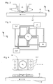
- Figure 5 shows a liquid reservoir 10 between the projection system PL and a substrate W which is positioned on the substrate stage WT.
- the liquid reservoir 10 is filled with a liquid 11 having a relatively high refractive index, e.g. water, provided via inlet/outlet ducts 13.
- the liquid has the effect that the radiation of the projection beam is a shorter wavelength in the liquid than in air or in a vacuum, allowing smaller features to be resolved.
- the resolution limit of a projection system is determined, inter alia, by the wavelength of the projection beam and the numerical aperture of the system.
- the presence of the liquid may also be regarded as increasing the effective numerical aperture.
- the liquid is effective to increase the depth of field.
- the reservoir 10 forms a preferably contactless seal to the substrate W around the image field of the projection lens PL so that the liquid is confined to fill the space between the substrate's primary surface, which faces the projection system PL, and the final element (e.g. an 'ab gleichplatte' which seals the projection system, or the final optical element of the projection system) of the projection system PL.
- the reservoir is formed by a seal member 12 positioned below and surrounding the final element of the projection lens PL.
- the liquid containment system LCS provides liquid on only a localized area of the substrate.
- the seal member 12 forms part of the liquid containment system LCS for filling the space between the final element of the projection system and the sensor 10 (or substrate W) with a liquid.
- the seal member 12 extends a little above the bottom element of the projection lens and the liquid rises above the final element so that a buffer of liquid is provided.
- the seal member 12 has an inner periphery that at the upper end closely conforms to the shape of the projection system or the final element thereof and may, e.g. be round. At the bottom the inner periphery forms an aperture which closely conforms to the shape of the image field, e.g. rectangular, though this is not necessarily so. The projection beam passes through this aperture.
- the liquid 11 is confined in the reservoir 10 by a seal device 16.
- the seal device is a contactless seal, i.e. a gas seal.
- the gas seal is formed by gas, e.g. air or synthetic air, provided under pressure via inlet 15 to the gap between seal member 12 and substrate W and extracted by first outlet 14.
- the over pressure on the gas inlet 15, vacuum level on the first outlet 14 and the geometry of the gap are arranged so that there is a high-velocity air flow inwards towards the optical axis of the apparatus that confines the liquid 11.
- some liquid is likely to escape, for example up the first outlet 14.
- Figures 2 and 3 also depict a liquid reservoir defined by inlet(s) IN, outlet(s) OUT, the substrate W and the final element of projection lens PL.
- the liquid containment system illustrated in Figures 2 and 3 comprising inlet(s) IN and outlet(s) OUT, supplies liquid to a space between the final element of the projection system and a localized area of the primary surface of the substrate.
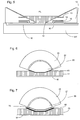
- Figure 6 illustrates in detail the final element 20 of the projection system PL.
- the final element is a final optical element 20 which comprises a first component 25 and a second component 27.
- the final element 20 of the projection system PL is comprised of first and second components 25, 27 so that the element may be made of a material which exhibits birefringence.
- a preferred material for irradiation at 157 nm is CaF2 which is transmissive but exhibits birefringence properties at this wavelength. Quartz is barely transmissive at 157nm. CaF2 is also preferred for 193nm although quartz can also be used at this wavelength.
- quartz lenses suffer from compaction at these wavelengths which can cause radiation to be focused on to small bits of the lens which discolor (go dark) and absorb more heat and so a channel can get cut.
- the birefringence exhibited by CaF2 at 157 nm can be compensated for by ensuring that the crystal orientations of the first and second components are aligned such that the intrinsic birefringence exhibited by the first component 25 is cancelled by the intrinsic birefringence exhibited by the second component 27.
- the projection PB which passes first through the first component 25 and then through the second component 27 exits the second component 27 substantially free of birefringence phenomena.
- the remaining optical elements of the projection system PL may be comprised of materials other than CaF2.
- the intensity of the projection beam is highest at the last element which is also the smallest so that it is this element which is most likely to suffer from compaction if made of quartz.
- the final element 20 of the projection system PL is substantially hemispherical in shape.
- the second component 27 is in the shape of a hemisphere and is positioned in a recess of the first component 25 which has an outer surface of the shape of a hemisphere with a recess in its non-curved surface.
- CaF2 may dissolve or react with immersion liquid 11 used in an immersion liquid lithographic projection apparatus.
- immersion liquid is envisaged as comprising substantially water for 248 and 193nm.
- perfluouro-hydrocarbons are envisaged.
- One way of protecting the final element 20 of the projection system from attack by the immersion liquid 11 is to provide a protective coating 40 on a surface of the final element 20 which is in contact with the immersion liquid.
- the material of the protective coating 40 is preferably inert in the immersion liquid 11 and does not dissolve.
- the protective coating 40 is attached to the bottom (as illustrated) surface of the second component 27 of the projection system PL.
- the protective coating is preferably between 5 and 500 nm thick, more preferably between 10 and 200 nm thick.
- material of the protective coating 40 is a metal, a metal oxide or nitride or SiO2 with a low contact angle with the immersion fluid to limit bubble inclusion.
- the layer may be deposited on the element 20 by e.g. evaporation, spluttering etc.
- a protective coating 40 is not limited to the case where the final element 20 of the projection system PL is comprised of CaF2.
- the final element is comprised of quartz (as typically in the case of an abQueryplatte being the final element)
- a protective layer 40 may also be required.
- the protective coating 40 should be as thin as possible to minimize transmission losses.
- the refractive index of the protective coating 40 can be partially varied by the deposition process and the deposition parameters. Experience gained in the deposition of EUV coatings might be usefully harnessed to optimize this process.
- Figure 7 illustrates a second embodiment of the present invention which is the same as the first embodiment except as described below.
- the liquid supply system comprises means for providing a first immersion liquid 70 which is in contact with the final element 20 of the projection system.
- a second immersion liquid 75 is also provided which is in contact with the substrate W.
- the first immersion liquid 70 can be chosen such that it only reacts with or dissolves very slowly the material of the final element 20 or does not react at all.
- the second immersion liquid 75 can then be chosen because of its good optical properties without any activity limitations being placed on it because of its contact with the final element 20.
- the two immersion liquids 70, 75 may be provided to the correct areas of the space and kept substantially apart.
- a membrane 50 is provided for separating the first and second 70, 75 immersion liquids.
- the immersion liquids 70, 75 may then be provided separately on either side of the membrane.
- the membrane is between 0.1 and 5mm thick to give the required stiffness without seriously deleteriously effecting the quality of the projection beam PB.
- suitable material for making the membrane 50 is SiO2.
- the membrane 50 may be replaceable.
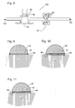
- FIG 8 illustrates a liquid supply system which may be used with either of the above two embodiments.
- the liquid supply system 100 provides liquid from an inlet 102 to a liquid containment system LCS which may be any type of liquid containment system, especially of the types illustrated in Figures 2 to 5.
- LCS liquid containment system
- the immersion liquid is provided between the ab gleichplatte 90 and the substrate W. Immersion liquid exits then via a drain 104.
- Components of the liquid containment system, the projection system PL and the substrate table WT all come in contact with the immersion liquid. If any of those components are made of a material which can dissolve in untreated immersion liquid, and are not protected, this can deleteriously effect the lifetime of the apparatus.
- a sacrificial unit 80 is provided upstream of the liquid containment system LCS in the liquid supply system 100.
- the sacrificial unit 80 at least one sacrificial body 85 is positioned.
- the sacrificial body 85 is intended to dissolve in the immersion liquid thereby to reduce the activity of the immersion liquid with materials of the components to be protected in the projection system and/or of the substrate table and/or of the liquid containment system downstream.
- the immersion liquid (which may be water) can be saturated with quartz as it passes through the sacrificial unit 80 such that the immersion liquid activity with quartz once it reaches the liquid containment system LCS and ab gleichplatte 90 is reduced.
- the sacrificial unit 80 may contain a plurality of sacrificial bodies which are not necessarily all of the same material. It may also be that the sacrificial bodies may be made of a different material to those materials which they are intended to protect. For example, a sacrificial body may be designed to reduce the pH of the immersion liquid to such a level that materials of components to be protected downstream of the sacrificial unit 80 do not dissolve. Alternatively, a buffer could be added to the liquid.
- the sacrificial bodies 85 have as large as possible a surface area to volume ratio.
- Example shapes are rods, tubes, etc.. However, clearly any shape can be used.
- the final element 20 of the projection system is protected by a fused silica plate 45.
- This plate may have a thickness in the range of form 50 ⁇ m to 5mm and may be contact bonded or glue bonded to the final element 20. In contact bonding, no glue is used - the bonding surfaces are made smooth and clean enough to directly bond together.
- the fused silica plate may be ground and polished to the desired thickness, avoiding difficulties inherent in handling a very thin plate.
- a liquid-tight seal 46 may be provided around the perimeter of the join.
- a seal 46 around the join of the final element and the fused silica protective plate is especially desirable where the final element and fused silica plate are contact bonded together.
- this form of bonding can provide an exceptionally strong bond, where dissimilar materials, such as CaF and fused silica, are bonded temperature changes and thermal gradients can cause the bond to "breathe" - differential thermal expansion or contraction of the two materials causes them to separate until the stress is relieved.
- the bond usually reforms very quickly in the case of thermal separation, if this occurs when the final element is in contact with a liquid, e.g. during polishing or grinding of the protective layer or use of the apparatus, liquid can be drawn into the gap.
- seal is a layer of SiO formed by applying a suitable precursor (such as silicone fluids (i.e. comprising Si-O chains of various lengths with various hydrocarbon side-chains), tetraethyl orthosilicate, decamethyl tetrasiloxane and tetrabutyl orthosilicate) and irradiating it with DUV light to photo-convert the precursor to SiO.
- a suitable precursor such as silicone fluids (i.e. comprising Si-O chains of various lengths with various hydrocarbon side-chains), tetraethyl orthosilicate, decamethyl tetrasiloxane and tetrabutyl orthosilicate) and irradiating it with DUV light to photo-convert the precursor to SiO.
- a suitable precursor such as silicone fluids (i.e. comprising Si-O chains of various lengths with various hydrocarbon side-chains), tetraethyl orthosilicate, decamethyl tetrasi
- seals that is useful are a silicon caulk provided over a layer of titanium oxide.
- the titanium oxide is applied by painting a precursor onto the seal and photo-converting it to titanium oxide and acts to protect the silicone caulk from UV light during operation of the apparatus.
- a further form of seal is formed by painting tetraethyl orthosilicate around the join, which then decomposes at room temperature to form a thin layer of fused silica which forms a seal. This seal is however rather brittle so that careful handling is required.
- a liquid 47 such as oil, is provided between the last lens element 20 and the protective plate 45.
- the liquid 47 preferably has a refractive index as close as possible to that of the immersion fluid 11, which may be water, but is not damaging to the material of the final lens element 20, which may be CaF 2 .
- This enables the protective plate to be interchangeable by substantially reducing the requirements on the accuracy with which the protective plate 45 must be positioned as the fluids above and below it have similar refractive indexes.
- a further variant of the present invention uses a two layer protective coating, made up of inner layer 48 and outer layer 49. It can be very difficult to form a layer of protective coating, without pinholes. Even the smallest pinhole in a protective coating applied to a CaF body allows dissolution of the CaF body when immersed in water, causing cavitation which is extremely deleterious to the optical properties of the element.
- a two layer protective coating it can be arranged that the pinholes in one layer do not match up with the pinholes in the other layer so that there is no through path in the protective layer. It can best be ensured that the pinholes of the two layers do not match up by applying the two protective layers by different methods.
- a preferred embodiment of the invention has a first layer 48 of SiO applied by sputtering and a second layer 49 applied by spin coating a precursor and photo-converting the precursor to SiO.
- This method has been found to be more effective than sputtering two layers of SiO since the pinholes in the second sputtered layer have a tendency to line up with those in the first layer.
- the spin coating and photo-conversion method provides a layer of bulk SiO rather than porous SiO.
- a layer formed by spin-coating a precursor and then photo-converting it to SiO may also be used on its own as a seal layer.
- the precursor used to form protective layer 49 may be any suitable fluid of, or containing, organo-silicon compounds. Suitable examples are silicone fluids (i.e. comprising Si-O chains of various lengths with various hydrocarbon side-chains), tetraethyl orthosilicate, decamethyl tetrasiloxane and tetrabutyl orthosilicate.
- the material may be chosen to have a desired viscosity to enable a suitably even layer to be provided by spin coating. Solvents, preferably volatile organic solvents, may be used to adjust the viscosity if necessary.
- Photo-conversion of the precursor to SiO can be achieved with irradiation by DUV light of various wavelengths, e.g. 184nm or 172nm, at a rate determined to avoid any deleterious effects that might be induced by thermal gradients in the element.
- Each of the two layers of the protective coating may have a thickness in the range of 50 to 200nm.
- lithographic apparatus in the manufacture of ICs
- the lithographic apparatus described herein may have other applications, such as the manufacture of integrated optical systems, guidance and detection patterns for magnetic domain memories, flat-panel displays, liquid-crystal displays (LCDs), thin-film magnetic heads, etc.
- LCDs liquid-crystal displays
- any use of the terms “wafer” or “die” herein may be considered as synonymous with the more general terms “substrate” or "target portion”, respectively.
- the substrate referred to herein may be processed, before or after exposure, in for example a track (a tool that typically applies a layer of resist to a substrate and develops the exposed resist), a metrology tool and/or an inspection tool. Where applicable, the disclosure herein may be applied to such and other substrate processing tools. Further, the substrate may be processed more than once, for example in order to create a multi-layer IC, so that the term substrate used herein may also refer to a substrate that already contains multiple processed layers.
- UV radiation e.g. having a wavelength of or about 365, 248, 193, 157 or 126 nm.
- lens may refer to any one or combination of various types of optical components, including refractive and reflective optical components.
- the invention may take the form of a computer program containing one or more sequences of machine-readable instructions describing a method as disclosed above, or a data storage medium (e.g. semiconductor memory, magnetic or optical disk) having such a computer program stored therein.
- a data storage medium e.g. semiconductor memory, magnetic or optical disk
- the present invention can be applied to any immersion lithography apparatus, in particular, but not exclusively, those types mentioned above.
Landscapes
- Physics & Mathematics (AREA)
- General Physics & Mathematics (AREA)
- Health & Medical Sciences (AREA)
- Engineering & Computer Science (AREA)
- Environmental & Geological Engineering (AREA)
- Epidemiology (AREA)
- Public Health (AREA)
- Exposure And Positioning Against Photoresist Photosensitive Materials (AREA)
- Exposure Of Semiconductors, Excluding Electron Or Ion Beam Exposure (AREA)
- Surface Treatment Of Optical Elements (AREA)
Priority Applications (2)
| Application Number | Priority Date | Filing Date | Title |
|---|---|---|---|
| EP10179586.2A EP2261740B1 (fr) | 2003-08-29 | 2004-08-17 | Appareil lithographique |
| EP04254940A EP1510871B1 (fr) | 2003-08-29 | 2004-08-17 | Appareil lithographique et méthode de fabrication d'un dispositif |
Applications Claiming Priority (4)
| Application Number | Priority Date | Filing Date | Title |
|---|---|---|---|
| EP03255377 | 2003-08-29 | ||
| EP03255377 | 2003-08-29 | ||
| US10/698,012 US6954256B2 (en) | 2003-08-29 | 2003-10-31 | Gradient immersion lithography |
| EP04254940A EP1510871B1 (fr) | 2003-08-29 | 2004-08-17 | Appareil lithographique et méthode de fabrication d'un dispositif |
Related Child Applications (2)
| Application Number | Title | Priority Date | Filing Date |
|---|---|---|---|
| EP10179586.2A Division EP2261740B1 (fr) | 2003-08-29 | 2004-08-17 | Appareil lithographique |
| EP10179586.2 Division-Into | 2010-09-24 |
Publications (3)
| Publication Number | Publication Date |
|---|---|
| EP1510871A2 true EP1510871A2 (fr) | 2005-03-02 |
| EP1510871A3 EP1510871A3 (fr) | 2005-04-06 |
| EP1510871B1 EP1510871B1 (fr) | 2012-04-04 |
Family
ID=34424773
Family Applications (1)
| Application Number | Title | Priority Date | Filing Date |
|---|---|---|---|
| EP04254940A Not-in-force EP1510871B1 (fr) | 2003-08-29 | 2004-08-17 | Appareil lithographique et méthode de fabrication d'un dispositif |
Country Status (5)
| Country | Link |
|---|---|
| US (2) | US6954256B2 (fr) |
| EP (1) | EP1510871B1 (fr) |
| JP (3) | JP2005079589A (fr) |
| CN (1) | CN100495213C (fr) |
| SG (1) | SG109610A1 (fr) |
Cited By (15)
| Publication number | Priority date | Publication date | Assignee | Title |
|---|---|---|---|---|
| WO2005119742A1 (fr) | 2004-06-04 | 2005-12-15 | Nikon Corporation | Appareil et procede d'exposition, et procede de production de dispositif |
| EP1670042A1 (fr) * | 2003-09-29 | 2006-06-14 | Nikon Corporation | Systeme de lentille de type a immersion dans le liquide, aligneur de projection, et procede de production du dispositif |
| EP1677153A1 (fr) * | 2004-12-28 | 2006-07-05 | ASML Netherlands B.V. | Appareil lithographique et procédé pour la production d'un dispositif |
| WO2007039374A2 (fr) * | 2005-09-30 | 2007-04-12 | International Business Machines Corporation | Systeme de lithographie optique par immersion pourvu d'un revetement optique protecteur |
| GB2431670A (en) * | 2005-10-25 | 2007-05-02 | Zeiss Carl Smt Ag | Protective coating with windows for protection of optical element that is soluble in immersion liquid. |
| EP1860507A1 (fr) * | 2006-05-22 | 2007-11-28 | ASML Netherlands BV | Appareil lithographique et procédé de nettoyage d'appareil lithographique |
| WO2007144125A2 (fr) * | 2006-06-13 | 2007-12-21 | Carl-Zeiss Smt Ag | Dispositif de reproduction |
| WO2009128554A1 (fr) * | 2008-04-14 | 2009-10-22 | Nikon Corporation | Appareil d'exposition, procédé de nettoyage et procédé de production de dispositif |
| US7697111B2 (en) | 2003-08-26 | 2010-04-13 | Nikon Corporation | Optical element and exposure apparatus |
| US7876418B2 (en) | 2002-12-10 | 2011-01-25 | Nikon Corporation | Optical element and projection exposure apparatus based on use of the optical element |
| US8149381B2 (en) | 2003-08-26 | 2012-04-03 | Nikon Corporation | Optical element and exposure apparatus |
| US8208123B2 (en) | 2003-08-29 | 2012-06-26 | Asml Netherlands B.V. | Lithographic apparatus and device manufacturing method |
| CN102540766A (zh) * | 2006-09-12 | 2012-07-04 | 卡尔蔡司Smt有限责任公司 | 用于浸入式光刻的光学装置及包含该装置的投影曝光设备 |
| EP1739801B1 (fr) * | 2005-06-30 | 2013-01-23 | Corning Incorporated | Optiques de lasers excimères, à durée de vie étendue |
| CN105022239A (zh) * | 2014-04-25 | 2015-11-04 | 上海微电子装备有限公司 | 背面对准装置及对准方法 |
Families Citing this family (233)
| Publication number | Priority date | Publication date | Assignee | Title |
|---|---|---|---|---|
| WO2004019128A2 (fr) * | 2002-08-23 | 2004-03-04 | Nikon Corporation | Systeme optique de projection et procede associe pour la photolithographie, et appareil d'exposition et procede associe |
| US7081278B2 (en) * | 2002-09-25 | 2006-07-25 | Asml Holdings N.V. | Method for protection of adhesives used to secure optics from ultra-violet light |
| US9482966B2 (en) | 2002-11-12 | 2016-11-01 | Asml Netherlands B.V. | Lithographic apparatus and device manufacturing method |
| US7372541B2 (en) * | 2002-11-12 | 2008-05-13 | Asml Netherlands B.V. | Lithographic apparatus and device manufacturing method |
| SG121822A1 (en) * | 2002-11-12 | 2006-05-26 | Asml Netherlands Bv | Lithographic apparatus and device manufacturing method |
| US10503084B2 (en) | 2002-11-12 | 2019-12-10 | Asml Netherlands B.V. | Lithographic apparatus and device manufacturing method |
| US7110081B2 (en) * | 2002-11-12 | 2006-09-19 | Asml Netherlands B.V. | Lithographic apparatus and device manufacturing method |
| DE60335595D1 (de) | 2002-11-12 | 2011-02-17 | Asml Netherlands Bv | Lithographischer Apparat mit Immersion und Verfahren zur Herstellung einer Vorrichtung |
| CN100568101C (zh) | 2002-11-12 | 2009-12-09 | Asml荷兰有限公司 | 光刻装置和器件制造方法 |
| SG135052A1 (en) | 2002-11-12 | 2007-09-28 | Asml Netherlands Bv | Lithographic apparatus and device manufacturing method |
| CN101424883B (zh) * | 2002-12-10 | 2013-05-15 | 株式会社尼康 | 曝光设备和器件制造法 |
| US7948604B2 (en) * | 2002-12-10 | 2011-05-24 | Nikon Corporation | Exposure apparatus and method for producing device |
| KR101085372B1 (ko) * | 2002-12-10 | 2011-11-21 | 가부시키가이샤 니콘 | 노광 장치 및 디바이스 제조 방법 |
| JP4352874B2 (ja) * | 2002-12-10 | 2009-10-28 | 株式会社ニコン | 露光装置及びデバイス製造方法 |
| KR101101737B1 (ko) * | 2002-12-10 | 2012-01-05 | 가부시키가이샤 니콘 | 노광장치 및 노광방법, 디바이스 제조방법 |
| EP1571695A4 (fr) | 2002-12-10 | 2008-10-15 | Nikon Corp | Appareil d'exposition et son procede de fabrication |
| US7242455B2 (en) * | 2002-12-10 | 2007-07-10 | Nikon Corporation | Exposure apparatus and method for producing device |
| ATE365962T1 (de) | 2002-12-19 | 2007-07-15 | Koninkl Philips Electronics Nv | Verfahren und anordnung zum bestrahlen einer schicht mittels eines lichtpunkts |
| DE10261775A1 (de) | 2002-12-20 | 2004-07-01 | Carl Zeiss Smt Ag | Vorrichtung zur optischen Vermessung eines Abbildungssystems |
| SG183572A1 (en) * | 2003-02-26 | 2012-09-27 | Nikon Corp | Exposure apparatus, exposure method, and method for producing device |
| KR20050110033A (ko) * | 2003-03-25 | 2005-11-22 | 가부시키가이샤 니콘 | 노광 장치 및 디바이스 제조 방법 |
| EP1612850B1 (fr) * | 2003-04-07 | 2009-03-25 | Nikon Corporation | Appareil d'exposition et procede pour fabrication d'un dispositif |
| JP4488004B2 (ja) * | 2003-04-09 | 2010-06-23 | 株式会社ニコン | 液浸リソグラフィ流体制御システム |
| KR101745223B1 (ko) | 2003-04-10 | 2017-06-08 | 가부시키가이샤 니콘 | 액침 리소그래피 장치용 운반 영역을 포함하는 환경 시스템 |
| EP2950147B1 (fr) * | 2003-04-10 | 2017-04-26 | Nikon Corporation | Système environnemental incluant un systéme de recirculation sous vide pour un appareil de lithographie par immersion |
| JP4488005B2 (ja) | 2003-04-10 | 2010-06-23 | 株式会社ニコン | 液浸リソグラフィ装置用の液体を捕集するための流出通路 |
| JP4656057B2 (ja) * | 2003-04-10 | 2011-03-23 | 株式会社ニコン | 液浸リソグラフィ装置用電気浸透素子 |
| KR20170016014A (ko) * | 2003-04-11 | 2017-02-10 | 가부시키가이샤 니콘 | 액침 리소그래피에 의한 광학기기의 세정방법 |
| WO2004092830A2 (fr) | 2003-04-11 | 2004-10-28 | Nikon Corporation | Systeme de projection et de recuperation de liquides pour lithographie par immersion |
| CN101002140B (zh) | 2003-04-11 | 2010-12-08 | 株式会社尼康 | 保持平板印刷投射透镜下面的浸没流体的设备和方法 |
| KR101369582B1 (ko) * | 2003-04-17 | 2014-03-04 | 가부시키가이샤 니콘 | 액침 리소그래피에서 이용하기 위한 오토포커스 소자의 광학적 배열 |
| KR101521407B1 (ko) | 2003-05-06 | 2015-05-18 | 가부시키가이샤 니콘 | 투영 광학계, 노광 장치 및 노광 방법 |
| US7348575B2 (en) | 2003-05-06 | 2008-03-25 | Nikon Corporation | Projection optical system, exposure apparatus, and exposure method |
| TWI295414B (en) * | 2003-05-13 | 2008-04-01 | Asml Netherlands Bv | Lithographic apparatus and device manufacturing method |
| WO2004102646A1 (fr) * | 2003-05-15 | 2004-11-25 | Nikon Corporation | Appareil d'exposition et procede de fabrication de dispositif |
| TWI424470B (zh) | 2003-05-23 | 2014-01-21 | 尼康股份有限公司 | A method of manufacturing an exposure apparatus and an element |
| TW201515064A (zh) | 2003-05-23 | 2015-04-16 | 尼康股份有限公司 | 曝光方法及曝光裝置以及元件製造方法 |
| KR101548832B1 (ko) | 2003-05-28 | 2015-09-01 | 가부시키가이샤 니콘 | 노광 방법, 노광 장치, 및 디바이스 제조 방법 |
| TWI442694B (zh) * | 2003-05-30 | 2014-06-21 | Asml Netherlands Bv | 微影裝置及元件製造方法 |
| US7213963B2 (en) * | 2003-06-09 | 2007-05-08 | Asml Netherlands B.V. | Lithographic apparatus and device manufacturing method |
| US7317504B2 (en) * | 2004-04-08 | 2008-01-08 | Asml Netherlands B.V. | Lithographic apparatus and device manufacturing method |
| EP1486827B1 (fr) | 2003-06-11 | 2011-11-02 | ASML Netherlands B.V. | Appareil lithographique et méthode de fabrication d'un dispositif |
| EP3104396B1 (fr) | 2003-06-13 | 2018-03-21 | Nikon Corporation | Procede et appareil d'exposition, etape de substrat et procede de fabrication de dispositif |
| TWI433211B (zh) | 2003-06-19 | 2014-04-01 | 尼康股份有限公司 | A method of manufacturing an exposure apparatus and an element |
| WO2005006026A2 (fr) * | 2003-07-01 | 2005-01-20 | Nikon Corporation | Utilisation de fluides specifies isotopiquement comme elements optiques |
| JP4697138B2 (ja) * | 2003-07-08 | 2011-06-08 | 株式会社ニコン | 液浸リソグラフィ装置、液浸リソグラフィ方法、デバイス製造方法 |
| EP2264531B1 (fr) | 2003-07-09 | 2013-01-16 | Nikon Corporation | Appareil d'exposition et procédé de fabrication d'un dispositif |
| WO2005006418A1 (fr) * | 2003-07-09 | 2005-01-20 | Nikon Corporation | Dispositif d'exposition et procede de fabrication |
| EP1643543B1 (fr) * | 2003-07-09 | 2010-11-24 | Nikon Corporation | Appareil d'exposition, et procede de fabrication d'un dispositif |
| US7738074B2 (en) | 2003-07-16 | 2010-06-15 | Asml Netherlands B.V. | Lithographic apparatus and device manufacturing method |
| EP1500982A1 (fr) | 2003-07-24 | 2005-01-26 | ASML Netherlands B.V. | Appareil lithographique et méthode de fabrication d'un dispositif |
| WO2005010960A1 (fr) * | 2003-07-25 | 2005-02-03 | Nikon Corporation | Systeme d'inspection , dispositif d'inspection et procede de production pour systeme de projection optique |
| EP1503244A1 (fr) | 2003-07-28 | 2005-02-02 | ASML Netherlands B.V. | Appareil de projection lithographique et méthode de fabrication d'un dispositif |
| US7326522B2 (en) | 2004-02-11 | 2008-02-05 | Asml Netherlands B.V. | Device manufacturing method and a substrate |
| US7175968B2 (en) * | 2003-07-28 | 2007-02-13 | Asml Netherlands B.V. | Lithographic apparatus, device manufacturing method and a substrate |
| KR101403117B1 (ko) * | 2003-07-28 | 2014-06-03 | 가부시키가이샤 니콘 | 노광 장치 및 디바이스 제조 방법, 그리고 노광 장치의 제어 방법 |
| US7779781B2 (en) | 2003-07-31 | 2010-08-24 | Asml Netherlands B.V. | Lithographic apparatus and device manufacturing method |
| WO2005022616A1 (fr) * | 2003-08-29 | 2005-03-10 | Nikon Corporation | Appareil d'exposition et procede de production d'un dispositif |
| EP2261740B1 (fr) | 2003-08-29 | 2014-07-09 | ASML Netherlands BV | Appareil lithographique |
| TWI245163B (en) | 2003-08-29 | 2005-12-11 | Asml Netherlands Bv | Lithographic apparatus and device manufacturing method |
| TWI263859B (en) * | 2003-08-29 | 2006-10-11 | Asml Netherlands Bv | Lithographic apparatus and device manufacturing method |
| KR101748923B1 (ko) | 2003-09-03 | 2017-06-19 | 가부시키가이샤 니콘 | 액침 리소그래피용 유체를 제공하기 위한 장치 및 방법 |
| WO2005029559A1 (fr) * | 2003-09-19 | 2005-03-31 | Nikon Corporation | Appareil d'insolation et procede permettant de produire un dispositif |
| KR20170058458A (ko) | 2003-09-29 | 2017-05-26 | 가부시키가이샤 니콘 | 노광장치, 노광방법 및 디바이스 제조방법 |
| US7369217B2 (en) * | 2003-10-03 | 2008-05-06 | Micronic Laser Systems Ab | Method and device for immersion lithography |
| JP4335213B2 (ja) | 2003-10-08 | 2009-09-30 | 株式会社蔵王ニコン | 基板搬送装置、露光装置、デバイス製造方法 |
| ATE509367T1 (de) | 2003-10-08 | 2011-05-15 | Zao Nikon Co Ltd | Belichtungsgerät, substrattrageverfahren, belichtungsverfahren und verfahren zur herstellung einer vorrichtung |
| JP2005136364A (ja) * | 2003-10-08 | 2005-05-26 | Zao Nikon Co Ltd | 基板搬送装置、露光装置、並びにデバイス製造方法 |
| TW201738932A (zh) * | 2003-10-09 | 2017-11-01 | Nippon Kogaku Kk | 曝光裝置及曝光方法、元件製造方法 |
| EP1524558A1 (fr) * | 2003-10-15 | 2005-04-20 | ASML Netherlands B.V. | Appareil lithographique et procédé pour la production d'un dispositif |
| EP1524557A1 (fr) | 2003-10-15 | 2005-04-20 | ASML Netherlands B.V. | Appareil lithographique et méthode de fabrication d'un dispositif |
| US7411653B2 (en) | 2003-10-28 | 2008-08-12 | Asml Netherlands B.V. | Lithographic apparatus |
| US7352433B2 (en) | 2003-10-28 | 2008-04-01 | Asml Netherlands B.V. | Lithographic apparatus and device manufacturing method |
| US7924397B2 (en) * | 2003-11-06 | 2011-04-12 | Taiwan Semiconductor Manufacturing Company, Ltd. | Anti-corrosion layer on objective lens for liquid immersion lithography applications |
| US7528929B2 (en) | 2003-11-14 | 2009-05-05 | Asml Netherlands B.V. | Lithographic apparatus and device manufacturing method |
| US7545481B2 (en) | 2003-11-24 | 2009-06-09 | Asml Netherlands B.V. | Lithographic apparatus and device manufacturing method |
| TWI596442B (zh) * | 2003-12-03 | 2017-08-21 | 尼康股份有限公司 | Exposure apparatus, exposure method, device manufacturing method |
| JP2005175034A (ja) * | 2003-12-09 | 2005-06-30 | Canon Inc | 露光装置 |
| JP4907596B2 (ja) * | 2003-12-15 | 2012-03-28 | カール・ツァイス・エスエムティー・ゲーエムベーハー | 屈折性投影対物レンズ |
| WO2005106589A1 (fr) * | 2004-05-04 | 2005-11-10 | Carl Zeiss Smt Ag | Appareil d'exposition par projection microlithographique, et liquide d'immersion destine a l'appareil |
| US20070081133A1 (en) * | 2004-12-14 | 2007-04-12 | Niikon Corporation | Projection exposure apparatus and stage unit, and exposure method |
| KR101111363B1 (ko) * | 2003-12-15 | 2012-04-12 | 가부시키가이샤 니콘 | 투영노광장치 및 스테이지 장치, 그리고 노광방법 |
| EP1699073B1 (fr) * | 2003-12-15 | 2010-12-08 | Nikon Corporation | Systeme de platine, appareil d'exposition et procede d'exposition |
| JP2005189850A (ja) * | 2003-12-15 | 2005-07-14 | Carl Zeiss Smt Ag | 液浸リソグラフィー用屈折性投影対物レンズ |
| US7460206B2 (en) * | 2003-12-19 | 2008-12-02 | Carl Zeiss Smt Ag | Projection objective for immersion lithography |
| US7394521B2 (en) * | 2003-12-23 | 2008-07-01 | Asml Netherlands B.V. | Lithographic apparatus and device manufacturing method |
| US7589818B2 (en) * | 2003-12-23 | 2009-09-15 | Asml Netherlands B.V. | Lithographic apparatus, alignment apparatus, device manufacturing method, and a method of converting an apparatus |
| JP2005191394A (ja) * | 2003-12-26 | 2005-07-14 | Canon Inc | 露光方法及び装置 |
| JP2005195878A (ja) * | 2004-01-07 | 2005-07-21 | Olympus Corp | 対物レンズ、光分析装置、光分析装置の運転方法および顕微鏡 |
| WO2005071491A2 (fr) * | 2004-01-20 | 2005-08-04 | Carl Zeiss Smt Ag | Appareil microlithographique d'insolation par projection et dispositif de mesure pour objectif de projection |
| US20050161644A1 (en) * | 2004-01-23 | 2005-07-28 | Peng Zhang | Immersion lithography fluids |
| TWI259319B (en) * | 2004-01-23 | 2006-08-01 | Air Prod & Chem | Immersion lithography fluids |
| US7589822B2 (en) | 2004-02-02 | 2009-09-15 | Nikon Corporation | Stage drive method and stage unit, exposure apparatus, and device manufacturing method |
| KR101377815B1 (ko) | 2004-02-03 | 2014-03-26 | 가부시키가이샤 니콘 | 노광 장치 및 디바이스 제조 방법 |
| US7050146B2 (en) | 2004-02-09 | 2006-05-23 | Asml Netherlands B.V. | Lithographic apparatus and device manufacturing method |
| JP4370992B2 (ja) * | 2004-02-18 | 2009-11-25 | 株式会社ニコン | 光学素子及び露光装置 |
| TWI395069B (zh) * | 2004-02-18 | 2013-05-01 | 尼康股份有限公司 | 投影光學系統、曝光裝置以及曝光方法 |
| US20080038675A1 (en) * | 2004-02-20 | 2008-02-14 | Nikon Corporation | Exposure Method, Exposure Apparatus, Exposure System and Device Manufacturing Method |
| TWI518744B (zh) * | 2004-03-25 | 2016-01-21 | 尼康股份有限公司 | 曝光裝置、曝光方法、及元件製造方法 |
| JP4510494B2 (ja) * | 2004-03-29 | 2010-07-21 | キヤノン株式会社 | 露光装置 |
| US7034917B2 (en) * | 2004-04-01 | 2006-04-25 | Asml Netherlands B.V. | Lithographic apparatus, device manufacturing method and device manufactured thereby |
| US7898642B2 (en) * | 2004-04-14 | 2011-03-01 | Asml Netherlands B.V. | Lithographic apparatus and device manufacturing method |
| US20050231695A1 (en) * | 2004-04-15 | 2005-10-20 | Taiwan Semiconductor Manufacturing Company, Ltd. | Method and system for immersion lithography using high PH immersion fluid |
| US7271878B2 (en) * | 2004-04-22 | 2007-09-18 | International Business Machines Corporation | Wafer cell for immersion lithography |
| EP1747499A2 (fr) | 2004-05-04 | 2007-01-31 | Nikon Corporation | Appareil et procede d'approvisionnement en fluide pour la lithographie par immersion |
| US7616383B2 (en) * | 2004-05-18 | 2009-11-10 | Asml Netherlands B.V. | Lithographic apparatus and device manufacturing method |
| US7486381B2 (en) * | 2004-05-21 | 2009-02-03 | Asml Netherlands B.V. | Lithographic apparatus and device manufacturing method |
| JP4655763B2 (ja) * | 2004-06-04 | 2011-03-23 | 株式会社ニコン | 露光装置、露光方法及びデバイス製造方法 |
| US20070103661A1 (en) * | 2004-06-04 | 2007-05-10 | Nikon Corporation | Exposure apparatus, exposure method, and method for producing device |
| CN101833247B (zh) | 2004-06-04 | 2013-11-06 | 卡尔蔡司Smt有限责任公司 | 微光刻投影曝光系统的投影物镜的光学测量的测量系统 |
| EP3203498A1 (fr) * | 2004-06-09 | 2017-08-09 | Nikon Corporation | Appareil d'exposition et procédé de fabrication du dispositif |
| US20070222959A1 (en) * | 2004-06-10 | 2007-09-27 | Nikon Corporation | Exposure apparatus, exposure method, and method for producing device |
| US20080068567A1 (en) * | 2004-06-10 | 2008-03-20 | Hiroyuki Nagasaka | Exposure Apparatus, Exposure Method, and Method for Producing Device |
| US7481867B2 (en) * | 2004-06-16 | 2009-01-27 | Edwards Limited | Vacuum system for immersion photolithography |
| US7180572B2 (en) * | 2004-06-23 | 2007-02-20 | Taiwan Semiconductor Manufacturing Company, Ltd. | Immersion optical projection system |
| US7463330B2 (en) | 2004-07-07 | 2008-12-09 | Asml Netherlands B.V. | Lithographic apparatus and device manufacturing method |
| US8384874B2 (en) * | 2004-07-12 | 2013-02-26 | Nikon Corporation | Immersion exposure apparatus and device manufacturing method to detect if liquid on base member |
| US7304715B2 (en) | 2004-08-13 | 2007-12-04 | Asml Netherlands B.V. | Lithographic apparatus and device manufacturing method |
| US8305553B2 (en) * | 2004-08-18 | 2012-11-06 | Nikon Corporation | Exposure apparatus and device manufacturing method |
| US7701550B2 (en) | 2004-08-19 | 2010-04-20 | Asml Netherlands B.V. | Lithographic apparatus and device manufacturing method |
| US7522261B2 (en) * | 2004-09-24 | 2009-04-21 | Asml Netherlands B.V. | Lithographic apparatus and device manufacturing method |
| US7355674B2 (en) * | 2004-09-28 | 2008-04-08 | Asml Netherlands B.V. | Lithographic apparatus, device manufacturing method and computer program product |
| US7894040B2 (en) * | 2004-10-05 | 2011-02-22 | Asml Netherlands B.V. | Lithographic apparatus and device manufacturing method |
| US7379155B2 (en) | 2004-10-18 | 2008-05-27 | Asml Netherlands B.V. | Lithographic apparatus and device manufacturing method |
| US7414699B2 (en) * | 2004-11-12 | 2008-08-19 | Asml Netherlands B.V. | Lithographic apparatus and device manufacturing method |
| US7423720B2 (en) | 2004-11-12 | 2008-09-09 | Asml Netherlands B.V. | Lithographic apparatus and device manufacturing method |
| US7583357B2 (en) * | 2004-11-12 | 2009-09-01 | Asml Netherlands B.V. | Lithographic apparatus and device manufacturing method |
| US7411657B2 (en) | 2004-11-17 | 2008-08-12 | Asml Netherlands B.V. | Lithographic apparatus and device manufacturing method |
| KR101191056B1 (ko) * | 2004-11-19 | 2012-10-15 | 가부시키가이샤 니콘 | 메인터넌스 방법, 노광 방법, 노광 장치 및 디바이스 제조 방법 |
| US7161654B2 (en) * | 2004-12-02 | 2007-01-09 | Asml Netherlands B.V. | Lithographic apparatus and device manufacturing method |
| US7256121B2 (en) * | 2004-12-02 | 2007-08-14 | Texas Instruments Incorporated | Contact resistance reduction by new barrier stack process |
| US7446850B2 (en) * | 2004-12-03 | 2008-11-04 | Asml Netherlands B.V. | Lithographic apparatus and device manufacturing method |
| US7196770B2 (en) * | 2004-12-07 | 2007-03-27 | Asml Netherlands B.V. | Prewetting of substrate before immersion exposure |
| US7397533B2 (en) | 2004-12-07 | 2008-07-08 | Asml Netherlands B.V. | Lithographic apparatus and device manufacturing method |
| US7365827B2 (en) | 2004-12-08 | 2008-04-29 | Asml Netherlands B.V. | Lithographic apparatus and device manufacturing method |
| US7352440B2 (en) | 2004-12-10 | 2008-04-01 | Asml Netherlands B.V. | Substrate placement in immersion lithography |
| US7403261B2 (en) | 2004-12-15 | 2008-07-22 | Asml Netherlands B.V. | Lithographic apparatus and device manufacturing method |
| US7880860B2 (en) * | 2004-12-20 | 2011-02-01 | Asml Netherlands B.V. | Lithographic apparatus and device manufacturing method |
| US7528931B2 (en) * | 2004-12-20 | 2009-05-05 | Asml Netherlands B.V. | Lithographic apparatus and device manufacturing method |
| US7491661B2 (en) * | 2004-12-28 | 2009-02-17 | Asml Netherlands B.V. | Device manufacturing method, top coat material and substrate |
| US20060147821A1 (en) | 2004-12-30 | 2006-07-06 | Asml Netherlands B.V. | Lithographic apparatus and device manufacturing method |
| US7450217B2 (en) * | 2005-01-12 | 2008-11-11 | Asml Netherlands B.V. | Exposure apparatus, coatings for exposure apparatus, lithographic apparatus, device manufacturing method, and device manufactured thereby |
| SG124351A1 (en) | 2005-01-14 | 2006-08-30 | Asml Netherlands Bv | Lithographic apparatus and device manufacturing method |
| SG124359A1 (en) | 2005-01-14 | 2006-08-30 | Asml Netherlands Bv | Lithographic apparatus and device manufacturing method |
| US8692973B2 (en) * | 2005-01-31 | 2014-04-08 | Nikon Corporation | Exposure apparatus and method for producing device |
| US20090262316A1 (en) | 2005-01-31 | 2009-10-22 | Nikon Corporation | Exposure apparatus and method for producing device |
| JP2006222222A (ja) * | 2005-02-09 | 2006-08-24 | Canon Inc | 投影光学系及びそれを有する露光装置 |
| JP5162254B2 (ja) * | 2005-02-10 | 2013-03-13 | エーエスエムエル ネザーランズ ビー.ブイ. | 液浸リソグラフィシステム及びデバイス製造方法 |
| US8018573B2 (en) | 2005-02-22 | 2011-09-13 | Asml Netherlands B.V. | Lithographic apparatus and device manufacturing method |
| US7378025B2 (en) * | 2005-02-22 | 2008-05-27 | Asml Netherlands B.V. | Fluid filtration method, fluid filtered thereby, lithographic apparatus and device manufacturing method |
| US7224431B2 (en) * | 2005-02-22 | 2007-05-29 | Asml Netherlands B.V. | Lithographic apparatus and device manufacturing method |
| US7282701B2 (en) * | 2005-02-28 | 2007-10-16 | Asml Netherlands B.V. | Sensor for use in a lithographic apparatus |
| US7428038B2 (en) * | 2005-02-28 | 2008-09-23 | Asml Netherlands B.V. | Lithographic apparatus, device manufacturing method and apparatus for de-gassing a liquid |
| US7324185B2 (en) | 2005-03-04 | 2008-01-29 | Asml Netherlands B.V. | Lithographic apparatus and device manufacturing method |
| US7684010B2 (en) * | 2005-03-09 | 2010-03-23 | Asml Netherlands B.V. | Lithographic apparatus, device manufacturing method, seal structure, method of removing an object and a method of sealing |
| JP2006261606A (ja) * | 2005-03-18 | 2006-09-28 | Canon Inc | 露光装置、露光方法及びデバイス製造方法 |
| US7330238B2 (en) * | 2005-03-28 | 2008-02-12 | Asml Netherlands, B.V. | Lithographic apparatus, immersion projection apparatus and device manufacturing method |
| US7411654B2 (en) * | 2005-04-05 | 2008-08-12 | Asml Netherlands B.V. | Lithographic apparatus and device manufacturing method |
| USRE43576E1 (en) | 2005-04-08 | 2012-08-14 | Asml Netherlands B.V. | Dual stage lithographic apparatus and device manufacturing method |
| US7291850B2 (en) * | 2005-04-08 | 2007-11-06 | Asml Netherlands B.V. | Lithographic apparatus and device manufacturing method |
| KR20080005376A (ko) * | 2005-04-28 | 2008-01-11 | 가부시키가이샤 니콘 | 노광 방법 및 노광 장치, 그리고 디바이스 제조 방법 |
| US7317507B2 (en) * | 2005-05-03 | 2008-01-08 | Asml Netherlands B.V. | Lithographic apparatus and device manufacturing method |
| US7433016B2 (en) | 2005-05-03 | 2008-10-07 | Asml Netherlands B.V. | Lithographic apparatus and device manufacturing method |
| US8248577B2 (en) * | 2005-05-03 | 2012-08-21 | Asml Netherlands B.V. | Lithographic apparatus and device manufacturing method |
| DE102005024163A1 (de) * | 2005-05-23 | 2006-11-30 | Carl Zeiss Smt Ag | Optisches System einer mikrolithographischen Projektionsbelichtungsanlage |
| WO2006126522A1 (fr) * | 2005-05-24 | 2006-11-30 | Nikon Corporation | Procede et appareil d'exposition, et procede de fabrication du dispositif |
| DE102006021161A1 (de) * | 2005-05-25 | 2006-11-30 | Carl Zeiss Smt Ag | Projektionsobjektiv insbesondere für die Mirkolithographie |
| DE102005024682A1 (de) * | 2005-05-30 | 2006-12-14 | Schott Ag | Optisches Material aus kristallisiertem Erdalkalimetallfluorid mit erhöhtem Brechungsindex |
| KR100638107B1 (ko) * | 2005-06-09 | 2006-10-24 | 연세대학교 산학협력단 | 이머젼 박막층을 구비하는 광변조 미세개구 어레이 장치 및이를 이용한 고속 미세패턴 기록시스템 |
| US7385673B2 (en) * | 2005-06-10 | 2008-06-10 | International Business Machines Corporation | Immersion lithography with equalized pressure on at least projection optics component and wafer |
| US7652746B2 (en) * | 2005-06-21 | 2010-01-26 | Asml Netherlands B.V. | Lithographic apparatus and device manufacturing method |
| US7751027B2 (en) | 2005-06-21 | 2010-07-06 | Asml Netherlands B.V. | Lithographic apparatus and device manufacturing method |
| US7834974B2 (en) | 2005-06-28 | 2010-11-16 | Asml Netherlands B.V. | Lithographic apparatus and device manufacturing method |
| US7468779B2 (en) * | 2005-06-28 | 2008-12-23 | Asml Netherlands B.V. | Lithographic apparatus and device manufacturing method |
| US7474379B2 (en) | 2005-06-28 | 2009-01-06 | Asml Netherlands B.V. | Lithographic apparatus and device manufacturing method |
| US7351348B2 (en) * | 2005-08-10 | 2008-04-01 | International Business Machines Corporation | Evaporation control using coating |
| US7535644B2 (en) * | 2005-08-12 | 2009-05-19 | Asml Netherlands B.V. | Lens element, lithographic apparatus, device manufacturing method, and device manufactured thereby |
| US8054445B2 (en) * | 2005-08-16 | 2011-11-08 | Asml Netherlands B.V. | Lithographic apparatus and device manufacturing method |
| JP4923480B2 (ja) * | 2005-08-23 | 2012-04-25 | 株式会社ニコン | 露光装置及びデバイス製造方法、計測部材 |
| US20070058263A1 (en) * | 2005-09-13 | 2007-03-15 | Taiwan Semiconductor Manufacturing Company, Ltd. | Apparatus and methods for immersion lithography |
| US20070070323A1 (en) * | 2005-09-21 | 2007-03-29 | Nikon Corporation | Exposure apparatus, exposure method, and device fabricating method |
| US7357768B2 (en) * | 2005-09-22 | 2008-04-15 | William Marshall | Recliner exerciser |
| US7411658B2 (en) | 2005-10-06 | 2008-08-12 | Asml Netherlands B.V. | Lithographic apparatus and device manufacturing method |
| US20070127135A1 (en) * | 2005-11-01 | 2007-06-07 | Nikon Corporation | Exposure apparatus, exposure method and device manufacturing method |
| US7804577B2 (en) | 2005-11-16 | 2010-09-28 | Asml Netherlands B.V. | Lithographic apparatus |
| US7864292B2 (en) | 2005-11-16 | 2011-01-04 | Asml Netherlands B.V. | Lithographic apparatus and device manufacturing method |
| US7656501B2 (en) * | 2005-11-16 | 2010-02-02 | Asml Netherlands B.V. | Lithographic apparatus |
| US7633073B2 (en) * | 2005-11-23 | 2009-12-15 | Asml Netherlands B.V. | Lithographic apparatus and device manufacturing method |
| US7773195B2 (en) * | 2005-11-29 | 2010-08-10 | Asml Holding N.V. | System and method to increase surface tension and contact angle in immersion lithography |
| US20070124987A1 (en) * | 2005-12-05 | 2007-06-07 | Brown Jeffrey K | Electronic pest control apparatus |
| KR100768849B1 (ko) * | 2005-12-06 | 2007-10-22 | 엘지전자 주식회사 | 계통 연계형 연료전지 시스템의 전원공급장치 및 방법 |
| JP5027154B2 (ja) * | 2005-12-22 | 2012-09-19 | フリースケール セミコンダクター インコーポレイテッド | 液浸露光装置及び液浸露光方法 |
| US7420194B2 (en) * | 2005-12-27 | 2008-09-02 | Asml Netherlands B.V. | Lithographic apparatus and substrate edge seal |
| US7839483B2 (en) * | 2005-12-28 | 2010-11-23 | Asml Netherlands B.V. | Lithographic apparatus, device manufacturing method and a control system |
| US7649611B2 (en) * | 2005-12-30 | 2010-01-19 | Asml Netherlands B.V. | Lithographic apparatus and device manufacturing method |
| US8045134B2 (en) | 2006-03-13 | 2011-10-25 | Asml Netherlands B.V. | Lithographic apparatus, control system and device manufacturing method |
| CN100590173C (zh) * | 2006-03-24 | 2010-02-17 | 北京有色金属研究总院 | 一种荧光粉及其制造方法和所制成的电光源 |
| US9477158B2 (en) * | 2006-04-14 | 2016-10-25 | Asml Netherlands B.V. | Lithographic apparatus and device manufacturing method |
| DE102006021797A1 (de) * | 2006-05-09 | 2007-11-15 | Carl Zeiss Smt Ag | Optische Abbildungseinrichtung mit thermischer Dämpfung |
| JP2008042004A (ja) * | 2006-08-08 | 2008-02-21 | Tokyo Electron Ltd | パターン形成方法およびパターン形成装置 |
| US7567338B2 (en) * | 2006-08-30 | 2009-07-28 | Asml Netherlands B.V. | Lithographic apparatus and device manufacturing method |
| US7964522B2 (en) * | 2006-08-31 | 2011-06-21 | Corning Incorporated | F-doped silica glass and process of making same |
| US8045135B2 (en) | 2006-11-22 | 2011-10-25 | Asml Netherlands B.V. | Lithographic apparatus with a fluid combining unit and related device manufacturing method |
| US20080138631A1 (en) * | 2006-12-06 | 2008-06-12 | International Business Machines Corporation | Method to reduce mechanical wear of immersion lithography apparatus |
| US8634053B2 (en) | 2006-12-07 | 2014-01-21 | Asml Netherlands B.V. | Lithographic apparatus and device manufacturing method |
| US9632425B2 (en) * | 2006-12-07 | 2017-04-25 | Asml Holding N.V. | Lithographic apparatus, a dryer and a method of removing liquid from a surface |
| US7791709B2 (en) * | 2006-12-08 | 2010-09-07 | Asml Netherlands B.V. | Substrate support and lithographic process |
| US8654305B2 (en) * | 2007-02-15 | 2014-02-18 | Asml Holding N.V. | Systems and methods for insitu lens cleaning in immersion lithography |
| US8817226B2 (en) | 2007-02-15 | 2014-08-26 | Asml Holding N.V. | Systems and methods for insitu lens cleaning using ozone in immersion lithography |
| JP2008218653A (ja) * | 2007-03-02 | 2008-09-18 | Canon Inc | 露光装置及びデバイス製造方法 |
| US8237911B2 (en) | 2007-03-15 | 2012-08-07 | Nikon Corporation | Apparatus and methods for keeping immersion fluid adjacent to an optical assembly during wafer exchange in an immersion lithography machine |
| US7969555B2 (en) * | 2007-03-16 | 2011-06-28 | Industry-Academic Cooperation Foundation, Yonsei University | Lens structure, optical system having the same, and lithography method using the optical system |
| US8947629B2 (en) | 2007-05-04 | 2015-02-03 | Asml Netherlands B.V. | Cleaning device, a lithographic apparatus and a lithographic apparatus cleaning method |
| US7866330B2 (en) * | 2007-05-04 | 2011-01-11 | Asml Netherlands B.V. | Cleaning device, a lithographic apparatus and a lithographic apparatus cleaning method |
| US8011377B2 (en) | 2007-05-04 | 2011-09-06 | Asml Netherlands B.V. | Cleaning device and a lithographic apparatus cleaning method |
| US7900641B2 (en) * | 2007-05-04 | 2011-03-08 | Asml Netherlands B.V. | Cleaning device and a lithographic apparatus cleaning method |
| US7561250B2 (en) * | 2007-06-19 | 2009-07-14 | Asml Netherlands B.V. | Lithographic apparatus having parts with a coated film adhered thereto |
| TWI389551B (zh) * | 2007-08-09 | 2013-03-11 | Mstar Semiconductor Inc | 迦瑪校正裝置 |
| NL1036579A1 (nl) * | 2008-02-19 | 2009-08-20 | Asml Netherlands Bv | Lithographic apparatus and methods. |
| KR101448152B1 (ko) * | 2008-03-26 | 2014-10-07 | 삼성전자주식회사 | 수직 포토게이트를 구비한 거리측정 센서 및 그를 구비한입체 컬러 이미지 센서 |
| US9176393B2 (en) | 2008-05-28 | 2015-11-03 | Asml Netherlands B.V. | Lithographic apparatus and a method of operating the apparatus |
| NL2003392A (en) * | 2008-09-17 | 2010-03-18 | Asml Netherlands Bv | Lithographic apparatus and a method of operating the apparatus. |
| NL2004497A (en) | 2009-05-01 | 2010-11-02 | Asml Netherlands Bv | Lithographic apparatus and a method of operating the apparatus. |
| EP2264528A1 (fr) * | 2009-06-19 | 2010-12-22 | ASML Netherlands B.V. | Capteur et appareil lithographique |
| NL2004888A (en) * | 2009-06-29 | 2010-12-30 | Asml Netherlands Bv | Deposition method and apparatus. |
| NL2005207A (en) * | 2009-09-28 | 2011-03-29 | Asml Netherlands Bv | Heat pipe, lithographic apparatus and device manufacturing method. |
| MX2012007581A (es) * | 2009-12-28 | 2012-07-30 | Pioneer Hi Bred Int | Genotipos restauradores de la fertilidad de sorgo y metodos de seleccion asistida por marcadores. |
| DE102010007728A1 (de) * | 2010-02-12 | 2011-09-29 | Leica Microsystems Cms Gmbh | Vorrichtung und Verfahren zum Scannen eines Objekts und Mikroskop |
| US20110222030A1 (en) * | 2010-03-09 | 2011-09-15 | Nanya Technology Corporation | Immersion lithographic apparatuses |
| EP2381310B1 (fr) | 2010-04-22 | 2015-05-06 | ASML Netherlands BV | Structure de manipulation de fluide et appareil lithographique |
| US8910089B1 (en) * | 2013-06-19 | 2014-12-09 | International Business Machines Corporation | Printing process calibration and correction |
| JP6384252B2 (ja) * | 2014-10-07 | 2018-09-05 | 株式会社ニコン | パターン露光装置 |
| DE102019108611B3 (de) * | 2019-04-02 | 2020-08-06 | Leica Microsystems Cms Gmbh | Vorrichtung und Verfahren zum Zuführen eines Immersionsmediums und Objektiv mit einer Zuführvorrichtung |
Family Cites Families (121)
| Publication number | Priority date | Publication date | Assignee | Title |
|---|---|---|---|---|
| DE224448C (fr) | ||||
| DE242880C (fr) | ||||
| GB1242527A (en) * | 1967-10-20 | 1971-08-11 | Kodak Ltd | Optical instruments |
| US3573975A (en) * | 1968-07-10 | 1971-04-06 | Ibm | Photochemical fabrication process |
| GB1292717A (en) | 1970-02-04 | 1972-10-11 | Rank Organisation Ltd | Improvements relating to anti-reflection coatings |
| DE2963537D1 (en) | 1979-07-27 | 1982-10-07 | Tabarelli Werner W | Optical lithographic method and apparatus for copying a pattern onto a semiconductor wafer |
| FR2474708B1 (fr) | 1980-01-24 | 1987-02-20 | Dme | Procede de microphotolithographie a haute resolution de traits |
| DE3028044C1 (de) | 1980-07-24 | 1981-10-08 | Vdo Adolf Schindling Ag, 6000 Frankfurt | Lötfähiges Schichtensystem |
| JPS5754317A (en) * | 1980-09-19 | 1982-03-31 | Hitachi Ltd | Method and device for forming pattern |
| US4346164A (en) * | 1980-10-06 | 1982-08-24 | Werner Tabarelli | Photolithographic method for the manufacture of integrated circuits |
| US4509852A (en) * | 1980-10-06 | 1985-04-09 | Werner Tabarelli | Apparatus for the photolithographic manufacture of integrated circuit elements |
| US4390273A (en) | 1981-02-17 | 1983-06-28 | Censor Patent-Und Versuchsanstalt | Projection mask as well as a method and apparatus for the embedding thereof and projection printing system |
| JPS57153433A (en) | 1981-03-18 | 1982-09-22 | Hitachi Ltd | Manufacturing device for semiconductor |
| JPS58202448A (ja) | 1982-05-21 | 1983-11-25 | Hitachi Ltd | 露光装置 |
| DD206607A1 (de) | 1982-06-16 | 1984-02-01 | Mikroelektronik Zt Forsch Tech | Verfahren und vorrichtung zur beseitigung von interferenzeffekten |
| JPS5919912A (ja) | 1982-07-26 | 1984-02-01 | Hitachi Ltd | 液浸距離保持装置 |
| DD242880A1 (de) | 1983-01-31 | 1987-02-11 | Kuch Karl Heinz | Einrichtung zur fotolithografischen strukturuebertragung |
| NL8301824A (nl) | 1983-05-24 | 1984-12-17 | Philips Nv | Optisch element bestaande uit een doorzichtig substraat en een antireflectieve bekleding voor het golflengtegebied in het nabije infrarood. |
| DD221563A1 (de) | 1983-09-14 | 1985-04-24 | Mikroelektronik Zt Forsch Tech | Immersionsobjektiv fuer die schrittweise projektionsabbildung einer maskenstruktur |
| DD224448A1 (de) * | 1984-03-01 | 1985-07-03 | Zeiss Jena Veb Carl | Einrichtung zur fotolithografischen strukturuebertragung |
| JPS6265326A (ja) | 1985-09-18 | 1987-03-24 | Hitachi Ltd | 露光装置 |
| JPS62121417A (ja) | 1985-11-22 | 1987-06-02 | Hitachi Ltd | 液浸対物レンズ装置 |
| JPS63157419A (ja) | 1986-12-22 | 1988-06-30 | Toshiba Corp | 微細パタ−ン転写装置 |
| US5040020A (en) * | 1988-03-31 | 1991-08-13 | Cornell Research Foundation, Inc. | Self-aligned, high resolution resonant dielectric lithography |
| JP2506924B2 (ja) * | 1988-04-20 | 1996-06-12 | 日本パーカライジング株式会社 | アルミニウム製熱交換器 |
| JPH03209479A (ja) | 1989-09-06 | 1991-09-12 | Sanee Giken Kk | 露光方法 |
| US5067781A (en) | 1989-11-21 | 1991-11-26 | Raytheon Company | Optical elements and method of manufacture |
| US5121256A (en) * | 1991-03-14 | 1992-06-09 | The Board Of Trustees Of The Leland Stanford Junior University | Lithography system employing a solid immersion lens |
| JPH04305915A (ja) | 1991-04-02 | 1992-10-28 | Nikon Corp | 密着型露光装置 |
| JPH04305917A (ja) | 1991-04-02 | 1992-10-28 | Nikon Corp | 密着型露光装置 |
| JPH0562877A (ja) | 1991-09-02 | 1993-03-12 | Yasuko Shinohara | 光によるlsi製造縮小投影露光装置の光学系 |
| US5139879A (en) | 1991-09-20 | 1992-08-18 | Allied-Signal Inc. | Fluoropolymer blend anti-reflection coatings and coated articles |
| US5494743A (en) | 1992-08-20 | 1996-02-27 | Southwall Technologies Inc. | Antireflection coatings |
| JPH06124873A (ja) | 1992-10-09 | 1994-05-06 | Canon Inc | 液浸式投影露光装置 |
| US5648860A (en) | 1992-10-09 | 1997-07-15 | Ag Technology Co., Ltd. | Projection type color liquid crystal optical apparatus |
| JP2753930B2 (ja) * | 1992-11-27 | 1998-05-20 | キヤノン株式会社 | 液浸式投影露光装置 |
| JP2520833B2 (ja) | 1992-12-21 | 1996-07-31 | 東京エレクトロン株式会社 | 浸漬式の液処理装置 |
| US5882773A (en) | 1993-10-13 | 1999-03-16 | The Regents Of The University Of California | Optical coatings of variable refractive index and high laser-resistance from physical-vapor-deposited perfluorinated amorphous polymer |
| JPH07220990A (ja) | 1994-01-28 | 1995-08-18 | Hitachi Ltd | パターン形成方法及びその露光装置 |
| JPH08316125A (ja) | 1995-05-19 | 1996-11-29 | Hitachi Ltd | 投影露光方法及び露光装置 |
| JPH08316124A (ja) * | 1995-05-19 | 1996-11-29 | Hitachi Ltd | 投影露光方法及び露光装置 |
| US5661092A (en) | 1995-09-01 | 1997-08-26 | The University Of Connecticut | Ultra thin silicon oxide and metal oxide films and a method for the preparation thereof |
| US6104687A (en) | 1996-08-26 | 2000-08-15 | Digital Papyrus Corporation | Method and apparatus for coupling an optical lens to a disk through a coupling medium having a relatively high index of refraction |
| US5825043A (en) | 1996-10-07 | 1998-10-20 | Nikon Precision Inc. | Focusing and tilting adjustment system for lithography aligner, manufacturing apparatus or inspection apparatus |
| JP4029183B2 (ja) | 1996-11-28 | 2008-01-09 | 株式会社ニコン | 投影露光装置及び投影露光方法 |
| JP4029182B2 (ja) | 1996-11-28 | 2008-01-09 | 株式会社ニコン | 露光方法 |
| WO1998028665A1 (fr) | 1996-12-24 | 1998-07-02 | Koninklijke Philips Electronics N.V. | Dispositif de positionnement bidimensionnellement equilibre a deux porte-objets, et dispositif lithographique comportant ledit dispositif |
| JP3612920B2 (ja) | 1997-02-14 | 2005-01-26 | ソニー株式会社 | 光学記録媒体の原盤作製用露光装置 |
| JPH10255319A (ja) | 1997-03-12 | 1998-09-25 | Hitachi Maxell Ltd | 原盤露光装置及び方法 |
| JP3747566B2 (ja) | 1997-04-23 | 2006-02-22 | 株式会社ニコン | 液浸型露光装置 |
| US5993898A (en) | 1997-05-19 | 1999-11-30 | Nikon Corporation | Fabrication method and structure for multilayer optical anti-reflection coating, and optical component and optical system using multilayer optical anti-reflection coating |
| JP3817836B2 (ja) | 1997-06-10 | 2006-09-06 | 株式会社ニコン | 露光装置及びその製造方法並びに露光方法及びデバイス製造方法 |
| US5900354A (en) | 1997-07-03 | 1999-05-04 | Batchelder; John Samuel | Method for optical inspection and lithography |
| JPH11176727A (ja) | 1997-12-11 | 1999-07-02 | Nikon Corp | 投影露光装置 |
| WO1999031717A1 (fr) | 1997-12-12 | 1999-06-24 | Nikon Corporation | Procede d'exposition par projection et graveur a projection |
| US6628574B1 (en) | 1998-01-12 | 2003-09-30 | Hitachi Maxell, Ltd. | Reproducing method and reproducing apparatus using plural light beam powers for transferring a magnetic domain |
| JPH11264903A (ja) | 1998-03-17 | 1999-09-28 | Canon Inc | 反射防止膜およびその製造方法 |
| WO1999049504A1 (fr) | 1998-03-26 | 1999-09-30 | Nikon Corporation | Procede et systeme d'exposition par projection |
| US6084846A (en) | 1998-06-03 | 2000-07-04 | Seagate Technology, Inc. | Liquid immersion lens for optical data storage |
| DE69938086T2 (de) | 1998-06-05 | 2009-01-29 | Fujifilm Corporation | Antireflektionsschicht und Anzeigegerät mit dieser Schicht |
| JP2000058436A (ja) | 1998-08-11 | 2000-02-25 | Nikon Corp | 投影露光装置及び露光方法 |
| JP2000131503A (ja) | 1998-10-22 | 2000-05-12 | Nikon Corp | 光学部材 |
| TWI242111B (en) * | 1999-04-19 | 2005-10-21 | Asml Netherlands Bv | Gas bearings for use in vacuum chambers and their application in lithographic projection apparatus |
| JP4504479B2 (ja) | 1999-09-21 | 2010-07-14 | オリンパス株式会社 | 顕微鏡用液浸対物レンズ |
| EP1152263A4 (fr) | 1999-09-30 | 2003-08-20 | Nikon Corp | Dispositif optique film mince multicouche et aligneur |
| US7187503B2 (en) | 1999-12-29 | 2007-03-06 | Carl Zeiss Smt Ag | Refractive projection objective for immersion lithography |
| JP2001272604A (ja) * | 2000-03-27 | 2001-10-05 | Olympus Optical Co Ltd | 液浸対物レンズおよびそれを用いた光学装置 |
| US6466365B1 (en) * | 2000-04-07 | 2002-10-15 | Corning Incorporated | Film coated optical lithography elements and method of making |
| US20020005990A1 (en) | 2000-07-11 | 2002-01-17 | Nikon Corporation | Optical element formed with optical thin film and exposure apparatus |
| TW591653B (en) | 2000-08-08 | 2004-06-11 | Koninkl Philips Electronics Nv | Method of manufacturing an optically scannable information carrier |
| JP2002244035A (ja) | 2000-12-11 | 2002-08-28 | Nikon Corp | 投影光学系および該投影光学系を備えた露光装置 |
| KR100866818B1 (ko) * | 2000-12-11 | 2008-11-04 | 가부시키가이샤 니콘 | 투영광학계 및 이 투영광학계를 구비한 노광장치 |
| JP2002323652A (ja) | 2001-02-23 | 2002-11-08 | Nikon Corp | 投影光学系,該投影光学系を備えた投影露光装置および投影露光方法 |
| WO2002091078A1 (fr) * | 2001-05-07 | 2002-11-14 | Massachusetts Institute Of Technology | Procedes et appareil utilisant un support d'adaptation d'indice |
| EP1390783A2 (fr) * | 2001-05-15 | 2004-02-25 | Carl Zeiss | Objectif comportant des lentilles de cristal de fluorure |
| JP2003015046A (ja) * | 2001-06-28 | 2003-01-15 | Nikon Corp | 液浸系顕微鏡対物レンズ |
| DE10133841A1 (de) * | 2001-07-18 | 2003-02-06 | Zeiss Carl | Objektiv mit Kristall-Linsen |
| US6600547B2 (en) * | 2001-09-24 | 2003-07-29 | Nikon Corporation | Sliding seal |
| WO2003040830A2 (fr) * | 2001-11-07 | 2003-05-15 | Applied Materials, Inc. | Imprimante a matrice en grille de points optique |
| JP4006226B2 (ja) * | 2001-11-26 | 2007-11-14 | キヤノン株式会社 | 光学素子の製造方法、光学素子、露光装置及びデバイス製造方法及びデバイス |
| DE50206506D1 (de) * | 2001-11-28 | 2006-05-24 | Leica Microsystems | Verfahren zur geführten "blind deconvolution" mikroskopischer bilder und software |
| KR20040096654A (ko) * | 2002-03-06 | 2004-11-16 | 이 아이 듀폰 디 네모아 앤드 캄파니 | 진공 자외선에서 고투명도를 갖는 불소 함유 화합물 |
| DE10210899A1 (de) | 2002-03-08 | 2003-09-18 | Zeiss Carl Smt Ag | Refraktives Projektionsobjektiv für Immersions-Lithographie |
| DE10229818A1 (de) * | 2002-06-28 | 2004-01-15 | Carl Zeiss Smt Ag | Verfahren zur Fokusdetektion und Abbildungssystem mit Fokusdetektionssystem |
| WO2004019128A2 (fr) | 2002-08-23 | 2004-03-04 | Nikon Corporation | Systeme optique de projection et procede associe pour la photolithographie, et appareil d'exposition et procede associe |
| US6788477B2 (en) | 2002-10-22 | 2004-09-07 | Taiwan Semiconductor Manufacturing Co., Ltd. | Apparatus for method for immersion lithography |
| SG131766A1 (en) * | 2002-11-18 | 2007-05-28 | Asml Netherlands Bv | Lithographic apparatus and device manufacturing method |
| EP1420302A1 (fr) * | 2002-11-18 | 2004-05-19 | ASML Netherlands B.V. | Appareil lithographique et méthode de fabrication d'un dispositif |
| WO2004053534A2 (fr) * | 2002-12-06 | 2004-06-24 | Newport Corporation | Ensemble lentille d'objectif a haute resolution |
| DE10258718A1 (de) | 2002-12-09 | 2004-06-24 | Carl Zeiss Smt Ag | Projektionsobjektiv, insbesondere für die Mikrolithographie, sowie Verfahren zur Abstimmung eines Projektionsobjektives |
| CN100429748C (zh) | 2002-12-10 | 2008-10-29 | 株式会社尼康 | 曝光装置和器件制造方法 |
| KR101085372B1 (ko) | 2002-12-10 | 2011-11-21 | 가부시키가이샤 니콘 | 노광 장치 및 디바이스 제조 방법 |
| WO2004053951A1 (fr) | 2002-12-10 | 2004-06-24 | Nikon Corporation | Procede d'exposition, appareil d'exposition et procede de fabrication du dispositif |
| EP1571700A4 (fr) * | 2002-12-10 | 2007-09-12 | Nikon Corp | Dispositif optique et appareil de projection d'ambiance utilisant un tel dispositif optique |
| JP4352874B2 (ja) | 2002-12-10 | 2009-10-28 | 株式会社ニコン | 露光装置及びデバイス製造方法 |
| AU2003289272A1 (en) | 2002-12-10 | 2004-06-30 | Nikon Corporation | Surface position detection apparatus, exposure method, and device porducing method |
| DE10257766A1 (de) | 2002-12-10 | 2004-07-15 | Carl Zeiss Smt Ag | Verfahren zur Einstellung einer gewünschten optischen Eigenschaft eines Projektionsobjektivs sowie mikrolithografische Projektionsbelichtungsanlage |
| EP1571695A4 (fr) | 2002-12-10 | 2008-10-15 | Nikon Corp | Appareil d'exposition et son procede de fabrication |
| JP4595320B2 (ja) | 2002-12-10 | 2010-12-08 | 株式会社ニコン | 露光装置、及びデバイス製造方法 |
| WO2004053950A1 (fr) | 2002-12-10 | 2004-06-24 | Nikon Corporation | Appareil d'exposition et procede de fabrication du dispositif |
| US6992750B2 (en) | 2002-12-10 | 2006-01-31 | Canon Kabushiki Kaisha | Exposure apparatus and method |
| CN101424883B (zh) | 2002-12-10 | 2013-05-15 | 株式会社尼康 | 曝光设备和器件制造法 |
| JP4232449B2 (ja) | 2002-12-10 | 2009-03-04 | 株式会社ニコン | 露光方法、露光装置、及びデバイス製造方法 |
| KR101101737B1 (ko) | 2002-12-10 | 2012-01-05 | 가부시키가이샤 니콘 | 노광장치 및 노광방법, 디바이스 제조방법 |
| CN100370533C (zh) | 2002-12-13 | 2008-02-20 | 皇家飞利浦电子股份有限公司 | 用于照射层的方法和用于将辐射导向层的装置 |
| ATE365962T1 (de) | 2002-12-19 | 2007-07-15 | Koninkl Philips Electronics Nv | Verfahren und anordnung zum bestrahlen einer schicht mittels eines lichtpunkts |
| ES2268450T3 (es) | 2002-12-19 | 2007-03-16 | Koninklijke Philips Electronics N.V. | Metodo y dispositivo para irradiar puntos en una capa. |
| US6781670B2 (en) | 2002-12-30 | 2004-08-24 | Intel Corporation | Immersion lithography |
| JP4604452B2 (ja) | 2003-02-26 | 2011-01-05 | 株式会社ニコン | 露光装置、露光方法、及びデバイス製造方法 |
| DE10324477A1 (de) | 2003-05-30 | 2004-12-30 | Carl Zeiss Smt Ag | Mikrolithographische Projektionsbelichtungsanlage |
| US6809794B1 (en) * | 2003-06-27 | 2004-10-26 | Asml Holding N.V. | Immersion photolithography system and method using inverted wafer-projection optics interface |
| US7932020B2 (en) | 2003-07-10 | 2011-04-26 | Takumi Technology Corporation | Contact or proximity printing using a magnified mask image |
| US7393469B2 (en) * | 2003-07-31 | 2008-07-01 | Ramazan Benrashid | High performance sol-gel spin-on glass materials |
| CN100440432C (zh) * | 2003-08-26 | 2008-12-03 | 株式会社尼康 | 光学元件和曝光装置 |
| US8149381B2 (en) | 2003-08-26 | 2012-04-03 | Nikon Corporation | Optical element and exposure apparatus |
| US6954256B2 (en) | 2003-08-29 | 2005-10-11 | Asml Netherlands B.V. | Gradient immersion lithography |
| US7924397B2 (en) | 2003-11-06 | 2011-04-12 | Taiwan Semiconductor Manufacturing Company, Ltd. | Anti-corrosion layer on objective lens for liquid immersion lithography applications |
| JP2005189850A (ja) | 2003-12-15 | 2005-07-14 | Carl Zeiss Smt Ag | 液浸リソグラフィー用屈折性投影対物レンズ |
| US7460206B2 (en) | 2003-12-19 | 2008-12-02 | Carl Zeiss Smt Ag | Projection objective for immersion lithography |
| JP4370992B2 (ja) | 2004-02-18 | 2009-11-25 | 株式会社ニコン | 光学素子及び露光装置 |
| JP4510494B2 (ja) | 2004-03-29 | 2010-07-21 | キヤノン株式会社 | 露光装置 |
-
2003
- 2003-10-31 US US10/698,012 patent/US6954256B2/en not_active Expired - Fee Related
-
2004
- 2004-08-17 EP EP04254940A patent/EP1510871B1/fr not_active Not-in-force
- 2004-08-23 SG SG200405050A patent/SG109610A1/en unknown
- 2004-08-27 JP JP2004247771A patent/JP2005079589A/ja active Pending
- 2004-08-27 JP JP2004247632A patent/JP3946212B2/ja active Active
- 2004-08-27 US US10/927,531 patent/US8208123B2/en active Active
- 2004-08-30 CN CNB2004100748555A patent/CN100495213C/zh active Active
-
2008
- 2008-10-03 JP JP2008258276A patent/JP2009016871A/ja active Pending
Non-Patent Citations (1)
| Title |
|---|
| None |
Cited By (34)
| Publication number | Priority date | Publication date | Assignee | Title |
|---|---|---|---|---|
| US8767173B2 (en) | 2002-12-10 | 2014-07-01 | Nikon Corporation | Optical element and projection exposure apparatus based on use of the optical element |
| US7876418B2 (en) | 2002-12-10 | 2011-01-25 | Nikon Corporation | Optical element and projection exposure apparatus based on use of the optical element |
| US7697111B2 (en) | 2003-08-26 | 2010-04-13 | Nikon Corporation | Optical element and exposure apparatus |
| US10175584B2 (en) | 2003-08-26 | 2019-01-08 | Nikon Corporation | Optical element and exposure apparatus |
| US9046796B2 (en) | 2003-08-26 | 2015-06-02 | Nikon Corporation | Optical element and exposure apparatus |
| US8189170B2 (en) | 2003-08-26 | 2012-05-29 | Nikon Corporation | Optical element and exposure apparatus |
| US8149381B2 (en) | 2003-08-26 | 2012-04-03 | Nikon Corporation | Optical element and exposure apparatus |
| US7993008B2 (en) | 2003-08-26 | 2011-08-09 | Nikon Corporation | Optical element and exposure apparatus |
| US8208123B2 (en) | 2003-08-29 | 2012-06-26 | Asml Netherlands B.V. | Lithographic apparatus and device manufacturing method |
| EP1670042A1 (fr) * | 2003-09-29 | 2006-06-14 | Nikon Corporation | Systeme de lentille de type a immersion dans le liquide, aligneur de projection, et procede de production du dispositif |
| EP1670042A4 (fr) * | 2003-09-29 | 2008-01-30 | Nikon Corp | Systeme de lentille de type a immersion dans le liquide, aligneur de projection, et procede de production du dispositif |
| EP1768169A4 (fr) * | 2004-06-04 | 2008-11-05 | Nikon Corp | Appareil et procede d'exposition, et procede de production de dispositif |
| EP1768169A1 (fr) * | 2004-06-04 | 2007-03-28 | Nikon Corporation | Appareil et procede d'exposition, et procede de production de dispositif |
| WO2005119742A1 (fr) | 2004-06-04 | 2005-12-15 | Nikon Corporation | Appareil et procede d'exposition, et procede de production de dispositif |
| US8013978B2 (en) | 2004-12-28 | 2011-09-06 | Asml Netherlands B.V. | Lithographic apparatus and device manufacturing method |
| US7405805B2 (en) | 2004-12-28 | 2008-07-29 | Asml Netherlands B.V. | Lithographic apparatus and device manufacturing method |
| EP1677153A1 (fr) * | 2004-12-28 | 2006-07-05 | ASML Netherlands B.V. | Appareil lithographique et procédé pour la production d'un dispositif |
| US8913225B2 (en) | 2004-12-28 | 2014-12-16 | Asml Netherlands B.V. | Lithographic apparatus and device manufacturing method |
| EP1739801B1 (fr) * | 2005-06-30 | 2013-01-23 | Corning Incorporated | Optiques de lasers excimères, à durée de vie étendue |
| US7646469B2 (en) | 2005-09-30 | 2010-01-12 | International Business Machines Corporation | Immersion optical lithography system having protective optical coating |
| CN101278238B (zh) * | 2005-09-30 | 2010-06-16 | 国际商业机器公司 | 具有保护性光学涂层的浸没光刻系统 |
| WO2007039374A3 (fr) * | 2005-09-30 | 2007-07-05 | Ibm | Systeme de lithographie optique par immersion pourvu d'un revetement optique protecteur |
| US7495743B2 (en) | 2005-09-30 | 2009-02-24 | International Business Machines Corporation | Immersion optical lithography system having protective optical coating |
| WO2007039374A2 (fr) * | 2005-09-30 | 2007-04-12 | International Business Machines Corporation | Systeme de lithographie optique par immersion pourvu d'un revetement optique protecteur |
| US8009268B2 (en) | 2005-09-30 | 2011-08-30 | International Business Machines Corporation | Immersion optical lithography system having protective optical coating |
| GB2431670A (en) * | 2005-10-25 | 2007-05-02 | Zeiss Carl Smt Ag | Protective coating with windows for protection of optical element that is soluble in immersion liquid. |
| EP1860507A1 (fr) * | 2006-05-22 | 2007-11-28 | ASML Netherlands BV | Appareil lithographique et procédé de nettoyage d'appareil lithographique |
| WO2007144125A2 (fr) * | 2006-06-13 | 2007-12-21 | Carl-Zeiss Smt Ag | Dispositif de reproduction |
| WO2007144125A3 (fr) * | 2006-06-13 | 2008-02-21 | Zeiss Carl Smt Ag | Dispositif de reproduction |
| CN102540766A (zh) * | 2006-09-12 | 2012-07-04 | 卡尔蔡司Smt有限责任公司 | 用于浸入式光刻的光学装置及包含该装置的投影曝光设备 |
| US8654306B2 (en) | 2008-04-14 | 2014-02-18 | Nikon Corporation | Exposure apparatus, cleaning method, and device fabricating method |
| WO2009128554A1 (fr) * | 2008-04-14 | 2009-10-22 | Nikon Corporation | Appareil d'exposition, procédé de nettoyage et procédé de production de dispositif |
| CN105022239A (zh) * | 2014-04-25 | 2015-11-04 | 上海微电子装备有限公司 | 背面对准装置及对准方法 |
| CN105022239B (zh) * | 2014-04-25 | 2018-03-02 | 上海微电子装备(集团)股份有限公司 | 背面对准装置及对准方法 |
Also Published As
| Publication number | Publication date |
|---|---|
| JP2009016871A (ja) | 2009-01-22 |
| SG109610A1 (en) | 2005-03-30 |
| CN100495213C (zh) | 2009-06-03 |
| US20050094116A1 (en) | 2005-05-05 |
| US8208123B2 (en) | 2012-06-26 |
| JP2005079589A (ja) | 2005-03-24 |
| CN1591197A (zh) | 2005-03-09 |
| US20050094119A1 (en) | 2005-05-05 |
| US6954256B2 (en) | 2005-10-11 |
| EP1510871B1 (fr) | 2012-04-04 |
| JP3946212B2 (ja) | 2007-07-18 |
| EP1510871A3 (fr) | 2005-04-06 |
| JP2005093997A (ja) | 2005-04-07 |
Similar Documents
| Publication | Publication Date | Title |
|---|---|---|
| US8208123B2 (en) | Lithographic apparatus and device manufacturing method | |
| US10146142B2 (en) | Lithographic apparatus and device manufacturing method | |
| EP1720073B1 (fr) | Procédé de fabrication d'un dispositif | |
| US8013978B2 (en) | Lithographic apparatus and device manufacturing method | |
| US8456611B2 (en) | System and method to increase surface tension and contact angle in immersion lithography | |
| EP1645911A1 (fr) | Appareil lithographique et méthode de fabrication d'un dispositif | |
| US20060197927A1 (en) | Lithographic apparatus and device manufacturing method | |
| US7196770B2 (en) | Prewetting of substrate before immersion exposure | |
| US20060061739A1 (en) | Lithographic apparatus and device manufacturing method |
Legal Events
| Date | Code | Title | Description |
|---|---|---|---|
| PUAI | Public reference made under article 153(3) epc to a published international application that has entered the european phase |
Free format text: ORIGINAL CODE: 0009012 |
|
| PUAL | Search report despatched |
Free format text: ORIGINAL CODE: 0009013 |
|
| AK | Designated contracting states |
Kind code of ref document: A2 Designated state(s): AT BE BG CH CY CZ DE DK EE ES FI FR GB GR HU IE IT LI LU MC NL PL PT RO SE SI SK TR |
|
| AX | Request for extension of the european patent |
Extension state: AL HR LT LV MK |
|
| AK | Designated contracting states |
Kind code of ref document: A3 Designated state(s): AT BE BG CH CY CZ DE DK EE ES FI FR GB GR HU IE IT LI LU MC NL PL PT RO SE SI SK TR |
|
| AX | Request for extension of the european patent |
Extension state: AL HR LT LV MK |
|
| 17P | Request for examination filed |
Effective date: 20050909 |
|
| AKX | Designation fees paid |
Designated state(s): DE FR GB IT NL |
|
| GRAP | Despatch of communication of intention to grant a patent |
Free format text: ORIGINAL CODE: EPIDOSNIGR1 |
|
| GRAS | Grant fee paid |
Free format text: ORIGINAL CODE: EPIDOSNIGR3 |
|
| GRAA | (expected) grant |
Free format text: ORIGINAL CODE: 0009210 |
|
| AK | Designated contracting states |
Kind code of ref document: B1 Designated state(s): DE FR GB IT NL |
|
| REG | Reference to a national code |
Ref country code: GB Ref legal event code: FG4D |
|
| REG | Reference to a national code |
Ref country code: DE Ref legal event code: R096 Ref document number: 602004037164 Country of ref document: DE Effective date: 20120531 |
|
| REG | Reference to a national code |
Ref country code: NL Ref legal event code: VDEP Effective date: 20120404 |
|
| PG25 | Lapsed in a contracting state [announced via postgrant information from national office to epo] |
Ref country code: NL Free format text: LAPSE BECAUSE OF FAILURE TO SUBMIT A TRANSLATION OF THE DESCRIPTION OR TO PAY THE FEE WITHIN THE PRESCRIBED TIME-LIMIT Effective date: 20120404 |
|
| PLBE | No opposition filed within time limit |
Free format text: ORIGINAL CODE: 0009261 |
|
| STAA | Information on the status of an ep patent application or granted ep patent |
Free format text: STATUS: NO OPPOSITION FILED WITHIN TIME LIMIT |
|
| PG25 | Lapsed in a contracting state [announced via postgrant information from national office to epo] |
Ref country code: IT Free format text: LAPSE BECAUSE OF FAILURE TO SUBMIT A TRANSLATION OF THE DESCRIPTION OR TO PAY THE FEE WITHIN THE PRESCRIBED TIME-LIMIT Effective date: 20120404 |
|
| 26N | No opposition filed |
Effective date: 20130107 |
|
| GBPC | Gb: european patent ceased through non-payment of renewal fee |
Effective date: 20120817 |
|
| REG | Reference to a national code |
Ref country code: DE Ref legal event code: R097 Ref document number: 602004037164 Country of ref document: DE Effective date: 20130107 |
|
| PG25 | Lapsed in a contracting state [announced via postgrant information from national office to epo] |
Ref country code: GB Free format text: LAPSE BECAUSE OF NON-PAYMENT OF DUE FEES Effective date: 20120817 |
|
| REG | Reference to a national code |
Ref country code: FR Ref legal event code: PLFP Year of fee payment: 13 |
|
| REG | Reference to a national code |
Ref country code: FR Ref legal event code: PLFP Year of fee payment: 14 |
|
| REG | Reference to a national code |
Ref country code: FR Ref legal event code: PLFP Year of fee payment: 15 |
|
| PGFP | Annual fee paid to national office [announced via postgrant information from national office to epo] |
Ref country code: DE Payment date: 20180823 Year of fee payment: 15 Ref country code: FR Payment date: 20180827 Year of fee payment: 15 |
|
| REG | Reference to a national code |
Ref country code: DE Ref legal event code: R119 Ref document number: 602004037164 Country of ref document: DE |
|
| PG25 | Lapsed in a contracting state [announced via postgrant information from national office to epo] |
Ref country code: FR Free format text: LAPSE BECAUSE OF NON-PAYMENT OF DUE FEES Effective date: 20190831 Ref country code: DE Free format text: LAPSE BECAUSE OF NON-PAYMENT OF DUE FEES Effective date: 20200303 |