EP1475889A2 - Antennenanpassungsschaltung, mobiles Kommunikationsgerät beinhaltend eine Antennenanpassungsschaltung, und dielektrische Antenne beinhaltend eine Antennenanpassungsschaltung - Google Patents
Antennenanpassungsschaltung, mobiles Kommunikationsgerät beinhaltend eine Antennenanpassungsschaltung, und dielektrische Antenne beinhaltend eine Antennenanpassungsschaltung Download PDFInfo
- Publication number
- EP1475889A2 EP1475889A2 EP04252511A EP04252511A EP1475889A2 EP 1475889 A2 EP1475889 A2 EP 1475889A2 EP 04252511 A EP04252511 A EP 04252511A EP 04252511 A EP04252511 A EP 04252511A EP 1475889 A2 EP1475889 A2 EP 1475889A2
- Authority
- EP
- European Patent Office
- Prior art keywords
- radiation element
- antenna
- matching circuit
- dielectric
- pattern
- Prior art date
- Legal status (The legal status is an assumption and is not a legal conclusion. Google has not performed a legal analysis and makes no representation as to the accuracy of the status listed.)
- Withdrawn
Links
- 238000010295 mobile communication Methods 0.000 title description 2
- 239000000758 substrate Substances 0.000 claims abstract description 79
- 230000005855 radiation Effects 0.000 claims abstract description 50
- 230000008878 coupling Effects 0.000 claims description 10
- 238000010168 coupling process Methods 0.000 claims description 10
- 238000005859 coupling reaction Methods 0.000 claims description 10
- 239000010410 layer Substances 0.000 claims description 10
- 238000004891 communication Methods 0.000 claims description 9
- 230000003071 parasitic effect Effects 0.000 claims description 9
- 238000009812 interlayer coupling reaction Methods 0.000 claims 2
- 238000010586 diagram Methods 0.000 description 19
- 238000012986 modification Methods 0.000 description 17
- 230000004048 modification Effects 0.000 description 17
- 239000003990 capacitor Substances 0.000 description 14
- 238000000034 method Methods 0.000 description 8
- 238000002474 experimental method Methods 0.000 description 6
- 238000005516 engineering process Methods 0.000 description 4
- 238000013461 design Methods 0.000 description 3
- 230000005404 monopole Effects 0.000 description 3
- 230000015572 biosynthetic process Effects 0.000 description 2
- 230000000052 comparative effect Effects 0.000 description 2
- 230000000694 effects Effects 0.000 description 2
- 238000004519 manufacturing process Methods 0.000 description 2
- 238000007639 printing Methods 0.000 description 2
- 238000005476 soldering Methods 0.000 description 2
- 230000009286 beneficial effect Effects 0.000 description 1
- 230000001413 cellular effect Effects 0.000 description 1
- 229910010293 ceramic material Inorganic materials 0.000 description 1
- 239000000470 constituent Substances 0.000 description 1
- 238000010276 construction Methods 0.000 description 1
- 230000005672 electromagnetic field Effects 0.000 description 1
- 238000000465 moulding Methods 0.000 description 1
- 230000035699 permeability Effects 0.000 description 1
- 238000004088 simulation Methods 0.000 description 1
- 239000002356 single layer Substances 0.000 description 1
Images


Classifications
-
- H—ELECTRICITY
- H03—ELECTRONIC CIRCUITRY
- H03H—IMPEDANCE NETWORKS, e.g. RESONANT CIRCUITS; RESONATORS
- H03H7/00—Multiple-port networks comprising only passive electrical elements as network components
- H03H7/38—Impedance-matching networks
-
- H—ELECTRICITY
- H03—ELECTRONIC CIRCUITRY
- H03H—IMPEDANCE NETWORKS, e.g. RESONANT CIRCUITS; RESONATORS
- H03H1/00—Constructional details of impedance networks whose electrical mode of operation is not specified or applicable to more than one type of network
- H03H2001/0021—Constructional details
- H03H2001/0085—Multilayer, e.g. LTCC, HTCC, green sheets
-
- H—ELECTRICITY
- H03—ELECTRONIC CIRCUITRY
- H03H—IMPEDANCE NETWORKS, e.g. RESONANT CIRCUITS; RESONATORS
- H03H7/00—Multiple-port networks comprising only passive electrical elements as network components
- H03H7/01—Frequency selective two-port networks
- H03H7/0115—Frequency selective two-port networks comprising only inductors and capacitors
Definitions
- the present invention relates to an antenna matching circuit, a mobile communication device including an antenna matching circuit, and a dielectric antenna including an antenna matching circuit.
- antenna matching technology on the aforementioned antenna matching circuit and the like for example, the following are known.
- a matching means described in Patent Document 1 uses a parallel resonant circuit composed of one L and one C, and it is known as a susceptance compensation method (See paragraph numbers 0006, 0007, FIGS. 2, 4, 6).
- a matching means described in Patent Document 2 uses a ⁇ -type tuning circuit, and this matching means is also commonly known as an antenna matching means (See a paragraph number 0022, FIG. 4).
- Each of the aforementioned documents discloses the technology for integrally fabricating the aforementioned matching means inside a chip antenna, and provides means for integrally matching a monopole, a dipole, or an inverted F type antenna in a chip.
- a circuit used in the experiment includes an antenna substrate 121, a chip antenna 123 at one end of the antenna substrate, and a GND portion 125 disposed adjacent to the chip antenna 123.
- the resonant frequency of the chip antenna 123 is set to the 2.5 GHz band, and a length L of the GND portion 125 is set at a length equal to a quarter of a resonant wavelength.
- a region with the VSWR of 2 or less (usable region) ranges over 76 MHz from 2410 MHz to 2486 MHz.
- the usable region is shifted to higher frequencies as shown in FIG. 22b, whereby the antenna cannot be used due to mismatching in the 2.5 GHz band in which the use of the antenna is required.
- an object of the present invention is to provide antenna matching technology effective in achieving a wider band.
- a parallel resonant matching circuit including a series resonant portion is proposed. Unlike a susceptance compensation method of performing matching by a parallel resonant circuit described in the aforementioned Patent Document 1 and a ⁇ -type matching circuit described in the aforementioned Patent Document 2, this matching means is effective as a means for obtaining a wider band.
- the series resonant portion is composed of an inductance component and a capacitance component which are independent of each other, which produces an excellent effect which cannot be obtained by series resonance caused by a parasitic inductance which occurs on the capacitance side of the parallel resonant circuit in Patent Document 1.
- a distributed constant type equivalent inductance or a lumped constant type inductance is formed on a dielectric substrate to intentionally constitute the series resonant portion. It can be confirmed that such a constitution makes it possible to obtain more than twice the band in the parallel resonant means in Patent Document 1.
- this matching means is applicable also when provided as a matching circuit outside the chip antenna, and regardless of the type of an antenna such as a monopole, a dipole, or an inverted L type, and besides regardless of whether these antennas are formed in a meander shape or element tips are bended, this matching means is widely applicable.
- the provision of a stub and adoption of an array antenna do not hinder the adoption of this matching means.
- FIG. 1 to FIG. 6 are circuit diagrams showing forms in each of which the present invention is applied to a matching circuit.
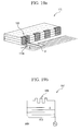
- FIG. 7 is a perspective view of a dielectric antenna.
- FIG. 8 is an exploded perspective view of the dielectric antenna shown in FIG. 7.
- FIG. 9a and FIG. 9b are an exploded plane view and an equivalent circuit diagram, respectively, in which a first substrate of the dielectric antenna shown in FIG. 7 is omitted.
- FIG. 10 is a schematic perspective view showing interrelations among elements of the dielectric antenna shown in FIG. 7.
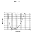
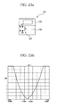
- FIG. 11 is a graphic chart representing VSWR characteristics of the dielectric antenna shown in FIG. 7.
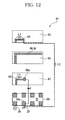
- FIG. 12 is an exploded plane view showing a dielectric antenna according to a first modification example of this embodiment.
- FIG. 13 is an equivalent circuit diagram of the dielectric antenna shown in FIG. 12.
- FIG. 14 is a graphic chart representing VSWR characteristics of the dielectric antenna shown in FIG. 12.
- FIG. 15a, and FIG. 15b and FIG. 15c are an equivalent circuit diagram and exploded plane views, respectively, showing a dielectric antenna according to a second modification example of this embodiment.
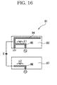
- FIG. 16 is an exploded plane view showing a dielectric antenna according to a third modification example of this embodiment.
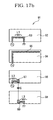
- FIG. 17a and FIG. 17b are an equivalent circuit diagram and an exploded plane view, respectively, showing a dielectric antenna according to a fourth modification example of this embodiment.
- FIG. 18b are a perspective view and an equivalent circuit diagram, respectively, of a dielectric antenna for a comparative experiment.
- FIG. 19a and FIG. 19b are a perspective view and an equivalent circuit diagram, respectively, of a dielectric antenna as a comparison object.
- FIG. 20 is a front view of a personal computer which is a communication device.
- An antenna matching circuit A1 shown in FIG. 1 is connected to an antenna (radiation element) A and includes a parallel resonant section 3.
- An inductance component L1 is connected to one side of the parallel resonant section 3, and an inductance component L2 and a capacitance component C which are connected in series are connected to the other side thereof.
- the antenna matching circuit A1 is an example of a case where the matching circuit according to the present invention is inserted in a feeder line, and it can be confirmed that a band of 1 GHz is obtained at a center frequency of 5 GHz by this configuration.
- the antenna A is a so-called inverted F type antenna, and the antenna matching circuit A1 is provided in the middle of a short end As of the antenna A.
- the antenna matching circuit A1 is applied to antennas other than the inverted F type antenna, for example, a monopole antenna (not shown), it can be connected to other positions appropriately.
- An antenna matching circuit A2 shown in FIG. 2 is a circuit similar to the aforementioned antenna matching circuit A1, but they are different in that the latter is provided in the feeder line, whereas the former is provided in a GND line. Also in the antenna matching circuit A2, as in the antenna matching circuit A1, a band of approximately 1 GHz can be obtained at a center frequency of 5 GHz.
- the parallel resonant section 3 included in the antenna matching circuit A3 is composed of an inductance component L1 and an inductance component L3 which are connected in series, and an inductance component L2 and a capacitance component C1 which are connected in series.
- Components other than the aforementioned components constituting the parallel resonant circuit, such as an inductance component L4 and a capacitance component C2 may be included.
- the resonant frequency is set at a relatively high frequency band of 5 GHz band in this embodiment, hence parasitic inductances La and Lb, and the like sometimes occur depending on circuit structure, and by performing structural design in which these parasitic inductances are reflected, it is possible to widen the band of the antenna.
- An antenna matching circuit A4 shown in FIG. 4 is an example in which one series resonant portion is further added to the aforementioned antenna matching circuit A2. Namely, an inductance component L1, an inductance component L2 and a capacitance component C1 which are connected in series, and an inductance component L3 and a capacitance component C2 which are connected in series are connected in parallel. Although not shown, another inductance component and another capacitance component which are connected in series may be further connected in parallel. It is within the scope of the present invention to provide plural series resonant portions as described just above.
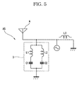
- An antenna matching circuit shown in FIG. 5 is an example of a case where a parallel resonant matching circuit is composed of two series resonant portions and an independent inductance component. Namely, an inductance component L1 and a capacitance component C1 which are connected in series, and an inductance component L2 and a capacitance component C2 which are also connected in series are connected in parallel, and an inductance component L3 is further connected in parallel with these components.
- the inductance component L3 is replaced with an inductance component included in a matching element of the antenna A which is an inverted F type antenna.
- another inductance component and another capacitance component which are connected in series may be further connected in parallel, and together with this or in place of this, another inductance component or another capacitance component may be connected in parallel.
- Such a configuration that plural series resonant portions are connected in parallel is also within the scope of the present invention.
- an antenna matching circuit A6 is an example of a case where a matching section according to the present invention spans both a feeder line and a GND line.
- a parallel resonant section 3 of the antenna matching circuit A6 is composed of an inductance component L1 and a capacitance component C which are connected in series on one side and an inductance component L2 and an inductance component L3 which are connected on the other side. Such a configuration is also possible.
- a dielectric antenna 10 including a radiation element and an antenna matching circuit as described later will be explained based on FIG. 7 and FIG. 8.
- the dielectric antenna 10 is formed by layering insulating substrates each made of a dielectric ceramic material, and includes a dielectric base 17 composed of five layers of a first substrate 11, a second substrate 12, a third substrate 13, a fourth substrate 14, and a fifth substrate 15 in order from the top down.
- a dielectric base 17 composed of five layers of a first substrate 11, a second substrate 12, a third substrate 13, a fourth substrate 14, and a fifth substrate 15 in order from the top down.
- Each of the substrates 11, 12, 13, 14, and 15 shown in FIG. 7 and FIG. 8 is represented by a single layer, but each substrate itself may be structured by layering thin substrates. Moreover, the thickness of each substrate may be different from that shown in the figures.
- All of the substrates 11, 12, 13, 14, and 15 are formed in a rectangle (quadrangle) having the same size when seen in plane view, and hence the dielectric base 17 formed by layering these substrates has a rectangular parallelepiped shape. Since there is no obstacle to the formation of the dielectric base 17 in shapes other than the rectangular parallelepiped shape, it is possible to form the dielectric base 17 in some other shape.
- An upper surface of the second substrate 12 (a surface facing a lower surface of the second substrate 11), an upper surface of the third substrate 13 (a surface facing a lower surface of the second substrate 12), an upper surface of the fourth substrate 14 (a surface facing a lower surface of the third substrate 13), and an upper surface of the fifth substrate 15 (a surface facing a lower surface of the fourth substrate 14) respectively constitute element forming surfaces 21, 31, 41, and 51 to form various kinds of elements.
- the dielectric base 17 is formed by a multi-layered body is to mechanically and electrically protect, by covering the element forming surface 21 of the second substrate 12 with the first substrate 11, an element and so on formed thereon. It is also possible to form the dielectric base 17 in a four-layer structure by omitting the first substrate 11 for some reason or by adopting some other method. It is further possible to omit the fifth substrate 15 if it is thought to be unnecessary. In contrast, it is also possible to further layer another layer substrate or other layer substrates (not shown) to form the dielectric base 17 in a six-layer or seven or more-layer structure.
- a capacitance component and an inductance component can be adjusted by making dielectric constants or magnetic permeabilities of members forming respective substrates different from each other or by interposing between substrates a substrate made of a member identical with or different from the substrates.
- the reason why the dielectric base 17 is formed in a rectangular parallelepiped shape is to allow the dielectric base to be easily produced by a multi-cavity molding by so-called dicer cutting or the like. It is needless to say that the dielectric base may be formed in other shapes.
- a dummy electrode for firmly soldering the dielectric antenna 10 onto a parent substrate (not shown) is provided on a rear surface of the fifth substrate 15.
- a power feeding terminal 19 formed on an end face of the dielectric base 17 is connected to a power feeding portion P of the parent substrate and a GND terminal 20 also formed on the end face of the dielectric base 17 is connected to a ground portion G thereof respectively by soldering.
- an antenna (radiation element) and an antenna matching circuit formed in the dielectric antenna 10 are as shown in FIG. 9a, and have the same structures as the antenna and the antenna matching circuit shown in FIG. 3. Accordingly, the same numerals and symbols as in FIG. 3 are used for the antenna and the antenna matching circuit shown in FIG. 9a.
- the parallel resonant section 3 included in the antenna matching circuit A3 is composed of the inductance component L1 and the inductance component L3 which are connected in series and the inductance component L2 and the capacitance component C1 which are connected in series.
- the inductance component L1 is formed by a first matching element 23 having an upside down U shape on the element forming surface 21 of the second substrate 12. One end of the first matching element 23 is connected to the power feeding terminal 19, and the other end thereof is connected to the GND terminal 20.
- a radiation element 33 having a substantially L shape is formed on the element forming surface 31 of the third substrate 13. The radiation element 33 constitutes the antenna A. One end of the radiation element 33 is open on the element forming surface 31, and a base end thereof is connected to the GND terminal 20.
- the inductance component L2 is formed by a second matching element 43 having a substantially L shape on the element forming surface 41 of the fourth substrate 14.
- a base end of the second matching element 43 is connected to the power feeding terminal 19, and an open end 43a thereof is formed wider than other portions.
- the reason why the open end 43a is formed wider is in order to adjust a capacitance component between the radiation element 33 and the open end 43a.
- the radiation element 33 and the second matching element 43 (open end 43a) form a capacitor structure via the third substrate 13 which is a dielectric, and the open end 43a is formed wider so that opposed areas of the radiation element 33 serving as one electrode of this capacitor structure and the second matching element 43 serving as the other electrode can be easily adjusted.
- the capacitance component C1 is formed by this capacitor structure.
- a rectangular GND element 53 is formed on the element forming surface 51 of the fifth substrate 15, and one end of this GND element 53 is connected to the GND terminal 20.
- the GND element 53 forms a capacitor structure with the open end 43a of the second matching element 43 with the fourth substrate 14 as a dielectric, and the capacitance component C2 is formed by this capacitor structure.
- the resonant frequency of the radiation element 33 is set at a relatively high frequency band of 5 GHz band, hence parasitic inductances La and Lb, and the like occur in the power feeding terminal 19, and by performing structural design in which these parasitic inductances are reflected, it is possible to widen the band of the antenna.
- the respective elements 23, 33, 43, and 53 may be formed by any method, but it is convenient to form them by a method of printing a conductive paste. This is because pattern printing is suitable for mass production, and besides variations in mass production can be reduced. It is also convenient to form the power feeding terminal 19 and the GND terminal 20 by the same method as above.
- VSWR characteristics when the aforementioned dielectric antenna 10 is formed by a dielectric base with dimensions of 5.0 x 2.0 x 0.8 mm and the resonant frequency is set to the 5 GHz band are as shown in FIG. 11 according to an electromagnetic field simulation.
- a band with the VSWR of 2 or less is 76 MHz at most according to the conventional means, a band of almost 1 GHz can be secured according to the dielectric antenna 10 although its theoretical basis is being elucidated now.
- a dielectric antenna 61 includes an antenna (radiation element) A and an antenna matching circuit A6.
- a parallel resonant section 3 included in the antenna matching circuit A6 is composed of an inductance component L1 and a capacitance component C which are connected in series and an inductance component L2 and an inductance component L3 which are connected in series.
- the inductance component L3 is formed by a first matching element 64 having an upside-down U shape on an element forming surface of a first substrate 63.
- One end of the first matching element 64 is connected to a power feeding terminal 29, and the other end thereof is connected to a GND terminal 30.
- a radiation element 66 having a substantially L shape is formed on an element forming surface of a second substrate 65.
- the radiation element 66 constitutes the antenna A.
- One end of the radiation element 66 is open on the element forming surface, and a base end thereof is connected to the power feeding terminal 29.
- the inductance component L2 is formed by the GND terminal 30.
- the inductance component L1 is formed by a second matching element 68 having a substantially L shape on an element forming surface of a third substrate 67.
- a base end of the second matching element 68 is connected to the power feeding terminal 29, and an open end 68a thereof is formed wider than other portions. The reason why the open end 68a is formed wider is in order to adjust a capacitance component between a GND element 70a and the open end 68a.
- the GND element 70a and the second matching element 68 form a capacitor structure via the third substrate 67 which is a dielectric, and the open end 68a is formed wider so that opposed areas of the GND element 70a serving as one electrode of this capacitor structure and the second matching element 68 serving as the other electrode can be easily adjusted.
- the capacitance component C is formed by this capacitor structure.
- a second modification example of this embodiment will be explained based on FIG. 15a to FIG. 15c.
- a dielectric antenna according to the second modification example can be regarded as one aspect of a case where the aforementioned antenna matching circuit A1 is incorporated into the dielectric antenna. This also applies to a third modification example described later.
- a capacitor structure using a second substrate 75 as a dielectric is formed by a second matching element 78 on a third substrate 77 and a radiation element 76 on a second substrate 75, and a series resonant portion is composed of a capacitance component C of this capacitor structure and an inductance component L2 of the second matching element 78.
- a first matching element 74 is formed on a first substrate 73, and a parallel resonant section is constructed by connecting an inductance component L1 of the first matching element 74 in parallel with the aforementioned series resonant portion.
- first matching element 74, the radiation element 76, and the second matching element 78 on separate dielectric layers of the first substrate 73, the second substrate 75, and the third substrate 77 makes it possible to enlarge occupied areas of the respective elements. If the occupied arrears can be enlarged, the values of the inductance component L1 and the inductance component L2 can be sufficiently large, which is beneficial in securing the degree of freedom of design, but it is also possible to form the respective elements on a single substrate. Incidentally, as shown in FIG.
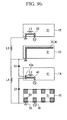
- a third modification example of this embodiment will be explained based on FIG. 16.
- a radiation element 84 and a first matching element 85 are both formed on a first substrate 83.
- a second matching element 88 is formed on a second substrate 87.
- any pattern can be formed on any substrate appropriately.
- FIG. 17a A fourth modification example of this embodiment will be explained based on FIG. 17a and FIG. 17b.
- a dielectric antenna 91 according to the fourth modification example as shown in FIG. 17a, an inductance component L1 is placed on one side of a parallel resonant section, and an inductance component L2, a capacitance component C, and an inductance component L3 which are connected in series are placed on the other side.
- a first matching element 96 which constitutes the inductance component L1 is formed on a first substrate 92 which constitutes the dielectric antenna 91, and a radiation element 95 is formed on a second substrate 94.
- a second matching element 97 which constitutes the inductance component L2 is formed on a third substrate 96, and a third matching element 99 which constitutes the inductance component L3 is formed on a fourth substrate 98.
- the second matching element 97 and the third matching element 99 form a capacitor structure with the third substrate 96 as a dielectric, and the capacitance component C is formed by this capacitor structure.
- dielectric antenna 91 an example of a case where a series resonant portion is constructed by providing the respective elements such as the second matching element 97 and the third matching element 99 on separate layers such as the third substrate 96 and the fourth substrate 98 and forming a capacitor structure by both the elements is shown, but irrespective of this construction, it is also possible to divide a pattern on one substrate and form a capacitor structure between the respective elements.
- FIG. 18a and FIG. 18b A dielectric antenna according to the present invention is shown in FIG. 18a and FIG. 18b, and a dielectric antenna as a comparison object is shown in FIG. 19a and FIG. 19b.
- a meander-shaped slit 103a and linear slits 103b, ... are formed in an end face terminal 103 of an dielectric antenna 101 shown in FIG. 18a so that an inductance component L and a capacitance component C occur as shown in FIG. 18b.
- a numeral 105 shown in FIG. 18b denotes a radiation element connected to the end face terminal 103.
- a meander-shaped slit 113a which is the same as the aforementioned slit 103a is formed in an end face terminal 113 of a dielectric antenna 111 shown in FIG. 19a and FIG. 19b.
- Such a linear slit as the slit 103b is not formed.
- a capacitance component C is formed in the end face terminal 113, but no inductance component is formed.
- An inductance component which can occur in the end face terminal 113 is only an inductance component due to parasitic.
- a numeral 115 shown in FIG. 19b denotes a radiation element connected to the end face terminal 113.
- the dielectric antenna 101 and the dielectric antenna 111 are compared in terms of bandwidth, at a frequency band of 5 GHz, the former can secure a bandwidth of approximately 1 GHz, whereas the latter can secure only 500 MHz. From this it turns out that an inductance component which constitutes an antenna matching circuit needs to be formed in a positive manner, and that an inductance component due to parasitic hardly contributes to an increase in bandwidth.
- a numeral 117 shown in FIG. 20 denotes a personal computer which functions as a communication device.
- the personal computer 117 is equipped with the aforementioned dielectric antenna, for example, the dielectric antenna 10, and it includes a power feeding means 119 for feeding power to the radiation element 33 (See FIG. 8) of the dielectric antenna 10.
- the dielectric antenna 10 can be used in a wide band of approximately 1 GHz, whereby the personal computer 117 can be used worldwide by making the power feeding means 119 itself usable in this band.
- the aforementioned dielectric antenna 10 or the like can be applied to others than this personal computer 117, and, for example, it can be suitably used for a cellular phone, a transceiver, and so on in addition to various kinds of PDAs (Personal Digital Aids).
- PDAs Personal Digital Aids
- antenna matching technology effective in widening the band can be provided. Accordingly, a single antenna enables good communication in a wide band.
Landscapes
- Details Of Aerials (AREA)
- Filters And Equalizers (AREA)
Applications Claiming Priority (2)
| Application Number | Priority Date | Filing Date | Title |
|---|---|---|---|
| JP2003127362A JP2004336250A (ja) | 2003-05-02 | 2003-05-02 | アンテナ整合回路、アンテナ整合回路を有する移動体通信装置、アンテナ整合回路を有する誘電体アンテナ |
| JP2003127362 | 2003-05-02 |
Publications (2)
| Publication Number | Publication Date |
|---|---|
| EP1475889A2 true EP1475889A2 (de) | 2004-11-10 |
| EP1475889A3 EP1475889A3 (de) | 2006-07-05 |
Family
ID=32985617
Family Applications (1)
| Application Number | Title | Priority Date | Filing Date |
|---|---|---|---|
| EP04252511A Withdrawn EP1475889A3 (de) | 2003-05-02 | 2004-04-29 | Antennenanpassungsschaltung, mobiles Kommunikationsgerät beinhaltend eine Antennenanpassungsschaltung, und dielektrische Antenne beinhaltend eine Antennenanpassungsschaltung |
Country Status (3)
| Country | Link |
|---|---|
| US (1) | US7088307B2 (de) |
| EP (1) | EP1475889A3 (de) |
| JP (1) | JP2004336250A (de) |
Cited By (10)
| Publication number | Priority date | Publication date | Assignee | Title |
|---|---|---|---|---|
| WO2008081077A1 (en) * | 2007-01-04 | 2008-07-10 | Pulse Finland Oy | Antenna structure |
| EP2056488A4 (de) * | 2006-10-27 | 2010-06-02 | Murata Manufacturing Co | Artikel mit elektromagnetisch gekoppeltem modul |
| CN101964441A (zh) * | 2009-07-24 | 2011-02-02 | 深圳富泰宏精密工业有限公司 | 天线组件、其制作方法及集成有该天线组件的壳体 |
| EP2375495A1 (de) * | 2006-01-19 | 2011-10-12 | Murata Manufacturing Co., Ltd. | Drahtlose integrierte Schaltung |
| US8078106B2 (en) | 2006-01-19 | 2011-12-13 | Murata Manufacturing Co., Ltd. | Wireless IC device and component for wireless IC device |
| US8095085B2 (en) | 2007-06-08 | 2012-01-10 | Arizona Board Of Regents For And On Behalf Of Arizona State University | Automatic antenna tuning unit for software-defined and cognitive radio |
| US8289219B2 (en) | 2007-05-02 | 2012-10-16 | Nokia Corporation | Antenna arrangement |
| US9030371B2 (en) | 2010-01-19 | 2015-05-12 | Murata Manufacturing Co., Ltd. | Antenna device and communication terminal apparatus |
| CN104836030A (zh) * | 2014-02-12 | 2015-08-12 | 宏碁股份有限公司 | 移动通信装置 |
| US9728851B2 (en) | 2013-10-02 | 2017-08-08 | Acer Incorporated | Mobile communication device |
Families Citing this family (139)
| Publication number | Priority date | Publication date | Assignee | Title |
|---|---|---|---|---|
| US7242364B2 (en) * | 2005-09-29 | 2007-07-10 | Nokia Corporation | Dual-resonant antenna |
| WO2007083575A1 (ja) * | 2006-01-19 | 2007-07-26 | Murata Manufacturing Co., Ltd. | 無線icデバイス |
| RU2378746C1 (ru) * | 2006-01-19 | 2010-01-10 | Мурата Мэньюфэкчуринг Ко., Лтд. | Беспроводное устройство на интегральной схеме и компонент беспроводного устройства на интегральной схеме |
| KR101050317B1 (ko) * | 2006-01-19 | 2011-07-19 | 가부시키가이샤 무라타 세이사쿠쇼 | 무선ic디바이스 및 무선ic디바이스용 부품 |
| WO2007122870A1 (ja) | 2006-04-10 | 2007-11-01 | Murata Manufacturing Co., Ltd. | 無線icデバイス |
| WO2007119304A1 (ja) | 2006-04-14 | 2007-10-25 | Murata Manufacturing Co., Ltd. | 無線icデバイス |
| RU2366045C1 (ru) * | 2006-04-14 | 2009-08-27 | Мурата Мэньюфэкчуринг Ко., Лтд. | Антенна |
| CN102780085A (zh) * | 2006-04-14 | 2012-11-14 | 株式会社村田制作所 | 天线 |
| US9064198B2 (en) | 2006-04-26 | 2015-06-23 | Murata Manufacturing Co., Ltd. | Electromagnetic-coupling-module-attached article |
| JP4803253B2 (ja) * | 2006-04-26 | 2011-10-26 | 株式会社村田製作所 | 給電回路基板付き物品 |
| DE112007001222B4 (de) | 2006-05-26 | 2017-10-05 | Murata Manufacturing Co., Ltd. | Datenkoppler |
| EP2023499A4 (de) * | 2006-05-30 | 2011-04-20 | Murata Manufacturing Co | Informationsendgerät |
| EP2023275B1 (de) | 2006-06-01 | 2011-04-27 | Murata Manufacturing Co. Ltd. | Hochfrequenz-ic-anordnung und zusammengesetzte komponente für eine hochfrequenz-ic-anordnung |
| WO2007145053A1 (ja) | 2006-06-12 | 2007-12-21 | Murata Manufacturing Co., Ltd. | 電磁結合モジュール、無線icデバイスの検査システム及びそれを用いた電磁結合モジュール、無線icデバイスの製造方法 |
| JP4281850B2 (ja) | 2006-06-30 | 2009-06-17 | 株式会社村田製作所 | 光ディスク |
| JP4957724B2 (ja) | 2006-07-11 | 2012-06-20 | 株式会社村田製作所 | アンテナ及び無線icデバイス |
| WO2008023636A1 (en) | 2006-08-24 | 2008-02-28 | Murata Manufacturing Co., Ltd. | Wireless ic device inspecting system and wireless ic device manufacturing method using the same |
| DE112007002024B4 (de) | 2006-09-26 | 2010-06-10 | Murata Mfg. Co., Ltd., Nagaokakyo-shi | Induktiv gekoppeltes Modul und Element mit induktiv gekoppeltem Modul |
| JP4844388B2 (ja) * | 2006-12-28 | 2011-12-28 | Tdk株式会社 | アンテナ装置 |
| WO2008090943A1 (ja) | 2007-01-26 | 2008-07-31 | Murata Manufacturing Co., Ltd. | 電磁結合モジュール付き容器 |
| WO2008096576A1 (ja) | 2007-02-06 | 2008-08-14 | Murata Manufacturing Co., Ltd. | 電磁結合モジュール付き包装材 |
| WO2008096574A1 (ja) * | 2007-02-06 | 2008-08-14 | Murata Manufacturing Co., Ltd. | 電磁結合モジュール付き包装材 |
| US8009101B2 (en) | 2007-04-06 | 2011-08-30 | Murata Manufacturing Co., Ltd. | Wireless IC device |
| JP5024372B2 (ja) | 2007-04-06 | 2012-09-12 | 株式会社村田製作所 | 無線icデバイス |
| WO2008126649A1 (ja) | 2007-04-09 | 2008-10-23 | Murata Manufacturing Co., Ltd. | 無線icデバイス |
| US8235299B2 (en) | 2007-07-04 | 2012-08-07 | Murata Manufacturing Co., Ltd. | Wireless IC device and component for wireless IC device |
| US7762472B2 (en) | 2007-07-04 | 2010-07-27 | Murata Manufacturing Co., Ltd | Wireless IC device |
| WO2008136226A1 (ja) | 2007-04-26 | 2008-11-13 | Murata Manufacturing Co., Ltd. | 無線icデバイス |
| JP4433097B2 (ja) * | 2007-04-27 | 2010-03-17 | 株式会社村田製作所 | 無線icデバイス |
| WO2008136220A1 (ja) * | 2007-04-27 | 2008-11-13 | Murata Manufacturing Co., Ltd. | 無線icデバイス |
| DE112008000065B4 (de) | 2007-05-10 | 2011-07-07 | Murata Manufacturing Co., Ltd., Kyoto-fu | Drahtloses IC-Bauelement |
| JP4666102B2 (ja) * | 2007-05-11 | 2011-04-06 | 株式会社村田製作所 | 無線icデバイス |
| WO2008149946A1 (ja) * | 2007-06-08 | 2008-12-11 | Murata Manufacturing Co., Ltd. | 無線icデバイス |
| WO2009001814A1 (ja) | 2007-06-27 | 2008-12-31 | Murata Manufacturing Co., Ltd. | 無線icデバイス |
| WO2009008296A1 (ja) | 2007-07-09 | 2009-01-15 | Murata Manufacturing Co., Ltd. | 無線icデバイス |
| CN104540317B (zh) | 2007-07-17 | 2018-11-02 | 株式会社村田制作所 | 印制布线基板 |
| JP4867831B2 (ja) * | 2007-07-18 | 2012-02-01 | 株式会社村田製作所 | 無線icデバイス |
| US20090021352A1 (en) | 2007-07-18 | 2009-01-22 | Murata Manufacturing Co., Ltd. | Radio frequency ic device and electronic apparatus |
| EP2086052B1 (de) * | 2007-07-18 | 2012-05-02 | Murata Manufacturing Co. Ltd. | Drahtloses ic-gerät |
| US7830311B2 (en) | 2007-07-18 | 2010-11-09 | Murata Manufacturing Co., Ltd. | Wireless IC device and electronic device |
| JP4434311B2 (ja) | 2007-07-18 | 2010-03-17 | 株式会社村田製作所 | 無線icデバイスおよびその製造方法 |
| JP5104865B2 (ja) | 2007-07-18 | 2012-12-19 | 株式会社村田製作所 | 無線icデバイス |
| JP4867830B2 (ja) * | 2007-07-18 | 2012-02-01 | 株式会社村田製作所 | 無線icデバイス |
| KR100891623B1 (ko) * | 2007-08-13 | 2009-04-02 | 주식회사 이엠따블유안테나 | 공진 주파수 가변형 안테나 |
| JP4605203B2 (ja) * | 2007-10-15 | 2011-01-05 | ソニー株式会社 | 通信システム並びに通信装置 |
| CN101595599B (zh) | 2007-12-20 | 2013-05-01 | 株式会社村田制作所 | 无线ic器件 |
| EP2557528A3 (de) | 2007-12-26 | 2017-01-18 | Murata Manufacturing Co., Ltd. | Antennenvorrichtung und drahtlose integrierte Schaltung |
| EP2251934B1 (de) | 2008-03-03 | 2018-05-02 | Murata Manufacturing Co. Ltd. | Drahtlose integrierte schaltung und drahtloses kommunikationssystem |
| JP4518211B2 (ja) | 2008-03-03 | 2010-08-04 | 株式会社村田製作所 | 複合アンテナ |
| JP4404166B2 (ja) | 2008-03-26 | 2010-01-27 | 株式会社村田製作所 | 無線icデバイス |
| JP4535209B2 (ja) | 2008-04-14 | 2010-09-01 | 株式会社村田製作所 | 無線icデバイス、電子機器及び無線icデバイスの共振周波数の調整方法 |
| CN103295056B (zh) | 2008-05-21 | 2016-12-28 | 株式会社村田制作所 | 无线ic器件 |
| WO2009142068A1 (ja) | 2008-05-22 | 2009-11-26 | 株式会社村田製作所 | 無線icデバイス及びその製造方法 |
| CN104077622B (zh) | 2008-05-26 | 2016-07-06 | 株式会社村田制作所 | 无线ic器件系统及无线ic器件的真伪判定方法 |
| EP2282372B1 (de) | 2008-05-28 | 2019-09-11 | Murata Manufacturing Co. Ltd. | Drahtlose ic-vorrichtung und bauteil für drahtlose ic-vorrichtung |
| JP4557186B2 (ja) | 2008-06-25 | 2010-10-06 | 株式会社村田製作所 | 無線icデバイスとその製造方法 |
| EP2306586B1 (de) | 2008-07-04 | 2014-04-02 | Murata Manufacturing Co. Ltd. | Drahtlose integrierte schaltung |
| WO2010021217A1 (ja) | 2008-08-19 | 2010-02-25 | 株式会社村田製作所 | 無線icデバイス及びその製造方法 |
| WO2010047214A1 (ja) | 2008-10-24 | 2010-04-29 | 株式会社村田製作所 | 無線icデバイス |
| DE112009002399B4 (de) | 2008-10-29 | 2022-08-18 | Murata Manufacturing Co., Ltd. | Funk-IC-Bauelement |
| DE112009002384B4 (de) | 2008-11-17 | 2021-05-06 | Murata Manufacturing Co., Ltd. | Antenne und Drahtlose-IC-Bauelement |
| CN102273012B (zh) | 2009-01-09 | 2013-11-20 | 株式会社村田制作所 | 无线ic器件及无线ic模块 |
| JP5041077B2 (ja) | 2009-01-16 | 2012-10-03 | 株式会社村田製作所 | 高周波デバイス及び無線icデバイス |
| EP2385580B1 (de) | 2009-01-30 | 2014-04-09 | Murata Manufacturing Co., Ltd. | Antenne und drahtlose ic-vorrichtung |
| CN102365828B (zh) * | 2009-03-31 | 2014-04-16 | 株式会社村田制作所 | 信号传输用通信体和耦合器 |
| JP5510450B2 (ja) | 2009-04-14 | 2014-06-04 | 株式会社村田製作所 | 無線icデバイス |
| EP2424041B1 (de) | 2009-04-21 | 2018-11-21 | Murata Manufacturing Co., Ltd. | Antennenvorrichtung und resonanzfrequenz-einstellverfahren dafür |
| WO2010140429A1 (ja) | 2009-06-03 | 2010-12-09 | 株式会社村田製作所 | 無線icデバイス及びその製造方法 |
| JP5516580B2 (ja) | 2009-06-19 | 2014-06-11 | 株式会社村田製作所 | 無線icデバイス及び給電回路と放射板との結合方法 |
| WO2011001709A1 (ja) | 2009-07-03 | 2011-01-06 | 株式会社村田製作所 | アンテナおよびアンテナモジュール |
| JP5182431B2 (ja) | 2009-09-28 | 2013-04-17 | 株式会社村田製作所 | 無線icデバイスおよびそれを用いた環境状態検出方法 |
| CN102577646B (zh) | 2009-09-30 | 2015-03-04 | 株式会社村田制作所 | 电路基板及其制造方法 |
| JP5304580B2 (ja) | 2009-10-02 | 2013-10-02 | 株式会社村田製作所 | 無線icデバイス |
| CN102576939B (zh) | 2009-10-16 | 2015-11-25 | 株式会社村田制作所 | 天线及无线ic器件 |
| JP5418600B2 (ja) | 2009-10-27 | 2014-02-19 | 株式会社村田製作所 | 送受信装置及び無線タグ読み取り装置 |
| CN102576930A (zh) | 2009-11-04 | 2012-07-11 | 株式会社村田制作所 | 通信终端及信息处理系统 |
| JP5327334B2 (ja) | 2009-11-04 | 2013-10-30 | 株式会社村田製作所 | 通信端末及び情報処理システム |
| WO2011055702A1 (ja) | 2009-11-04 | 2011-05-12 | 株式会社村田製作所 | 無線icタグ、リーダライタ及び情報処理システム |
| GB2487491B (en) | 2009-11-20 | 2014-09-03 | Murata Manufacturing Co | Antenna device and mobile communication terminal |
| EP2482379A4 (de) * | 2009-12-01 | 2014-04-09 | Murata Manufacturing Co | Antennenanpassungsvorrichtung, antennenvorrichtung und mobilkommunikationsendgerät |
| JP4978756B2 (ja) | 2009-12-24 | 2012-07-18 | 株式会社村田製作所 | 通信端末 |
| CN102474005B (zh) | 2010-01-19 | 2015-07-15 | 株式会社村田制作所 | 稳频电路、稳频器件、天线装置、及通信终端设备 |
| JP5652470B2 (ja) | 2010-03-03 | 2015-01-14 | 株式会社村田製作所 | 無線通信モジュール及び無線通信デバイス |
| WO2011108341A1 (ja) | 2010-03-03 | 2011-09-09 | 株式会社村田製作所 | 無線通信デバイス及び無線通信端末 |
| CN102576940B (zh) | 2010-03-12 | 2016-05-04 | 株式会社村田制作所 | 无线通信器件及金属制物品 |
| CN102668241B (zh) | 2010-03-24 | 2015-01-28 | 株式会社村田制作所 | Rfid系统 |
| JP5630499B2 (ja) | 2010-03-31 | 2014-11-26 | 株式会社村田製作所 | アンテナ装置及び無線通信デバイス |
| JP5299351B2 (ja) | 2010-05-14 | 2013-09-25 | 株式会社村田製作所 | 無線icデバイス |
| JP5170156B2 (ja) | 2010-05-14 | 2013-03-27 | 株式会社村田製作所 | 無線icデバイス |
| JP5376060B2 (ja) | 2010-07-08 | 2013-12-25 | 株式会社村田製作所 | アンテナ及びrfidデバイス |
| GB2495418B (en) | 2010-07-28 | 2017-05-24 | Murata Manufacturing Co | Antenna apparatus and communication terminal instrument |
| WO2012020748A1 (ja) | 2010-08-10 | 2012-02-16 | 株式会社村田製作所 | プリント配線板及び無線通信システム |
| CN102484497B (zh) * | 2010-08-11 | 2014-06-04 | 株式会社村田制作所 | 稳频电路、天线装置、及通信终端设备 |
| JP5234071B2 (ja) | 2010-09-03 | 2013-07-10 | 株式会社村田製作所 | Rficモジュール |
| CN103038939B (zh) | 2010-09-30 | 2015-11-25 | 株式会社村田制作所 | 无线ic器件 |
| CN105226382B (zh) | 2010-10-12 | 2019-06-11 | 株式会社村田制作所 | 天线装置及终端装置 |
| GB2501385B (en) | 2010-10-21 | 2015-05-27 | Murata Manufacturing Co | Communication terminal device |
| CN105048058B (zh) | 2011-01-05 | 2017-10-27 | 株式会社村田制作所 | 无线通信器件 |
| JP5304956B2 (ja) | 2011-01-14 | 2013-10-02 | 株式会社村田製作所 | Rfidチップパッケージ及びrfidタグ |
| CN103141031B (zh) | 2011-02-23 | 2015-05-20 | 株式会社村田制作所 | 阻抗变换电路以及通信终端装置 |
| CN104899639B (zh) | 2011-02-28 | 2018-08-07 | 株式会社村田制作所 | 无线通信器件 |
| JP5630566B2 (ja) | 2011-03-08 | 2014-11-26 | 株式会社村田製作所 | アンテナ装置及び通信端末機器 |
| JP5803190B2 (ja) * | 2011-03-23 | 2015-11-04 | 株式会社村田製作所 | アンテナ装置および通信端末装置 |
| JP5273326B2 (ja) | 2011-04-05 | 2013-08-28 | 株式会社村田製作所 | 無線通信デバイス |
| WO2012141070A1 (ja) | 2011-04-13 | 2012-10-18 | 株式会社村田製作所 | 無線icデバイス及び無線通信端末 |
| WO2012157596A1 (ja) | 2011-05-16 | 2012-11-22 | 株式会社村田製作所 | 無線icデバイス |
| WO2012165149A1 (ja) | 2011-05-31 | 2012-12-06 | 株式会社村田製作所 | アンテナ装置および通信端末装置 |
| WO2013008874A1 (ja) * | 2011-07-14 | 2013-01-17 | 株式会社村田製作所 | 無線通信デバイス |
| JP5333707B2 (ja) | 2011-07-15 | 2013-11-06 | 株式会社村田製作所 | 無線通信デバイス |
| WO2013011865A1 (ja) | 2011-07-19 | 2013-01-24 | 株式会社村田製作所 | アンテナモジュール、アンテナ装置、rfidタグおよび通信端末装置 |
| JP5418737B2 (ja) | 2011-09-09 | 2014-02-19 | 株式会社村田製作所 | アンテナ装置および無線デバイス |
| US9179492B2 (en) * | 2011-10-26 | 2015-11-03 | Texas Instruments Deutschland Gmbh | Electronic device, method and system for half duplex data transmission |
| CN103380432B (zh) | 2011-12-01 | 2016-10-19 | 株式会社村田制作所 | 无线ic器件及其制造方法 |
| JP5354137B1 (ja) | 2012-01-30 | 2013-11-27 | 株式会社村田製作所 | 無線icデバイス |
| JP5838846B2 (ja) * | 2012-02-17 | 2016-01-06 | 株式会社村田製作所 | インピーダンス変換素子および通信端末装置 |
| WO2013125610A1 (ja) | 2012-02-24 | 2013-08-29 | 株式会社村田製作所 | アンテナ装置および無線通信装置 |
| WO2013153697A1 (ja) | 2012-04-13 | 2013-10-17 | 株式会社村田製作所 | Rfidタグの検査方法及び検査装置 |
| JP5762377B2 (ja) | 2012-09-28 | 2015-08-12 | 太陽誘電株式会社 | インピーダンス整合回路およびアンテナシステム |
| JP2014116883A (ja) * | 2012-12-12 | 2014-06-26 | Sony Corp | アンテナ装置並びに通信装置 |
| US9287629B2 (en) | 2013-03-15 | 2016-03-15 | Murata Manufacturing Co., Ltd. | Impedance conversion device, antenna device and communication terminal device |
| TWI577081B (zh) * | 2013-04-24 | 2017-04-01 | 宏碁股份有限公司 | 行動裝置 |
| WO2017130348A1 (ja) | 2016-01-28 | 2017-08-03 | 富士通株式会社 | アンテナ装置 |
| CN209168856U (zh) * | 2016-07-15 | 2019-07-26 | 株式会社村田制作所 | 高频变压器以及移相器 |
| US11764473B2 (en) | 2016-08-29 | 2023-09-19 | Silicon Laboratories Inc. | Apparatus with partitioned radio frequency antenna and matching network and associated methods |
| US11749893B2 (en) | 2016-08-29 | 2023-09-05 | Silicon Laboratories Inc. | Apparatus for antenna impedance-matching and associated methods |
| US11769949B2 (en) | 2016-08-29 | 2023-09-26 | Silicon Laboratories Inc. | Apparatus with partitioned radio frequency antenna and matching network and associated methods |
| US11764749B2 (en) | 2016-08-29 | 2023-09-19 | Silicon Laboratories Inc. | Apparatus with partitioned radio frequency antenna and matching network and associated methods |
| US11894622B2 (en) * | 2016-08-29 | 2024-02-06 | Silicon Laboratories Inc. | Antenna structure with double-slotted loop and associated methods |
| CN110710119B (zh) | 2017-06-08 | 2021-07-27 | 株式会社村田制作所 | 高频模块 |
| US11894826B2 (en) | 2017-12-18 | 2024-02-06 | Silicon Laboratories Inc. | Radio-frequency apparatus with multi-band balun and associated methods |
| US11894621B2 (en) | 2017-12-18 | 2024-02-06 | Silicon Laboratories Inc. | Radio-frequency apparatus with multi-band balun with improved performance and associated methods |
| US11750167B2 (en) | 2017-11-27 | 2023-09-05 | Silicon Laboratories Inc. | Apparatus for radio-frequency matching networks and associated methods |
| US11916514B2 (en) | 2017-11-27 | 2024-02-27 | Silicon Laboratories Inc. | Radio-frequency apparatus with multi-band wideband balun and associated methods |
| WO2019160139A1 (ja) * | 2018-02-19 | 2019-08-22 | 株式会社村田製作所 | 多層基板、ローパスフィルタ、ハイパスフィルタ、マルチプレクサ、高周波フロントエンド回路、及び通信装置 |
| CN215989212U (zh) * | 2020-01-28 | 2022-03-08 | 株式会社村田制作所 | 天线装置及电子设备 |
| US11862872B2 (en) | 2021-09-30 | 2024-01-02 | Silicon Laboratories Inc. | Apparatus for antenna optimization and associated methods |
| TWI793867B (zh) * | 2021-11-19 | 2023-02-21 | 啓碁科技股份有限公司 | 通訊裝置 |
| CN117941254A (zh) | 2021-11-22 | 2024-04-26 | 株式会社村田制作所 | 滤波器装置、天线装置以及天线模块 |
| CN116207483A (zh) * | 2021-12-01 | 2023-06-02 | 启碁科技股份有限公司 | 通信装置 |
Family Cites Families (15)
| Publication number | Priority date | Publication date | Assignee | Title |
|---|---|---|---|---|
| US4145693A (en) * | 1977-03-17 | 1979-03-20 | Electrospace Systems, Inc. | Three band monopole antenna |
| US4141016A (en) | 1977-04-25 | 1979-02-20 | Antenna, Incorporated | AM-FM-CB Disguised antenna system |
| DE68922797T2 (de) * | 1988-07-14 | 1996-02-08 | Asahi Glass Co Ltd | Kraftfahrzeugantenne. |
| JPH05327331A (ja) | 1992-05-15 | 1993-12-10 | Matsushita Electric Works Ltd | プリントアンテナ |
| JP2822825B2 (ja) * | 1992-12-26 | 1998-11-11 | 株式会社村田製作所 | 複合電子部品 |
| JPH07321550A (ja) * | 1994-05-20 | 1995-12-08 | Murata Mfg Co Ltd | アンテナ装置 |
| JPH08148960A (ja) * | 1994-11-25 | 1996-06-07 | Oki Electric Ind Co Ltd | アンテナ整合回路 |
| US6329886B1 (en) | 1998-05-12 | 2001-12-11 | Nec Corporation | Impedance-matching method and circuit at different frequences |
| US6081242A (en) * | 1998-06-16 | 2000-06-27 | Galtronics U.S.A., Inc. | Antenna matching circuit |
| JP3889179B2 (ja) | 1999-03-29 | 2007-03-07 | 日本碍子株式会社 | アンテナ装置 |
| JP3708382B2 (ja) * | 1999-10-12 | 2005-10-19 | 日本碍子株式会社 | アンテナ装置 |
| JP2002026624A (ja) * | 2000-07-07 | 2002-01-25 | Nippon Tungsten Co Ltd | 誘電体アンテナモジュール |
| JP2002076750A (ja) * | 2000-08-24 | 2002-03-15 | Murata Mfg Co Ltd | アンテナ装置およびそれを備えた無線機 |
| US6577155B2 (en) | 2001-07-30 | 2003-06-10 | Fischer Custom Communications, Inc. | Apparatus and method for impedance control |
| KR100979581B1 (ko) * | 2002-01-31 | 2010-09-01 | 엔엑스피 비 브이 | 신호 처리 방법, 송신기 및 수신기 모듈, 기판 및 가전 제품 |
-
2003
- 2003-05-02 JP JP2003127362A patent/JP2004336250A/ja active Pending
-
2004
- 2004-04-23 US US10/831,464 patent/US7088307B2/en not_active Expired - Fee Related
- 2004-04-29 EP EP04252511A patent/EP1475889A3/de not_active Withdrawn
Cited By (12)
| Publication number | Priority date | Publication date | Assignee | Title |
|---|---|---|---|---|
| EP2375495A1 (de) * | 2006-01-19 | 2011-10-12 | Murata Manufacturing Co., Ltd. | Drahtlose integrierte Schaltung |
| US8078106B2 (en) | 2006-01-19 | 2011-12-13 | Murata Manufacturing Co., Ltd. | Wireless IC device and component for wireless IC device |
| US8326223B2 (en) | 2006-01-19 | 2012-12-04 | Murata Manufacturing Co., Ltd. | Wireless IC device and component for wireless IC device |
| EP2056488A4 (de) * | 2006-10-27 | 2010-06-02 | Murata Manufacturing Co | Artikel mit elektromagnetisch gekoppeltem modul |
| WO2008081077A1 (en) * | 2007-01-04 | 2008-07-10 | Pulse Finland Oy | Antenna structure |
| US8289219B2 (en) | 2007-05-02 | 2012-10-16 | Nokia Corporation | Antenna arrangement |
| US8095085B2 (en) | 2007-06-08 | 2012-01-10 | Arizona Board Of Regents For And On Behalf Of Arizona State University | Automatic antenna tuning unit for software-defined and cognitive radio |
| CN101964441A (zh) * | 2009-07-24 | 2011-02-02 | 深圳富泰宏精密工业有限公司 | 天线组件、其制作方法及集成有该天线组件的壳体 |
| US9030371B2 (en) | 2010-01-19 | 2015-05-12 | Murata Manufacturing Co., Ltd. | Antenna device and communication terminal apparatus |
| US9728851B2 (en) | 2013-10-02 | 2017-08-08 | Acer Incorporated | Mobile communication device |
| CN104836030A (zh) * | 2014-02-12 | 2015-08-12 | 宏碁股份有限公司 | 移动通信装置 |
| CN104836030B (zh) * | 2014-02-12 | 2019-01-22 | 宏碁股份有限公司 | 移动通信装置 |
Also Published As
| Publication number | Publication date |
|---|---|
| JP2004336250A (ja) | 2004-11-25 |
| EP1475889A3 (de) | 2006-07-05 |
| US7088307B2 (en) | 2006-08-08 |
| US20040217915A1 (en) | 2004-11-04 |
Similar Documents
| Publication | Publication Date | Title |
|---|---|---|
| US7088307B2 (en) | Antenna matching circuit, mobile communication device including antenna matching circuit, and dielectric antenna including antenna matching circuit | |
| US11139574B2 (en) | Antennaless wireless device | |
| US20220077581A1 (en) | Antennaless Wireless Device | |
| JP4423809B2 (ja) | 複共振アンテナ | |
| JP3180683B2 (ja) | 表面実装型アンテナ | |
| JP4089680B2 (ja) | アンテナ装置 | |
| US7663551B2 (en) | Multiband antenna apparatus and methods | |
| JP4189306B2 (ja) | 誘電体アンテナおよびそれを用いた通信機能を有する電気機器 | |
| US7786940B2 (en) | Antenna structure and wireless communication device including the same | |
| CN100375334C (zh) | 天线装置 | |
| US20120280890A1 (en) | Antenna and wireless communication device | |
| WO2003047025A1 (en) | Dual-band antenna arrangement | |
| JP2004088218A (ja) | 平面アンテナ | |
| KR20050085045A (ko) | 칩 안테나, 칩 안테나 유닛 및 그것들을 사용하는 무선통신 장치 | |
| CN113764866A (zh) | 一种天线装置、电子设备 | |
| CN103299483B (zh) | 天线装置用基板及天线装置 | |
| JP4073789B2 (ja) | 誘電体アンテナ及びそれを内蔵する移動体通信機 | |
| JPH10173425A (ja) | 表面実装型アンテナ、アンテナ装置および通信機 | |
| CN113497345A (zh) | 天线结构和电子设备 | |
| JP2011061638A (ja) | アンテナ装置 | |
| JP2003258547A (ja) | アンテナ装置 | |
| JP3878556B2 (ja) | 誘電体アンテナ及びそれを内蔵する移動体通信機 | |
| US7728773B2 (en) | Multi-band antenna | |
| US20240030610A2 (en) | Monopole wire-patch antenna with enlarged bandwidth | |
| JP2003273628A (ja) | 誘電体アンテナ |
Legal Events
| Date | Code | Title | Description |
|---|---|---|---|
| PUAI | Public reference made under article 153(3) epc to a published international application that has entered the european phase |
Free format text: ORIGINAL CODE: 0009012 |
|
| AK | Designated contracting states |
Kind code of ref document: A2 Designated state(s): AT BE BG CH CY CZ DE DK EE ES FI FR GB GR HU IE IT LI LU MC NL PL PT RO SE SI SK TR |
|
| AX | Request for extension of the european patent |
Extension state: AL HR LT LV MK |
|
| PUAL | Search report despatched |
Free format text: ORIGINAL CODE: 0009013 |
|
| AK | Designated contracting states |
Kind code of ref document: A3 Designated state(s): AT BE BG CH CY CZ DE DK EE ES FI FR GB GR HU IE IT LI LU MC NL PL PT RO SE SI SK TR |
|
| AX | Request for extension of the european patent |
Extension state: AL HR LT LV MK |
|
| RIC1 | Information provided on ipc code assigned before grant |
Ipc: H01Q 23/00 20060101ALI20060529BHEP Ipc: H03H 7/38 20060101AFI20040817BHEP |
|
| AKX | Designation fees paid | ||
| STAA | Information on the status of an ep patent application or granted ep patent |
Free format text: STATUS: THE APPLICATION IS DEEMED TO BE WITHDRAWN |
|
| REG | Reference to a national code |
Ref country code: DE Ref legal event code: 8566 |
|
| 18D | Application deemed to be withdrawn |
Effective date: 20061102 |