EP1445095A1 - Substrat de support a film mince composite, substrat de support a film conducteur transparent et corps emetteur pour eclairage de panneau - Google Patents
Substrat de support a film mince composite, substrat de support a film conducteur transparent et corps emetteur pour eclairage de panneau Download PDFInfo
- Publication number
- EP1445095A1 EP1445095A1 EP02775391A EP02775391A EP1445095A1 EP 1445095 A1 EP1445095 A1 EP 1445095A1 EP 02775391 A EP02775391 A EP 02775391A EP 02775391 A EP02775391 A EP 02775391A EP 1445095 A1 EP1445095 A1 EP 1445095A1
- Authority
- EP
- European Patent Office
- Prior art keywords
- thin film
- composite thin
- refractive index
- binder
- filler
- Prior art date
- Legal status (The legal status is an assumption and is not a legal conclusion. Google has not performed a legal analysis and makes no representation as to the accuracy of the status listed.)
- Granted
Links
- 239000002131 composite material Substances 0.000 title claims abstract description 309
- 239000000758 substrate Substances 0.000 title claims abstract description 308
- 239000010409 thin film Substances 0.000 title claims abstract description 251
- 239000010408 film Substances 0.000 title claims description 107
- 239000000945 filler Substances 0.000 claims abstract description 200
- 239000011230 binding agent Substances 0.000 claims abstract description 167
- VYPSYNLAJGMNEJ-UHFFFAOYSA-N Silicium dioxide Chemical compound O=[Si]=O VYPSYNLAJGMNEJ-UHFFFAOYSA-N 0.000 claims description 181
- 239000000463 material Substances 0.000 claims description 118
- 239000002245 particle Substances 0.000 claims description 85
- 239000010419 fine particle Substances 0.000 claims description 76
- 239000000377 silicon dioxide Substances 0.000 claims description 67
- 238000000576 coating method Methods 0.000 claims description 54
- 239000011248 coating agent Substances 0.000 claims description 50
- 239000000203 mixture Substances 0.000 claims description 50
- 150000004706 metal oxides Chemical class 0.000 claims description 38
- 229910044991 metal oxide Inorganic materials 0.000 claims description 37
- 229920001296 polysiloxane Polymers 0.000 claims description 37
- 229920000620 organic polymer Polymers 0.000 claims description 36
- 239000011148 porous material Substances 0.000 claims description 28
- 239000004964 aerogel Substances 0.000 claims description 23
- 238000001035 drying Methods 0.000 claims description 23
- 229920000642 polymer Polymers 0.000 claims description 23
- 229910052751 metal Inorganic materials 0.000 claims description 19
- 239000002184 metal Substances 0.000 claims description 19
- 150000002736 metal compounds Chemical class 0.000 claims description 3
- 239000010410 layer Substances 0.000 description 89
- 239000004965 Silica aerogel Substances 0.000 description 25
- OKKJLVBELUTLKV-UHFFFAOYSA-N Methanol Chemical compound OC OKKJLVBELUTLKV-UHFFFAOYSA-N 0.000 description 24
- 238000000034 method Methods 0.000 description 23
- GWEVSGVZZGPLCZ-UHFFFAOYSA-N Titan oxide Chemical compound O=[Ti]=O GWEVSGVZZGPLCZ-UHFFFAOYSA-N 0.000 description 22
- -1 alkoxy silane Chemical compound 0.000 description 21
- 150000001875 compounds Chemical class 0.000 description 21
- 239000002904 solvent Substances 0.000 description 21
- 230000005484 gravity Effects 0.000 description 18
- 230000000052 comparative effect Effects 0.000 description 17
- 230000000694 effects Effects 0.000 description 17
- 239000011800 void material Substances 0.000 description 15
- CURLTUGMZLYLDI-UHFFFAOYSA-N Carbon dioxide Chemical compound O=C=O CURLTUGMZLYLDI-UHFFFAOYSA-N 0.000 description 14
- 239000011521 glass Substances 0.000 description 14
- 230000008569 process Effects 0.000 description 14
- 239000007787 solid Substances 0.000 description 14
- LFQSCWFLJHTTHZ-UHFFFAOYSA-N Ethanol Chemical compound CCO LFQSCWFLJHTTHZ-UHFFFAOYSA-N 0.000 description 13
- KFZMGEQAYNKOFK-UHFFFAOYSA-N Isopropanol Chemical compound CC(C)O KFZMGEQAYNKOFK-UHFFFAOYSA-N 0.000 description 13
- 125000003545 alkoxy group Chemical group 0.000 description 12
- 239000000047 product Substances 0.000 description 12
- 239000007788 liquid Substances 0.000 description 11
- 239000011240 wet gel Substances 0.000 description 11
- 239000011247 coating layer Substances 0.000 description 10
- 239000004793 Polystyrene Substances 0.000 description 9
- 238000010438 heat treatment Methods 0.000 description 9
- 229920002223 polystyrene Polymers 0.000 description 9
- 239000000126 substance Substances 0.000 description 9
- 125000001424 substituent group Chemical group 0.000 description 9
- 239000003570 air Substances 0.000 description 8
- 239000002609 medium Substances 0.000 description 8
- 238000002156 mixing Methods 0.000 description 8
- 239000000243 solution Substances 0.000 description 8
- 230000005540 biological transmission Effects 0.000 description 7
- 239000001569 carbon dioxide Substances 0.000 description 7
- 229910002092 carbon dioxide Inorganic materials 0.000 description 7
- 239000007789 gas Substances 0.000 description 7
- 125000002887 hydroxy group Chemical group [H]O* 0.000 description 7
- YCKRFDGAMUMZLT-UHFFFAOYSA-N Fluorine atom Chemical compound [F] YCKRFDGAMUMZLT-UHFFFAOYSA-N 0.000 description 6
- YXFVVABEGXRONW-UHFFFAOYSA-N Toluene Chemical compound CC1=CC=CC=C1 YXFVVABEGXRONW-UHFFFAOYSA-N 0.000 description 6
- 239000012080 ambient air Substances 0.000 description 6
- 230000007423 decrease Effects 0.000 description 6
- 229910052731 fluorine Inorganic materials 0.000 description 6
- 239000011737 fluorine Substances 0.000 description 6
- 229910052809 inorganic oxide Inorganic materials 0.000 description 6
- 229920000058 polyacrylate Polymers 0.000 description 6
- 229910000077 silane Inorganic materials 0.000 description 6
- MCMNRKCIXSYSNV-UHFFFAOYSA-N Zirconium dioxide Chemical compound O=[Zr]=O MCMNRKCIXSYSNV-UHFFFAOYSA-N 0.000 description 5
- 239000000499 gel Substances 0.000 description 5
- 230000003301 hydrolyzing effect Effects 0.000 description 5
- 229960004592 isopropanol Drugs 0.000 description 5
- 239000000178 monomer Substances 0.000 description 5
- 239000002243 precursor Substances 0.000 description 5
- 238000000352 supercritical drying Methods 0.000 description 5
- 239000002344 surface layer Substances 0.000 description 5
- 238000001947 vapour-phase growth Methods 0.000 description 5
- XLYOFNOQVPJJNP-UHFFFAOYSA-N water Substances O XLYOFNOQVPJJNP-UHFFFAOYSA-N 0.000 description 5
- LYCAIKOWRPUZTN-UHFFFAOYSA-N Ethylene glycol Chemical class OCCO LYCAIKOWRPUZTN-UHFFFAOYSA-N 0.000 description 4
- 239000004890 Hydrophobing Agent Substances 0.000 description 4
- PPBRXRYQALVLMV-UHFFFAOYSA-N Styrene Chemical compound C=CC1=CC=CC=C1 PPBRXRYQALVLMV-UHFFFAOYSA-N 0.000 description 4
- BOTDANWDWHJENH-UHFFFAOYSA-N Tetraethyl orthosilicate Chemical compound CCO[Si](OCC)(OCC)OCC BOTDANWDWHJENH-UHFFFAOYSA-N 0.000 description 4
- PNEYBMLMFCGWSK-UHFFFAOYSA-N aluminium oxide Inorganic materials [O-2].[O-2].[O-2].[Al+3].[Al+3] PNEYBMLMFCGWSK-UHFFFAOYSA-N 0.000 description 4
- MTHSVFCYNBDYFN-UHFFFAOYSA-N diethylene glycol Chemical class OCCOCCO MTHSVFCYNBDYFN-UHFFFAOYSA-N 0.000 description 4
- 230000006872 improvement Effects 0.000 description 4
- 238000005259 measurement Methods 0.000 description 4
- 238000012545 processing Methods 0.000 description 4
- 229920002050 silicone resin Polymers 0.000 description 4
- 239000007858 starting material Substances 0.000 description 4
- TVIVIEFSHFOWTE-UHFFFAOYSA-K tri(quinolin-8-yloxy)alumane Chemical compound [Al+3].C1=CN=C2C([O-])=CC=CC2=C1.C1=CN=C2C([O-])=CC=CC2=C1.C1=CN=C2C([O-])=CC=CC2=C1 TVIVIEFSHFOWTE-UHFFFAOYSA-K 0.000 description 4
- ZWEHNKRNPOVVGH-UHFFFAOYSA-N 2-Butanone Chemical compound CCC(C)=O ZWEHNKRNPOVVGH-UHFFFAOYSA-N 0.000 description 3
- UHOVQNZJYSORNB-UHFFFAOYSA-N Benzene Chemical compound C1=CC=CC=C1 UHOVQNZJYSORNB-UHFFFAOYSA-N 0.000 description 3
- 239000004593 Epoxy Substances 0.000 description 3
- ZMXDDKWLCZADIW-UHFFFAOYSA-N N,N-Dimethylformamide Chemical compound CN(C)C=O ZMXDDKWLCZADIW-UHFFFAOYSA-N 0.000 description 3
- 239000004115 Sodium Silicate Substances 0.000 description 3
- 125000004432 carbon atom Chemical group C* 0.000 description 3
- 239000003795 chemical substances by application Substances 0.000 description 3
- 239000008199 coating composition Substances 0.000 description 3
- 239000007771 core particle Substances 0.000 description 3
- 239000006185 dispersion Substances 0.000 description 3
- 239000002612 dispersion medium Substances 0.000 description 3
- 230000003287 optical effect Effects 0.000 description 3
- 238000012643 polycondensation polymerization Methods 0.000 description 3
- 239000002861 polymer material Substances 0.000 description 3
- 239000011164 primary particle Substances 0.000 description 3
- 238000010298 pulverizing process Methods 0.000 description 3
- 229910052710 silicon Inorganic materials 0.000 description 3
- NTHWMYGWWRZVTN-UHFFFAOYSA-N sodium silicate Chemical compound [Na+].[Na+].[O-][Si]([O-])=O NTHWMYGWWRZVTN-UHFFFAOYSA-N 0.000 description 3
- 229910052911 sodium silicate Inorganic materials 0.000 description 3
- XOLBLPGZBRYERU-UHFFFAOYSA-N tin dioxide Chemical compound O=[Sn]=O XOLBLPGZBRYERU-UHFFFAOYSA-N 0.000 description 3
- 238000001771 vacuum deposition Methods 0.000 description 3
- 229920000178 Acrylic resin Polymers 0.000 description 2
- 239000004925 Acrylic resin Substances 0.000 description 2
- QGZKDVFQNNGYKY-UHFFFAOYSA-N Ammonia Chemical compound N QGZKDVFQNNGYKY-UHFFFAOYSA-N 0.000 description 2
- VEXZGXHMUGYJMC-UHFFFAOYSA-N Hydrochloric acid Chemical compound Cl VEXZGXHMUGYJMC-UHFFFAOYSA-N 0.000 description 2
- CTQNGGLPUBDAKN-UHFFFAOYSA-N O-Xylene Chemical compound CC1=CC=CC=C1C CTQNGGLPUBDAKN-UHFFFAOYSA-N 0.000 description 2
- XUIMIQQOPSSXEZ-UHFFFAOYSA-N Silicon Chemical group [Si] XUIMIQQOPSSXEZ-UHFFFAOYSA-N 0.000 description 2
- 239000007983 Tris buffer Substances 0.000 description 2
- XLOMVQKBTHCTTD-UHFFFAOYSA-N Zinc monoxide Chemical compound [Zn]=O XLOMVQKBTHCTTD-UHFFFAOYSA-N 0.000 description 2
- 229910052782 aluminium Inorganic materials 0.000 description 2
- XAGFODPZIPBFFR-UHFFFAOYSA-N aluminium Chemical compound [Al] XAGFODPZIPBFFR-UHFFFAOYSA-N 0.000 description 2
- 238000000149 argon plasma sintering Methods 0.000 description 2
- 230000015572 biosynthetic process Effects 0.000 description 2
- 230000008859 change Effects 0.000 description 2
- 229910052681 coesite Inorganic materials 0.000 description 2
- 229920001940 conductive polymer Polymers 0.000 description 2
- 229910052906 cristobalite Inorganic materials 0.000 description 2
- 238000009792 diffusion process Methods 0.000 description 2
- 238000010894 electron beam technology Methods 0.000 description 2
- 238000005227 gel permeation chromatography Methods 0.000 description 2
- 238000001879 gelation Methods 0.000 description 2
- FFUAGWLWBBFQJT-UHFFFAOYSA-N hexamethyldisilazane Chemical compound C[Si](C)(C)N[Si](C)(C)C FFUAGWLWBBFQJT-UHFFFAOYSA-N 0.000 description 2
- UQEAIHBTYFGYIE-UHFFFAOYSA-N hexamethyldisiloxane Chemical compound C[Si](C)(C)O[Si](C)(C)C UQEAIHBTYFGYIE-UHFFFAOYSA-N 0.000 description 2
- 150000002430 hydrocarbons Chemical group 0.000 description 2
- 230000007062 hydrolysis Effects 0.000 description 2
- 238000006460 hydrolysis reaction Methods 0.000 description 2
- AMGQUBHHOARCQH-UHFFFAOYSA-N indium;oxotin Chemical compound [In].[Sn]=O AMGQUBHHOARCQH-UHFFFAOYSA-N 0.000 description 2
- MRNHPUHPBOKKQT-UHFFFAOYSA-N indium;tin;hydrate Chemical compound O.[In].[Sn] MRNHPUHPBOKKQT-UHFFFAOYSA-N 0.000 description 2
- 238000004519 manufacturing process Methods 0.000 description 2
- JKQOBWVOAYFWKG-UHFFFAOYSA-N molybdenum trioxide Chemical compound O=[Mo](=O)=O JKQOBWVOAYFWKG-UHFFFAOYSA-N 0.000 description 2
- 125000005375 organosiloxane group Chemical group 0.000 description 2
- 238000005268 plasma chemical vapour deposition Methods 0.000 description 2
- 239000002985 plastic film Substances 0.000 description 2
- 229920006255 plastic film Polymers 0.000 description 2
- 238000006116 polymerization reaction Methods 0.000 description 2
- 238000002360 preparation method Methods 0.000 description 2
- 238000001552 radio frequency sputter deposition Methods 0.000 description 2
- 229920005989 resin Polymers 0.000 description 2
- 239000011347 resin Substances 0.000 description 2
- 125000005372 silanol group Chemical group 0.000 description 2
- 239000010703 silicon Substances 0.000 description 2
- 239000002356 single layer Substances 0.000 description 2
- 238000004528 spin coating Methods 0.000 description 2
- 238000004544 sputter deposition Methods 0.000 description 2
- 229910052682 stishovite Inorganic materials 0.000 description 2
- 238000010557 suspension polymerization reaction Methods 0.000 description 2
- DLYUQMMRRRQYAE-UHFFFAOYSA-N tetraphosphorus decaoxide Chemical compound O1P(O2)(=O)OP3(=O)OP1(=O)OP2(=O)O3 DLYUQMMRRRQYAE-UHFFFAOYSA-N 0.000 description 2
- 229910052905 tridymite Inorganic materials 0.000 description 2
- 239000008096 xylene Substances 0.000 description 2
- 239000011787 zinc oxide Substances 0.000 description 2
- POAOYUHQDCAZBD-UHFFFAOYSA-N 2-butoxyethanol Chemical compound CCCCOCCO POAOYUHQDCAZBD-UHFFFAOYSA-N 0.000 description 1
- SVONRAPFKPVNKG-UHFFFAOYSA-N 2-ethoxyethyl acetate Chemical compound CCOCCOC(C)=O SVONRAPFKPVNKG-UHFFFAOYSA-N 0.000 description 1
- 229910011255 B2O3 Inorganic materials 0.000 description 1
- 239000004215 Carbon black (E152) Substances 0.000 description 1
- ZAMOUSCENKQFHK-UHFFFAOYSA-N Chlorine atom Chemical compound [Cl] ZAMOUSCENKQFHK-UHFFFAOYSA-N 0.000 description 1
- 229910001111 Fine metal Inorganic materials 0.000 description 1
- 230000005355 Hall effect Effects 0.000 description 1
- 229920000877 Melamine resin Polymers 0.000 description 1
- VVQNEPGJFQJSBK-UHFFFAOYSA-N Methyl methacrylate Chemical compound COC(=O)C(C)=C VVQNEPGJFQJSBK-UHFFFAOYSA-N 0.000 description 1
- 229910052581 Si3N4 Inorganic materials 0.000 description 1
- 229910020381 SiO1.5 Inorganic materials 0.000 description 1
- BLRPTPMANUNPDV-UHFFFAOYSA-N Silane Chemical compound [SiH4] BLRPTPMANUNPDV-UHFFFAOYSA-N 0.000 description 1
- 239000006087 Silane Coupling Agent Substances 0.000 description 1
- 229910003076 TiO2-Al2O3 Inorganic materials 0.000 description 1
- 150000004703 alkoxides Chemical class 0.000 description 1
- 229910021529 ammonia Inorganic materials 0.000 description 1
- GHPGOEFPKIHBNM-UHFFFAOYSA-N antimony(3+);oxygen(2-) Chemical compound [O-2].[O-2].[O-2].[Sb+3].[Sb+3] GHPGOEFPKIHBNM-UHFFFAOYSA-N 0.000 description 1
- 230000000903 blocking effect Effects 0.000 description 1
- 238000009835 boiling Methods 0.000 description 1
- 238000004364 calculation method Methods 0.000 description 1
- 238000011088 calibration curve Methods 0.000 description 1
- 238000006555 catalytic reaction Methods 0.000 description 1
- 229910000421 cerium(III) oxide Inorganic materials 0.000 description 1
- 238000006243 chemical reaction Methods 0.000 description 1
- 229910052801 chlorine Inorganic materials 0.000 description 1
- 239000000460 chlorine Substances 0.000 description 1
- PMHQVHHXPFUNSP-UHFFFAOYSA-M copper(1+);methylsulfanylmethane;bromide Chemical compound Br[Cu].CSC PMHQVHHXPFUNSP-UHFFFAOYSA-M 0.000 description 1
- 229910052593 corundum Inorganic materials 0.000 description 1
- 238000004132 cross linking Methods 0.000 description 1
- 230000003247 decreasing effect Effects 0.000 description 1
- 230000006866 deterioration Effects 0.000 description 1
- JKWMSGQKBLHBQQ-UHFFFAOYSA-N diboron trioxide Chemical compound O=BOB=O JKWMSGQKBLHBQQ-UHFFFAOYSA-N 0.000 description 1
- 229940028356 diethylene glycol monobutyl ether Drugs 0.000 description 1
- JJQZDUKDJDQPMQ-UHFFFAOYSA-N dimethoxy(dimethyl)silane Chemical compound CO[Si](C)(C)OC JJQZDUKDJDQPMQ-UHFFFAOYSA-N 0.000 description 1
- YYLGKUPAFFKGRQ-UHFFFAOYSA-N dimethyldiethoxysilane Chemical compound CCO[Si](C)(C)OCC YYLGKUPAFFKGRQ-UHFFFAOYSA-N 0.000 description 1
- 238000003618 dip coating Methods 0.000 description 1
- 238000009826 distribution Methods 0.000 description 1
- 238000005401 electroluminescence Methods 0.000 description 1
- 238000000572 ellipsometry Methods 0.000 description 1
- RSIHJDGMBDPTIM-UHFFFAOYSA-N ethoxy(trimethyl)silane Chemical compound CCO[Si](C)(C)C RSIHJDGMBDPTIM-UHFFFAOYSA-N 0.000 description 1
- SBRXLTRZCJVAPH-UHFFFAOYSA-N ethyl(trimethoxy)silane Chemical compound CC[Si](OC)(OC)OC SBRXLTRZCJVAPH-UHFFFAOYSA-N 0.000 description 1
- 238000011049 filling Methods 0.000 description 1
- 238000009501 film coating Methods 0.000 description 1
- 150000002222 fluorine compounds Chemical class 0.000 description 1
- 125000000524 functional group Chemical group 0.000 description 1
- 229910052736 halogen Inorganic materials 0.000 description 1
- 150000002367 halogens Chemical class 0.000 description 1
- 229930195733 hydrocarbon Natural products 0.000 description 1
- 229910052739 hydrogen Inorganic materials 0.000 description 1
- 239000001257 hydrogen Substances 0.000 description 1
- 125000004435 hydrogen atom Chemical class [H]* 0.000 description 1
- 230000002209 hydrophobic effect Effects 0.000 description 1
- 125000001165 hydrophobic group Chemical group 0.000 description 1
- 229910010272 inorganic material Inorganic materials 0.000 description 1
- 239000011147 inorganic material Substances 0.000 description 1
- 238000003780 insertion Methods 0.000 description 1
- 230000037431 insertion Effects 0.000 description 1
- 238000011835 investigation Methods 0.000 description 1
- 239000004973 liquid crystal related substance Substances 0.000 description 1
- ORUIBWPALBXDOA-UHFFFAOYSA-L magnesium fluoride Chemical compound [F-].[F-].[Mg+2] ORUIBWPALBXDOA-UHFFFAOYSA-L 0.000 description 1
- 229910001635 magnesium fluoride Inorganic materials 0.000 description 1
- 239000011159 matrix material Substances 0.000 description 1
- JDSHMPZPIAZGSV-UHFFFAOYSA-N melamine Chemical compound NC1=NC(N)=NC(N)=N1 JDSHMPZPIAZGSV-UHFFFAOYSA-N 0.000 description 1
- 238000002488 metal-organic chemical vapour deposition Methods 0.000 description 1
- 239000005300 metallic glass Substances 0.000 description 1
- POPACFLNWGUDSR-UHFFFAOYSA-N methoxy(trimethyl)silane Chemical compound CO[Si](C)(C)C POPACFLNWGUDSR-UHFFFAOYSA-N 0.000 description 1
- BFXIKLCIZHOAAZ-UHFFFAOYSA-N methyltrimethoxysilane Chemical compound CO[Si](C)(OC)OC BFXIKLCIZHOAAZ-UHFFFAOYSA-N 0.000 description 1
- IBHBKWKFFTZAHE-UHFFFAOYSA-N n-[4-[4-(n-naphthalen-1-ylanilino)phenyl]phenyl]-n-phenylnaphthalen-1-amine Chemical compound C1=CC=CC=C1N(C=1C2=CC=CC=C2C=CC=1)C1=CC=C(C=2C=CC(=CC=2)N(C=2C=CC=CC=2)C=2C3=CC=CC=C3C=CC=2)C=C1 IBHBKWKFFTZAHE-UHFFFAOYSA-N 0.000 description 1
- 150000004767 nitrides Chemical class 0.000 description 1
- 239000011368 organic material Substances 0.000 description 1
- 239000003960 organic solvent Substances 0.000 description 1
- JCGNDDUYTRNOFT-UHFFFAOYSA-N oxolane-2,4-dione Chemical compound O=C1COC(=O)C1 JCGNDDUYTRNOFT-UHFFFAOYSA-N 0.000 description 1
- 239000012466 permeate Substances 0.000 description 1
- 239000012071 phase Substances 0.000 description 1
- 238000005424 photoluminescence Methods 0.000 description 1
- 229920003023 plastic Polymers 0.000 description 1
- 229920000052 poly(p-xylylene) Polymers 0.000 description 1
- 230000006798 recombination Effects 0.000 description 1
- 238000005215 recombination Methods 0.000 description 1
- 150000004756 silanes Chemical class 0.000 description 1
- RMAQACBXLXPBSY-UHFFFAOYSA-N silicic acid Chemical compound O[Si](O)(O)O RMAQACBXLXPBSY-UHFFFAOYSA-N 0.000 description 1
- HQVNEWCFYHHQES-UHFFFAOYSA-N silicon nitride Chemical compound N12[Si]34N5[Si]62N3[Si]51N64 HQVNEWCFYHHQES-UHFFFAOYSA-N 0.000 description 1
- 238000010099 solid forming Methods 0.000 description 1
- 230000002195 synergetic effect Effects 0.000 description 1
- LFQCEHFDDXELDD-UHFFFAOYSA-N tetramethyl orthosilicate Chemical compound CO[Si](OC)(OC)OC LFQCEHFDDXELDD-UHFFFAOYSA-N 0.000 description 1
- 239000002562 thickening agent Substances 0.000 description 1
- 229910001887 tin oxide Inorganic materials 0.000 description 1
- CPUDPFPXCZDNGI-UHFFFAOYSA-N triethoxy(methyl)silane Chemical compound CCO[Si](C)(OCC)OCC CPUDPFPXCZDNGI-UHFFFAOYSA-N 0.000 description 1
- 230000000007 visual effect Effects 0.000 description 1
- 229910001845 yogo sapphire Inorganic materials 0.000 description 1
- YVTHLONGBIQYBO-UHFFFAOYSA-N zinc indium(3+) oxygen(2-) Chemical compound [O--].[Zn++].[In+3] YVTHLONGBIQYBO-UHFFFAOYSA-N 0.000 description 1
Images


Classifications
-
- H—ELECTRICITY
- H05—ELECTRIC TECHNIQUES NOT OTHERWISE PROVIDED FOR
- H05B—ELECTRIC HEATING; ELECTRIC LIGHT SOURCES NOT OTHERWISE PROVIDED FOR; CIRCUIT ARRANGEMENTS FOR ELECTRIC LIGHT SOURCES, IN GENERAL
- H05B33/00—Electroluminescent light sources
- H05B33/12—Light sources with substantially two-dimensional radiating surfaces
- H05B33/22—Light sources with substantially two-dimensional radiating surfaces characterised by the chemical or physical composition or the arrangement of auxiliary dielectric or reflective layers
-
- G—PHYSICS
- G02—OPTICS
- G02B—OPTICAL ELEMENTS, SYSTEMS OR APPARATUS
- G02B1/00—Optical elements characterised by the material of which they are made; Optical coatings for optical elements
- G02B1/10—Optical coatings produced by application to, or surface treatment of, optical elements
-
- C—CHEMISTRY; METALLURGY
- C09—DYES; PAINTS; POLISHES; NATURAL RESINS; ADHESIVES; COMPOSITIONS NOT OTHERWISE PROVIDED FOR; APPLICATIONS OF MATERIALS NOT OTHERWISE PROVIDED FOR
- C09D—COATING COMPOSITIONS, e.g. PAINTS, VARNISHES OR LACQUERS; FILLING PASTES; CHEMICAL PAINT OR INK REMOVERS; INKS; CORRECTING FLUIDS; WOODSTAINS; PASTES OR SOLIDS FOR COLOURING OR PRINTING; USE OF MATERIALS THEREFOR
- C09D7/00—Features of coating compositions, not provided for in group C09D5/00; Processes for incorporating ingredients in coating compositions
- C09D7/40—Additives
- C09D7/60—Additives non-macromolecular
- C09D7/61—Additives non-macromolecular inorganic
-
- C—CHEMISTRY; METALLURGY
- C09—DYES; PAINTS; POLISHES; NATURAL RESINS; ADHESIVES; COMPOSITIONS NOT OTHERWISE PROVIDED FOR; APPLICATIONS OF MATERIALS NOT OTHERWISE PROVIDED FOR
- C09D—COATING COMPOSITIONS, e.g. PAINTS, VARNISHES OR LACQUERS; FILLING PASTES; CHEMICAL PAINT OR INK REMOVERS; INKS; CORRECTING FLUIDS; WOODSTAINS; PASTES OR SOLIDS FOR COLOURING OR PRINTING; USE OF MATERIALS THEREFOR
- C09D7/00—Features of coating compositions, not provided for in group C09D5/00; Processes for incorporating ingredients in coating compositions
- C09D7/40—Additives
- C09D7/65—Additives macromolecular
-
- C—CHEMISTRY; METALLURGY
- C09—DYES; PAINTS; POLISHES; NATURAL RESINS; ADHESIVES; COMPOSITIONS NOT OTHERWISE PROVIDED FOR; APPLICATIONS OF MATERIALS NOT OTHERWISE PROVIDED FOR
- C09D—COATING COMPOSITIONS, e.g. PAINTS, VARNISHES OR LACQUERS; FILLING PASTES; CHEMICAL PAINT OR INK REMOVERS; INKS; CORRECTING FLUIDS; WOODSTAINS; PASTES OR SOLIDS FOR COLOURING OR PRINTING; USE OF MATERIALS THEREFOR
- C09D7/00—Features of coating compositions, not provided for in group C09D5/00; Processes for incorporating ingredients in coating compositions
- C09D7/40—Additives
- C09D7/70—Additives characterised by shape, e.g. fibres, flakes or microspheres
-
- G—PHYSICS
- G02—OPTICS
- G02B—OPTICAL ELEMENTS, SYSTEMS OR APPARATUS
- G02B1/00—Optical elements characterised by the material of which they are made; Optical coatings for optical elements
- G02B1/10—Optical coatings produced by application to, or surface treatment of, optical elements
- G02B1/11—Anti-reflection coatings
-
- G—PHYSICS
- G02—OPTICS
- G02B—OPTICAL ELEMENTS, SYSTEMS OR APPARATUS
- G02B5/00—Optical elements other than lenses
- G02B5/02—Diffusing elements; Afocal elements
- G02B5/0205—Diffusing elements; Afocal elements characterised by the diffusing properties
- G02B5/0236—Diffusing elements; Afocal elements characterised by the diffusing properties the diffusion taking place within the volume of the element
- G02B5/0242—Diffusing elements; Afocal elements characterised by the diffusing properties the diffusion taking place within the volume of the element by means of dispersed particles
-
- G—PHYSICS
- G02—OPTICS
- G02B—OPTICAL ELEMENTS, SYSTEMS OR APPARATUS
- G02B5/00—Optical elements other than lenses
- G02B5/02—Diffusing elements; Afocal elements
- G02B5/0205—Diffusing elements; Afocal elements characterised by the diffusing properties
- G02B5/0236—Diffusing elements; Afocal elements characterised by the diffusing properties the diffusion taking place within the volume of the element
- G02B5/0247—Diffusing elements; Afocal elements characterised by the diffusing properties the diffusion taking place within the volume of the element by means of voids or pores
-
- G—PHYSICS
- G02—OPTICS
- G02B—OPTICAL ELEMENTS, SYSTEMS OR APPARATUS
- G02B5/00—Optical elements other than lenses
- G02B5/02—Diffusing elements; Afocal elements
- G02B5/0273—Diffusing elements; Afocal elements characterized by the use
- G02B5/0278—Diffusing elements; Afocal elements characterized by the use used in transmission
-
- H—ELECTRICITY
- H01—ELECTRIC ELEMENTS
- H01J—ELECTRIC DISCHARGE TUBES OR DISCHARGE LAMPS
- H01J5/00—Details relating to vessels or to leading-in conductors common to two or more basic types of discharge tubes or lamps
- H01J5/02—Vessels; Containers; Shields associated therewith; Vacuum locks
- H01J5/16—Optical or photographic arrangements structurally combined with the vessel
-
- H—ELECTRICITY
- H10—SEMICONDUCTOR DEVICES; ELECTRIC SOLID-STATE DEVICES NOT OTHERWISE PROVIDED FOR
- H10K—ORGANIC ELECTRIC SOLID-STATE DEVICES
- H10K50/00—Organic light-emitting devices
- H10K50/80—Constructional details
- H10K50/85—Arrangements for extracting light from the devices
- H10K50/854—Arrangements for extracting light from the devices comprising scattering means
-
- H—ELECTRICITY
- H10—SEMICONDUCTOR DEVICES; ELECTRIC SOLID-STATE DEVICES NOT OTHERWISE PROVIDED FOR
- H10K—ORGANIC ELECTRIC SOLID-STATE DEVICES
- H10K77/00—Constructional details of devices covered by this subclass and not covered by groups H10K10/80, H10K30/80, H10K50/80 or H10K59/80
- H10K77/10—Substrates, e.g. flexible substrates
-
- C—CHEMISTRY; METALLURGY
- C08—ORGANIC MACROMOLECULAR COMPOUNDS; THEIR PREPARATION OR CHEMICAL WORKING-UP; COMPOSITIONS BASED THEREON
- C08K—Use of inorganic or non-macromolecular organic substances as compounding ingredients
- C08K3/00—Use of inorganic substances as compounding ingredients
- C08K3/34—Silicon-containing compounds
- C08K3/36—Silica
-
- C—CHEMISTRY; METALLURGY
- C08—ORGANIC MACROMOLECULAR COMPOUNDS; THEIR PREPARATION OR CHEMICAL WORKING-UP; COMPOSITIONS BASED THEREON
- C08K—Use of inorganic or non-macromolecular organic substances as compounding ingredients
- C08K7/00—Use of ingredients characterised by shape
- C08K7/22—Expanded, porous or hollow particles
-
- C—CHEMISTRY; METALLURGY
- C08—ORGANIC MACROMOLECULAR COMPOUNDS; THEIR PREPARATION OR CHEMICAL WORKING-UP; COMPOSITIONS BASED THEREON
- C08L—COMPOSITIONS OF MACROMOLECULAR COMPOUNDS
- C08L2205/00—Polymer mixtures characterised by other features
- C08L2205/14—Polymer mixtures characterised by other features containing polymeric additives characterised by shape
- C08L2205/18—Spheres
- C08L2205/20—Hollow spheres
-
- H—ELECTRICITY
- H01—ELECTRIC ELEMENTS
- H01J—ELECTRIC DISCHARGE TUBES OR DISCHARGE LAMPS
- H01J2211/00—Plasma display panels with alternate current induction of the discharge, e.g. AC-PDPs
- H01J2211/20—Constructional details
- H01J2211/34—Vessels, containers or parts thereof, e.g. substrates
- H01J2211/44—Optical arrangements or shielding arrangements, e.g. filters or lenses
-
- Y—GENERAL TAGGING OF NEW TECHNOLOGICAL DEVELOPMENTS; GENERAL TAGGING OF CROSS-SECTIONAL TECHNOLOGIES SPANNING OVER SEVERAL SECTIONS OF THE IPC; TECHNICAL SUBJECTS COVERED BY FORMER USPC CROSS-REFERENCE ART COLLECTIONS [XRACs] AND DIGESTS
- Y02—TECHNOLOGIES OR APPLICATIONS FOR MITIGATION OR ADAPTATION AGAINST CLIMATE CHANGE
- Y02E—REDUCTION OF GREENHOUSE GAS [GHG] EMISSIONS, RELATED TO ENERGY GENERATION, TRANSMISSION OR DISTRIBUTION
- Y02E10/00—Energy generation through renewable energy sources
- Y02E10/50—Photovoltaic [PV] energy
- Y02E10/549—Organic PV cells
-
- Y—GENERAL TAGGING OF NEW TECHNOLOGICAL DEVELOPMENTS; GENERAL TAGGING OF CROSS-SECTIONAL TECHNOLOGIES SPANNING OVER SEVERAL SECTIONS OF THE IPC; TECHNICAL SUBJECTS COVERED BY FORMER USPC CROSS-REFERENCE ART COLLECTIONS [XRACs] AND DIGESTS
- Y10—TECHNICAL SUBJECTS COVERED BY FORMER USPC
- Y10T—TECHNICAL SUBJECTS COVERED BY FORMER US CLASSIFICATION
- Y10T428/00—Stock material or miscellaneous articles
- Y10T428/24—Structurally defined web or sheet [e.g., overall dimension, etc.]
- Y10T428/24942—Structurally defined web or sheet [e.g., overall dimension, etc.] including components having same physical characteristic in differing degree
-
- Y—GENERAL TAGGING OF NEW TECHNOLOGICAL DEVELOPMENTS; GENERAL TAGGING OF CROSS-SECTIONAL TECHNOLOGIES SPANNING OVER SEVERAL SECTIONS OF THE IPC; TECHNICAL SUBJECTS COVERED BY FORMER USPC CROSS-REFERENCE ART COLLECTIONS [XRACs] AND DIGESTS
- Y10—TECHNICAL SUBJECTS COVERED BY FORMER USPC
- Y10T—TECHNICAL SUBJECTS COVERED BY FORMER US CLASSIFICATION
- Y10T428/00—Stock material or miscellaneous articles
- Y10T428/25—Web or sheet containing structurally defined element or component and including a second component containing structurally defined particles
- Y10T428/259—Silicic material
-
- Y—GENERAL TAGGING OF NEW TECHNOLOGICAL DEVELOPMENTS; GENERAL TAGGING OF CROSS-SECTIONAL TECHNOLOGIES SPANNING OVER SEVERAL SECTIONS OF THE IPC; TECHNICAL SUBJECTS COVERED BY FORMER USPC CROSS-REFERENCE ART COLLECTIONS [XRACs] AND DIGESTS
- Y10—TECHNICAL SUBJECTS COVERED BY FORMER USPC
- Y10T—TECHNICAL SUBJECTS COVERED BY FORMER US CLASSIFICATION
- Y10T428/00—Stock material or miscellaneous articles
- Y10T428/26—Web or sheet containing structurally defined element or component, the element or component having a specified physical dimension
- Y10T428/263—Coating layer not in excess of 5 mils thick or equivalent
- Y10T428/264—Up to 3 mils
- Y10T428/265—1 mil or less
-
- Y—GENERAL TAGGING OF NEW TECHNOLOGICAL DEVELOPMENTS; GENERAL TAGGING OF CROSS-SECTIONAL TECHNOLOGIES SPANNING OVER SEVERAL SECTIONS OF THE IPC; TECHNICAL SUBJECTS COVERED BY FORMER USPC CROSS-REFERENCE ART COLLECTIONS [XRACs] AND DIGESTS
- Y10—TECHNICAL SUBJECTS COVERED BY FORMER USPC
- Y10T—TECHNICAL SUBJECTS COVERED BY FORMER US CLASSIFICATION
- Y10T428/00—Stock material or miscellaneous articles
- Y10T428/31504—Composite [nonstructural laminate]
- Y10T428/31652—Of asbestos
- Y10T428/31663—As siloxane, silicone or silane
Definitions
- the present invention relates to a surface light emitting device (or light emitting body) for the use in a variety of displays, display elements, backlights for liquid crystal displays or the like, and a composite thin film-holding substrate (or film-formed substrate) and a transparent electrically conductive film-holding substrate (or film-formed substrate)for the use in the surface light emitting device.
- the insertion of the lower refractive index layer (17) is able to substantially eliminate the light guide within the substrate (1), so that the light discharge efficiency can be improved.
- a thickness of the light-emitting element (15) is large which has a refractive index higher than that of the lower refractive index layer (17). That is, a quantity of light becomes larger which is reflected by the interface between the light-emitting element (15) and the lower refractive index layer (17), so that there is a danger that the light guide is likely to be increased in the light-emitting element (15), which requires to deliberately select the thickness of the light-emitting element (15).
- n1 is a refractive index of the substrate; and n2 is a refractive index of the surface layer having a lower refractive index previously formed on the surface of the substrate on the side where the light-emitting layer is to be formed.
- Glass and a plastic film are generally used as the substrate, and they have a refractive index of about 1.5 to about 1.6.
- a composite thin film-holding substrate which comprises a substrate and a composite thin film disposed on a surface of the substrate, wherein the composite thin film comprises a filler and a binder, and one of a refractive index (Nf) of the filler and a refractive index (Nb) of the binder is lower than a refractive index (Ns) of the substrate.
- the other of the refractive index (Nf) of the filler and the refractive index (Nb) of the binder is lower than that of said one.
- the composite thin film is obtained by applying a liquid coating material composition which comprises the filler and a binder-forming material, on a substrate to form an applied layer, and drying the applied layer to obtain a coating film left on the substrate.
- drying means that a liquid component (or a volatile component) is removed from the applied layer to leave a solid coating layer to remain, and, if needed, the applied layer may be heated to dryness. It is noted that the coating layer obtained by drying may be treated thereafter by heating, and heating for the drying may be continued to thereby carry out the heat treatment of the coating layer.
- the filler is dispersed in the binder formed from the binder-forming material, and the filler and the binder form mutually different phases, and the wording "composite" is used in this sense.
- the binder holds the filler therein while binding the filler in a dispersed state.
- the binder is formed from the binder-forming material by drying the coating material composition in the form of an applied film. Although the binder-forming material may chemically change or may not change during upon such drying, the binder-forming material in the state of being dissolved and/or dispersed in the coating material composition is transformed into a layer-like solid as a whole.
- the coating material composition generally contains a liquid solvent and/or a dispersion medium (for example, water and an organic solvent such as an alcohol (e.g., methanol, ethanol, isopropyl alcohol or the like), toluene, xylene, methyl ethyl ketone or the like) so as to form a liquid-like composition which can be applied to the substrate, and, if needed, it may contain other component.
- a liquid solvent and/or a dispersion medium for example, water and an organic solvent such as an alcohol (e.g., methanol, ethanol, isopropyl alcohol or the like), toluene, xylene, methyl ethyl ketone or the like) so as to form a liquid-like composition which can be applied to the substrate, and, if needed, it may contain other component.
- a liquid solvent and/or a dispersion medium for example, water and an organic solvent such as an alcohol (e.g., methanol, ethanol
- the filler to be preferably used is, for example, at least one selected from aerogel fine particles, hollow silica fine particles and hollow polymer fine particles; and the binder to be preferably used is at least one selected from organic polymers and metal oxides.
- the refractive index of the filler which is lower than the refractive index of the substrate is generally 1.35 or lower, and preferably 1.30 or lower.
- the refractive index of the binder which is lower than the refractive index of the substrate is generally 1.45 or lower, and preferably 1.30 or lower.
- the refractive index of the binder which is higher than the refractive index of the substrate is generally 1.8 or lower, and preferably 1.6 or lower.
- the refractive index of the composite thin film is generally 1.4 or lower, and preferably 1.35 or lower.
- aerogel fine particles, hollow silica fine particles, hollow polymer fine particles, organic polymer fine particles, metal oxide fine particles and the like are given.
- organic polymers, metal oxides, porous silica materials (particularly, SILICONE RESIN-M, silica aerogel, etc. as described later) and the like are given.
- a possible combination of the filler and the binder which satisfies the above refractive index relationship is selected from these usable materials. Next, the filler and the binder will be described.
- the hydrophobing treatment is carried out by reacting a hydroxy moiety of a silanol group present on a surface of the wet-gel compound with a functional group of a hydrophobing agent to thereby convert the silanol group into a hydrophobic group of the hydrophobicity-imparting agent.
- the hydrophobing treatment is carried out by immersing a gel in a hydrophobicity-imparting solution of a hydrophobing agent in a solvent, and mixing the gel and the solution to allow the hydrophobicity-imparting agent to permeate the gel, while if necessary, heating such a gel mixture so that a hydrophobicity-imparting reaction occurs.
- the shell made of the silica based inorganic oxide include (A) a single layer of silica, (B) a single layer of a composite oxide of silica and an inorganic oxide other than silica, and (C) a double layer comprising the above layers (A) and (B).
- the shell may be a porous layer having pores or may be a layer having pores which are blocked to seal the void portion against the outside of the shell. It is preferable that the shell comprises a plurality of the silica based coating layers which include a first silica coating layer as an inner layer and a second silica coating layer as an outer layer. The provision of the second silica coating layer as the outer layer densifies the shell by blocking the pores of the shell, and further leads to fine and hollow silica particles having a sealed void therein.
- the void portions of the fine and hollow silica particles may contain the solvent used for the preparation of the particles and/or a gas which enters the void portions while the particles are being dried.
- the void portions of the fine and hollow silica particles further may retain therein a precursor substance which is used and left for forming the voids, which will be described later.
- the precursor substance may remain in a very small amount while adhering to the shell of the particle, or may occupy most of the voids of the particle.
- precursor substance herein referred to is a porous substance which is left after a portion of a component of a core particle enclosed by a shell is removed.
- a transparent coating film obtained from a composition blended with such fine and hollow silica particles has a low refractive index and an excellent antireflection performance.
- an organic polymer can be used which may be the same as the polymer forming the above described organic polymer fine particles.
- a polymer is in a dissolved and/or dispersed condition in a liquid coating material composition, and this coating material composition is applied and dried to form a solid coating film which contains the filler dispersed therein.
- the organic polymer itself is a binder-forming material and also a binder.
- Other preferable examples of such polymer are acrylic resins, fluorine resins and the like which have excellent transparency, and also may be the conventional polymers for-the use in an optical thin film coating.
- the binder-forming material may be chemically changed into the binder in the course of drying the resultant film which is obtained by applying the coating material composition.
- the binder-forming material may be a reactive (for example crosslinkable or condensation-polymerizable) organic monomer, an organic oligomer or an organic prepolymer, which is reacted to form the organic polymer as the binder.
- a reactive organic monomer, an organic oligomer or an organic prepolymer as the reactive binder-forming material is dissolved and/or dispersed in a liquid coating material composition.
- Preferable examples of such organic monomer, organic oligomer or organic prepolymer are epoxy based monomers, oligomers and prepolymers, and the like.
- silane compound and the (poly)siloxane compound have an alkoxyl group
- such compounds can have a hydroxyl group which is formed by hydrolyzing the alkoxyl group.
- such silane compound and the (poly)siloxane compound can also form porous silica as the binder by at least partially condensing and crosslinking upon applying and drying the coating material composition.
- a porous binder can be formed in the course of applying and drying the coating material composition.
- the above described binder-forming material is contained in-the coating material composition together with the filler, and the coating material composition is applied to a substrate, and the obtained applied layer is dried to obtain a composite thin film containing the filler dispersed in the binder.
- the refractive index of such a silica porous material as the binder can be controlled to a desired value by suitably changing a weight ratio of the binder-forming materials and the filler.
- the SILICONE RESIN-M has a weight-average molecular weight of at least about 2,000, more preferably at least 3,000, and for example within a range of 3,000 to 5,000.
- the composite film formed by using the SILICONE RESIN-M may be subjected to a heating treatment at a temperature of preferably 100 to 300°C, more preferably 50 to 150°C for 5 to 30 minutes so as to improve the mechanical strength of the composite film.
- the silica porous material may be a silica aerogel.
- This aerogel as the binder is formed as follows. A wet-gel compound obtained by hydrolyzation and polymerization of an alkoxysilane as described above (silicone alkoxide, particularly the above-mentioned tetra-functional alkoxysilane) or by gelation of an aqueous sodium silicate solution is used as the binder-forming material to be contained in the coating material composition; the resultant coating material composition is applied so as to obtain an applied film, which is dried to thereby form a composite film which contains the binder while holding the filler therein.
- the refractive index of this aerogel as the binder can be controlled to a desired value by selecting a suitable blending ratio of starting material solutions, a suitable drying method, etc.
- the binder of the formed composite thin film may contain, in addition to voids which may be intrinsically present in the material itself for the binder (e.g., the void portions due to the porosity of the binder), voids between each of the fine particles composing the filler and further voids between the fine particles of the filler and the binder. It is the fact that when the filler and the binder-forming material are mixed to form a composite film, such other voids as above are contained in the composite thin film, and these other voids act to lower the refractive index of the composite thin film.
- the refractive index of the composite thin film means an overall refractive index with taking the effects of such other voids into consideration.
- the binder which acts as the matrix present around the particles of the filler, contains lots of fine voids therein. Therefore, the apparent specific gravity of the binder is smaller than a true specific gravity of the material itself which forms the binder (i.e., a material having practically no void).
- a ratio of the apparent specific gravity of the binder to the true specific gravity of the binder is preferably 0.90 or less, more preferably 0.75 or less, and for example, within a range of 0.50 to 0.75. The values of these ranges are calculated by taking the volume of "other voids" as described above into account, if the composite film contains such voids.
- the voids in the binder usually contain ambient gas of the coating film.
- an average refractive index of a composite thin film which contains a tetra-functional silicone resin (i.e., SILICONE RESIN-M) as the binder having a refractive index of 1.45, and fine and hollow silica particles as the filler having a refractive index of 1.32 at a volume ratio of the binder/the filler of 0.1 to 0.3 can be 1.26 to 1.35.
- SILICONE RESIN-M tetra-functional silicone resin
- an average refractive index of a composite thin film which contains silica aerogel as the binder having a refractive index of 1.20 and fine acrylic polymer particles as the filler having a refractive index of 1.59 at a volume ratio of the binder/the filler of 0.5 to 0.75 can be 1.30 to 1.40.
- an average refractive index of a composite thin film which contains an acrylic polymer as the binder having a refractive index of 1.59 and fine particles of a silica/titania composite oxide as the filler having a refractive index of 1.6 at a volume ratio of the binder/the filler of 0.05 to 0.15 can be 1.35 to 1.40.
- this composite thin film calculation based on an apparent volume of the composite thin film and weights of the binder and the filler shows that about 40% of the volume of the composite thin film is occupied by the voids, and therefore the average refractive index of the composite thin film is lower than the refractive index of the filler and also lower than the refractive index of the binder.
- the refractive index thereof is adjusted within the range of 1.2 to 1.35, and preferably 1.2 to 1.3.
- the binder (3) having a refractive index larger than that of the filler (2) is an organic polymer or a metal oxide which is produced from a binder-forming material contained in a transparent coating composition.
- the binder (3) is the organic polymer, the metal oxide or the like as mentioned above, and has a refractive index higher than that of the filler (2).
- acrylic polymers such as methyl methacrylate, epoxy polymers, fluorine polymers, styrene polymers, etc. are given in the case where the binder is the organic polymer.
- a ratio of the filler (2) and the binder (3) present in the composite thin film (4) varies depending on a ratio of their respective refractive indexes and a ratio of their densities.
- a mass percentage of the filler (2) is 40 to 95 mass %.
- the average refractive index of the composite thin film (4) is generally 1.2 to 1.4, and preferably 1.20 to 1.35.
- the percentage of the filler (2) having the low refractive index is lower than 40 mass %, the average refractive index of the composite thin film (4) becomes larger.
- the strength of the composite thin film (4) and the adhesion of the composite film to the substrate (1) become lower.
- the average refractive index of the composite thin film referred to throughout the present description means a refractive index which is measured as explained in the Examples which will be described later.
- the filler (2) and the binder (3) are mixed into a solvent and dissolved and/or dispersed therein to prepare a liquid coating material composition.
- the coating material composition is applied to a surface of the substrate (1) and dried to remove the liquid.
- a film as the composite thin film (4) is left on the substrate (1).
- heating may be carried out during the above drying step.
- the resultant film may be baked by a further heating treatment.
- the coating material composition may be applied by spin coating, dip coating, flow coating, roll coating, bar coating or any other suitable method.
- a suitable application method may be selected in accordance with a thickness of the composite thin film (4), a size and the kind of the substrate (1), etc.
- the average refractive index of the composite thin film formed as above is generally lower than the refractive index of the substrate, and for example, it is desirable that the average refractive index is lower 0.01 to 0.5, and preferably 0.05 to 0.3.
- the average refractive index of the composite thin film is generally 1.2 to 1.4, preferably 1.20 to 1.35, and more preferably 1.25 to 1.3.
- the filler (2) diffuses light which passes through the composite thin film (4), it may be a little higher than the average refractive index of the composite thin film, and may be, for example, about 1.35 to about 1.45.
- the composite thin film (4) is a composite layer comprising the filler (2) having a lower refractive index, and the binder (3) having a higher refractive index, and it is preferable that the composite thin film (4) has an average refractive index lower than the refractive index of the substrate (1).
- the light is diffused at the interface between the light-emitting element (15) and the composite thin film (4) and within the composite thin film (4), and thus, the diffused light passes through the substrate (1).
- an incident angle of the light which enters the substrate (1) from the composite thin film (4) becomes smaller, so that it becomes possible to decrease a quantity of light reflected by the interface between the surface of the substrate (1) and its ambient air to thereby decrease a quantity of guided light within the substrate (1), and in a preferable embodiment, almost no light is guided within the substrate (1).
- the light discharge efficiency is improved, as the difference in refractive index between the filler (2) and the binder (3) in the composite thin film (4) becomes larger.
- this difference is preferably at least 0.01, and more preferably at least 0.05.
- the surface of the composite thin film (4) on which the light-emitting element (15) is disposed has roughness which is as large as possible, in so far as the light-emitting element (15) can be formed thereon.
- portions between the particles of the filler (2) in the composite thin film (4) are not necessarily fully filled with the binder (3), and such portions may include voids, which may be referred to as bubbles.
- the voids usually contain ambient gas (generally air), and therefore, the voids have a lower refractive index as well as the filler (2), or have a refractive index lower than that of the filler (2). Therefore, the voids in the portions between the particles of the filler (2) act substantially as the filler (2), which leads to the improvement on the light discharge efficiency.
- the average refractive index of the composite thin film (4) as a whole is desirably lower than the refractive index of the substrate (1), however, it may be a little higher than the refractive index of the substrate (1).
- the filler (2) having a higher refractive index than that of the binder (3) the fine particles of the metal oxides such as silica, titania and the like, the fine and hollow particles of the organic polymers such as silicone, etc. as described above may be used.
- the refractive index of the filler (2) is not particularly limited, in so far as it is higher than the refractive index of the binder (3).
- the refractive index of the filler (2) is generally at least 1.4, preferably at least 1.46, and more preferably at lest 1.5.
- the particle diameter of the filler (2) should be within the above ranges in order for the composite thin film to have both of the above effects.
- the particle diameter of the filler is suitably selected within the above ranges, in accordance with a refractive index of the binder (3) forming the composite thin film (4), the kind and a thickness of the light-emitting element, etc.
- the percentages of the binder (3) and the filler (2) present in the composite thin film (3) to be formed may vary in accordance with the refractive indexes and the densities of these materials, the average refractive index of the intended composite thin film, etc.
- the mass percentage of the binder (3) is 40 to 95 mass %, and that of the filler, 5 to 60 mass %.
- the percentage of the binder (3) having the lower refractive index is lower than 40 mass %, the average refractive index of the composite thin film (4) becomes higher.
- the strength of the composite thin film (4) becomes insufficient.
- both of the above cases may be disadvantageous since the objects of the present invention might not be achieved.
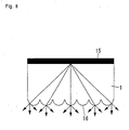
- Fig. 2(b) is a conceptual sectional view of a surface light emitting device AA which comprises the composite thin film-holding substrate A shown in Fig. 2(a), and a light-emitting element (15) in the form of a thin film, provided on the side of the composite thin film (4), which side is opposing to the substrate (1).
- light emitted by the light-emitting element (15) passes through the composite thin film (4) and the substrate (1) and goes out of the surface of the substrate (1), as indicated by the arrows.
- the composite thin film (4) is a composite layer comprising the binder (3) having a lower refractive index, and the filler (2) having a higher refractive index, and the composite thin film (4) has an average refractive index lower than the refractive index of the substrate (1).
- the light passes through the interface between the light-emitting element (15) and the composite thin film (4) and through the composite thin film (4), and further through the substrate (1). During such light passing, an incident angle of the light enters the substrate (1) from the composite thin film (4) becomes smaller, because the refractive index of the composite thin film is lower than that of the substrate (1).
- the binder (3) having the refractive index higher than that of the substrate (1) there is no particular limit in selection of the binder (3) having the refractive index higher than that of the substrate (1), in so far as the binder (3) has a refractive index higher than that of the substrate (1), and also has a light-transmitting property.
- the binder (3) the organic polymers, the metal oxides, etc. as described above are preferably used.
- the refractive index of such binder is preferably within the range of 1.5 to 1.8, and more preferably within the range of 1.5 to 1.6.
- the composite thin film (4) which has a refractive index lower than that of the substrate (1) is formed in spite of using the binder (3) having a refractive index higher than that of the substrate (1) in combination with the filler having a refractive index higher than that of the substrate (1), the fine particles of the metal oxides such as silica, titania, etc., the fine particles of the organic polymers, etc. as described above can be used as the filler (2).
- the refractive index of this filler (2) is higher than that of the substrate (1), and it is generally at least 1.46.
- the fine particles of the metal oxide are used as the filler (2)
- the refractive index of the filler (2) is preferably within the range of 1.46 to 1.6, and more preferably within the range of 1.46 to 1.55.
- the fine particles of the organic polymer are used as the filler (2)
- a smoothening backing layer is provided on a surface of the composite thin film (4) which surface is opposite to the surface on which the substrate (1) is located (that is, a surface of the film (4) opposite the substrate (1)), when the roughness of the surface of the composite thin film (4) provided on the substrate (1) is too large.
- the irregularities of the surface of the composite thin film (4) are filled with the smoothening backing layer so as to smoothen the surface of the film.
- Figs. 3(a) and 3(b) are schematic sectional views of the embodiments in which such smoothening backing layers (6) are provided on the composite thin film-holding substrates A shown in Figs.
- the smoothening backing layer (6) can be formed by the vacuum deposition process, the sputtering process, the vapor phase growth process such as CVD, the coating process in which a volatile content of an applied layer formed on the composite thin film (4) is removed by drying, or the like.
- Fig. 4 shows schematic sectional views of the embodiments in which the transparent and electrically conductive films are formed as described above, respectively.
- Each of the embodiments shown in Fig. 4 is the transparent and electrically conductive film-holding substrate B which is provided by forming a transparent and electrically conductive film (5) on the composite thin film (4) of the composite thin film-holding substrate A formed as described above.
- the smoothening backing layer (6) is provided on the surface of the composite thin film (4) opposite to the substrate (1), and the transparent and electrically conductive film (5) is formed on the smoothening backing layer (6).
- the transparent and electrically conductive film (5) may be used as an anode (or a positive electrode) in the case where an electroluminescent element is formed, as will be described later.
- indium tin oxide (ITO), zinc oxide, tin oxide, indium zinc oxide (IZO), conductive polymers or the like can be used as a material for the transparent conductive film (5), although the material is not limited to those listed above. It is also optional to appropriately select a method for forming the transparent conductive film (5) such as the vapor phase growth process, the coating process or the like, as in the case of forming the smoothening backing layer (6).
- Fig. 5 shows schematic sectional views of surface light emitting device C in which thin films (7) of a fluorescent material are provided on the composite thin films (4) of the composite thin film-holding substrates A made as described above, respectively.
- the thin film (7) of the fluorescent material is directly provided on a surface of the composite thin film (4) opposite to the surface of the film (4) on which the substrate (1) is located.
- the thin film (7) comprises an organic or inorganic fluorescent material which is excited by irradiation with UV or an electron beam to thereby emit light, and the thin film as a photoluminescent element (7) composes a surface light emitting device (C).
- Fig. 6 shows schematic sectional views of a surface light emitting devices D in each of which a light-emitting layer (8) and a metal electrode (9) are stacked (or formed) on the transparent and electrically conductive film (5) of the above described transparent and electrically conductive film-holding substrate B to form an electroluminescent element (10).
- the element (10) is formed on the composite thin film-holding substrate A.
- the electroluminescent element (10) comprises the transparent and electrically conductive film (5) as an anode, the metal electrode (9) in the form of a thin metal film as a cathode (or negative electrode), and the light-emitting layer (8) formed between the anode and the cathode.
- a solution was prepared by adding, to tetraethoxysilane (208 parts by mass), methanol (356 parts by mass), water (18 parts by mass) and 0.01N hydrochloric acid (18 parts by mass), and sufficiently mixing them with Disper.
- the resulting solution was stirred at 25°C in a constant temperature bath for 2 hours to obtain a SILICONE RESIN-M (a product obtained by hydrolyzing tetraethoxysilane and condensation-polymerizing the hydrolyzed product) as a binder-forming material having a weight-average molecular weight of 850.
- hollow silica IPA-dispersed sol solid content: 20 mass %, dispersion medium: isopropylalcohol, average primary particle diameter: about 35 nm, and shell thickness: about 8 nm, manufactured by CATALYSIS & CHEMICALS INDUSTIRES CO., LTD.
- the resulting mixture was diluted with methanol so that a whole of the solid contents was 10 mass %, and thereby a coating material composition was obtained which contained the fine and hollow silica particles.
- the wording "converted to the condensed compound” means for example that the weight of Si present in the case of tetraalkoxysilane (i.e., tetraethoxysilane in this case) is calculated to be a weight of SiO 2 , and that the weight of Si present in the case of trialkoxysilane is calculated to be a weight of SiO 1.5 .
- the coating material composition was applied to a surface of a glass plate as a substrate with a spin coater at 1,000 rpm and dried to obtain a coating film.
- the coating film was baked at 200°C for 10 minutes for the heating treatment so as to obtain a composite thin film-holding substrate having a structure as shown in Fig. 1(a). It is noted that the refractive index of the glass plate was 1.52, and that of the fine and hollow silica particles was 1.25, and that of the binder (which was obtained by applying SILICONE RESIN-M alone, and drying and thermally treating the same) was 1,45.
- methanol 64 parts by mass
- water 36 parts by mass
- 28 mass % of ammonia 0.6 parts by mass
- a 50-fold concentrated polystyrene fine particle-dispersed sol solid content: 1 mass %, and average primary particle diameter: about 100 nm, manufactured by Duke Scientific
- the coating material composition was applied to a surface of a glass plate as a substrate with a spin coater at 1,000 rpm to form a coating film. After gelation of the coating film, it was dried under supercritical conditions of 80°C and 160 kg/cm 2 to obtain a composite thin film-holding substrate having a structure as shown in Fig. 2(a). Ii is noted that the refractive index of the glass plate was 1.52; that of the fine polystyrene particles was 1.59; and that of the binder found after the supercritical drying was 1.18.
- Example 2 Only the SILICONE RESIN-M (therefore containing no fine and hollow silica particle) obtained in Example 1 was applied to a surface of a glass plate (which was the same those as those used in Examples 1 and 2) in the same manner as in Example 1, and the resulting film-holding substrate was referred to as Comparative Example 2.
- a transparent and electrically conductive thin film consisting of an ITO thin film was directly formed as Comparative Example 3 on the surface of a glass plate which was the same as those used in Examples 1 and 2, in the same manner as in Example 3.
- a transparent and electrically conductive thin film consisting of an IZO thin film was directly formed as Comparative Example 4 on the surface of a glass plate which was the same as those used in Examples 1 and 2, in the same manner as in Example 4.
- a film of aluminum tris(8-hydroquinoline) ("Alq3" manufactured by Doujindo Laboratories) with a thickness of 100 nm was formed as a thin film of a fluorescent material on the composite thin film of the composite thin film-holding substrate of Example 1.
- Alq3 aluminum tris(8-hydroquinoline)
- a surface light emitting device as shown in Fig. 5(a) was obtained as a photoluminescent element.
- a thin film of a fluorescent material was formed on the composite thin film of the composite thin film-holding substrate of Example 2 in the same manner as in Example 5.
- a surface light emitting device as shown in Fig. 5(b) was obtained as a photoluminescent element.
- a thin film of a fluorescent material was directly formed on the surface of a glass plate which was the same one as those used in Examples 1 and 2 in the same manner as in Example 5. Thus, a surface light emitting device as a photoluminescent element was obtained.
- a film of N,N-diphenyl-N,N-bis-3-methylphenyl-1,1-diphenyl-4,4-diamine ( ⁇ -NPD) with a thickness of 50 nm, a film of aluminum tris(8-hydroquinoline) (Alq3) with a thickness of 50 nm and a film of Al with a thickness of 10 nm were formed on the transparent and electrically conductive film of the transparent conductive film-holding substrate of Example 3 by the vacuum deposition process to thereby stack a hole-transporting layer, a light-emitting layer and a metal electrode.
- an organic electroluminescent element was formed, and thereby, a surface light emitting device as shown in Fig. 6(a) was obtained.
- An organic electroluminescent element was formed using the transparent and electrically conductive film-holding substrate of Example 4 in the same manner as in Example 7, and thus, a surface light emitting device as shown in Fig. 6(b) was obtained.
- An organic electroluminescent element was formed using the transparent and electrically conductive film-holding substrate of Comparative Example 3 in the same manner as in Example 7, and thus, a surface light emitting device was obtained.
- the filler which has a refractive index lower than that of the substrate and which is contained in the surface of the substrate, a quantity of such component of light that is guided within the substrate can be lessened, and thereby, the light discharge efficiency can be improved.
- a composite thin film comprising a filler having a refractive index lower than that of the substrate and a binder having a refractive index higher than that of the filler is formed, a part of light is scattered while passing through the composite thin film comprising the filler and the binder which have different refractive indexes.
- the composite thin film-holding substrate according to the third aspect of the present invention wherein the composite thin film comprising the binder having a refractive index higher than that of the substrate and the filler having a refractive index higher than that of the substrate is formed on the surface of the substrate.
- the filler having a refractive index lower than that of the substrate is selected from the fine aerogel particles, the fine and hollow silica particles, and the fine and hollow polymer particles, and wherein the binder having a refractive index higher than that of the filler is selected from the organic polymers and the metal oxides
- the effect of the composite thin film comprising a filler and a binder i.e., the effect of increasing the light discharge efficiency can be improved.
- the transparent and electrically conductive film-holding substrate of the present invention provided by forming the transparent and electrically conductive film on the composite thin film of any of the foregoing composite thin film-holding substrates can have a higher efficiency of the light discharge to its external.
- the thin film of the organic or inorganic fluorescent material which is excited by UV or an electron beam to thereby emit light is formed on the composite thin film of the composite thin film-holding substrate,and therefor, such surface light emitting device can achieve a higher efficiency of the light discharge to its external.
- the electroluminescent element is formed by stacking the light-emitting layer and a metal electrode in thus listed order on the transparent and electrically conductive film of the transparent and electrically conductive film-holding substrate, and this surface light emitting device can achieve a higher efficiency of the light discharge to its external.
Landscapes
- Physics & Mathematics (AREA)
- Chemical & Material Sciences (AREA)
- Optics & Photonics (AREA)
- General Physics & Mathematics (AREA)
- Engineering & Computer Science (AREA)
- Materials Engineering (AREA)
- Wood Science & Technology (AREA)
- Organic Chemistry (AREA)
- Life Sciences & Earth Sciences (AREA)
- Inorganic Chemistry (AREA)
- Dispersion Chemistry (AREA)
- Laminated Bodies (AREA)
- Electroluminescent Light Sources (AREA)
Priority Applications (2)
| Application Number | Priority Date | Filing Date | Title |
|---|---|---|---|
| EP10164271.8A EP2226365B1 (fr) | 2001-10-25 | 2002-10-24 | Corps émetteur pour éclairage de panneau |
| EP20110189370 EP2420539A1 (fr) | 2001-10-25 | 2002-10-24 | Substrat support de film mince composite, substrat support de film mince conducteur transparent et corps électroluminescent de surface |
Applications Claiming Priority (5)
| Application Number | Priority Date | Filing Date | Title |
|---|---|---|---|
| JP2001327879 | 2001-10-25 | ||
| JP2001327879 | 2001-10-25 | ||
| JP2001327878 | 2001-10-25 | ||
| JP2001327878 | 2001-10-25 | ||
| PCT/JP2002/011023 WO2003035389A1 (fr) | 2001-10-25 | 2002-10-24 | Substrat de support a film mince composite, substrat de support a film conducteur transparent et corps emetteur pour eclairage de panneau |
Related Child Applications (3)
| Application Number | Title | Priority Date | Filing Date |
|---|---|---|---|
| EP10164271.8A Division EP2226365B1 (fr) | 2001-10-25 | 2002-10-24 | Corps émetteur pour éclairage de panneau |
| EP10164271.8 Division-Into | 2010-05-28 | ||
| EP11189370.7 Division-Into | 2011-11-16 |
Publications (3)
| Publication Number | Publication Date |
|---|---|
| EP1445095A1 true EP1445095A1 (fr) | 2004-08-11 |
| EP1445095A4 EP1445095A4 (fr) | 2007-05-30 |
| EP1445095B1 EP1445095B1 (fr) | 2012-12-26 |
Family
ID=26624107
Family Applications (3)
| Application Number | Title | Priority Date | Filing Date |
|---|---|---|---|
| EP20020775391 Expired - Lifetime EP1445095B1 (fr) | 2001-10-25 | 2002-10-24 | Substrat de support a film mince composite, substrat de support a film conducteur transparent et corps emetteur pour eclairage de panneau |
| EP20110189370 Withdrawn EP2420539A1 (fr) | 2001-10-25 | 2002-10-24 | Substrat support de film mince composite, substrat support de film mince conducteur transparent et corps électroluminescent de surface |
| EP10164271.8A Expired - Lifetime EP2226365B1 (fr) | 2001-10-25 | 2002-10-24 | Corps émetteur pour éclairage de panneau |
Family Applications After (2)
| Application Number | Title | Priority Date | Filing Date |
|---|---|---|---|
| EP20110189370 Withdrawn EP2420539A1 (fr) | 2001-10-25 | 2002-10-24 | Substrat support de film mince composite, substrat support de film mince conducteur transparent et corps électroluminescent de surface |
| EP10164271.8A Expired - Lifetime EP2226365B1 (fr) | 2001-10-25 | 2002-10-24 | Corps émetteur pour éclairage de panneau |
Country Status (5)
| Country | Link |
|---|---|
| US (1) | US7582351B2 (fr) |
| EP (3) | EP1445095B1 (fr) |
| KR (1) | KR100671990B1 (fr) |
| TW (1) | TW574110B (fr) |
| WO (1) | WO2003035389A1 (fr) |
Cited By (27)
| Publication number | Priority date | Publication date | Assignee | Title |
|---|---|---|---|---|
| EP1766701A2 (fr) * | 2004-06-25 | 2007-03-28 | Philips Intellectual Property & Standards GmbH | Del a profil d'emittance lumineuse ameliore |
| WO2007076913A1 (fr) * | 2006-01-05 | 2007-07-12 | Merck Patent Gmbh | Diodes electroluminescentes organiques a extraction accrue de lumiere |
| EP1818693A1 (fr) * | 2006-02-14 | 2007-08-15 | DSMIP Assets B.V. | Cadre comprenant plaque de verre revêtue d'une couche anti-reflet |
| EP1840600A1 (fr) * | 2006-03-29 | 2007-10-03 | Nederlandse Organisatie voor toegepast-natuurwetenschappelijk Onderzoek TNO | Réflecteur de lumière |
| WO2008014739A2 (fr) * | 2006-07-31 | 2008-02-07 | Osram Opto Semiconductors Gmbh | Composant émetteur de rayonnement |
| WO2010031688A1 (fr) * | 2008-09-19 | 2010-03-25 | Siemens Aktiengesellschaft | Composant organique électro-optique à prélèvement et injection de lumière améliorées |
| EP1803175B1 (fr) * | 2004-10-12 | 2010-09-29 | Philips Intellectual Property & Standards GmbH | Source de lumiere electroluminescente |
| EP2251715A1 (fr) * | 2009-05-14 | 2010-11-17 | Sony Corporation | Dispositif de capture d'image à l'état solide, son procédé de fabrication et appareil électronique |
| EP2259097A3 (fr) * | 2004-11-18 | 2011-11-09 | Hitachi, Ltd. | Couche antiréflechissante, méthode de fabrication et utilisation d'une telle couche pour des élements optiques d'affichages, des supports de stockage optique et des dispositifs de conversion d'énergie solaire |
| US8088475B2 (en) | 2004-03-03 | 2012-01-03 | Hitachi, Ltd. | Anti-reflecting membrane, and display apparatus, optical storage medium and solar energy converting device having the same, and production method of the membrane |
| WO2012038592A1 (fr) * | 2010-09-23 | 2012-03-29 | Beneq Oy | Module photovoltaïque à couches minces et son procédé de production |
| WO2012054319A1 (fr) * | 2010-10-20 | 2012-04-26 | 3M Innovative Properties Company | Élément diffuseur à faible indice de réfraction comportant des vides interconnectés |
| WO2012054680A1 (fr) * | 2010-10-20 | 2012-04-26 | 3M Innovative Properties Company | Élément optique comprenant une couche poreuse à faible indice de réfraction et à couche protectrice |
| CN102460125A (zh) * | 2009-04-15 | 2012-05-16 | 3M创新有限公司 | 防止光学耦合的光学膜 |
| WO2012066871A1 (fr) * | 2010-11-17 | 2012-05-24 | Canon Kabushiki Kaisha | Film antireflet et son procédé de production |
| EP2600431A2 (fr) * | 2010-09-06 | 2013-06-05 | LG Chem, Ltd. | Substrat destiné à un dispositif électronique organique et dispositif électronique organique comprenant celui-ci |
| EP2630526A1 (fr) * | 2010-10-20 | 2013-08-28 | 3M Innovative Properties Company | Élément optiquement diffus à faible indice de réfraction |
| EP2693839A1 (fr) * | 2011-03-31 | 2014-02-05 | Asahi Glass Company, Limited | Elément de led organique, substrat transmettant la lumière et procédé de production d'un substrat transmettant la lumière |
| WO2014084012A1 (fr) * | 2012-11-30 | 2014-06-05 | シャープ株式会社 | Substrat de corps de diffusion |
| EP2830113A1 (fr) * | 2012-03-23 | 2015-01-28 | LG Chem, Ltd. | Substrat pour dispositif électronique organique |
| CN104466019A (zh) * | 2014-11-25 | 2015-03-25 | 上海交通大学 | 提高光萃取效率的结构及其方法 |
| EP2635091A4 (fr) * | 2010-10-25 | 2015-06-10 | Asahi Glass Co Ltd | Dispositif électroluminescent organique, substrat translucide et procédé pour fabriquer le dispositif électroluminescent organique |
| DE102014203382A1 (de) | 2013-12-19 | 2015-07-09 | Hilmar Kraus | Modular aufgebautes Wechselrichtersystem sowie Wandlermodule zum Aufbau eines entsprechenden Wechselrichtersystems |
| EP1640748A4 (fr) * | 2003-06-26 | 2015-11-11 | Zeon Corp | Film optique multicouche, plaque de polarisation et produit optique |
| EP3136464A1 (fr) * | 2015-08-25 | 2017-03-01 | LG Display Co., Ltd. | Dispositif d'affichage à diode électroluminescente organique et son procédé de fabrication |
| US11005075B2 (en) | 2015-09-23 | 2021-05-11 | Corning Incorporated | OLED light extraction using nanostructured coatings |
| WO2024083344A1 (fr) * | 2022-10-21 | 2024-04-25 | Huawei Technologies Co., Ltd. | Empilement d'affichage souple et appareil comprenant un tel empilement d'affichage |
Families Citing this family (68)
| Publication number | Priority date | Publication date | Assignee | Title |
|---|---|---|---|---|
| US20050109238A1 (en) * | 2001-10-25 | 2005-05-26 | Takeyuki Yamaki | Coating material composition and article having coating film formed therewith |
| TWI266073B (en) * | 2002-08-15 | 2006-11-11 | Fuji Photo Film Co Ltd | Antireflection film, polarizing plate and image display device |
| KR101237822B1 (ko) | 2003-08-28 | 2013-02-28 | 니끼 쇼꾸바이 카세이 가부시키가이샤 | 반사 방지 적층체 |
| KR101074948B1 (ko) * | 2003-12-17 | 2011-10-18 | 가부시키가이샤 브리지스톤 | 반사 방지 필름, 전자파 실드성 광 투과창재, 가스 방전형발광 패널, 플랫 디스플레이 패널, 진열창재 및 태양 전지모듈 |
| JP5005164B2 (ja) | 2004-03-03 | 2012-08-22 | 株式会社ジャパンディスプレイイースト | 発光素子,発光型表示装置及び照明装置 |
| JP4564773B2 (ja) * | 2004-04-07 | 2010-10-20 | 株式会社 日立ディスプレイズ | 発光素子及びその表示装置 |
| EP1759428B1 (fr) * | 2004-06-14 | 2016-05-18 | Philips Intellectual Property & Standards GmbH | Del presentant un profil d'emission de lumiere ameliore |
| WO2006014002A1 (fr) * | 2004-08-03 | 2006-02-09 | Fujifilm Corporation | Film antireflet, méthode de production, plaque polarisante, affichage à cristaux liquides |
| US20080088925A1 (en) * | 2004-08-12 | 2008-04-17 | Fujifilm Corporation | Antireflection Film, Polarizing Plate And Image Display Utilizing The Same |
| CN101052685B (zh) * | 2004-09-22 | 2011-05-04 | 富士胶片株式会社 | 固化组合物、抗反射薄膜及其生产方法、偏振片以及图像显示装置 |
| US20060097385A1 (en) | 2004-10-25 | 2006-05-11 | Negley Gerald H | Solid metal block semiconductor light emitting device mounting substrates and packages including cavities and heat sinks, and methods of packaging same |
| US20060124953A1 (en) * | 2004-12-14 | 2006-06-15 | Negley Gerald H | Semiconductor light emitting device mounting substrates and packages including cavities and cover plates, and methods of packaging same |
| US7322732B2 (en) | 2004-12-23 | 2008-01-29 | Cree, Inc. | Light emitting diode arrays for direct backlighting of liquid crystal displays |
| US7304694B2 (en) | 2005-01-12 | 2007-12-04 | Cree, Inc. | Solid colloidal dispersions for backlighting of liquid crystal displays |
| JP2006308844A (ja) * | 2005-04-28 | 2006-11-09 | Seiko Epson Corp | プラスチックレンズ及びプラスチックレンズの製造方法 |
| EP1784465B1 (fr) * | 2005-06-02 | 2014-01-08 | LG Chem, Ltd. | Composition de revetement pour film a faible indice de refraction et film prepare a partir de cette composition |
| TW200739466A (en) * | 2005-11-16 | 2007-10-16 | Pentax Corp | Protective cover for display panel and its use |
| JP4678775B2 (ja) * | 2005-12-14 | 2011-04-27 | 株式会社 日立ディスプレイズ | 冷陰極蛍光管及びこの冷陰極蛍光管を用いた液晶表示装置 |
| WO2007139781A2 (fr) | 2006-05-23 | 2007-12-06 | Cree Led Lighting Solutions, Inc. | Dispositif d'éclairage |
| JP4984824B2 (ja) * | 2006-10-26 | 2012-07-25 | 豊田合成株式会社 | 発光装置 |
| US20080138538A1 (en) * | 2006-12-06 | 2008-06-12 | General Electric Company | Barrier layer, composite article comprising the same, electroactive device, and method |
| EP2125941B1 (fr) * | 2007-02-26 | 2013-05-01 | Saint-Gobain Performance Plastics Chaineux S.A. | Structure stratifiée comprenant des nanoparticules |
| JP5536977B2 (ja) * | 2007-03-30 | 2014-07-02 | パナソニック株式会社 | 面発光体 |
| KR100893617B1 (ko) * | 2007-05-23 | 2009-04-20 | 삼성에스디아이 주식회사 | 플라즈마 디스플레이 패널 및 필터 |
| US7982396B2 (en) * | 2007-06-04 | 2011-07-19 | Global Oled Technology Llc | Light-emitting device with light-scattering particles and method of making the same |
| CN101408628A (zh) * | 2007-10-10 | 2009-04-15 | 群康科技(深圳)有限公司 | 扩散片及其制造工艺、背光模组及液晶显示装置 |
| US8158247B2 (en) * | 2008-01-30 | 2012-04-17 | Los Alamos National Security, Llc | Porous light-emitting compositions |
| JP4867938B2 (ja) * | 2008-03-18 | 2012-02-01 | コニカミノルタビジネステクノロジーズ株式会社 | 表示部材 |
| US8153249B2 (en) * | 2008-08-26 | 2012-04-10 | Snu R&Db Foundation | Article treated with silica particles and method for treating a surface of the article |
| KR101148886B1 (ko) * | 2009-05-13 | 2012-05-29 | 네오뷰코오롱 주식회사 | 유기전계발광소자 및 그 제조방법 |
| EP2557896B1 (fr) * | 2010-04-08 | 2019-10-30 | AGC Inc. | Elément à diodes électroluminescentes organiques, substrat translucide et procédé de fabrication d'un élément à diodes électroluminescentes organiques |
| US9214639B2 (en) * | 2010-06-24 | 2015-12-15 | Massachusetts Institute Of Technology | Conductive polymer on a textured or plastic substrate |
| US8469551B2 (en) * | 2010-10-20 | 2013-06-25 | 3M Innovative Properties Company | Light extraction films for increasing pixelated OLED output with reduced blur |
| CN102588816B (zh) * | 2011-01-07 | 2017-12-01 | 晶元光电股份有限公司 | 发光装置、混光装置及发光装置的制造方法 |
| CN102588752A (zh) * | 2011-01-07 | 2012-07-18 | 晶元光电股份有限公司 | 发光装置 |
| JP5679565B2 (ja) | 2011-03-10 | 2015-03-04 | パナソニックIpマネジメント株式会社 | 透明導電膜、透明導電膜付き基材、及びそれを用いた有機エレクトロルミネッセンス素子 |
| EP2734871B1 (fr) * | 2011-07-21 | 2022-09-07 | Canon Kabushiki Kaisha | Élément optique et son procédé de production |
| JP6053262B2 (ja) * | 2011-08-02 | 2016-12-27 | キヤノン株式会社 | 光学素子、それを用いた光学系および光学機器 |
| TWI422628B (zh) * | 2011-09-02 | 2014-01-11 | Univ Nat Taiwan | 奈米金屬-聚合物複合導電薄膜與其製備方法 |
| US9054338B2 (en) * | 2011-09-30 | 2015-06-09 | General Electric Company | OLED devices comprising hollow objects |
| JP2013140244A (ja) * | 2011-12-30 | 2013-07-18 | Toyota Tsusho Corp | 光透過性組成物 |
| DE102012200084B4 (de) | 2012-01-04 | 2021-05-12 | Pictiva Displays International Limited | Strahlungsemittierendes organisches bauteil |
| KR101335642B1 (ko) * | 2012-02-13 | 2013-12-03 | 한국기계연구원 | 유기 발광 표시 장치 및 그 제조 방법 |
| KR101404159B1 (ko) * | 2012-02-14 | 2014-06-11 | 한국기계연구원 | 유기 발광 표시 장치의 제조 방법 |
| US9360747B2 (en) * | 2012-03-02 | 2016-06-07 | Mitsubishi Paper Mills Limited | Transmission type screen |
| KR101589344B1 (ko) * | 2012-03-30 | 2016-01-28 | 주식회사 엘지화학 | 유기전자소자용 기판 |
| WO2013152256A1 (fr) * | 2012-04-05 | 2013-10-10 | Corning Incorporated | Procédés et appareil pour la fourniture de composants d'affichage |
| JP2014077117A (ja) * | 2012-09-21 | 2014-05-01 | Dow Corning Toray Co Ltd | 高屈折性表面処理剤、それを用いて表面処理された微細部材および光学材料 |
| TWI595682B (zh) * | 2013-02-08 | 2017-08-11 | 晶元光電股份有限公司 | 發光元件 |
| JP6071661B2 (ja) * | 2013-03-11 | 2017-02-01 | 株式会社東芝 | 半導体発光装置 |
| KR20140132589A (ko) * | 2013-05-08 | 2014-11-18 | 코닝정밀소재 주식회사 | 유기발광소자용 광추출 기판, 그 제조방법 및 이를 포함하는 유기발광소자 |
| JP2015011163A (ja) * | 2013-06-28 | 2015-01-19 | キヤノン株式会社 | 光学部材及び撮像装置 |
| TWI540222B (zh) * | 2014-12-05 | 2016-07-01 | 國立清華大學 | 金屬化基板表面的方法及具有金屬化表面的基板 |
| JP6604781B2 (ja) | 2014-12-26 | 2019-11-13 | 日東電工株式会社 | 積層フィルムロールおよびその製造方法 |
| JP6599699B2 (ja) | 2014-12-26 | 2019-10-30 | 日東電工株式会社 | 触媒作用を介して結合した空隙構造フィルムおよびその製造方法 |
| JP6713872B2 (ja) | 2015-07-31 | 2020-06-24 | 日東電工株式会社 | 積層フィルム、積層フィルムの製造方法、光学部材、画像表示装置、光学部材の製造方法および画像表示装置の製造方法 |
| JP6713871B2 (ja) | 2015-07-31 | 2020-06-24 | 日東電工株式会社 | 光学積層体、光学積層体の製造方法、光学部材、画像表示装置、光学部材の製造方法および画像表示装置の製造方法 |
| JP6892744B2 (ja) | 2015-08-24 | 2021-06-23 | 日東電工株式会社 | 積層光学フィルム、積層光学フィルムの製造方法、光学部材、および画像表示装置 |
| JP7152130B2 (ja) * | 2015-09-07 | 2022-10-12 | 日東電工株式会社 | 低屈折率層、積層フィルム、低屈折率層の製造方法、積層フィルムの製造方法、光学部材および画像表示装置 |
| EP3199984A1 (fr) * | 2016-02-01 | 2017-08-02 | Canon Kabushiki Kaisha | Film antireflet, élément optique et procédé de fabrication d'élément optique |
| US10995184B2 (en) * | 2016-03-25 | 2021-05-04 | Show A Denko Materials Co., Ltd. | Sol composition, aerogel composite, support member provided with aerogel composite, and heat insulator |
| CN105891936B (zh) * | 2016-05-20 | 2019-11-01 | 京东方科技集团股份有限公司 | 导光元件及其制作方法以及背光模组 |
| WO2018062856A1 (fr) | 2016-09-27 | 2018-04-05 | 주식회사 엘지화학 | Film antiréflexion |
| US10700242B2 (en) * | 2016-12-27 | 2020-06-30 | Nichia Corporation | Method of producing wavelength conversion member |
| CN107402416B (zh) * | 2017-08-31 | 2020-10-30 | 深圳市华星光电技术有限公司 | 量子扩散膜及其制作方法 |
| CN109638175A (zh) * | 2018-11-30 | 2019-04-16 | 武汉华星光电半导体显示技术有限公司 | 有机发光装置及阵列基板 |
| KR102510532B1 (ko) * | 2019-06-10 | 2023-03-14 | 삼성에스디아이 주식회사 | 색 변환 패널 |
| CN113703226B (zh) * | 2021-09-08 | 2022-09-27 | 广东粤港澳大湾区国家纳米科技创新研究院 | 高亮度、防蓝光量子点光学板及其制备方法和背光模组 |
Citations (1)
| Publication number | Priority date | Publication date | Assignee | Title |
|---|---|---|---|---|
| DE4418214A1 (de) * | 1994-05-25 | 1995-11-30 | Gerd Hugo | Anstrichstoff mit niedrigem Emissionsvermögen im Bereich der Wärmestrahlung |
Family Cites Families (52)
| Publication number | Priority date | Publication date | Assignee | Title |
|---|---|---|---|---|
| US3966668A (en) | 1974-03-01 | 1976-06-29 | The Firestone Tire & Rubber Company | Carbon black dispersions and method of making same |
| US3969559A (en) | 1975-05-27 | 1976-07-13 | Monsanto Company | Man-made textile antistatic strand |
| US4402827A (en) | 1980-07-11 | 1983-09-06 | Sealed Power Corporation | Transmission fluid filter |
| FR2507171A1 (fr) | 1981-06-04 | 1982-12-10 | Zarzycki Jerzy | Aerogels de silice monolithiques, leur preparation et leur utilisation pour la preparation d'articles en verre de silice et de materiaux thermiquement isolants |
| JPS60213901A (ja) | 1984-04-09 | 1985-10-26 | Seiko Epson Corp | 合成樹脂製レンズ |
| US4610863A (en) | 1985-09-04 | 1986-09-09 | The United States Of America As Represented By The United States Department Of Energy | Process for forming transparent aerogel insulating arrays |
| US5742118A (en) * | 1988-09-09 | 1998-04-21 | Hitachi, Ltd. | Ultrafine particle film, process for producing the same, transparent plate and image display plate |
| DE4038784A1 (de) | 1990-12-05 | 1992-06-11 | Basf Ag | Verbundschaumstoffe mit niedriger waermeleitfaehigkeit |
| US5137279A (en) | 1991-02-13 | 1992-08-11 | Campaign Headquarters, Inc. | Political candidate campaign board game |
| US5665422A (en) * | 1991-03-19 | 1997-09-09 | Hitachi, Ltd. | Process for formation of an ultra fine particle film |
| JP2659155B2 (ja) | 1992-02-03 | 1997-09-30 | 松下電工株式会社 | 疎水性エアロゲルの製造方法 |
| JPH063501A (ja) | 1992-06-23 | 1994-01-14 | Dainippon Printing Co Ltd | 多孔質光学材料 |
| JPH0748527A (ja) | 1993-08-06 | 1995-02-21 | Sumitomo Osaka Cement Co Ltd | 反射防止層を有する光学材料及びその製造方法 |
| JP2725573B2 (ja) | 1993-11-12 | 1998-03-11 | 松下電工株式会社 | 疎水性エアロゲルの製法 |
| JPH07247144A (ja) | 1994-03-09 | 1995-09-26 | Aica Kogyo Co Ltd | 導電性軽量骨材及びその製法 |
| US20010044489A1 (en) | 1994-05-25 | 2001-11-22 | Gerd Hugo | Coating substance with low emissivity in the heat radiation range |
| JPH0811631A (ja) | 1994-06-29 | 1996-01-16 | Murakami Kaimeidou:Kk | 車両用ミラー |
| US5607764A (en) | 1994-10-27 | 1997-03-04 | Fuji Photo Film Co., Ltd. | Optical diffuser |
| EP0816466B1 (fr) | 1995-03-20 | 2006-05-17 | Toto Ltd. | Utilisation d'un materiau ayant une surface ultrahydrophile et photocatalytique |
| US6090873A (en) | 1995-04-21 | 2000-07-18 | Matsushita Electric Works, Ltd. | Coating resin composition containing a hydrolyzable organosilane and an acrylic resin |
| JP3351666B2 (ja) | 1995-10-20 | 2002-12-03 | 株式会社中戸研究所 | 防曇性反射防止膜、光学部品、及び防曇性反射防止膜の製造方法 |
| JPH09115334A (ja) | 1995-10-23 | 1997-05-02 | Mitsubishi Materiais Corp | 透明導電膜および膜形成用組成物 |
| EP0778476A3 (fr) | 1995-12-07 | 1998-09-09 | Fuji Photo Film Co., Ltd. | Couche antiréfléchissante et dispositif d'affichage avec cette couche |
| US6040053A (en) | 1996-07-19 | 2000-03-21 | Minnesota Mining And Manufacturing Company | Coating composition having anti-reflective and anti-fogging properties |
| JP2901550B2 (ja) | 1996-07-26 | 1999-06-07 | 株式会社村上開明堂 | 防曇素子 |
| JP3431415B2 (ja) | 1996-09-20 | 2003-07-28 | 恵和株式会社 | 光拡散シート |
| JPH10142402A (ja) | 1996-11-06 | 1998-05-29 | Fuji Photo Film Co Ltd | 反射防止膜およびそれを配置した表示装置 |
| US6210858B1 (en) | 1997-04-04 | 2001-04-03 | Fuji Photo Film Co., Ltd. | Anti-reflection film and display device using the same |
| JP3967822B2 (ja) | 1997-04-04 | 2007-08-29 | 富士フイルム株式会社 | 反射防止膜およびそれを用いた画像表示装置 |
| FR2765884B1 (fr) | 1997-07-09 | 2001-07-27 | Rhodia Chimie Sa | Composition silicone pour l'enduction de substrats en matiere souple, notamment textile |
| JP4642165B2 (ja) | 1997-08-07 | 2011-03-02 | 日揮触媒化成株式会社 | 多孔質シリカ系被膜形成用塗布液、被膜付基材および短繊維状シリカ |
| JP4101339B2 (ja) | 1997-09-25 | 2008-06-18 | 大日本印刷株式会社 | 光拡散フィルム、その製造方法、拡散層付偏光板及び液晶表示装置 |
| JPH11315223A (ja) | 1997-12-16 | 1999-11-16 | Leben Utility Kk | 建材用塗料組成物、並びにこれを用いた塗膜及び建材 |
| ATE403707T1 (de) | 1998-04-10 | 2008-08-15 | Matsushita Electric Works Ltd | Verfahren zur herstellung eines hydrophilen anorganischen beschichtungsfilms und eine zusammensetzung für anorganische beschichtungen |
| JP3862413B2 (ja) | 1998-05-12 | 2006-12-27 | 富士フイルムホールディングス株式会社 | 反射防止膜およびそれを用いた画像表示装置 |
| JPH11329742A (ja) | 1998-05-18 | 1999-11-30 | Idemitsu Kosan Co Ltd | 有機エレクトロルミネッセンス素子および発光装置 |
| KR100347666B1 (ko) | 1998-09-08 | 2002-11-18 | 주식회사 엘지화학 | 투명한 대전방지 내마모성 피복 조성물 및 그의 제조방법 |
| JP3384983B2 (ja) | 1999-08-27 | 2003-03-10 | 恵和株式会社 | 光拡散シート及びこれを用いたバックライトユニット |
| ATE391303T1 (de) | 1999-09-28 | 2008-04-15 | Fujifilm Corp | Antireflexbeschichtung, damit versehene polarisationsplatte, und bildanzeigegerät mit der antireflexbeschichtung oder mit der polarisationsplatte |
| JP4836316B2 (ja) | 1999-09-29 | 2011-12-14 | 富士フイルム株式会社 | 反射防止膜、偏光板、及び画像表示装置 |
| EP1100129B1 (fr) | 1999-11-10 | 2006-03-22 | Matsushita Electric Works, Ltd. | Substrat pour dispositif émetteur de lumière, dispositif émetteur de lumière et méthode de fabrication |
| JP4279971B2 (ja) | 1999-11-10 | 2009-06-17 | パナソニック電工株式会社 | 発光素子 |
| US6762553B1 (en) | 1999-11-10 | 2004-07-13 | Matsushita Electric Works, Ltd. | Substrate for light emitting device, light emitting device and process for production of light emitting device |
| JP2001154004A (ja) | 1999-11-24 | 2001-06-08 | Keiwa Inc | 光学シート及びこれを用いたバックライトユニット |
| JP4046921B2 (ja) | 2000-02-24 | 2008-02-13 | 触媒化成工業株式会社 | シリカ系微粒子、該微粒子分散液の製造方法、および被膜付基材 |
| JP4031624B2 (ja) | 2000-06-23 | 2008-01-09 | 株式会社東芝 | 透明被膜付基材、透明被膜形成用塗布液、および表示装置 |
| JP4918743B2 (ja) | 2001-02-16 | 2012-04-18 | 凸版印刷株式会社 | 反射防止フィルム |
| US20050109238A1 (en) * | 2001-10-25 | 2005-05-26 | Takeyuki Yamaki | Coating material composition and article having coating film formed therewith |
| JP3899011B2 (ja) | 2001-10-25 | 2007-03-28 | 松下電工株式会社 | 面発光体 |
| JP2003202406A (ja) | 2001-10-25 | 2003-07-18 | Matsushita Electric Works Ltd | 反射防止フィルム及びディスプレイ装置 |
| JP2003149642A (ja) | 2001-11-13 | 2003-05-21 | Matsushita Electric Works Ltd | 液晶用フロントライト |
| JP2003161816A (ja) * | 2001-11-29 | 2003-06-06 | Nitto Denko Corp | 光拡散性シート、光学素子および表示装置 |
-
2002
- 2002-10-24 EP EP20020775391 patent/EP1445095B1/fr not_active Expired - Lifetime
- 2002-10-24 EP EP20110189370 patent/EP2420539A1/fr not_active Withdrawn
- 2002-10-24 TW TW91124796A patent/TW574110B/zh not_active IP Right Cessation
- 2002-10-24 WO PCT/JP2002/011023 patent/WO2003035389A1/fr active Application Filing
- 2002-10-24 KR KR1020047005965A patent/KR100671990B1/ko active IP Right Grant
- 2002-10-24 US US10/492,534 patent/US7582351B2/en active Active
- 2002-10-24 EP EP10164271.8A patent/EP2226365B1/fr not_active Expired - Lifetime
Patent Citations (1)
| Publication number | Priority date | Publication date | Assignee | Title |
|---|---|---|---|---|
| DE4418214A1 (de) * | 1994-05-25 | 1995-11-30 | Gerd Hugo | Anstrichstoff mit niedrigem Emissionsvermögen im Bereich der Wärmestrahlung |
Non-Patent Citations (1)
| Title |
|---|
| See also references of WO03035389A1 * |
Cited By (62)
| Publication number | Priority date | Publication date | Assignee | Title |
|---|---|---|---|---|
| EP1640748A4 (fr) * | 2003-06-26 | 2015-11-11 | Zeon Corp | Film optique multicouche, plaque de polarisation et produit optique |
| US8088475B2 (en) | 2004-03-03 | 2012-01-03 | Hitachi, Ltd. | Anti-reflecting membrane, and display apparatus, optical storage medium and solar energy converting device having the same, and production method of the membrane |
| EP1766701A2 (fr) * | 2004-06-25 | 2007-03-28 | Philips Intellectual Property & Standards GmbH | Del a profil d'emittance lumineuse ameliore |
| EP1803175B1 (fr) * | 2004-10-12 | 2010-09-29 | Philips Intellectual Property & Standards GmbH | Source de lumiere electroluminescente |
| EP2259097A3 (fr) * | 2004-11-18 | 2011-11-09 | Hitachi, Ltd. | Couche antiréflechissante, méthode de fabrication et utilisation d'une telle couche pour des élements optiques d'affichages, des supports de stockage optique et des dispositifs de conversion d'énergie solaire |
| WO2007076913A1 (fr) * | 2006-01-05 | 2007-07-12 | Merck Patent Gmbh | Diodes electroluminescentes organiques a extraction accrue de lumiere |
| US8125145B2 (en) | 2006-01-05 | 2012-02-28 | Merck Patent Gmbh | OLEDs with increased light yield |
| EP1818693A1 (fr) * | 2006-02-14 | 2007-08-15 | DSMIP Assets B.V. | Cadre comprenant plaque de verre revêtue d'une couche anti-reflet |
| WO2007093341A1 (fr) * | 2006-02-14 | 2007-08-23 | Dsm Ip Assets B.V. | Revetements antireflecteurs |
| EP1840600A1 (fr) * | 2006-03-29 | 2007-10-03 | Nederlandse Organisatie voor toegepast-natuurwetenschappelijk Onderzoek TNO | Réflecteur de lumière |
| WO2007111511A1 (fr) * | 2006-03-29 | 2007-10-04 | Nederlandse Organisatie Voor Toegepast-Natuurwetenschappelijk Onderzoek Tno | réflecteur de lumière |
| WO2008014739A2 (fr) * | 2006-07-31 | 2008-02-07 | Osram Opto Semiconductors Gmbh | Composant émetteur de rayonnement |
| WO2008014739A3 (fr) * | 2006-07-31 | 2008-05-08 | Osram Opto Semiconductors Gmbh | Composant émetteur de rayonnement |
| WO2010031688A1 (fr) * | 2008-09-19 | 2010-03-25 | Siemens Aktiengesellschaft | Composant organique électro-optique à prélèvement et injection de lumière améliorées |
| CN102460125B (zh) * | 2009-04-15 | 2015-11-25 | 3M创新有限公司 | 防止光学耦合的光学膜 |
| CN102460125A (zh) * | 2009-04-15 | 2012-05-16 | 3M创新有限公司 | 防止光学耦合的光学膜 |
| US8355072B2 (en) | 2009-05-14 | 2013-01-15 | Sony Corporation | Solid-state image capture device, manufacturing method therefor, and electronic apparatus |
| EP2251715A1 (fr) * | 2009-05-14 | 2010-11-17 | Sony Corporation | Dispositif de capture d'image à l'état solide, son procédé de fabrication et appareil électronique |
| EP2662710A1 (fr) * | 2009-05-14 | 2013-11-13 | Sony Corporation | Dispositif de capture d'image à l'état solide et son procédé de fabrication |
| US8902348B2 (en) | 2009-05-14 | 2014-12-02 | Sony Corporation | Solid-state image capture device, manufacturing method therefor, and electronic apparatus |
| CN103201869B (zh) * | 2010-09-06 | 2016-06-15 | 乐金显示有限公司 | 有机电子器件用衬底和包括该衬底的有机电子器件 |
| US9257675B2 (en) | 2010-09-06 | 2016-02-09 | Lg Chem, Ltd. | Substrate for an organic electronic device and an organic electronic device comprising the same |
| EP2600431A2 (fr) * | 2010-09-06 | 2013-06-05 | LG Chem, Ltd. | Substrat destiné à un dispositif électronique organique et dispositif électronique organique comprenant celui-ci |
| CN103201869A (zh) * | 2010-09-06 | 2013-07-10 | 株式会社Lg化学 | 有机电子器件用衬底和包括该衬底的有机电子器件 |
| EP2600431A4 (fr) * | 2010-09-06 | 2014-07-02 | Lg Chemical Ltd | Substrat destiné à un dispositif électronique organique et dispositif électronique organique comprenant celui-ci |
| WO2012038592A1 (fr) * | 2010-09-23 | 2012-03-29 | Beneq Oy | Module photovoltaïque à couches minces et son procédé de production |
| WO2012054319A1 (fr) * | 2010-10-20 | 2012-04-26 | 3M Innovative Properties Company | Élément diffuseur à faible indice de réfraction comportant des vides interconnectés |
| EP2630524B1 (fr) * | 2010-10-20 | 2021-02-17 | 3M Innovative Properties Company | Élélement optique avec une couche poreuse à bas indice et une couche protectrice |
| US10502869B2 (en) | 2010-10-20 | 2019-12-10 | 3M Innovative Properties Company | Optical element with a porous low refractive index layer having a protection layer |
| EP2630525B1 (fr) * | 2010-10-20 | 2018-09-05 | 3M Innovative Properties Company | Élément diffuseur à bas indice avec cannaux interconnectés |
| EP2630526A1 (fr) * | 2010-10-20 | 2013-08-28 | 3M Innovative Properties Company | Élément optiquement diffus à faible indice de réfraction |
| CN103168257B (zh) * | 2010-10-20 | 2017-03-01 | 3M创新有限公司 | 具有多孔低折射率层并且具有保护层的光学元件 |
| US9465145B2 (en) | 2010-10-20 | 2016-10-11 | 3M Innovative Properties Company | Low refractive index diffuser element having interconnected voids |
| WO2012054680A1 (fr) * | 2010-10-20 | 2012-04-26 | 3M Innovative Properties Company | Élément optique comprenant une couche poreuse à faible indice de réfraction et à couche protectrice |
| CN103168257A (zh) * | 2010-10-20 | 2013-06-19 | 3M创新有限公司 | 具有多孔低折射率层并且具有保护层的光学元件 |
| EP2635091A4 (fr) * | 2010-10-25 | 2015-06-10 | Asahi Glass Co Ltd | Dispositif électroluminescent organique, substrat translucide et procédé pour fabriquer le dispositif électroluminescent organique |
| WO2012066871A1 (fr) * | 2010-11-17 | 2012-05-24 | Canon Kabushiki Kaisha | Film antireflet et son procédé de production |
| CN103210045A (zh) * | 2010-11-17 | 2013-07-17 | 佳能株式会社 | 减反射膜及其制备方法 |
| CN103210045B (zh) * | 2010-11-17 | 2015-05-20 | 佳能株式会社 | 减反射膜及其制备方法 |
| US20130222916A1 (en) * | 2010-11-17 | 2013-08-29 | Canon Kabushiki Kaisha | Antireflection film and method of producing the same |
| US9798045B2 (en) | 2010-11-17 | 2017-10-24 | Canon Kabushiki Kaisha | Antireflection film and method of producing the same |
| EP2693839A1 (fr) * | 2011-03-31 | 2014-02-05 | Asahi Glass Company, Limited | Elément de led organique, substrat transmettant la lumière et procédé de production d'un substrat transmettant la lumière |
| EP2693839A4 (fr) * | 2011-03-31 | 2014-11-26 | Asahi Glass Co Ltd | Elément de led organique, substrat transmettant la lumière et procédé de production d'un substrat transmettant la lumière |
| EP2830114B1 (fr) * | 2012-03-23 | 2018-12-19 | LG Display Co., Ltd. | Substrat pour dispositif électronique organique |
| US9716242B2 (en) | 2012-03-23 | 2017-07-25 | Lg Display Co., Ltd. | Substrate for organic electronic device |
| EP2830114A1 (fr) * | 2012-03-23 | 2015-01-28 | LG Chem, Ltd. | Substrat pour dispositif électronique organique |
| US9530979B2 (en) | 2012-03-23 | 2016-12-27 | Lg Display Co., Ltd. | Substrate for organic electronic device |
| EP2830111A4 (fr) * | 2012-03-23 | 2015-12-30 | Lg Chemical Ltd | Substrat pour dispositif électronique organique |
| EP2830113A1 (fr) * | 2012-03-23 | 2015-01-28 | LG Chem, Ltd. | Substrat pour dispositif électronique organique |
| EP2830116A4 (fr) * | 2012-03-23 | 2015-12-30 | Lg Chemical Ltd | Substrat pour dispositif électronique organique |
| US9666828B2 (en) | 2012-03-23 | 2017-05-30 | Lg Display Co., Ltd. | Method for producing a substrate for organic electronic devices |
| US9698366B2 (en) | 2012-03-23 | 2017-07-04 | Lg Display Co., Ltd. | Substrate for organic electronic device |
| EP2830113A4 (fr) * | 2012-03-23 | 2015-12-30 | Lg Chemical Ltd | Substrat pour dispositif électronique organique |
| WO2014084012A1 (fr) * | 2012-11-30 | 2014-06-05 | シャープ株式会社 | Substrat de corps de diffusion |
| DE102014203382A1 (de) | 2013-12-19 | 2015-07-09 | Hilmar Kraus | Modular aufgebautes Wechselrichtersystem sowie Wandlermodule zum Aufbau eines entsprechenden Wechselrichtersystems |
| CN104466019A (zh) * | 2014-11-25 | 2015-03-25 | 上海交通大学 | 提高光萃取效率的结构及其方法 |
| CN106486519A (zh) * | 2015-08-25 | 2017-03-08 | 乐金显示有限公司 | 有机发光二极管显示装置及用于有机发光二极管显示装置的聚合物纳米颗粒 |
| US10243169B2 (en) | 2015-08-25 | 2019-03-26 | Lg Display Co., Ltd. | Organic light emitting diode display device including nanoparticles and method of fabricating the same |
| CN106486519B (zh) * | 2015-08-25 | 2019-08-09 | 乐金显示有限公司 | 有机发光二极管显示装置及用于有机发光二极管显示装置的聚合物纳米颗粒 |
| EP3136464A1 (fr) * | 2015-08-25 | 2017-03-01 | LG Display Co., Ltd. | Dispositif d'affichage à diode électroluminescente organique et son procédé de fabrication |
| US11005075B2 (en) | 2015-09-23 | 2021-05-11 | Corning Incorporated | OLED light extraction using nanostructured coatings |
| WO2024083344A1 (fr) * | 2022-10-21 | 2024-04-25 | Huawei Technologies Co., Ltd. | Empilement d'affichage souple et appareil comprenant un tel empilement d'affichage |
Also Published As
| Publication number | Publication date |
|---|---|
| KR100671990B1 (ko) | 2007-01-24 |
| WO2003035389A1 (fr) | 2003-05-01 |
| EP1445095B1 (fr) | 2012-12-26 |
| US7582351B2 (en) | 2009-09-01 |
| EP2420539A1 (fr) | 2012-02-22 |
| US20040253427A1 (en) | 2004-12-16 |
| TW574110B (en) | 2004-02-01 |
| EP2226365A1 (fr) | 2010-09-08 |
| EP2226365B1 (fr) | 2016-08-10 |
| KR20040047949A (ko) | 2004-06-05 |
| EP1445095A4 (fr) | 2007-05-30 |
Similar Documents
| Publication | Publication Date | Title |
|---|---|---|
| US7582351B2 (en) | Composite thin film holding substrate, transparent conductive film holding substrate, and panel light emitting body | |
| JP3899011B2 (ja) | 面発光体 | |
| KR100385413B1 (ko) | 발광소자용 기판, 발광소자 및 발광소자의 제조방법 | |
| JP4279971B2 (ja) | 発光素子 | |
| US20090026924A1 (en) | Methods of making low-refractive index and/or low-k organosilicate coatings | |
| US20080157665A1 (en) | Optical Thin Films with Nano-Corrugated Surface Topologies by a Simple Coating Method | |
| CN101790899A (zh) | 有机el发光元件 | |
| EP1100129A2 (fr) | Substrat pour dispositif émetteur de lumière, dispositif émetteur de lumière et méthode de fabrication | |
| US9263701B2 (en) | Coated article and/or device with optical out-coupling layer stack (OCLS) including vacuum deposited index match layer over scattering matrix, and/or associated methods | |
| TW201220549A (en) | Light source, device including light source, and/or methods of making the same | |
| JP2007134339A (ja) | 面発光体 | |
| TW201224081A (en) | Light source with hybrid coating, device including light source with hybrid coating, and/or methods of making the same | |
| US8917014B2 (en) | Coated articles and/or devices with optical out-coupling layer stacks (OCLS), and/or methods of making the same | |
| WO2009007919A2 (fr) | Diodes électroluminescentes organiques ayant un meilleur découplage optique | |
| JP2003119052A (ja) | 光透過シート、これを用いた発光装置、及び、光透過シートの製造方法 | |
| KR101735445B1 (ko) | 고굴절 및 저굴절 유/무기 하이브리드 재료를 이용한 oled 소자용 적층체 및 oled 소자의 제조방법, 이에 의해 제조되는 oled 소자 | |
| JP2007294266A (ja) | 有機el素子 | |
| JP2021182134A (ja) | 防曇性多孔質酸化ケイ素膜およびその製造方法 | |
| JP2020063180A (ja) | 表面被覆層形成用塗工液及び多孔質ケイ素積層体 | |
| US12122879B2 (en) | Curable resin composition, thin film, and color conversion panel and display device including thin film | |
| JP2010079053A (ja) | 低屈折率膜、反射防止膜、透明部材、蛍光ランプ | |
| JP2015099333A (ja) | 反射防止膜 | |
| JP2010080320A (ja) | 酸化物微粒子含有塗料、透過率向上膜、蛍光ランプ、表示機器 | |
| JP2007180037A (ja) | 発光素子、平面発光板、平面発光板の製造方法、平面蛍光ランプ、プラズマディスプレイ |
Legal Events
| Date | Code | Title | Description |
|---|---|---|---|
| PUAI | Public reference made under article 153(3) epc to a published international application that has entered the european phase |
Free format text: ORIGINAL CODE: 0009012 |
|
| 17P | Request for examination filed |
Effective date: 20040428 |
|
| AK | Designated contracting states |
Kind code of ref document: A1 Designated state(s): AT BE BG CH CY CZ DE DK EE ES FI FR GB GR IE IT LI LU MC NL PT SE SK TR |
|
| AX | Request for extension of the european patent |
Extension state: AL LT LV MK RO SI |
|
| A4 | Supplementary search report drawn up and despatched |
Effective date: 20070427 |
|
| RIC1 | Information provided on ipc code assigned before grant |
Ipc: H05B 33/14 20060101ALI20030508BHEP Ipc: G02B 5/02 20060101ALI20030508BHEP Ipc: C09D 7/12 20060101AFI20070423BHEP Ipc: G02F 1/133 20060101ALI20030508BHEP Ipc: H05B 33/02 20060101ALI20030508BHEP |
|
| RAP1 | Party data changed (applicant data changed or rights of an application transferred) |
Owner name: PANASONIC ELECTRIC WORKS CO., LTD. |
|
| 17Q | First examination report despatched |
Effective date: 20091119 |
|
| RAP1 | Party data changed (applicant data changed or rights of an application transferred) |
Owner name: PANASONIC CORPORATION |
|
| GRAP | Despatch of communication of intention to grant a patent |
Free format text: ORIGINAL CODE: EPIDOSNIGR1 |
|
| GRAS | Grant fee paid |
Free format text: ORIGINAL CODE: EPIDOSNIGR3 |
|
| GRAA | (expected) grant |
Free format text: ORIGINAL CODE: 0009210 |
|
| AK | Designated contracting states |
Kind code of ref document: B1 Designated state(s): DE FR GB NL |
|
| REG | Reference to a national code |
Ref country code: GB Ref legal event code: FG4D |
|
| REG | Reference to a national code |
Ref country code: DE Ref legal event code: R096 Ref document number: 60244298 Country of ref document: DE Effective date: 20130307 |
|
| REG | Reference to a national code |
Ref country code: NL Ref legal event code: VDEP Effective date: 20121226 |
|
| PG25 | Lapsed in a contracting state [announced via postgrant information from national office to epo] |
Ref country code: NL Free format text: LAPSE BECAUSE OF FAILURE TO SUBMIT A TRANSLATION OF THE DESCRIPTION OR TO PAY THE FEE WITHIN THE PRESCRIBED TIME-LIMIT Effective date: 20121226 |
|
| PLBE | No opposition filed within time limit |
Free format text: ORIGINAL CODE: 0009261 |
|
| STAA | Information on the status of an ep patent application or granted ep patent |
Free format text: STATUS: NO OPPOSITION FILED WITHIN TIME LIMIT |
|
| 26N | No opposition filed |
Effective date: 20130927 |
|
| REG | Reference to a national code |
Ref country code: DE Ref legal event code: R097 Ref document number: 60244298 Country of ref document: DE Effective date: 20130927 |
|
| GBPC | Gb: european patent ceased through non-payment of renewal fee |
Effective date: 20131024 |
|
| PG25 | Lapsed in a contracting state [announced via postgrant information from national office to epo] |
Ref country code: GB Free format text: LAPSE BECAUSE OF NON-PAYMENT OF DUE FEES Effective date: 20131024 |
|
| REG | Reference to a national code |
Ref country code: FR Ref legal event code: ST Effective date: 20140630 |
|
| PG25 | Lapsed in a contracting state [announced via postgrant information from national office to epo] |
Ref country code: FR Free format text: LAPSE BECAUSE OF NON-PAYMENT OF DUE FEES Effective date: 20131031 |
|
| REG | Reference to a national code |
Ref country code: DE Ref legal event code: R079 Ref document number: 60244298 Country of ref document: DE Free format text: PREVIOUS MAIN CLASS: C09D0007120000 Ipc: C09D0007400000 |
|
| PGFP | Annual fee paid to national office [announced via postgrant information from national office to epo] |
Ref country code: DE Payment date: 20211020 Year of fee payment: 20 |
|
| REG | Reference to a national code |
Ref country code: DE Ref legal event code: R082 Ref document number: 60244298 Country of ref document: DE Representative=s name: PROCK, THOMAS, DR., GB |
|
| REG | Reference to a national code |
Ref country code: DE Ref legal event code: R081 Ref document number: 60244298 Country of ref document: DE Owner name: SAMSUNG DISPLAY CO., LTD., YONGIN-CITY, KR Free format text: FORMER OWNER: PANASONIC CORPORATION, KADOMA-SHI, OSAKA, JP |
|
| REG | Reference to a national code |
Ref country code: DE Ref legal event code: R071 Ref document number: 60244298 Country of ref document: DE |