EP1434104A2 - Magnetischer Träger, Zweikomponentenentwickler, Entwicklungsverfahren, Entwicklungsgerät und elektrophotographischer Apparat zur Bildherstellung - Google Patents
Magnetischer Träger, Zweikomponentenentwickler, Entwicklungsverfahren, Entwicklungsgerät und elektrophotographischer Apparat zur Bildherstellung Download PDFInfo
- Publication number
- EP1434104A2 EP1434104A2 EP03029279A EP03029279A EP1434104A2 EP 1434104 A2 EP1434104 A2 EP 1434104A2 EP 03029279 A EP03029279 A EP 03029279A EP 03029279 A EP03029279 A EP 03029279A EP 1434104 A2 EP1434104 A2 EP 1434104A2
- Authority
- EP
- European Patent Office
- Prior art keywords
- bearing member
- developer
- image
- magnetic
- development
- Prior art date
- Legal status (The legal status is an assumption and is not a legal conclusion. Google has not performed a legal analysis and makes no representation as to the accuracy of the status listed.)
- Withdrawn
Links
Images



Classifications
-
- G—PHYSICS
- G03—PHOTOGRAPHY; CINEMATOGRAPHY; ANALOGOUS TECHNIQUES USING WAVES OTHER THAN OPTICAL WAVES; ELECTROGRAPHY; HOLOGRAPHY
- G03G—ELECTROGRAPHY; ELECTROPHOTOGRAPHY; MAGNETOGRAPHY
- G03G15/00—Apparatus for electrographic processes using a charge pattern
- G03G15/06—Apparatus for electrographic processes using a charge pattern for developing
- G03G15/08—Apparatus for electrographic processes using a charge pattern for developing using a solid developer, e.g. powder developer
- G03G15/09—Apparatus for electrographic processes using a charge pattern for developing using a solid developer, e.g. powder developer using magnetic brush
-
- G—PHYSICS
- G03—PHOTOGRAPHY; CINEMATOGRAPHY; ANALOGOUS TECHNIQUES USING WAVES OTHER THAN OPTICAL WAVES; ELECTROGRAPHY; HOLOGRAPHY
- G03G—ELECTROGRAPHY; ELECTROPHOTOGRAPHY; MAGNETOGRAPHY
- G03G9/00—Developers
- G03G9/08—Developers with toner particles
- G03G9/10—Developers with toner particles characterised by carrier particles
- G03G9/107—Developers with toner particles characterised by carrier particles having magnetic components
- G03G9/108—Ferrite carrier, e.g. magnetite
- G03G9/1085—Ferrite carrier, e.g. magnetite with non-ferrous metal oxide, e.g. MgO-Fe2O3
Definitions
- the present invention relates to a magnetic carrier, a two-component developer, a development method, a development device and an image forming apparatus of electrophotography.
- a two-component development device In image forming apparatuses using electrophotography, such as a copier, a facsimile apparatus or a printer, it is known to use a two-component development device using for development a two-component developer including magnetic carriers and toner or a single-component development device using only toner for development.
- a two-component development device includes a development sleeve serving as a developer bearing member.
- the development sleeve is cylindrical and is rotatably supported, and includes inside thereof a magnetic roller having a plurality of magnetic members with magnetic poles.
- a two-component developer including magnetic carriers to which toner has adhered is born on a surface of the development sleeve to be conveyed to a development area formed between the developer bearing member and an image bearing member, wherein an electrostatic latent image born on the image bearing member is developed with a magnetic brush formed by the two-component developer.
- magnetic carriers and toner are stirred and mixed, so that the charge property of the toner is relatively stable, and thereby a relatively stable and satisfactory image is obtained.
- toner density in a two-component developer changes due to deterioration of magnetic carriers and consumption of toner in the developer, and the mixture ratio of the toner and the magnetic carriers of the developer changes.
- a toner density control device for suppressing a change in the mixture ratio of toner and magnetic carriers in a two-component developer, a toner density control device is provided, and as necessary new toner is replenished to suppress the change in the mixture ratio of the toner and the magnetic carriers.
- toner born on a surface of a developer bearing member is conveyed to a development area to develop a latent image born on an image bearing member.
- magnetic carriers used in such a two-component development device it is generally desired that surfaces thereof are uniformly formed, and filming of toner on surfaces thereof, oxidization of surfaces thereof, and deterioration of the humidity sensing property are prevented. Further, a photoconductor serving as an image bearing member is desired to be protected from being scratched or worn by the carriers. Also, it is necessary to lengthen the life of a developer including the carriers, and to control a charge polarity of the developer or to adjust a charge quantity of the developer. For those purposes, generally, a relatively firm and strong coating layer is provided to the carriers by coating the carriers with an appropriate resin material. For example, Japanese Patent Laid-open publication No. 58-108548 describes a magnetic carrier coated with a resin material.
- Japanese Patent Laid-open publication NO. 5-273789 describes a magnetic carrier in which an additive adheres on the surface of the carrier.
- Japanese Patent Laid-open publication NO. 9-160304 describes a magnetic carrier having a coating film in which conductive particles larger than the thickness of the coating film are contained.
- 8-6307 describes a magnetic carrier in which benzoguanamine-n-butylalcohol-formaldehyde copolymer is used in major proportions for a carrier coating material
- Japanese Patent publication NO. 2683624 describes a magnetic carrier in which a cross-linking material of melanin resin and acrylic resin is used for a carrier coating material.
- the present applicant proposes in Japanese Patent Laid-open publication NO. 2001-188388 an electrophotographic carrier having a coating film including at least a bonding resin and particles, in which a diameter D of the particles and a thickness h of a film of the bonding resin satisfies a relation: 1 ⁇ D/h ⁇ 5.
- the particles are relatively convex as compared with the coating film. Therefore, in stirring a developer including the carriers and toner so that the developer is charged by friction, contacting of the carriers with each other or with toner, accompanying a strong shock against the bonding resin due to friction between the carriers or with the toner, is mitigated.
- magnetic carriers also tend to be made small in particle diameter.
- a magnetic brush formed on a developer bearing member at the position where the developer bearing member opposes a photoconductor can be made relatively fine, and thereby enhancement of gradation in a halftone image and uniformity in a solid image can be expected.
- the magnetic carriers are made relatively light at the same time, it is advantageous in preventing deterioration of a developer including the magnetic carriers.
- a magnetic carrier is held on a developer bearing member by a magnetic force, and at the same time, an electric charge due to electrostatic induction or charge injection exists in the magnetic carrier, and an electrostatic force acts between an electric charge on the photoconductor and that of the magnetic carrier.
- the magnetic force acting on each particle of the magnetic carrier is smaller as the particle diameter of the magnetic carrier is smaller.
- the magnetic carrier when a magnetic carrier is small in particle diameter such that an electrostatic force of a photoconductor is greater than a magnetic force of a developer bearing member holding the magnetic carrier, the magnetic carrier is easy to adhere onto the photoconductor. Further, with a recent demand for miniaturization of an apparatus, the diameter of a photoconductor drum serving as an image bearing member and the diameter of a development sleeve serving as a developer bearing member tend to be decreased.
- the magnetic holding force of a magnetic brush relative to carriers born on ear tips of the magnetic brush at a downstream region of a development area formed between the photoconductor drum and the development sleeve (at the exit side of the development area) is decreased, so that adhesion of the carriers to the photoconductor drum as the image bearing member is easier to occur.
- Japanese Patent publication No. 2746885 specifies a range of dynamic resistance values of magnetic carriers when the magnetic carriers are conveyed by a developer bearing member.
- Japanese Patent publication No. 2995949 specifies a range of volume resistance values of a developer including toner and magnetic carriers in a magnetic brush form in an electric field of 1000V/cm.
- FIG. 1 is a schematic diagram illustrating states of an electric field of an image area and that of a non-image area.
- an electric field in which toner moves from a development sleeve toward the photoconductor drum side, is formed.
- the electric field, in which toner moves toward the photoconductor drum side does not exist.
- an edge electric field in which carriers move toward the photoconductor drum to adhere to the photoconductor drum is formed. Intensity of the edge electric field is stronger as resistance of the carriers is higher, and is weaker as the resistance of the carriers is lower.
- electric resistance of a magnetic carrier is adjusted with resistance of resin for coating ferrite as a core member of the magnetic carrier.
- Experiments have been performed by inventors of the present application using a two-component developer including a magnetic carrier while adjusting electrical resistance of the magnetic carrier such that the dynamic electrical resistance value of the carrier and the volume resistance value of the developer are within the ranges specified in the above-described JP publications, respectively.
- a satisfactory result has not been obtained with respect to occurrence of the above-described spotted halftone image, and it has been found that a more detailed study on development characteristics of the developer in a development process is necessary.
- Japanese Patent Laid-open publication No. 10-55113 specifies a range of dynamic resistance values of a magnetic carrier in a magnetic brush form in an electric field of 10 4 V/cm, which is close to a development electric field of an actual production apparatus.
- the JP publication describes that by setting the dynamic resistance value of a magnetic carrier within the specified range, adhesion of the carrier to a photoconductor, and an inferior image, such as the one having a brush mark resulting from breakdown of a latent image on the photoconductor due to bias leaking, can be suppressed, so that a halftone part of an image can be reproduced in high quality.
- the JP publication does not give any hint as to eliminating occurrence of a spotted halftone image.
- Such a spotted halftone image may be avoided by setting resistance of magnetic carriers high to a certain extent.
- resistance of magnetic carriers it has been found that sometimes an adverse effect occurs if resistance of magnetic carriers is increased such that generation of a spotted halftone image and adhesion of the carriers to a photoconductor drum can be both avoided.
- an inferior image called a hollow image occurs, in which the periphery of a solid part or a character written in a halftone part thereof is dropped in white due to increase of the edge effect.
- a so-called returning electric field can be suppressed, so that it is possible to decrease the edge effect.
- a method of generating a state of an electric field similar to the one generated by bringing an opposing electrode closer such methods are available as decreasing resistance of a magnetic carrier and decreasing a development gap. Accordingly, increasing resistance of a magnetic carrier as described above brings a state of an electric field similar to the one generated when an opposing electrode is separated in the distance, so that the edge effect is increased, and thereby a hollow image becomes easy to occur.
- the present invention has been made in view of the above-discussed and other problems and addresses the above-discussed and other problems.
- Preferred embodiments of the present invention provide a novel magnetic carrier and a novel two-component developer including the magnetic carrier suitable for obtaining a high quality and fine image, that improve a spotted halftone image (a halftone image with density unevenness of a spotted pattern) and suppress occurrence of a hollow image (an image in which the periphery of a solid part or a character written in a halftone part thereof is dropped in white).
- the preferred embodiments of the present invention further provide a novel development method, a novel development device, and a novel image forming apparatus that use the two-component developer to obtain a high quality and fine image.
- the preferred embodiments of the present invention further provide a novel image forming apparatus including a two-component development device using a magnetic carrier relatively small in particle diameter, that can realize suppression of adhesion of the magnetic carrier to a photoconductor while suppressing a spotted halftone image and a hollow image within allowable ranges.
- a two-component developer including toner and magnetic carriers is provided.
- the two-component developer is characterized in that when a development device including a developer bearing member bearing the two-component developer is operated under a development condition of an image forming apparatus using a quasi photoconductor in which a layer of tetrafluoroethylene resin is provided to a conductive material in 10 ⁇ m thick, the number of times of light emission occurring in a magnetic brush formed on the developer bearing member due to partial conduction in the magnetic brush is 10 times or less per second at an observation cross section that is perpendicular relative to a rotation axis of the developer bearing member.
- another two-component developer including toner and magnetic carriers is provided.
- the another two-component developer is characterized in that in a development device including a developer bearing member having a magnetic field generation device inside thereof and bearing the two-component developer thereupon and a developer regulation member regulating a thickness of a layer of the two-component developer born on the developer bearing member and in which a distance between the developer bearing member and the developer regulation member is about 0.7mm and a distance between the developer bearing member and a quasi photoconductor in which a layer of tetrafluoroethylene resin is provided to a conductive material in 10 ⁇ m thick is about 0.35mm, when a magnetic brush formed on the developer bearing member is caused to rub a surface of the quasi photoconductor by rotating the quasi photoconductor at a linear velocity of 245mm/sec and the development sleeve at a linear velocity of 515mm/sec, and a DC voltage of 450V superimposed with an AC voltage of 9kHz in frequency and
- a magnetic carrier for use in the above-described two-component developers is provided.
- a development method of developing an electrostatic latent image on a surface of an image bearing member using either of the above-described two-component developers includes the steps of: bearing a two-component developer including toner and magnetic carriers on a developer bearing member arranged to oppose the image bearing member and including a magnetic field generation device inside thereof; conveying the two-component developer born on the developer bearing member to a development area formed between the developer bearing member and the image bearing member; and causing a magnetic brush formed on the developer bearing member to rub the surface of the image bearing member to develop the electrostatic latent image on the surface of the image bearing member.
- a development device developing an electrostatic latent image on an image bearing member using either of the above-described two-component developers.
- the development device includes a developer bearing member arranged to oppose the image bearing member and including a magnetic field generation device inside thereof, and a rotation drive device to rotate the developer bearing member.
- the developer bearing member bears the two-component developer including toner and magnetic carriers to convey the two-component developer to a development area formed between the developer bearing member and the image bearing member, a magnetic brush formed on the developer bearing member is caused to rub a surface of the image bearing member, thereby developing the electrostatic latent image on the image bearing member.
- an image forming apparatus including the above-described development device is provided.
- an image forming apparatus includes an image bearing member bearing an electrostatic latent image on a surface thereof, a developer bearing member including a non-magnetic development sleeve, the development sleeve including a fixed magnetic field generation device inside thereof and rotating while bearing on a surface thereof a two-component developer including a magnetic carrier and toner, and a development electric field generation device configured to generate a development electric field between the image bearing member and the developer bearing member.
- the electrostatic latent image on the image bearing member is visualized into a toner image with the toner of the two-component developer born on the developer bearing member by a function of the development electric field generated by the development electric field generation device.
- An average particle diameter by weight of the magnetic carrier is 20 ⁇ m or greater but not exceeding 60 ⁇ m
- a saturation magnetization of the magnetic carrier in a magnetic field of 1kOe is 66emu/g or greater but not exceeding 100emu/g
- a static resistance of the magnetic carrier when a bias of 1000V is applied to the magnetic carrier is 10 9 ⁇ cm or greater but not exceeding 10 14 ⁇ cm
- only a DC bias is applied to generate the development electric field by the development electric field generation device.
- FIG. 2 is a diagram illustrating a construction of an apparatus used for analyzing behavior of a two-component developer according to an embodiment of the present invention in a development area of an image forming apparatus.
- a quasi photoconductor 1 serving as an image bearing member is formed in a disk 90mm in diameter and 10mm in thickness.
- a photoconductive material in this example, non-magnetic SUS, is used for a base substance of the disk, and tetrafluoroethylene resin (Teflon: registered trademark) is coated 10 ⁇ m thick on the circumference of the disk.
- Teflon registered trademark
- the development sleeve 2 is a development sleeve having a magnetic field generation device inside thereof, which is generally used in a two-component development device. More specifically, a plurality of magnets, i.e., a primary development magnet for forming a magnetic brush of a two-component developer (sometimes referred to simply as a developer), a scoop magnet for scooping up the developer onto the development sleeve 2, a convey magnet for conveying the developer on the development sleeve 2 to a development area, another convey magnet for conveying the developer having been used for development, are arranged inside of the development sleeve 2 substantially at a center of the position where the quasi photoconductor 1 and the development sleeve 2 oppose each other.
- a plurality of magnets i.e., a primary development magnet for forming a magnetic brush of a two-component developer (sometimes referred to simply as a developer)
- a scoop magnet for scooping up the developer onto the development slee
- the developer in a predetermined quantity is put in a space formed by the two silica glass plates.
- a doctor blade (not shown) as a developer regulation member regulating a quantity of the developer being conveyed by the development sleeve 2 is also arranged at a predetermined position while being sandwiched by the two silica glass plates.
- the distance between the development sleeve 2 and the doctor blade as a developer regulation member regulating a quantity of the developer being conveyed by the development sleeve 2 is 0.7mm, and the distance between the quasi photoconductor 1 and the development sleeve 2 is 0.35mm.
- the quasi photoconductor 1 and the development sleeve 2 are rotated in the same direction at the position where the quasi photoconductor 1 and the development sleeve 2 oppose each other, and the linear velocity of the quasi photoconductor 1 is 245mm/sec and that of the development sleeve 2 is 515mm/sec.
- a bias in which a DC of 450V and an AC of 9kHz in frequency and 900V in Vpp (peak-to-peak voltage) have been superimposed is applied between the developer sleeve 2 and the quasi photoconductor 1, the quasi photoconductor 1 and the development sleeve 2 are rotated at the above-described velocities, and behavior of the developer in the development area at an observation cross section perpendicular to a rotation axis of the development sleeve 2 has been photographed by a camera 3 with a central focus on a development nip.
- a stereomicroscope 3b (SZH10 manufactured by Olympus Corporation) connected with a high-speed camera 3a (FASTCAM-Ultima-I 2 with image intensifier manufactured by Photron, Ltd.) is used, and the photographing speed is 9000-40500 frames/sec.
- a magnetic carrier of the developer various types of magnetic carriers different from each other in weight average particle diameter, magnetization intensity, and electrical resistance have been used.
- toner polymer toner 5 ⁇ m in volume average particle diameter has been used.
- Toner density has been varied including 0wt%, i.e. the case in which no toner is included.
- the development sleeve 2 scoops up the developer by the scoop magnet, conveys the scooped-up developer to the development area where the development sleeve 2 and the quasi photoconductor 1 oppose each other.
- magnetic carriers of the developer gather to form ears of a magnetic brush to rise. Height of the ears of the magnetic brush is determined based on powder characteristic of the carriers such as weight average particle diameter, etc., magnetic characteristics of the carriers such as magnetization intensity, magnetic characteristics of the primary development magnet, such as magnetic flux density, etc., and shape characteristics of the primary development magnet such as width and shape.
- the development conditions have been set such that ears of the magnetic brush are tall enough to sufficiently rub the surface of the quasi photoconductor 1.
- a state that ears of a magnetic brush move at substantially the same speed as the linear velocity of the development sleeve 2 while rubbing the surface of the quasi photoconductor 1 has been photographed by the camera 3.
- FIG. 3A is an example of an image of a magnetic brush emitting light, which has been photographed by the high-speed camera 3a.
- a state that a piece of a magnetic carrier on the development sleeve 2 emits light and the light gradually extends toward the side of the quasi photoconductor 1 transmitting through a magnetic brush and a state that one piece of an ear of a magnetic brush continues to emit light have been confirmed.
- FIG. 3B is an example of an image of a magnetic brush turning to red, which has been photographed by the CCD camera. Based upon such an observed state that ears of a magnetic brush turn to red as in FIG. 3B, it has been made clear that light emission of the magnetic brush is caused by heat which has been generated as a result that an electric current flows transmitting through a certain ear of the magnetic brush from the development sleeve 2 to the quasi photoconductor 1.
- the frequency of such light emission in a magnetic brush as indicated in FIG. 3A changes depending on the type of carriers used in a developer. This is because that the quantity of carriers whose resistance is low to cause the development sleeve 2 and the quasi photoconductor 1 to be in the conductive state, that exists in a magnetic brush, changes depending upon the type of the carriers. Further, even when carriers of the same type are used in a developer, the frequency of such light emission in a magnetic brush as indicated in FIG. 3A changes depending on the density of toner in the developer. This is because that toner closes a conduction circuit.
- Formation of a halftone image has been performed using a popular image forming apparatus equipped with a two-component development device, under development conditions described below.
- the linear velocity of an OPC photoconductor is 245mm/sec
- the linear velocity of a development sleeve is 515mm/sec
- the distance between the OPC photoconductor and the development sleeve, i.e., the development gap is 0.35mm
- the width of a development nip is 3mm.
- the DC voltage and the surface potential of the OPC photoconductor are adjusted so that image density of the halftone image is about 0.8.
- the superimposed AC voltage is constant at 9kHz in frequency and 900V in Vpp.
- Halftone images thus formed have been evaluated by visual observation with respect to frequency of occurrence of density unevenness of a spotted pattern. Satisfactory halftone images having no density unevenness of a spotted pattern are rated at 5.0, and according to the degree of density unevenness of a spotted pattern, the halftone images have been rated in increments of 0.5. Those halftone images rated at 3.0 or above are satisfactory images from a practical standpoint.
- High frequency of light emission in a magnetic brush indicates, when viewed from the microscopic viewpoint, that many ears that easily pass an electric current easily exist in the magnetic brush. It can be said that an ear that easily pass an electric current is the one in which magnetic carriers low in resistance are intervened, or the one in which sufficient toner has not adhered to magnetic carriers so that the magnetic carriers are exposed. If such a magnetic brush rubs a surface of a photoconductor in an actual apparatus, charge injection to the surface of the photoconductor is actively performed, thereby leading to disturbing a latent image on the photoconductor, or because a static charge on the photoconductor is lost through the magnetic carriers low in resistance, in reversal development extra toner adheres to the photoconductor.
- a photoconductor drum used in an actual apparatus is constructed such that a UL layer (undercoat layer), a CGL layer (charge generation layer), and a CTL layer (charge transfer layer) are coated in that order on a base substance of aluminum, and electric resistance of the photoconductor drum is almost determined by the CTL layer.
- the thickness of the CTL layer is about 30 ⁇ m, and the dielectric constant thereof is about 3. Accordingly, the dielectric thickness of the CTL layer is 10 ⁇ m.
- the thickness of Teflon used for the coating layer of the quasi photoconductor 1 is 10 ⁇ m and the dielectric constant thereof is 5, and accordingly the dielectric thickness of the quasi photoconductor is 2 ⁇ m. From this, the resistance value of the quasi photoconductor 1 is lower than that of a photoconductor drum used in an actual apparatus 5 times or more.
- the dynamic resistance value of the two-component developer of the present invention in electric field intensity of 10kV/cm is between 1.0x10 10 ⁇ cm and 5.0x10 12 ⁇ cm. Further, the two-component developer has a characteristic that in an electric field of 27kV/cm or smaller, a dielectric breakdown is not caused to occur.
- Measurement of a dynamic resistance value of the two-component developer has been performed using a quasi photoconductor of aluminum.
- a popular development sleeve having a magnetic generation device inside thereof is arranged to oppose a two-component development device, the development sleeve bearing the developer is rotated at the liner velocity of 515mm/sec, a DC voltage is applied between the quasi photoconductor in a stopped condition and the development sleeve, and the dynamic resistance value of the developer is measured from an applied voltage and an electric current flowed at that time.
- the development gap between the development sleeve and the quasi photoconductor is 0.35mm, and the width of a development nip is 3mm.
- the electric field intensity of 10kV/cm is the one close to that of a development electric field of an actual apparatus, and it is necessary for a developer at the least to have dynamic resistance of 1.0x10 10 ⁇ cm or greater in this electric field to prevent leaking of charge and to bring out a development capability.
- dynamic resistance is smaller than this value, intensive carrier adhesion to a photoconductor occurs to cause a trouble to damage the photoconductor.
- dielectric breakdown is a phenomenon that in a substance under measurement put in a dynamic resistance value measurement system, i.e., in a relation between a voltage and a current applied to a developer in a magnetic brush state, a change in a current value with an increase of a measured voltage indicates 1.0x10 -6 A/V or greater.
- the actual resistance value of the substance put in the dynamic resistance value measurement system is 1.0x10 +6 A/V or smaller.
- the above-described electric characteristics of a developer are greatly related to frequency of a light emission phenomenon in a magnetic brush. That is, if a developer is the one that does not cause dielectric breakdown even when a development bias is applied between a development sleeve and a photoconductor so that electric field intensity applied to ear tips of a magnetic brush increases, charge injection to the photoconductor can be prevented, so that occurrence of light emission in the magnetic brush can be suppressed.
- the upper limit of the dynamic resistance value of a developer in an electric field intensity of 10kV/cm is preferably 5.0x10 12 ⁇ cm.
- FIG. 4 is an exemplary hollow image.
- FIG. 5 is a diagram for explaining a method of evaluating a hollow image.
- a graph illustrated in FIG. 5 has been obtained by measuring image density of a part of an edge of a solid part of the exemplary hollow image of FIG. 4, 7mm in length including a dropped part thereof, at 150 points at the intervals of about 50 ⁇ m, using a micro-photometer (MPM-2 manufactured by UNION OPTICAL Corporation).
- the shaded part in FIG. 5 corresponds to a part dropped in white in FIG. 4.
- the area of the shaded part of FIG. 5 is converted to a numerical value as an apparent dropping quantity SH.
- the DC bias voltage and the surface potential of a photoconductor have been adjusted so that densities of the solid part and the halftone part are 1.7 and 0.8, respectively.
- the value of the apparent dropping quantity SH is ideally 0, however, 10 or smaller is preferable. When the value of the apparent dropping quantity SH is 5 or smaller, an almost ideal image can be obtained.
- core members of the magnetic carriers copper zinc ferrite, and such ferrite, principal component of which is manganese, e.g., manganese ferrite, manganese magnesium ferrite, etc., may be used.
- resistance adjustment agent such as bismuth (Bi) and zircon (Zr)
- Zr zircon
- particles of such a core member high in magnetization may be coated by acrylic, polyester, silicone or fluoric resin.
- Appropriate resin can be selected considering electric resistance and charge characteristic relative to toner of a magnetic carrier.
- conductive substance such as carbon black, aluminum oxide, and titanium oxide, or charge control agent may be added to the resin. Further, particles of magnetic substance may be dispersed in the above-described resin for coating.
- Weight-average particle diameter of a magnetic carrier is preferably small between 25 ⁇ m and 45 ⁇ m. By making weight-average particle diameter of a magnetic carrier 45 ⁇ m or smaller, a magnetic brush can be fine, so that gradation and uniformity in a solid area can be enhanced. When the weight-average diameter of a magnetic carrier is smaller than 25 ⁇ m, adhesion of the carrier to a photoconductor is caused, which is not desirable.
- Magnetization intensity of a magnetic carrier in a magnetic field of 1kOe is preferably between 60emu/g and 80emu/g.
- magnetization intensity of the carrier is relatively small and carrier adhesion to a photoconductor is caused, so that magnetization intensity of the carrier must be 60emu/g or greater.
- magnetization intensity of a magnetic carrier exceeds 80emu/g, even if surface coating with resin is provided to the magnetic carrier, quality of a resulting image is deteriorated, which is not desirable.
- Magnetization intensity of a magnetic carrier can be adjusted by selecting the type and the quantity of an additive added to a core member of the carrier.
- the developer can be one that suppresses occurrence of light emission in ears of a magnetic brush in a development area and that can suppress an adverse effect of making the carrier small in particle diameter, i.e., occurrence of a spotted halftone image and a hollow image.
- a magnetic brush formed by magnetic carriers small in particle diameter supply of toner to an electrostatic latent image on a photoconductor is made fine, so that a fine and high quality image can be obtained.
- toner of a developer of the present invention such toner that includes at least heat reversible resin and a pigment such as carbon black, copper phthalocyanine, quinacridone, or bisazo pigment is preferable.
- resin styrene-acrylic or polyester resin is preferable.
- wax such as polypropylene may be added.
- a colorant that contains alloy may be added for controlling a toner charge amount.
- surface treated silica, alumina, oxide such as titanium zinc, nitride, and carbide may be externally added.
- fatty acid metallic salt and fine-grain resin may be externally added together.
- Toner is preferably small in volume-average particle diameter so that a high quality and fine image can be obtained. More specifically, a volume-average particle diameter of toner is preferably between 3 ⁇ m to 8 ⁇ m. In a two-component developer including toner and magnetic carriers, if a volume-average particle diameter of the toner is smaller than 3 ⁇ m, when the developer is stirred for a long time in a development device, the toner melts and adheres to surfaces of the magnetic carriers to decrease charge capability of the magnetic carriers, which is undesirable. When the volume-average particle diameter of toner is greater than 8 ⁇ m, a high quality and fine image is hard to be obtained, which is also undesirable.
- Toner density in a developer is preferably between 3wt% and 15wt%.
- Toner density in a developer must be 3wt% or greater.
- toner density in a developer 3wt% or greater, sufficient image density can be obtained.
- toner density in a developer exceeds 15wt%, background fog is caused in an image, which is undesirable.
- FIG. 6 schematically illustrates a construction of the development device of the present invention.
- a development sleeve 111 is arranged inside of a development device 110 near a photoconductor 100, and a development area is formed by parts of the development sleeve 111 and the photoconductor 100 opposing each other.
- the development sleeve 111 is formed in a cylindrical shape with a non-magnetic substance such as aluminum, brass, stainless, conductive resin, etc.
- the development sleeve 111 is rotated in a clockwise direction by a rotation drive device (not illustrated).
- a first convey screw 112 for scooping up a developer in a development case while stirring the developer in the development case and a second convey screw 113 for mixing toner supplied from a toner bottle 115 with the developer in the development case and conveying the developer mixed with the toner are arranged in an area of the development device 110 opposite the development area. Toner in the developer is charged with friction when the toner is mixed with the developer in the development case by the second convey screw 113 and when the developer mixed with the toner is stirred by the first convey screw 112.
- a magnet roller member is fixedly provided inside of the development sleeve 111 to form a magnetic field such that the developer born on the circumferential surface of the development sleeve 111 rises to form ears of the developer on the circumferential surface of the development sleeve 111.
- the magnet roller member includes a plurality of magnets arranged in a radial direction of the development sleeve 111, i.e., a primary development magnet with a magnetic force line P1, that raises ears of the developer in the development area, a developer scoop magnet with a magnetic force line P3, that scoops up the developer onto the development sleeve 111, developer convey magnets with magnetic force lines P4 and P5, that convey the scooped-up developer to the development area, and another developer convey magnet with a magnetic force line P2, that conveys the developer in the development area.
- a primary development magnet with a magnetic force line P1 that raises ears of the developer in the development area
- a developer scoop magnet with a magnetic force line P3 that scoops up the developer onto the development sleeve 111
- developer convey magnets with magnetic force lines P4 and P5 that convey the scooped-up developer to the development area
- another developer convey magnet with a magnetic force line P2, that conveys the developer in the development area.
- the developer scoop magnet with the magnetic force line P3, the developer convey magnet with the magnetic force line 5, and the another developer convey magnet with the magnetic force line P2 constitute the N pole
- the primary development magnet with the magnetic force line P1 and the developer convey magnet with the magnetic force line P4 constitute the S pole.
- the another developer convey magnet with the magnetic force line P2 subsidizes formation of a magnetic force of the primary development magnet, and if the capability of the another developer convey magnet is insufficient, carrier adhesion to the photoconductor 100 is caused.
- Magnetic carriers of a developer form ears on the development sleeve 111 along a magnetic force line emitted from the magnet roller member in a direction of a normal line, and charged toner adheres to the magnetic carriers forming the ears, and thereby a magnetic brush is formed.
- the magnetic brush is conveyed with rotation of the development sleeve 111 in the direction in which the development sleeve 111 is conveyed.
- the linear velocity of the development sleeve 111 is preferably different from that of the photoconductor 100. By differentiating the linear velocity of the development sleeve 111 from that of the photoconductor 100, toner can be satisfactorily supplied to an electrostatic latent image formed on the surface of the photoconductor 100.
- the ratio of the linear velocity Vs of the development sleeve 111 to the linear velocity Vp of the photoconductor, i.e., Vs/Vp is preferably between 1.2 and 2.7.
- a development gap which is a space between the photoconductor 100 and the development sleeve 111, is set at 0.35mm. If the development gap is too narrow, a magnetic brush is brought into contact with the photoconductor 100 in a broad area, so that slimming of a lateral line and dropping of a trailing end of an image become easy to occur. On the other hand, if the development gap is too broad, sufficient electric field intensity will not be obtained, so that an inferior image including isolated dots and density unevenness in a solid area is generated. For obtaining sufficient electric field intensity, an applied voltage can be increased. In this case, however, an inferior image caused by discharging, such as the one in which a solid part is dropped, is easy to be generated, which is undesirable. Therefore, the development gap is preferably set at 13 times or smaller of a weight-average particle diameter of magnetic carriers.
- a doctor gap which is a space between the doctor blade 114 and the development sleeve 111, is set at 0.7mm in this example so that a magnetic brush of the developer formed on the development sleeve 111 sufficiently rubs the surface of the photoconductor 100.
- a two-component developer of the present invention having the above-described electrical characteristics is used. Thereby, without disturbing an electrostatic latent image on the photoconductor 100, a toner image of the latent image is precisely formed, and at the same time by using a magnetic carrier small in particle diameter, a magnetic brush is made fine and thereby toner is accurately supplied to the latent image, so that a high quality and fine image can be obtained.
- an electrostatic latent image on the photoconductor 100 is developed with loose toner separated from surfaces of magnetic carriers of a magnetic brush in the development area.
- toner adhering to surfaces of the magnetic carriers is caused to separate from the surfaces of the magnetic carriers as loose toner.
- FIG. 7 schematically illustrates a state of a two-component developer in a development area in the development method of the present invention.
- the development area is an area in which, regardless of whether a magnetic brush has been formed by ears raised by gathered magnetic carriers C or whether a thin developer layer has been formed on the development sleeve 111, toner T in the developer moves toward the photoconductor 100.
- the development area will be described for each of a front development area A, a middle development area B, and a rear development area C.
- the front development area A is an area in which the developer is conveyed by the developer convey magnet with the magnetic force line P5, a plurality of magnetic carriers C in the developer conveyed to a vicinity of the primary development magnet with the magnetic force line P1 gather, while holding toner T, to form ears, and the ears of the magnetic carriers C rise along the magnetic force line P1 of the primary development magnet.
- FIG. 8 illustrates a state that ears of magnetic carriers C are raised in the front development area A.
- the developer convey magnet with the magnetic force line P5 and the primary development magnet with the magnetic force line P1 are reverse in polarity, so that a magnetic force line in the direction of a normal line is relatively small and that in the circumferential direction is relatively large.
- a developer layer that is a thin agglomeration of the magnetic carriers C is formed between the primary development magnet with the magnetic force line P1 and the developer convey magnet with the magnetic force line P5.
- Toner T born on each surface of the magnetic carriers C is buried in the developer layer, so that the quantity of toner T opposing the photoconductor 100 is very small.
- the developer layer on the development sleeve 111 reaches a vicinity of the primary development magnet with the magnetic force line P1, several magnetic carriers C gather to form an ear and the ear rises.
- loose toner T can be generated by controlling a force acting on toner T on a surface of a magnetic carrier C with adjustment of powder characteristics such as particle diameter, etc. and magnetic characteristics such as magnetization intensity, etc. of the magnetic carrier C, and magnetic characteristics such as magnetic flux density, etc. and shape characteristics such as width and shape of the primary development magnet with the magnetic force line P1. Further, by forming a magnetic brush including the loose toner T, a quantity of toner T adhering to an electrostatic latent image on the photoconductor 100 can be increased, so that a relatively high performance development method is realized. Further, by generating loose toner T that can develop an electrostatic latent image in a relatively weak electric field in the front development area A, a relatively high performance development method is realized.
- ears of a magnetic brush strongly rub the surface of the photoconductor 100 to disperse toner T on the photoconductor 100, and thereby an electrostatic latent image on the photoconductor 100 is developed with the toner T.
- an ear of a magnetic brush formed on the development sleeve 111 move at substantially the same speed as that of the development sleeve 111 except when the ear slips on the development sleeve 111. Therefore, when a height of the ear of the magnetic brush is greater than a distance between the development sleeve 111 and the photoconductor 100, the ear of the magnetic brush strongly contacts the photoconductor 100 with a combined speed of the speed of rising of the ear along the magnetic force line P1 of the primary development magnet and the linear speed of the development sleeve 111.
- the ear strongly contacts the photoconductor 100 with the linear velocity of the development sleeve 111 offset by that of the photoconductor 100.
- toner T electrostatically adhering to a surface of a magnetic carrier C is separated from the surface of the magnetic.carrier C with a shock given to the magnetic carrier C when the ear of the magnetic brush has strongly contacted the photoconductor 100.
- the separated toner T is moved to the photoconductor 100 with an inertia force of a centrifugal motion, an electric field of the electrostatic image on the photoconductor 100, and an electric field applied between the development sleeve 111 and the photoconductor 100 to develop an electrostatic latent image on the photoconductor 100.
- ears of the magnetic brush move with rotation of the development sleeve 111 while rubbing the surface of the photoconductor 100, and toner T adhered to the magnetic carriers C develop the electrostatic latent image on the photoconductor 100.
- FIG. 9A and FIG. 9B schematically illustrate states that toner T moves to the photoconductor 100 in the rear development area C.
- FIG. 9A illustrates a state that toner T moves over magnetic carriers C when an electrostatic latent image on the photoconductor 100 is developed with the toner T.
- FIG. 9B illustrates a state that toner T moves to a non-image part area on the photoconductor 100.
- a DC voltage or a voltage in which a DC voltage has been superimposed with an AC voltage is generally applied between the development sleeve 111 and the photoconductor 100 for development.
- Toner T moves toward the electrostatic latent image on the photoconductor 100 as illustrated in FIG. 9A by an electrostatic force, and thereby the electrostatic latent image is developed with the toner T.
- toner T adhered to a non-image part on the photoconductor 100 in which an electric field causing toner T to adhere to the photoconductor 100 is relatively small, is mainly separated from the photoconductor 100.
- background soiling in the non-image part is prevented, so that an image of high quality is obtained.
- FIG. 10 schematically illustrates a state that an alternate electric field of DC and AC voltages is applied in a reversal development method.
- An OPC photoconductor in which an organic pigment is used as a charge generation material is generally charged to negative polarity.
- an image part is exposed with the laser light to decrease a charge amount. Therefore, a charge of an image part is neutralized by a hole generated from the charge generation pigment, and as illustrated in FIG. 10 a potential of the image part decreases.
- Toner T charged to negative polarity is moved to the image part by the electric field applied between the development sleeve 111 and the photoconductor 100. Further, due to the applied alternate electric field, the toner T moved onto the photoconductor 100 moves in an oscillating manner to be gradually and truthfully aligned with the electrostatic latent image, so that an image of high quality is obtained. Furthermore, in an area where an ear of a magnetic brush is close to the photoconductor 100, an electric field enhanced by magnetic carriers C is generated. Therefore, in such an area, toner T more drastically moves in an oscillating manner, so that the toner T is more truthfully aligned with the electrostatic latent image, and thereby an image of higher quality is obtained.
- the above-described development device may be mounted to an image forming apparatus including an image bearing member configured to bear an image, a charge device configured to uniformly charge the surface of the image bearing member, an exposure device configured to expose the charged surface of the image bearing member to form an electrostatic latent image, and a transfer device configured to transfer a toner image formed on the image bearing member to a transfer member.
- a magnetic brush can be made fine by using magnetic carriers small in particle diameter, and thereby supplying of toner to an electrostatic latent image can be made precise, so that an image of high quality and enhanced fineness can be provided.
- a two-component developer of Example 1 has been obtained by mixing a magnetic carrier 1 that is 35 ⁇ m in weight-average particle diameter with polymer toner that is 5 ⁇ m in number-average particle diameter so that the toner density of the developer is 3wt%.
- the magnetic carrier 1 has been obtained by coating the surface of manganese ferrite as a core member in which bismuth (Bi) compound as a resistance adjuster has been added by 0.5wt% with silicone resin containing carbon black in a layer 0.3 ⁇ m in thickness.
- the polymer resin includes as primary components polyester resin and carbon black.
- a two-component developer of Example 2 is substantially the same as that of Example 1 except that the density of toner is 5wt%.
- a two-component developer of Example 3 has been obtained by mixing a magnetic carrier 2 that has been obtained in a similar manner as in Example 1 except that the content of carbon black added to the silicone resin coating the surface of the core member of the magnetic carrier 2 is 1.25 times of that in the magnetic carrier 1 of Example 1 with polymer toner including as primary components polyester resin and carbon black and being 5 ⁇ m in average particle diameter such that the toner density in the developer is 5wt%.
- a two-component developer of Comparative Example 1 has been obtained by mixing a magnetic carrier 3 that has been obtained in a similar manner as in Example 1 except that manganese magnesium ferrite has been used instead of manganese ferrite and a resistance adjuster has not been added with polymer toner including as primary components polyester resin and carbon black and being 5 ⁇ m in number-average particle diameter so that density of the toner is 5wt%.
- a two-component developer of Comparative Example 2 has been obtained by mixing a magnetic carrier 4 obtained in a similar manner as in Example 1 except that a resistance adjuster has not been added to manganese ferrite with polymer toner including as primary components polyester resin and carbon black and being 5 ⁇ m in number-average particle diameter so that the toner density of the developer is 5wt%.
- VSM vibrating sample magnetometer
- a development sleeve bearing a developer in a state of a magnetic brush is rotated and a DC voltage is applied between the development sleeve and a quasi photoconductor of aluminum in a stopped condition, and a dynamic resistance value has been measured from the applied voltage and a current flowed at that time.
- the voltage has been measured with a high-voltage power source model 610 manufactured by TERK Technologies, and the current has been measured with a digital multi-meter 177 manufactured by Keithley Instruments, Inc.
- a voltage value when a change in the current value with increase in the measured voltage has reached 1.0x10 -6 A/ is set as a dielectric breakdown voltage.
- Other measurement conditions are as follows;
- a halftone image has been obtained using a popular image forming apparatus provided with a two-component development device.
- An electrostatic latent of the halftone image has been formed with a method of shifting the function of preventing toner adhesion with a development bias toward the development side by slightly decreasing a charge potential of an OPC photoconductor.
- Development conditions are as follows;
- Obtained halftone images have been evaluated with respect to density unevenness of a spotted pattern.
- the halftone images have been rated at the intervals of 0.5, while halftone images having no density unevenness of a spotted pattern being rated at 5.0, according to a degree of density unevenness of a spotted pattern.
- Halftone images rated at 3.0 or above are satisfactory images from a practical standpoint.
- a sample image in which a solid part is included in a halftone part thereof has been developed under the same development conditions as the ones described above.
- Image density of an edge part of the solid part has been measured to obtain the graph illustrated in FIG. 5, and an area of a shaded part in the graph has been converted to a numerical value as an apparent dropping quantity SH.
- the sample image has been obtained by adjusting the DC voltage and the surface potential of the OPC photoconductor so that densities of the solid part and the halftone part are 1.7 and 1.8, respectively.
- the value of the apparent dropping quantity SH that is preferable from a practical standpoint is 10 or smaller.
- magnetization intensity of the magnetic carrier is greater than 60emu/g. That is, despite that the magnetic carrier is small, i.e., 35 ⁇ m in particle diameter, each developer is the one that does not cause carrier adhesion.
- the number of times of light emission observed in a magnetic brush is 10 times/sec or smaller with respect to Example 1, Example 2, and Example 3.
- the number of times of light emission in a magnetic brush is 500 times/sec with respect to Comparative Example 1 and 100 times/sec with respect to Comparative Example 2, which are very large.
- the developers of Example 1 and Example 2 the same magnetic carrier is used and the toner density has been changed, and it has been confirmed that the number of times of light emission is smaller in the developer of Example 2 that is higher in toner density than the developer of Example 1.
- results of only two points at 3wt% and 5wt% in toner density have been indicated.
- FIG. 11 is a graph indicating the results of measuring dynamic resistance values of the developers of Examples 2 and 3 and Comparative Examples 1 and 2.
- a flowing current decreases, and a resistivity value of the carrier increases. It can be conceived that because a development bias current is offset with movement of charged toner included in a magnetic brush, an apparent resistance increases.
- the resistivity value of the carrier is maximized when the applied voltage is between 500V and 700V and the electric field intensity is between 15kV/cm and 20kV/cm, i.e., when movement of charged toner saturates, and thereafter, the measured current increases until dielectric breakdown occurs, and the resistivitiy value decreases.
- the last plot at the high-voltage side in the graph indicates a point where dielectric breakdown has occurred.
- a voltage value when the change in the current value with increase of the measured voltage has reached 1.0x10 -6 A/V is set as the dielectric breakdown voltage, and a measured value is indicated in Table 1.
- the dynamic resistance values are in a range between 1.0x10 10 ⁇ cm and 5.0x10 12 ⁇ cm in an area where the electric field intensity is between 10kV/cm and a point where dielectric breakdown is caused. Further, areas where dielectric breakdown has occurred are those areas where the electric field intensity is 27kV/cm or greater.
- the dynamic resistance values are in an appropriate range and the dielectric breakdown voltages are large, and thereby occurrence of density unevenness of a spotted pattern is suppressed, and further, a satisfactory value of dropping quantity of a hollow image, i.e., 10 or below, is obtained.
- Evaluation of density unevenness of a spotted pattern in a halftone image is correlated with the number of times of light emission in a magnetic brush in a development area, photographed with a high-speed camera. That is, it is understood that by using the developer of Example 2 or Example 3 in which the number of times of light emission in a magnetic brush is relatively small, charge injection to the surface of a photoconductor can be suppressed and that thereby a rated rank of density unevenness of a spotted pattern in a halftone image is satisfactory.
- the image forming apparatus includes a photoconductor serving as an image bearing member, and around the photoconductor arranged are a charging device, an exposure device, a development device, a transfer device, and a cleaning device in that order.
- the image forming apparatus further includes a sheet feed/convey device configured to feed a transfer sheet from a sheet tray, and a fixing device configured to fix a toner image transferred onto the transfer sheet to the transfer sheet.
- the charged surface of the photoconductor is illuminated by a laser light of the exposure device modulated according to image information, and thereby a latent image according to the image information is formed on the photoconductor.
- Toner which has been charged, is caused to adhere to the latent image on the photoconductor, and thereby a toner image is formed on the photoconductor.
- a transfer sheet is fed from the sheet tray by the sheet feed/convey device, and is conveyed to a transfer part where the photoconductor and the transfer device oppose each other.
- the transfer device applies to the transfer sheet an electric charge opposite to that of the toner image on the photoconductor, and thereby the toner image on the photoconductor is transferred onto the transfer sheet. Subsequently, the transfer sheet is separated from the photoconductor, and is conveyed to the fixing device. The toner image is fixed to the transfer sheet by the fixing device, and thereby an image is obtained.
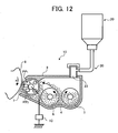
- FIG. 12 is a schematic drawing illustrating an exemplary construction of a development device 10 used in the above-described image forming apparatus.
- the development device 10 is arranged beside a photoconductor 8, and includes a non-magnetic development sleeve 7 serving as a developer bearing member bearing on a surface thereof a two-component developer including toner and magnetic carriers (hereinafter sometimes referred to simply as a developer).
- the development sleeve 7 is attached such that a part thereof exposes through an opening formed at a part of a development case at the side of the photoconductor 8, and is driven by a drive device (not shown) to rotate in the direction indicated by an arrow b in FIG. 12.
- a magnetic roller serving as a magnetic field generation device, which includes stationary magnets, is fixedly arranged inside of the development sleeve 7.
- the development device 10 also includes a doctor 9, which is a rigid body functioning as a developer regulation member for regulating a quantity of a developer born on the development sleeve 7.
- a developer accommodating part 4 accommodating the developer is formed at the upstream side in the rotating direction of the development sleeve 7 relative to the doctor 9, and first and second stirring screws 5 and 6 stirring and mixing the developer in the developer accommodating part 4 are provided in the developer accommodating part 4.
- a toner replenish opening 23 is arranged above the developer accommodating part 4, and a toner hopper 20 filled with toner to be replenished to the developer accommodating part 4 and a toner convey device 30 connecting the toner replenish opening 23 with the toner hopper 20 are provided.
- the first and second stirring screws 5 and 6 rotate, and thereby the developer in the developer accommodating part 4 is stirred and toner and magnetic carriers of the developer are charged by friction to respective polarities opposite to each other.
- the stirred developer is supplied to the periphery surface of the development sleeve 7, the supplied developer is born on the periphery surface of the development sleeve 7, and with rotation of the development sleeve 7 the developer born on the periphery surface of the development sleeve 7 is conveyed in the rotating direction (the arrow b direction) of the development sleeve 7.
- the developer born on the periphery surface of the development sleeve 7 is regulated in quantity by the doctor 9, and the developer born on the periphery surface o'f the development sleeve 7 after having been regulated in quantity is conveyed to a development area where the photoconductor 8 and the development sleeve 7 oppose each other.
- the toner in the developer electrostatically moves to a latent image on the surface of the photoconductor 8, and the latent image is visualized as a toner image.
- a magnetic carrier having a weight-average particle diameter of 20 ⁇ m or greater but not exceeding 60 ⁇ m is used.
- a trace of an ear and surface roughness in a half-tone image caused by the magnetic carrier can be prevented. That is, deterioration of an image in graininess can be prevented, and as a result, enhancement of an image quality can be realized.
- the particle diameter of the magnetic carrier 20 ⁇ m or greater mobility of the developer is prevented from being excessively deteriorated and stress to the developer is prevented from being excessively increased.
- a magnetic carrier is smaller in particle diameter, magnetization of the carrier is decreased, so that adhesion of the carrier to a photoconductor is easy to occur.
- a photoconductor having a diameter of 60mm or smaller is used, and for the development sleeve 7, a development sleeve having a diameter of 30mm or smaller is used.
- the magnetic holding force of a magnetic brush relative to carriers born on ear tips of the magnetic brush is decreased at a downstream (the exit side) of the development area, so that adhesion of the carriers to the photoconductor 8 is easy to occur. Due to occurrence of adhesion of carriers to the photoconductor 8, deterioration of the photoconductor 8 and members arranged to contact the photoconductor 8, such as a cleaning blade (not shown) for the photoconductor 8, etc., are accelerated, and a white spot caused by adhesion of carriers to the photoconductor 8 is generated in an image area.
- adhesion of the carrier to the photoconductor 8 is suppressed and at the same time an adverse effect, which may be caused when a countermeasure is taken for preventing adhesion of the carrier to the photoconductor 8, is suppressed within an allowable range.
- a magnetic carrier of the two-component developer for the magnetic carrier of the two-component developer, a magnetic carrier having the following characteristics is used.
- the saturation magnetization in a magnetic field of 1kOe is 66emu/g or greater but not exceeding 100emu/g, and the static resistance when a bias of 1000V has been applied is 10 9 ⁇ cm or greater but not exceeding 10 14 ⁇ cm.
- the carrier has a coating film including a bonding resin and particles, and a diameter D of the particles and a thickness h of the bonding resin film satisfies a relation: 1 ⁇ D/h ⁇ 10. Furthermore, only a DC bias is applied as the development bias and an AC bias is not applied.
- the magnetic holding force of a magnetic brush relative to the surface of the magnetic brush by the above-described magnetic roller serving as the magnetic field generation device is increased.
- the carrier is made hard to leave tips of the magnetic brush, so that adhesion of the carrier to the photoconductor 8 can be suppressed.
- saturation magnetization of the magnetic carrier in a magnetic field of 1kOe to 100emu/g or smaller ears of the magnetic brush are prevented from being excessively hardened to cause a trace of the ear tips to appear on an image.
- the static resistance of the magnetic carrier is set to be in a relatively low range, i.e., 10 9 ⁇ cm or greater but not exceeding 10 14 ⁇ cm.
- the static resistance and the saturation magnetization of a magnetic carrier have a certain correlation, and if the saturation magnetization is increased, the static resistance is decreased.
- the lower limit of the static resistance is set at 10 9 ⁇ cm.
- the saturation magnetization is set at 66emu/g or greater, it may occur that the static resistance is relatively high.
- the inventors of the present invention have found that if the static resistance is excessively high, a hollow image beyond an allowable range occurs. Therefore, the static resistance of the magnetic carrier is set at 10 14 ⁇ cm or smaller so that a hollow image is suppressed within the allowable range.
- a DC bias is applied to the development sleeve 7 by a power source 10 serving as a development electric field generation device connected with the development sleeve 7. That is, because the static resistance of the magnetic carrier is set relatively low as described above and thereby the magnetic carrier is easy to leak, applying an AC bias, that may cause leaking, is avoided so that leaking is hard to occur.
- a carrier having a relatively small particle diameter is used, and for preventing adhering of the carrier to a photoconductor, which is easy to occur due to the carrier having a relatively small particle diameter, saturation magnetization of the carrier is set relatively high. Further, for avoiding a spotted halftone image and a hollow image, that become easy to occur due to relatively high saturation magnetization of the carrier, from exceeding an allowable range, a range of static resistance of the magnetic carrier and a component of the development bias are specified.
- the image forming apparatus of the present invention is configured such that occurrence of density unevenness in a halftone image is suppressed to achieve a higher image quality.
- the width of a development gap which is a distance between the photoconductor 8 and the development sleeve 7 in the development area, has an effect on occurrence of density unevenness in a halftone image. If the development gap is too large, an electric field from the development sleeve 7 does not reach the photoconductor 8, so that a so-called turning over electric field is easy to be formed. In this case, toner does not adhere to an image area uniformly, and density unevenness occurs in particular in a halftone image.
- graininess of an image When density unevenness occurs in a halftone image, it is referred to as that graininess of an image has been deteriorated. Generally, when a spotted halftone image occurs, graininess of an image is deteriorated, however, it occurs that graininess of an image is deteriorated despite a spotted halftone image is not generated. Therefore, it is preferable that graininess of an image is made satisfactory for obtaining a higher quality image.
- the setting conditions of the full-color printer with respect to 5 examples of condition patterns of the present invention are as follows; Photoconductor linear velocity: 350mm/sec Photoconductor diameter: 60mm Development sleeve/photoconductor linear velocity ratio: 2 Developer scooping up quantity: 50mg/cm 2 Development sleeve diameter: 25mm Primary pole (PP1) angle: 6° Primary pole (PP1) magnetic flux density: 120mT Primary pole downstream side pole (PP2) magnetic flux density: 110mT Charge potential VD: -600V After exposure potential VL: -60V Development bias Vb: -430V
- the setting conditions of the full-color printer with respect to 17 comparative examples of condition patterns are as follows; Photoconductor linear velocity: 350mm/sec Photoconductor diameter: 60mm Development sleeve/photoconductor linear velocity ratio: 2 Developer scooping up quantity: 50mg/cm 2 Development sleeve diameter: 25mm Primary pole (PP1) angle: 6° Primary pole (PP1) magnetic flux density: 120mT Primary pole downstream side pole (PP2) magnetic flux density: 110mT Charge potential VD: -420V After exposure potential VL: -60V Development bias Vb: -250V
- a magnetic force distribution measure instrument (a three-dimensional magnetism measure instrument manufactured by EXCEL-SYSTEM, CO. LTD.) and a gauss meter (manufactured by AD-S, CO. LTD.) are used, and a sleeve-prodding method is used in measurement.
- the development sleeve 7 is the one processed with V-shaped grooving.
- the doctor 9 is made of a rigid and magnetic material.
- the doctor 9 may be constructed not only by a metal material such as steel and stainless but also by a resin material in which magnetic particles such as ferrite or magnetite are compounded. Further, instead of constructing the doctor 9 with a magnetic material, the doctor 9 may be constructed with a non-magnetic member, and a magnetic member such as a metal plate attached directly or indirectly to the non-magnetic member.
- Magnetic carriers used in the developer with respect to 5 examples of the present invention are obtained as described below.
- a coating film forming solution is blended.
- the coating film forming solution is applied to calcinated ferrite powder having a predetermined average particle diameter as a core member with a tumbled fluidized bed coater (SPIRA COTA manufactured by OKADA SEIKO, CO., LTD.) so that the thickness of a coating film is 0.15 ⁇ m.
- Carriers thus obtained are dehydrated and then are left in an electric furnace for 1 hour at 150°C to be calcinated. After cooling the calcinated carriers, a bulk of the ferrite powder is fragmented using a comb with a tooth-gap of 100 ⁇ m, and thereby the carriers are obtained.
- Magnetic carriers used in the developer with respect to 17 comparative examples are obtained as described below.
- a coating film forming solution is blended.
- the coating film forming solution is applied to calcinated ferrite powder having a predetermined average particle diameter as a core member with a tumbled fluidized bed coater (SPIRA COTA manufactured by OKADA SEIKO, CO., LTD.) so that the thickness of the coating film is 0.15 ⁇ m.
- Carriers thus obtained are hydrated and then are left in an electric furnace for 1 hour at 150°C to be calcinated. After cooling the calcinated carriers, a bulk of the ferrite powder is fragmented using a comb with a tooth-gap of 100 ⁇ m, and thereby the carriers are obtained.
- a coating film covering the surface of a carrier can be observed by observing a cross section of the carrier with a transmission electronic microscope. Therefore, a thickness of the coating film is obtained by averaging values of thickness of cross sections of the coating film thus observed.
- the coating film of the carriers used with respect to 17 comparative examples does not include particles. Accordingly, the ratio of the diameter D of particles included in the coating film of the carriers and the thickness h of the coating film described above with respect to the carriers used in relation to 5 examples of the present invention cannot be applied.
- Table 2 indicates the results of evaluation of image formation with respect to 5 examples of conditions patterns of the present invention, Examples E1 through E5, and 17 comparative examples of condition patterns, Comparative Examples CE1 through CE17.
- the evaluation has been made with respect to a spotted halftone image, a hollow image, graininess, and adhesion of carriers to a photoconductor.
- DC is specified in the column of bias, it indicates that only a DC bias has been applied as a development electric field
- AC is specified in the column of bias, it indicates that an AC bias has been superimposed on a DC bias.
- the AC bias is 4.5kHz in frequency, 0.9kV in Vpp, and 35 in duty.
- the development gap is labeled as PG.
- Saturation magnetization of carriers has been measured using a BHU-U type magnetization measure apparatus (manufactured by Riken Denshi. Co. Ltd.). About 1.0gr of a measuring sample is put in a cell 7mm in internal diameter and 10mm in height to be set in the measure apparatus. The applying magnetic field is gradually increased to 1kOe, and magnetization intensity in a magnetic field of 1kOe has been obtained.
- Comparative Example CE 10 satisfies the conditions of the present invention, but is listed as a comparative example.
- adhesion of carriers to a photoconductor is easy to be effected by saturation magnetization of the carriers, and adhesion of carriers to a photoconductor has occurred in Comparative Examples CE6, CE9, CE12 and CE15 in which the saturation magnetization of carriers is smaller than 66. Adhesion of carriers to a photoconductor also has occurred in Comparative Examples CE11 and CE17 in which the static resistance of carriers is low at 10 8 ⁇ cm. Thus, occurrence of adhesion of carriers to a photoconductor depends on saturation magnetization and in some cases on static resistance of carriers.
- a spotted halftone image is easy to occur when an AC bias is applied as the development bias, and has occurred in Examples E1-E5 in which a superimposed bias has been applied.
- Comparative Examples CE 12 and CE15 in which the saturation magnetization of carriers is relatively small, even when a superimposed bias has been used, a spotted halftone image has not occurred.
- Comparative Examples CE12 and CE15 as described above, adhesion of carriers to a photoconductor has occurred, which is undesirable.
- occurrence of a spotted halftone image is easy to be affected by static resistance of magnetic carriers, and in Comparative Examples CE 11 and CE17 in which the static resistance of carriers is low as 10 8 ⁇ cm, a spotted halftone image has occurred despite that only a DC bias has been applied as the development bias.
- FIG. 13 is a diagram of a graph indicating a result of investigating a difference in a relation of saturation magnetization of magnetic carriers and occurrence of a spotted halftone image between a case A in which the saturation magnetization of magnetic carriers has been set relatively high at 70emu/g and a case B in which the saturation magnetization of magnetic carriers has been set relatively low at 60emu/g.
- a superimposed bias has been applied, and real resistance of the magnetic carriers has been measured at intervals of 200V.
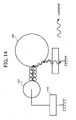
- FIG. 14 illustrates a schematic construction of a real resistance measurement instrument used in measurement, and as illustrated FIG. 14, a bias is applied to a development sleeve 107 from a power source 110 and thereby a magnetic brush is formed.
- a jig photoconductor 108 made of aluminum is used as a photoconductor opposing the development sleeve 107, and the distance between the development sleeve 107 and the photoconductor 108 is 0.35mm.
- the development sleeve 107 is rotated, and a DC bias is applied to the development sleeve 107.
- an electric current flowed into the jig photoconductor 108 is measured by a multi-meter to be converted to a resistance value.
- Table 3 indicates a result of measurement of real resistance of magnetic carriers with respect to the cases A and B. Applying Voltage (V) 100 200 400 600 800 1000 1200 1400 Case A 7.9 9.1 9.9 10.3 8.6 BD Case B 8.1 9.1 9.6 9.9 9.3 8.7 8.0 BD
- real resistance of magnetic carriers changes depending upon saturation magnetization of the magnetic carriers.
- a state that real resistance of magnetic carriers cannot be measured i.e., a breakdown state
- a breakdown state is a state wherein real resistance of carriers is so low that a large current that cannot be measured flows.
- BD indicates that a breakdown state has occurred. Also, it has been confirmed by visual observation that by increasing saturation magnetization of carriers, each of magnetic brush bristles becomes thick and short.
- static resistance of a carrier is a resistance value measured in a state that the carrier is packed in a cell.
- the resistance value is a value measured by a high-resistance measure instrument after a magnetic carrier has been placed between resistance measurement parallel electrodes having a gap of 2mm, 30sec after applying a DC bias, and then converted to volume resistivity.
- static resistance of a magnetic carrier when static resistance of a magnetic carrier is too low, a spotted halftone image may be caused, and adhesion of the carrier to a photoconductor due to charge injection may occur.
- static resistance of the carrier when static resistance of the carrier is too high, an inferior image such as a hollow image, etc. may get worse.
- static resistance of a carrier is preferably made low as much as possible.
- an AC bias when an AC bias is applied, because the applying voltage is relatively large, a lower limit of a setting range of static resistance values must be increased as compared with a case of applying only a DC bias.
- static resistance of carriers can be set relatively low as compared with a case of applying an AC bias, so that it becomes possible to set the static resistance of the carriers such that an inferior image such as a hollow image, etc. will not exceed an allowable range.
- the development gap PG which is a gap between the photoconductor 8 and the development sleeve 7 in the development area.
- a development electric field does not reach the photoconductor 8 from the development sleeve 7, so that a so-called returning electric field in which the development electric field returns to a surface of the development sleeve 7 is caused.
- toner does not adhere to an image area on the photoconductor 8 uniformly, and in particular, graininess of a halftone image is deteriorated.
- the development gap PG is set relatively small, i.e., 0.4mm or smaller. It is known that making the development gap PG smaller improves a hollow image and a solid/line toner adhesion ratio (a ratio between quantities of toner adhesion in a solid image area and a line image area), etc. However, if the development gap PG is made too small, slight variation in the development gap PG may cause the development sleeve 7 and the photoconductor 8 to contact each other while sandwiching a developer, or toner sandwiched between them may be caused to fixedly adhere to the development sleeve 7. In Examples E1 through E5 of the present invention, the lower limit of the development gap PG is set at 0.2mm, which is a generally set lower limit value.
- the development gap PG is set relatively large at 0. 5mm, and evaluation results with respect to graininess of an image are extremely unsatisfactory, respectively. Generally, when a spotted halftone image occurs, graininess of an image is also deteriorated. In Examples E1 through E5 of the present invention, the development gap PG is 0.2mm or greater but not exceeding 0.4mm, and thereby a development electric field uniformly reaches an image area on the photoconductor 8, so that graininess of an image is satisfactory, respectively. Graininess of an image is also related to particle diameters of magnetic carriers and toner, and when such toner having a relatively small particle diameter is used as in the embodiment of the present invention, the graininess of an image is further improved.
- a carrier having a coating film including at least a bonding resin and particles and in which the relation of 1 ⁇ D/h ⁇ 10 between a diameter D of the particles and a thickness h of a film of the bonding resin is satisfied has been used.
- quantity of the developer held at the upstream side of the doctor 9 (the upstream side in the rotation direction of the development sleeve 7) is increased, so that extremely high stress is given to the developer. Therefore, scraping of a carrier coating film, contamination of surfaces of the carriers due to adhesion of melted toner, etc., occur, so that a life of the developer is decreased.
- the particles are relatively convex as compared with the bonding resin film. Therefore, in stirring a developer including the carriers and toner so that the developer is charged by friction, contacting of the carriers with each other or with toner, which is accompanied by a strong shock against the bonding resin film due to friction between the carriers or with the toner, is mitigated. Thereby, scraping of the bonding resin film where charging occurs, and contamination of the carriers due to toner adhesion can be prevented, so that the life of the carriers can be greatly enhanced.
- the ratio of D/h is 1 or smaller, the particles are buried in the bonding resin film, so that the effect of adding the particles is greatly decreased, which is not desirable.
- the ratio of D/h is 10 or greater, the contacting area between the particle and the bonding resin film is relatively small, so that a sufficient holding force cannot be obtained and the particle is easy to be detached from the bonding resin film, which is also undesirable.
- a doctor having rigidity and magnetization is used for improving the charge rising characteristic of toner, the above-described effect on improving a magnetic carrier life is greater because when a magnetic doctor is used, the quantity of a developer held at the doctor is increased and thereby a stress given to the developer is excessively large.
- the magnetic doctor may be constructed not only by a metal material such as steel and stainless, but also by a resin material in which a magnetic particle such as ferrite or magnetite is compounded.
- the doctor may be constructed with a non-magnetic member and a magnetic member such as a metal plate attached to the non-magnetic member directly or indirectly, and thereby substantially the same effect on improving a carrier life as described above can be obtained.
- FIG. 15 is a diagram of a graph indicating changes in charge amount over the number of images (prints) produced by the printer, with respect to a carrier C1 of Examples E1-E5 satisfying the above-described relation of 1 ⁇ D/h ⁇ 10 and a carrier C2 of Comparative Examples CE1-CE17.
- decreasing ratios relative to a charge amount of 1 when starting printing images are indicated.
- the charge amount is caused to decrease by excessive adhesion of toner to carriers, etc. while the prints are made.
- the charge amount is 0.8 or smaller, i.e., when the decreasing ratio exceeds 20%, an inferior image starts to occur.
- the charge amount of the carrier C1 is greater than 0.8 even when the number of prints exceeds 100,000.
- the charge amount of the carrier C2 is 0.8 or smaller before the number of prints reaches 100,000. From this, it can be said that the carrier of the present invention, that has a coating film including at least a bonding resin and particles and that satisfies the relation of 1 ⁇ D/h ⁇ 10 wherein D is a diameter of the particles and h is a thickness of a film of the bonding resin, can suppress decrease in charge amount due to excessive adhesion of toner to the carriers.
- the upper limit of the value of D/h is preferably 5 from the aspect of preventing detachment of the particles from the film of the bonding resin.
- the average particle diameter by weight of magnetic carriers is 20 ⁇ m or greater but not exceeding 60 ⁇ m
- the saturation magnetization of the carriers is 66emu/g or greater but not exceeding 100emu/g
- the static resistance of the carriers when 100V is applied is 10 9 ⁇ cm or greater but not exceeding 10 14 ⁇ cm.
- only a DC bias is applied as the development bias.
- the magnetic flux density of the primary pole PP1 is 120mT, and the magnetic flux density of the pole PP2 at the downstream side of the primary pole PP1 is 110mT.
- those magnetic flux densities are not limited to those values, and the advantages of the present invention can be obtained if the magnetic flux densities of respective poles are greater than the above-described values.
- the development gap PG is made 0.2mm or greater but not exceeding 0.4mm, and thereby graininess of an image is satisfactory.
- a carrier having a coating film including at least a bonding resin and particles and satisfying the relation of 1 ⁇ D/h ⁇ 10 wherein D is a diameter of the particles and h is a thickness of a film of the bonding resin is used.
Landscapes
- Physics & Mathematics (AREA)
- General Physics & Mathematics (AREA)
- Developing Agents For Electrophotography (AREA)
- Magnetic Brush Developing In Electrophotography (AREA)
- Dry Development In Electrophotography (AREA)
Applications Claiming Priority (4)
| Application Number | Priority Date | Filing Date | Title |
|---|---|---|---|
| JP2002380935 | 2002-12-27 | ||
| JP2002380935A JP2004212560A (ja) | 2002-12-27 | 2002-12-27 | 画像形成装置 |
| JP2003051489A JP2004258524A (ja) | 2003-02-27 | 2003-02-27 | 磁性キャリア、二成分現像剤、現像方法、現像装置、画像形成装置 |
| JP2003051489 | 2003-02-27 |
Publications (2)
| Publication Number | Publication Date |
|---|---|
| EP1434104A2 true EP1434104A2 (de) | 2004-06-30 |
| EP1434104A3 EP1434104A3 (de) | 2004-11-17 |
Family
ID=32473758
Family Applications (1)
| Application Number | Title | Priority Date | Filing Date |
|---|---|---|---|
| EP03029279A Withdrawn EP1434104A3 (de) | 2002-12-27 | 2003-12-22 | Magnetischer Träger, Zweikomponentenentwickler, Entwicklungsverfahren, Entwicklungsgerät und elektrophotographischer Apparat zur Bildherstellung |
Country Status (3)
| Country | Link |
|---|---|
| US (2) | US7020421B2 (de) |
| EP (1) | EP1434104A3 (de) |
| CN (1) | CN100428069C (de) |
Families Citing this family (15)
| Publication number | Priority date | Publication date | Assignee | Title |
|---|---|---|---|---|
| US6631247B1 (en) | 1999-09-29 | 2003-10-07 | Ricoh Co., Ltd. | Method and system for remote diagnostic, control and information collection based on various communication modes for sending messages to a resource manager |
| JP2004271876A (ja) * | 2003-03-07 | 2004-09-30 | Ricoh Co Ltd | 現像剤担持体、現像方法、現像装置、プロセスカートリッジ及び画像形成装置 |
| JP4087324B2 (ja) * | 2003-10-10 | 2008-05-21 | 株式会社リコー | 静電潜像現像剤用キャリア、現像剤、現像装置、現像剤容器、画像形成装置、現像方法及びプロセスカートリッジ |
| JP4708252B2 (ja) * | 2006-04-20 | 2011-06-22 | 株式会社リコー | 画像形成装置 |
| JP5207702B2 (ja) * | 2006-10-20 | 2013-06-12 | キヤノン株式会社 | 画像形成装置 |
| JP5392593B2 (ja) | 2007-10-23 | 2014-01-22 | 株式会社リコー | 画像形成装置 |
| JP5370800B2 (ja) * | 2007-10-26 | 2013-12-18 | 株式会社リコー | 画像形成装置および現像剤充填方法 |
| JP4610603B2 (ja) * | 2007-12-28 | 2011-01-12 | シャープ株式会社 | トナー、二成分現像剤、現像装置および画像形成装置 |
| JP5492398B2 (ja) * | 2008-01-10 | 2014-05-14 | 株式会社リコー | 画像形成装置 |
| JP5403393B2 (ja) * | 2008-03-28 | 2014-01-29 | 株式会社リコー | 現像装置並びにこれを備える画像形成装置及びプロセスカートリッジ |
| JP5240550B2 (ja) * | 2008-03-31 | 2013-07-17 | 株式会社リコー | 現像装置並びにこれを備える画像形成装置及びプロセスカートリッジ |
| JP5429587B2 (ja) | 2008-04-01 | 2014-02-26 | 株式会社リコー | 現像装置並びにこれを備える画像形成装置及びプロセスカートリッジ |
| JP2012208473A (ja) * | 2011-03-11 | 2012-10-25 | Ricoh Co Ltd | 現像装置、画像形成装置、画像形成方法及びプロセスカートリッジ |
| JP5900056B2 (ja) * | 2011-06-08 | 2016-04-06 | 株式会社リコー | 画像形成装置 |
| JP2013167850A (ja) * | 2012-02-17 | 2013-08-29 | Canon Inc | 画像形成装置、画像形成装置の評価方法、およびパラメータ測定方法 |
Family Cites Families (76)
| Publication number | Priority date | Publication date | Assignee | Title |
|---|---|---|---|---|
| JPS54155048A (en) | 1978-05-29 | 1979-12-06 | Ricoh Co Ltd | Carrier material for electrophotographic development |
| JPS5740267A (en) | 1980-08-22 | 1982-03-05 | Canon Inc | Coated carrier for electrophotographic developing |
| US4406536A (en) * | 1981-02-04 | 1983-09-27 | Ricoh Company, Ltd. | Developing device |
| JPS58108548A (ja) | 1981-12-22 | 1983-06-28 | Canon Inc | 電子写真用キヤリア− |
| JPS58108549A (ja) | 1981-12-22 | 1983-06-28 | Canon Inc | 電子写真用キヤリア− |
| JPS5994763A (ja) * | 1982-11-22 | 1984-05-31 | Mita Ind Co Ltd | 磁気ブラシ現像用二成分系現像剤 |
| US4540645A (en) * | 1983-01-31 | 1985-09-10 | Mita Industrial Co Ltd | Magnetic brush development method |
| JPS59166968A (ja) | 1983-03-11 | 1984-09-20 | Canon Inc | 被覆キヤリヤ− |
| US4601967A (en) * | 1983-12-10 | 1986-07-22 | Ricoh Company, Ltd. | Toner particles having a relatively high specific volume resistivity coating layer |
| GB2186818B (en) * | 1986-02-20 | 1990-07-11 | Ricoh Kk | Developing electrostatic latent images |
| FR2597625B1 (fr) * | 1986-04-18 | 1992-02-14 | Ricoh Kk | Appareil pour developper une image electrostatique latente, notamment en electrocopie |
| GB2194179B (en) * | 1986-04-24 | 1990-03-14 | Ricoh Kk | Rotary multicolor developing apparatus |
| JPS63292163A (ja) * | 1987-05-26 | 1988-11-29 | Ricoh Co Ltd | 画像形成装置 |
| JPS6419584A (en) | 1987-07-15 | 1989-01-23 | Hitachi Ltd | Semiconductor memory device |
| JPS6419584U (de) | 1987-07-28 | 1989-01-31 | ||
| JP2746885B2 (ja) | 1987-09-28 | 1998-05-06 | 株式会社東芝 | 画像形成装置 |
| GB2212419B (en) * | 1987-12-25 | 1991-12-04 | Ricoh Kk | Image density control method and color image forming apparatus |
| US4989043A (en) * | 1988-05-09 | 1991-01-29 | Ricoh Company, Ltd. | Color-balance control method |
| JP2683624B2 (ja) | 1988-09-16 | 1997-12-03 | 三田工業株式会社 | プロセスユニット |
| US5298944A (en) * | 1989-06-30 | 1994-03-29 | Ricoh Company, Ltd. | Testing image density to control toner concentration and dynamic range in a digital copier |
| FR2653241B1 (fr) * | 1989-10-13 | 1994-03-11 | Ricoh Cy Ltd | Procede de developpement et appareil associe utilisant un support de revelateur qui peut former des micro-champs a sa surface. |
| US5674408A (en) * | 1990-03-24 | 1997-10-07 | Ricoh Company, Ltd. | Developer carrier capable of forming microfields thereon and method of producing the same |
| JPH03628A (ja) | 1990-03-30 | 1991-01-07 | Sanyo Electric Co Ltd | 薬剤包装機 |
| US5172169A (en) * | 1990-04-09 | 1992-12-15 | Ricoh Company, Ltd. | Developer carrier of a developing device and a method of producing the same |
| JP3090485B2 (ja) * | 1990-04-26 | 2000-09-18 | 株式会社リコー | トナー |
| GB2244350B (en) * | 1990-04-27 | 1994-08-10 | Ricoh Kk | Image forming method and apparatus for the same |
| JP2627689B2 (ja) * | 1990-06-14 | 1997-07-09 | 株式会社リコー | 現像装置 |
| US5741616A (en) * | 1990-06-14 | 1998-04-21 | Ricoh Company, Ltd. | Method of developing latent electrostatic images and developer-bearing member |
| US5293198A (en) * | 1990-08-10 | 1994-03-08 | Ricoh Company, Ltd. | Image forming apparatus for controlling the dynamic range of an image |
| JPH04270356A (ja) * | 1990-08-10 | 1992-09-25 | Ricoh Co Ltd | 画像形成装置 |
| DE4128942C2 (de) * | 1991-01-16 | 1995-06-22 | Ricoh Kk | Entwicklungseinrichtung, welche in einer Bilderzeugungseinrichtung vorgesehen ist |
| JP3310685B2 (ja) * | 1991-03-20 | 2002-08-05 | 株式会社リコー | 画像形成装置 |
| JP3120460B2 (ja) | 1991-03-28 | 2000-12-25 | 富士ゼロックス株式会社 | 電子写真用現像剤 |
| US5220383A (en) * | 1991-04-01 | 1993-06-15 | Ricoh Company, Ltd. | Developing device for an image forming apparatus having a large number of microfields formed on a developer carrier |
| US5245391A (en) * | 1991-04-01 | 1993-09-14 | Ricoh Company, Ltd. | Developing device having surface microfields for an image forming apparatus |
| JPH05216337A (ja) * | 1991-07-31 | 1993-08-27 | Ricoh Co Ltd | 画像形成装置 |
| JP2995949B2 (ja) | 1991-09-09 | 1999-12-27 | 富士ゼロックス株式会社 | 電子写真用現像剤 |
| JP3243696B2 (ja) * | 1991-11-14 | 2002-01-07 | 株式会社リコー | 現像装置 |
| US5384628A (en) | 1992-10-10 | 1995-01-24 | Ricoh Company, Ltd. | Developing device for image forming equipment |
| JPH06202381A (ja) | 1993-01-05 | 1994-07-22 | Minolta Camera Co Ltd | 静電潜像用現像剤 |
| JP3305033B2 (ja) | 1993-02-26 | 2002-07-22 | 株式会社リコー | 現像装置 |
| US5508794A (en) | 1993-03-03 | 1996-04-16 | Ricoh Company, Ltd. | Developer recycling system and developer cartridge therefor |
| DE69425624T2 (de) | 1993-10-15 | 2001-04-26 | Canon K.K., Tokio/Tokyo | Trägermaterial für Elektrophotographie, Entwickler des zwei-komponenten Typs, und Bildherstellungsverfahren |
| JPH07225520A (ja) | 1993-12-16 | 1995-08-22 | Ricoh Co Ltd | 画像形成装置 |
| JP3397483B2 (ja) | 1993-12-29 | 2003-04-14 | キヤノン株式会社 | 電子写真用キャリア,その製造方法,二成分系現像剤及び画像形成方法 |
| JPH086307A (ja) | 1994-06-16 | 1996-01-12 | Fuji Xerox Co Ltd | 電子写真用キャリア及びその製造方法、並びに電子写真用帯電付与部材 |
| JP3413314B2 (ja) | 1994-10-21 | 2003-06-03 | 株式会社リコー | 画像形成装置 |
| JPH08179618A (ja) | 1994-12-21 | 1996-07-12 | Ricoh Co Ltd | 画像形成装置 |
| JPH08305159A (ja) | 1995-04-28 | 1996-11-22 | Ricoh Co Ltd | 画像形成装置 |
| JP3516551B2 (ja) | 1995-05-11 | 2004-04-05 | 株式会社リコー | 静電画像形成装置 |
| US5819145A (en) | 1995-07-31 | 1998-10-06 | Ricoh Company, Ltd. | Image forming device for forming a uniform toner layer on a developing roller |
| US5697031A (en) * | 1995-08-04 | 1997-12-09 | Ricoh Company, Ltd. | Image forming apparatus and method for overlaid transfer of images |
| JP3605707B2 (ja) | 1995-10-11 | 2004-12-22 | 株式会社リコー | 画像形成装置 |
| JPH09160304A (ja) | 1995-12-13 | 1997-06-20 | Fuji Xerox Co Ltd | 静電潜像現像剤用キャリア及びそれを用いた静電潜像現像剤並びに画像形成方法 |
| JP3500008B2 (ja) | 1996-05-28 | 2004-02-23 | 株式会社リコー | 画像形成装置における現像能力検知方法 |
| JPH1055113A (ja) | 1996-08-09 | 1998-02-24 | Fuji Xerox Co Ltd | 画像形成装置 |
| JPH10254310A (ja) * | 1996-11-29 | 1998-09-25 | Ricoh Co Ltd | 画像形成装置 |
| US5983060A (en) | 1997-03-31 | 1999-11-09 | Ricoh Company, Ltd. | Image forming apparatus which removes a surface potential of an intermediate transfer member |
| JP3562787B2 (ja) * | 1998-01-08 | 2004-09-08 | パウダーテック株式会社 | 電子写真現像剤用フェライトキャリア及び該キャリアを用いた電子写真現像剤 |
| CN100507729C (zh) | 1998-04-20 | 2009-07-01 | 株式会社理光 | 图像形成装置及方法 |
| US6226481B1 (en) | 1998-12-07 | 2001-05-01 | Ricoh Company, Ltd. | Image forming apparatus with control over developing unit during an idle running of an intermediate image transfer body |
| JP3497396B2 (ja) * | 1998-12-24 | 2004-02-16 | 京セラミタ株式会社 | 静電潜像現像用キャリア及び静電潜像現像剤 |
| JP4251468B2 (ja) | 1999-07-15 | 2009-04-08 | 株式会社リコー | 二成分現像剤および画像形成装置 |
| JP3942139B2 (ja) | 1999-10-20 | 2007-07-11 | 株式会社リコー | 電子写真用現像剤 |
| JP2001242712A (ja) | 2000-02-28 | 2001-09-07 | Ricoh Co Ltd | 画像形成装置 |
| JP2001242696A (ja) * | 2000-02-28 | 2001-09-07 | Bridgestone Corp | 現像剤担持体及びそれを用いた画像形成装置 |
| JP2001324862A (ja) | 2000-05-15 | 2001-11-22 | Fuji Xerox Co Ltd | 画像形成装置 |
| US6597885B2 (en) | 2000-06-05 | 2003-07-22 | Ricoh Company, Ltd. | Image forming apparatus having a developing device with a magnet brush |
| US6597881B2 (en) | 2000-10-16 | 2003-07-22 | Ricoh Company, Ltd. | Image forming apparatus |
| JP2002139885A (ja) | 2000-11-01 | 2002-05-17 | Ricoh Co Ltd | 画像形成装置 |
| JP2002207324A (ja) | 2001-01-09 | 2002-07-26 | Konica Corp | 電子写真用キャリアとその製造方法、電子写真用現像剤及び画像形成方法 |
| US6701100B2 (en) | 2001-01-23 | 2004-03-02 | Ricoh Company, Ltd. | Image forming apparatus including an image carrier and a polarization uniforming structure |
| JP3966536B2 (ja) | 2001-01-29 | 2007-08-29 | 株式会社リコー | 電子写真現像剤用キャリア及び現像剤 |
| JP2003084574A (ja) * | 2001-03-16 | 2003-03-19 | Ricoh Co Ltd | 現像方法、現像装置及び画像形成方法 |
| US6882818B2 (en) | 2001-03-21 | 2005-04-19 | Ricoh Company, Ltd. | Image forming apparatus having a development apparatus forming a magnetic brush separated from a latent image carrier outside a development area |
| JP2002296846A (ja) * | 2001-03-30 | 2002-10-09 | Powdertech Co Ltd | 電子写真現像剤用キャリア及び該キャリアを用いた現像剤 |
-
2003
- 2003-12-22 EP EP03029279A patent/EP1434104A3/de not_active Withdrawn
- 2003-12-29 US US10/746,060 patent/US7020421B2/en not_active Expired - Fee Related
- 2003-12-29 CN CNB2003101242777A patent/CN100428069C/zh not_active Expired - Fee Related
-
2005
- 2005-08-24 US US11/209,770 patent/US7474867B2/en not_active Expired - Fee Related
Also Published As
| Publication number | Publication date |
|---|---|
| US20040190946A1 (en) | 2004-09-30 |
| US7020421B2 (en) | 2006-03-28 |
| US20050281593A1 (en) | 2005-12-22 |
| CN100428069C (zh) | 2008-10-22 |
| EP1434104A3 (de) | 2004-11-17 |
| CN1512276A (zh) | 2004-07-14 |
| US7474867B2 (en) | 2009-01-06 |
Similar Documents
| Publication | Publication Date | Title |
|---|---|---|
| US7474867B2 (en) | Magnetic carrier, two-component developer, development method, development device and image forming apparatus of electrophotography | |
| US6898406B2 (en) | Developing device having a developer forming a magnet brush | |
| US4254203A (en) | Dry process developing method employing magnetic toner | |
| US6708015B2 (en) | Developing device and image forming apparatus using the same | |
| JP2001272857A (ja) | 現像装置、画像形成装置及び画像形成プロセスユニット | |
| EP0212669B1 (de) | Entwicklungsverfahren für ein latentes elektrostatisches Bild | |
| US5428428A (en) | Developing device having a control electrode | |
| US7142804B2 (en) | Toner, toner cartridge that holds the toner therein, and image forming apparatus into which the toner cartridge is attached | |
| US5554479A (en) | Image formation method | |
| US11693350B2 (en) | Image forming apparatus | |
| JPH0293671A (ja) | 現像方法 | |
| JP7687103B2 (ja) | 現像装置およびそれを備えた画像形成装置 | |
| JP2006091425A (ja) | 現像装置及びそれを用いた電子写真装置 | |
| JPS5895748A (ja) | 転写型磁性トナ−粒子 | |
| JP2004258524A (ja) | 磁性キャリア、二成分現像剤、現像方法、現像装置、画像形成装置 | |
| JPH0279863A (ja) | 現像方法 | |
| JP2000206794A (ja) | 画像形成装置 | |
| JP3363604B2 (ja) | 画像形成装置 | |
| JP2004029254A (ja) | 現像装置及び画像形成装置 | |
| JP2000347507A (ja) | 現像装置 | |
| JPS62192756A (ja) | 現像方法 | |
| JP2003215927A (ja) | 画像形成装置 | |
| JPS63228176A (ja) | 静電像現像方法及びそれを実施する装置 | |
| JPH041677A (ja) | 現像装置 | |
| JPH04310985A (ja) | 現像装置 |
Legal Events
| Date | Code | Title | Description |
|---|---|---|---|
| PUAI | Public reference made under article 153(3) epc to a published international application that has entered the european phase |
Free format text: ORIGINAL CODE: 0009012 |
|
| AK | Designated contracting states |
Kind code of ref document: A2 Designated state(s): AT BE BG CH CY CZ DE DK EE ES FI FR GB GR HU IE IT LI LU MC NL PT RO SE SI SK TR |
|
| AX | Request for extension of the european patent |
Extension state: AL LT LV MK |
|
| 17P | Request for examination filed |
Effective date: 20040803 |
|
| PUAL | Search report despatched |
Free format text: ORIGINAL CODE: 0009013 |
|
| AK | Designated contracting states |
Kind code of ref document: A3 Designated state(s): AT BE BG CH CY CZ DE DK EE ES FI FR GB GR HU IE IT LI LU MC NL PT RO SE SI SK TR |
|
| AX | Request for extension of the european patent |
Extension state: AL LT LV MK |
|
| 17Q | First examination report despatched |
Effective date: 20050216 |
|
| AKX | Designation fees paid |
Designated state(s): DE ES FR GB IT NL |
|
| STAA | Information on the status of an ep patent application or granted ep patent |
Free format text: STATUS: THE APPLICATION HAS BEEN WITHDRAWN |
|
| 18W | Application withdrawn |
Effective date: 20090525 |