EP1426461B1 - Mask for coating by vacuum evaporation - Google Patents
Mask for coating by vacuum evaporation Download PDFInfo
- Publication number
- EP1426461B1 EP1426461B1 EP03257499A EP03257499A EP1426461B1 EP 1426461 B1 EP1426461 B1 EP 1426461B1 EP 03257499 A EP03257499 A EP 03257499A EP 03257499 A EP03257499 A EP 03257499A EP 1426461 B1 EP1426461 B1 EP 1426461B1
- Authority
- EP
- European Patent Office
- Prior art keywords
- apertures
- mask
- dummy
- organic
- evaporation mask
- Prior art date
- Legal status (The legal status is an assumption and is not a legal conclusion. Google has not performed a legal analysis and makes no representation as to the accuracy of the status listed.)
- Expired - Lifetime
Links
- 238000007738 vacuum evaporation Methods 0.000 title description 2
- 239000011248 coating agent Substances 0.000 title 1
- 238000000576 coating method Methods 0.000 title 1
- 238000001704 evaporation Methods 0.000 claims description 161
- 230000008020 evaporation Effects 0.000 claims description 155
- 239000010408 film Substances 0.000 claims description 68
- 238000000034 method Methods 0.000 claims description 41
- 239000000758 substrate Substances 0.000 claims description 33
- 230000008021 deposition Effects 0.000 claims description 22
- 239000000463 material Substances 0.000 claims description 14
- 238000004519 manufacturing process Methods 0.000 claims description 13
- 230000008569 process Effects 0.000 claims description 9
- 238000007789 sealing Methods 0.000 claims description 9
- 239000011368 organic material Substances 0.000 claims description 4
- 239000010409 thin film Substances 0.000 claims description 2
- 238000000151 deposition Methods 0.000 description 24
- 238000000059 patterning Methods 0.000 description 21
- 239000012212 insulator Substances 0.000 description 9
- 238000003466 welding Methods 0.000 description 9
- 239000000853 adhesive Substances 0.000 description 6
- 230000000052 comparative effect Effects 0.000 description 6
- 230000005525 hole transport Effects 0.000 description 6
- 229910052751 metal Inorganic materials 0.000 description 6
- 239000002184 metal Substances 0.000 description 6
- PXHVJJICTQNCMI-UHFFFAOYSA-N Nickel Chemical compound [Ni] PXHVJJICTQNCMI-UHFFFAOYSA-N 0.000 description 5
- 230000015572 biosynthetic process Effects 0.000 description 5
- 238000005530 etching Methods 0.000 description 5
- 229910052759 nickel Inorganic materials 0.000 description 3
- XLYOFNOQVPJJNP-UHFFFAOYSA-N water Substances O XLYOFNOQVPJJNP-UHFFFAOYSA-N 0.000 description 3
- 229910000531 Co alloy Inorganic materials 0.000 description 2
- VYPSYNLAJGMNEJ-UHFFFAOYSA-N Silicium dioxide Chemical compound O=[Si]=O VYPSYNLAJGMNEJ-UHFFFAOYSA-N 0.000 description 2
- 230000001070 adhesive effect Effects 0.000 description 2
- 229910052782 aluminium Inorganic materials 0.000 description 2
- XAGFODPZIPBFFR-UHFFFAOYSA-N aluminium Chemical compound [Al] XAGFODPZIPBFFR-UHFFFAOYSA-N 0.000 description 2
- 239000011575 calcium Substances 0.000 description 2
- 230000008859 change Effects 0.000 description 2
- 238000006243 chemical reaction Methods 0.000 description 2
- 239000010941 cobalt Substances 0.000 description 2
- GUTLYIVDDKVIGB-UHFFFAOYSA-N cobalt atom Chemical compound [Co] GUTLYIVDDKVIGB-UHFFFAOYSA-N 0.000 description 2
- 238000001816 cooling Methods 0.000 description 2
- 230000008878 coupling Effects 0.000 description 2
- 238000010168 coupling process Methods 0.000 description 2
- 238000005859 coupling reaction Methods 0.000 description 2
- 238000005323 electroforming Methods 0.000 description 2
- 239000007788 liquid Substances 0.000 description 2
- 239000000696 magnetic material Substances 0.000 description 2
- 238000005192 partition Methods 0.000 description 2
- 238000000206 photolithography Methods 0.000 description 2
- 229920002120 photoresistant polymer Polymers 0.000 description 2
- 230000004044 response Effects 0.000 description 2
- MBPCKEZNJVJYTC-UHFFFAOYSA-N 4-[4-(n-phenylanilino)phenyl]aniline Chemical compound C1=CC(N)=CC=C1C1=CC=C(N(C=2C=CC=CC=2)C=2C=CC=CC=2)C=C1 MBPCKEZNJVJYTC-UHFFFAOYSA-N 0.000 description 1
- OYPRJOBELJOOCE-UHFFFAOYSA-N Calcium Chemical compound [Ca] OYPRJOBELJOOCE-UHFFFAOYSA-N 0.000 description 1
- VYZAMTAEIAYCRO-UHFFFAOYSA-N Chromium Chemical compound [Cr] VYZAMTAEIAYCRO-UHFFFAOYSA-N 0.000 description 1
- 229910000990 Ni alloy Inorganic materials 0.000 description 1
- 239000004642 Polyimide Substances 0.000 description 1
- QXZUUHYBWMWJHK-UHFFFAOYSA-N [Co].[Ni] Chemical compound [Co].[Ni] QXZUUHYBWMWJHK-UHFFFAOYSA-N 0.000 description 1
- 230000002411 adverse Effects 0.000 description 1
- 229910045601 alloy Inorganic materials 0.000 description 1
- 239000000956 alloy Substances 0.000 description 1
- 229910052791 calcium Inorganic materials 0.000 description 1
- 230000015556 catabolic process Effects 0.000 description 1
- 229910017052 cobalt Inorganic materials 0.000 description 1
- 229910052681 coesite Inorganic materials 0.000 description 1
- 238000004040 coloring Methods 0.000 description 1
- XCJYREBRNVKWGJ-UHFFFAOYSA-N copper(II) phthalocyanine Chemical compound [Cu+2].C12=CC=CC=C2C(N=C2[N-]C(C3=CC=CC=C32)=N2)=NC1=NC([C]1C=CC=CC1=1)=NC=1N=C1[C]3C=CC=CC3=C2[N-]1 XCJYREBRNVKWGJ-UHFFFAOYSA-N 0.000 description 1
- 229910052906 cristobalite Inorganic materials 0.000 description 1
- 238000005520 cutting process Methods 0.000 description 1
- 230000007423 decrease Effects 0.000 description 1
- 230000007547 defect Effects 0.000 description 1
- 238000006731 degradation reaction Methods 0.000 description 1
- 230000000593 degrading effect Effects 0.000 description 1
- 230000000694 effects Effects 0.000 description 1
- 238000002474 experimental method Methods 0.000 description 1
- 238000001914 filtration Methods 0.000 description 1
- 239000011521 glass Substances 0.000 description 1
- 238000010438 heat treatment Methods 0.000 description 1
- RBTKNAXYKSUFRK-UHFFFAOYSA-N heliogen blue Chemical compound [Cu].[N-]1C2=C(C=CC=C3)C3=C1N=C([N-]1)C3=CC=CC=C3C1=NC([N-]1)=C(C=CC=C3)C3=C1N=C([N-]1)C3=CC=CC=C3C1=N2 RBTKNAXYKSUFRK-UHFFFAOYSA-N 0.000 description 1
- 230000006872 improvement Effects 0.000 description 1
- AMGQUBHHOARCQH-UHFFFAOYSA-N indium;oxotin Chemical compound [In].[Sn]=O AMGQUBHHOARCQH-UHFFFAOYSA-N 0.000 description 1
- 238000009434 installation Methods 0.000 description 1
- 230000002452 interceptive effect Effects 0.000 description 1
- 238000005304 joining Methods 0.000 description 1
- IBHBKWKFFTZAHE-UHFFFAOYSA-N n-[4-[4-(n-naphthalen-1-ylanilino)phenyl]phenyl]-n-phenylnaphthalen-1-amine Chemical compound C1=CC=CC=C1N(C=1C2=CC=CC=C2C=CC=1)C1=CC=C(C=2C=CC(=CC=2)N(C=2C=CC=CC=2)C=2C3=CC=CC=C3C=CC=2)C=C1 IBHBKWKFFTZAHE-UHFFFAOYSA-N 0.000 description 1
- 230000035515 penetration Effects 0.000 description 1
- 239000004033 plastic Substances 0.000 description 1
- 229920001721 polyimide Polymers 0.000 description 1
- 238000007493 shaping process Methods 0.000 description 1
- 239000000377 silicon dioxide Substances 0.000 description 1
- 230000002269 spontaneous effect Effects 0.000 description 1
- 229910052682 stishovite Inorganic materials 0.000 description 1
- 230000003746 surface roughness Effects 0.000 description 1
- TVIVIEFSHFOWTE-UHFFFAOYSA-K tri(quinolin-8-yloxy)alumane Chemical compound [Al+3].C1=CN=C2C([O-])=CC=CC2=C1.C1=CN=C2C([O-])=CC=CC2=C1.C1=CN=C2C([O-])=CC=CC2=C1 TVIVIEFSHFOWTE-UHFFFAOYSA-K 0.000 description 1
- 229910052905 tridymite Inorganic materials 0.000 description 1
- 238000001771 vacuum deposition Methods 0.000 description 1
Images


Classifications
-
- H—ELECTRICITY
- H10—SEMICONDUCTOR DEVICES; ELECTRIC SOLID-STATE DEVICES NOT OTHERWISE PROVIDED FOR
- H10K—ORGANIC ELECTRIC SOLID-STATE DEVICES
- H10K71/00—Manufacture or treatment specially adapted for the organic devices covered by this subclass
-
- H—ELECTRICITY
- H05—ELECTRIC TECHNIQUES NOT OTHERWISE PROVIDED FOR
- H05B—ELECTRIC HEATING; ELECTRIC LIGHT SOURCES NOT OTHERWISE PROVIDED FOR; CIRCUIT ARRANGEMENTS FOR ELECTRIC LIGHT SOURCES, IN GENERAL
- H05B33/00—Electroluminescent light sources
- H05B33/10—Apparatus or processes specially adapted to the manufacture of electroluminescent light sources
-
- C—CHEMISTRY; METALLURGY
- C23—COATING METALLIC MATERIAL; COATING MATERIAL WITH METALLIC MATERIAL; CHEMICAL SURFACE TREATMENT; DIFFUSION TREATMENT OF METALLIC MATERIAL; COATING BY VACUUM EVAPORATION, BY SPUTTERING, BY ION IMPLANTATION OR BY CHEMICAL VAPOUR DEPOSITION, IN GENERAL; INHIBITING CORROSION OF METALLIC MATERIAL OR INCRUSTATION IN GENERAL
- C23C—COATING METALLIC MATERIAL; COATING MATERIAL WITH METALLIC MATERIAL; SURFACE TREATMENT OF METALLIC MATERIAL BY DIFFUSION INTO THE SURFACE, BY CHEMICAL CONVERSION OR SUBSTITUTION; COATING BY VACUUM EVAPORATION, BY SPUTTERING, BY ION IMPLANTATION OR BY CHEMICAL VAPOUR DEPOSITION, IN GENERAL
- C23C14/00—Coating by vacuum evaporation, by sputtering or by ion implantation of the coating forming material
- C23C14/04—Coating on selected surface areas, e.g. using masks
- C23C14/042—Coating on selected surface areas, e.g. using masks using masks
-
- C—CHEMISTRY; METALLURGY
- C23—COATING METALLIC MATERIAL; COATING MATERIAL WITH METALLIC MATERIAL; CHEMICAL SURFACE TREATMENT; DIFFUSION TREATMENT OF METALLIC MATERIAL; COATING BY VACUUM EVAPORATION, BY SPUTTERING, BY ION IMPLANTATION OR BY CHEMICAL VAPOUR DEPOSITION, IN GENERAL; INHIBITING CORROSION OF METALLIC MATERIAL OR INCRUSTATION IN GENERAL
- C23C—COATING METALLIC MATERIAL; COATING MATERIAL WITH METALLIC MATERIAL; SURFACE TREATMENT OF METALLIC MATERIAL BY DIFFUSION INTO THE SURFACE, BY CHEMICAL CONVERSION OR SUBSTITUTION; COATING BY VACUUM EVAPORATION, BY SPUTTERING, BY ION IMPLANTATION OR BY CHEMICAL VAPOUR DEPOSITION, IN GENERAL
- C23C14/00—Coating by vacuum evaporation, by sputtering or by ion implantation of the coating forming material
- C23C14/06—Coating by vacuum evaporation, by sputtering or by ion implantation of the coating forming material characterised by the coating material
- C23C14/12—Organic material
-
- H—ELECTRICITY
- H10—SEMICONDUCTOR DEVICES; ELECTRIC SOLID-STATE DEVICES NOT OTHERWISE PROVIDED FOR
- H10K—ORGANIC ELECTRIC SOLID-STATE DEVICES
- H10K59/00—Integrated devices, or assemblies of multiple devices, comprising at least one organic light-emitting element covered by group H10K50/00
- H10K59/80—Constructional details
- H10K59/88—Dummy elements, i.e. elements having non-functional features
-
- H—ELECTRICITY
- H10—SEMICONDUCTOR DEVICES; ELECTRIC SOLID-STATE DEVICES NOT OTHERWISE PROVIDED FOR
- H10K—ORGANIC ELECTRIC SOLID-STATE DEVICES
- H10K71/00—Manufacture or treatment specially adapted for the organic devices covered by this subclass
- H10K71/10—Deposition of organic active material
- H10K71/16—Deposition of organic active material using physical vapour deposition [PVD], e.g. vacuum deposition or sputtering
- H10K71/166—Deposition of organic active material using physical vapour deposition [PVD], e.g. vacuum deposition or sputtering using selective deposition, e.g. using a mask
-
- G—PHYSICS
- G03—PHOTOGRAPHY; CINEMATOGRAPHY; ANALOGOUS TECHNIQUES USING WAVES OTHER THAN OPTICAL WAVES; ELECTROGRAPHY; HOLOGRAPHY
- G03F—PHOTOMECHANICAL PRODUCTION OF TEXTURED OR PATTERNED SURFACES, e.g. FOR PRINTING, FOR PROCESSING OF SEMICONDUCTOR DEVICES; MATERIALS THEREFOR; ORIGINALS THEREFOR; APPARATUS SPECIALLY ADAPTED THEREFOR
- G03F1/00—Originals for photomechanical production of textured or patterned surfaces, e.g., masks, photo-masks, reticles; Mask blanks or pellicles therefor; Containers specially adapted therefor; Preparation thereof
- G03F1/20—Masks or mask blanks for imaging by charged particle beam [CPB] radiation, e.g. by electron beam; Preparation thereof
-
- H—ELECTRICITY
- H10—SEMICONDUCTOR DEVICES; ELECTRIC SOLID-STATE DEVICES NOT OTHERWISE PROVIDED FOR
- H10K—ORGANIC ELECTRIC SOLID-STATE DEVICES
- H10K59/00—Integrated devices, or assemblies of multiple devices, comprising at least one organic light-emitting element covered by group H10K50/00
- H10K59/10—OLED displays
- H10K59/17—Passive-matrix OLED displays
Definitions
- the present invention relates to an evaporation mask, and, more particularly, to an evaporation mask in which the pitch between adjacent apertures can be kept even when a tension is applied, a method of fabricating an organic electroluminescent (EL) device using the evaporation mask, and an organic EL device manufactured using the above method.
- EL organic electroluminescent
- EL devices which are spontaneous light-emitting display devices, provide a wide viewing angle, good contrast, and a high response speed. Accordingly, much attention is being focused on EL devices because they can be used as a next-generation display device.
- EL devices are classified as inorganic EL devices or organic EL devices, depending on what material is used to form a light-emitting layer.
- Organic EL devices have a higher brightness and faster responsivity than inorganic EL devices, and can provide color display, so they are presently being more actively developed.
- Organic EL devices include first electrodes formed in a predetermined pattern on a transparent insulating substrate, an organic film formed on the first electrodes by vacuum evaporation, and second electrodes formed on the organic film such that the first and second electrodes cross each other.
- the first electrodes are typically formed by patterning indium tin oxide (ITO) using a photolithographic method.
- ITO indium tin oxide
- Such a photolithographic method can be used before an organic film is formed, but causes a problem when it is used after an organic film is formed. Because the organic film is very sensitive to water, it must be thoroughly isolated from water both while being fabricated and after the fabrication. Consequently, a photolithographic method including an exposure to water during pealing-off and etching of a resist is not suitable for patterning the organic film and the second electrode layer.
- This problem is usually solved by vacuum-depositing an organic light emissive material for the organic film and a material for the second electrode layer using a patterned mask.
- the second electrode layer can be patterned using a cathode separator, but it is known that a vacuum evaporation method using an evaporation mask is the most appropriate way to pattern a low molecular organic film.
- a technique of patterning an organic film or a second electrode layer using a mask is very important in the manufacture of full-color organic EL devices.
- Examples of conventional full-color organic EL device coloring methods include a three-color independent evaporation method, in which red (R), green (G), and blue (B) color pixels are independently deposited on a substrate, a color conversion method (CCM), in which a color conversion layer is formed on a light emissive surface using a blue light source, and a color filtering method, which uses a white light source and a color filter.
- the three-color independent evaporation method has attracted much attention because it is simple to perform, and provides a high color purity and efficiency.
- the R, G, and B color pixels are independently deposited on a substrate using an evaporation mask.
- the evaporation mask must be made of a material with a low thermal expansion coefficient in order to prevent thermal deformation, and also must be magnetic if the evaporation mask is to be adhered to the substrate using a magnet. More importantly, the evaporation mask must be highly accurate. In particular, the positions of deposited pixels, that is, the widths of pattern apertures, must be highly accurate, and a high accuracy of a total mask pitch is also required.
- an organic EL device must have a high fineness of 130ppi or greater and an aperture efficiency of 50% or greater, deviation in the widths of apertures of the evaporation mask must not exceed ⁇ 5 ⁇ m, and deviation in the total mask pitch must not exceed ⁇ 10 ⁇ m.
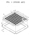
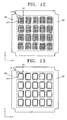
- an evaporation mask 10 used to deposit an organic film or electrodes when fabricating an organic EL device is typically supported by a frame 20, so that the evaporation mask 10 is drawn taut.
- a plurality of mask units 12, allowing a single organic EL device to be formed thereon, are formed on a single metal thin plate 11.
- the evaporation mask 10 is thinly formed and minutely patterned, if it is used without any treatment, some parts of it may droop, preventing accurate patterning. Accordingly, as shown in FIG. 1 , optimal tension in the x- and y-axis directions is applied to the evaporation mask 10 to obtain a predetermined accuracy of a total pitch (Pt), and the taut evaporation mask 10 is coupled to the mask frame 20. Upon coupling, it is important to not change the Pt accuracy.
- the coupling of the evaporation mask 10 to the mask frame 20 can be achieved by various methods such as using an adhesive, laser welding, or resistance welding.
- Each of the mask units 12 includes a pattern of apertures. As shown in FIG. 1 , each of the mask units 12 may have strip-like apertures elongated in the y-axis direction. However, the tension makes it difficult for the outermost apertures of each of the mask units 12 to maintain a predetermined level of accuracy.
- FIG. 2 is a cross-section of a mask unit 12 taken along line I-I of FIG. 1 , which shows apertures 13 formed in the mask unit 12. As shown in FIG. 2 , a shielding portion 14 is provided between adjacent apertures 13, and outermost apertures 13a are each defined by a shield portion 14 and a rib 15 between adjacent mask units.
- an edge portion 15a of the rib 15 may curve upward. Such deformation of the edge portion 15a of the rib 15 degrades the accuracy of the widths of each of the outermost apertures 13a. Hence, the accuracy of deposition performed on an organic emissive film through the outermost apertures 13a is degraded, and, consequently, accurate patterning of the organic emissive film is not accomplished outside a panel. If an edge of a rib between adjacent mask units is deformed, the deformed rib contacts the organic emissive film, thus generating a defect such as a dark point or a pixel short-circuit on the perimeter of a panel.
- this problem affects the outermost mask units more than other mask units, thus degrading the accuracy of the total mask pitch.
- mask units 12a and 12b located at the outermost sides in the direction perpendicular to the direction of the length of apertures 13, that is, in the x-axis direction where tension is applied may be deformed more seriously than other mask units 12 due to the tension applied in the x-axis direction. Accordingly, the accuracy of a total pitch (Pt), the gap between a line 16a connecting the edges of the outer ribs of the mask units 12a and a line 16b connecting the edges of the outer ribs of the mask units 12b, decreases, resulting in degradation of the accuracy of patterning of the mask units 12.
- the disclosed mask includes a mask portion and a screen portion.
- the mask portion is an evaporation mask used to form a patterning film on a substrate by evaporation, and has partitions for defining a plurality of first apertures.
- the screen portion contains a magnetic material and has a plurality of second apertures smaller than the first apertures. The second apertures are disposed on the first apertures of the mask portion.
- Japanese Patent Publication No. 2001-273979 discloses the structure of a magnetic mask.
- Japanese Patent Publication No. 2001-254169 discloses an evaporation mask frame assembly in which a patterned mask masks a deposition area while adhering closely to a material to be deposited, and has fine gaps and fine patterns. The fine patterns of the patterned mask are supported by fine ribs.
- Japanese Patent Publication No. 2002-9098 discloses a pattern forming apparatus for preventing a pre-formed film on a substrate from being damaged due to a mask coming partially off of a frame due to a thermal expansion during evaporation.
- the pattern forming apparatus includes a support which is formed to be larger than the mask, and has a dent portion onto which the mask is seated: The support prevents a mask from becoming rippled due to thermal expansion during the formation of a film. Also, by forming a magnetic element on the side of the mask facing away from the support, the magnetic element makes the mask closer to the substrate so that a space between the mask and the support is created. This space contributes to cooling the mask.
- the disclosed mask having slits is not firmly supported by the frame, the location of the mask cannot be accurately controlled.
- the location of the evaporation mask may be changed during evaporation.
- Japanese Patent Publication No. 2002-8859 discloses a pattern forming apparatus for preventing a mask from being expanded by heat during the formation of a film, in which a liquid path is formed within a frame which supports the mask, and a cooling solution circulates within the liquid path.
- this invention also overlooks the possibility of tensions and apertures becoming inaccurate during fixation of the mask into the frame.
- Japanese Patent Publication Nos. 2000-48954 , 2000-173769 , 2001-203079 , and 2001-110567 disclose metal masks including supplementary lines to prevent drooping of a mask shield between the mask and a frame. Like the above-disclosed masks, these masks may be stretched and warped while being fixed onto a frame after applying tension in order to accomplish highly accurate patterning.
- a mask structure is described in Yamazaki et al, "Slit Structure as a Countermeasure for the Thermal Deformation of a Metal Mask", Japanese Journal of Applied Physics, Volume 40 (2001) pages 7170 to 7173 .
- the mask structure includes a slit to absorb the thermal expansion of beams within the frame.
- an evaporation mask formed of a thin film according to claim 1.
- the main apertures may form an effective deposition area, and the first dummy apertures may form an ineffective deposition area.
- At least one of the first dummy apertures may be formed parallel to the main apertures, and at least another one of the first dummy apertures may be formed perpendicular to the main apertures.
- the second dummy apertures may be formed outside the effective deposition areas where the mask units are formed.
- At least one of the second dummy apertures may be formed parallel to the main apertures of the mask units, and at least another one of the second dummy apertures may be formed perpendicular to the main apertures.
- an organic electroluminescent (EL) device according to claim 5.
- At least one of the first dummy apertures may be formed parallel to the main apertures, and at least another one of the first dummy apertures may be formed perpendicular to the main apertures.
- At least two organic EL devices may be manufactured in a single process, and the evaporation mask may comprise at least two mask units, through each of which the organic film of a single organic EL device can be deposited, and a plurality of second dummy apertures outside and adjacent to outermost ones of the mask units in the direction in which tension is applied to the evaporation mask.
- the second dummy apertures of the evaporation mask may be located outside the effective luminescent areas of the organic EL devices that may be deposited by the outermost mask units adjacent to the second dummy apertures.
- At least one of the second dummy apertures may be formed parallel to the main apertures of the mask units, and at least one of the second dummy apertures may be formed perpendicular to the main apertures.
- an evaporation mask to form the second electrodes may be disposed over the substrate.
- the evaporation mask is drawn taut by application of tension and has at least one mask unit.
- the mask unit comprises a plurality of main apertures and a plurality of first dummy apertures formed adjacent to the outermost main apertures in the direction in which tension is applied to the evaporation mask.
- the second electrodes may be formed on the effective luminescent area through the main apertures, and a second dummy pattern area may be formed outside the effective luminescent area through the first dummy apertures.
- At least one of the first dummy apertures may be formed parallel to the main apertures, and at least another one of the first dummy apertures may be formed perpendicular to the main apertures.
- At least two organic EL devices may be manufactured in a single process.
- the evaporation mask may comprise at least two mask units, through each of which the second electrodes of a single organic EL device can be deposited, and a plurality of second dummy apertures outside and adjacent to the outermost mask units in the direction in which tension is applied to the evaporation mask.
- the second dummy apertures may be located outside the effective luminescent areas of the organic EL devices that are deposited by the outermost mask units adjacent to the second dummy apertures.
- At least one of the second dummy apertures may be formed parallel to the main apertures of the mask units, and at least another one of the second dummy apertures may be formed perpendicular to the main apertures.
- At least two organic EL devices may be manufactured in a single process.
- the second electrodes may be formed using an evaporation mask drawn taut by application of tension and having at least two mask units, through which the second electrodes of the organic EL device can be deposited.
- the evaporation mask may comprise a plurality of second dummy aperture outside and adjacent to outermost mask units in the direction in which tension is applied to the evaporation mask.
- the second dummy apertures may be located outside the effective luminescent areas of the organic EL devices that are deposited by the outermost mask units adjacent to the second dummy apertures.
- At least one of the second dummy apertures may be formed parallel to the main apertures of the mask units, and at least another one of the second dummy apertures may be formed perpendicular to the main apertures.
- an evaporation mask to form the second electrodes may be disposed over the substrate.
- the evaporation mask may be drawn taut by application of tension and includes at least two mask units.
- Each of the mask units may comprise a plurality of main apertures and a plurality of first dummy apertures formed adjacent to the outermost main apertures in the direction in which tension is applied to the evaporation mask.
- the second electrodes may be formed on each of the effective luminescent areas through the main apertures, and a second dummy pattern area may be formed outside each of the effective luminescent areas through the first dummy apertures.
- At least one of the first dummy apertures may be formed parallel to the main apertures, and at least another one of the first dummy apertures may be formed perpendicular to the main apertures.
- the evaporation mask may comprise a plurality of second dummy apertures outside and adjacent to the outermost mask units in the direction in which tension is applied to the evaporation mask.
- the second dummy apertures of the evaporation mask may be located outside the effective luminescent areas of the organic EL devices that are deposited by the outermost mask units adjacent to the second dummy apertures.
- At least one of the second dummy apertures may be formed parallel to the main apertures of the mask units, and at least another one of the second dummy apertures may be formed perpendicular to the main apertures.
- an organic EL device according to claim 15.
- the dummy pattern area may be formed inside an area sealed by the sealing unit.
- the dummy pattern area may be formed of the same material as the organic luminescent layer.
- the dummy pattern area may be formed of the same material as the organic film.
- the dummy pattern area may be formed of the same material as the second electrodes.
- the dummy pattern area may be formed on the outside of the organic luminescent area in an upper area of the organic film.
- the present invention provides an evaporation mask that reduces deviation of patterns by reducing variation in the accuracy of the widths of apertures that may be caused by supporting a taut evaporation mask, a method of manufacturing an organic EL device using the evaporation mask, and an organic EL device manufactured by the method.
- the present invention also provides an evaporation mask that improves pattern accuracy by compensating for a total pitch when tension is applied to the evaporation mask, a method of manufacturing an organic EL device using the evaporation mask, and an organic EL device manufactured by the method.
- an evaporation mask 20 includes a plurality of mask units 21. As shown in FIG. 4 , the plurality of mask units 21 can be patterned on many products in a single process.
- the evaporation mask 20 may be a magnetic thin plate made of nickel or an alloy of nickel and cobalt.
- the evaporation mask 20 is made of a nickel-cobalt alloy, which facilitates the formation of fine patterns and provides an excellent surface roughness. Apertures 211 and 213 in the evaporation mask 20 may be formed in a predetermined pattern by an electro-forming method so as to obtain a fine pattern and an excellent surface smoothness.
- the alloy of Ni and Co may be composed of 85% by weight nickel and 15% by weight cobalt.
- the evaporation mask 20 may be manufactured by an etching method, that is, by forming a photoresist layer having a pattern of apertures 211 and 213 on a thin plate, or attaching a film having the pattern of apertures 211 and 213 to a thin plate and then etching the resulting plate.
- tension is applied to the evaporation mask 20 manufactured by the etching method in x- and y-axis directions while its edges are fixed by a clamp or an adhesive agent. Then, the taut evaporation mask 20 is joined to a mask frame 30.
- the mask frame 30 is hollow so as to support the edge of the evaporation mask 20 excluding the portion where the mask units 21 have been formed.
- the joining can be achieved by various methods, such as using an adhesive agent, a laser welding method, or a resistance heating welding method. Especially, the laser welding method can be used to overcome a problem such as an accuracy change or the like.
- reference numeral 31 denotes a welding dot used in laser welding.
- a portion of the evaporation mask 20 to be welded to the mask frame 30 may be covered by a cover frame to prevent the evaporation mask 20 from coming off the mask frame 30, in order to overcome stretching or warping of the evaporation mask due to poor welding of the evaporation mask 20 to the mask frame 30.
- each of the mask units 21 included in the evaporation mask 20 includes a pattern of a plurality of apertures 211 and 213, which are defined by strip-like shielding portions 212.
- the apertures 211 and 213 shown in FIGS. 4 and 5 are elongated in parallel straight lines. However, the apertures 211 and 213 are not limited to such strip shapes, and can be formed in various shapes and patterns, such as lattice or mosaic shapes.
- a rib 22 is installed between adjacent mask units 21 so as to keep a distance therebetween.
- the rib 22 can be a first rib 221 for isolating mask units 21 arranged in the x-axis direction, or a second rib 222 for isolating mask units 21 arranged in the y-axis direction.
- the apertures 213 are first dummy apertures located at the outermost place in a direction in which tension is applied to the evaporation mask 20, while the apertures 211 are main apertures located inside the first dummy apertures 213.
- the first dummy apertures 213 are used to prevent apertures around the edge of each of the mask units from being deformed by tension applied to the evaporation mask 20.
- the main apertures 211 are formed in strips elongated in the y-axis direction, apertures around the edge of each of the mask units 21 may be deformed by the tension applied in the x-axis direction rather than by the tension applied in the y-axis direction.
- the first dummy apertures 213 are installed adjacent to some of the main apertures 211 located at the outer side in the x-axis direction.
- the main apertures 211 are used to form an effective deposition area that allows a deposition to form a pattern desired by a user, while the first dummy apertures 213 are used to form an ineffective deposition area.
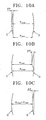
- FIG. 6 is a cross-section taken along line II-II of FIG 5 .
- First through third shielding portions 212a through 212c are sequentially formed in the x-axis direction starting from a first rib 221 to form a mask unit 21.
- First and second main apertures 211 a any 211b are sequentially formed in the x-axis direction between the first and second shielding portions 212a and 212b and between the second and third shielding portions 212b and 212c, respectively.
- a first dummy aperture 213 is formed between the first rib 221 and the first shielding portion 212a.
- the width Ws1 of the first main aperture 211a has a deviation of ⁇ Ws1
- the width Ws2 of the second main aperture 211b has a deviation of ⁇ Ws2.
- ⁇ Wr1 denotes a deviation of the width Wr1 of the first shielding portion 212a
- ⁇ Wsd denotes a deviation of the width Wsd of the first dummy aperture 213.
- FIG. 7 when tension is applied to the evaporation mask having the apertures with the above widths, an edge 221a of the first rib 221 that defines the first dummy aperture 213 located at the edge area of the mask unit 21 is lifted upward or downward due to the extension of the evaporation mask in the x-axis direction shown in FIGS. 4 and 5 . Hence, the deviation ⁇ Wsd of the width Wsd of the first dummy aperture 213 increases.
- FIG. 8 The deviation of the apertures of the evaporation mask after application of tension is shown in FIG. 8 .
- reference character A refers to an evaporation mask manufactured by electroforming
- reference character B refers to an evaporation mask manufactured by etching.
- the deviation of the width of each of the main apertures typically depends on the deviations of the widths of the shielding portions, ⁇ Wr1, ⁇ Wr2, ⁇ Wr3, ...
- the deviations of the widths of the first dummy aperture 213 and the first and second main apertures 211a and 211b, ⁇ Wsd, ⁇ Ws1 , and ⁇ Ws2, shown in FIG. 8 are divided by the deviation ⁇ Wr1 of the width of the first shielding portion and then expressed as percentage.
- the deviation ⁇ Wsd of the width of the first dummy aperture 213 increases by 25 to 75% of the deviation ⁇ Wr1 of the width of the first shielding portion due to deformation of the edge 221 a of the first rib 221.
- the deviations of the widths of the first and second main apertures 211a and 211b, ⁇ Ws1 and ⁇ Ws2, are nearly the same as the deviation ⁇ Wr1 of the width of the first shielding portion.
- the total pitch Pt is determined as the interval between lines C and D which connect the outermost first main apertures 211 a of two mask units 21 a in the x-axis direction.
- the total pitch Pt may have a deviation (Pt max - Pt min).
- a line deviation ( ⁇ X) may be generated.
- the first dummy apertures 213 may have the same shape and width as the main apertures 211, and may be spaced apart from an adjacent first main aperture 211 a by the same interval as the interval between adjacent main apertures 211.
- the first dummy apertures 213 are not limited to the above shape and pattern; any shape and pattern may be adopted as long as the pattern of the main apertures 211 is not affected. For example, as shown in FIG.
- the width Wsd of a first dummy aperture 213 may be smaller than the width Ws1 of a first main aperture 211 a, and the width Wr1 of the first shielding portion 212a between the first dummy aperture 213 and the first main aperture 211 a may be greater than the width Wr2 of the second shielding portion 212b between the first and second main apertures 211 a and 211 b.
- various shapes and patterns may be applied.
- first dummy apertures 213 are formed near the main apertures located at the outermost edges of each of the mask units 21.
- the first dummy apertures 213 may have a length corresponding to the length of one side of a mask unit 21 and be formed at each side of each mask unit.
- a plurality of first dummy apertures having a length corresponding to the length of one side of each of the lattice-like main apertures 211 may be arranged at each side of each mask unit.
- the installation of the first dummy apertures 213 of FIG. 12 can also be applied to an evaporation mask 20 of FIG. 13 , which includes open mask units 21 that each have a single main aperture 211.
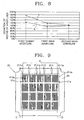
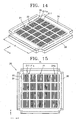
- an evaporation mask 20 according to another comparative example of the present invention includes second dummy apertures 22 to improve accuracy.
- FIG. 15 is a plan view of the evaporation mask 20 of FIG. 14 .
- the evaporation mask 20 includes at least two mask units 21 having a predetermined pattern of main apertures 211. At least one second dummy aperture 22 is formed outside the mask units 21 such as to be adjacent to mask units 21a and 21b located at the outermost edges in the direction where tension is applied.
- the main apertures 211 of the evaporation mask 20 are strips elongated in the y-axis direction, they are seriously deformed in the x-axis direction, and accordingly, the total pitch Pt is distorted in the x-axis direction.
- the distortion of the total pitch Pt is prevented by forming the second dummy apertures 22 so as to be adjacent to columns of masks 21 a and masks 21 b that are located on the edges of the evaporation mask 20, particularly, at the outermost sides in the x-axis direction.
- the main apertures 211 formed inside the second dummy apertures 22 are prevented from being deformed due to the tension. Consequently, the total pitch Pt is compensated.
- the second dummy apertures 22 can be formed in the same shape and with the same width as the main apertures 211.
- the second dummy apertures 22 can have various shapes and patterns as long as they don't affect the pattern of the main apertures 211.
- the second dummy apertures 22 may be formed on the exterior sides of the outermost mask units 21 a and 21 b so as to be as close as possible to the outermost mask units 21 a and 21 b without interfering with deposition areas desired by a user, that is, with effective deposition areas where deposition is achieved through the outermost mask units 21 a and 21b.
- the second dummy apertures 22 must be located inside the welding dots 31 of the evaporation mask 20.
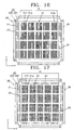
- alignment marks 23 are formed outside a configuration of mask units 21 in order to assist in alignment with a substrate where deposition is to be performed, the alignment marks 23 must not be deformed when tension is applied to the evaporation mask 20. If the alignment marks 23 are deformed, the evaporation mask 20 is not properly aligned with the substrate, thus causing distortion of the total pitch and inaccurate patterning.
- a pair of second dummy apertures 221 and 222 is formed at both sides of each of the alignment marks 23.
- the inner second dummy aperture 221 prevents the total pitch Pt from being distorted, thereby increasing the accuracy of patterning.
- the outer second dummy aperture 222 prevents the alignment marks 23 from being deformed, thereby accurately aligning the substrate with the evaporation mask 20.
- the second dummy apertures 22 can be equally applied to the case where the main apertures 211 of each of the mask units 21 are formed in a lattice pattern.
- the main apertures 211 have a lattice pattern, a tension in the y-axis direction as well as a tension in the x-axis direction adversely affects the accuracy of the total pitch Pt, so second dummy apertures 22 are also formed adjacent to the main apertures located at the outermost sides in the y-axis direction.
- the way of installing the second dummy apertures 22 as in FIG. 17 is also applied to an evaporation mask 20 of FIG. 18 including open mask units 21, each formed of a single main aperture 211.
- the total pitch corresponds to the interval between the outermost main apertures in the outermost mask units.
- the evaporation mask 20 according to the present invention is not limited to the above determination of the length of the total pitch, but can be formed of a combination of the first dummy apertures 213 and the second dummy apertures 22 as shown in FIG. 19 .
- the combination of the first and second dummy apertures 213 and 22, respectively may be a combination of all of the above-described examples.
- each of the mask units 21 prevents deformation of its main apertures forming an effective deposition area and improves the accuracy of the total pitch. Thus, highly accurate patterning can be achieved.
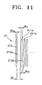
- a transparent conductive film 43 and a metal conductive film 44 are sequentially stacked on a transparent substrate 41.
- the transparent conductive film 43 may be formed of ITO, and the metal conductive film 44 may be formed of chrome (Cr).
- the substrate 41 may be formed of transparent glass, plastic, or the like.
- a buffer layer 42 may be formed to provide a smooth substrate and prevent penetration of impure atoms.
- the buffer layer 42 may be formed of SiO 2 .
- the substrate 41 may be large enough to form at least two organic EL devices thereon through a single process.
- FIG. 21 refers to the case where a plurality of organic EL devices are manufactured in a single process. However, for convenience of explanation, the manufacture of a single organic EL device will now be described by cutting off an organic EL device from the plurality of EL devices as shown in FIG. 21 .
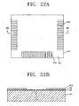
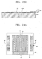
- FIG. 22A refers to an organic EL device of FIG. 21
- FIG. 22B is a cross-section taken along line III-III of FIG. 22A
- the external electrode terminals 441 and 442 are the basis of the formation of the first and second electrode terminals 51 and 52 of FIG 23A
- the transparent conductive film 43 is partially exposed on the substrate 41.
- FIGS. 23A through 23C internal electrode terminals 431 and 432 for the first and second electrodes 51 and 52 and a predetermined pattern of transparent conductive lines 433 are formed by patterning the exposed portion of the transparent conductive film 43 on the substrate 41.
- the transparent conductive lines 433 are connected to the first electrode terminals 51 and serve as first electrode lines 61.
- FIG. 23B is a cross-section taken along line IV-IV of FIG. 23A
- FIG. 23C is a cross-section taken along line V-V of FIG. 23A .
- the patterning of the transparent conductive film 43 may be achieved by photolithography.
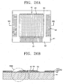
- FIG. 24B is a cross-section taken along line VI-VI of FIG. 24A .
- the inter-insulator 64 may be formed of photoresist, photosensitive polyimide, or the like using a photolithography method or the like.
- a shielding wall may be further formed inside and outside a place to be coated with an adhesive agent so as to seal up a cap, and an outer-insulator may be formed between the first electrode line 61 and the second electrode terminal 52.
- the outer-insulator is formed to prevent problems such as disconnection due to the step difference between second electrode lines and the second electrode terminals 52 upon formation of the second electrode lines.
- a buffer layer may be further formed below the outer-insulator by processing the transparent conductive film 43 to improve the adhesive strength between the outer- insulator and a substrate.
- Separators may be simultaneously formed to form an organic EL film and a pattern of second electrode lines. Partitions for preventing the organic EL film from being damaged may be formed simultaneously. Shielding portions may be formed simultaneously on the place to be coated with an adhesive agent.
- an organic film is deposited using an evaporation apparatus shown in FIG. 25 .
- an evaporation source 92 for evaporating an organic material is installed within a chamber 91 in a vacuum state, and the evaporation mask 20 supported by the mask frame 30 is installed over the evaporation source 92.
- the substrate 41 having first electrode lines and an inter-insulator formed thereon is mounted over the evaporation mask 20.
- a magnet unit 93 is closely installed over the substrate 41.
- an organic film 63 is deposited using an evaporation apparatus as shown in FIG. 25 .
- the organic film 63 can be any organic film used in an organic EL device, and can be formed by stacking a hole transport layer, an organic luminescent layer, an electron transport layer, and the like to form a single or complex structure.
- the organic film 63 can be made of various organic materials including copper phthalocyanine (CuPc), N, N'-Di (naphthalene-1-yl)-N, N'-diphenylbenzidine (NPB), and tris-8-hydroxyquinoline aluminum (Alq3).
- CuPc copper phthalocyanine
- NPB N'-Di (naphthalene-1-yl)-N
- NPB N'-diphenylbenzidine
- Alq3 tris-8-hydroxyquinoline aluminum
- the organic film 63 can be formed in various patterns such that the patterned organic luminescent layer corresponds to the color of each pixel.
- the organic film 63 may be formed after the evaporation mask 20 is mounted on the evaporation apparatus of FIG. 25 .
- the evaporation mask 20 may be the evaporation mask 20 according to any of the embodiments of the present invention described with reference to FIGS. 4 through 19 .
- the evaporation mask 20 having the main apertures 211 and the first dummy apertures 213 can be used to form an organic film.
- the first dummy apertures 213 are formed adjacent to the outermost main apertures 211 a in a direction in which tension is applied, i.e., in a direction perpendicular to the direction of the length of the main apertures 211.
- the evaporation mask 20 having the second dummy apertures 22, included in at least two mask units for forming an organic EL device can be used to form an organic film.
- the second dummy apertures 22 are formed outside the mask units, adjacent to mask units in a direction in which tension is applied, i.e., in a direction perpendicular to the direction of the length of the main apertures 211. Furthermore, although not shown in the drawings, an evaporation mask having both the first and second dummy apertures 213 and 22, respectively, can be used to form an organic film.
- FIG. 26C is a partially magnified cross-section of the portion indicated by reference character VIII.
- the organic film 63 is formed by depositing a hole transport layer 631 on the first electrode lines 61 and the inter-insulators 64 and then depositing red (R), green (G), and blue (B) organic luminescent layers 632 on the hole transport layer 631 such as to form color patterns.
- the hole transport layer 631 can be blanket deposited without patterns, and the organic luminescent layers 632 may be formed in a pattern.
- the organic luminescent layers 632 having a pattern are deposited using the above-described evaporation masks according to the present invention.
- the R, G, and B organic luminescent layers 632 formed on the first electrode lines 61, correspond to areas where the first electrode lines intersect with the second electrode lines, and accordingly emit light in response to the application of power.
- the R, G, and B organic luminescent layers 632 form an effective luminescent area 60.
- dummy organic luminescent layers 632a are further deposited between the second electrode terminals 52 and the first electrode lines 61, that is, the effective luminescent area 60, through the first dummy apertures.
- the dummy organic luminescent layers 632a form the first dummy pattern area 70.
- the first dummy pattern area 70 further includes a dummy hole transport layer 631a.
- organic films can be deposited to the same height in the first dummy pattern area 70 by controlling the widths of the first dummy apertures 213 of FIG. 13 .
- the variation of the total pitch is reduced to thus improve the accuracy of patterning of the effective luminescent area, particularly the organic luminescent layers.
- the first dummy pattern area 70 Since the first dummy pattern area 70 is formed outside the effective luminescent area 60 where the first electrode lines intersect with the second electrode lines, that is, formed in an area where the first electrode lines do not intersect with the second electrode lines, the first dummy pattern area 70 corresponds to an ineffective luminescent area where no light emission occurs.
- the deposition using an evaporation mask capable of forming the first dummy pattern area 70 contributes to improvement of the accuracy of patterning in the effective luminescent area 60.
- the second electrode lines 62 may be formed of aluminum (AI) or calcium (Ca) in a predetermined pattern on the organic film 63 such as to intersect with the first electrode lines 61.
- the second electrode lines 62 may be formed using an evaporation mask in an evaporation apparatus as shown in FIG. 25 .
- the second electrode lines 62 may be patterned using an evaporation mask having a predetermined pattern or by previously installing a separator for forming a pattern and then performing blanket deposition on the separator.
- the second electrode lines 62 can be patterned using the evaporation mask having first and/or second dummy apertures described with reference to FIGS. 4 through 19 .
- FIG. 29 shows an example of patterning the second electrode lines 62 using an evaporation mask.
- the evaporation mask 20 of FIG. 4 having a pattern of main apertures 211 and the first dummy apertures 213, is used to form the second electrode lines 62, second dummy electrode lines 62a are deposited on the exterior side of the effective luminescent area 60, which is where the organic film 63 emits light due to the crossing of the first and second electrode lines 61 and 62.
- the second dummy electrode lines 62a form a second dummy pattern area 71. Because the second dummy electrode lines 62a are not connected to second electrode terminals which receive external power, the second dummy pattern area 71 corresponds to an ineffective luminescent area where no light emission occurs, as in the first dummy pattern area 70. As shown in FIG. 29 , preferably, the second dummy electrode lines 62a may be formed outside the effective luminescent area 60 on the upper surface of the organic film 63 so as not to contact the first electrode lines 61.
- a method of depositing an organic film using an evaporation mask forming an organic film and depositing second electrode lines using an evaporation mask forming second electrodes is described above. However, it is natural that the second electrode lines may be deposited using an evaporation mask according to the present invention regardless of which evaporation mask is used to deposit the organic film.
- a sealing cap 81 is joined to the substrate 41 so as to serve as a sealing portion 80.
- a flexible printed circuit board 82 is connected to the first and second electrode terminals 51 and 52 exposed to the outside of the sealing portion 80, thereby completing the assembly of an organic EL device.
- the sealing may be achieved by any other methods applied to organic EL devices.
- the organic EL device according to the present invention has the effective luminescent area 60 where an organic film is formed between the first and second electrode lines 61 and 62.
- the organic EL device according to the present invention also includes a terminal unit 50 having the first and second electrode terminals 51 and 52, which supply power to the first and second electrode lines 61 and 62, respectively, of the effective luminescent area 60.
- the organic EL device according to the present invention may include the second dummy pattern area 71 and/or the first dummy pattern area 70, which is formed outside the effective luminescent area 60, that is, between the effective luminescent area 60 and the terminal unit 50. Since the structures and functions of the components of the organic EL device according to the present invention have been described with reference to FIGS. 20 through 29 , they will not be described here in detail.
- an organic EL device having first and second dummy pattern areas in an ineffective luminescent area is manufactured using an evaporation mask having first and second dummy apertures, thereby improving the accuracy of patterning of an effective luminescent area where light emission occurs.
- the present invention has the following effects. Firstly, the accuracy of the patterning of an effective deposition area may be improved.
- the accuracy of the total pitch is improved, and thus the manufacturing yield may be improved.
- a substrate may be accurately aligned with an evaporation mask.
- an organic EL device includes a dummy pattern area, that is, an ineffective luminescent area, an effective luminescent area where light emission occurs may have smaller pixels, resulting in a finer resolution.
Landscapes
- Chemical & Material Sciences (AREA)
- Engineering & Computer Science (AREA)
- Chemical Kinetics & Catalysis (AREA)
- Materials Engineering (AREA)
- Mechanical Engineering (AREA)
- Metallurgy (AREA)
- Organic Chemistry (AREA)
- Manufacturing & Machinery (AREA)
- Electroluminescent Light Sources (AREA)
- Physical Vapour Deposition (AREA)
Applications Claiming Priority (2)
| Application Number | Priority Date | Filing Date | Title |
|---|---|---|---|
| JP2002347977A JP4173722B2 (ja) | 2002-11-29 | 2002-11-29 | 蒸着マスク、これを利用した有機el素子の製造方法及び有機el素子 |
| JP2002347977 | 2002-11-29 |
Publications (2)
| Publication Number | Publication Date |
|---|---|
| EP1426461A1 EP1426461A1 (en) | 2004-06-09 |
| EP1426461B1 true EP1426461B1 (en) | 2011-03-16 |
Family
ID=32310666
Family Applications (1)
| Application Number | Title | Priority Date | Filing Date |
|---|---|---|---|
| EP03257499A Expired - Lifetime EP1426461B1 (en) | 2002-11-29 | 2003-11-27 | Mask for coating by vacuum evaporation |
Country Status (6)
| Country | Link |
|---|---|
| US (2) | US7837528B2 (zh) |
| EP (1) | EP1426461B1 (zh) |
| JP (1) | JP4173722B2 (zh) |
| KR (1) | KR100922753B1 (zh) |
| CN (2) | CN100492715C (zh) |
| DE (1) | DE60336371D1 (zh) |
Cited By (1)
| Publication number | Priority date | Publication date | Assignee | Title |
|---|---|---|---|---|
| EP3569730B1 (en) * | 2017-01-10 | 2024-05-08 | Dai Nippon Printing Co., Ltd. | Vapor deposition mask, method for manufacturing vapor deposition mask device, and method for manufacturing vapor deposition mask |
Families Citing this family (109)
| Publication number | Priority date | Publication date | Assignee | Title |
|---|---|---|---|---|
| CN100464440C (zh) * | 2002-06-03 | 2009-02-25 | 三星移动显示器株式会社 | 用于有机电致发光装置的薄层真空蒸发的掩模框组件 |
| JP4173722B2 (ja) | 2002-11-29 | 2008-10-29 | 三星エスディアイ株式会社 | 蒸着マスク、これを利用した有機el素子の製造方法及び有機el素子 |
| JP4506214B2 (ja) * | 2003-03-13 | 2010-07-21 | 東レ株式会社 | 有機電界発光装置およびその製造方法 |
| JP4230258B2 (ja) * | 2003-03-19 | 2009-02-25 | 東北パイオニア株式会社 | 有機elパネル、有機elパネルの製造方法 |
| JP4463492B2 (ja) * | 2003-04-10 | 2010-05-19 | 株式会社半導体エネルギー研究所 | 製造装置 |
| KR100889764B1 (ko) * | 2003-10-04 | 2009-03-20 | 삼성모바일디스플레이주식회사 | 유기 전자 발광 소자의 박막 증착용 마스크 프레임 조립체및, 그것을 이용한 박막 증착 방법 |
| JP4608874B2 (ja) * | 2003-12-02 | 2011-01-12 | ソニー株式会社 | 蒸着マスクおよびその製造方法 |
| JP4944367B2 (ja) * | 2004-05-25 | 2012-05-30 | キヤノン株式会社 | マスク構造体の製造方法 |
| KR100627110B1 (ko) * | 2004-06-01 | 2006-09-25 | 엘지전자 주식회사 | 마스크 장치와 이를 이용한 유기전계발광표시소자의제조방법 |
| JP4538650B2 (ja) * | 2004-06-18 | 2010-09-08 | 京セラ株式会社 | 蒸着装置 |
| KR100659057B1 (ko) * | 2004-07-15 | 2006-12-21 | 삼성에스디아이 주식회사 | 박막 증착용 마스크 프레임 조립체 및 유기 전계 발광표시장치 |
| JP4656886B2 (ja) * | 2004-07-23 | 2011-03-23 | 大日本印刷株式会社 | 金属薄板の枠貼り方法及び装置 |
| JP4671680B2 (ja) * | 2004-12-16 | 2011-04-20 | 大日本印刷株式会社 | メタルマスクのフレーム取付方法及び装置 |
| KR100972182B1 (ko) | 2004-07-23 | 2010-07-26 | 다이니폰 인사츠 가부시키가이샤 | 금속 박판을 프레임에 부착하는 방법 및 장치 |
| US7531216B2 (en) * | 2004-07-28 | 2009-05-12 | Advantech Global, Ltd | Two-layer shadow mask with small dimension apertures and method of making and using same |
| KR101070539B1 (ko) | 2004-09-08 | 2011-10-05 | 도레이 카부시키가이샤 | 증착 마스크 및 이를 사용한 유기 전계 발광 장치의 제조 방법 |
| WO2006027830A1 (ja) * | 2004-09-08 | 2006-03-16 | Toray Industries, Inc. | 有機電界発光装置およびその製造方法 |
| JP4606114B2 (ja) * | 2004-10-15 | 2011-01-05 | 大日本印刷株式会社 | メタルマスク位置アラインメント方法及び装置 |
| US20060081184A1 (en) * | 2004-10-19 | 2006-04-20 | Yeh Te L | Evaporation mask with high precision deposition pattern |
| KR101102022B1 (ko) | 2004-10-26 | 2012-01-04 | 엘지디스플레이 주식회사 | 마스크 장치와 이를 이용한 유기전계발광표시소자의제조방법 |
| KR100603398B1 (ko) | 2004-11-18 | 2006-07-20 | 삼성에스디아이 주식회사 | 증착용 마스크 및 전계발광 디스플레이 장치 |
| KR100626041B1 (ko) * | 2004-11-25 | 2006-09-20 | 삼성에스디아이 주식회사 | 평판표시장치의 박막 증착용 마스크 및 그의 제조방법 |
| KR100676175B1 (ko) * | 2005-03-18 | 2007-02-01 | 엘지전자 주식회사 | 유기 전계 발광 소자 제조용 마스크 |
| KR20070015328A (ko) * | 2005-07-30 | 2007-02-02 | 삼성에스디아이 주식회사 | 평판 디스플레이 장치 |
| US8401675B2 (en) * | 2005-12-16 | 2013-03-19 | Intellischematic, Llc | Methods and systems for machine-related information delivery |
| US20090151630A1 (en) * | 2006-05-10 | 2009-06-18 | Advantech Global, Ltd. | Tensioned aperture mask and method of mounting |
| KR101241140B1 (ko) | 2006-06-26 | 2013-03-08 | 엘지디스플레이 주식회사 | 섀도우마스크와 이를 이용한 유기전계발광소자 및 그제조방법 |
| KR100814818B1 (ko) * | 2006-07-31 | 2008-03-20 | 삼성에스디아이 주식회사 | 유기 발광 표시 장치 제조용 마스크 |
| US8198624B2 (en) * | 2006-08-03 | 2012-06-12 | Lg Display Co., Ltd. | Organic light emitting device |
| KR100836471B1 (ko) * | 2006-10-27 | 2008-06-09 | 삼성에스디아이 주식회사 | 마스크 및 이를 이용한 증착 장치 |
| KR100880944B1 (ko) * | 2007-10-01 | 2009-02-04 | 엘지디스플레이 주식회사 | 유기발광표시장치 |
| KR100908658B1 (ko) | 2007-11-20 | 2009-07-21 | 엘지디스플레이 주식회사 | 유기발광표시장치 |
| KR100947442B1 (ko) * | 2007-11-20 | 2010-03-12 | 삼성모바일디스플레이주식회사 | 수직 증착형 마스크 제조장치 및 이를 이용한 수직 증착형마스크의 제조방법 |
| KR101450728B1 (ko) * | 2008-05-28 | 2014-10-14 | 삼성디스플레이 주식회사 | 마스크 조립체 및 그의 제조 방법 |
| KR20100026655A (ko) | 2008-09-01 | 2010-03-10 | 삼성모바일디스플레이주식회사 | 박막 증착용 마스크 및 이를 이용한 유기전계발광 소자의 제조방법 |
| KR101097305B1 (ko) * | 2009-03-09 | 2011-12-23 | 삼성모바일디스플레이주식회사 | 더미 슬릿부를 차단하는 차단부를 구비한 고정세 증착 마스크, 상기 고정세 증착 마스크를 이용한 유기 발광 소자의 제조 방법, 및 상기 제조 방법에 의해 제조된 유기 발광 소자 |
| KR101156432B1 (ko) * | 2009-12-15 | 2012-06-18 | 삼성모바일디스플레이주식회사 | 박막 증착용 마스크 프레임 조립체 및 유기 발광 디스플레이 장치 |
| KR101182440B1 (ko) * | 2010-01-11 | 2012-09-12 | 삼성디스플레이 주식회사 | 박막 증착용 마스크 프레임 조립체 |
| KR101182239B1 (ko) | 2010-03-17 | 2012-09-12 | 삼성디스플레이 주식회사 | 마스크 및 이를 포함하는 마스크 조립체 |
| KR101156442B1 (ko) * | 2010-04-29 | 2012-06-18 | 삼성모바일디스플레이주식회사 | 마스크 프레임 조립체 |
| JP2011256409A (ja) * | 2010-06-04 | 2011-12-22 | Sk Link:Kk | 支持体付きメタルマスク装置及びそれを用いた装置の製造方法 |
| JP2012064564A (ja) | 2010-08-17 | 2012-03-29 | Canon Inc | 成膜マスク及び有機el表示装置の製造方法 |
| JP2012059631A (ja) * | 2010-09-10 | 2012-03-22 | Hitachi Displays Ltd | 有機エレクトロルミネッセンス用マスク |
| KR101693578B1 (ko) * | 2011-03-24 | 2017-01-10 | 삼성디스플레이 주식회사 | 증착 마스크 |
| KR101820020B1 (ko) * | 2011-04-25 | 2018-01-19 | 삼성디스플레이 주식회사 | 박막 증착용 마스크 프레임 어셈블리 |
| KR101813549B1 (ko) * | 2011-05-06 | 2018-01-02 | 삼성디스플레이 주식회사 | 분할 마스크와 그 분할 마스크를 포함한 마스크 프레임 조립체의 조립장치 |
| KR20130028165A (ko) * | 2011-06-21 | 2013-03-19 | 삼성디스플레이 주식회사 | 마스크 유닛 |
| JP5770041B2 (ja) * | 2011-07-29 | 2015-08-26 | 株式会社ブイ・テクノロジー | フォトマスク及び露光装置 |
| KR101854796B1 (ko) * | 2011-09-15 | 2018-05-09 | 삼성디스플레이 주식회사 | 마스크 제조 방법 |
| KR20130057794A (ko) * | 2011-11-24 | 2013-06-03 | 삼성디스플레이 주식회사 | 증착용 마스크 및 증착용 마스크의 제조 방법 |
| KR101931770B1 (ko) * | 2011-11-30 | 2018-12-24 | 삼성디스플레이 주식회사 | 마스크 조립체 및 유기 발광 표시장치 |
| KR20130081528A (ko) * | 2012-01-09 | 2013-07-17 | 삼성디스플레이 주식회사 | 증착 마스크 및 이를 이용한 증착 설비 |
| CN103203549B (zh) * | 2012-01-16 | 2015-11-25 | 昆山允升吉光电科技有限公司 | 一种应用于掩模板组装的激光焊接方法 |
| KR101879831B1 (ko) * | 2012-03-21 | 2018-07-20 | 삼성디스플레이 주식회사 | 플렉시블 표시 장치, 유기 발광 표시 장치 및 플렉시블 표시 장치용 원장 기판 |
| KR102024853B1 (ko) * | 2012-09-03 | 2019-11-05 | 삼성디스플레이 주식회사 | 단위 마스크 및 마스크 조립체 |
| KR101980232B1 (ko) | 2012-11-14 | 2019-05-21 | 삼성디스플레이 주식회사 | 패터닝 슬릿 시트 프레임 어셈블리 |
| KR102002494B1 (ko) * | 2012-11-30 | 2019-07-23 | 삼성디스플레이 주식회사 | 박막 증착용 마스크 프레임 어셈블리 |
| CN103869601A (zh) * | 2012-12-10 | 2014-06-18 | 昆山允升吉光电科技有限公司 | 一种具有固定辅助边的掩模板及其制作方法 |
| KR102100446B1 (ko) | 2012-12-10 | 2020-04-14 | 삼성디스플레이 주식회사 | 박막 증착용 마스크 조립체 및 이의 제조 방법 |
| CN103014618A (zh) * | 2012-12-25 | 2013-04-03 | 唐军 | 蒸镀用掩模板及其制造方法 |
| CN103911583B (zh) * | 2012-12-29 | 2016-04-27 | 上海天马微电子有限公司 | Amoled金属掩膜板 |
| CN104018116A (zh) * | 2013-03-01 | 2014-09-03 | 昆山允升吉光电科技有限公司 | 一种具有辅助开口的掩模板及其制作方法 |
| CN104120380A (zh) * | 2013-04-27 | 2014-10-29 | 昆山允升吉光电科技有限公司 | 一种有机发光显示器蒸镀用掩模板及其组件 |
| KR102099238B1 (ko) * | 2013-05-13 | 2020-04-10 | 삼성디스플레이 주식회사 | 마스크 조립체 및 이를 이용한 박막 증착 방법 |
| KR102106336B1 (ko) | 2013-07-08 | 2020-06-03 | 삼성디스플레이 주식회사 | 증착용 마스크 |
| TWI480399B (zh) | 2013-07-09 | 2015-04-11 | 金屬遮罩 | |
| KR102117088B1 (ko) * | 2013-08-09 | 2020-06-01 | 삼성디스플레이 주식회사 | 유기 발광 표시 장치의 제조 장치 및 제조 방법 |
| KR20150019695A (ko) * | 2013-08-14 | 2015-02-25 | 삼성디스플레이 주식회사 | 단위 마스크 및 마스크 조립체 |
| JP2015127441A (ja) * | 2013-12-27 | 2015-07-09 | 大日本印刷株式会社 | 蒸着マスク装置の製造方法 |
| CN103882375B (zh) * | 2014-03-12 | 2016-03-09 | 京东方科技集团股份有限公司 | 一种掩膜板及其制作方法 |
| KR20160000069A (ko) * | 2014-06-23 | 2016-01-04 | 삼성디스플레이 주식회사 | 마스크 프레임 어셈블리 및 그 제조방법 |
| CN104062842B (zh) * | 2014-06-30 | 2019-02-15 | 上海天马有机发光显示技术有限公司 | 一种掩模板及其制造方法、工艺装置 |
| CN105489522B (zh) * | 2014-10-11 | 2018-10-23 | 中芯国际集成电路制造(上海)有限公司 | 光刻版及晶圆或晶圆承载台沾污的检测方法 |
| KR102250047B1 (ko) | 2014-10-31 | 2021-05-11 | 삼성디스플레이 주식회사 | 마스크 프레임 조립체, 그 제조 방법 및 유기 발광 표시 장치의 제조 방법 |
| CN104451538B (zh) * | 2014-12-30 | 2017-06-06 | 合肥鑫晟光电科技有限公司 | 掩膜板及其制作方法 |
| JP6185498B2 (ja) * | 2015-02-12 | 2017-08-23 | 株式会社半導体エネルギー研究所 | 蒸着用マスク |
| CN104651778B (zh) * | 2015-03-13 | 2016-04-27 | 京东方科技集团股份有限公司 | 一种金属掩膜板及其制作出的有机电致发光显示器件 |
| KR102352280B1 (ko) * | 2015-04-28 | 2022-01-18 | 삼성디스플레이 주식회사 | 마스크 프레임 조립체 제조 장치 및 이를 이용한 마스크 프레임 조립체 제조 방법 |
| KR102411542B1 (ko) * | 2015-05-19 | 2022-06-22 | 삼성디스플레이 주식회사 | 유기 발광 표시 장치의 픽셀 패터닝 및 픽셀 위치 검사 방법과 그 패터닝에 사용되는 마스크 |
| JP2017008342A (ja) * | 2015-06-17 | 2017-01-12 | 株式会社ブイ・テクノロジー | 成膜マスク及び成膜マスクの製造方法 |
| US10199588B2 (en) | 2015-08-18 | 2019-02-05 | Massachusetts Institute Of Technology | Planar mixed-metal perovskites for optoelectronic applications |
| JP2017071842A (ja) * | 2015-10-09 | 2017-04-13 | 株式会社ジャパンディスプレイ | 成膜用マスク及びそれを用いた成膜方法 |
| JP2017150017A (ja) * | 2016-02-23 | 2017-08-31 | 株式会社ジャパンディスプレイ | 蒸着マスクの製造方法及び有機elディスプレイの製造方法 |
| JP6954343B2 (ja) * | 2016-03-16 | 2021-10-27 | 大日本印刷株式会社 | 蒸着マスク |
| KR102696806B1 (ko) * | 2016-09-22 | 2024-08-21 | 삼성디스플레이 주식회사 | 증착용 마스크, 표시 장치의 제조 장치 및 표시 장치의 제조 방법 |
| CN107868931A (zh) | 2016-09-23 | 2018-04-03 | 昆山国显光电有限公司 | 精密金属遮罩、oled基板及其对位方法 |
| US10546537B2 (en) * | 2016-11-02 | 2020-01-28 | Innolux Corporation | Display device with display drivers arranged on edge thereof |
| US20180125182A1 (en) * | 2016-11-07 | 2018-05-10 | Cathy Barouch | Wrapped Jewelry Assembly |
| CN106583958B (zh) * | 2016-12-21 | 2019-01-15 | 信利(惠州)智能显示有限公司 | 一种掩膜版的焊接方法 |
| JP6252668B2 (ja) * | 2016-12-28 | 2017-12-27 | 大日本印刷株式会社 | 蒸着マスクの製造方法 |
| KR102333411B1 (ko) * | 2017-01-10 | 2021-12-02 | 다이니폰 인사츠 가부시키가이샤 | 증착 마스크, 증착 마스크 장치의 제조 방법 및 증착 마스크의 제조 방법 |
| JP2018170152A (ja) * | 2017-03-29 | 2018-11-01 | Tianma Japan株式会社 | Oled表示装置の製造方法、マスク及びマスクの設計方法 |
| JP7232882B2 (ja) * | 2017-03-29 | 2023-03-03 | 天馬微電子有限公司 | Oled表示装置の製造方法、マスク及びマスクの設計方法 |
| CN108977761B (zh) * | 2017-06-02 | 2020-04-03 | 京东方科技集团股份有限公司 | 掩膜板、掩膜装置及其制造方法和掩膜制造设备 |
| KR102300029B1 (ko) * | 2017-07-27 | 2021-09-09 | 삼성디스플레이 주식회사 | 마스크 프레임 조립체와 이의 제조 방법 및 표시 장치의 제조 방법 |
| KR20190014272A (ko) * | 2017-07-31 | 2019-02-12 | 삼성디스플레이 주식회사 | 표시 장치의 제조 방법 |
| CN111886356A (zh) * | 2018-03-20 | 2020-11-03 | 夏普株式会社 | 成膜用掩模及使用该成膜用掩模的显示装置的制造方法 |
| WO2019186629A1 (ja) * | 2018-03-26 | 2019-10-03 | シャープ株式会社 | 蒸着マスク、蒸着マスクセット、蒸着マスクの製造方法、蒸着マスクセットの製造方法及び表示デバイスの製造方法 |
| KR102514115B1 (ko) * | 2018-06-12 | 2023-03-28 | 삼성디스플레이 주식회사 | 증착용 마스크 및 이를 포함하는 마스크 조립체 |
| CN111384311B (zh) * | 2018-12-28 | 2023-09-08 | 乐金显示有限公司 | 用于显示器的掩模 |
| CN109778116B (zh) * | 2019-03-28 | 2021-03-02 | 京东方科技集团股份有限公司 | 一种掩膜版及其制作方法、掩膜版组件 |
| CN110246989B (zh) * | 2019-05-07 | 2021-04-30 | 信利半导体有限公司 | 一种全彩oled显示器的制作方法 |
| CN112501558A (zh) * | 2019-08-28 | 2021-03-16 | 京东方科技集团股份有限公司 | 掩膜版、掩膜装置及掩膜版的设计优化方法 |
| CN110396660B (zh) * | 2019-08-30 | 2021-10-08 | 昆山国显光电有限公司 | 掩膜板及掩膜板制备方法 |
| WO2021046807A1 (zh) * | 2019-09-12 | 2021-03-18 | 京东方科技集团股份有限公司 | 掩膜装置及其制造方法、蒸镀方法、显示装置 |
| KR20210116763A (ko) * | 2020-03-13 | 2021-09-28 | 삼성디스플레이 주식회사 | 마스크 제조방법 및 표시 장치의 제조방법 |
| KR20220022002A (ko) * | 2020-08-14 | 2022-02-23 | 삼성디스플레이 주식회사 | 금속 마스크 및 이를 이용하여 제조된 표시 장치 |
| KR20220027353A (ko) * | 2020-08-26 | 2022-03-08 | 삼성디스플레이 주식회사 | 마스크 및 마스크 제조방법 |
| US11659759B2 (en) * | 2021-01-06 | 2023-05-23 | Applied Materials, Inc. | Method of making high resolution OLED fabricated with overlapped masks |
Family Cites Families (33)
| Publication number | Priority date | Publication date | Assignee | Title |
|---|---|---|---|---|
| JPH04173722A (ja) | 1990-11-05 | 1992-06-22 | Kanebo Ltd | 養毛化粧料 |
| US5707745A (en) * | 1994-12-13 | 1998-01-13 | The Trustees Of Princeton University | Multicolor organic light emitting devices |
| JP3298418B2 (ja) | 1996-06-14 | 2002-07-02 | 株式会社村田製作所 | 電子部品の電極形成方法およびそれに用いる電極形成装置 |
| CN2306386Y (zh) | 1997-02-05 | 1999-02-03 | 赵振寰 | 薄膜型光源 |
| US6592933B2 (en) * | 1997-10-15 | 2003-07-15 | Toray Industries, Inc. | Process for manufacturing organic electroluminescent device |
| JP2000012238A (ja) * | 1998-06-29 | 2000-01-14 | Futaba Corp | 有機el素子、有機el素子製造用マスク及び有機el素子の製造方法 |
| JP2000048954A (ja) | 1998-07-30 | 2000-02-18 | Toray Ind Inc | 有機電界発光素子の製造方法 |
| JP3575303B2 (ja) | 1998-11-26 | 2004-10-13 | トヨタ自動車株式会社 | 薄膜形成方法 |
| JP2000173769A (ja) | 1998-12-03 | 2000-06-23 | Toray Ind Inc | 有機電界発光素子の製造方法 |
| TW463528B (en) | 1999-04-05 | 2001-11-11 | Idemitsu Kosan Co | Organic electroluminescence element and their preparation |
| US6469439B2 (en) * | 1999-06-15 | 2002-10-22 | Toray Industries, Inc. | Process for producing an organic electroluminescent device |
| JP2001110567A (ja) | 1999-10-08 | 2001-04-20 | Toray Ind Inc | 有機電界発光装置の製造方法 |
| JP2001118780A (ja) | 1999-10-20 | 2001-04-27 | Nikon Corp | 電子線用転写マスクブランクス、電子線用転写マスク及びそれらの製造方法 |
| EP1107331A3 (en) | 1999-12-09 | 2005-11-02 | Daicel Chemical Industries, Ltd. | Material for organic electroluminescence device and process for producing the same |
| JP2001185350A (ja) * | 1999-12-24 | 2001-07-06 | Sanyo Electric Co Ltd | 被着用マスク、その製造方法、エレクトロルミネッセンス表示装置及びその製造方法 |
| JP2001203079A (ja) | 2000-01-18 | 2001-07-27 | Toray Ind Inc | 有機電界発光装置の製造方法 |
| JP2001247961A (ja) | 2000-03-06 | 2001-09-14 | Casio Comput Co Ltd | 蒸着用スクリーンマスク、蒸着方法及び有機el素子の製造方法 |
| JP2001254169A (ja) | 2000-03-13 | 2001-09-18 | Optonix Seimitsu:Kk | 蒸着用金属マスクおよび蒸着用金属マスク製造方法 |
| JP2002008859A (ja) | 2000-06-16 | 2002-01-11 | Sony Corp | パターン形成装置、パターン形成方法、有機電界発光素子ディスプレイの製造装置及び製造方法 |
| JP2002009098A (ja) | 2000-06-16 | 2002-01-11 | Sony Corp | パターン形成装置、パターン形成方法、有機電界発光素子ディスプレイの製造装置及び製造方法 |
| JP2002060927A (ja) * | 2000-08-10 | 2002-02-28 | Toray Ind Inc | 薄膜パターン成膜用マスク |
| JP3501218B2 (ja) * | 2000-08-11 | 2004-03-02 | 日本電気株式会社 | フラットパネル表示モジュール及びその製造方法 |
| JP4006173B2 (ja) * | 2000-08-25 | 2007-11-14 | 三星エスディアイ株式会社 | メタルマスク構造体及びその製造方法 |
| JP4042409B2 (ja) * | 2000-11-27 | 2008-02-06 | セイコーエプソン株式会社 | 有機エレクトロルミネッセンス装置 |
| US7396558B2 (en) * | 2001-01-31 | 2008-07-08 | Toray Industries, Inc. | Integrated mask and method and apparatus for manufacturing organic EL device using the same |
| CN1141859C (zh) | 2001-04-27 | 2004-03-10 | 清华大学 | 一种有机电致发光器件的制备方法 |
| KR100490534B1 (ko) * | 2001-12-05 | 2005-05-17 | 삼성에스디아이 주식회사 | 유기 전자 발광 소자의 박막 증착용 마스크 프레임 조립체 |
| KR100421720B1 (ko) * | 2001-12-13 | 2004-03-11 | 삼성 엔이씨 모바일 디스플레이 주식회사 | 전자 발광 소자와 그 제조방법 |
| KR20040077770A (ko) * | 2002-01-22 | 2004-09-06 | 코닌클리케 필립스 일렉트로닉스 엔.브이. | 더미 에지 전극을 구비한 디스플레이 |
| US6878208B2 (en) * | 2002-04-26 | 2005-04-12 | Tohoku Pioneer Corporation | Mask for vacuum deposition and organic EL display manufactured by using the same |
| JP4072422B2 (ja) * | 2002-11-22 | 2008-04-09 | 三星エスディアイ株式会社 | 蒸着用マスク構造体とその製造方法、及びこれを用いた有機el素子の製造方法 |
| JP4173722B2 (ja) | 2002-11-29 | 2008-10-29 | 三星エスディアイ株式会社 | 蒸着マスク、これを利用した有機el素子の製造方法及び有機el素子 |
| WO2005067352A1 (en) * | 2004-01-08 | 2005-07-21 | Samsung Electronics Co., Ltd. | Display device, and method of manufacturing the display device |
-
2002
- 2002-11-29 JP JP2002347977A patent/JP4173722B2/ja not_active Expired - Lifetime
-
2003
- 2003-09-20 KR KR1020030065403A patent/KR100922753B1/ko active IP Right Grant
- 2003-11-24 US US10/718,640 patent/US7837528B2/en active Active
- 2003-11-27 EP EP03257499A patent/EP1426461B1/en not_active Expired - Lifetime
- 2003-11-27 DE DE60336371T patent/DE60336371D1/de not_active Expired - Lifetime
- 2003-12-01 CN CNB2003101207627A patent/CN100492715C/zh not_active Expired - Lifetime
- 2003-12-01 CN CN2008101874869A patent/CN101451227B/zh not_active Expired - Lifetime
-
2010
- 2010-10-19 US US12/907,469 patent/US8334649B2/en not_active Expired - Lifetime
Cited By (1)
| Publication number | Priority date | Publication date | Assignee | Title |
|---|---|---|---|---|
| EP3569730B1 (en) * | 2017-01-10 | 2024-05-08 | Dai Nippon Printing Co., Ltd. | Vapor deposition mask, method for manufacturing vapor deposition mask device, and method for manufacturing vapor deposition mask |
Also Published As
| Publication number | Publication date |
|---|---|
| EP1426461A1 (en) | 2004-06-09 |
| CN1510971A (zh) | 2004-07-07 |
| US20110031486A1 (en) | 2011-02-10 |
| US8334649B2 (en) | 2012-12-18 |
| KR20040047556A (ko) | 2004-06-05 |
| JP2004185832A (ja) | 2004-07-02 |
| JP4173722B2 (ja) | 2008-10-29 |
| CN100492715C (zh) | 2009-05-27 |
| CN101451227A (zh) | 2009-06-10 |
| US7837528B2 (en) | 2010-11-23 |
| DE60336371D1 (de) | 2011-04-28 |
| KR100922753B1 (ko) | 2009-10-21 |
| US20040104197A1 (en) | 2004-06-03 |
| CN101451227B (zh) | 2011-10-12 |
Similar Documents
| Publication | Publication Date | Title |
|---|---|---|
| EP1426461B1 (en) | Mask for coating by vacuum evaporation | |
| US7537798B2 (en) | Deposition mask frame assembly, method of fabricating the same, and method of fabricating organic electroluminescent device using the deposition mask frame assembly | |
| KR100908232B1 (ko) | 유기 전자 발광 소자의 박막 증착용 마스크 프레임 조립체 | |
| KR100490534B1 (ko) | 유기 전자 발광 소자의 박막 증착용 마스크 프레임 조립체 | |
| JP4428533B2 (ja) | 薄膜蒸着用のマスクフレーム組立体及び有機電界発光表示装置 | |
| US6955726B2 (en) | Mask and mask frame assembly for evaporation | |
| CN111088474B (zh) | 一种掩膜板及其制作方法 | |
| US20080018236A1 (en) | Organic Electroluminescent Device and Manufacturing Method Thereof | |
| JP2002069619A (ja) | メタルマスク構造体及びその製造方法 | |
| KR19980071583A (ko) | 유기 전자발광 표시 장치 및 그 제조 방법 | |
| JP2001237073A (ja) | 多面取り用メタルマスク及びその製造方法 | |
| JP4616667B2 (ja) | マスク構造体およびそれを用いた蒸着方法、並びに有機発光素子の製造方法 | |
| JP2001043981A (ja) | 表示装置およびその製造方法 | |
| KR100858802B1 (ko) | 전자 발광 소자의 제조방법 | |
| JP2003163080A (ja) | 有機el素子用配線基板およびその製造方法 | |
| JP2001126865A (ja) | 有機エレクトロルミネッセンスディスプレイパネルの製造方法 | |
| KR20050061366A (ko) | 유기 el 패널용 기판, 유기 el 패널 및 그 제조 방법 | |
| CN117396047A (zh) | 显示面板的制备方法、显示面板和显示装置 | |
| KR20060056193A (ko) | 박막 증착용 마스크 프레임 어셈블리의 제조방법 | |
| KR20060056194A (ko) | 박막 증착용 마스크 프레임 어셈블리 및 그 제조방법 |
Legal Events
| Date | Code | Title | Description |
|---|---|---|---|
| PUAI | Public reference made under article 153(3) epc to a published international application that has entered the european phase |
Free format text: ORIGINAL CODE: 0009012 |
|
| AK | Designated contracting states |
Kind code of ref document: A1 Designated state(s): AT BE BG CH CY CZ DE DK EE ES FI FR GB GR HU IE IT LI LU MC NL PT RO SE SI SK TR |
|
| AX | Request for extension of the european patent |
Extension state: AL LT LV MK |
|
| 17P | Request for examination filed |
Effective date: 20041207 |
|
| AKX | Designation fees paid |
Designated state(s): DE FR GB |
|
| RAP1 | Party data changed (applicant data changed or rights of an application transferred) |
Owner name: SAMSUNG SDI CO., LTD. |
|
| RAP1 | Party data changed (applicant data changed or rights of an application transferred) |
Owner name: SAMSUNG MOBILE DISPLAY CO., LTD. |
|
| 17Q | First examination report despatched |
Effective date: 20090908 |
|
| GRAP | Despatch of communication of intention to grant a patent |
Free format text: ORIGINAL CODE: EPIDOSNIGR1 |
|
| GRAS | Grant fee paid |
Free format text: ORIGINAL CODE: EPIDOSNIGR3 |
|
| GRAA | (expected) grant |
Free format text: ORIGINAL CODE: 0009210 |
|
| AK | Designated contracting states |
Kind code of ref document: B1 Designated state(s): DE FR GB |
|
| REG | Reference to a national code |
Ref country code: GB Ref legal event code: FG4D |
|
| REF | Corresponds to: |
Ref document number: 60336371 Country of ref document: DE Date of ref document: 20110428 Kind code of ref document: P |
|
| REG | Reference to a national code |
Ref country code: DE Ref legal event code: R096 Ref document number: 60336371 Country of ref document: DE Effective date: 20110428 |
|
| PLBE | No opposition filed within time limit |
Free format text: ORIGINAL CODE: 0009261 |
|
| STAA | Information on the status of an ep patent application or granted ep patent |
Free format text: STATUS: NO OPPOSITION FILED WITHIN TIME LIMIT |
|
| 26N | No opposition filed |
Effective date: 20111219 |
|
| REG | Reference to a national code |
Ref country code: DE Ref legal event code: R097 Ref document number: 60336371 Country of ref document: DE Effective date: 20111219 |
|
| REG | Reference to a national code |
Ref country code: FR Ref legal event code: TP Owner name: SAMSUNG MOBILE DISPLAY CO., LTD., KR Effective date: 20120924 |
|
| REG | Reference to a national code |
Ref country code: GB Ref legal event code: 732E Free format text: REGISTERED BETWEEN 20121004 AND 20121010 |
|
| REG | Reference to a national code |
Ref country code: DE Ref legal event code: R081 Ref document number: 60336371 Country of ref document: DE Owner name: SAMSUNG DISPLAY CO., LTD., KR Free format text: FORMER OWNER: SAMSUNG MOBILE DISPLAY, CO. LTD., SUWON, KR Effective date: 20120920 Ref country code: DE Ref legal event code: R082 Ref document number: 60336371 Country of ref document: DE Representative=s name: PATENTANWAELTE RUFF, WILHELM, BEIER, DAUSTER &, DE Effective date: 20120920 Ref country code: DE Ref legal event code: R081 Ref document number: 60336371 Country of ref document: DE Owner name: SAMSUNG DISPLAY CO., LTD., KR Free format text: FORMER OWNER: SAMSUNG MOBILE DISPLAY, CO. LTD., SUWON, GYEONGGI, KR Effective date: 20120920 Ref country code: DE Ref legal event code: R081 Ref document number: 60336371 Country of ref document: DE Owner name: SAMSUNG DISPLAY CO., LTD., KR Free format text: FORMER OWNER: SAMSUNG NEC MOBILE DISPLAY CO., LTD., ULSAN, KR Effective date: 20110217 |
|
| REG | Reference to a national code |
Ref country code: FR Ref legal event code: PLFP Year of fee payment: 13 |
|
| REG | Reference to a national code |
Ref country code: FR Ref legal event code: PLFP Year of fee payment: 14 |
|
| REG | Reference to a national code |
Ref country code: FR Ref legal event code: PLFP Year of fee payment: 15 |
|
| REG | Reference to a national code |
Ref country code: FR Ref legal event code: PLFP Year of fee payment: 16 |
|
| PGFP | Annual fee paid to national office [announced via postgrant information from national office to epo] |
Ref country code: FR Payment date: 20221020 Year of fee payment: 20 |
|
| PGFP | Annual fee paid to national office [announced via postgrant information from national office to epo] |
Ref country code: GB Payment date: 20221020 Year of fee payment: 20 Ref country code: DE Payment date: 20220620 Year of fee payment: 20 |
|
| P01 | Opt-out of the competence of the unified patent court (upc) registered |
Effective date: 20230516 |
|
| REG | Reference to a national code |
Ref country code: DE Ref legal event code: R071 Ref document number: 60336371 Country of ref document: DE |
|
| REG | Reference to a national code |
Ref country code: GB Ref legal event code: PE20 Expiry date: 20231126 |
|
| PG25 | Lapsed in a contracting state [announced via postgrant information from national office to epo] |
Ref country code: GB Free format text: LAPSE BECAUSE OF EXPIRATION OF PROTECTION Effective date: 20231126 |
|
| PG25 | Lapsed in a contracting state [announced via postgrant information from national office to epo] |
Ref country code: GB Free format text: LAPSE BECAUSE OF EXPIRATION OF PROTECTION Effective date: 20231126 |