EP1378003B1 - Procede de realisation d'un substrat ou structure demontable - Google Patents
Procede de realisation d'un substrat ou structure demontable Download PDFInfo
- Publication number
- EP1378003B1 EP1378003B1 EP02732806.1A EP02732806A EP1378003B1 EP 1378003 B1 EP1378003 B1 EP 1378003B1 EP 02732806 A EP02732806 A EP 02732806A EP 1378003 B1 EP1378003 B1 EP 1378003B1
- Authority
- EP
- European Patent Office
- Prior art keywords
- substrate
- layer
- region
- interface
- bonding
- Prior art date
- Legal status (The legal status is an assumption and is not a legal conclusion. Google has not performed a legal analysis and makes no representation as to the accuracy of the status listed.)
- Expired - Lifetime
Links
- 239000000758 substrate Substances 0.000 title claims description 197
- 238000000034 method Methods 0.000 title claims description 98
- 238000004519 manufacturing process Methods 0.000 title description 30
- 238000000926 separation method Methods 0.000 claims description 37
- 238000005498 polishing Methods 0.000 claims description 28
- 239000000126 substance Substances 0.000 claims description 25
- 238000011282 treatment Methods 0.000 claims description 19
- 230000010070 molecular adhesion Effects 0.000 claims description 17
- 238000005520 cutting process Methods 0.000 claims description 16
- 238000003486 chemical etching Methods 0.000 claims description 13
- 238000002360 preparation method Methods 0.000 claims description 11
- 238000004377 microelectronic Methods 0.000 claims description 6
- 230000002829 reductive effect Effects 0.000 claims description 6
- 230000003287 optical effect Effects 0.000 claims description 4
- 238000001312 dry etching Methods 0.000 claims description 2
- 239000012634 fragment Substances 0.000 claims 4
- 239000010410 layer Substances 0.000 description 196
- 229910052710 silicon Inorganic materials 0.000 description 37
- XUIMIQQOPSSXEZ-UHFFFAOYSA-N Silicon Chemical compound [Si] XUIMIQQOPSSXEZ-UHFFFAOYSA-N 0.000 description 35
- 239000000463 material Substances 0.000 description 34
- 239000010703 silicon Substances 0.000 description 34
- 238000012546 transfer Methods 0.000 description 32
- 238000005530 etching Methods 0.000 description 20
- 229910004298 SiO 2 Inorganic materials 0.000 description 19
- 235000019592 roughness Nutrition 0.000 description 19
- VYPSYNLAJGMNEJ-UHFFFAOYSA-N silicon dioxide Inorganic materials O=[Si]=O VYPSYNLAJGMNEJ-UHFFFAOYSA-N 0.000 description 19
- 229910052814 silicon oxide Inorganic materials 0.000 description 19
- 238000010438 heat treatment Methods 0.000 description 17
- 235000012431 wafers Nutrition 0.000 description 16
- 150000004767 nitrides Chemical class 0.000 description 13
- 230000008569 process Effects 0.000 description 13
- 238000000137 annealing Methods 0.000 description 12
- 230000008901 benefit Effects 0.000 description 11
- 238000000151 deposition Methods 0.000 description 11
- 238000002513 implantation Methods 0.000 description 11
- 239000004065 semiconductor Substances 0.000 description 11
- HBMJWWWQQXIZIP-UHFFFAOYSA-N silicon carbide Chemical compound [Si+]#[C-] HBMJWWWQQXIZIP-UHFFFAOYSA-N 0.000 description 11
- 229910010271 silicon carbide Inorganic materials 0.000 description 11
- 229910052581 Si3N4 Inorganic materials 0.000 description 10
- 239000002253 acid Substances 0.000 description 9
- 239000010408 film Substances 0.000 description 9
- 230000032798 delamination Effects 0.000 description 8
- 230000008021 deposition Effects 0.000 description 8
- 238000007788 roughening Methods 0.000 description 8
- JBRZTFJDHDCESZ-UHFFFAOYSA-N AsGa Chemical compound [As]#[Ga] JBRZTFJDHDCESZ-UHFFFAOYSA-N 0.000 description 7
- 239000000853 adhesive Substances 0.000 description 7
- 238000004026 adhesive bonding Methods 0.000 description 7
- 230000001070 adhesive effect Effects 0.000 description 7
- 230000000694 effects Effects 0.000 description 7
- 238000005516 engineering process Methods 0.000 description 7
- 230000012010 growth Effects 0.000 description 7
- 239000010409 thin film Substances 0.000 description 7
- 229910000577 Silicon-germanium Inorganic materials 0.000 description 6
- 230000036961 partial effect Effects 0.000 description 6
- 239000011241 protective layer Substances 0.000 description 6
- 230000009471 action Effects 0.000 description 5
- 230000015572 biosynthetic process Effects 0.000 description 5
- 238000000407 epitaxy Methods 0.000 description 5
- 229910021421 monocrystalline silicon Inorganic materials 0.000 description 5
- 230000002093 peripheral effect Effects 0.000 description 5
- 229910052594 sapphire Inorganic materials 0.000 description 5
- 239000010980 sapphire Substances 0.000 description 5
- 241000894007 species Species 0.000 description 5
- 229910017214 AsGa Inorganic materials 0.000 description 4
- 229910002601 GaN Inorganic materials 0.000 description 4
- 238000009826 distribution Methods 0.000 description 4
- 239000012530 fluid Substances 0.000 description 4
- 229910052732 germanium Inorganic materials 0.000 description 4
- 239000003292 glue Substances 0.000 description 4
- 229910052739 hydrogen Inorganic materials 0.000 description 4
- 229910003465 moissanite Inorganic materials 0.000 description 4
- 239000002344 surface layer Substances 0.000 description 4
- XLYOFNOQVPJJNP-UHFFFAOYSA-N water Substances O XLYOFNOQVPJJNP-UHFFFAOYSA-N 0.000 description 4
- 229910001218 Gallium arsenide Inorganic materials 0.000 description 3
- GPXJNWSHGFTCBW-UHFFFAOYSA-N Indium phosphide Chemical compound [In]#P GPXJNWSHGFTCBW-UHFFFAOYSA-N 0.000 description 3
- 229910003327 LiNbO3 Inorganic materials 0.000 description 3
- 229910012463 LiTaO3 Inorganic materials 0.000 description 3
- 239000002313 adhesive film Substances 0.000 description 3
- 239000011248 coating agent Substances 0.000 description 3
- 238000000576 coating method Methods 0.000 description 3
- 238000011109 contamination Methods 0.000 description 3
- 239000001257 hydrogen Substances 0.000 description 3
- 238000003780 insertion Methods 0.000 description 3
- 230000037431 insertion Effects 0.000 description 3
- 230000005693 optoelectronics Effects 0.000 description 3
- 239000004033 plastic Substances 0.000 description 3
- 239000010453 quartz Substances 0.000 description 3
- 230000002747 voluntary effect Effects 0.000 description 3
- 229910000530 Gallium indium arsenide Inorganic materials 0.000 description 2
- UFHFLCQGNIYNRP-UHFFFAOYSA-N Hydrogen Chemical compound [H][H] UFHFLCQGNIYNRP-UHFFFAOYSA-N 0.000 description 2
- 240000008042 Zea mays Species 0.000 description 2
- QVGXLLKOCUKJST-UHFFFAOYSA-N atomic oxygen Chemical compound [O] QVGXLLKOCUKJST-UHFFFAOYSA-N 0.000 description 2
- 238000005452 bending Methods 0.000 description 2
- 229910052799 carbon Inorganic materials 0.000 description 2
- 238000003776 cleavage reaction Methods 0.000 description 2
- 230000006835 compression Effects 0.000 description 2
- 238000007906 compression Methods 0.000 description 2
- 230000007547 defect Effects 0.000 description 2
- 230000004069 differentiation Effects 0.000 description 2
- 230000009977 dual effect Effects 0.000 description 2
- 229940082150 encore Drugs 0.000 description 2
- 238000000605 extraction Methods 0.000 description 2
- 239000004744 fabric Substances 0.000 description 2
- 239000007789 gas Substances 0.000 description 2
- GNPVGFCGXDBREM-UHFFFAOYSA-N germanium atom Chemical compound [Ge] GNPVGFCGXDBREM-UHFFFAOYSA-N 0.000 description 2
- 239000011521 glass Substances 0.000 description 2
- 238000000227 grinding Methods 0.000 description 2
- 239000003999 initiator Substances 0.000 description 2
- 239000012212 insulator Substances 0.000 description 2
- 238000003698 laser cutting Methods 0.000 description 2
- 230000000670 limiting effect Effects 0.000 description 2
- 239000007788 liquid Substances 0.000 description 2
- 230000000873 masking effect Effects 0.000 description 2
- 238000002488 metal-organic chemical vapour deposition Methods 0.000 description 2
- 239000000203 mixture Substances 0.000 description 2
- 238000001451 molecular beam epitaxy Methods 0.000 description 2
- 230000003647 oxidation Effects 0.000 description 2
- 238000007254 oxidation reaction Methods 0.000 description 2
- 239000001301 oxygen Substances 0.000 description 2
- 229910052760 oxygen Inorganic materials 0.000 description 2
- 238000000206 photolithography Methods 0.000 description 2
- 239000011148 porous material Substances 0.000 description 2
- 238000012545 processing Methods 0.000 description 2
- 230000001681 protective effect Effects 0.000 description 2
- 239000011347 resin Substances 0.000 description 2
- 229920005989 resin Polymers 0.000 description 2
- 230000007017 scission Effects 0.000 description 2
- 229910021332 silicide Inorganic materials 0.000 description 2
- 230000006641 stabilisation Effects 0.000 description 2
- 238000011105 stabilization Methods 0.000 description 2
- WGTYBPLFGIVFAS-UHFFFAOYSA-M tetramethylammonium hydroxide Chemical compound [OH-].C[N+](C)(C)C WGTYBPLFGIVFAS-UHFFFAOYSA-M 0.000 description 2
- -1 AlGaSb Inorganic materials 0.000 description 1
- 229910004613 CdTe Inorganic materials 0.000 description 1
- RYGMFSIKBFXOCR-UHFFFAOYSA-N Copper Chemical compound [Cu] RYGMFSIKBFXOCR-UHFFFAOYSA-N 0.000 description 1
- 229910000673 Indium arsenide Inorganic materials 0.000 description 1
- 229910013641 LiNbO 3 Inorganic materials 0.000 description 1
- 229920006362 Teflon® Polymers 0.000 description 1
- 241001080024 Telles Species 0.000 description 1
- 230000002378 acidificating effect Effects 0.000 description 1
- 230000003698 anagen phase Effects 0.000 description 1
- 238000013459 approach Methods 0.000 description 1
- 230000000712 assembly Effects 0.000 description 1
- 238000000429 assembly Methods 0.000 description 1
- 239000003990 capacitor Substances 0.000 description 1
- 238000005229 chemical vapour deposition Methods 0.000 description 1
- 238000004140 cleaning Methods 0.000 description 1
- 238000004891 communication Methods 0.000 description 1
- 150000001875 compounds Chemical class 0.000 description 1
- 239000000470 constituent Substances 0.000 description 1
- 229910052802 copper Inorganic materials 0.000 description 1
- 239000010949 copper Substances 0.000 description 1
- 229910021419 crystalline silicon Inorganic materials 0.000 description 1
- 230000003247 decreasing effect Effects 0.000 description 1
- 238000013461 design Methods 0.000 description 1
- 230000006866 deterioration Effects 0.000 description 1
- 239000010432 diamond Substances 0.000 description 1
- 229910003460 diamond Inorganic materials 0.000 description 1
- 238000010494 dissociation reaction Methods 0.000 description 1
- 230000005593 dissociations Effects 0.000 description 1
- 238000005868 electrolysis reaction Methods 0.000 description 1
- 239000012776 electronic material Substances 0.000 description 1
- 230000008030 elimination Effects 0.000 description 1
- 238000003379 elimination reaction Methods 0.000 description 1
- 238000011049 filling Methods 0.000 description 1
- 230000014509 gene expression Effects 0.000 description 1
- 238000009499 grossing Methods 0.000 description 1
- 230000017525 heat dissipation Effects 0.000 description 1
- 239000001307 helium Substances 0.000 description 1
- 229910052734 helium Inorganic materials 0.000 description 1
- SWQJXJOGLNCZEY-UHFFFAOYSA-N helium atom Chemical compound [He] SWQJXJOGLNCZEY-UHFFFAOYSA-N 0.000 description 1
- 238000001534 heteroepitaxy Methods 0.000 description 1
- 150000002431 hydrogen Chemical class 0.000 description 1
- 230000006872 improvement Effects 0.000 description 1
- RPQDHPTXJYYUPQ-UHFFFAOYSA-N indium arsenide Chemical compound [In]#[As] RPQDHPTXJYYUPQ-UHFFFAOYSA-N 0.000 description 1
- 230000010354 integration Effects 0.000 description 1
- 238000002955 isolation Methods 0.000 description 1
- 230000007774 longterm Effects 0.000 description 1
- 238000003754 machining Methods 0.000 description 1
- 238000010297 mechanical methods and process Methods 0.000 description 1
- 238000003801 milling Methods 0.000 description 1
- 230000006911 nucleation Effects 0.000 description 1
- 238000010899 nucleation Methods 0.000 description 1
- 238000004806 packaging method and process Methods 0.000 description 1
- 230000003071 parasitic effect Effects 0.000 description 1
- 238000000623 plasma-assisted chemical vapour deposition Methods 0.000 description 1
- 229910021420 polycrystalline silicon Inorganic materials 0.000 description 1
- 229920000642 polymer Polymers 0.000 description 1
- 229910021426 porous silicon Inorganic materials 0.000 description 1
- 238000012805 post-processing Methods 0.000 description 1
- 238000007781 pre-processing Methods 0.000 description 1
- 230000002028 premature Effects 0.000 description 1
- 230000005855 radiation Effects 0.000 description 1
- 238000004064 recycling Methods 0.000 description 1
- 230000009467 reduction Effects 0.000 description 1
- 230000003014 reinforcing effect Effects 0.000 description 1
- 238000011160 research Methods 0.000 description 1
- 230000000717 retained effect Effects 0.000 description 1
- 238000005070 sampling Methods 0.000 description 1
- LIVNPJMFVYWSIS-UHFFFAOYSA-N silicon monoxide Chemical class [Si-]#[O+] LIVNPJMFVYWSIS-UHFFFAOYSA-N 0.000 description 1
- 239000002904 solvent Substances 0.000 description 1
- 229910052950 sphalerite Inorganic materials 0.000 description 1
- 238000009987 spinning Methods 0.000 description 1
- 230000001629 suppression Effects 0.000 description 1
- 229920001187 thermosetting polymer Polymers 0.000 description 1
- 238000009966 trimming Methods 0.000 description 1
- 238000002604 ultrasonography Methods 0.000 description 1
- 238000001039 wet etching Methods 0.000 description 1
- 229910052984 zinc sulfide Inorganic materials 0.000 description 1
Images


Classifications
-
- H—ELECTRICITY
- H01—ELECTRIC ELEMENTS
- H01L—SEMICONDUCTOR DEVICES NOT COVERED BY CLASS H10
- H01L29/00—Semiconductor devices specially adapted for rectifying, amplifying, oscillating or switching and having potential barriers; Capacitors or resistors having potential barriers, e.g. a PN-junction depletion layer or carrier concentration layer; Details of semiconductor bodies or of electrodes thereof ; Multistep manufacturing processes therefor
- H01L29/66—Types of semiconductor device ; Multistep manufacturing processes therefor
- H01L29/84—Types of semiconductor device ; Multistep manufacturing processes therefor controllable by variation of applied mechanical force, e.g. of pressure
-
- H—ELECTRICITY
- H01—ELECTRIC ELEMENTS
- H01L—SEMICONDUCTOR DEVICES NOT COVERED BY CLASS H10
- H01L21/00—Processes or apparatus adapted for the manufacture or treatment of semiconductor or solid state devices or of parts thereof
- H01L21/70—Manufacture or treatment of devices consisting of a plurality of solid state components formed in or on a common substrate or of parts thereof; Manufacture of integrated circuit devices or of parts thereof
- H01L21/77—Manufacture or treatment of devices consisting of a plurality of solid state components or integrated circuits formed in, or on, a common substrate
- H01L21/78—Manufacture or treatment of devices consisting of a plurality of solid state components or integrated circuits formed in, or on, a common substrate with subsequent division of the substrate into plural individual devices
- H01L21/7806—Manufacture or treatment of devices consisting of a plurality of solid state components or integrated circuits formed in, or on, a common substrate with subsequent division of the substrate into plural individual devices involving the separation of the active layers from a substrate
- H01L21/7813—Manufacture or treatment of devices consisting of a plurality of solid state components or integrated circuits formed in, or on, a common substrate with subsequent division of the substrate into plural individual devices involving the separation of the active layers from a substrate leaving a reusable substrate, e.g. epitaxial lift off
-
- H—ELECTRICITY
- H01—ELECTRIC ELEMENTS
- H01L—SEMICONDUCTOR DEVICES NOT COVERED BY CLASS H10
- H01L21/00—Processes or apparatus adapted for the manufacture or treatment of semiconductor or solid state devices or of parts thereof
- H01L21/67—Apparatus specially adapted for handling semiconductor or electric solid state devices during manufacture or treatment thereof; Apparatus specially adapted for handling wafers during manufacture or treatment of semiconductor or electric solid state devices or components ; Apparatus not specifically provided for elsewhere
- H01L21/683—Apparatus specially adapted for handling semiconductor or electric solid state devices during manufacture or treatment thereof; Apparatus specially adapted for handling wafers during manufacture or treatment of semiconductor or electric solid state devices or components ; Apparatus not specifically provided for elsewhere for supporting or gripping
- H01L21/6835—Apparatus specially adapted for handling semiconductor or electric solid state devices during manufacture or treatment thereof; Apparatus specially adapted for handling wafers during manufacture or treatment of semiconductor or electric solid state devices or components ; Apparatus not specifically provided for elsewhere for supporting or gripping using temporarily an auxiliary support
-
- H—ELECTRICITY
- H01—ELECTRIC ELEMENTS
- H01L—SEMICONDUCTOR DEVICES NOT COVERED BY CLASS H10
- H01L21/00—Processes or apparatus adapted for the manufacture or treatment of semiconductor or solid state devices or of parts thereof
- H01L21/70—Manufacture or treatment of devices consisting of a plurality of solid state components formed in or on a common substrate or of parts thereof; Manufacture of integrated circuit devices or of parts thereof
- H01L21/71—Manufacture of specific parts of devices defined in group H01L21/70
- H01L21/76—Making of isolation regions between components
- H01L21/762—Dielectric regions, e.g. EPIC dielectric isolation, LOCOS; Trench refilling techniques, SOI technology, use of channel stoppers
- H01L21/7624—Dielectric regions, e.g. EPIC dielectric isolation, LOCOS; Trench refilling techniques, SOI technology, use of channel stoppers using semiconductor on insulator [SOI] technology
- H01L21/76251—Dielectric regions, e.g. EPIC dielectric isolation, LOCOS; Trench refilling techniques, SOI technology, use of channel stoppers using semiconductor on insulator [SOI] technology using bonding techniques
- H01L21/76254—Dielectric regions, e.g. EPIC dielectric isolation, LOCOS; Trench refilling techniques, SOI technology, use of channel stoppers using semiconductor on insulator [SOI] technology using bonding techniques with separation/delamination along an ion implanted layer, e.g. Smart-cut, Unibond
-
- H—ELECTRICITY
- H01—ELECTRIC ELEMENTS
- H01L—SEMICONDUCTOR DEVICES NOT COVERED BY CLASS H10
- H01L21/00—Processes or apparatus adapted for the manufacture or treatment of semiconductor or solid state devices or of parts thereof
- H01L21/70—Manufacture or treatment of devices consisting of a plurality of solid state components formed in or on a common substrate or of parts thereof; Manufacture of integrated circuit devices or of parts thereof
- H01L21/71—Manufacture of specific parts of devices defined in group H01L21/70
- H01L21/76—Making of isolation regions between components
- H01L21/762—Dielectric regions, e.g. EPIC dielectric isolation, LOCOS; Trench refilling techniques, SOI technology, use of channel stoppers
- H01L21/7624—Dielectric regions, e.g. EPIC dielectric isolation, LOCOS; Trench refilling techniques, SOI technology, use of channel stoppers using semiconductor on insulator [SOI] technology
- H01L21/76251—Dielectric regions, e.g. EPIC dielectric isolation, LOCOS; Trench refilling techniques, SOI technology, use of channel stoppers using semiconductor on insulator [SOI] technology using bonding techniques
- H01L21/76259—Dielectric regions, e.g. EPIC dielectric isolation, LOCOS; Trench refilling techniques, SOI technology, use of channel stoppers using semiconductor on insulator [SOI] technology using bonding techniques with separation/delamination along a porous layer
-
- H—ELECTRICITY
- H01—ELECTRIC ELEMENTS
- H01L—SEMICONDUCTOR DEVICES NOT COVERED BY CLASS H10
- H01L2221/00—Processes or apparatus adapted for the manufacture or treatment of semiconductor or solid state devices or of parts thereof covered by H01L21/00
- H01L2221/67—Apparatus for handling semiconductor or electric solid state devices during manufacture or treatment thereof; Apparatus for handling wafers during manufacture or treatment of semiconductor or electric solid state devices or components; Apparatus not specifically provided for elsewhere
- H01L2221/683—Apparatus for handling semiconductor or electric solid state devices during manufacture or treatment thereof; Apparatus for handling wafers during manufacture or treatment of semiconductor or electric solid state devices or components; Apparatus not specifically provided for elsewhere for supporting or gripping
- H01L2221/68304—Apparatus for handling semiconductor or electric solid state devices during manufacture or treatment thereof; Apparatus for handling wafers during manufacture or treatment of semiconductor or electric solid state devices or components; Apparatus not specifically provided for elsewhere for supporting or gripping using temporarily an auxiliary support
- H01L2221/68318—Auxiliary support including means facilitating the separation of a device or wafer from the auxiliary support
-
- H—ELECTRICITY
- H01—ELECTRIC ELEMENTS
- H01L—SEMICONDUCTOR DEVICES NOT COVERED BY CLASS H10
- H01L2221/00—Processes or apparatus adapted for the manufacture or treatment of semiconductor or solid state devices or of parts thereof covered by H01L21/00
- H01L2221/67—Apparatus for handling semiconductor or electric solid state devices during manufacture or treatment thereof; Apparatus for handling wafers during manufacture or treatment of semiconductor or electric solid state devices or components; Apparatus not specifically provided for elsewhere
- H01L2221/683—Apparatus for handling semiconductor or electric solid state devices during manufacture or treatment thereof; Apparatus for handling wafers during manufacture or treatment of semiconductor or electric solid state devices or components; Apparatus not specifically provided for elsewhere for supporting or gripping
- H01L2221/68304—Apparatus for handling semiconductor or electric solid state devices during manufacture or treatment thereof; Apparatus for handling wafers during manufacture or treatment of semiconductor or electric solid state devices or components; Apparatus not specifically provided for elsewhere for supporting or gripping using temporarily an auxiliary support
- H01L2221/68359—Apparatus for handling semiconductor or electric solid state devices during manufacture or treatment thereof; Apparatus for handling wafers during manufacture or treatment of semiconductor or electric solid state devices or components; Apparatus not specifically provided for elsewhere for supporting or gripping using temporarily an auxiliary support used as a support during manufacture of interconnect decals or build up layers
-
- H—ELECTRICITY
- H01—ELECTRIC ELEMENTS
- H01L—SEMICONDUCTOR DEVICES NOT COVERED BY CLASS H10
- H01L2221/00—Processes or apparatus adapted for the manufacture or treatment of semiconductor or solid state devices or of parts thereof covered by H01L21/00
- H01L2221/67—Apparatus for handling semiconductor or electric solid state devices during manufacture or treatment thereof; Apparatus for handling wafers during manufacture or treatment of semiconductor or electric solid state devices or components; Apparatus not specifically provided for elsewhere
- H01L2221/683—Apparatus for handling semiconductor or electric solid state devices during manufacture or treatment thereof; Apparatus for handling wafers during manufacture or treatment of semiconductor or electric solid state devices or components; Apparatus not specifically provided for elsewhere for supporting or gripping
- H01L2221/68304—Apparatus for handling semiconductor or electric solid state devices during manufacture or treatment thereof; Apparatus for handling wafers during manufacture or treatment of semiconductor or electric solid state devices or components; Apparatus not specifically provided for elsewhere for supporting or gripping using temporarily an auxiliary support
- H01L2221/68363—Apparatus for handling semiconductor or electric solid state devices during manufacture or treatment thereof; Apparatus for handling wafers during manufacture or treatment of semiconductor or electric solid state devices or components; Apparatus not specifically provided for elsewhere for supporting or gripping using temporarily an auxiliary support used in a transfer process involving transfer directly from an origin substrate to a target substrate without use of an intermediate handle substrate
-
- H—ELECTRICITY
- H01—ELECTRIC ELEMENTS
- H01L—SEMICONDUCTOR DEVICES NOT COVERED BY CLASS H10
- H01L2924/00—Indexing scheme for arrangements or methods for connecting or disconnecting semiconductor or solid-state bodies as covered by H01L24/00
- H01L2924/19—Details of hybrid assemblies other than the semiconductor or other solid state devices to be connected
- H01L2924/1901—Structure
- H01L2924/1904—Component type
- H01L2924/19041—Component type being a capacitor
-
- Y—GENERAL TAGGING OF NEW TECHNOLOGICAL DEVELOPMENTS; GENERAL TAGGING OF CROSS-SECTIONAL TECHNOLOGIES SPANNING OVER SEVERAL SECTIONS OF THE IPC; TECHNICAL SUBJECTS COVERED BY FORMER USPC CROSS-REFERENCE ART COLLECTIONS [XRACs] AND DIGESTS
- Y10—TECHNICAL SUBJECTS COVERED BY FORMER USPC
- Y10T—TECHNICAL SUBJECTS COVERED BY FORMER US CLASSIFICATION
- Y10T156/00—Adhesive bonding and miscellaneous chemical manufacture
- Y10T156/11—Methods of delaminating, per se; i.e., separating at bonding face
Definitions
- the invention relates to the production of components from a thin layer on a substrate, and the production of this thin-substrate layer assembly.
- This substrate may be initial or intermediate, and be removable, that is to say intended to be separated from this thin layer.
- components on plastic substrates or on flexible substrates there may be mentioned components on plastic substrates or on flexible substrates.
- components any microelectronic device, optoelectronic or sensor (for example chemical, mechanical, thermal, biological or biochemical) entirely or partially “processed", that is to say fully or partially realized.
- a layer transfer method can be used.
- the layer transfer techniques can provide a suitable solution for the integration of components or layers on a support that is a priori unsuitable for their implementation.
- these layer transfer techniques are also very useful when it is desired to isolate a thin layer, with or without a component, from its initial substrate, for example by proceeding with a separation or elimination of the latter.
- a Fine layer reversal associated with its transfer to another medium provides engineers with a valuable degree of freedom to design structures otherwise impossible.
- the first gate of the CMOS transistor is made according to a conventional technology on a substrate and then reported with reversal on a second substrate to resume the realization of the second gate and the finish of the transistor thus leaving the first gate buried in the structure (see for example K. Suzuki, T. Tanaka, Y. Tosaka, H. Horie and T. Sugii, "High-Speed and Low Power n + -p + Double-Gate SOI CMOS", IEICE Trans. Electron., Vol. E78-C, 1995, pp. 360-367 ).
- the components are ultimately integrated on a support having a high resistivity, typically several kohms.cm at least.
- a highly resistive substrate is not necessarily available at the same cost and quality as standard substrates usually used.
- silicon one can for example note the availability of silicon wafers 200 and 300mm diameter of standard resistivity while for resistivities greater than 1kohm.cm, the supply is very unsuitable in 200mm and non-existent in 300mm.
- One solution is to make the components on standard substrates and then to report in the final stages a thin layer containing the components on an insulating substrate of glass, quartz, sapphire, etc. type.
- These methods are generally used with the objective of detaching the entire film from an initial substrate for transfer to a support.
- the thin film obtained may then contain a portion of the initial substrate.
- These films can serve as active layers for the production of electronic or optical components. These films may contain all or part of a component.
- these methods make it possible to reuse the substrate after separation, these substrates being consumed only very little in each cycle. Indeed, the thickness taken is frequently only a few ⁇ ms while the substrate thickness is typically several hundred ⁇ ms. It can thus be obtained, in particular in the case of the method disclosed in the document US Patent 6020252 (or EP-A-807970 ), substrates that are comparable to "removable" substrates (ie detachable substrates) using a mechanical stress. This particular process relies on the formation by implantation of a weakened buried zone according to which the cutting will be carried out during the final transfer.
- the advantage of such buried brittle layer processes is to be able to produce crystalline silicon-based layers (or SiC, InP, AsGa LiNbO3, LiTaO3, etc.) in a thickness range that may range from a few tens of angstroms. ( ⁇ ) a few micrometers ( ⁇ m), with very good homogeneity. Higher thicknesses also remain accessible.
- Some variants are known under the name BSOI (Bonded SOI) or BESOI (Bond and Etch Back). These variants rely, in addition to a bonding comprising molecular adhesion, on a physical removal of the initial substrate either by polishing techniques and / or chemical etching techniques. Other variants, partly previously described as a layer transfer technique, additionally rely on molecular bonding on the "cut-off" separation along a weakened zone, such as the methods described in the documents.
- the document EP 1 059 663 describes, in a similar context, a method according to which a monocrystalline layer is formed on a porous layer carried by a substrate, the peripheral portion of this monocrystalline layer is removed and possibly the corresponding part of the porous layer, and then the monocrystalline layer is adhered to another substrate; it does not matter whether this peripheral part of the porous layer is actually porous or not, since it is removed before bonding.
- the separation takes place in a porous layer located at a distance from the bonding interface and, when there is a difference in mechanical strength, it is lower (or even zero) at the periphery.
- the surface preparations are intended to provide in the long term, and often with the aid of an annealing performed after bonding, high bonding energies, typically 1 to 2 J / m 2 .
- high bonding energies typically 1 to 2 J / m 2 .
- the bonding energy of the structure reaches the order of 100 mJ / m 2 at room temperature, and 500 mJ / m 2 after annealing at 400 ° C for 30 min, in the case of SiO bonding 2 / SiO 2 (bonding energy determined by the blade method developed by Maszara (See: Maszara et al., J Appl. Phys., 64 (10), p. 4943, 1988 ).
- the bonding energy can reach 2 J / m 2 ( C. Maleville et al., Semiconductor wafer bonding, Science Technology and Application IV, PV 97-36, 46 The Electrochemical Society Proceedings Series, Pennington, NJ (1998) )).
- Other preparations before bonding exist, for example by exposing the surfaces to be bonded to a plasma (for example oxygen), and can lead to equivalent bonding energies without always requiring such annealing ( YA. Li and RW Bower, Jpn. J: Appl. Phys., Vol 37, p. 737, 1998 )
- the inventors have been interested in the case of dismountable SOI structures.
- the HF attack allows, as indicated in the article of O. Rayssac et al. (Proceedings of the 2nd International Conference on Materials for Microelectronics, IOM Communications, 183, 1998 ), to increase the roughness of a silicon oxide layer.
- an 8000 ⁇ engraving increases the roughness from 0.1 nm RMS to 0.625 nm RMS.
- SiO 2 / SiO 2 bonding with roughnesses of 0.625 nm RMS and 0.625 nm RMS for facing surfaces results in a bonding energy value of the order of 500 mJ / m 2 after annealing at 1100 ° C, that is to say significantly lower than in the standard case mentioned above.
- the inventors have demonstrated that one could take advantage of this roughening to develop removable bonding interfaces, even after annealing at high temperature, up to 1100 ° C.
- the document WO - 01/04933 proposes a method of detachment of two elements according to which a cavity is made near the periphery of this interface; it is mentioned the possibility of varying the bonding energy, more precisely so as to define a central zone of the interface where the adhesion will be stronger than at the periphery.
- Delamination is a classic parasitic problem in multilayer structures, particularly in the field of manufacturing of microelectronic components, sensors etc ... Indeed, heat treatments, chemical treatments (HF attack, %), operations of mechanical and / or physical removal of material (polishing etc., etc.) necessary for the production of components, the deposition and / or epitaxial growth steps, or the mechanical stresses generated during the production of Non-homogeneous stacks often result in cleavages at the edge of the layer or detachment primers on the edges of structures. If SOI is used as an example, the numerous HF treatments used to deoxidize the superficial Si can in certain cases lead to a significant overgraft of the buried oxide and thus to weaken the surface film at the edge of the wafer.
- EP0938129A1 EP1059663A2 , WO01 / 04933A1 and FR2771852 .
- the transfer techniques of layers (with or without component) based on the production of removable substrates by formation of an intermediate layer or weakened interface face in this respect to certain problems related to an untimely delamination when the treatments prior to voluntary separation are too aggressive.
- an intermediate layer or weakened interface that is obtained in particular by embrittlement by implantation of species, by formation of a zone porous, by control of the bonding energy etc ..
- the object of the invention is to overcome the above-mentioned drawbacks, thanks to a layer / substrate interface which makes it possible to reliably combine the requirement of easy separation, the desired moment, and the requirement of being able, if necessary, to support the application of thermal or mechanical treatments necessary for the realization of all or part of microelecronic, optical, acoustic or sensor components or even epitaxial steps, without causing delamination or premature separation.
- the subject of the invention is an assembly comprising a thin layer on a substrate, this layer being connected to this substrate by an interface having a level of mechanical strength that can be controlled.
- a method for preparing a thin layer comprising a step of producing an interface between this thin layer and a substrate, characterized in that this interface is designed so as to comprise a first zone having a first level of mechanical strength and at least a second zone having a second level of mechanical strength substantially greater than the first level.
- the invention proposes a method which makes it possible to obtain a structure having a buried structure (interface) whose mechanical strength is stronger in one zone than in another. This allows, according to the needs, to optimally achieve the interface given the processing that is planned allows it, according to the needs, to optimally achieve the interface to apply.
- mechanical strength it must be understood that it may be, throughout the entire document, mechanical strength in the sense of “resistance of materials", but that it may also be more generally of susceptibility to the breaking or dissociation of a continuous medium or not (such as an interface or a stack, which could be delaminated for example, etc. ..), whether facing a pure mechanical stress (traction, bending, shear, compression, torsion, etc.) or during heat treatment or at a chemical attack, as well as any combinations that can be made.
- a pure mechanical stress traction, bending, shear, compression, torsion, etc.
- the substrate vis-à-vis the layer the first zone having a lower mechanical resistance level is an area surrounded by the second zone.
- the area of higher mechanical strength is a ring (annular in the case of round substrates). , whose width can vary from a few hundred micrometers to a few millimeters, or even of the order of cm.
- the crown may constitute the periphery of a plate (round, square, polygonal or other) whose core is of lower mechanical strength.
- the preparation of this layer comprises a step according to which it is isolated on the substrate at least one parcel of this layer, and this second zone is designed so as to follow the contour of this parcel.
- the first zone may be parcel, each parcel being surrounded by a zone of greater mechanical strength.
- the interface formed between the thin layer and the substrate is, from the mechanical strength point of view, lower in its central part than in its periphery. The risks of inadvertent delamination are thus greatly reduced.
- This interface can be of different natures. It is defined as a bonding interface (with or without adhesive, by adhesion, molecular for example), and with or without an intermediate layer (oxide, nitride).
- the differentiation between the stronger or weaker mechanical bonding zones or other types of different bonds can be achieved by binding energies obtained for example by differences in preparation before bonding (roughness, differences in hydrophilicity, states of the chemical bonds surface, ...) and / or by differences in heat treatments, especially after contacting the bonding.
- the invention proposes a layer on a substrate, this layer being connected to an interface whose at least one selected zone has a substantially greater than the first level, the second first zone.
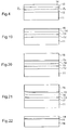
- figure 1 and 2 a set that one seeks to achieve is schematically figure 1 and 2 , the interface (or the layer intermediate) schematized on the figure 2 representing the region in which we will seek to create local differences in the link.
- the figure 3 in particular represents an example of the preparation of a face intended to participate in an interface having, in accordance with the invention, two zones having different mechanical strengths. More precisely, in this example shown, the goal is to obtain a central zone Z1 of mechanical strength E c1 less than that, E c2 , of a peripheral zone Z2, surrounding this central zone.
- SiO 2 / SiO 2 and Si / SiO 2 bonding will be considered.
- suitable chemical treatments for example NH 4 OH / H 2 O 2 / H 2 O (also called SC1) for Si and H 3 PO 4 or HF for Si 3 N 4 ).
- the figure 4 represents the option where the substrate 11 and the thin film 14 are monocrystalline silicon, and where two intermediate layers 12 and 13 have been formed prior to bonding on the substrate 11 and the thin layer 14 respectively.
- layer 14 will be called the active layer, representing the layer that will comprise the components except for some particular cases for which an additional epitaxial layer for example will be deposited on this layer 14.
- the thin layer is obtained by mechanical and / or chemical thinning of the structure.
- SiO 2 / SiO 2 (or Si / SiO 2) bonding it is first possible to use a temporary mask which makes it possible to deposit a protective layer, for example example in nitride Si 3 N 4 , only on the ring of the oxide layer SiO 2 12 and / or 13.
- This oxide layer may have been prepared in several ways (deposition, thermal oxidation of silicon) and have a thickness variable depending on the application. For this example, we can choose a thermal oxide of thickness 1 ⁇ m.
- the surface of the central disk is formed of oxide alone while the surface of the outer ring (typically a few mm wide) is formed, this oxide covered with an additional protective layer (in nitride for example).
- HF etching is then carried out, the purpose of which is to roughen the surface of the oxide, a roughness whose importance will increase with the oxide thickness removed.
- the importance of this roughening can be optimized, especially according to the specifications the process for producing the components (or epitaxial growth) that will have to be formed without delamination and the chosen mode of implementation of the final disassembly.
- HF etching removal with an oxide thickness in the range of a few hundred to a few thousand ⁇ is a good starting compromise.
- a thickness of the order of 1000 ⁇ nitride protects the oxide below any attack by HF. This attack increases the roughness of the central zone of the oxide layer 12 and / or 13.
- the removal of the nitride is then carried out, for example, by etching with hot ortophosphoric acid (H 3 PO 4 ) ( > 110 ° C).
- H 3 PO 4 hot ortophosphoric acid
- the oxide thickness removed becomes important, especially because the application requires (especially in the range of a few thousand A, knowing that 5000 ⁇ is a good starting compromise for many cases), it should be noted that in addition to the desired effect of local increase of the roughness, it results in the creation of a difference in level between the central zone (which has undergone the HF attack) and the crown (which has been preserved of this attack). To obtain a high quality bonding at the crown in combination with a bond of satisfactory quality in the central area, it may be necessary, in some cases, to remove or reduce this difference in level. For this, it may be wise to use a polishing (mechanical-chemical type for example).
- An alternative is to roughen the entire intermediate layer 12 and / or 13, that is to say without protecting the crown, but to add locally at the level of this crown a treatment that will significantly increase the bond strength.
- a treatment that will significantly increase the bond strength.
- These treatments have the advantage of not creating relief.
- Another alternative relates to the use of localized thermal anneals (laser beam, non-uniform furnaces, lamp heating, etc.) after the gluing operation. Indeed, as we can see in C. Maleville et al., Semiconductor wafer bonding, Science Technology and Application IV, PV 97-36, 46 The Electrochemical Society Proceedings Series, Pennington, NJ (1998) ), a difference in annealing temperature after sticking a hundred degrees can lead, especially in the field of temperatures above 800 ° C to a significant variation in the bonding energy.
- This alternative can be used alone or in combination with a roughening of an intermediate layer at least 12 and 13 or only, (ie without any roughening step at all).
- SiO2 / SiO2 bonding is to anneal the entire structure at 1000 ° C but selectively heat the ring at 1200 ° C. Another is not to anneal at all the crown, at a temperature of 1000 ° C.
- selective annealing it is understood that, due to the thermal conduction phenomena and the difficulty in producing equipment that locally warms up with perfect selectivity, localized heating can result in a heat input gradient. In this case, the annealing temperature can be considered as maximum at the edges of the substrate and falling as one approaches the center of the substrate.
- Another variant for producing a removable substrate may be based on a difference of chemical nature between zone Z1 and zone Z2.
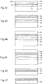
- a protective crown (resin, PECVD deposit, etc.) of a few mm in width is deposited so as to define the dimensions of the zone Z2, as shown in FIG. figure 5 .
- the structure is then etched (wet etching or dry according to the techniques conventionally used to etch silicon) so that this etching only attacks the unprotected region.
- etching only attacks the unprotected region.
- we obtain a recessed silicon wafer at its center possibly with a step of removal of the protective crown), as shown in FIG. figure 6 .
- zone Z1 (hollow disk) and zone Z2 (outer ring).
- an oxide is deposited by CVD.
- the thickness of the deposited oxide layer is much greater than the depth of the recess, leading to the case of the figure 7 .
- a planarizing polishing will eliminate the difference in level between the crown and the center of the structure as well as the high roughness intrinsic to this type of deposit (see figure 8 ). Then, an HF etching is carried out so as to lead to the structure represented in FIG. figure 9 . In this case, the HF etching is stopped when the silicon is flush with a ring.
- a configuration "silicon crown and oxide roughened in the center", which defines an energy differential between Z1 and Z2, on the one hand because these two zones have a different roughness and on the other hand because the nature of materials is different (bonding properties by different molecular adhesion).
- this sequence can be modified to arrive at a "ring silicon and non-rugose oxide in the center" configuration .
- one can for example remove the HF etching step but extend the preliminary polishing step to the outcropping during polishing of the silicon crown.
- the energy differential between Z1 and Z2 is essentially based on the difference in nature of the materials. In this case, the differential is lower.
- the recess and the oxide deposit have been cited in the case where they are made on the substrate 11 (the configuration of the figure 10 ).
- One variant consists in carrying out these operations on the side of the thin layer 14 (see FIG. figure 12 ), or both sides (see figure 11 ).
- This structure has the advantage of having an excellent selectivity with regard to chemical etching between the two materials considered (for example with the aid of HF) which will make it possible to facilitate disassembly by an easy and selective removal by chemical etching of the crown.
- this removable substrate is, depending on the thickness of the active layer processed (that is to say treated so as to make all or part of a component) or not, to allow the separation of the active layer to obtain either a self-supporting layer (relatively thick layer, that this thickness is already present from the manufacture of the removable substrate or during deposition steps subsequent to its manufacture as is the case during an epitaxy step) either a surface layer generally finer carried on a target support, whether the final support or just a temporary support to be disassembled itself.
- a self-supporting layer relatively thick layer, that this thickness is already present from the manufacture of the removable substrate or during deposition steps subsequent to its manufacture as is the case during an epitaxy step
- Such a transfer of the surface layer on the target substrate can be achieved in different ways.
- this transfer can be carried out by a new molecular bonding of what must become the thin layer to be transferred to another substrate.
- the first structure is obtained according to one of the channels described above to lead to the removable substrate corresponding to the figure 4 .
- the monocrystalline silicon layer 14 for this example will be the future active layer.
- the central zone of the bonding layer having been roughened on the one hand before bonding and on the other hand not having undergone a reinforcing heat treatment at very high temperatures (preferably below 1100.degree. even better below 1000 or even 900 ° C), an oxide of 500 ⁇ is formed by thermal oxidation to lead to the structure shown in FIG. figure 19 . This oxide will become the future buried oxide of the second SOI structure.
- This demountable substrate (11 + 12 + 13 + 14 + 15) is, in the example in question, bonded by molecular adhesion to a silicon substrate 16 (see figure 20 ) which will become the future final support of the active layer.
- the stack obtained is preferably stabilized at high temperature (1100 ° C.) to strongly consolidate the second bonding at the interface of the layers 15 and 16.
- This second bonding is conventional in that there is no differentiation. between zones with different mechanical strength.
- the first bonding undergoing the same treatment will have, however, at least in its central part corresponding to the zone Z1 a mechanical strength lower than the second bonding.
- a mechanical and / or chemical method can be used for detachment.
- one begins by plunging the stack obtained in a bath of HF, one of whose goals is to overgrading the oxide 12 and 13 from the edges of the assembly to eliminate the ring corresponding to the zone Z2 and lead to the zone Z1.
- the two interfaces 12/13 and 15/16 will be preferentially attacked.
- the 12/13 interface of the removable substrate is advantageously an oxide / oxide interface. So it spins more easily than the 15/16 interface that is between oxide and silicon.
- the 500 ⁇ buried oxide previously formed on the layer 14 could have been formed on the substrate 16 before bonding and not on the layer 14.
- Another variation had been to divide the thickness of 500 ⁇ into two parts to form a portion on the substrate 16, for example 250 ⁇ , and the other part on the layer 14, 250 ⁇ in the example respectively.
- both molecular bonded interfaces are of the oxide / oxide type
- the stabilization of the second High temperature bonding may have been conducted to ensure that the HF attack is preferentially at the first interface.
- the creation of a zone Z1 with a low mechanical strength made it possible to preferentially separate the complete stack according to the first bonding interface and the zone Z2 made it possible on the one hand to take an active layer 14 of good quality and quality. avoid, on the other hand, crack initiators that can cause yield losses, a decrease in the surface area of the active film due to the peeling of the edge film, and therefore a sharp increase in particulate contamination on the wafers.
- the first operations related to the fabrication of the transistors essentially consist in producing the first gate of the CMOS transistor (see FIG. figure 24 ) according to conventional technology on a removable substrate (see figure 23 ) as described in figure (4 ), identical in all respects to the case described above for the realization of structures SOI buried fine oxide.
- the stabilization temperature of the bonding may optionally be reduced in a temperature range of the order of 900/1000 ° C.
- On this substrate is then deposited (see figure 25 ) an oxide layer of a thickness of the order of one micron by a conventional deposition technique (CVD for example).
- This oxide is planarized according to a conventional mechano-chemical polishing technique (see figure 26 ).
- molecular adhesion is carried out with another silicon substrate 16 (see FIG. figure 27 ).
- This bonding is preferably stabilized at a temperature of 1000 to 1100 ° C if the structures formed for the first grid support it, at temperatures of the order of 900/1000 ° C. otherwise.
- the separation see figure 28 ) identical to the previous case (blade insertion, jet of water under pressure or compressed air etc.).
- the residue of the oxide layer 13 is removed by chemical etching.
- the substrate 16 may be chosen for its electrical insulating properties (high-resistivity silicon, quartz, sapphire, etc.) to provide an ideal support for microwave and telecommunications circuits, thus limiting losses in the substrate.
- the final support a transparent substrate.
- FIG. 29 to 32 Another example of dismantling implementation is briefly described here ( Figures 29 to 32 ) for the realization of circuits on thin substrates.
- the thicknesses of interest in the final are typically below a few hundred ⁇ ms, or even in the order of a few tens of ⁇ ms. They concern, for example, power applications or smart card applications and other circuits for which a certain flexibility is sought (plastic supports, curved supports, etc.).
- the purpose here is to separate, without delay, the layer 14 after completion of the circuits or components C, in the case where this layer 14 is sufficiently thick to be self-supporting but too thin to undergo without damage a circuit making process (typically below a few hundred ⁇ ms, or even of the order of a few tens of ⁇ ms).
- This 645 ⁇ m substrate is then bonded by molecular adhesion, for example, to a 725 ⁇ m plate, leaving areas of lower mechanical strength.
- the plate of 725 microns is then thinned, for example by grinding and chemical mechanical polishing until reaching the desired 80 microns.
- the assembly after assembly therefore corresponds to the standards and sufficiently withstands the manufacturing processes of all or part of the components.
- one of the disassembly techniques mentioned above can be used ( figure 31 ; HF attack and mechanical stresses) with the difference that the substrate 16 can be omitted. In some cases, however, its presence may be interesting.
- the only self-supporting layer 14 represents the final substrate of interest characterized by a substrate with a thickness of 80 ⁇ m comprising the components. The rest of the substrate can be recycled.
- the removable substrate consists of a germanium surface layer having an SiO 2 -SiO 2 bonding interface to undergo an epitaxial temperature of 550 ° C. (a typical case in the case of GaInAs growth constituting a solar cell for space), then the roughness should be advantageously 0.4 nm rms for the substrate to be removable.
- Another example of implementation relates to the realization of chip card circuits for which the flexibility of the support becomes critical, on the one hand because of the increase in the size of the circuits, and on the other hand because the trend is to want cards more and more resistant to deformations.
- a monocrystalline silicon support whose thickness is greater than fifty micros is in this context too brittle because of its excessive thickness when subjected to a bending force such as can regularly undergo a smart card.
- the figure 35 represents a starting set similar to that of the figure 4 , with a starting substrate 11 ', covered with a silicon oxide layer 12', itself bonded by molecular adhesion to a second layer of silicon oxide 13 ', itself covered with a layer 14 'in silicon.
- the circuits are made within the layer 14 'of silicon.
- An adhesive is preferably chosen which makes it possible to obtain a very thin layer 15, while having the highest possible mechanical strength at low temperature, for example ⁇ 400 ° C., in order not to risk damaging the components of the active layer made before this bonding step.
- It may advantageously be thermosetting glues or glues curable by UV radiation (it is sufficient in this case to choose a final substrate 16 'which is transparent to UV).
- the residue of the first substrate, substrate support hitherto referred to as “dismountable” (see FIG. figure 37 ) reusable after, preferably, polishing the layer 12 'and the active layer 14' ( figure 38 ) reported on this other support 16 ', or free variant and self-supporting if the thickness of the layer 14' allows.
- the second substrate 16 ' may alternatively be only an intermediate substrate in a much longer process which will continue or by the pure and simple suppression of this intermediate substrate 16' or by another transfer layer on yet another support, generally with removal of the substrate 16 '.
- the removable substrate obtained using the technique described above is glued, after being "processed” on the intermediate substrate.
- This intermediate substrate may be a rigid or flexible substrate (see the previous examples). If it is rigid it can even be a silicon wafer.
- adhesive bonding it is also possible to envisage the use of adhesive films known to those skilled in the art, in particular to carry out the operations of cutting silicon wafers and encapsulating integrated circuits or else "packaging” or else "back-end” according to two expressions Anglo-Saxon ("blue sticky", Teflon® adhesive films, ..). If this adhesive film is double-sided, it may be wise to stick on the back side of this film, as an intermediate substrate, a substrate or support allowing the stiffening of the assembly at the time of cutting.
- Possible detachment techniques include the application of tensile and / or shear and / or flexural forces. To these applications of forces, it may be advisable to couple a chemical etching of the interface or even other means such as ultrasound.
- the attack of the low energy interface facilitates the spinning of the bonding interface and thus the transfer of the processed layer on the intermediate substrate. Under these conditions, it is advantageous for the processed layers to be protected (for example by an additional nitride deposition in the case of an HF attack).
- the stress application means can be applied directly to the thin film or to the intermediate substrate (handle). They can be mechanical (by inserting a blade at the bonding interface, in particular) and / or by the use of a detachment clip ( WO 00/26000 ) and / or by jet, by the insertion of a gas flow as described in the document FR 2796491 and / or a liquid ( EP 0925888 , EP 0989593 ).
- the removable substrate may advantageously be prepared beforehand (by chemical etching for example) to be able to bring the fluid locally at the gluing interface.
- the intermediate substrate sometimes called “handle” can then be cut (or not), totally or partially (notches or cutting starts) into elements corresponding to electronic components and can be carried on different media.
- This report can be a collective report where all the components, even if they are connected only by a support, are transferred at the same time during the same technological operation or be a report component to component (or chip chip ) if they are the object of after others of this postponement.
- These supports can be plastic as on a smart card and, in this case is advantageously used glue for the report.
- the elements may also be transferred to a plate comprising other electronic or optoelectronic devices and, in this case, the transfer may again employ a molecular adhesion technique (see Figures 4 and 19 to 22 imagining the additional presence of components made in the layer 14).
- the elements can be carried forward by conventional means such as those called "pick and place”.
- the elements can also be transferred to another medium to improve the properties for example from a thermal point of view.
- the thin layer previously glued on its final support, can be separated (element by element, or globally) of its handle by the intermediate of mechanical forces.
- zones Z1 and Z2 may not describe a system consisting of a central circular zone Z1 surrounded by an outer ring Z2.
- the network of squares of the figure 18 can be replaced by other forms of networks (lines, columns, concentric circles, etc.) whose pitch and other geometric dimensions may vary depending on the application and the disassembly technique selected.
- the advantage of adopting a network may be preferable when the structure that will be constructed will impose significant mechanical stresses that will refer to the level of the link interface (in this case a short-range repetition of areas with good mechanical resistance is preferable), or when the layer 14 may have holes, voluntary or not, locally exposing the bonding zone which in turn may be the subject of inadvertent delamination whose epicenter is the hole, or by interest method simplification (for example for cutting into single chips) in the case of the realization of chips.
- dimensions of the order of ⁇ m will be preferred for structures having to undergo a high level of stress (for example, for example).
- a hetero-epitaxy or any other deposit or technological step putting the structure in tension or compression marked) or in the case of small circuits, or circuits made with sub-micron photolithographic resolution.
- scales of the order of mm or even cm are preferable.
- More than two zones can of course be considered (Z1, Z2, Z3, etc.) in many combinations. Beyond a discrete number of zone types with a specific mechanical strength, it is also possible to envisage a continuum of zones characterized by a continuous variation of the mechanical strength. Thus it can be envisaged, for example, that the mechanical strength continuously changes from a maximum value in the vicinity of the edge to a minimum value at its center.
- This variation may or may not have a symmetry of revolution around the axis perpendicular to the plane of the substrate.
- the production methods to achieve this type of substrate and their use during disassembly remain in all respects similar to the descriptions given in the case of the figure 1 to 8 when the geometrical shapes used are adapted (shapes of the masks for forming the protective layers for selective roughening, forms of the masks for selective deposition, form of polishing fabrics which can be designed to preferentially polish concentric rings, etc. ).
- each zone Z2 surrounds or simply runs along the outline of each Z1 zone parcel.
- the surface of the component can correspond exactly with the zone Z1 or on the contrary be higher or even lower, in configurations where one of the surfaces of the component and that of the zone Z1 includes 'other.
- the configuration chosen depends on the technique that will be used during disassembly. These techniques may be the same as those described previously for dismantling a substrate having only a crown Z2 surrounding a central disk Z1.
- An interesting variant consists in using one of the standard component cutting techniques (sawing, laser cutting, etc.) to cut or delimit trenches, at least partially around the chips, parcels, etc.
- FIG 41 Another interesting variation is based on the use of chemical etchings associated with a photolithography operation, to produce identical trenches and / or to cause the removal of the connection zone corresponding to Z2.
- the dotted vertical lines visualize the contour of the desired parcels.
- each plot is peeled off from the substrate, which amounts to consider that the substrate is peeled off from each parcel (alternatively, all the layers can be cut out, ie all the parcels at a time).
- the zone with a high mechanical strength is at the periphery, the risk of delamination during processing steps, for example intended to produce on the layer 3 or 4 electronic, optical or other elements, is reduced, while, when the separation is wanted, it propagates without difficulty, in a controlled manner, in the central zone (it may have been initiated peripherally).
- the zone distribution combination Z1 and Z2 for forming an outer ring at the substrate, as shown in FIG. figure 4 , with a distribution aimed at protecting each of the chips, as shown in figure 13 , is one of the interesting combinations.
- the roughness should be advantageously 0.4 nm rms for the substrate to be removable.
- Another example is that where it is desired to carry out an epitaxial step of an epitaxial stack on a removable substrate. This is particularly the case for the production of blue and white LEDs or laser diodes in thin layers (for example for better extraction of the emitted light or for better heat dissipation through a transfer to a good thermal conductive substrate such than copper or diamond).
- the epitaxial stack considered is based on compound semiconductors derived from GaN (AlN, GaAl, GaAlInN, etc.).
- a method consists in forming, according to one of the methods described previously, a demountable structure equivalent to that of the figure 4 (or the figure 26 or else 35) where the layer 14 is SiC 6H (face Si upwardly shown in the figures), the layers 12 and 13 are, for the example of the figure 4 , Silicon oxides and the substrate 11 is made of polycrystalline (or sapphire) SiC.
- the epitaxial formation of the nitride stack 15 ( figure 43 ).
- This epitaxy can be carried out by epitaxial techniques well known to those skilled in the art under the Anglo-Saxon acronyms of MBE (for Molecular Beam Epitaxy) for a category of them or by MOCVD (Metallo-Organic).
- the epitaxial growth temperatures rarely exceed 600 ° C while the typical temperatures for the second are of the order of 1050-1100 ° C.
- the choice of couples or sets of zones with mechanical strength Z1, Z2, etc. must be optimized.
- one of the previously described methods based on a roughening of the two oxide layers 12 and 13 by HF etching will be chosen.
- An alternative consisting in forming a crown 5 mm wide from the edge of the substrate. This structure is then subject to epitaxial growth MOCVD to achieve at 1100 ° C a stack whose thickness is of the order of 1 .mu.m.
- the structure is annealed before epitaxy, typically in the range of 900 to 1200 ° C to strongly consolidate the mechanical strength of the crown.
- the assembly undergoes oxide deposition, CMP planarization, molecular bonding (for example on a silicon substrate) and annealing at 1100.degree. strengthen this last collage.
- Layer 16 is made ( figure 44 ).
- a separation by mechanical forces is carried out, for example by inserting a blade, by applying a pressurized water jet or compressed air according to for example the techniques described above.
- Final deoxidation finally makes it possible to remove the residue from the oxide layer 13 - figure 46 -.
- at least the SiC layer 14 having served as nucleation layer for the epitaxial stack can be removed by etching ( figure 47 ).
- the realization of diodes can be seen before or after the final transfer.
- the interface between the substrate and what is intended to form the "active" layer may alternatively be formed by a fragile buried layer, formed such micro-cavities, micro-bubbles or “platelets", This method is used with many semiconductor materials or not.
- zones Z1 and Z2 a single crown, definition of plots, networks of zones, multitude of zones, ...), the techniques of dismantling of these structures (by mechanical stresses, chemical treatments, heat treatments, selective removal crowns and zones Z2, %) and their example of implementation, the elements and examples given in section 1 concerning the case of an interface or intermediate layer produced by molecular adhesion remain valid.
- a porous layer may be obtained, in particular from the following materials: Si, GaAs, InP, GaAsP, GaAlAs, InAs, AlGaSb, ZnS, CdTe and SiGe, in forms which may be monocrystalline, polycrystalline or amorphous.
- porous silicon by electrolysis in HF. It is known to vary the porosity of Si by modifying the concentration of HF or by varying the current. For example, the porosity ranges from 2.1 g / cm 3 to 0.6 g / cm 3 by decreasing the HF concentration from 50% to 20%.
- an epitaxy makes it possible to create a monocrystalline layer of Si on this porous layer (see figure 48 , which represents an assembly comprising a substrate 21, the porous layer 22 having controlled differences in porosity between the various zones Z1 'and Z2', and a thin layer 23).
- Hydrogen annealing smoothing anneals are advantageously used before the epitaxy step in order to reseal at least part of the surface of the pores.
- This monocrystalline layer which thus becomes the active layer, depends on the intended applications.
- this active layer can become after disassembly a self-supporting layer (if it is quite thick) or reported on a target substrate (by molecular adhesion for example) (especially for low thicknesses).
- the delamination of the active layer of its substrate can be done chemically or by the introduction of a fluid, locally at the level of the porous layer.
- An alternative may be to not porous periphery on a few mm (case of the figure 49 with a substrate 21 ', a layer 22' of which some areas are porous, and a monocrystalline layer 23 '). he then it becomes advisable to eliminate this ring by cutting (mechanical or laser or chemically by HF / HNO 3 or TMAH).
- zones Z1 and Z2 a single crown, definition of plots, networks of zones, multitude of zones, ...), the techniques of dismantling of these structures (by mechanical stresses, chemical treatments, heat treatments, selective removal crowns and zones Z2, %) and their example of implementation, the elements and examples given in section 1 concerning the case of an interface or intermediate layer produced by molecular adhesion remain valid.
Landscapes
- Engineering & Computer Science (AREA)
- Microelectronics & Electronic Packaging (AREA)
- Power Engineering (AREA)
- General Physics & Mathematics (AREA)
- Computer Hardware Design (AREA)
- Physics & Mathematics (AREA)
- Condensed Matter Physics & Semiconductors (AREA)
- Manufacturing & Machinery (AREA)
- Ceramic Engineering (AREA)
- Recrystallisation Techniques (AREA)
- Element Separation (AREA)
- Mechanical Treatment Of Semiconductor (AREA)
- Laminated Bodies (AREA)
- Materials For Medical Uses (AREA)
- Weting (AREA)
Applications Claiming Priority (3)
| Application Number | Priority Date | Filing Date | Title |
|---|---|---|---|
| FR0105129A FR2823596B1 (fr) | 2001-04-13 | 2001-04-13 | Substrat ou structure demontable et procede de realisation |
| FR0105129 | 2001-04-13 | ||
| PCT/FR2002/001266 WO2002084721A2 (fr) | 2001-04-13 | 2002-04-11 | Substrat ou structure demontable et procede de realisation |
Publications (2)
| Publication Number | Publication Date |
|---|---|
| EP1378003A2 EP1378003A2 (fr) | 2004-01-07 |
| EP1378003B1 true EP1378003B1 (fr) | 2017-11-08 |
Family
ID=8862351
Family Applications (1)
| Application Number | Title | Priority Date | Filing Date |
|---|---|---|---|
| EP02732806.1A Expired - Lifetime EP1378003B1 (fr) | 2001-04-13 | 2002-04-11 | Procede de realisation d'un substrat ou structure demontable |
Country Status (9)
| Country | Link |
|---|---|
| US (1) | US7713369B2 (ja) |
| EP (1) | EP1378003B1 (ja) |
| JP (2) | JP4540933B2 (ja) |
| KR (1) | KR100933897B1 (ja) |
| CN (1) | CN100355025C (ja) |
| AU (1) | AU2002304525A1 (ja) |
| FR (1) | FR2823596B1 (ja) |
| TW (1) | TW577102B (ja) |
| WO (1) | WO2002084721A2 (ja) |
Families Citing this family (114)
| Publication number | Priority date | Publication date | Assignee | Title |
|---|---|---|---|---|
| FR2748851B1 (fr) | 1996-05-15 | 1998-08-07 | Commissariat Energie Atomique | Procede de realisation d'une couche mince de materiau semiconducteur |
| FR2773261B1 (fr) | 1997-12-30 | 2000-01-28 | Commissariat Energie Atomique | Procede pour le transfert d'un film mince comportant une etape de creation d'inclusions |
| FR2823599B1 (fr) * | 2001-04-13 | 2004-12-17 | Commissariat Energie Atomique | Substrat demomtable a tenue mecanique controlee et procede de realisation |
| FR2823596B1 (fr) | 2001-04-13 | 2004-08-20 | Commissariat Energie Atomique | Substrat ou structure demontable et procede de realisation |
| FR2846788B1 (fr) * | 2002-10-30 | 2005-06-17 | Procede de fabrication de substrats demontables | |
| FR2847077B1 (fr) * | 2002-11-12 | 2006-02-17 | Soitec Silicon On Insulator | Composants semi-conducteurs, et notamment de type soi mixtes, et procede de realisation |
| FR2848336B1 (fr) * | 2002-12-09 | 2005-10-28 | Commissariat Energie Atomique | Procede de realisation d'une structure contrainte destinee a etre dissociee |
| US20090325362A1 (en) * | 2003-01-07 | 2009-12-31 | Nabil Chhaimi | Method of recycling an epitaxied donor wafer |
| FR2892228B1 (fr) * | 2005-10-18 | 2008-01-25 | Soitec Silicon On Insulator | Procede de recyclage d'une plaquette donneuse epitaxiee |
| EP1437426A1 (de) * | 2003-01-10 | 2004-07-14 | Siemens Aktiengesellschaft | Verfahren zum Herstellen von einkristallinen Strukturen |
| US6759277B1 (en) * | 2003-02-27 | 2004-07-06 | Sharp Laboratories Of America, Inc. | Crystalline silicon die array and method for assembling crystalline silicon sheets onto substrates |
| US7122095B2 (en) | 2003-03-14 | 2006-10-17 | S.O.I.Tec Silicon On Insulator Technologies S.A. | Methods for forming an assembly for transfer of a useful layer |
| FR2852445B1 (fr) * | 2003-03-14 | 2005-05-20 | Soitec Silicon On Insulator | Procede de realisation de substrats ou composants sur substrats avec transfert de couche utile, pour la microelectronique, l'optoelectronique ou l'optique |
| JP4794810B2 (ja) * | 2003-03-20 | 2011-10-19 | シャープ株式会社 | 半導体装置の製造方法 |
| FR2856844B1 (fr) * | 2003-06-24 | 2006-02-17 | Commissariat Energie Atomique | Circuit integre sur puce de hautes performances |
| JP4581349B2 (ja) * | 2003-08-29 | 2010-11-17 | 株式会社Sumco | 貼合せsoiウェーハの製造方法 |
| US8475693B2 (en) | 2003-09-30 | 2013-07-02 | Soitec | Methods of making substrate structures having a weakened intermediate layer |
| FR2860249B1 (fr) * | 2003-09-30 | 2005-12-09 | Michel Bruel | Procede de fabrication d'une structure en forme de plaque, en particulier en silicium, application de procede, et structure en forme de plaque, en particulier en silicium |
| JP4809600B2 (ja) * | 2003-10-28 | 2011-11-09 | 株式会社半導体エネルギー研究所 | 半導体装置の作製方法 |
| FR2861497B1 (fr) * | 2003-10-28 | 2006-02-10 | Soitec Silicon On Insulator | Procede de transfert catastrophique d'une couche fine apres co-implantation |
| FR2871291B1 (fr) * | 2004-06-02 | 2006-12-08 | Tracit Technologies | Procede de transfert de plaques |
| JP4838504B2 (ja) * | 2004-09-08 | 2011-12-14 | キヤノン株式会社 | 半導体装置の製造方法 |
| FR2876220B1 (fr) * | 2004-10-06 | 2007-09-28 | Commissariat Energie Atomique | Procede d'elaboration de structures empilees mixtes, a zones isolantes diverses et/ou zones de conduction electrique verticale localisees. |
| US7405108B2 (en) * | 2004-11-20 | 2008-07-29 | International Business Machines Corporation | Methods for forming co-planar wafer-scale chip packages |
| FR2878648B1 (fr) * | 2004-11-30 | 2007-02-02 | Commissariat Energie Atomique | Support semi-conducteur rectangulaire pour la microelectronique et procede de realisation d'un tel support |
| FR2880189B1 (fr) | 2004-12-24 | 2007-03-30 | Tracit Technologies Sa | Procede de report d'un circuit sur un plan de masse |
| JP2006216891A (ja) * | 2005-02-07 | 2006-08-17 | Tokyo Univ Of Agriculture & Technology | 薄膜素子構造の作製方法、及び薄膜素子構造作製用の機能性基体 |
| KR20080003002A (ko) * | 2005-04-27 | 2008-01-04 | 린텍 가부시키가이샤 | 시트상 언더필재 및 반도체장치의 제조방법 |
| FR2888400B1 (fr) * | 2005-07-08 | 2007-10-19 | Soitec Silicon On Insulator | Procede de prelevement de couche |
| FR2889887B1 (fr) * | 2005-08-16 | 2007-11-09 | Commissariat Energie Atomique | Procede de report d'une couche mince sur un support |
| FR2891281B1 (fr) * | 2005-09-28 | 2007-12-28 | Commissariat Energie Atomique | Procede de fabrication d'un element en couches minces. |
| EP1777735A3 (fr) * | 2005-10-18 | 2009-08-19 | S.O.I.Tec Silicon on Insulator Technologies | Procédé de recyclage d'une plaquette donneuse épitaxiée |
| FR2893750B1 (fr) * | 2005-11-22 | 2008-03-14 | Commissariat Energie Atomique | Procede de fabrication d'un dispositif electronique flexible du type ecran comportant une pluralite de composants en couches minces. |
| EP1801870A1 (en) * | 2005-12-22 | 2007-06-27 | Princo Corp. | Partial adherent temporary substrate and method of using the same |
| US7781309B2 (en) * | 2005-12-22 | 2010-08-24 | Sumco Corporation | Method for manufacturing direct bonded SOI wafer and direct bonded SOI wafer manufactured by the method |
| TWI285424B (en) * | 2005-12-22 | 2007-08-11 | Princo Corp | Substrate including a multi-layer interconnection structure, methods of manufacturing and recycling the same, method of packaging electronic devices by using the same, and method of manufacturing an interconnection device |
| US7829436B2 (en) | 2005-12-22 | 2010-11-09 | Sumco Corporation | Process for regeneration of a layer transferred wafer and regenerated layer transferred wafer |
| CN1996582B (zh) * | 2006-01-06 | 2012-02-15 | 巨擘科技股份有限公司 | 包含多层内连线结构的载板及其制造、回收以及应用方法 |
| DE102006059394B4 (de) * | 2006-12-08 | 2019-11-21 | Institut Für Mikroelektronik Stuttgart | Integrierte Schaltung und Verfahren zu deren Herstellung |
| DE102006013419B4 (de) * | 2006-03-14 | 2008-05-29 | Institut Für Mikroelektronik Stuttgart | Verfahren zum Herstellen einer integrierten Schaltung |
| WO2007104443A1 (de) * | 2006-03-14 | 2007-09-20 | Institut Für Mikroelektronik Stuttgart | Verfahren zum herstellen einer integrierten schaltung |
| US8051557B2 (en) | 2006-03-31 | 2011-11-08 | Princo Corp. | Substrate with multi-layer interconnection structure and method of manufacturing the same |
| US20080057678A1 (en) * | 2006-08-31 | 2008-03-06 | Kishor Purushottam Gadkaree | Semiconductor on glass insulator made using improved hydrogen reduction process |
| FR2910179B1 (fr) | 2006-12-19 | 2009-03-13 | Commissariat Energie Atomique | PROCEDE DE FABRICATION DE COUCHES MINCES DE GaN PAR IMPLANTATION ET RECYCLAGE D'UN SUBSTRAT DE DEPART |
| FR2912839B1 (fr) * | 2007-02-16 | 2009-05-15 | Soitec Silicon On Insulator | Amelioration de la qualite de l'interface de collage par nettoyage froid et collage a chaud |
| FR2913968B1 (fr) | 2007-03-23 | 2009-06-12 | Soitec Silicon On Insulator | Procede de realisation de membranes autoportees. |
| WO2008123117A1 (en) * | 2007-03-26 | 2008-10-16 | Semiconductor Energy Laboratory Co., Ltd. | Soi substrate and method for manufacturing soi substrate |
| FR2914493B1 (fr) | 2007-03-28 | 2009-08-07 | Soitec Silicon On Insulator | Substrat demontable. |
| US7605054B2 (en) | 2007-04-18 | 2009-10-20 | S.O.I.Tec Silicon On Insulator Technologies | Method of forming a device wafer with recyclable support |
| FR2922359B1 (fr) * | 2007-10-12 | 2009-12-18 | Commissariat Energie Atomique | Procede de fabrication d'une structure micro-electronique impliquant un collage moleculaire |
| FR2925221B1 (fr) * | 2007-12-17 | 2010-02-19 | Commissariat Energie Atomique | Procede de transfert d'une couche mince |
| FR2926671B1 (fr) * | 2008-01-17 | 2010-04-02 | Soitec Silicon On Insulator | Procede de traitement de defauts lors de collage de plaques |
| FR2926672B1 (fr) * | 2008-01-21 | 2010-03-26 | Soitec Silicon On Insulator | Procede de fabrication de couches de materiau epitaxie |
| EP2238618B1 (en) * | 2008-01-24 | 2015-07-29 | Brewer Science, Inc. | Method for reversibly mounting a device wafer to a carrier substrate |
| FR2929758B1 (fr) * | 2008-04-07 | 2011-02-11 | Commissariat Energie Atomique | Procede de transfert a l'aide d'un substrat ferroelectrique |
| TWI424587B (zh) * | 2008-06-30 | 2014-01-21 | Luxtaltek Corp | Light emitting diodes with nanoscale surface structure and embossing molds forming nanometer scale surface structures |
| JP5478199B2 (ja) * | 2008-11-13 | 2014-04-23 | 株式会社半導体エネルギー研究所 | 半導体装置の作製方法 |
| US7927975B2 (en) * | 2009-02-04 | 2011-04-19 | Micron Technology, Inc. | Semiconductor material manufacture |
| FR2947098A1 (fr) | 2009-06-18 | 2010-12-24 | Commissariat Energie Atomique | Procede de transfert d'une couche mince sur un substrat cible ayant un coefficient de dilatation thermique different de celui de la couche mince |
| US9847243B2 (en) | 2009-08-27 | 2017-12-19 | Corning Incorporated | Debonding a glass substrate from carrier using ultrasonic wave |
| US8187901B2 (en) | 2009-12-07 | 2012-05-29 | Micron Technology, Inc. | Epitaxial formation support structures and associated methods |
| CN105821435B (zh) | 2010-01-27 | 2018-10-16 | 耶鲁大学 | 用于GaN装置的基于导电性的选择性蚀刻和其应用 |
| WO2011120537A1 (de) * | 2010-03-31 | 2011-10-06 | Ev Group E. Thallner Gmbh | Verfahren zur herstellung eines doppelseitig mit chips bestückten wafers |
| US8852391B2 (en) * | 2010-06-21 | 2014-10-07 | Brewer Science Inc. | Method and apparatus for removing a reversibly mounted device wafer from a carrier substrate |
| JP5677430B2 (ja) * | 2010-07-30 | 2015-02-25 | 京セラ株式会社 | 複合基板、電子部品、ならびに複合基板および電子部品の製造方法 |
| US9263314B2 (en) | 2010-08-06 | 2016-02-16 | Brewer Science Inc. | Multiple bonding layers for thin-wafer handling |
| JP5902917B2 (ja) * | 2010-11-12 | 2016-04-13 | 株式会社半導体エネルギー研究所 | 半導体基板の作製方法 |
| JP5926527B2 (ja) * | 2011-10-17 | 2016-05-25 | 信越化学工業株式会社 | 透明soiウェーハの製造方法 |
| WO2015157202A1 (en) | 2014-04-09 | 2015-10-15 | Corning Incorporated | Device modified substrate article and methods for making |
| US8975157B2 (en) * | 2012-02-08 | 2015-03-10 | Advanced Semiconductor Engineering, Inc. | Carrier bonding and detaching processes for a semiconductor wafer |
| US10543662B2 (en) | 2012-02-08 | 2020-01-28 | Corning Incorporated | Device modified substrate article and methods for making |
| CN104471360B (zh) * | 2012-06-18 | 2016-04-20 | 松下知识产权经营株式会社 | 红外线检测装置 |
| WO2014004261A1 (en) | 2012-06-28 | 2014-01-03 | Yale University | Lateral electrochemical etching of iii-nitride materials for microfabrication |
| CN104507853B (zh) | 2012-07-31 | 2016-11-23 | 索泰克公司 | 形成半导体设备的方法 |
| WO2014026292A1 (en) * | 2012-08-15 | 2014-02-20 | Mcmaster University | Arbitrarily thin ultra smooth film with built-in separation ability and method of forming the same |
| KR101392133B1 (ko) * | 2012-08-20 | 2014-05-07 | 세종대학교산학협력단 | 서로 다른 젖음성을 갖는 영역들을 구비하는 캐리어 기판, 이를 사용한 소자 기판 처리 방법 |
| FR2995447B1 (fr) | 2012-09-07 | 2014-09-05 | Soitec Silicon On Insulator | Procede de separation d'au moins deux substrats selon une interface choisie |
| FR2995445B1 (fr) * | 2012-09-07 | 2016-01-08 | Soitec Silicon On Insulator | Procede de fabrication d'une structure en vue d'une separation ulterieure |
| US10086584B2 (en) | 2012-12-13 | 2018-10-02 | Corning Incorporated | Glass articles and methods for controlled bonding of glass sheets with carriers |
| US9340443B2 (en) | 2012-12-13 | 2016-05-17 | Corning Incorporated | Bulk annealing of glass sheets |
| TWI617437B (zh) | 2012-12-13 | 2018-03-11 | 康寧公司 | 促進控制薄片與載體間接合之處理 |
| US10014177B2 (en) | 2012-12-13 | 2018-07-03 | Corning Incorporated | Methods for processing electronic devices |
| DE102012112989A1 (de) * | 2012-12-21 | 2014-06-26 | Ev Group E. Thallner Gmbh | Verfahren zum Aufbringen einer Temporärbondschicht |
| US9028628B2 (en) | 2013-03-14 | 2015-05-12 | International Business Machines Corporation | Wafer-to-wafer oxide fusion bonding |
| US9058974B2 (en) | 2013-06-03 | 2015-06-16 | International Business Machines Corporation | Distorting donor wafer to corresponding distortion of host wafer |
| JP2015035453A (ja) * | 2013-08-07 | 2015-02-19 | アズビル株式会社 | ウエハ |
| US10510576B2 (en) | 2013-10-14 | 2019-12-17 | Corning Incorporated | Carrier-bonding methods and articles for semiconductor and interposer processing |
| US10381224B2 (en) * | 2014-01-23 | 2019-08-13 | Arizona Board Of Regents On Behalf Of Arizona State University | Method of providing an electronic device and electronic device thereof |
| WO2017034645A2 (en) * | 2015-06-09 | 2017-03-02 | ARIZONA BOARD OF REGENTS, a body corporate for THE STATE OF ARIZONA for and on behalf of ARIZONA STATE UNIVERSITY | Method of providing an electronic device and electronic device thereof |
| JP6770432B2 (ja) | 2014-01-27 | 2020-10-14 | コーニング インコーポレイテッド | 薄いシートの担体との制御された結合のための物品および方法 |
| FR3019374A1 (fr) * | 2014-03-28 | 2015-10-02 | Soitec Silicon On Insulator | Procede de separation et de transfert de couches |
| US11095096B2 (en) | 2014-04-16 | 2021-08-17 | Yale University | Method for a GaN vertical microcavity surface emitting laser (VCSEL) |
| WO2016054232A1 (en) | 2014-09-30 | 2016-04-07 | Yale University | A METHOD FOR GaN VERTICAL MICROCAVITY SURFACE EMITTING LASER (VCSEL) |
| US11018231B2 (en) | 2014-12-01 | 2021-05-25 | Yale University | Method to make buried, highly conductive p-type III-nitride layers |
| EP3298624B1 (en) | 2015-05-19 | 2023-04-19 | Yale University | A method and device concerning iii-nitride edge emitting laser diode of high confinement factor with lattice matched cladding layer |
| KR102573207B1 (ko) | 2015-05-19 | 2023-08-31 | 코닝 인코포레이티드 | 시트와 캐리어의 결합을 위한 물품 및 방법 |
| US11905201B2 (en) | 2015-06-26 | 2024-02-20 | Corning Incorporated | Methods and articles including a sheet and a carrier |
| KR20170033163A (ko) | 2015-09-16 | 2017-03-24 | 임종순 | 수로관 및 이의 시공방법 |
| DE102016106351A1 (de) * | 2016-04-07 | 2017-10-12 | Ev Group E. Thallner Gmbh | Verfahren und Vorrichtung zum Bonden zweier Substrate |
| US20180019169A1 (en) * | 2016-07-12 | 2018-01-18 | QMAT, Inc. | Backing substrate stabilizing donor substrate for implant or reclamation |
| TW202216444A (zh) | 2016-08-30 | 2022-05-01 | 美商康寧公司 | 用於片材接合的矽氧烷電漿聚合物 |
| TWI810161B (zh) | 2016-08-31 | 2023-08-01 | 美商康寧公司 | 具以可控制式黏結的薄片之製品及製作其之方法 |
| FR3063176A1 (fr) * | 2017-02-17 | 2018-08-24 | Soitec | Masquage d'une zone au bord d'un substrat donneur lors d'une etape d'implantation ionique |
| TWI756384B (zh) * | 2017-03-16 | 2022-03-01 | 美商康寧公司 | 用於大量轉移微型led的方法及製程 |
| KR102179165B1 (ko) | 2017-11-28 | 2020-11-16 | 삼성전자주식회사 | 캐리어 기판 및 상기 캐리어 기판을 이용한 반도체 패키지의 제조방법 |
| FR3074960B1 (fr) | 2017-12-07 | 2019-12-06 | Soitec | Procede de transfert d'une couche utilisant une structure demontable |
| US11331692B2 (en) | 2017-12-15 | 2022-05-17 | Corning Incorporated | Methods for treating a substrate and method for making articles comprising bonded sheets |
| KR20200130816A (ko) * | 2018-03-14 | 2020-11-20 | 도쿄엘렉트론가부시키가이샤 | 기판 처리 시스템, 기판 처리 방법 및 컴퓨터 기억 매체 |
| TWI791099B (zh) * | 2018-03-29 | 2023-02-01 | 日商日本碍子股份有限公司 | 接合體及彈性波元件 |
| US10964664B2 (en) | 2018-04-20 | 2021-03-30 | Invensas Bonding Technologies, Inc. | DBI to Si bonding for simplified handle wafer |
| US11101158B1 (en) * | 2018-08-08 | 2021-08-24 | United States Of America As Represented By The Administrator Of Nasa | Wafer-scale membrane release laminates, devices and processes |
| US11081392B2 (en) * | 2018-09-28 | 2021-08-03 | Taiwan Semiconductor Manufacturing Co., Ltd. | Dicing method for stacked semiconductor devices |
| FR3108439B1 (fr) | 2020-03-23 | 2022-02-11 | Soitec Silicon On Insulator | Procede de fabrication d’une structure empilee |
| FR3109016B1 (fr) | 2020-04-01 | 2023-12-01 | Soitec Silicon On Insulator | Structure demontable et procede de transfert d’une couche mettant en œuvre ladite structure demontable |
Citations (1)
| Publication number | Priority date | Publication date | Assignee | Title |
|---|---|---|---|---|
| WO2001004933A1 (fr) * | 1999-07-12 | 2001-01-18 | Commissariat A L'energie Atomique | Procede de decollement de deux elements et dispositif pour sa mise en oeuvre |
Family Cites Families (97)
| Publication number | Priority date | Publication date | Assignee | Title |
|---|---|---|---|---|
| US4121334A (en) | 1974-12-17 | 1978-10-24 | P. R. Mallory & Co. Inc. | Application of field-assisted bonding to the mass production of silicon type pressure transducers |
| JPS53104156A (en) | 1977-02-23 | 1978-09-11 | Hitachi Ltd | Manufacture for semiconductor device |
| US4179324A (en) | 1977-11-28 | 1979-12-18 | Spire Corporation | Process for fabricating thin film and glass sheet laminate |
| JPS5831519A (ja) | 1981-08-18 | 1983-02-24 | Toshiba Corp | 半導体装置の製造方法 |
| SU1282757A1 (ru) | 1983-12-30 | 2000-06-27 | Институт Ядерной Физики Ан Казсср | Способ изготовления тонких пластин кремния |
| JPS62265717A (ja) | 1986-05-13 | 1987-11-18 | Nippon Telegr & Teleph Corp <Ntt> | ガリウムひ素集積回路用基板の熱処理方法 |
| GB8725497D0 (en) | 1987-10-30 | 1987-12-02 | Atomic Energy Authority Uk | Isolation of silicon |
| JP2927277B2 (ja) | 1988-12-05 | 1999-07-28 | 住友電気工業株式会社 | 車載ナビゲータ |
| JPH0355822A (ja) | 1989-07-25 | 1991-03-11 | Shin Etsu Handotai Co Ltd | 半導体素子形成用基板の製造方法 |
| US5013681A (en) | 1989-09-29 | 1991-05-07 | The United States Of America As Represented By The Secretary Of The Navy | Method of producing a thin silicon-on-insulator layer |
| US5310446A (en) | 1990-01-10 | 1994-05-10 | Ricoh Company, Ltd. | Method for producing semiconductor film |
| US5034343A (en) | 1990-03-08 | 1991-07-23 | Harris Corporation | Manufacturing ultra-thin wafer using a handle wafer |
| JPH0719739B2 (ja) | 1990-09-10 | 1995-03-06 | 信越半導体株式会社 | 接合ウェーハの製造方法 |
| US5618739A (en) | 1990-11-15 | 1997-04-08 | Seiko Instruments Inc. | Method of making light valve device using semiconductive composite substrate |
| JPH04199504A (ja) | 1990-11-28 | 1992-07-20 | Mitsubishi Electric Corp | 半導体装置の製造方法 |
| JP2812405B2 (ja) | 1991-03-15 | 1998-10-22 | 信越半導体株式会社 | 半導体基板の製造方法 |
| US5256581A (en) | 1991-08-28 | 1993-10-26 | Motorola, Inc. | Silicon film with improved thickness control |
| JP3416163B2 (ja) | 1992-01-31 | 2003-06-16 | キヤノン株式会社 | 半導体基板及びその作製方法 |
| JPH05235312A (ja) | 1992-02-19 | 1993-09-10 | Fujitsu Ltd | 半導体基板及びその製造方法 |
| JP3352118B2 (ja) * | 1992-08-25 | 2002-12-03 | キヤノン株式会社 | 半導体装置及びその製造方法 |
| US5234535A (en) | 1992-12-10 | 1993-08-10 | International Business Machines Corporation | Method of producing a thin silicon-on-insulator layer |
| JPH07211876A (ja) * | 1994-01-21 | 1995-08-11 | Canon Inc | 半導体基体の作成方法 |
| FR2715501B1 (fr) * | 1994-01-26 | 1996-04-05 | Commissariat Energie Atomique | Procédé de dépôt de lames semiconductrices sur un support. |
| FR2715502B1 (fr) | 1994-01-26 | 1996-04-05 | Commissariat Energie Atomique | Structure présentant des cavités et procédé de réalisation d'une telle structure. |
| FR2715503B1 (fr) | 1994-01-26 | 1996-04-05 | Commissariat Energie Atomique | Substrat pour composants intégrés comportant une couche mince et son procédé de réalisation. |
| JP3293736B2 (ja) | 1996-02-28 | 2002-06-17 | キヤノン株式会社 | 半導体基板の作製方法および貼り合わせ基体 |
| JP3257580B2 (ja) | 1994-03-10 | 2002-02-18 | キヤノン株式会社 | 半導体基板の作製方法 |
| JPH0817777A (ja) | 1994-07-01 | 1996-01-19 | Mitsubishi Materials Shilicon Corp | シリコンウェーハの洗浄方法 |
| JPH0851103A (ja) | 1994-08-08 | 1996-02-20 | Fuji Electric Co Ltd | 薄膜の生成方法 |
| US5567654A (en) | 1994-09-28 | 1996-10-22 | International Business Machines Corporation | Method and workpiece for connecting a thin layer to a monolithic electronic module's surface and associated module packaging |
| JPH08133878A (ja) * | 1994-11-11 | 1996-05-28 | Mitsubishi Materials Corp | グレーズドセラミック基板の製造方法 |
| ATE216802T1 (de) | 1994-12-12 | 2002-05-15 | Advanced Micro Devices Inc | Verfahren zur herstellung vergrabener oxidschichten |
| JP3381443B2 (ja) | 1995-02-02 | 2003-02-24 | ソニー株式会社 | 基体から半導体層を分離する方法、半導体素子の製造方法およびsoi基板の製造方法 |
| CN1132223C (zh) | 1995-10-06 | 2003-12-24 | 佳能株式会社 | 半导体衬底及其制造方法 |
| FR2744285B1 (fr) | 1996-01-25 | 1998-03-06 | Commissariat Energie Atomique | Procede de transfert d'une couche mince d'un substrat initial sur un substrat final |
| FR2747506B1 (fr) | 1996-04-11 | 1998-05-15 | Commissariat Energie Atomique | Procede d'obtention d'un film mince de materiau semiconducteur comprenant notamment des composants electroniques |
| FR2748850B1 (fr) | 1996-05-15 | 1998-07-24 | Commissariat Energie Atomique | Procede de realisation d'un film mince de materiau solide et applications de ce procede |
| FR2748851B1 (fr) | 1996-05-15 | 1998-08-07 | Commissariat Energie Atomique | Procede de realisation d'une couche mince de materiau semiconducteur |
| JP4001650B2 (ja) | 1996-05-16 | 2007-10-31 | 株式会社リコー | 画像形成装置 |
| SG65697A1 (en) | 1996-11-15 | 1999-06-22 | Canon Kk | Process for producing semiconductor article |
| US6054363A (en) | 1996-11-15 | 2000-04-25 | Canon Kabushiki Kaisha | Method of manufacturing semiconductor article |
| DE19648501A1 (de) | 1996-11-22 | 1998-05-28 | Max Planck Gesellschaft | Verfahren für die lösbare Verbindung und anschließende Trennung reversibel gebondeter und polierter Scheiben sowie eine Waferstruktur und Wafer |
| KR100232886B1 (ko) | 1996-11-23 | 1999-12-01 | 김영환 | Soi 웨이퍼 제조방법 |
| DE19648759A1 (de) | 1996-11-25 | 1998-05-28 | Max Planck Gesellschaft | Verfahren zur Herstellung von Mikrostrukturen sowie Mikrostruktur |
| JPH10163166A (ja) * | 1996-11-28 | 1998-06-19 | Mitsubishi Electric Corp | 半導体装置の製造方法及び製造装置 |
| FR2756847B1 (fr) | 1996-12-09 | 1999-01-08 | Commissariat Energie Atomique | Procede de separation d'au moins deux elements d'une structure en contact entre eux par implantation ionique |
| KR100304161B1 (ko) | 1996-12-18 | 2001-11-30 | 미다라이 후지오 | 반도체부재의제조방법 |
| JP3962465B2 (ja) | 1996-12-18 | 2007-08-22 | キヤノン株式会社 | 半導体部材の製造方法 |
| FR2758907B1 (fr) * | 1997-01-27 | 1999-05-07 | Commissariat Energie Atomique | Procede d'obtention d'un film mince, notamment semiconducteur, comportant une zone protegee des ions, et impliquant une etape d'implantation ionique |
| JP3114643B2 (ja) | 1997-02-20 | 2000-12-04 | 日本電気株式会社 | 半導体基板の構造および製造方法 |
| US6033974A (en) | 1997-05-12 | 2000-03-07 | Silicon Genesis Corporation | Method for controlled cleaving process |
| US6013563A (en) | 1997-05-12 | 2000-01-11 | Silicon Genesis Corporation | Controlled cleaning process |
| US5877070A (en) | 1997-05-31 | 1999-03-02 | Max-Planck Society | Method for the transfer of thin layers of monocrystalline material to a desirable substrate |
| EP0996967B1 (de) | 1997-06-30 | 2008-11-19 | Max-Planck-Gesellschaft zur Förderung der Wissenschaften e.V. | Verfahren zur Herstellung von schichtartigen Gebilden auf einem Halbleitersubstrat, Halbleitersubstrat sowie mittels des Verfahrens hergestellte Halbleiterbauelemente |
| US6054369A (en) | 1997-06-30 | 2000-04-25 | Intersil Corporation | Lifetime control for semiconductor devices |
| US6534380B1 (en) | 1997-07-18 | 2003-03-18 | Denso Corporation | Semiconductor substrate and method of manufacturing the same |
| JPH1145862A (ja) | 1997-07-24 | 1999-02-16 | Denso Corp | 半導体基板の製造方法 |
| US6103599A (en) | 1997-07-25 | 2000-08-15 | Silicon Genesis Corporation | Planarizing technique for multilayered substrates |
| FR2767416B1 (fr) | 1997-08-12 | 1999-10-01 | Commissariat Energie Atomique | Procede de fabrication d'un film mince de materiau solide |
| FR2767604B1 (fr) * | 1997-08-19 | 2000-12-01 | Commissariat Energie Atomique | Procede de traitement pour le collage moleculaire et le decollage de deux structures |
| JPH1174208A (ja) | 1997-08-27 | 1999-03-16 | Denso Corp | 半導体基板の製造方法 |
| JP3412470B2 (ja) | 1997-09-04 | 2003-06-03 | 三菱住友シリコン株式会社 | Soi基板の製造方法 |
| US5981400A (en) | 1997-09-18 | 1999-11-09 | Cornell Research Foundation, Inc. | Compliant universal substrate for epitaxial growth |
| JP2998724B2 (ja) | 1997-11-10 | 2000-01-11 | 日本電気株式会社 | 張り合わせsoi基板の製造方法 |
| FR2771852B1 (fr) * | 1997-12-02 | 1999-12-31 | Commissariat Energie Atomique | Procede de transfert selectif d'une microstructure, formee sur un substrat initial, vers un substrat final |
| FR2773261B1 (fr) | 1997-12-30 | 2000-01-28 | Commissariat Energie Atomique | Procede pour le transfert d'un film mince comportant une etape de creation d'inclusions |
| FR2774510B1 (fr) | 1998-02-02 | 2001-10-26 | Soitec Silicon On Insulator | Procede de traitement de substrats, notamment semi-conducteurs |
| MY118019A (en) * | 1998-02-18 | 2004-08-30 | Canon Kk | Composite member, its separation method, and preparation method of semiconductor substrate by utilization thereof |
| JP3031904B2 (ja) * | 1998-02-18 | 2000-04-10 | キヤノン株式会社 | 複合部材とその分離方法、及びそれを利用した半導体基体の製造方法 |
| JP3809733B2 (ja) | 1998-02-25 | 2006-08-16 | セイコーエプソン株式会社 | 薄膜トランジスタの剥離方法 |
| US6057212A (en) | 1998-05-04 | 2000-05-02 | International Business Machines Corporation | Method for making bonded metal back-plane substrates |
| US6054370A (en) | 1998-06-30 | 2000-04-25 | Intel Corporation | Method of delaminating a pre-fabricated transistor layer from a substrate for placement on another wafer |
| US6271101B1 (en) | 1998-07-29 | 2001-08-07 | Semiconductor Energy Laboratory Co., Ltd. | Process for production of SOI substrate and process for production of semiconductor device |
| US6118181A (en) | 1998-07-29 | 2000-09-12 | Agilent Technologies, Inc. | System and method for bonding wafers |
| FR2781925B1 (fr) | 1998-07-30 | 2001-11-23 | Commissariat Energie Atomique | Transfert selectif d'elements d'un support vers un autre support |
| EP0989593A3 (en) | 1998-09-25 | 2002-01-02 | Canon Kabushiki Kaisha | Substrate separating apparatus and method, and substrate manufacturing method |
| FR2784795B1 (fr) | 1998-10-16 | 2000-12-01 | Commissariat Energie Atomique | Structure comportant une couche mince de materiau composee de zones conductrices et de zones isolantes et procede de fabrication d'une telle structure |
| FR2789518B1 (fr) | 1999-02-10 | 2003-06-20 | Commissariat Energie Atomique | Structure multicouche a contraintes internes controlees et procede de realisation d'une telle structure |
| AU4481100A (en) | 1999-04-21 | 2000-11-02 | Silicon Genesis Corporation | Treatment method of cleaved film for the manufacture of substrates |
| JP2001015721A (ja) | 1999-04-30 | 2001-01-19 | Canon Inc | 複合部材の分離方法及び薄膜の製造方法 |
| US6664169B1 (en) | 1999-06-08 | 2003-12-16 | Canon Kabushiki Kaisha | Process for producing semiconductor member, process for producing solar cell, and anodizing apparatus |
| US6362082B1 (en) * | 1999-06-28 | 2002-03-26 | Intel Corporation | Methodology for control of short channel effects in MOS transistors |
| WO2001011930A2 (en) | 1999-08-10 | 2001-02-15 | Silicon Genesis Corporation | A cleaving process to fabricate multilayered substrates using low implantation doses |
| DE19958803C1 (de) | 1999-12-07 | 2001-08-30 | Fraunhofer Ges Forschung | Verfahren und Vorrichtung zum Handhaben von Halbleitersubstraten bei der Prozessierung und/oder Bearbeitung |
| FR2811807B1 (fr) | 2000-07-12 | 2003-07-04 | Commissariat Energie Atomique | Procede de decoupage d'un bloc de materiau et de formation d'un film mince |
| FR2818010B1 (fr) | 2000-12-08 | 2003-09-05 | Commissariat Energie Atomique | Procede de realisation d'une couche mince impliquant l'introduction d'especes gazeuses |
| US6774010B2 (en) | 2001-01-25 | 2004-08-10 | International Business Machines Corporation | Transferable device-containing layer for silicon-on-insulator applications |
| FR2823373B1 (fr) | 2001-04-10 | 2005-02-04 | Soitec Silicon On Insulator | Dispositif de coupe de couche d'un substrat, et procede associe |
| FR2823596B1 (fr) | 2001-04-13 | 2004-08-20 | Commissariat Energie Atomique | Substrat ou structure demontable et procede de realisation |
| US6759282B2 (en) | 2001-06-12 | 2004-07-06 | International Business Machines Corporation | Method and structure for buried circuits and devices |
| US6645831B1 (en) | 2002-05-07 | 2003-11-11 | Intel Corporation | Thermally stable crystalline defect-free germanium bonded to silicon and silicon dioxide |
| US7535100B2 (en) | 2002-07-12 | 2009-05-19 | The United States Of America As Represented By The Secretary Of The Navy | Wafer bonding of thinned electronic materials and circuits to high performance substrates |
| JP4199504B2 (ja) | 2002-09-24 | 2008-12-17 | イーグル工業株式会社 | 摺動部品及びその製造方法 |
| US7071077B2 (en) | 2003-03-26 | 2006-07-04 | S.O.I.Tec Silicon On Insulator Technologies S.A. | Method for preparing a bonding surface of a semiconductor layer of a wafer |
| FR2855910B1 (fr) | 2003-06-06 | 2005-07-15 | Commissariat Energie Atomique | Procede d'obtention d'une couche tres mince par amincissement par auto-portage provoque |
| FR2876219B1 (fr) | 2004-10-06 | 2006-11-24 | Commissariat Energie Atomique | Procede d'elaboration de structures empilees mixtes, a zones isolantes diverses et/ou zones de conduction electrique verticale localisees. |
| FR2876220B1 (fr) | 2004-10-06 | 2007-09-28 | Commissariat Energie Atomique | Procede d'elaboration de structures empilees mixtes, a zones isolantes diverses et/ou zones de conduction electrique verticale localisees. |
-
2001
- 2001-04-13 FR FR0105129A patent/FR2823596B1/fr not_active Expired - Fee Related
-
2002
- 2002-04-11 US US10/468,223 patent/US7713369B2/en not_active Expired - Lifetime
- 2002-04-11 AU AU2002304525A patent/AU2002304525A1/en not_active Abandoned
- 2002-04-11 CN CNB028096819A patent/CN100355025C/zh not_active Expired - Lifetime
- 2002-04-11 JP JP2002581571A patent/JP4540933B2/ja not_active Expired - Lifetime
- 2002-04-11 WO PCT/FR2002/001266 patent/WO2002084721A2/fr active Application Filing
- 2002-04-11 KR KR1020037013311A patent/KR100933897B1/ko active IP Right Grant
- 2002-04-11 EP EP02732806.1A patent/EP1378003B1/fr not_active Expired - Lifetime
- 2002-04-12 TW TW091107432A patent/TW577102B/zh not_active IP Right Cessation
-
2009
- 2009-12-28 JP JP2009297080A patent/JP2010114456A/ja not_active Withdrawn
Patent Citations (1)
| Publication number | Priority date | Publication date | Assignee | Title |
|---|---|---|---|---|
| WO2001004933A1 (fr) * | 1999-07-12 | 2001-01-18 | Commissariat A L'energie Atomique | Procede de decollement de deux elements et dispositif pour sa mise en oeuvre |
Also Published As
| Publication number | Publication date |
|---|---|
| US20050029224A1 (en) | 2005-02-10 |
| KR20040000425A (ko) | 2004-01-03 |
| EP1378003A2 (fr) | 2004-01-07 |
| WO2002084721A2 (fr) | 2002-10-24 |
| WO2002084721A3 (fr) | 2003-11-06 |
| CN1528009A (zh) | 2004-09-08 |
| FR2823596A1 (fr) | 2002-10-18 |
| CN100355025C (zh) | 2007-12-12 |
| US7713369B2 (en) | 2010-05-11 |
| JP2004535664A (ja) | 2004-11-25 |
| TW577102B (en) | 2004-02-21 |
| AU2002304525A1 (en) | 2002-10-28 |
| JP4540933B2 (ja) | 2010-09-08 |
| KR100933897B1 (ko) | 2009-12-28 |
| JP2010114456A (ja) | 2010-05-20 |
| FR2823596B1 (fr) | 2004-08-20 |
Similar Documents
| Publication | Publication Date | Title |
|---|---|---|
| EP1378003B1 (fr) | Procede de realisation d'un substrat ou structure demontable | |
| EP1378004B1 (fr) | Procede de realisation d'un substrat demontable a tenue mecanique controlee | |
| EP1423873B1 (fr) | Procede d'obtention d'une couche mince auto-portee d'un materiau semi-conducteur supportant au moins un composant et/ou circuit electronique | |
| EP1497857B1 (fr) | Procede de manipulation de couches semiconductrices pour leur amincissement | |
| EP2468931B1 (fr) | Procédé de clivage d'un substrat et ensemble comprenant un substrat et une structure permettant ce clivage | |
| WO2005004232A1 (fr) | Procede d'obtention concomitante d'une paire de substrats recouverts d'une couche utile | |
| FR2857982A1 (fr) | Procede de fabrication d'une couche epitaxiee | |
| EP2363879A2 (fr) | Procédé de réalisation d'une structure multicouche avec détourage par effets thermomécaniques | |
| FR2889887A1 (fr) | Procede de report d'une couche mince sur un support | |
| EP2342744A1 (fr) | Procede de formation d'une couche monocristalline dans le domaine micro-electronique | |
| WO2003032384A1 (fr) | Procede de fabrication de couches minces contenant des microcomposants | |
| FR2823012A1 (fr) | Procede de transfert selectif d'au moins un element d'un support initial sur un support final | |
| WO2005124826A1 (fr) | Procede de transfert de plaques | |
| FR2995136A1 (fr) | Pseudo-substrat avec efficacite amelioree d'utilisation d'un materiau monocristallin | |
| EP2538438A1 (fr) | Procédé de fabrication d'une structure semi-conductrice mettant en oeuvre un collage temporaire | |
| WO2007074242A1 (fr) | Procede de fabrication d’une structure demontable en forme de plaque, en particulier en silicium, et application de ce procede | |
| EP2302666B1 (fr) | Procédé de planarisation par ultrasons d'un substrat dont une surface a été libérée par fracture d'une couche enterrée fragilisée | |
| EP2676288B1 (fr) | Procede de realisation d'un support de substrat | |
| FR2866982A1 (fr) | Procede de fabrication de composants electroniques | |
| WO2024074797A1 (fr) | Procede de fabrication d'une structure composite comprenant des paves | |
| FR3108439A1 (fr) | Procede de fabrication d’une structure empilee |
Legal Events
| Date | Code | Title | Description |
|---|---|---|---|
| PUAI | Public reference made under article 153(3) epc to a published international application that has entered the european phase |
Free format text: ORIGINAL CODE: 0009012 |
|
| 17P | Request for examination filed |
Effective date: 20031025 |
|
| AK | Designated contracting states |
Kind code of ref document: A2 Designated state(s): AT BE CH CY DE DK ES FI FR GB GR IE IT LI LU MC NL PT SE TR |
|
| AX | Request for extension of the european patent |
Extension state: AL LT LV MK RO SI |
|
| RAP1 | Party data changed (applicant data changed or rights of an application transferred) |
Owner name: COMMISSARIAT A L'ENERGIE ATOMIQUE ET AUX ENERGIES |
|
| 17Q | First examination report despatched |
Effective date: 20101230 |
|
| GRAP | Despatch of communication of intention to grant a patent |
Free format text: ORIGINAL CODE: EPIDOSNIGR1 |
|
| RIC1 | Information provided on ipc code assigned before grant |
Ipc: H01L 21/304 20060101ALI20170327BHEP Ipc: H01L 21/18 20060101AFI20170327BHEP Ipc: H01L 21/78 20060101ALI20170327BHEP Ipc: H01L 21/762 20060101ALI20170327BHEP Ipc: H01L 21/324 20060101ALI20170327BHEP Ipc: H01L 21/68 20060101ALI20170327BHEP Ipc: H01L 21/265 20060101ALI20170327BHEP Ipc: H01L 21/306 20060101ALI20170327BHEP |
|
| INTG | Intention to grant announced |
Effective date: 20170412 |
|
| GRAS | Grant fee paid |
Free format text: ORIGINAL CODE: EPIDOSNIGR3 |
|
| GRAA | (expected) grant |
Free format text: ORIGINAL CODE: 0009210 |
|
| AK | Designated contracting states |
Kind code of ref document: B1 Designated state(s): AT BE CH CY DE DK ES FI FR GB GR IE IT LI LU MC NL PT SE TR |
|
| REG | Reference to a national code |
Ref country code: GB Ref legal event code: FG4D Free format text: NOT ENGLISH |
|
| REG | Reference to a national code |
Ref country code: CH Ref legal event code: EP Ref country code: AT Ref legal event code: REF Ref document number: 944908 Country of ref document: AT Kind code of ref document: T Effective date: 20171115 |
|
| REG | Reference to a national code |
Ref country code: IE Ref legal event code: FG4D Free format text: LANGUAGE OF EP DOCUMENT: FRENCH |
|
| REG | Reference to a national code |
Ref country code: DE Ref legal event code: R096 Ref document number: 60249160 Country of ref document: DE |
|
| REG | Reference to a national code |
Ref country code: NL Ref legal event code: MP Effective date: 20171108 |
|
| REG | Reference to a national code |
Ref country code: AT Ref legal event code: MK05 Ref document number: 944908 Country of ref document: AT Kind code of ref document: T Effective date: 20171108 |
|
| REG | Reference to a national code |
Ref country code: FR Ref legal event code: PLFP Year of fee payment: 17 |
|
| PG25 | Lapsed in a contracting state [announced via postgrant information from national office to epo] |
Ref country code: FI Free format text: LAPSE BECAUSE OF FAILURE TO SUBMIT A TRANSLATION OF THE DESCRIPTION OR TO PAY THE FEE WITHIN THE PRESCRIBED TIME-LIMIT Effective date: 20171108 Ref country code: NL Free format text: LAPSE BECAUSE OF FAILURE TO SUBMIT A TRANSLATION OF THE DESCRIPTION OR TO PAY THE FEE WITHIN THE PRESCRIBED TIME-LIMIT Effective date: 20171108 Ref country code: SE Free format text: LAPSE BECAUSE OF FAILURE TO SUBMIT A TRANSLATION OF THE DESCRIPTION OR TO PAY THE FEE WITHIN THE PRESCRIBED TIME-LIMIT Effective date: 20171108 Ref country code: ES Free format text: LAPSE BECAUSE OF FAILURE TO SUBMIT A TRANSLATION OF THE DESCRIPTION OR TO PAY THE FEE WITHIN THE PRESCRIBED TIME-LIMIT Effective date: 20171108 |
|
| PG25 | Lapsed in a contracting state [announced via postgrant information from national office to epo] |
Ref country code: GR Free format text: LAPSE BECAUSE OF FAILURE TO SUBMIT A TRANSLATION OF THE DESCRIPTION OR TO PAY THE FEE WITHIN THE PRESCRIBED TIME-LIMIT Effective date: 20180209 Ref country code: AT Free format text: LAPSE BECAUSE OF FAILURE TO SUBMIT A TRANSLATION OF THE DESCRIPTION OR TO PAY THE FEE WITHIN THE PRESCRIBED TIME-LIMIT Effective date: 20171108 |
|
| PG25 | Lapsed in a contracting state [announced via postgrant information from national office to epo] |
Ref country code: CY Free format text: LAPSE BECAUSE OF FAILURE TO SUBMIT A TRANSLATION OF THE DESCRIPTION OR TO PAY THE FEE WITHIN THE PRESCRIBED TIME-LIMIT Effective date: 20171108 Ref country code: DK Free format text: LAPSE BECAUSE OF FAILURE TO SUBMIT A TRANSLATION OF THE DESCRIPTION OR TO PAY THE FEE WITHIN THE PRESCRIBED TIME-LIMIT Effective date: 20171108 |
|
| REG | Reference to a national code |
Ref country code: DE Ref legal event code: R097 Ref document number: 60249160 Country of ref document: DE |
|
| PLBE | No opposition filed within time limit |
Free format text: ORIGINAL CODE: 0009261 |
|
| STAA | Information on the status of an ep patent application or granted ep patent |
Free format text: STATUS: NO OPPOSITION FILED WITHIN TIME LIMIT |
|
| 26N | No opposition filed |
Effective date: 20180809 |
|
| PG25 | Lapsed in a contracting state [announced via postgrant information from national office to epo] |
Ref country code: MC Free format text: LAPSE BECAUSE OF FAILURE TO SUBMIT A TRANSLATION OF THE DESCRIPTION OR TO PAY THE FEE WITHIN THE PRESCRIBED TIME-LIMIT Effective date: 20171108 |
|
| REG | Reference to a national code |
Ref country code: CH Ref legal event code: PL |
|
| REG | Reference to a national code |
Ref country code: BE Ref legal event code: MM Effective date: 20180430 |
|
| REG | Reference to a national code |
Ref country code: IE Ref legal event code: MM4A |
|
| PG25 | Lapsed in a contracting state [announced via postgrant information from national office to epo] |
Ref country code: LU Free format text: LAPSE BECAUSE OF NON-PAYMENT OF DUE FEES Effective date: 20180411 |
|
| PG25 | Lapsed in a contracting state [announced via postgrant information from national office to epo] |
Ref country code: BE Free format text: LAPSE BECAUSE OF NON-PAYMENT OF DUE FEES Effective date: 20180430 Ref country code: CH Free format text: LAPSE BECAUSE OF NON-PAYMENT OF DUE FEES Effective date: 20180430 Ref country code: LI Free format text: LAPSE BECAUSE OF NON-PAYMENT OF DUE FEES Effective date: 20180430 |
|
| PG25 | Lapsed in a contracting state [announced via postgrant information from national office to epo] |
Ref country code: IE Free format text: LAPSE BECAUSE OF NON-PAYMENT OF DUE FEES Effective date: 20180411 |
|
| PG25 | Lapsed in a contracting state [announced via postgrant information from national office to epo] |
Ref country code: TR Free format text: LAPSE BECAUSE OF FAILURE TO SUBMIT A TRANSLATION OF THE DESCRIPTION OR TO PAY THE FEE WITHIN THE PRESCRIBED TIME-LIMIT Effective date: 20171108 |
|
| PG25 | Lapsed in a contracting state [announced via postgrant information from national office to epo] |
Ref country code: PT Free format text: LAPSE BECAUSE OF FAILURE TO SUBMIT A TRANSLATION OF THE DESCRIPTION OR TO PAY THE FEE WITHIN THE PRESCRIBED TIME-LIMIT Effective date: 20171108 |
|
| PGFP | Annual fee paid to national office [announced via postgrant information from national office to epo] |
Ref country code: IT Payment date: 20210413 Year of fee payment: 20 Ref country code: FR Payment date: 20210429 Year of fee payment: 20 Ref country code: DE Payment date: 20210408 Year of fee payment: 20 |
|
| PGFP | Annual fee paid to national office [announced via postgrant information from national office to epo] |
Ref country code: GB Payment date: 20210415 Year of fee payment: 20 |
|
| REG | Reference to a national code |
Ref country code: DE Ref legal event code: R071 Ref document number: 60249160 Country of ref document: DE |
|
| REG | Reference to a national code |
Ref country code: GB Ref legal event code: PE20 Expiry date: 20220410 |
|
| PG25 | Lapsed in a contracting state [announced via postgrant information from national office to epo] |
Ref country code: GB Free format text: LAPSE BECAUSE OF EXPIRATION OF PROTECTION Effective date: 20220410 |