EP1168436A2 - Substrat composite electronique polymerique et ceramique - Google Patents
Substrat composite electronique polymerique et ceramique Download PDFInfo
- Publication number
- EP1168436A2 EP1168436A2 EP01305287A EP01305287A EP1168436A2 EP 1168436 A2 EP1168436 A2 EP 1168436A2 EP 01305287 A EP01305287 A EP 01305287A EP 01305287 A EP01305287 A EP 01305287A EP 1168436 A2 EP1168436 A2 EP 1168436A2
- Authority
- EP
- European Patent Office
- Prior art keywords
- poly
- ceramic
- polymeric material
- composite substrate
- composite
- Prior art date
- Legal status (The legal status is an assumption and is not a legal conclusion. Google has not performed a legal analysis and makes no representation as to the accuracy of the status listed.)
- Withdrawn
Links
Images
Classifications
-
- H—ELECTRICITY
- H05—ELECTRIC TECHNIQUES NOT OTHERWISE PROVIDED FOR
- H05K—PRINTED CIRCUITS; CASINGS OR CONSTRUCTIONAL DETAILS OF ELECTRIC APPARATUS; MANUFACTURE OF ASSEMBLAGES OF ELECTRICAL COMPONENTS
- H05K1/00—Printed circuits
- H05K1/02—Details
- H05K1/03—Use of materials for the substrate
- H05K1/0313—Organic insulating material
- H05K1/0353—Organic insulating material consisting of two or more materials, e.g. two or more polymers, polymer + filler, + reinforcement
- H05K1/0373—Organic insulating material consisting of two or more materials, e.g. two or more polymers, polymer + filler, + reinforcement containing additives, e.g. fillers
-
- H—ELECTRICITY
- H05—ELECTRIC TECHNIQUES NOT OTHERWISE PROVIDED FOR
- H05K—PRINTED CIRCUITS; CASINGS OR CONSTRUCTIONAL DETAILS OF ELECTRIC APPARATUS; MANUFACTURE OF ASSEMBLAGES OF ELECTRICAL COMPONENTS
- H05K1/00—Printed circuits
- H05K1/02—Details
- H05K1/03—Use of materials for the substrate
- H05K1/05—Insulated conductive substrates, e.g. insulated metal substrate
-
- H—ELECTRICITY
- H05—ELECTRIC TECHNIQUES NOT OTHERWISE PROVIDED FOR
- H05K—PRINTED CIRCUITS; CASINGS OR CONSTRUCTIONAL DETAILS OF ELECTRIC APPARATUS; MANUFACTURE OF ASSEMBLAGES OF ELECTRICAL COMPONENTS
- H05K1/00—Printed circuits
- H05K1/02—Details
- H05K1/03—Use of materials for the substrate
- H05K1/0306—Inorganic insulating substrates, e.g. ceramic, glass
-
- H—ELECTRICITY
- H10—SEMICONDUCTOR DEVICES; ELECTRIC SOLID-STATE DEVICES NOT OTHERWISE PROVIDED FOR
- H10W—GENERIC PACKAGES, INTERCONNECTIONS, CONNECTORS OR OTHER CONSTRUCTIONAL DETAILS OF DEVICES COVERED BY CLASS H10
- H10W70/00—Package substrates; Interposers; Redistribution layers [RDL]
- H10W70/01—Manufacture or treatment
- H10W70/05—Manufacture or treatment of insulating or insulated package substrates, or of interposers, or of redistribution layers
-
- H—ELECTRICITY
- H10—SEMICONDUCTOR DEVICES; ELECTRIC SOLID-STATE DEVICES NOT OTHERWISE PROVIDED FOR
- H10W—GENERIC PACKAGES, INTERCONNECTIONS, CONNECTORS OR OTHER CONSTRUCTIONAL DETAILS OF DEVICES COVERED BY CLASS H10
- H10W70/00—Package substrates; Interposers; Redistribution layers [RDL]
- H10W70/60—Insulating or insulated package substrates; Interposers; Redistribution layers
- H10W70/67—Insulating or insulated package substrates; Interposers; Redistribution layers characterised by their insulating layers or insulating parts
- H10W70/69—Insulating materials thereof
-
- H—ELECTRICITY
- H05—ELECTRIC TECHNIQUES NOT OTHERWISE PROVIDED FOR
- H05K—PRINTED CIRCUITS; CASINGS OR CONSTRUCTIONAL DETAILS OF ELECTRIC APPARATUS; MANUFACTURE OF ASSEMBLAGES OF ELECTRICAL COMPONENTS
- H05K2201/00—Indexing scheme relating to printed circuits covered by H05K1/00
- H05K2201/01—Dielectrics
- H05K2201/0104—Properties and characteristics in general
- H05K2201/0129—Thermoplastic polymer, e.g. auto-adhesive layer; Shaping of thermoplastic polymer
-
- H—ELECTRICITY
- H05—ELECTRIC TECHNIQUES NOT OTHERWISE PROVIDED FOR
- H05K—PRINTED CIRCUITS; CASINGS OR CONSTRUCTIONAL DETAILS OF ELECTRIC APPARATUS; MANUFACTURE OF ASSEMBLAGES OF ELECTRICAL COMPONENTS
- H05K2201/00—Indexing scheme relating to printed circuits covered by H05K1/00
- H05K2201/01—Dielectrics
- H05K2201/0137—Materials
- H05K2201/0141—Liquid crystal polymer [LCP]
-
- H—ELECTRICITY
- H05—ELECTRIC TECHNIQUES NOT OTHERWISE PROVIDED FOR
- H05K—PRINTED CIRCUITS; CASINGS OR CONSTRUCTIONAL DETAILS OF ELECTRIC APPARATUS; MANUFACTURE OF ASSEMBLAGES OF ELECTRICAL COMPONENTS
- H05K2201/00—Indexing scheme relating to printed circuits covered by H05K1/00
- H05K2201/01—Dielectrics
- H05K2201/0137—Materials
- H05K2201/015—Fluoropolymer, e.g. polytetrafluoroethylene [PTFE]
-
- H—ELECTRICITY
- H05—ELECTRIC TECHNIQUES NOT OTHERWISE PROVIDED FOR
- H05K—PRINTED CIRCUITS; CASINGS OR CONSTRUCTIONAL DETAILS OF ELECTRIC APPARATUS; MANUFACTURE OF ASSEMBLAGES OF ELECTRICAL COMPONENTS
- H05K2201/00—Indexing scheme relating to printed circuits covered by H05K1/00
- H05K2201/01—Dielectrics
- H05K2201/0137—Materials
- H05K2201/0154—Polyimide
-
- H—ELECTRICITY
- H05—ELECTRIC TECHNIQUES NOT OTHERWISE PROVIDED FOR
- H05K—PRINTED CIRCUITS; CASINGS OR CONSTRUCTIONAL DETAILS OF ELECTRIC APPARATUS; MANUFACTURE OF ASSEMBLAGES OF ELECTRICAL COMPONENTS
- H05K2201/00—Indexing scheme relating to printed circuits covered by H05K1/00
- H05K2201/02—Fillers; Particles; Fibers; Reinforcement materials
- H05K2201/0203—Fillers and particles
- H05K2201/0206—Materials
- H05K2201/0209—Inorganic, non-metallic particles
-
- H—ELECTRICITY
- H05—ELECTRIC TECHNIQUES NOT OTHERWISE PROVIDED FOR
- H05K—PRINTED CIRCUITS; CASINGS OR CONSTRUCTIONAL DETAILS OF ELECTRIC APPARATUS; MANUFACTURE OF ASSEMBLAGES OF ELECTRICAL COMPONENTS
- H05K2201/00—Indexing scheme relating to printed circuits covered by H05K1/00
- H05K2201/02—Fillers; Particles; Fibers; Reinforcement materials
- H05K2201/0203—Fillers and particles
- H05K2201/0206—Materials
- H05K2201/0212—Resin particles
-
- H—ELECTRICITY
- H05—ELECTRIC TECHNIQUES NOT OTHERWISE PROVIDED FOR
- H05K—PRINTED CIRCUITS; CASINGS OR CONSTRUCTIONAL DETAILS OF ELECTRIC APPARATUS; MANUFACTURE OF ASSEMBLAGES OF ELECTRICAL COMPONENTS
- H05K2201/00—Indexing scheme relating to printed circuits covered by H05K1/00
- H05K2201/06—Thermal details
- H05K2201/068—Thermal details wherein the coefficient of thermal expansion is important
-
- H—ELECTRICITY
- H05—ELECTRIC TECHNIQUES NOT OTHERWISE PROVIDED FOR
- H05K—PRINTED CIRCUITS; CASINGS OR CONSTRUCTIONAL DETAILS OF ELECTRIC APPARATUS; MANUFACTURE OF ASSEMBLAGES OF ELECTRICAL COMPONENTS
- H05K3/00—Apparatus or processes for manufacturing printed circuits
- H05K3/46—Manufacturing multilayer circuits
- H05K3/4611—Manufacturing multilayer circuits by laminating two or more circuit boards
-
- Y—GENERAL TAGGING OF NEW TECHNOLOGICAL DEVELOPMENTS; GENERAL TAGGING OF CROSS-SECTIONAL TECHNOLOGIES SPANNING OVER SEVERAL SECTIONS OF THE IPC; TECHNICAL SUBJECTS COVERED BY FORMER USPC CROSS-REFERENCE ART COLLECTIONS [XRACs] AND DIGESTS
- Y10—TECHNICAL SUBJECTS COVERED BY FORMER USPC
- Y10S—TECHNICAL SUBJECTS COVERED BY FORMER USPC CROSS-REFERENCE ART COLLECTIONS [XRACs] AND DIGESTS
- Y10S428/00—Stock material or miscellaneous articles
- Y10S428/901—Printed circuit
-
- Y—GENERAL TAGGING OF NEW TECHNOLOGICAL DEVELOPMENTS; GENERAL TAGGING OF CROSS-SECTIONAL TECHNOLOGIES SPANNING OVER SEVERAL SECTIONS OF THE IPC; TECHNICAL SUBJECTS COVERED BY FORMER USPC CROSS-REFERENCE ART COLLECTIONS [XRACs] AND DIGESTS
- Y10—TECHNICAL SUBJECTS COVERED BY FORMER USPC
- Y10T—TECHNICAL SUBJECTS COVERED BY FORMER US CLASSIFICATION
- Y10T428/00—Stock material or miscellaneous articles
- Y10T428/24—Structurally defined web or sheet [e.g., overall dimension, etc.]
- Y10T428/24273—Structurally defined web or sheet [e.g., overall dimension, etc.] including aperture
-
- Y—GENERAL TAGGING OF NEW TECHNOLOGICAL DEVELOPMENTS; GENERAL TAGGING OF CROSS-SECTIONAL TECHNOLOGIES SPANNING OVER SEVERAL SECTIONS OF THE IPC; TECHNICAL SUBJECTS COVERED BY FORMER USPC CROSS-REFERENCE ART COLLECTIONS [XRACs] AND DIGESTS
- Y10—TECHNICAL SUBJECTS COVERED BY FORMER USPC
- Y10T—TECHNICAL SUBJECTS COVERED BY FORMER US CLASSIFICATION
- Y10T428/00—Stock material or miscellaneous articles
- Y10T428/24—Structurally defined web or sheet [e.g., overall dimension, etc.]
- Y10T428/24479—Structurally defined web or sheet [e.g., overall dimension, etc.] including variation in thickness
-
- Y—GENERAL TAGGING OF NEW TECHNOLOGICAL DEVELOPMENTS; GENERAL TAGGING OF CROSS-SECTIONAL TECHNOLOGIES SPANNING OVER SEVERAL SECTIONS OF THE IPC; TECHNICAL SUBJECTS COVERED BY FORMER USPC CROSS-REFERENCE ART COLLECTIONS [XRACs] AND DIGESTS
- Y10—TECHNICAL SUBJECTS COVERED BY FORMER USPC
- Y10T—TECHNICAL SUBJECTS COVERED BY FORMER US CLASSIFICATION
- Y10T428/00—Stock material or miscellaneous articles
- Y10T428/24—Structurally defined web or sheet [e.g., overall dimension, etc.]
- Y10T428/24802—Discontinuous or differential coating, impregnation or bond [e.g., artwork, printing, retouched photograph, etc.]
- Y10T428/24917—Discontinuous or differential coating, impregnation or bond [e.g., artwork, printing, retouched photograph, etc.] including metal layer
-
- Y—GENERAL TAGGING OF NEW TECHNOLOGICAL DEVELOPMENTS; GENERAL TAGGING OF CROSS-SECTIONAL TECHNOLOGIES SPANNING OVER SEVERAL SECTIONS OF THE IPC; TECHNICAL SUBJECTS COVERED BY FORMER USPC CROSS-REFERENCE ART COLLECTIONS [XRACs] AND DIGESTS
- Y10—TECHNICAL SUBJECTS COVERED BY FORMER USPC
- Y10T—TECHNICAL SUBJECTS COVERED BY FORMER US CLASSIFICATION
- Y10T428/00—Stock material or miscellaneous articles
- Y10T428/24—Structurally defined web or sheet [e.g., overall dimension, etc.]
- Y10T428/24942—Structurally defined web or sheet [e.g., overall dimension, etc.] including components having same physical characteristic in differing degree
-
- Y—GENERAL TAGGING OF NEW TECHNOLOGICAL DEVELOPMENTS; GENERAL TAGGING OF CROSS-SECTIONAL TECHNOLOGIES SPANNING OVER SEVERAL SECTIONS OF THE IPC; TECHNICAL SUBJECTS COVERED BY FORMER USPC CROSS-REFERENCE ART COLLECTIONS [XRACs] AND DIGESTS
- Y10—TECHNICAL SUBJECTS COVERED BY FORMER USPC
- Y10T—TECHNICAL SUBJECTS COVERED BY FORMER US CLASSIFICATION
- Y10T428/00—Stock material or miscellaneous articles
- Y10T428/249921—Web or sheet containing structurally defined element or component
- Y10T428/249953—Composite having voids in a component [e.g., porous, cellular, etc.]
- Y10T428/249955—Void-containing component partially impregnated with adjacent component
- Y10T428/249956—Void-containing component is inorganic
-
- Y—GENERAL TAGGING OF NEW TECHNOLOGICAL DEVELOPMENTS; GENERAL TAGGING OF CROSS-SECTIONAL TECHNOLOGIES SPANNING OVER SEVERAL SECTIONS OF THE IPC; TECHNICAL SUBJECTS COVERED BY FORMER USPC CROSS-REFERENCE ART COLLECTIONS [XRACs] AND DIGESTS
- Y10—TECHNICAL SUBJECTS COVERED BY FORMER USPC
- Y10T—TECHNICAL SUBJECTS COVERED BY FORMER US CLASSIFICATION
- Y10T428/00—Stock material or miscellaneous articles
- Y10T428/25—Web or sheet containing structurally defined element or component and including a second component containing structurally defined particles
- Y10T428/251—Mica
-
- Y—GENERAL TAGGING OF NEW TECHNOLOGICAL DEVELOPMENTS; GENERAL TAGGING OF CROSS-SECTIONAL TECHNOLOGIES SPANNING OVER SEVERAL SECTIONS OF THE IPC; TECHNICAL SUBJECTS COVERED BY FORMER USPC CROSS-REFERENCE ART COLLECTIONS [XRACs] AND DIGESTS
- Y10—TECHNICAL SUBJECTS COVERED BY FORMER USPC
- Y10T—TECHNICAL SUBJECTS COVERED BY FORMER US CLASSIFICATION
- Y10T428/00—Stock material or miscellaneous articles
- Y10T428/25—Web or sheet containing structurally defined element or component and including a second component containing structurally defined particles
- Y10T428/254—Polymeric or resinous material
-
- Y—GENERAL TAGGING OF NEW TECHNOLOGICAL DEVELOPMENTS; GENERAL TAGGING OF CROSS-SECTIONAL TECHNOLOGIES SPANNING OVER SEVERAL SECTIONS OF THE IPC; TECHNICAL SUBJECTS COVERED BY FORMER USPC CROSS-REFERENCE ART COLLECTIONS [XRACs] AND DIGESTS
- Y10—TECHNICAL SUBJECTS COVERED BY FORMER USPC
- Y10T—TECHNICAL SUBJECTS COVERED BY FORMER US CLASSIFICATION
- Y10T428/00—Stock material or miscellaneous articles
- Y10T428/25—Web or sheet containing structurally defined element or component and including a second component containing structurally defined particles
- Y10T428/259—Silicic material
Definitions
- Multilayered interconnection substrates are used for the packaging or mounting of semiconductor devices.
- the substrate may comprise patterned metal layers which act as electrical conductors sandwiched between dielectric layers which act as electrical insulators.
- the substrates may be designed with termination pads for attaching, in addition to semiconductor devices, connector leads, capacitors, resistors, covers, etc. Interconnection between buried conductor levels can be achieved through metal-filled vias.
- the substrates can be made from a variety of ceramic and polymeric materials.
- the printed circuit board materials are typically comprised of glass filled epoxy, typically FR-4 fire-retardant epoxy-glass laminates or prepregs, polyimide-glass, BT/Epoxy (bis-maleimide-triazine resins), and cyanate ester resin impregnated glass cloth.
- PCB base materials having higher glass transition temperature (Tg) and lower CTE that have been made available for improved thermal and electrical properties over conventional epoxy based circuit board materials include reinforced thermoplastics, typically, fiber reinforced polyester, glass microspheres filled polyester; PPO [poly(phenylene oxide)] and epoxy resin blends such as GETEK laminates and prepregs, polyimide-glass filler composite materials comprising polyester-imide, amide-imide-ester, or amide-imide as the matrix resin.
- Tg glass transition temperature
- PPO poly(phenylene oxide)
- epoxy resin blends such as GETEK laminates and prepregs
- polyimide-glass filler composite materials comprising polyester-imide, amide-imide-ester, or amide-imide as the matrix resin.
- Solid Cu vias are used for interconnection between layers of MCM substrates or to semiconductor devices to be packaged in the module.
- U.S. Patent 5,384,181 (Arthur et.al.), the disclosure of which is incorporated by reference herein, describes a silane-coated fused amorphous silica filled fluoropolymer composite where the silane coating material is a blend of phenyl silane and fluorosilane.
- These patents relate to fluoropolymers which have poor adhesion to metals, low glass transition temperature and high CTE (e.g., 70 ppm/°C as disclosed in Arthur et al.)
- U.S. Patent 5,541,249 discloses injection moldable polymer-filler composite compositions comprising organo-silicone polymer treated inorganic or metallic fillers in organic matrix resins including polyolefins, polyimides, polycarbonate, and polyacetals.
- organo-silicone polymer treated inorganic or metallic fillers in organic matrix resins including polyolefins, polyimides, polycarbonate, and polyacetals.
- Various inorganic fillers used include silicon nitride, carbide, alumina, aluminum nitride, titania, zirconia, and mixtures thereof, and the metals include iron, stainless steel, chromium alloy, nickel alloy and bronze. This patent merely discusses the materials and makes no mention of the applications of the material or their physical properties such as CTE and dielectric constant.
- U.S. Patent 4,810,563 discloses a multilayer substrate article including top and bottom metal layers and insulating layers of ceramic-filled polyamide-polyimide matrix resin.
- the polyamide-polyimide layers are adhered to one another with an epoxy bonding layer .
- the disclosed article has the limitations of significant moisture absorption due to the poly(amide-imide) matrix, epoxy adhesive layer performance limitation in terms of its low thermal stability, low Tg which coupled with relatively high dielectric constant of the composite results in marginal properties of the entire package.
- Each of the plurality of layers may have at least one via.
- the composite substrate of of the first aspect may further comprise conductive lines between each pair of layers.
- the present invention provides a method of making a composite substrate, the method comprising the steps of: forming a dispersion of polymeric and ceramic materials; forming a plurality of composite green sheets with the dispersion; forming via holes in each of the green sheets; filling a metal conductor in the via holes of each of the green sheets; forming a metal conductor on a surface of each of the composite green sheets; and stacking and laminating the plurality of green sheets to form a composite substrate of adjacent composite layers that has a coefficient of thermal expansion of 8 to 14 ppm/ °C at 100°C and a dielectric constant less than 4, the composite substrate being adapted for use as an optical and/or electronic substrate.
- the metal conductor in the via holes of each of the green sheets comprises solid metallic elements or a metal decal.
- a method according to the second aspect preferably further comprises the step, prior to the step of stacking and laminating, of forming at least two of the green sheets into a subunit.
- the at least one optical waveguide is a channel, the channel further comprising a liner of 100% by weight polymeric material.
- the polymeric material is selected from the group consisting of fluorinated polymers, acrylic polymers, polyetherketone, polyesters, and urethane-acrylic polymers.
- a method according to the second aspect preferably further comprises the steps of: heating the composite substrate to thermally remove the polymeric material and any carbonaceous residue; partially densifying the ceramic material to produce a rigid skeletal structure; at least partially filling the rigid skeletal structure with a polymeric material to produce a composite substrate that has a coefficient of thermal expansion of 8 to 14 ppm/ °C and a dielectric constant less than 4, the composite substrate being adapted for use as an optical and/or electronic substrate.
- the polymeric material for forming a dispersion of polymeric and ceramic materials is selected from the group consisting of PMMA [poly(methyl methacrylate)], PMMA-poly-n-butyl methacrylate copolymers, poly(t-butyl methacrylate), P ⁇ MS [poly( ⁇ -methyl styrene)], polyvinyl butyral, poly(propylene oxide), PIB [poly( isobutylene)], and PMMA-PIB blends
- the polymeric material for at least partially filling the rigid skeletal ceramic structure is selected from the group consisting of polyimides, fluorinated polyimides, low CTE polyimides, poly (arylene ether), SILK, poly(cyclo-olefins), poly(benzocyclobutenes), cyanate ester resins, cynate ester/epoxy blends, bis-maleimide (BMI) resins and mixtures thereof.
- polyimides fluorinated polyimides, low CTE polyimides, poly (arylene ether), SILK, poly(cyclo-olefins), poly(benzocyclobutenes), cyanate ester resins, cynate ester/epoxy blends, bis-maleimide (BMI) resins and mixtures thereof.
- the functional requirements of the polymeric materials useful in the preferred embodiments of the present invention should include low in-plane CTE; low birefringence and isotropic optical and mechanical properties; a low dielectric constant of 3.5 or less; high mechanical strength and high thermal stability at temperatures >300 °C; option for forming laminates/sheets, prepregs, or solution cast films; low melt viscosity suitable for injection molding; layer-to-layer and layer-to-metal adhesion reliability; chemical stability of the polymer-filler composite material under processing conditions; thermo-oxidative stability; and compatibility with photoimaging techniques.
- thermoplastic polyesters such as polybutylene terephthalate (PBTP), polyethylene naphthalate (PEN), polyarylene ether, and polycarbonate/polybutylene terephthalate blends
- LCP liquid crystalline polymer
- HBA p-hydroxy benzoic acid
- HNA p-hydroxy naphthoic acid
- PMMA polymethyl methacrylate
- PEI polyether imide
- LCP and polyethersulfone poly flexible-planar chain polyimides; low CTE polyimides of rod-like structure; fluorinated polyimides and siloxane polyimides; polyimide/polyester films/laminates such as thermally conductive KAPTON (Dupont trade name), UPILEX (Dupont trade name), UPILEX (Dupont trade name), UPILEX (Dupont trade name), UPILEX (Dupont trade name), UPILEX (Dupont trade name), UPILEX (Dupont trade name), UPILEX (D
- a particularly preferred category are low CTE polyimides including BPDA-PDA, BPDA-ODA, PMDA-PDA and partially fluorinated polyimide carrying perfluoroisopropylidene functionality in either anhydride or in the amine segment or in both the anhydride and the amine (e.g., Pyralin RC2566, FPI fluorinated polyimides available from DuPont), partially fluorinated polyimides as PMDA-BDAF, BPDA-BDAF, and BTDA-BDAF derived from 2,2-bis[4-(4-aminophenoxy)phenyl]-hexafluoropropane (BDAF) and 1,2,3,4-tetracarboxylic dianhydride or pyromellitic dianhydride(PMDA), sym-biphenic tetracarboxylic acid dianhydride
- non-fluorinated semi-flexible chain polyimides which can also be used include those derived from PMDA-ODA, e.g., Pyralin RC5878 polyamic acid precursor or KAPTON films available from DuPont, and BPDA-ODA polyamic acid precursor solution or the corresponding preimidized film as Upilex R available from Ube Industries Inc.
- PMDA-ODA Pyralin RC5878 polyamic acid precursor or KAPTON films available from DuPont
- the typical range of representative properties of the unfilled polyimide films after curing up to 350-400°C include: T g , greater than 260°C; dielectric constant, 2.9-3.5; Eb% (elongation-at-break), 50-90%; elastic modulus, 2.5-10 GPa; CTE 3-50ppm/°C at 100°C.
- the composite substrate can be fabricated from parallel processed layers or serial processed layers, or by a combination of the two.
- the composite substrate could be built in parallel with stacked triplates such as a power core with a signal layer on either side and individual power layers between the cores. At least one suitable top layer could then be added to the composite substrate.
- a core structure could be formed by sequentially adding layers of dielectric and metal conductors. Then, at least one suitable top layer could be added to the core.
- the metal fillers for conductive pastes for interlayer connections can be, for example, Cu, Ni, Pd or Ag powder with a low melting binary or ternary alloy such as eutectic Bi/Sn, In/Sn, Pb/Sn/Ag, In/Sn on Cu or Ni, Pb/Sn on Cu, Bi/Sn/Pb on Cu, Sn plated Cu, Bi-coated Cu.
- the conductive paste can constitute 60-90wt% metal filler by weight of the total paste solids which comprises organic binder, conductive particles, additives, and may also include an inorganic component such as glass powder.
- Surface features are comprised of a high conductivity metal (e.g., Cu) which may have a Ni layer followed by a thin Au plated layer or surface finishing metallurgy for solder connections with the semiconductor device and the PCB.
- the ceramic fillers are mixed with the polymer matrix in a solvent carrier with appropriate additives such as a plasticizer, surfactant/dispersant, antioxidant and coloring agents to form dispersion 52.
- a plasticizer such as polyethylene glycol dimethacrylate
- surfactant/dispersant such as sodium bicarbonate
- antioxidant such as sodium bicarbonate
- coloring agents such as sodium bicarbonate
- the aforementioned ingredients are mixed in a high shear mixing process using a planetary mixer or a ball mill or a roll mill to provide a homogeneous slurry for casting.
- coupling agents such as organosilanes or organotitanates
- a filler surface modifying agent is mixed with the polymer-solvent vehicle and other additive carrying binder system prior to blending in the ceramic filler.
- a typical method for surface modification of filler particles to provide improved interaction with the matrix resin involves blending the ceramic powder with a 0.1-1.0% (wt %) solution of ⁇ -aminopropyl triethoxysilane or A-1100 (Union Carbide) in methanol or ethanol and roll milling at room temperature for a few hours after which the liquid is removed under vacuum, and the treated solids are dried by heating to about 100 °C.
- At least one surface layer can be added that is especially adapted for supporting high density electronic metal conductors and/or high density optical waveguides for the transmission of electrons and/or photons, respectively.
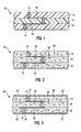
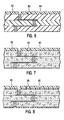
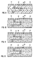
- a surface layer is shown in Figure 6 as surface layer 80 having waveguides 82 (e.g., an optical fiber) and/or 84 (e.g., an open channel).
- the composition of the surface layer 80 is 30 to 100% by weight polymeric material and 70 to 0% by weight ceramic.
- the polymeric material should be an optically transparent, low (optical) loss material.
- Some exemplary materials for the surface layer are fluorinated polymers such as fluorinated and perfluorinated polyimides; acrylic polymers such as fluoroalkyl (methacrylate), perfluoro(methacrylate), and alkylmethacrylate homopolymers/copolymers such as PMMA and PMMA/polystyrene copolymers; polyetherketone; polyesters; and urethane-acrylic polymers.
- the waveguides can be optical fibers, open channels for optical transmission or optical waveguides.
- the dielectric material should preferably have a different index of refraction so as to refract the light and keep it within the waveguide.
- a second embodiment according to this invention comprises metal conductors and a partially densified ceramic matrix which has been surface sealed or bulk filled with an organic or an organometallic polymer insulator having low dielectric constant, low CTE, and low moisture absorption.
- Fabrication of this structure can be obtained by using a multilayer-ceramic (MLC) type process involving preparation of a green sheet slurry comprising ceramic filler and a polymer binder system in a solvent vehicle, sheet casting on a carrier and solvent volatilization to form green sheets. After a drying operation to remove the solvent, and blanking operation, the individual layers are patterned for via definition by mechanical punching, laser drilling, mechanical drilling, e-beam machining, or chemically etching.
- MLC multilayer-ceramic
- Subsequent steps after via punching involve personalization employing a screen-on metal paste, drying, inspection of individual screened sheets, stacking and alignment, lamination, binder burn-off, densification of metal and partial sintering of the ceramic by subjecting it to an elevated temperature to produce a bisque fired "necked" rigid skeletal network or porous ceramic body.
- the structure is then treated with an organic or organometallic polymer solution or solvent-free polymerizable reactive monomer/oligomer composition such that it either forms a surface skin-like seal or fills the bulk matrix porosity.
- Subsequent thermal treatment to remove solvent and curing or polymerization provides a polymer encapsulated structure.
- Subsequent processing involves deposition of pad metallurgy, electrical test, semiconductor device joining, module electrical test and PCB connections.
- Proportion of the polymer filler relative to the metallized ceramic composite body will depend on the level of porosity in ceramic, the filling of bulk porosity or only the surface region and encapsulation, and the density of metal pattern.
- Preferred polymers for forming the green sheet slurry for the polymer-filled ceramic structure are those which essentially completely depolymerize to monomeric or thermally decompose to monomeric/oligomeric species which volatilize when conventionally heated in a binder burn-off heating cycle to 300-400 °C.
- polymers suitable for this purpose include a poly(alkyl methacrylate), preferably, PMMA [poly(methyl methacrylate)], PMMA-poly-n-butyl methacrylate copolymers, poly(t-butyl methacrylate), P ⁇ MS [poly( ⁇ -methyl styrene)], polyvinyl butyral, poly(propylene oxide), and PIB [poly( isobutylene)], PMMA-PIB blends, which readily depolymerizes at temperature less than 400°C.
- PMMA poly(methyl methacrylate)
- PMMA-poly-n-butyl methacrylate copolymers poly(t-butyl methacrylate)
- P ⁇ MS poly( ⁇ -methyl styrene)
- polyvinyl butyral poly(propylene oxide)
- PIB poly( isobutylene)
- the electrically conductive metal paste for via fill may comprise a metal powder such as Au, Au-Cu, Au-Sn, Cu-Sn intermetallics, Ag plated Cu, or Au plated Ni, and optionally an inorganic particulate such a glass frit, in a polymer binder system which is readily removable by heating at less than 350-450 °C.
- the mixture is milled in a roll mill to form an homogeneous paste.
- the structure is treated with a solvent-less or solvent carrying polymer or pre-polymer solution, preferably a solvent-less reactive oligomer composition, to flow in between the porous region in the ceramic network.
- a solvent-less or solvent carrying polymer or pre-polymer solution preferably a solvent-less reactive oligomer composition
- BCB resin solution or divinyl siloxane-bis-benzocyclobutene (DVS-BCB) prepolymer solution (CYCLOTENE resins, Dow Chemical Co.) is dispensed over the substrate in multiple applications, heated at 100-150 °C in-between applications to slowly remove solvent or low molecular weight species after each application, and a final cure to 350 °C in a programmed oven or furnace to form a thermally stable, solvent resistant polymer matrix encapsulating the ceramic bulk porosity.
- the BCB polymers are available as partially polymerized (B-staged) resins in solvent.
- the cured crosslinked polymers have several advantages, particularly, low dielectric constant (2.65 at 1KHz to 1MHz) and dielectric loss tangent ( ⁇ 0.0008 at 1KHz), resistance to solvents when fully crosslinked, and high thermal stability, and low moisture absorption.
- Other low viscosity materials can also be used for back filling the ceramic porosity, for example, SILK polymers, polyarylene ether, low molecular weight cross linkable polyorganosilanes, such as poly(methylsilsesquioxane) which can be obtained in solution with high solids, can be dispensed similar to the BCB solution, and baked to temperatures up to 400 °C to form a crosslinked insulating matrix in ceramic skeletal network.
- thermosetting polymeric systems that can be used for post-sinter surface seal or bulk impregnation into the necked-ceramic bulk include acetylene terminated polyimides such as Thermid-Isoimide series of materials, for example, IP-610 or 615 oligomers; low CTE polyimides, e.g., BPDA-PDA, BPDA-ODA; bis-maleimide-triazine resins (BT-resin), cyanate ester-epoxy blends, poly(amic ethyl ester) such as PMDA-ODA amic-ethyl ester, BPDA-PDA amic-ethyl ester, and related materials.
- acetylene terminated polyimides such as Thermid-Isoimide series of materials, for example, IP-610 or 615 oligomers
- low CTE polyimides e.g., BPDA-PDA, BPDA-ODA
- Ceramic material is mixed with a polymer binder material in a solvent carrier with appropriate additives such as a plasticizer, surfactant/dispersant, antioxidant and coloring agents to form dispersion 63, also known as a green sheet slurry.
- a plasticizer such as a plasticizer, surfactant/dispersant, antioxidant and coloring agents
- dispersion 63 also known as a green sheet slurry.
- the aforementioned ingredients are mixed in a high shear mixing process using a planetary mixer or a ball mill or a roll mill to provide an homogeneous slurry for casting.
- coupling agents such as organosilanes or organotitanates
- a particle surface modifying agent can be mixed in with the organic binder system and then the ceramic material is blended in to form the composite slurry.
- the polymer binder is chosen so as to depolymerize as mentioned earlier.
- the composite slurry thus formed is cast into sheets (called green sheets) on a carrier, typically PET, polyethylene or polypropylene, using a sheet casting process (64 in Figure 5). After a drying operation to remove solvent in the cast sheets, a blanking operation generates the desired size individual layers of the composite substrate and punches registration holes necessary for alignment.
- a carrier typically PET, polyethylene or polypropylene
- the individual layers are inspected and then the desired number of layers are aligned and stacked (72 in Figure 4), placing a thin non-stick polymer sheet on the top and bottom layers of the stack, and laminated using a hydraulic uniaxial press at 150-350°C and 200-2000 psi pressure to form a multilayer composite interconnect structure.
- At least one surface layer can be added that is especially adapted for supporting high density electronic metal conductors and/or high density optical waveguides for the transmission of electrons and/or photons, respectively.
- a surface layer is shown in Figures 7 and 8 as surface layer 86 having waveguides 88 (e.g., an optical fiber) and/or 90 (e.g., an open channel).
- Figure 7 generally corresponds to Figure 2 but with the surface layer 86.
- Figure 8 generally corresponds to Figure 3 but with the surface layer 86.
- the composition of the surface layers is 30 to 100% by weight polymeric material and 70 to 0% by weight ceramic.
- ceramic-filled polymeric layer 98 can be formed to support waveguide 88 and/or channel 90 as shown in Figures 10 and 11.
- channel 90 should be lined with a layer 100 of polymeric material. Note that channel 90 is left unfilled.
- polymeric surface layer 102 is formed.
- the polymeric material should be an optically transparent, low (optical) loss material.
- Some exemplary materials for the surface layer are fluorinated polymers such as fluorinated and perfluorinated polyimides; acrylic polymers such as fluoroalkyl (methacrylate), perfluoro(methacrylate), and alkylmethacrylate homopolymers/copolymers such as PMMA and PMMA/polystyrene copolymers; polyetherketone; polyesters; and urethane-acrylic polymers.
- the waveguides can be optical fibers, open channels for optical transmission or opotical waveguides.
- the dielectric material should preferably have a different index of refraction so as to refract the light and keep it within the waveguide.
Landscapes
- Engineering & Computer Science (AREA)
- Microelectronics & Electronic Packaging (AREA)
- Chemical & Material Sciences (AREA)
- Ceramic Engineering (AREA)
- Inorganic Chemistry (AREA)
- Laminated Bodies (AREA)
- Optical Integrated Circuits (AREA)
- Production Of Multi-Layered Print Wiring Board (AREA)
- Compositions Of Macromolecular Compounds (AREA)
- Manufacture Of Macromolecular Shaped Articles (AREA)
- Addition Polymer Or Copolymer, Post-Treatments, Or Chemical Modifications (AREA)
Applications Claiming Priority (2)
| Application Number | Priority Date | Filing Date | Title |
|---|---|---|---|
| US09/606,359 US6528145B1 (en) | 2000-06-29 | 2000-06-29 | Polymer and ceramic composite electronic substrates |
| US606359 | 2000-06-29 |
Publications (2)
| Publication Number | Publication Date |
|---|---|
| EP1168436A2 true EP1168436A2 (fr) | 2002-01-02 |
| EP1168436A3 EP1168436A3 (fr) | 2008-11-19 |
Family
ID=24427650
Family Applications (1)
| Application Number | Title | Priority Date | Filing Date |
|---|---|---|---|
| EP01305287A Withdrawn EP1168436A3 (fr) | 2000-06-29 | 2001-06-18 | Substrat composite electronique polymerique et ceramique |
Country Status (7)
| Country | Link |
|---|---|
| US (1) | US6528145B1 (fr) |
| EP (1) | EP1168436A3 (fr) |
| JP (1) | JP3745653B2 (fr) |
| KR (1) | KR100462451B1 (fr) |
| CN (1) | CN1170314C (fr) |
| MY (1) | MY117336A (fr) |
| TW (1) | TW515055B (fr) |
Cited By (8)
| Publication number | Priority date | Publication date | Assignee | Title |
|---|---|---|---|---|
| CN1297000C (zh) * | 2002-08-14 | 2007-01-24 | 国际商业机器公司 | 包含应力调节覆盖层的互连结构及其制造方法 |
| WO2007146383A1 (fr) * | 2006-06-15 | 2007-12-21 | E. I. Du Pont De Nemours And Company | Compositions encapsulantes organiques à base de polymères hétérocycliques pour la protection de composants électroniques |
| WO2011063247A3 (fr) * | 2009-11-20 | 2011-09-29 | E. I. Du Pont De Nemours And Company | Films intercalaires servant à des applications d'emballage de semi-conducteurs, et procédés associés |
| CN102550136A (zh) * | 2009-09-15 | 2012-07-04 | 罗伯特·博世有限公司 | 用于生产陶瓷器件的方法、陶瓷器件与器件布置 |
| EP2712027A4 (fr) * | 2011-04-28 | 2015-04-22 | Kuang Chi Innovative Tech Ltd | Substrat diélectrique en métamatériau, et procédé de traitement associé |
| US20230317592A1 (en) * | 2022-04-01 | 2023-10-05 | Intel Corporation | Substrate with low-permittivity core and buildup layers |
| WO2025160248A1 (fr) * | 2024-01-25 | 2025-07-31 | Yield Engineering Systems, Inc. | Revêtements diélectriques sur des trous d'interconnexion traversant le verre |
| US12543536B2 (en) | 2023-11-27 | 2026-02-03 | Toto Ltd. | Electrostatic chuck |
Families Citing this family (126)
| Publication number | Priority date | Publication date | Assignee | Title |
|---|---|---|---|---|
| WO2000018202A1 (fr) * | 1998-09-17 | 2000-03-30 | Ibiden Co., Ltd. | Tableau de connexions multicouche d'accumulation |
| US6875719B2 (en) * | 2000-04-27 | 2005-04-05 | Industrial Technology Research Institute | Catalyst composition for preparing olefin polymers |
| JP4095763B2 (ja) * | 2000-09-06 | 2008-06-04 | 株式会社ルネサステクノロジ | 半導体装置及びその製造方法 |
| US6800815B1 (en) | 2001-01-16 | 2004-10-05 | National Semiconductor Corporation | Materials and structure for a high reliability bga connection between LTCC and PB boards |
| US6656313B2 (en) * | 2001-06-11 | 2003-12-02 | International Business Machines Corporation | Structure and method for improved adhesion between two polymer films |
| US6682619B2 (en) * | 2001-07-17 | 2004-01-27 | Sikorsky Aircraft Corporation | Composite pre-preg ply having tailored dielectrical properties and method of fabrication thereof |
| US20030137815A1 (en) * | 2002-01-18 | 2003-07-24 | Matsushita Electric Industrial Co., Ltd. | Printed wiring board and method of manufacturing the same |
| US7714432B2 (en) * | 2002-07-26 | 2010-05-11 | Intel Corporation | Ceramic/organic hybrid substrate |
| KR100483622B1 (ko) * | 2002-08-16 | 2005-04-19 | 삼성전기주식회사 | 광도파로 소자를 인쇄회로기판에 부착하는 방법 |
| JP2005539382A (ja) * | 2002-09-16 | 2005-12-22 | ワールド・プロパティーズ・インコーポレイテッド | 液晶ポリマ複合物、その製造方法、およびそれから形成された物品 |
| JP4426805B2 (ja) * | 2002-11-11 | 2010-03-03 | 日本特殊陶業株式会社 | 配線基板およびその製造方法 |
| TWI234210B (en) * | 2002-12-03 | 2005-06-11 | Sanyo Electric Co | Semiconductor module and manufacturing method thereof as well as wiring member of thin sheet |
| KR100451635B1 (ko) * | 2002-12-10 | 2004-10-08 | 삼성전기주식회사 | 섬유 블록과 파이프 블록, 및 이를 이용하여 다층인쇄회로기판의 층간 광신호를 연결하는 방법 |
| EP1586592B1 (fr) * | 2002-12-25 | 2010-04-21 | Daikin Industries, Ltd. | Fluoropolymeres et compositions les comprenant |
| DE10302104A1 (de) * | 2003-01-21 | 2004-08-05 | Friwo Gerätebau Gmbh | Verfahren zum Herstellen von Schaltungsträgern mit intergrierten passiven Bauelementen |
| US6764748B1 (en) * | 2003-03-18 | 2004-07-20 | International Business Machines Corporation | Z-interconnections with liquid crystal polymer dielectric films |
| US7265300B2 (en) * | 2003-03-21 | 2007-09-04 | Commscope Solutions Properties, Llc | Next high frequency improvement using hybrid substrates of two materials with different dielectric constant frequency slopes |
| TW573444B (en) * | 2003-04-22 | 2004-01-21 | Ind Tech Res Inst | Substrate having organic and inorganic functional package |
| US7126228B2 (en) * | 2003-04-23 | 2006-10-24 | Micron Technology, Inc. | Apparatus for processing semiconductor devices in a singulated form |
| KR20040106674A (ko) * | 2003-06-11 | 2004-12-18 | 삼성전자주식회사 | 광도파로 적층 인쇄회로기판 및 광연결 블록의 구조와 그광도파로층 제작 방법 |
| US7164197B2 (en) * | 2003-06-19 | 2007-01-16 | 3M Innovative Properties Company | Dielectric composite material |
| US7226654B2 (en) * | 2003-07-29 | 2007-06-05 | Kyocera Corporation | Laminated wiring board and its mounting structure |
| US7129318B2 (en) * | 2003-09-02 | 2006-10-31 | I.S.T. (Ma) Corporation | RTM and RI processable polyimide resins |
| JP2005195690A (ja) * | 2003-12-26 | 2005-07-21 | Toshiba Corp | 金属含有樹脂粒子、樹脂粒子、及び電子回路の製造方法 |
| US7015075B2 (en) * | 2004-02-09 | 2006-03-21 | Freescale Semiconuctor, Inc. | Die encapsulation using a porous carrier |
| US7342181B2 (en) * | 2004-03-12 | 2008-03-11 | Commscope Inc. Of North Carolina | Maximizing capacitance per unit area while minimizing signal transmission delay in PCB |
| US7429789B2 (en) * | 2004-03-31 | 2008-09-30 | Endicott Interconnect Technologies, Inc. | Fluoropolymer dielectric composition for use in circuitized substrates and circuitized substrate including same |
| US7470990B2 (en) * | 2004-03-31 | 2008-12-30 | Endicott Interconnect Technologies, Inc. | Low moisture absorptive circuitized substrate with reduced thermal expansion, method of making same, electrical assembly utilizing same, and information handling system utilizing same |
| US7190594B2 (en) | 2004-05-14 | 2007-03-13 | Commscope Solutions Properties, Llc | Next high frequency improvement by using frequency dependent effective capacitance |
| US7980900B2 (en) * | 2004-05-14 | 2011-07-19 | Commscope, Inc. Of North Carolina | Next high frequency improvement by using frequency dependent effective capacitance |
| US8221885B2 (en) | 2004-06-02 | 2012-07-17 | Cool Options, Inc. a corporation of the State of New Hampshire | Thermally conductive polymer compositions having low thermal expansion characteristics |
| US20060001145A1 (en) * | 2004-07-03 | 2006-01-05 | Aptos Corporation | Wafer level mounting frame with passive components integration for ball grid array packaging |
| WO2006014582A2 (fr) * | 2004-07-08 | 2006-02-09 | Dow Corning Corporation | Interconnexion optique courte portee |
| DE102004037381A1 (de) * | 2004-08-02 | 2006-03-16 | Patent-Treuhand-Gesellschaft für elektrische Glühlampen mbH | Kittlos gesockelte Lampe |
| CN101014890B (zh) | 2004-09-08 | 2011-01-19 | 东丽株式会社 | 光布线用树脂组合物和光电复合布线基板 |
| KR100638620B1 (ko) * | 2004-09-23 | 2006-10-26 | 삼성전기주식회사 | 임베디드 수동소자용 인쇄회로기판재료 |
| TW200613447A (en) * | 2004-10-28 | 2006-05-01 | Ind Tech Res Inst | Dielectric constant adjustable resin composition, prepreg and copper clad laminate utilizing the same |
| JP2006128520A (ja) * | 2004-10-29 | 2006-05-18 | Tdk Corp | 多層基板の製造方法 |
| JP2006128519A (ja) * | 2004-10-29 | 2006-05-18 | Tdk Corp | 多層基板の製造方法 |
| JP2006152173A (ja) * | 2004-11-30 | 2006-06-15 | Sumitomo Bakelite Co Ltd | 樹脂組成物、樹脂層、樹脂層付きキャリア材料および回路基板 |
| WO2006074550A1 (fr) * | 2005-01-14 | 2006-07-20 | National Research Council Of Canada | Implant osseux prothetique et biomimetique |
| US7352061B2 (en) * | 2005-05-20 | 2008-04-01 | Intel Corporation | Flexible core for enhancement of package interconnect reliability |
| US7095602B1 (en) * | 2005-06-29 | 2006-08-22 | Murata Manufacturing Co., Ltd. | Ceramic structure and nonreciprocal circuit device |
| US7342183B2 (en) * | 2005-07-11 | 2008-03-11 | Endicott Interconnect Technologies, Inc. | Circuitized substrate with sintered paste connections, multilayered substrate assembly, electrical assembly and information handling system utilizing same |
| EP1909322A4 (fr) * | 2005-07-27 | 2011-08-03 | Murata Manufacturing Co | Composant électronique superposé, dispositif électronique et procédé de fabrication de composant électronique superposé |
| JP2007096185A (ja) * | 2005-09-30 | 2007-04-12 | Sanyo Electric Co Ltd | 回路基板 |
| JP5309316B2 (ja) * | 2006-02-06 | 2013-10-09 | 国立大学法人東北大学 | チップ素子 |
| US20070235450A1 (en) * | 2006-03-30 | 2007-10-11 | Advanced Composite Materials Corporation | Composite materials and devices comprising single crystal silicon carbide heated by electromagnetic radiation |
| JP4862893B2 (ja) * | 2006-06-02 | 2012-01-25 | 株式会社村田製作所 | 多層セラミック電子部品およびその製造方法 |
| US7407415B2 (en) * | 2006-06-07 | 2008-08-05 | International Business Machines Corporation | Crosstalk reduction in dual inline memory module (DIMM) connectors |
| KR100752019B1 (ko) * | 2006-09-29 | 2007-08-28 | 삼성전기주식회사 | 인쇄회로기판용 절연재 |
| JP5175476B2 (ja) * | 2007-02-28 | 2013-04-03 | 三洋電機株式会社 | 回路装置の製造方法 |
| US20080217748A1 (en) * | 2007-03-08 | 2008-09-11 | International Business Machines Corporation | Low cost and low coefficient of thermal expansion packaging structures and processes |
| GB0706638D0 (en) * | 2007-04-04 | 2007-05-16 | Mbda Uk Ltd | A high-dielectric material |
| US20120052222A1 (en) * | 2007-08-10 | 2012-03-01 | Gagne Robert R | Lightweight ballistic protection materials, |
| WO2009045932A1 (fr) | 2007-09-28 | 2009-04-09 | Tri-Star Laminates, Inc. | Meilleurs systèmes et procédés de perçage de trous dans des cartes à circuit imprimé |
| JP2009098654A (ja) * | 2007-09-28 | 2009-05-07 | Dainippon Printing Co Ltd | 光学積層体、偏光板及び画像表示装置 |
| US20100283570A1 (en) * | 2007-11-14 | 2010-11-11 | Lavoie Adrien R | Nano-encapsulated magnetic particle composite layers for integrated silicon voltage regulators |
| US20100012354A1 (en) * | 2008-07-14 | 2010-01-21 | Logan Brook Hedin | Thermally conductive polymer based printed circuit board |
| WO2010009381A1 (fr) * | 2008-07-18 | 2010-01-21 | World Properties, Inc. | Matériaux de circuit, stratifiés de circuit, et procédé de fabrication de ceux-ci |
| KR100983219B1 (ko) * | 2008-12-05 | 2010-09-20 | 조근호 | 직접인쇄방식에 의한 인쇄회로기판의 제조방법 및 이에 의하여 제조된 인쇄회로기판 |
| US8047879B2 (en) * | 2009-01-26 | 2011-11-01 | Commscope, Inc. Of North Carolina | Printed wiring boards and communication connectors having series inductor-capacitor crosstalk compensation circuits that share a common inductor |
| TW201032689A (en) * | 2009-02-20 | 2010-09-01 | Unimicron Technology Corp | Composite circuit substrate structure |
| DE102009024982B4 (de) * | 2009-06-16 | 2013-01-10 | Solarworld Innovations Gmbh | Maskierungsverfahren, Verwendung des Verfahrens und Zwischenprodukt und Verfahren zur Herstellung einer Kontakt-Struktur für ein Halbleiter-Bauelement |
| KR20110019536A (ko) * | 2009-08-20 | 2011-02-28 | 삼성전기주식회사 | 세라믹 기판 및 그 제조방법 |
| KR101123900B1 (ko) * | 2009-08-28 | 2012-03-23 | 한국세라믹기술원 | 복합 소재 및 그 제조 방법 |
| CN102117670B (zh) * | 2009-10-29 | 2016-05-04 | 住友金属矿山株式会社 | 电阻体材料、电阻薄膜形成用溅射靶、电阻薄膜、薄膜电阻器以及它们的制造方法 |
| JP4929423B2 (ja) | 2010-07-22 | 2012-05-09 | 日本碍子株式会社 | 成形体、及び、成形体の製造方法 |
| US20120286416A1 (en) * | 2011-05-11 | 2012-11-15 | Tessera Research Llc | Semiconductor chip package assembly and method for making same |
| EP2737275A4 (fr) | 2011-07-28 | 2014-09-17 | Mac Llc | Géométrie de corps de munition en polymère |
| US9182204B2 (en) | 2011-07-28 | 2015-11-10 | Mac, Llc | Subsonic ammunition casing |
| DE102011080299B4 (de) * | 2011-08-02 | 2016-02-11 | Infineon Technologies Ag | Verfahren, mit dem ein Schaltungsträger hergestellt wird, und Verfahren zur Herstellung einer Halbleiteranordnung |
| WO2013042749A1 (fr) * | 2011-09-22 | 2013-03-28 | 日立化成株式会社 | Corps stratifié, carte stratifiée, carte stratifiée multicouche, carte imprimée et procédé de production de carte stratifiée |
| JPWO2013042751A1 (ja) * | 2011-09-22 | 2015-03-26 | 日立化成株式会社 | 積層体、積層板、多層積層板、プリント配線板及び積層板の製造方法 |
| US9101061B2 (en) * | 2011-09-22 | 2015-08-04 | Hitachi Chemical Company, Ltd. | Laminate body, laminate plate, multilayer laminate plate, printed wiring board, and method for manufacture of laminate plate |
| US10543662B2 (en) | 2012-02-08 | 2020-01-28 | Corning Incorporated | Device modified substrate article and methods for making |
| FR2988223B1 (fr) * | 2012-03-19 | 2016-09-02 | Solarwell | Dispositif emettant de la lumiere contenant des nanocristaux colloidaux semiconducteurs anisotropes aplatis et procede de fabrication de tels dispositifs |
| RU2639315C2 (ru) * | 2012-07-12 | 2017-12-21 | ЛЭЙБИНЕЛ, ЭлЭлСи | Компоновка шин нагрузки и способ ее производства |
| TWI617437B (zh) | 2012-12-13 | 2018-03-11 | 康寧公司 | 促進控制薄片與載體間接合之處理 |
| US10086584B2 (en) | 2012-12-13 | 2018-10-02 | Corning Incorporated | Glass articles and methods for controlled bonding of glass sheets with carriers |
| US9340443B2 (en) | 2012-12-13 | 2016-05-17 | Corning Incorporated | Bulk annealing of glass sheets |
| TW201429708A (zh) * | 2012-12-13 | 2014-08-01 | Corning Inc | 玻璃及製造玻璃物品的方法 |
| US10014177B2 (en) | 2012-12-13 | 2018-07-03 | Corning Incorporated | Methods for processing electronic devices |
| JP6377074B2 (ja) * | 2012-12-20 | 2018-08-22 | ダウ グローバル テクノロジーズ エルエルシー | 無線通信塔のためのポリマー複合体構成部品 |
| KR20140091346A (ko) * | 2013-01-11 | 2014-07-21 | 삼성디스플레이 주식회사 | 표시 장치 및 그 제조 방법 |
| US10510576B2 (en) | 2013-10-14 | 2019-12-17 | Corning Incorporated | Carrier-bonding methods and articles for semiconductor and interposer processing |
| AT515069B1 (de) * | 2013-11-07 | 2019-10-15 | At & S Austria Tech & Systemtechnik Ag | Leiterplattenstruktur |
| ES2728242T3 (es) | 2014-01-13 | 2019-10-23 | Mac Llc | Vaina de munición polimérica |
| WO2015112958A1 (fr) | 2014-01-27 | 2015-07-30 | Corning Incorporated | Articles et procédés pour la liaison contrôlée de feuilles minces avec des supports |
| US9453714B2 (en) | 2014-04-04 | 2016-09-27 | Mac, Llc | Method for producing subsonic ammunition casing |
| CN106457758B (zh) | 2014-04-09 | 2018-11-16 | 康宁股份有限公司 | 装置改性的基材制品及其制备方法 |
| US9379298B2 (en) * | 2014-10-03 | 2016-06-28 | Henkel IP & Holding GmbH | Laminate sub-mounts for LED surface mount package |
| CN107635769B (zh) | 2015-05-19 | 2020-09-15 | 康宁股份有限公司 | 使片材与载体粘结的制品和方法 |
| JP7106276B2 (ja) | 2015-06-26 | 2022-07-26 | コーニング インコーポレイテッド | シート及び担体を有する物品及び方法 |
| US10008382B2 (en) | 2015-07-30 | 2018-06-26 | Taiwan Semiconductor Manufacturing Company, Ltd. | Semiconductor device having a porous low-k structure |
| KR20170025021A (ko) * | 2015-08-27 | 2017-03-08 | 삼성전기주식회사 | 인쇄회로기판 제조용 수지 부착 동박 및 이를 이용한 인쇄회로기판의 제조방법 |
| WO2017069752A1 (fr) * | 2015-10-21 | 2017-04-27 | Hewlett-Packard Development Company, L.P. | Impression en trois dimensions (3d) |
| US11367959B2 (en) | 2015-10-28 | 2022-06-21 | Rogers Corporation | Broadband multiple layer dielectric resonator antenna and method of making the same |
| US10476164B2 (en) | 2015-10-28 | 2019-11-12 | Rogers Corporation | Broadband multiple layer dielectric resonator antenna and method of making the same |
| US10374315B2 (en) | 2015-10-28 | 2019-08-06 | Rogers Corporation | Broadband multiple layer dielectric resonator antenna and method of making the same |
| US20170287838A1 (en) | 2016-04-02 | 2017-10-05 | Intel Corporation | Electrical interconnect bridge |
| WO2018022447A1 (fr) * | 2016-07-27 | 2018-02-01 | Corning Incorporated | Composite de céramique et de polymère, ses procédés de fabrication et ses utilisations |
| TW202216444A (zh) | 2016-08-30 | 2022-05-01 | 美商康寧公司 | 用於片材接合的矽氧烷電漿聚合物 |
| TWI810161B (zh) | 2016-08-31 | 2023-08-01 | 美商康寧公司 | 具以可控制式黏結的薄片之製品及製作其之方法 |
| KR20190097141A (ko) * | 2016-12-16 | 2019-08-20 | 사빅 글로벌 테크놀러지스 비.브이. | 천연 재료 및 냉간 소결에 의해 만들어진 구조화된 세라믹 복합체 |
| CN106876357B (zh) * | 2017-01-24 | 2024-11-15 | 深圳市槟城电子股份有限公司 | 用于芯片封装的电极以及使用该电极的芯片封装结构 |
| CN106604536B (zh) * | 2017-01-26 | 2019-05-21 | 上海安缔诺科技有限公司 | 聚四氟乙烯复合微波介质材料及其制备方法 |
| US11075130B2 (en) | 2017-03-30 | 2021-07-27 | Intel Corporation | Package substrate having polymer-derived ceramic core |
| US11876295B2 (en) | 2017-05-02 | 2024-01-16 | Rogers Corporation | Electromagnetic reflector for use in a dielectric resonator antenna system |
| US11283189B2 (en) * | 2017-05-02 | 2022-03-22 | Rogers Corporation | Connected dielectric resonator antenna array and method of making the same |
| KR102312067B1 (ko) | 2017-06-07 | 2021-10-13 | 로저스코포레이션 | 유전체 공진기 안테나 시스템 |
| JP7260523B2 (ja) | 2017-08-18 | 2023-04-18 | コーニング インコーポレイテッド | ポリカチオン性高分子を使用した一時的結合 |
| US11331692B2 (en) | 2017-12-15 | 2022-05-17 | Corning Incorporated | Methods for treating a substrate and method for making articles comprising bonded sheets |
| US11616302B2 (en) | 2018-01-15 | 2023-03-28 | Rogers Corporation | Dielectric resonator antenna having first and second dielectric portions |
| US10892544B2 (en) | 2018-01-15 | 2021-01-12 | Rogers Corporation | Dielectric resonator antenna having first and second dielectric portions |
| US10910722B2 (en) | 2018-01-15 | 2021-02-02 | Rogers Corporation | Dielectric resonator antenna having first and second dielectric portions |
| RU2715085C2 (ru) * | 2018-07-02 | 2020-02-25 | Виталий Евгеньевич Поляков | Активная среда для волоконных лазеров и способ ее изготовления |
| US11426818B2 (en) | 2018-08-10 | 2022-08-30 | The Research Foundation for the State University | Additive manufacturing processes and additively manufactured products |
| US11031697B2 (en) | 2018-11-29 | 2021-06-08 | Rogers Corporation | Electromagnetic device |
| CN113169455A (zh) | 2018-12-04 | 2021-07-23 | 罗杰斯公司 | 电介质电磁结构及其制造方法 |
| KR20200080992A (ko) | 2018-12-27 | 2020-07-07 | 삼성전자주식회사 | 복합체, 성형품, 전지 케이스, 및 전지 |
| US11482790B2 (en) | 2020-04-08 | 2022-10-25 | Rogers Corporation | Dielectric lens and electromagnetic device with same |
| CN111534820B (zh) * | 2020-06-15 | 2021-03-23 | 北京师范大学 | 一种自支撑绝缘介质及其制备方法和应用 |
| CN115508919A (zh) * | 2021-06-22 | 2022-12-23 | 瑞仪光电(南京)有限公司 | 光学膜片、背光模组、显示装置及光学膜片的制造方法 |
| CN114911003B (zh) * | 2022-05-31 | 2023-09-22 | 上海大学 | 一种基于包层紫外光刻的光波导制备方法 |
| US20240222211A1 (en) * | 2022-12-29 | 2024-07-04 | Intel Corporation | Ic die packages with low cte dielectric materials |
Family Cites Families (38)
| Publication number | Priority date | Publication date | Assignee | Title |
|---|---|---|---|---|
| US4680220A (en) * | 1985-02-26 | 1987-07-14 | W. L. Gore & Associates, Inc. | Dielectric materials |
| EP0196865B1 (fr) * | 1985-03-27 | 1990-09-12 | Ibiden Co, Ltd. | Substrats pour circuits électroniques |
| JPH0634435B2 (ja) * | 1985-11-27 | 1994-05-02 | イビデン株式会社 | 電子回路用多層基板 |
| US4810563A (en) * | 1986-03-14 | 1989-03-07 | The Bergquist Company | Thermally conductive, electrically insulative laminate |
| US5384181B1 (en) | 1987-02-17 | 2000-06-13 | World Properties Inc | Low volume fraction ceramic filled fluoropolymeric composite material |
| US5061548A (en) | 1987-02-17 | 1991-10-29 | Rogers Corporation | Ceramic filled fluoropolymeric composite material |
| US4849284A (en) * | 1987-02-17 | 1989-07-18 | Rogers Corporation | Electrical substrate material |
| EP0309982A3 (fr) * | 1987-09-30 | 1990-09-12 | E.I. Du Pont De Nemours And Company | Plaques composite polymère-céramique |
| US5139852A (en) * | 1988-03-11 | 1992-08-18 | International Business Machines Corporation | Low dielectric composite substrate |
| JPH02148789A (ja) * | 1988-03-11 | 1990-06-07 | Internatl Business Mach Corp <Ibm> | 電子回路基板 |
| JPH0811781B2 (ja) * | 1988-03-26 | 1996-02-07 | 松下電工株式会社 | 賦形高誘電性ポリフェニレンオキサイド系樹脂組成物 |
| JPH088416B2 (ja) * | 1988-10-25 | 1996-01-29 | 日本電気株式会社 | セラミック多層回路基板の製造方法 |
| JPH03177376A (ja) * | 1989-12-04 | 1991-08-01 | Japan Gore Tex Inc | セラミック基板 |
| US5213878A (en) * | 1990-03-23 | 1993-05-25 | Minnesota Mining And Manufacturing Company | Ceramic composite for electronic applications |
| JPH0491497A (ja) * | 1990-08-02 | 1992-03-24 | Sumitomo Chem Co Ltd | セラミック―樹脂複合体よりなる配線板の製造方法 |
| JPH04103349A (ja) * | 1990-08-23 | 1992-04-06 | Hitachi Chem Co Ltd | 熱可塑性樹脂金属張積層板の製造方法 |
| US5541249A (en) | 1990-12-18 | 1996-07-30 | Hoechst Celanese Corp. | Injection moldable ceramic and metallic compositions and method of preparing the same |
| US5287619A (en) | 1992-03-09 | 1994-02-22 | Rogers Corporation | Method of manufacture multichip module substrate |
| JP3287871B2 (ja) * | 1992-04-01 | 2002-06-04 | ソニー株式会社 | プリント基板の製造方法 |
| JPH05291706A (ja) * | 1992-04-13 | 1993-11-05 | Mitsubishi Gas Chem Co Inc | プリント配線用基板の製造法 |
| JPH06219819A (ja) * | 1993-01-20 | 1994-08-09 | Asahi Glass Co Ltd | セラミックスグリーンシート及びセラミックス基板 |
| JPH06281831A (ja) * | 1993-03-25 | 1994-10-07 | Nippon Telegr & Teleph Corp <Ntt> | 電気配線・光配線混載フレキシブルプリント配線板及びその基板 |
| US5358775A (en) | 1993-07-29 | 1994-10-25 | Rogers Corporation | Fluoropolymeric electrical substrate material exhibiting low thermal coefficient of dielectric constant |
| JP3442895B2 (ja) * | 1994-07-04 | 2003-09-02 | 新光電気工業株式会社 | 基板製造用焼成体、基板およびその製造方法 |
| DE69417027T2 (de) * | 1994-08-02 | 2000-01-05 | Mitsubishi Gas Chemical Co., Inc. | Verfahren zur Produktion einer Rohplatte für gedruckte Leiterplatten |
| US5571609A (en) | 1994-10-13 | 1996-11-05 | Rogers Corporation | Polybutadiene and polyisoprene based thermosetting compositions and method of manufacture thereof |
| JPH08125339A (ja) * | 1994-10-21 | 1996-05-17 | Kyocera Corp | 多層配線基板の製造方法 |
| JP3199584B2 (ja) * | 1994-10-31 | 2001-08-20 | 京セラ株式会社 | 多層配線基板 |
| US5552210A (en) * | 1994-11-07 | 1996-09-03 | Rogers Corporation | Ceramic filled composite polymeric electrical substrate material exhibiting high dielectric constant and low thermal coefficient of dielectric constant |
| JPH08186376A (ja) * | 1994-12-28 | 1996-07-16 | Hitachi Ltd | 高密度薄膜多層配線基板並びにその実装構造体及びその製造方法 |
| JPH08231274A (ja) * | 1995-02-24 | 1996-09-10 | Kyocera Corp | 樹脂−セラミックス複合材及びこれを用いた電子回路基板 |
| US5670262A (en) * | 1995-05-09 | 1997-09-23 | The Dow Chemical Company | Printing wiring board(s) having polyimidebenzoxazole dielectric layer(s) and the manufacture thereof |
| US5919546A (en) * | 1995-06-22 | 1999-07-06 | Shinko Electric Industries Co. Ltd. | Porous ceramic impregnated wiring body |
| JPH10100320A (ja) * | 1996-09-30 | 1998-04-21 | Mitsubishi Gas Chem Co Inc | 複合セラミックス板およびその製造法 |
| US5965273A (en) * | 1997-01-31 | 1999-10-12 | Hoechst Celanese Corporation | Polymeric compositions having a temperature-stable dielectric constant |
| US5922453A (en) * | 1997-02-06 | 1999-07-13 | Rogers Corporation | Ceramic-filled fluoropolymer composite containing polymeric powder for high frequency circuit substrates |
| US6845184B1 (en) * | 1998-10-09 | 2005-01-18 | Fujitsu Limited | Multi-layer opto-electronic substrates with electrical and optical interconnections and methods for making |
| US6233817B1 (en) * | 1999-01-17 | 2001-05-22 | Delphi Technologies, Inc. | Method of forming thick-film hybrid circuit on a metal circuit board |
-
2000
- 2000-06-29 US US09/606,359 patent/US6528145B1/en not_active Expired - Lifetime
-
2001
- 2001-06-18 KR KR10-2001-0034264A patent/KR100462451B1/ko not_active Expired - Fee Related
- 2001-06-18 EP EP01305287A patent/EP1168436A3/fr not_active Withdrawn
- 2001-06-21 MY MYPI20012928A patent/MY117336A/en unknown
- 2001-06-26 JP JP2001193284A patent/JP3745653B2/ja not_active Expired - Fee Related
- 2001-06-26 TW TW090115463A patent/TW515055B/zh not_active IP Right Cessation
- 2001-06-28 CN CNB011218142A patent/CN1170314C/zh not_active Expired - Fee Related
Cited By (10)
| Publication number | Priority date | Publication date | Assignee | Title |
|---|---|---|---|---|
| CN1297000C (zh) * | 2002-08-14 | 2007-01-24 | 国际商业机器公司 | 包含应力调节覆盖层的互连结构及其制造方法 |
| WO2007146383A1 (fr) * | 2006-06-15 | 2007-12-21 | E. I. Du Pont De Nemours And Company | Compositions encapsulantes organiques à base de polymères hétérocycliques pour la protection de composants électroniques |
| CN102550136A (zh) * | 2009-09-15 | 2012-07-04 | 罗伯特·博世有限公司 | 用于生产陶瓷器件的方法、陶瓷器件与器件布置 |
| WO2011063247A3 (fr) * | 2009-11-20 | 2011-09-29 | E. I. Du Pont De Nemours And Company | Films intercalaires servant à des applications d'emballage de semi-conducteurs, et procédés associés |
| CN102714192A (zh) * | 2009-11-20 | 2012-10-03 | E.I.内穆尔杜邦公司 | 用于半导体封装应用中的互连导电物薄膜及其相关方法 |
| US8653512B2 (en) | 2009-11-20 | 2014-02-18 | E. I. Du Pont De Nemours And Company | Thin film transistor compositions, and methods relating thereto |
| EP2712027A4 (fr) * | 2011-04-28 | 2015-04-22 | Kuang Chi Innovative Tech Ltd | Substrat diélectrique en métamatériau, et procédé de traitement associé |
| US20230317592A1 (en) * | 2022-04-01 | 2023-10-05 | Intel Corporation | Substrate with low-permittivity core and buildup layers |
| US12543536B2 (en) | 2023-11-27 | 2026-02-03 | Toto Ltd. | Electrostatic chuck |
| WO2025160248A1 (fr) * | 2024-01-25 | 2025-07-31 | Yield Engineering Systems, Inc. | Revêtements diélectriques sur des trous d'interconnexion traversant le verre |
Also Published As
| Publication number | Publication date |
|---|---|
| US6528145B1 (en) | 2003-03-04 |
| KR100462451B1 (ko) | 2004-12-17 |
| CN1330403A (zh) | 2002-01-09 |
| EP1168436A3 (fr) | 2008-11-19 |
| CN1170314C (zh) | 2004-10-06 |
| JP2002134926A (ja) | 2002-05-10 |
| KR20020002216A (ko) | 2002-01-09 |
| TW515055B (en) | 2002-12-21 |
| MY117336A (en) | 2004-06-30 |
| JP3745653B2 (ja) | 2006-02-15 |
Similar Documents
| Publication | Publication Date | Title |
|---|---|---|
| US6528145B1 (en) | Polymer and ceramic composite electronic substrates | |
| EP0902048B1 (fr) | Film de polyimide flexible à constante diéléctrique élevée | |
| US6254971B1 (en) | Resin-having metal foil for multilayered wiring board, process for producing the same, multilayered wiring board, and electronic device | |
| US7198996B2 (en) | Component built-in module and method for producing the same | |
| EP1360067B1 (fr) | Circuit imprimé léger doté de noyaux de limitation conducteurs | |
| JP5344022B2 (ja) | エポキシ樹脂組成物、プリプレグ、積層板、樹脂シート、プリント配線板及び半導体装置 | |
| US20040256731A1 (en) | Dielectric composite material | |
| KR20130089235A (ko) | 프리프레그, 배선판 및 반도체 장치 | |
| KR102056303B1 (ko) | 반도체 패키지용 수지 조성물과 이를 사용한 프리프레그 및 금속박 적층판 | |
| KR102669464B1 (ko) | 인쇄 회로 기판용 물질 | |
| Sundaram et al. | Next-generation microvia and global wiring technologies for SOP | |
| EP1030543B1 (fr) | Matériau non-tissé, matériau préimpregné, et un circuit imprimé de ce matériau | |
| JPH02116196A (ja) | セラミック多層回路基板の製造方法 | |
| JP4422555B2 (ja) | 多層配線基板用導電性ペースト組成物 | |
| KR102712135B1 (ko) | 프리프레그용 열경화성 수지 조성물, 프리프레그, 및 금속 박 적층 판 | |
| KR20060130585A (ko) | 열가소성 수지 조성물, 기판용 재료 및 기판용 필름 | |
| JP4075569B2 (ja) | プリント配線板製造用材料及びプリント配線板及びその製造方法 | |
| JP3694673B2 (ja) | 絶縁フィルムおよびこれを用いた多層配線基板 | |
| JP2003069238A (ja) | 絶縁フィルムおよびこれを用いた多層配線基板 | |
| JP2004179011A (ja) | 絶縁フィルムおよびこれを用いた多層配線基板 | |
| JPH05167211A (ja) | プリント回路用積層板及びその製造方法 | |
| JP2004082554A (ja) | 絶縁フィルムおよびこれを用いた多層配線基板 | |
| JP2004090238A (ja) | 絶縁フィルムおよびこれを用いた多層配線基板 | |
| JP2003174264A (ja) | 絶縁フィルムおよびこれを用いた多層配線基板 | |
| JP2003062942A (ja) | 絶縁フィルムおよびこれを用いた多層配線基板 |
Legal Events
| Date | Code | Title | Description |
|---|---|---|---|
| PUAI | Public reference made under article 153(3) epc to a published international application that has entered the european phase |
Free format text: ORIGINAL CODE: 0009012 |
|
| AK | Designated contracting states |
Kind code of ref document: A2 Designated state(s): AT BE CH CY DE DK ES FI FR GB GR IE IT LI LU MC NL PT SE TR |
|
| AX | Request for extension of the european patent |
Free format text: AL;LT;LV;MK;RO;SI |
|
| PUAL | Search report despatched |
Free format text: ORIGINAL CODE: 0009013 |
|
| AK | Designated contracting states |
Kind code of ref document: A3 Designated state(s): AT BE CH CY DE DK ES FI FR GB GR IE IT LI LU MC NL PT SE TR |
|
| AX | Request for extension of the european patent |
Extension state: AL LT LV MK RO SI |
|
| 17P | Request for examination filed |
Effective date: 20090122 |
|
| 17Q | First examination report despatched |
Effective date: 20090305 |
|
| AKX | Designation fees paid |
Designated state(s): AT BE CH CY DE DK ES FI FR GB GR IE IT LI LU MC NL PT SE TR |
|
| STAA | Information on the status of an ep patent application or granted ep patent |
Free format text: STATUS: THE APPLICATION IS DEEMED TO BE WITHDRAWN |
|
| 18D | Application deemed to be withdrawn |
Effective date: 20090716 |