EP1168436A2 - Polymer and ceramic composite electronic substrates - Google Patents
Polymer and ceramic composite electronic substrates Download PDFInfo
- Publication number
- EP1168436A2 EP1168436A2 EP01305287A EP01305287A EP1168436A2 EP 1168436 A2 EP1168436 A2 EP 1168436A2 EP 01305287 A EP01305287 A EP 01305287A EP 01305287 A EP01305287 A EP 01305287A EP 1168436 A2 EP1168436 A2 EP 1168436A2
- Authority
- EP
- European Patent Office
- Prior art keywords
- poly
- ceramic
- polymeric material
- composite substrate
- composite
- Prior art date
- Legal status (The legal status is an assumption and is not a legal conclusion. Google has not performed a legal analysis and makes no representation as to the accuracy of the status listed.)
- Withdrawn
Links
Images
Classifications
-
- H—ELECTRICITY
- H05—ELECTRIC TECHNIQUES NOT OTHERWISE PROVIDED FOR
- H05K—PRINTED CIRCUITS; CASINGS OR CONSTRUCTIONAL DETAILS OF ELECTRIC APPARATUS; MANUFACTURE OF ASSEMBLAGES OF ELECTRICAL COMPONENTS
- H05K1/00—Printed circuits
- H05K1/02—Details
- H05K1/03—Use of materials for the substrate
- H05K1/0313—Organic insulating material
- H05K1/0353—Organic insulating material consisting of two or more materials, e.g. two or more polymers, polymer + filler, + reinforcement
- H05K1/0373—Organic insulating material consisting of two or more materials, e.g. two or more polymers, polymer + filler, + reinforcement containing additives, e.g. fillers
-
- H—ELECTRICITY
- H05—ELECTRIC TECHNIQUES NOT OTHERWISE PROVIDED FOR
- H05K—PRINTED CIRCUITS; CASINGS OR CONSTRUCTIONAL DETAILS OF ELECTRIC APPARATUS; MANUFACTURE OF ASSEMBLAGES OF ELECTRICAL COMPONENTS
- H05K1/00—Printed circuits
- H05K1/02—Details
- H05K1/03—Use of materials for the substrate
- H05K1/05—Insulated conductive substrates, e.g. insulated metal substrate
-
- H—ELECTRICITY
- H05—ELECTRIC TECHNIQUES NOT OTHERWISE PROVIDED FOR
- H05K—PRINTED CIRCUITS; CASINGS OR CONSTRUCTIONAL DETAILS OF ELECTRIC APPARATUS; MANUFACTURE OF ASSEMBLAGES OF ELECTRICAL COMPONENTS
- H05K1/00—Printed circuits
- H05K1/02—Details
- H05K1/03—Use of materials for the substrate
- H05K1/0306—Inorganic insulating substrates, e.g. ceramic, glass
-
- H—ELECTRICITY
- H10—SEMICONDUCTOR DEVICES; ELECTRIC SOLID-STATE DEVICES NOT OTHERWISE PROVIDED FOR
- H10W—GENERIC PACKAGES, INTERCONNECTIONS, CONNECTORS OR OTHER CONSTRUCTIONAL DETAILS OF DEVICES COVERED BY CLASS H10
- H10W70/00—Package substrates; Interposers; Redistribution layers [RDL]
- H10W70/01—Manufacture or treatment
- H10W70/05—Manufacture or treatment of insulating or insulated package substrates, or of interposers, or of redistribution layers
-
- H—ELECTRICITY
- H10—SEMICONDUCTOR DEVICES; ELECTRIC SOLID-STATE DEVICES NOT OTHERWISE PROVIDED FOR
- H10W—GENERIC PACKAGES, INTERCONNECTIONS, CONNECTORS OR OTHER CONSTRUCTIONAL DETAILS OF DEVICES COVERED BY CLASS H10
- H10W70/00—Package substrates; Interposers; Redistribution layers [RDL]
- H10W70/60—Insulating or insulated package substrates; Interposers; Redistribution layers
- H10W70/67—Insulating or insulated package substrates; Interposers; Redistribution layers characterised by their insulating layers or insulating parts
- H10W70/69—Insulating materials thereof
-
- H—ELECTRICITY
- H05—ELECTRIC TECHNIQUES NOT OTHERWISE PROVIDED FOR
- H05K—PRINTED CIRCUITS; CASINGS OR CONSTRUCTIONAL DETAILS OF ELECTRIC APPARATUS; MANUFACTURE OF ASSEMBLAGES OF ELECTRICAL COMPONENTS
- H05K2201/00—Indexing scheme relating to printed circuits covered by H05K1/00
- H05K2201/01—Dielectrics
- H05K2201/0104—Properties and characteristics in general
- H05K2201/0129—Thermoplastic polymer, e.g. auto-adhesive layer; Shaping of thermoplastic polymer
-
- H—ELECTRICITY
- H05—ELECTRIC TECHNIQUES NOT OTHERWISE PROVIDED FOR
- H05K—PRINTED CIRCUITS; CASINGS OR CONSTRUCTIONAL DETAILS OF ELECTRIC APPARATUS; MANUFACTURE OF ASSEMBLAGES OF ELECTRICAL COMPONENTS
- H05K2201/00—Indexing scheme relating to printed circuits covered by H05K1/00
- H05K2201/01—Dielectrics
- H05K2201/0137—Materials
- H05K2201/0141—Liquid crystal polymer [LCP]
-
- H—ELECTRICITY
- H05—ELECTRIC TECHNIQUES NOT OTHERWISE PROVIDED FOR
- H05K—PRINTED CIRCUITS; CASINGS OR CONSTRUCTIONAL DETAILS OF ELECTRIC APPARATUS; MANUFACTURE OF ASSEMBLAGES OF ELECTRICAL COMPONENTS
- H05K2201/00—Indexing scheme relating to printed circuits covered by H05K1/00
- H05K2201/01—Dielectrics
- H05K2201/0137—Materials
- H05K2201/015—Fluoropolymer, e.g. polytetrafluoroethylene [PTFE]
-
- H—ELECTRICITY
- H05—ELECTRIC TECHNIQUES NOT OTHERWISE PROVIDED FOR
- H05K—PRINTED CIRCUITS; CASINGS OR CONSTRUCTIONAL DETAILS OF ELECTRIC APPARATUS; MANUFACTURE OF ASSEMBLAGES OF ELECTRICAL COMPONENTS
- H05K2201/00—Indexing scheme relating to printed circuits covered by H05K1/00
- H05K2201/01—Dielectrics
- H05K2201/0137—Materials
- H05K2201/0154—Polyimide
-
- H—ELECTRICITY
- H05—ELECTRIC TECHNIQUES NOT OTHERWISE PROVIDED FOR
- H05K—PRINTED CIRCUITS; CASINGS OR CONSTRUCTIONAL DETAILS OF ELECTRIC APPARATUS; MANUFACTURE OF ASSEMBLAGES OF ELECTRICAL COMPONENTS
- H05K2201/00—Indexing scheme relating to printed circuits covered by H05K1/00
- H05K2201/02—Fillers; Particles; Fibers; Reinforcement materials
- H05K2201/0203—Fillers and particles
- H05K2201/0206—Materials
- H05K2201/0209—Inorganic, non-metallic particles
-
- H—ELECTRICITY
- H05—ELECTRIC TECHNIQUES NOT OTHERWISE PROVIDED FOR
- H05K—PRINTED CIRCUITS; CASINGS OR CONSTRUCTIONAL DETAILS OF ELECTRIC APPARATUS; MANUFACTURE OF ASSEMBLAGES OF ELECTRICAL COMPONENTS
- H05K2201/00—Indexing scheme relating to printed circuits covered by H05K1/00
- H05K2201/02—Fillers; Particles; Fibers; Reinforcement materials
- H05K2201/0203—Fillers and particles
- H05K2201/0206—Materials
- H05K2201/0212—Resin particles
-
- H—ELECTRICITY
- H05—ELECTRIC TECHNIQUES NOT OTHERWISE PROVIDED FOR
- H05K—PRINTED CIRCUITS; CASINGS OR CONSTRUCTIONAL DETAILS OF ELECTRIC APPARATUS; MANUFACTURE OF ASSEMBLAGES OF ELECTRICAL COMPONENTS
- H05K2201/00—Indexing scheme relating to printed circuits covered by H05K1/00
- H05K2201/06—Thermal details
- H05K2201/068—Thermal details wherein the coefficient of thermal expansion is important
-
- H—ELECTRICITY
- H05—ELECTRIC TECHNIQUES NOT OTHERWISE PROVIDED FOR
- H05K—PRINTED CIRCUITS; CASINGS OR CONSTRUCTIONAL DETAILS OF ELECTRIC APPARATUS; MANUFACTURE OF ASSEMBLAGES OF ELECTRICAL COMPONENTS
- H05K3/00—Apparatus or processes for manufacturing printed circuits
- H05K3/46—Manufacturing multilayer circuits
- H05K3/4611—Manufacturing multilayer circuits by laminating two or more circuit boards
-
- Y—GENERAL TAGGING OF NEW TECHNOLOGICAL DEVELOPMENTS; GENERAL TAGGING OF CROSS-SECTIONAL TECHNOLOGIES SPANNING OVER SEVERAL SECTIONS OF THE IPC; TECHNICAL SUBJECTS COVERED BY FORMER USPC CROSS-REFERENCE ART COLLECTIONS [XRACs] AND DIGESTS
- Y10—TECHNICAL SUBJECTS COVERED BY FORMER USPC
- Y10S—TECHNICAL SUBJECTS COVERED BY FORMER USPC CROSS-REFERENCE ART COLLECTIONS [XRACs] AND DIGESTS
- Y10S428/00—Stock material or miscellaneous articles
- Y10S428/901—Printed circuit
-
- Y—GENERAL TAGGING OF NEW TECHNOLOGICAL DEVELOPMENTS; GENERAL TAGGING OF CROSS-SECTIONAL TECHNOLOGIES SPANNING OVER SEVERAL SECTIONS OF THE IPC; TECHNICAL SUBJECTS COVERED BY FORMER USPC CROSS-REFERENCE ART COLLECTIONS [XRACs] AND DIGESTS
- Y10—TECHNICAL SUBJECTS COVERED BY FORMER USPC
- Y10T—TECHNICAL SUBJECTS COVERED BY FORMER US CLASSIFICATION
- Y10T428/00—Stock material or miscellaneous articles
- Y10T428/24—Structurally defined web or sheet [e.g., overall dimension, etc.]
- Y10T428/24273—Structurally defined web or sheet [e.g., overall dimension, etc.] including aperture
-
- Y—GENERAL TAGGING OF NEW TECHNOLOGICAL DEVELOPMENTS; GENERAL TAGGING OF CROSS-SECTIONAL TECHNOLOGIES SPANNING OVER SEVERAL SECTIONS OF THE IPC; TECHNICAL SUBJECTS COVERED BY FORMER USPC CROSS-REFERENCE ART COLLECTIONS [XRACs] AND DIGESTS
- Y10—TECHNICAL SUBJECTS COVERED BY FORMER USPC
- Y10T—TECHNICAL SUBJECTS COVERED BY FORMER US CLASSIFICATION
- Y10T428/00—Stock material or miscellaneous articles
- Y10T428/24—Structurally defined web or sheet [e.g., overall dimension, etc.]
- Y10T428/24479—Structurally defined web or sheet [e.g., overall dimension, etc.] including variation in thickness
-
- Y—GENERAL TAGGING OF NEW TECHNOLOGICAL DEVELOPMENTS; GENERAL TAGGING OF CROSS-SECTIONAL TECHNOLOGIES SPANNING OVER SEVERAL SECTIONS OF THE IPC; TECHNICAL SUBJECTS COVERED BY FORMER USPC CROSS-REFERENCE ART COLLECTIONS [XRACs] AND DIGESTS
- Y10—TECHNICAL SUBJECTS COVERED BY FORMER USPC
- Y10T—TECHNICAL SUBJECTS COVERED BY FORMER US CLASSIFICATION
- Y10T428/00—Stock material or miscellaneous articles
- Y10T428/24—Structurally defined web or sheet [e.g., overall dimension, etc.]
- Y10T428/24802—Discontinuous or differential coating, impregnation or bond [e.g., artwork, printing, retouched photograph, etc.]
- Y10T428/24917—Discontinuous or differential coating, impregnation or bond [e.g., artwork, printing, retouched photograph, etc.] including metal layer
-
- Y—GENERAL TAGGING OF NEW TECHNOLOGICAL DEVELOPMENTS; GENERAL TAGGING OF CROSS-SECTIONAL TECHNOLOGIES SPANNING OVER SEVERAL SECTIONS OF THE IPC; TECHNICAL SUBJECTS COVERED BY FORMER USPC CROSS-REFERENCE ART COLLECTIONS [XRACs] AND DIGESTS
- Y10—TECHNICAL SUBJECTS COVERED BY FORMER USPC
- Y10T—TECHNICAL SUBJECTS COVERED BY FORMER US CLASSIFICATION
- Y10T428/00—Stock material or miscellaneous articles
- Y10T428/24—Structurally defined web or sheet [e.g., overall dimension, etc.]
- Y10T428/24942—Structurally defined web or sheet [e.g., overall dimension, etc.] including components having same physical characteristic in differing degree
-
- Y—GENERAL TAGGING OF NEW TECHNOLOGICAL DEVELOPMENTS; GENERAL TAGGING OF CROSS-SECTIONAL TECHNOLOGIES SPANNING OVER SEVERAL SECTIONS OF THE IPC; TECHNICAL SUBJECTS COVERED BY FORMER USPC CROSS-REFERENCE ART COLLECTIONS [XRACs] AND DIGESTS
- Y10—TECHNICAL SUBJECTS COVERED BY FORMER USPC
- Y10T—TECHNICAL SUBJECTS COVERED BY FORMER US CLASSIFICATION
- Y10T428/00—Stock material or miscellaneous articles
- Y10T428/249921—Web or sheet containing structurally defined element or component
- Y10T428/249953—Composite having voids in a component [e.g., porous, cellular, etc.]
- Y10T428/249955—Void-containing component partially impregnated with adjacent component
- Y10T428/249956—Void-containing component is inorganic
-
- Y—GENERAL TAGGING OF NEW TECHNOLOGICAL DEVELOPMENTS; GENERAL TAGGING OF CROSS-SECTIONAL TECHNOLOGIES SPANNING OVER SEVERAL SECTIONS OF THE IPC; TECHNICAL SUBJECTS COVERED BY FORMER USPC CROSS-REFERENCE ART COLLECTIONS [XRACs] AND DIGESTS
- Y10—TECHNICAL SUBJECTS COVERED BY FORMER USPC
- Y10T—TECHNICAL SUBJECTS COVERED BY FORMER US CLASSIFICATION
- Y10T428/00—Stock material or miscellaneous articles
- Y10T428/25—Web or sheet containing structurally defined element or component and including a second component containing structurally defined particles
- Y10T428/251—Mica
-
- Y—GENERAL TAGGING OF NEW TECHNOLOGICAL DEVELOPMENTS; GENERAL TAGGING OF CROSS-SECTIONAL TECHNOLOGIES SPANNING OVER SEVERAL SECTIONS OF THE IPC; TECHNICAL SUBJECTS COVERED BY FORMER USPC CROSS-REFERENCE ART COLLECTIONS [XRACs] AND DIGESTS
- Y10—TECHNICAL SUBJECTS COVERED BY FORMER USPC
- Y10T—TECHNICAL SUBJECTS COVERED BY FORMER US CLASSIFICATION
- Y10T428/00—Stock material or miscellaneous articles
- Y10T428/25—Web or sheet containing structurally defined element or component and including a second component containing structurally defined particles
- Y10T428/254—Polymeric or resinous material
-
- Y—GENERAL TAGGING OF NEW TECHNOLOGICAL DEVELOPMENTS; GENERAL TAGGING OF CROSS-SECTIONAL TECHNOLOGIES SPANNING OVER SEVERAL SECTIONS OF THE IPC; TECHNICAL SUBJECTS COVERED BY FORMER USPC CROSS-REFERENCE ART COLLECTIONS [XRACs] AND DIGESTS
- Y10—TECHNICAL SUBJECTS COVERED BY FORMER USPC
- Y10T—TECHNICAL SUBJECTS COVERED BY FORMER US CLASSIFICATION
- Y10T428/00—Stock material or miscellaneous articles
- Y10T428/25—Web or sheet containing structurally defined element or component and including a second component containing structurally defined particles
- Y10T428/259—Silicic material
Definitions
- Multilayered interconnection substrates are used for the packaging or mounting of semiconductor devices.
- the substrate may comprise patterned metal layers which act as electrical conductors sandwiched between dielectric layers which act as electrical insulators.
- the substrates may be designed with termination pads for attaching, in addition to semiconductor devices, connector leads, capacitors, resistors, covers, etc. Interconnection between buried conductor levels can be achieved through metal-filled vias.
- the substrates can be made from a variety of ceramic and polymeric materials.
- the printed circuit board materials are typically comprised of glass filled epoxy, typically FR-4 fire-retardant epoxy-glass laminates or prepregs, polyimide-glass, BT/Epoxy (bis-maleimide-triazine resins), and cyanate ester resin impregnated glass cloth.
- PCB base materials having higher glass transition temperature (Tg) and lower CTE that have been made available for improved thermal and electrical properties over conventional epoxy based circuit board materials include reinforced thermoplastics, typically, fiber reinforced polyester, glass microspheres filled polyester; PPO [poly(phenylene oxide)] and epoxy resin blends such as GETEK laminates and prepregs, polyimide-glass filler composite materials comprising polyester-imide, amide-imide-ester, or amide-imide as the matrix resin.
- Tg glass transition temperature
- PPO poly(phenylene oxide)
- epoxy resin blends such as GETEK laminates and prepregs
- polyimide-glass filler composite materials comprising polyester-imide, amide-imide-ester, or amide-imide as the matrix resin.
- Solid Cu vias are used for interconnection between layers of MCM substrates or to semiconductor devices to be packaged in the module.
- U.S. Patent 5,384,181 (Arthur et.al.), the disclosure of which is incorporated by reference herein, describes a silane-coated fused amorphous silica filled fluoropolymer composite where the silane coating material is a blend of phenyl silane and fluorosilane.
- These patents relate to fluoropolymers which have poor adhesion to metals, low glass transition temperature and high CTE (e.g., 70 ppm/°C as disclosed in Arthur et al.)
- U.S. Patent 5,541,249 discloses injection moldable polymer-filler composite compositions comprising organo-silicone polymer treated inorganic or metallic fillers in organic matrix resins including polyolefins, polyimides, polycarbonate, and polyacetals.
- organo-silicone polymer treated inorganic or metallic fillers in organic matrix resins including polyolefins, polyimides, polycarbonate, and polyacetals.
- Various inorganic fillers used include silicon nitride, carbide, alumina, aluminum nitride, titania, zirconia, and mixtures thereof, and the metals include iron, stainless steel, chromium alloy, nickel alloy and bronze. This patent merely discusses the materials and makes no mention of the applications of the material or their physical properties such as CTE and dielectric constant.
- U.S. Patent 4,810,563 discloses a multilayer substrate article including top and bottom metal layers and insulating layers of ceramic-filled polyamide-polyimide matrix resin.
- the polyamide-polyimide layers are adhered to one another with an epoxy bonding layer .
- the disclosed article has the limitations of significant moisture absorption due to the poly(amide-imide) matrix, epoxy adhesive layer performance limitation in terms of its low thermal stability, low Tg which coupled with relatively high dielectric constant of the composite results in marginal properties of the entire package.
- Each of the plurality of layers may have at least one via.
- the composite substrate of of the first aspect may further comprise conductive lines between each pair of layers.
- the present invention provides a method of making a composite substrate, the method comprising the steps of: forming a dispersion of polymeric and ceramic materials; forming a plurality of composite green sheets with the dispersion; forming via holes in each of the green sheets; filling a metal conductor in the via holes of each of the green sheets; forming a metal conductor on a surface of each of the composite green sheets; and stacking and laminating the plurality of green sheets to form a composite substrate of adjacent composite layers that has a coefficient of thermal expansion of 8 to 14 ppm/ °C at 100°C and a dielectric constant less than 4, the composite substrate being adapted for use as an optical and/or electronic substrate.
- the metal conductor in the via holes of each of the green sheets comprises solid metallic elements or a metal decal.
- a method according to the second aspect preferably further comprises the step, prior to the step of stacking and laminating, of forming at least two of the green sheets into a subunit.
- the at least one optical waveguide is a channel, the channel further comprising a liner of 100% by weight polymeric material.
- the polymeric material is selected from the group consisting of fluorinated polymers, acrylic polymers, polyetherketone, polyesters, and urethane-acrylic polymers.
- a method according to the second aspect preferably further comprises the steps of: heating the composite substrate to thermally remove the polymeric material and any carbonaceous residue; partially densifying the ceramic material to produce a rigid skeletal structure; at least partially filling the rigid skeletal structure with a polymeric material to produce a composite substrate that has a coefficient of thermal expansion of 8 to 14 ppm/ °C and a dielectric constant less than 4, the composite substrate being adapted for use as an optical and/or electronic substrate.
- the polymeric material for forming a dispersion of polymeric and ceramic materials is selected from the group consisting of PMMA [poly(methyl methacrylate)], PMMA-poly-n-butyl methacrylate copolymers, poly(t-butyl methacrylate), P ⁇ MS [poly( ⁇ -methyl styrene)], polyvinyl butyral, poly(propylene oxide), PIB [poly( isobutylene)], and PMMA-PIB blends
- the polymeric material for at least partially filling the rigid skeletal ceramic structure is selected from the group consisting of polyimides, fluorinated polyimides, low CTE polyimides, poly (arylene ether), SILK, poly(cyclo-olefins), poly(benzocyclobutenes), cyanate ester resins, cynate ester/epoxy blends, bis-maleimide (BMI) resins and mixtures thereof.
- polyimides fluorinated polyimides, low CTE polyimides, poly (arylene ether), SILK, poly(cyclo-olefins), poly(benzocyclobutenes), cyanate ester resins, cynate ester/epoxy blends, bis-maleimide (BMI) resins and mixtures thereof.
- the functional requirements of the polymeric materials useful in the preferred embodiments of the present invention should include low in-plane CTE; low birefringence and isotropic optical and mechanical properties; a low dielectric constant of 3.5 or less; high mechanical strength and high thermal stability at temperatures >300 °C; option for forming laminates/sheets, prepregs, or solution cast films; low melt viscosity suitable for injection molding; layer-to-layer and layer-to-metal adhesion reliability; chemical stability of the polymer-filler composite material under processing conditions; thermo-oxidative stability; and compatibility with photoimaging techniques.
- thermoplastic polyesters such as polybutylene terephthalate (PBTP), polyethylene naphthalate (PEN), polyarylene ether, and polycarbonate/polybutylene terephthalate blends
- LCP liquid crystalline polymer
- HBA p-hydroxy benzoic acid
- HNA p-hydroxy naphthoic acid
- PMMA polymethyl methacrylate
- PEI polyether imide
- LCP and polyethersulfone poly flexible-planar chain polyimides; low CTE polyimides of rod-like structure; fluorinated polyimides and siloxane polyimides; polyimide/polyester films/laminates such as thermally conductive KAPTON (Dupont trade name), UPILEX (Dupont trade name), UPILEX (Dupont trade name), UPILEX (Dupont trade name), UPILEX (Dupont trade name), UPILEX (Dupont trade name), UPILEX (Dupont trade name), UPILEX (D
- a particularly preferred category are low CTE polyimides including BPDA-PDA, BPDA-ODA, PMDA-PDA and partially fluorinated polyimide carrying perfluoroisopropylidene functionality in either anhydride or in the amine segment or in both the anhydride and the amine (e.g., Pyralin RC2566, FPI fluorinated polyimides available from DuPont), partially fluorinated polyimides as PMDA-BDAF, BPDA-BDAF, and BTDA-BDAF derived from 2,2-bis[4-(4-aminophenoxy)phenyl]-hexafluoropropane (BDAF) and 1,2,3,4-tetracarboxylic dianhydride or pyromellitic dianhydride(PMDA), sym-biphenic tetracarboxylic acid dianhydride
- non-fluorinated semi-flexible chain polyimides which can also be used include those derived from PMDA-ODA, e.g., Pyralin RC5878 polyamic acid precursor or KAPTON films available from DuPont, and BPDA-ODA polyamic acid precursor solution or the corresponding preimidized film as Upilex R available from Ube Industries Inc.
- PMDA-ODA Pyralin RC5878 polyamic acid precursor or KAPTON films available from DuPont
- the typical range of representative properties of the unfilled polyimide films after curing up to 350-400°C include: T g , greater than 260°C; dielectric constant, 2.9-3.5; Eb% (elongation-at-break), 50-90%; elastic modulus, 2.5-10 GPa; CTE 3-50ppm/°C at 100°C.
- the composite substrate can be fabricated from parallel processed layers or serial processed layers, or by a combination of the two.
- the composite substrate could be built in parallel with stacked triplates such as a power core with a signal layer on either side and individual power layers between the cores. At least one suitable top layer could then be added to the composite substrate.
- a core structure could be formed by sequentially adding layers of dielectric and metal conductors. Then, at least one suitable top layer could be added to the core.
- the metal fillers for conductive pastes for interlayer connections can be, for example, Cu, Ni, Pd or Ag powder with a low melting binary or ternary alloy such as eutectic Bi/Sn, In/Sn, Pb/Sn/Ag, In/Sn on Cu or Ni, Pb/Sn on Cu, Bi/Sn/Pb on Cu, Sn plated Cu, Bi-coated Cu.
- the conductive paste can constitute 60-90wt% metal filler by weight of the total paste solids which comprises organic binder, conductive particles, additives, and may also include an inorganic component such as glass powder.
- Surface features are comprised of a high conductivity metal (e.g., Cu) which may have a Ni layer followed by a thin Au plated layer or surface finishing metallurgy for solder connections with the semiconductor device and the PCB.
- the ceramic fillers are mixed with the polymer matrix in a solvent carrier with appropriate additives such as a plasticizer, surfactant/dispersant, antioxidant and coloring agents to form dispersion 52.
- a plasticizer such as polyethylene glycol dimethacrylate
- surfactant/dispersant such as sodium bicarbonate
- antioxidant such as sodium bicarbonate
- coloring agents such as sodium bicarbonate
- the aforementioned ingredients are mixed in a high shear mixing process using a planetary mixer or a ball mill or a roll mill to provide a homogeneous slurry for casting.
- coupling agents such as organosilanes or organotitanates
- a filler surface modifying agent is mixed with the polymer-solvent vehicle and other additive carrying binder system prior to blending in the ceramic filler.
- a typical method for surface modification of filler particles to provide improved interaction with the matrix resin involves blending the ceramic powder with a 0.1-1.0% (wt %) solution of ⁇ -aminopropyl triethoxysilane or A-1100 (Union Carbide) in methanol or ethanol and roll milling at room temperature for a few hours after which the liquid is removed under vacuum, and the treated solids are dried by heating to about 100 °C.
- At least one surface layer can be added that is especially adapted for supporting high density electronic metal conductors and/or high density optical waveguides for the transmission of electrons and/or photons, respectively.
- a surface layer is shown in Figure 6 as surface layer 80 having waveguides 82 (e.g., an optical fiber) and/or 84 (e.g., an open channel).
- the composition of the surface layer 80 is 30 to 100% by weight polymeric material and 70 to 0% by weight ceramic.
- the polymeric material should be an optically transparent, low (optical) loss material.
- Some exemplary materials for the surface layer are fluorinated polymers such as fluorinated and perfluorinated polyimides; acrylic polymers such as fluoroalkyl (methacrylate), perfluoro(methacrylate), and alkylmethacrylate homopolymers/copolymers such as PMMA and PMMA/polystyrene copolymers; polyetherketone; polyesters; and urethane-acrylic polymers.
- the waveguides can be optical fibers, open channels for optical transmission or optical waveguides.
- the dielectric material should preferably have a different index of refraction so as to refract the light and keep it within the waveguide.
- a second embodiment according to this invention comprises metal conductors and a partially densified ceramic matrix which has been surface sealed or bulk filled with an organic or an organometallic polymer insulator having low dielectric constant, low CTE, and low moisture absorption.
- Fabrication of this structure can be obtained by using a multilayer-ceramic (MLC) type process involving preparation of a green sheet slurry comprising ceramic filler and a polymer binder system in a solvent vehicle, sheet casting on a carrier and solvent volatilization to form green sheets. After a drying operation to remove the solvent, and blanking operation, the individual layers are patterned for via definition by mechanical punching, laser drilling, mechanical drilling, e-beam machining, or chemically etching.
- MLC multilayer-ceramic
- Subsequent steps after via punching involve personalization employing a screen-on metal paste, drying, inspection of individual screened sheets, stacking and alignment, lamination, binder burn-off, densification of metal and partial sintering of the ceramic by subjecting it to an elevated temperature to produce a bisque fired "necked" rigid skeletal network or porous ceramic body.
- the structure is then treated with an organic or organometallic polymer solution or solvent-free polymerizable reactive monomer/oligomer composition such that it either forms a surface skin-like seal or fills the bulk matrix porosity.
- Subsequent thermal treatment to remove solvent and curing or polymerization provides a polymer encapsulated structure.
- Subsequent processing involves deposition of pad metallurgy, electrical test, semiconductor device joining, module electrical test and PCB connections.
- Proportion of the polymer filler relative to the metallized ceramic composite body will depend on the level of porosity in ceramic, the filling of bulk porosity or only the surface region and encapsulation, and the density of metal pattern.
- Preferred polymers for forming the green sheet slurry for the polymer-filled ceramic structure are those which essentially completely depolymerize to monomeric or thermally decompose to monomeric/oligomeric species which volatilize when conventionally heated in a binder burn-off heating cycle to 300-400 °C.
- polymers suitable for this purpose include a poly(alkyl methacrylate), preferably, PMMA [poly(methyl methacrylate)], PMMA-poly-n-butyl methacrylate copolymers, poly(t-butyl methacrylate), P ⁇ MS [poly( ⁇ -methyl styrene)], polyvinyl butyral, poly(propylene oxide), and PIB [poly( isobutylene)], PMMA-PIB blends, which readily depolymerizes at temperature less than 400°C.
- PMMA poly(methyl methacrylate)
- PMMA-poly-n-butyl methacrylate copolymers poly(t-butyl methacrylate)
- P ⁇ MS poly( ⁇ -methyl styrene)
- polyvinyl butyral poly(propylene oxide)
- PIB poly( isobutylene)
- the electrically conductive metal paste for via fill may comprise a metal powder such as Au, Au-Cu, Au-Sn, Cu-Sn intermetallics, Ag plated Cu, or Au plated Ni, and optionally an inorganic particulate such a glass frit, in a polymer binder system which is readily removable by heating at less than 350-450 °C.
- the mixture is milled in a roll mill to form an homogeneous paste.
- the structure is treated with a solvent-less or solvent carrying polymer or pre-polymer solution, preferably a solvent-less reactive oligomer composition, to flow in between the porous region in the ceramic network.
- a solvent-less or solvent carrying polymer or pre-polymer solution preferably a solvent-less reactive oligomer composition
- BCB resin solution or divinyl siloxane-bis-benzocyclobutene (DVS-BCB) prepolymer solution (CYCLOTENE resins, Dow Chemical Co.) is dispensed over the substrate in multiple applications, heated at 100-150 °C in-between applications to slowly remove solvent or low molecular weight species after each application, and a final cure to 350 °C in a programmed oven or furnace to form a thermally stable, solvent resistant polymer matrix encapsulating the ceramic bulk porosity.
- the BCB polymers are available as partially polymerized (B-staged) resins in solvent.
- the cured crosslinked polymers have several advantages, particularly, low dielectric constant (2.65 at 1KHz to 1MHz) and dielectric loss tangent ( ⁇ 0.0008 at 1KHz), resistance to solvents when fully crosslinked, and high thermal stability, and low moisture absorption.
- Other low viscosity materials can also be used for back filling the ceramic porosity, for example, SILK polymers, polyarylene ether, low molecular weight cross linkable polyorganosilanes, such as poly(methylsilsesquioxane) which can be obtained in solution with high solids, can be dispensed similar to the BCB solution, and baked to temperatures up to 400 °C to form a crosslinked insulating matrix in ceramic skeletal network.
- thermosetting polymeric systems that can be used for post-sinter surface seal or bulk impregnation into the necked-ceramic bulk include acetylene terminated polyimides such as Thermid-Isoimide series of materials, for example, IP-610 or 615 oligomers; low CTE polyimides, e.g., BPDA-PDA, BPDA-ODA; bis-maleimide-triazine resins (BT-resin), cyanate ester-epoxy blends, poly(amic ethyl ester) such as PMDA-ODA amic-ethyl ester, BPDA-PDA amic-ethyl ester, and related materials.
- acetylene terminated polyimides such as Thermid-Isoimide series of materials, for example, IP-610 or 615 oligomers
- low CTE polyimides e.g., BPDA-PDA, BPDA-ODA
- Ceramic material is mixed with a polymer binder material in a solvent carrier with appropriate additives such as a plasticizer, surfactant/dispersant, antioxidant and coloring agents to form dispersion 63, also known as a green sheet slurry.
- a plasticizer such as a plasticizer, surfactant/dispersant, antioxidant and coloring agents
- dispersion 63 also known as a green sheet slurry.
- the aforementioned ingredients are mixed in a high shear mixing process using a planetary mixer or a ball mill or a roll mill to provide an homogeneous slurry for casting.
- coupling agents such as organosilanes or organotitanates
- a particle surface modifying agent can be mixed in with the organic binder system and then the ceramic material is blended in to form the composite slurry.
- the polymer binder is chosen so as to depolymerize as mentioned earlier.
- the composite slurry thus formed is cast into sheets (called green sheets) on a carrier, typically PET, polyethylene or polypropylene, using a sheet casting process (64 in Figure 5). After a drying operation to remove solvent in the cast sheets, a blanking operation generates the desired size individual layers of the composite substrate and punches registration holes necessary for alignment.
- a carrier typically PET, polyethylene or polypropylene
- the individual layers are inspected and then the desired number of layers are aligned and stacked (72 in Figure 4), placing a thin non-stick polymer sheet on the top and bottom layers of the stack, and laminated using a hydraulic uniaxial press at 150-350°C and 200-2000 psi pressure to form a multilayer composite interconnect structure.
- At least one surface layer can be added that is especially adapted for supporting high density electronic metal conductors and/or high density optical waveguides for the transmission of electrons and/or photons, respectively.
- a surface layer is shown in Figures 7 and 8 as surface layer 86 having waveguides 88 (e.g., an optical fiber) and/or 90 (e.g., an open channel).
- Figure 7 generally corresponds to Figure 2 but with the surface layer 86.
- Figure 8 generally corresponds to Figure 3 but with the surface layer 86.
- the composition of the surface layers is 30 to 100% by weight polymeric material and 70 to 0% by weight ceramic.
- ceramic-filled polymeric layer 98 can be formed to support waveguide 88 and/or channel 90 as shown in Figures 10 and 11.
- channel 90 should be lined with a layer 100 of polymeric material. Note that channel 90 is left unfilled.
- polymeric surface layer 102 is formed.
- the polymeric material should be an optically transparent, low (optical) loss material.
- Some exemplary materials for the surface layer are fluorinated polymers such as fluorinated and perfluorinated polyimides; acrylic polymers such as fluoroalkyl (methacrylate), perfluoro(methacrylate), and alkylmethacrylate homopolymers/copolymers such as PMMA and PMMA/polystyrene copolymers; polyetherketone; polyesters; and urethane-acrylic polymers.
- the waveguides can be optical fibers, open channels for optical transmission or opotical waveguides.
- the dielectric material should preferably have a different index of refraction so as to refract the light and keep it within the waveguide.
Landscapes
- Engineering & Computer Science (AREA)
- Microelectronics & Electronic Packaging (AREA)
- Chemical & Material Sciences (AREA)
- Ceramic Engineering (AREA)
- Inorganic Chemistry (AREA)
- Laminated Bodies (AREA)
- Optical Integrated Circuits (AREA)
- Production Of Multi-Layered Print Wiring Board (AREA)
- Compositions Of Macromolecular Compounds (AREA)
- Manufacture Of Macromolecular Shaped Articles (AREA)
- Addition Polymer Or Copolymer, Post-Treatments, Or Chemical Modifications (AREA)
Abstract
Description
- The present invention relates to polymer-ceramic composite interconnection substrates for high performance electronic and optical packaging solutions. The present invention is particularly concerned with highly thermally conductive and electrically insulating substrates with improved chip-to-substrate and substrate-to-card interconnection reliability by employing ceramic-filled polymers and polymer-filled ceramics for the packaging substrate with low dielectric constant and a coefficient of thermal expansion (CTE) close to that of the silicon device and the substrate or the substrate and the printed circuit board.
- Multilayered interconnection substrates are used for the packaging or mounting of semiconductor devices. The substrate may comprise patterned metal layers which act as electrical conductors sandwiched between dielectric layers which act as electrical insulators. The substrates may be designed with termination pads for attaching, in addition to semiconductor devices, connector leads, capacitors, resistors, covers, etc. Interconnection between buried conductor levels can be achieved through metal-filled vias. The substrates can be made from a variety of ceramic and polymeric materials.
- Multilayer interconnection packaging substrates where ceramic substrates with high density semiconductor devices are connected to a printed circuit board (PCB) with pins or solder bumps have the problem of thermal mismatch between contacting materials due to a significant difference in the coefficient of thermal expansion (CTE) between the ceramic chip carrier or the substrate and the PCB materials which impacts the second level joining reliability. Moreover, such ceramic substrates generally have high fabrication cost.
- The printed circuit board materials are typically comprised of glass filled epoxy, typically FR-4 fire-retardant epoxy-glass laminates or prepregs, polyimide-glass, BT/Epoxy (bis-maleimide-triazine resins), and cyanate ester resin impregnated glass cloth. Other PCB base materials having higher glass transition temperature (Tg) and lower CTE that have been made available for improved thermal and electrical properties over conventional epoxy based circuit board materials include reinforced thermoplastics, typically, fiber reinforced polyester, glass microspheres filled polyester; PPO [poly(phenylene oxide)] and epoxy resin blends such as GETEK laminates and prepregs, polyimide-glass filler composite materials comprising polyester-imide, amide-imide-ester, or amide-imide as the matrix resin. For low dielectric constant polymer-filler composites, fluoropolymer based laminating materials typically derived from perfluoroalkylene such as poly(tetrafluoroethylene)(PTFE), copolymers of tetrafluoroethylene and hexafluoropropylene, and related materials have been extensively investigated. Fluoropolymers reinforced with fiber glass particulate are commercially available such as those from Rogers corporation under the trade name designation RO2800, RO2500, and related compositions. Fluoropolymer based composite materials are characterized by low dielectric constant, however, these materials have the problem of poor dimensional stability, low glass transition temperature (Tg), high CTE, poor adhesion to metals which requires elaborate bonding schemes, and have high thermal flow which causes heat induced via deformation in processes where laser etching is used for via formation. Also, the fluorocarbon polymer-based composite matrix is not compatible with photoimaging, an imaging option available with epoxies and polyimide based insulating materials. Some of these materials also suffer from poor thermal stability (i.e., they start degrading when heated to temperatures above about 250°C).
- The prior art is replete with those who have made efforts to make and improve the properties of composite substrates consisting of polymeric and ceramic materials.
- U.S. Patent 5,061,548 (Arthur et al.), the disclosure of which is incorporated by reference herein, describes a ceramic filled fluoropolymer composite material where the ceramic filler is precoated with a silane coupling agent, where the composite material is thermally flowable and is used as a bond-ply in a multilayer circuit board. U.S. Patent 5,287,619 (Smith et.al.), the disclosure of which is incorporated by reference herein, describes a silane-coated silica filled fluoropolymer (PTFE) composite and its use in the fabrication of high density interconnect devices as multilayer MCM substrates by an additive process using multiple layers of copper and thermoplastic fluoropolymer composite dielectric. Solid Cu vias are used for interconnection between layers of MCM substrates or to semiconductor devices to be packaged in the module. U.S. Patent 5,384,181 (Arthur et.al.), the disclosure of which is incorporated by reference herein, describes a silane-coated fused amorphous silica filled fluoropolymer composite where the silane coating material is a blend of phenyl silane and fluorosilane. These patents relate to fluoropolymers which have poor adhesion to metals, low glass transition temperature and high CTE (e.g., 70 ppm/°C as disclosed in Arthur et al.)
- U.S. Patent 5,358,775 (A. F. Horn), the disclosure of which is incorporated by reference herein, is concerned with a high dielectric constant (k>4) and relatively high CTE (<35ppm/°C) electrical substrate material for microwave applications comprising a fluoropolymer filled with ceramic particles that exhibits low dielectric loss, high dielectric constant (K'>4), and high thermal coefficient of dielectric constant (TCK') for capacitors.
- U.S. Patent 5,541,249 (Hughes et.al.), the disclosure of which is incorporated by reference herein, discloses injection moldable polymer-filler composite compositions comprising organo-silicone polymer treated inorganic or metallic fillers in organic matrix resins including polyolefins, polyimides, polycarbonate, and polyacetals. Various inorganic fillers used include silicon nitride, carbide, alumina, aluminum nitride, titania, zirconia, and mixtures thereof, and the metals include iron, stainless steel, chromium alloy, nickel alloy and bronze. This patent merely discusses the materials and makes no mention of the applications of the material or their physical properties such as CTE and dielectric constant.
- U.S. Patent 5,571,609 (M.E. St. Lawrence el. al.), the disclosure of which is incorporated by reference herein, discloses a substrate material comprising a thermosetting matrix of polybutadiene and polyisoprene containing butadiene and isoprene, woven glass fabric, ceramic filler, fire retardant, and peroxide cure initiator. The composite material is claimed to have lower CTE in the z-direction and improved electrical performance. This class of materials, however, is unsatisfactory due to poor tear resistance, low Tg, low thermal stability, long cure times, high thermal expansion, low upper use temperature, poor solvent resistance, and susceptibility to photooxidation.
- U.S. Patent 4,810,563 (DeGree et al.), the disclosure of which is incorporated by reference herein, discloses a multilayer substrate article including top and bottom metal layers and insulating layers of ceramic-filled polyamide-polyimide matrix resin. The polyamide-polyimide layers are adhered to one another with an epoxy bonding layer . The disclosed article has the limitations of significant moisture absorption due to the poly(amide-imide) matrix, epoxy adhesive layer performance limitation in terms of its low thermal stability, low Tg which coupled with relatively high dielectric constant of the composite results in marginal properties of the entire package.
- In plastic packaging structures, the integrated circuit (IC) devices are connected to an organic substrate fabricated using curable compositions containing a thermosetting binder such as polyepoxides, cyanate ester/epoxy resin blends with inorganic filler reinforcement. Thermoplastic composite dielectric materials having low dielectric constant, such as the particulate filled fluoropolymer composite laminates have been marketed by Roger Corp. for interconnection structures. Other low dielectric constant laminating materials that have been described for organic substrates structures are fabricated by impregnation of fluoropolymer laminates with thermosetting resins, typically cyanate ester resins.
- The present invention provides, in a first aspect, a composite substrate comprising a plurality of layers, each of the layers comprising a mixture of a polymeric and a ceramic material, wherein the substrate has a coefficient of thermal expansion of 8 to 14 ppm/ °C at 100°C and a dielectric constant less than 4, said composite substrate being adapted for use as an optical and/or electronic substrate.
- Each of the layers may comprise 30 to 90 weight % polymeric material and 10 to 70 weight % ceramic material.
- Each of the layers may comprise 40 to 60 weight % polymeric material and 40 to 60 weight % ceramic material.
- A composite substrate of the first aspect preferably further comprises a surface layer comprising 100% by weight polymeric material and suitable for supporting at least one optical waveguide.
- Preferably, one of the plurality of adjacent layers supports at least one optical waveguide; and further comprises: a surface layer adjacent to the one of the plurality of layers comprising 100% by weight polymeric material; wherein the at least one optical waveguide is a channel, the channel further comprising a liner of 100% by weight polymeric material.
- Preferably, the polymeric material is selected from the group consisting of fluorinated polymers, acrylic polymers, polyetherketone, polyesters, and urethane-acrylic polymers.
- Preferably, the ceramic is selected from the group consisting of silica, fused silica, quartz, alumina silicates, magnesia silicates, boria silicates, and mixtures thereof.
- Preferably, the polymeric material is selected from the group consisting of thermoplastic polyesters, LC polyesters, LCP-thermoplastic polymer blends, polyimides, fluorinated polyimides, low thermal expansion polyimides of rod-like structure, thermoplastic polymers,
poly(cyclo-olefins), poly(benzocyclobutenes), cyanate ester resins, cynate ester/epoxy blends, bis-maleimide resins, polyvinyl butyral, poly(alkylmethacrylates), poly(alphmethylstyrene) and mixtures thereof. - Each of the plurality of layers may have at least one via. The composite substrate of of the first aspect may further comprise conductive lines between each pair of layers.
- In a second aspect, the present invention provides a method of making a composite substrate, the method comprising the steps of: forming a dispersion of polymeric and ceramic materials; forming a plurality of composite green sheets with the dispersion; forming via holes in each of the green sheets; filling a metal conductor in the via holes of each of the green sheets; forming a metal conductor on a surface of each of the composite green sheets; and stacking and laminating the plurality of green sheets to form a composite substrate of adjacent composite layers that has a coefficient of thermal expansion of 8 to 14 ppm/ °C at 100°C and a dielectric constant less than 4, the composite substrate being adapted for use as an optical and/or electronic substrate.
- A method of the second aspect preferably further comprises the step of densifying the metal conductor in the via holes of each of the green sheets or on the surface of each of the green sheets.
- Preferably, the metal conductor in the via holes of each of the green sheets comprises solid metallic elements or a metal decal.
- Preferably, the dispersion comprises 30 to 90 weight % polymeric material and 10 to 70 weight % ceramic material.
- Preferably, the ceramic is selected from the group consisting of silica, fused silica, quartz, alumina silicates, magnesia silicates, boria silicates, and mixtures thereof.
- Preferably, the polymeric material is selected from the group consisting of thermoplastic polyesters, LC polyesters, polyimides, fluorinated polyimides, low thermal expansion polyimides, poly (arylene ether), thermoplastic polymers, poly(cyclo-olefins),
poly(benzocyclobutenes), cyanate ester resins, cynate ester/epoxy blends, bis-maleimide resins, poly(alkylmethacrylates), poly(alphmethylstyrene) and mixtures thereof. - A method according to the second aspect preferably further comprises the step, prior to the step of stacking and laminating, of forming at least two of the green sheets into a subunit.
- A method according to the second aspect preferably further comprises the step of forming a surface layer suitable for use as an optical waveguide and, after the step of stacking and laminating, bonding the surface layer to the composite substrate.
- Preferably, the surface layer comprises 100% by weight polymeric material.
- Preferably, the at least one optical waveguide is a channel, the channel further comprising a liner of 100% by weight polymeric material.
- Preferably, the polymeric material is selected from the group consisting of fluorinated polymers, acrylic polymers, polyetherketone, polyesters, and urethane-acrylic polymers.
- A method according to the second aspect preferably further comprises the steps of: heating the composite substrate to thermally remove the polymeric material and any carbonaceous residue; partially densifying the ceramic material to produce a rigid skeletal structure; at least partially filling the rigid skeletal structure with a polymeric material to produce a composite substrate that has a coefficient of thermal expansion of 8 to 14 ppm/ °C and a dielectric constant less than 4, the composite substrate being adapted for use as an optical and/or electronic substrate.
- Preferably, the step of partially densifying the ceramic material further comprises densifying the metal conductor in the via holes of each of the green sheets or on the surface of each of the green sheets.
- Preferably, the polymeric material for forming a dispersion of polymeric and ceramic materials is selected from the group consisting of PMMA [poly(methyl methacrylate)], PMMA-poly-n-butyl methacrylate copolymers, poly(t-butyl methacrylate), PαMS [poly(α-methyl styrene)], polyvinyl butyral, poly(propylene oxide), PIB [poly( isobutylene)], and PMMA-PIB blends
- Preferably, the polymeric material for at least partially filling the rigid skeletal ceramic structure is selected from the group consisting of polyimides, fluorinated polyimides, low CTE polyimides, poly (arylene ether), SILK, poly(cyclo-olefins), poly(benzocyclobutenes), cyanate ester resins, cynate ester/epoxy blends, bis-maleimide (BMI) resins and mixtures thereof.
- Accordingly, it is an advantage of the preferred embodiments of the present invention to have an organic-inorganic composite electronic substrate which is economical to manufacture.
- It is another advantage of the preferred embodiments of the present invention to have a composite electronic substrate which has a low dielectric constant, low impedance, low CTE, low birefringence, high package-to-card reliability, and low stress component interconnection stress.
- It is yet another advantage of the preferred embodiments of the present invention to have a composite electronic substrate which has a high Tg and good thermal stability.
- It is also an advantage of the preferred embodiments of this invention to have a composite electronic substrate which has a low moisture absorption.
- Preferred embodiments of the present invention will now be described by way of example only with reference to the accompanying drawings in which:
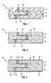
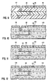
- Figure 1 is a cross-sectional view of a first embodiment of the present invention illustrating a ceramic-filled polymeric composite substrate.
- Figure 2 is a cross-sectional view of a second embodiment of the present invention illustrating a polymer-filled ceramic composite substrate.
- Figure 3 is a cross-sectional view of a variant of the second embodiment of the present invention illustrating a polymer-filled ceramic substrate where the polymer is only located on the surface region and the periphery of the composite substrate and thus encapsulating the entire structure.
- Figure 4 is a flow chart illustrating the method to form the first embodiment of the present invention.
- Figure 5 is a flow chart illustrating the method to form the second embodiment of the present invention.
- Figure 6 is a cross-sectional view similar to Figure 1 but with a surface layer in place for optical transmission of a signal.
- Figure 7 is a cross-sectional view similar to Figure 2 but with a surface layer in place for optical transmission of a signal.
- Figure 8 is a cross-sectional view similar to Figure 3 but with a surface layer in place for optical transmission of a signal.
- Figure 9 is a cross-sectional view similar to Figure 1 but with a layer in place for supporting optical transmission of a signal and a covering surface layer.
- Figure 10 is a cross-sectional view similar to Figure 2 but with a layer in place for supporting optical transmission of a signal and a covering surface layer.
- Figures 11 and 12 are cross-sectional views similar to Figure 3 but with a layer in place for supporting optical transmission of a signal.
- The preferred embodiments of the present invention relate to a composite electronic and/or optical substrate comprising polymeric and ceramic material wherein the substrate has a low dielectric constant and a low CTE. More specifically, the functional requirements for the substrate include low CTE, preferably in the range 8-14ppm/°C at 100°C which is intermediate between the FR-4 PCB (CTE 15-17ppm(in the x,y directions) and 60ppm(in the z direction) and the semiconductor device (CTE 3ppm); dielectric constant < 4, preferably <3.5 to allow for closely spaced high density fine lines/vias; good dimensional stability under thermal stress conditions; improved second level interconnection reliability; and package integrity even with increased die size.
- Similarly, the functional requirements of the polymeric materials useful in the preferred embodiments of the present invention should include low in-plane CTE; low birefringence and isotropic optical and mechanical properties; a low dielectric constant of 3.5 or less; high mechanical strength and high thermal stability at temperatures >300 °C; option for forming laminates/sheets, prepregs, or solution cast films; low melt viscosity suitable for injection molding; layer-to-layer and layer-to-metal adhesion reliability; chemical stability of the polymer-filler composite material under processing conditions; thermo-oxidative stability; and compatibility with photoimaging techniques.
- Representative polymeric materials useful in the composite substrates of the preferred embodiments of the present invention include: thermoplastic polyesters such as polybutylene terephthalate (PBTP), polyethylene naphthalate (PEN), polyarylene ether, and polycarbonate/polybutylene terephthalate blends; liquid crystalline polymer (LCP) polyesters, for example, p-hydroxy benzoic acid (HBA)/p-hydroxy naphthoic acid (HNA); PBTP-LCP, and PEN-LCP blends; polymethyl methacrylate (PMMA); poly (α-methylstyrene); polyvinyl butyral; blends of LCP and polyether imide (PEI), and LCP and polyethersulfone; flexible-planar chain polyimides; low CTE polyimides of rod-like structure; fluorinated polyimides and siloxane polyimides; polyimide/polyester films/laminates such as thermally conductive KAPTON (Dupont trade name), UPILEX (Ube Industries trade name); blends of polyimides with LC polyesters, B-stage glass reinforced polyester sheets; polyphenylene oxide-epoxy (PPO-epoxy) blends (e.g., GETEK laminates available from General Electric); polycyclo-olefins/polynorbornene (e.g., AVATREL resins(trade name, B.F. Goodrich Company); SILK polymers (trade name of Dow Chemical, Inc.); bis-benzocycolobutene polymers, for example, BCB-DVS, (CYCLOTENE resins (trade name, Dow Chemicals); polysilsesquioxanes; and cyanate ester resin, cyanate/epoxy, and BT/epoxy resins, BMI resins (bismaleimides).
- Among the polyimide materials referred to above as one of the polymeric materials suitable for composite substrates according to the preferred embodiments of this invention, a particularly preferred category are low CTE polyimides including BPDA-PDA, BPDA-ODA, PMDA-PDA and partially fluorinated polyimide carrying perfluoroisopropylidene functionality in either anhydride or in the amine segment or in both the anhydride and the amine (e.g., Pyralin RC2566, FPI fluorinated polyimides available from DuPont), partially fluorinated polyimides as PMDA-BDAF, BPDA-BDAF, and BTDA-BDAF derived from 2,2-bis[4-(4-aminophenoxy)phenyl]-hexafluoropropane (BDAF) and 1,2,3,4-tetracarboxylic dianhydride or pyromellitic dianhydride(PMDA), sym-biphenic tetracarboxylic acid dianhydride, and 3,3',4,4'-benzophenone tetracarboxylic acid dianhydride, respectively. Examples of non-fluorinated semi-flexible chain polyimides which can also be used include those derived from PMDA-ODA, e.g., Pyralin RC5878 polyamic acid precursor or KAPTON films available from DuPont, and BPDA-ODA polyamic acid precursor solution or the corresponding preimidized film as Upilex R available from Ube Industries Inc. The typical range of representative properties of the unfilled polyimide films after curing up to 350-400°C include: Tg, greater than 260°C; dielectric constant, 2.9-3.5; Eb% (elongation-at-break), 50-90%; elastic modulus, 2.5-10 GPa; CTE 3-50ppm/°C at 100°C. The partially fluorinated polyimides of the preferred embodiments of this invention have excellent self adhesion and to other polymers and metals, and thus can be used for interlaminate bonding as well as self-bonding composite laminates without requiring an interlaminate bonding layer.
- The low CTE polyimides for the purpose of the the preferred embodiments of present invention are those derived from linear-planar or semiflexible precursors of which preferred candidates are the BPDA-PDA (sym-biphenic- tetracarboxylic acid dianhydride (BPDA)- p-phenylene diamine (PDA)) polyimide solution cast films as well as machine drawn chemically or thermally cured laminates available from Ube Industries under the trade name UPILEX. Because of the rigid-rod or semiflexible-planar molecular structure, this class of polyimides have special properties of low in-plane CTE (about 5 at 100°C and 8 ppm at 300°C), low dielectric constant (2.9-3.1), high modulus (8-11GPa), high tensile strength (400-450MPa), low moisture absorption (less than 1%), and high Tg (>400°C).
- The preferred ceramic materials for the composite substrate have low coefficient of thermal expansion (preferably less than 8 ppm/°C from room temperature to 400°C) and low dielectric constant (preferably less than 6). Some of these ceramic materials may include electronic grade SiO2, silylated silica, quartz, fused silica, Al2O3-SiO2, 3Al2O3.2SiO2 (Mullite), BeO, silicates of Al, Fe or Mg such as 5SiO2-2Al2O3-2MgO (Cordierite), other glasses such as borosilicate glass, and mixtures thereof. The ceramic materials can be in the form of a powder, fiber, sphere, microsphere, hollow sphere, flake, whisker, and the like. For isotropic proprties of polymer-filler composites, particularly CTE in the x, y, and z direction, it is preferred to use a filler in particle form.
- The composite substrates of the preferred embodiments of the present invention can be made by fabricating multiple layers of polymer-ceramic composite green sheets and then laminating them to form the composite substrates. The build of the composite substrate can be accomplished in parallel or sequentially. The composite substrate may have at least one surface layer especially adapted to support high density electronic metal conductors and/or high density optical waveguides for the transmission of electrons and/or photons. As will be described in more detail hereafter, the composite substrate can be made of ceramic-filled polymeric material or polymer-filled ceramic material. The former structure will be described first.
- A composite substrate consisting of layers of ceramic-filled organic polymer composite material, which are metallized using standard techniques, and metal vias for interlayer interconnection can provide a superior packaging structure for high performance semiconductor applications. Methods of forming polymer-filler composites as moldable or sheet castable formulations, and as laminates/B-staged preprepregs are well known in the art. As one empodiment of this invention, a ceramic reinforced polyimide composite is formed by dispersing ceramic filler in a polyamic acid precursor solution which is then converted to molding compound by first solvent removal and then imidization to form polyimide. The molding powder can be compression molded under suitable temperature and pressure conditions to form composite sheets. Alternatively, the polyamic acid-ceramic filler dispersion or slurry can be cast on a carrier sheet by conventional coating processes such as curtain coating, roll coating etc., followed by solvent removal, and optionally partial or complete curing and removal from the carrier to obtain composite prepregs. The ceramic filler content is preferably in the range 10-70wt% based on the ceramic-filled polymer composite material.
- Such a composite multilayer substrate has the advantage of having an intermediate thermal expansion between a semiconductor device (about 3ppm/ °C at 100°C) and a conventional printed circuit board (about 17-18ppm/°C at 100°C). The composite substrate consists of multiple dielectric layers of ceramic-filled polymeric material with via holes filled with an electrically conductive paste or alternatively, the vias can be filled with solid metal to provide interlayer interconnections.
- The composite substrate can be fabricated from parallel processed layers or serial processed layers, or by a combination of the two. For example, the composite substrate could be built in parallel with stacked triplates such as a power core with a signal layer on either side and individual power layers between the cores. At least one suitable top layer could then be added to the composite substrate. Alternatively, a core structure could be formed by sequentially adding layers of dielectric and metal conductors. Then, at least one suitable top layer could be added to the core.
- The metal fillers for conductive pastes for interlayer connections can be, for example, Cu, Ni, Pd or Ag powder with a low melting binary or ternary alloy such as eutectic Bi/Sn, In/Sn, Pb/Sn/Ag, In/Sn on Cu or Ni, Pb/Sn on Cu, Bi/Sn/Pb on Cu, Sn plated Cu, Bi-coated Cu. The conductive paste can constitute 60-90wt% metal filler by weight of the total paste solids which comprises organic binder, conductive particles, additives, and may also include an inorganic component such as glass powder. Surface features are comprised of a high conductivity metal (e.g., Cu) which may have a Ni layer followed by a thin Au plated layer or surface finishing metallurgy for solder connections with the semiconductor device and the PCB.
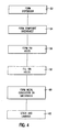
- Referring now to the Figures in more detail, and particularly referring to Figure 4, to form the ceramic-filled polymeric composite substrate, the ceramic fillers are mixed with the polymer matrix in a solvent carrier with appropriate additives such as a plasticizer, surfactant/dispersant, antioxidant and coloring agents to form
dispersion 52. The aforementioned ingredients are mixed in a high shear mixing process using a planetary mixer or a ball mill or a roll mill to provide a homogeneous slurry for casting. For filler wettability and dispersion stability, it is generally desirable to surface modify the filler powder with coupling agents such as organosilanes or organotitanates prior to blending with the polymer binder system. Alternatively, a filler surface modifying agent is mixed with the polymer-solvent vehicle and other additive carrying binder system prior to blending in the ceramic filler. - A typical method for surface modification of filler particles to provide improved interaction with the matrix resin involves blending the ceramic powder with a 0.1-1.0% (wt %) solution of γ-aminopropyl triethoxysilane or A-1100 (Union Carbide) in methanol or ethanol and roll milling at room temperature for a few hours after which the liquid is removed under vacuum, and the treated solids are dried by heating to about 100 °C. Other silane coupling agents for surface modification of the ceramic powder include vinyldimethyl ethoxy silane, vinyl trialkoxy silane, hexamethyl disilazane (HMDS), divinyl tetramethyl disiloxane (DVS) and related materials in the presence of aliphatic amines, e.g., n-propyl amine. An adhesion promoter can be added into the paste components if desired. Preferably, the polymer matrix selected is such that it contains a pendant functionality such as alkoxysilane or vinyl alkoxy silane having an affinity for the ceramic particle surface and thus providing in-situ surface modification. Similarly, organotitanate coupling agents can be used to surface modify the filler prior to blending with the binder system or these can be added to the binder system prior to blending in ceramic filler. Typical titanates commonly used for silica filler modification include isopropyl tri(dioctylpyrophosphato) titanate, isopropyl tri(ethylamino- ethylamino) titanate, and related materials.
- The composite slurry thus formed is cast into sheets (called green sheets) on a carrier, typically PET, polyethylene, or polypropylene backing materials, or prepregs using the commonly practiced sheet casting process (54 in Figure 4). Alternatively, composite polymer prepregs/sheets can be formed by melt-extrusion or injection molding techniques which are well known in the art. In the latter process, solvent-less thermoplastic polymer and inorganic filler blends as molding powder having melt viscosity suitable for injection molding at easily attainable temperature, are compression molded into laminates. In the case of slurry cast sheets, a follow-on drying operation is generally carried out to remove solvent in the cast sheets. Similarly, solvent carrying flexible-chain poly (amic acid) or poly (Amic ester) precursor solutions are filled with ceramic particles, then converted into molding compound by solvent removal and imidization by heating at 100-200 °C and compressive molded to B-stage laminates.
- A blanking operation generates the desired size individual layers of the composite substrate and punches registration holes necessary for alignment. The backing sheet is then removed and vias are formed (56 in Figure 4) in each layer by mechanical punching, laser drilling, mechanical drilling, e-beam machining or chemically etching, then filled with an electrically conductive metal (58 in Figure 4).
- The vias can be filled with a metallic paste as is conventional, for example by screen printing or squeegeeing the paste through a metal mask in contact with the composite laminate. Alternatively, the via metallurgy can be formed by filling with solid metal deposited by known techniques such as plating or subtractive etch, or by mechanically positioning electrically conductive metal spheres. Where the vias are filled by using a conductive paste, the metallized green sheets are dried. Then, the signal and wiring metallization patterns are formed on the surface of the green sheet layer (60 in Figure 4) by screen printing or extrusion screening a conductive paste formulated with low melting metal filler using conventional multilayer ceramic fabrication techniques. Alternatively, the signal and wiring metallization can be formed from solid metal (such as by a decal process) and then transferred to the surface of the layer.
- The metallized layers are subjected to a heating cycle at 100-250°C to remove residual solvent and partially cure (B-stage) or completely cure the resin matrix.
- The individual layers are inspected or electrically tested, then the desired number of layers are aligned and stacked (62 in Figure 4), placing a thin non-stick polymer sheet on the top and bottom layers of the stack, and laminated using a hydraulic uniaxial press at 150-350°C and 200-2000 psi pressure to form a multilayer composite interconnect structure. Subsequently, the laminated structure is subjected to a plating process for surface finishing metal deposition, typically Ni/Au by an electroless process.
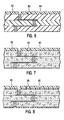
- Prior to surface finishing, at least one surface layer can be added that is especially adapted for supporting high density electronic metal conductors and/or high density optical waveguides for the transmission of electrons and/or photons, respectively, Such a surface layer is shown in Figure 6 as
surface layer 80 having waveguides 82 (e.g., an optical fiber) and/or 84 (e.g., an open channel). The composition of thesurface layer 80 is 30 to 100% by weight polymeric material and 70 to 0% by weight ceramic. - Alternatively, ceramic-filled
polymeric layer 92 can be formed to supportwaveguide 82 and/orchannel 84 as shown in Figure 9. In this embodiment,channel 84 should be lined with alayer 94 of polymeric material. Note thatchannel 84 is left unfilled. Lastly,polymeric surface layer 96 is formed. - Where the surface layers 80, 102 and
liner 94 are to be used for high density optical waveguides and channels, there should be no ceramic filler in the surface layer. The polymeric material should be an optically transparent, low (optical) loss material. Some exemplary materials for the surface layer are fluorinated polymers such as fluorinated and perfluorinated polyimides; acrylic polymers such as fluoroalkyl (methacrylate), perfluoro(methacrylate), and alkylmethacrylate homopolymers/copolymers such as PMMA and PMMA/polystyrene copolymers; polyetherketone; polyesters; and urethane-acrylic polymers. The waveguides can be optical fibers, open channels for optical transmission or optical waveguides. The dielectric material should preferably have a different index of refraction so as to refract the light and keep it within the waveguide. - If there is inadequate interlayer adhesion integrity, a thin layer of an adhesive polymer can be used for interlayer adhesion and bond integrity under various processing and use conditions. By way of illustration and not limitation, various adherants that can be used for bonding polyimide-based composite metallized layers include: acrylics, siloxane polyimides, acetylene terminated polyimides, e.g., IP-610 or IP-615 Thermid-Isoimide series derived from BTDA-APB (3,3',4,4'-tetracarboxylic acid benzophenone dianhydride/ 3,3"- bis-amino phenoxy benzene) polyisoimide oligomers and related 6FDA-APB derived polymers (available from National Starch), bisbenzocyclobutenes, divinylsiloxane-bisbenzocyclobutene polymers, for example, the DVS-bis-BCB polymer (CYCLOTENE resins, trade name of Dow Chemical), 6FDA-ODA and BTDA-ODA polyamic acids (available from DuPont), polyesters, polyalkylacrylates, or low molecular weight aromatic copolyesters or homopolyesters. The polymer adhesion layer interposed between composite layers results in layer-to-layer bonding under the temperature and pressure conditions for the lamination step. In the case of fully cured composite sheets, it is preferred to activate the surface by O2 plasma exposure or by chemical means, e.g., chemical etching prior to applying an adhesion layer by spray, roll coating or any other commonly used surface coating techniques. The adherant coat is then baked to remove solvent or other volatiles and partially dry/cure to form a B-stage cured non-tacky surface. Subsequent processing can then proceed as described above to form via patterns, layer assembly, lamination, and deposition of finishing metallurgy to form an interconnect structure comprising a ceramic-filled polymer composite. Alternatively, the adhesion layer can be a fully cured thermoplastic melt-flowable polymer film which can be bonded to the ceramic-filled polymer composite layer by lamination prior to via punching or laser drilling, using standard techniques similar to the commercially available acrylic adhesive or TEFLON (trade name DuPont) bonded KAPTON (trade name DuPont), bond-ply laminates, PYRALUX (trade name DuPont)thermoplastic laminates, and related materials.
- The finished
composite substrate 10 is illustrated in Figure 1. Multiple layers of ceramic-filledpolymeric material 12 are stacked and laminated so that they are adjacent to one another. Although not shown in Figure 1, an adherent material optionally may be sandwiched between the layers to provide layer-to-layer bonding if necessary. The adherent material should be chosen so as to not degrade but preferably complement the properties (CTE, dielectric constant, Tg, thermal stability, etc.) as mentioned above for the composite substrate. Thecomposite substrate 10 will preferably also comprisevias 14 and wiring lines 16. - The composite substrate is now ready for semiconductor device joining and interconnection to a PCB. Semiconductor joining can use conventional area array interconnections with or without underfill. The connections to the PCB can be made by using conventional surface mount technology such as ball grid arrays (BGA), land grid arrays (LGA) or pluggable interconnections. Benefits of the disclosed structure and process include low cost; dimensional control; low dielectric constant; low impedance; uniformity of feature size for high frequency, thinner dielectric layers; ability to process small feature sizes; and ability to tailor product attributes such as CTE, dielectric constant, toughness, thermal and thermooxidative stability, and desirable electrical and mechanical properties.
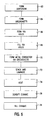
- A second embodiment according to this invention comprises metal conductors and a partially densified ceramic matrix which has been surface sealed or bulk filled with an organic or an organometallic polymer insulator having low dielectric constant, low CTE, and low moisture absorption. Fabrication of this structure can be obtained by using a multilayer-ceramic (MLC) type process involving preparation of a green sheet slurry comprising ceramic filler and a polymer binder system in a solvent vehicle, sheet casting on a carrier and solvent volatilization to form green sheets. After a drying operation to remove the solvent, and blanking operation, the individual layers are patterned for via definition by mechanical punching, laser drilling, mechanical drilling, e-beam machining, or chemically etching. Subsequent steps after via punching involve personalization employing a screen-on metal paste, drying, inspection of individual screened sheets, stacking and alignment, lamination, binder burn-off, densification of metal and partial sintering of the ceramic by subjecting it to an elevated temperature to produce a bisque fired "necked" rigid skeletal network or porous ceramic body. The structure is then treated with an organic or organometallic polymer solution or solvent-free polymerizable reactive monomer/oligomer composition such that it either forms a surface skin-like seal or fills the bulk matrix porosity. Subsequent thermal treatment to remove solvent and curing or polymerization provides a polymer encapsulated structure. Subsequent processing involves deposition of pad metallurgy, electrical test, semiconductor device joining, module electrical test and PCB connections.
- Proportion of the polymer filler relative to the metallized ceramic composite body will depend on the level of porosity in ceramic, the filling of bulk porosity or only the surface region and encapsulation, and the density of metal pattern.
- Preferred polymers for forming the green sheet slurry for the polymer-filled ceramic structure are those which essentially completely depolymerize to monomeric or thermally decompose to monomeric/oligomeric species which volatilize when conventionally heated in a binder burn-off heating cycle to 300-400 °C. Various polymers suitable for this purpose include a poly(alkyl methacrylate), preferably, PMMA [poly(methyl methacrylate)], PMMA-poly-n-butyl methacrylate copolymers, poly(t-butyl methacrylate), PαMS [poly(α-methyl styrene)], polyvinyl butyral, poly(propylene oxide), and PIB [poly( isobutylene)], PMMA-PIB blends, which readily depolymerizes at temperature less than 400°C.
- The electrically conductive metal paste for via fill may comprise a metal powder such as Au, Au-Cu, Au-Sn, Cu-Sn intermetallics, Ag plated Cu, or Au plated Ni, and optionally an inorganic particulate such a glass frit, in a polymer binder system which is readily removable by heating at less than 350-450 °C. The mixture is milled in a roll mill to form an homogeneous paste.
- In order to provide a polymer seal or encapsulation on the surface layers or for filling the porous regions in the bulk of the substrate, the structure is treated with a solvent-less or solvent carrying polymer or pre-polymer solution, preferably a solvent-less reactive oligomer composition, to flow in between the porous region in the ceramic network. For illustrative purposes, BCB resin solution or divinyl siloxane-bis-benzocyclobutene (DVS-BCB) prepolymer solution (CYCLOTENE resins, Dow Chemical Co.) is dispensed over the substrate in multiple applications, heated at 100-150 °C in-between applications to slowly remove solvent or low molecular weight species after each application, and a final cure to 350 °C in a programmed oven or furnace to form a thermally stable, solvent resistant polymer matrix encapsulating the ceramic bulk porosity. The BCB polymers are available as partially polymerized (B-staged) resins in solvent. The cured crosslinked polymers have several advantages, particularly, low dielectric constant (2.65 at 1KHz to 1MHz) and dielectric loss tangent (<0.0008 at 1KHz), resistance to solvents when fully crosslinked, and high thermal stability, and low moisture absorption. Other low viscosity materials can also be used for back filling the ceramic porosity, for example, SILK polymers, polyarylene ether, low molecular weight cross linkable polyorganosilanes, such as poly(methylsilsesquioxane) which can be obtained in solution with high solids, can be dispensed similar to the BCB solution, and baked to temperatures up to 400 °C to form a crosslinked insulating matrix in ceramic skeletal network.
- Examples of other thermosetting polymeric systems that can be used for post-sinter surface seal or bulk impregnation into the necked-ceramic bulk include acetylene terminated polyimides such as Thermid-Isoimide series of materials, for example, IP-610 or 615 oligomers; low CTE polyimides, e.g., BPDA-PDA, BPDA-ODA; bis-maleimide-triazine resins (BT-resin), cyanate ester-epoxy blends, poly(amic ethyl ester) such as PMDA-ODA amic-ethyl ester, BPDA-PDA amic-ethyl ester, and related materials.
- The 'necked' ceramic structure can also be surface sealed by application of a high viscosity polymer and curing to high temperature. Again for illustrative purposes, the substrate is treated with a polyimide composition such as BTDA-ODA, BPDA-ODA, partially fluorinated polyamic acid or poly (amic ester) such as hexafluoro isopropylidene diphthalic anhydride (6FDA) - oxydianiline (ODA) (6FDA-ODA) (RC2566, trade name of DuPont) as about 20% solids in NMP by spray, dip, or other liquid application methods, and baked/cured using a programmed oven or a furnace with N2 purge. Typical temperature profile involves: starting at about 70-80°C followed by a programmed profile using 2-4°C/min ramp rate: ramp to 150°C, 210-240°C, 300°C, with about 20min hold at each temperature, and finally cured at 350-375°C for 45-60 minutes and slow cooling to at least 70-80°C before removing parts. The polyimide solution can also be applied in multiple applications for increasing permeation into the bulk in addition to the surface layers. In that instance, it is preferred that after each application, the polymer be subjected to intermediate bake at about 150°C, and cooled to room temperature before another coating is applied. After the final application, it is subjected to full curing temperature profile up to 350-375°C.
- Referring now to Figure 2, there is disclosed a second embodiment of the present invention.
Composite substrate 20 includes multiple layers of ceramic 22 havingpores 28 which are filled with apolymeric material 30. Theporosity 28 is continuous throughout thecomposite substrate 20 so that thepolymeric material 30 can infiltrate through all of thepores 28. Thecomposite substrate 20 will preferably also comprisevias 24 and wiring lines 26. - A variant of the second embodiment of the invention is shown in Figure 3. There,
composite substrate 20! hasceramic layers 22 withporosity 28. In the case of composite substrate 20', however, thepolymeric material 32 seals the outside of the composite substrate 20' and only partially infiltrates into it, thereby leaving most ofporosity 28 free ofpolymeric material 32.Polymeric material 32 is either removed from, or prevented from depositing in,areas 34 so that electrical connection can be made to a semiconductor device (not shown) or a PCB (not shown). - Referring now to Figure 5, the method of making the second embodiment of the invention will be discussed. Ceramic material is mixed with a polymer binder material in a solvent carrier with appropriate additives such as a plasticizer, surfactant/dispersant, antioxidant and coloring agents to form
dispersion 63, also known as a green sheet slurry. The aforementioned ingredients are mixed in a high shear mixing process using a planetary mixer or a ball mill or a roll mill to provide an homogeneous slurry for casting. For filler wettability with the polymer binder system and dispersion stability, it is generally desirable to surface modify the ceramic material with coupling agents such as organosilanes or organotitanates prior to blending with the polymer. Alternatively, a particle surface modifying agent can be mixed in with the organic binder system and then the ceramic material is blended in to form the composite slurry. The polymer binder is chosen so as to depolymerize as mentioned earlier. - The composite slurry thus formed is cast into sheets (called green sheets) on a carrier, typically PET, polyethylene or polypropylene, using a sheet casting process (64 in Figure 5). After a drying operation to remove solvent in the cast sheets, a blanking operation generates the desired size individual layers of the composite substrate and punches registration holes necessary for alignment.
- The backing sheet material is then removed and vias are formed (66 in Figure 5) in each layer by mechanical punching, laser drilling, or chemically etching, then filled with an electrically conductive metal (68 in Figure 5). The vias can be filled with a metallic paste as is conventional. Alternatively, the via metallurgy can be formed by filling with solid metal deposited by known techniques such as plating or subtractive etch, or by mechanically positioning electrically conductive metal elements, for example, molded or inserted by pressing in metal spheres in position. Where the vias are filled by using an electrically conductive paste, the green sheets are dried to remove volatiles. Then, the signal and wiring metallization patterns are formed on the surface of the green sheet layer (70 in Figure 5) by screen printing or extrusion screening a conductive paste formulated with a metal filler using conventional multilayer ceramic fabrication techniques. Alternatively, the signal and wiring metallization can be formed from solid metal (such as by a decal process) and then transferred to the surface of the green sheet layer.
- The individual layers are inspected and then the desired number of layers are aligned and stacked (72 in Figure 4), placing a thin non-stick polymer sheet on the top and bottom layers of the stack, and laminated using a hydraulic uniaxial press at 150-350°C and 200-2000 psi pressure to form a multilayer composite interconnect structure.
- Thereafter, the ceramic body is heated (74 in Figure 5) to a temperature sufficient to depolymerize the polymer binder and remove the carbonaceous residue in a process which is conventionally known and practiced as binder burnoff. The sintering temperature is then raised to a temperature sufficient for the ceramic to partially densify (76). Partial densification of ceramic or 'bisque' firing generates a porous or skeletal ceramic body as is well known in the ceramic arts. After the now porous ceramic body is cooled to room temperature and removed from the furnace, the polymeric material noted previously is partially or fully infiltrated (78 in Figure 5) into the porous ceramic body. Subsequently, the laminated structure is subjected to a plating process for surface finishing metal deposition, typically Ni/Au by an electroless process.
- Prior to surface finishing, at least one surface layer can be added that is especially adapted for supporting high density electronic metal conductors and/or high density optical waveguides for the transmission of electrons and/or photons, respectively, Such a surface layer is shown in Figures 7 and 8 as
surface layer 86 having waveguides 88 (e.g., an optical fiber) and/or 90 (e.g., an open channel). Figure 7 generally corresponds to Figure 2 but with thesurface layer 86. Similarly, Figure 8 generally corresponds to Figure 3 but with thesurface layer 86. The composition of the surface layers is 30 to 100% by weight polymeric material and 70 to 0% by weight ceramic. - Alternatively, ceramic-filled
polymeric layer 98 can be formed to supportwaveguide 88 and/orchannel 90 as shown in Figures 10 and 11. In this embodiment,channel 90 should be lined with alayer 100 of polymeric material. Note thatchannel 90 is left unfilled. Lastly,polymeric surface layer 102 is formed. - As yet another embodiment as illustrated in Figure 12, sealing
layer 32 shown in Figure 11 can be dispensed with. Then layer 104 can be a ceramic-filled polymeric material or an unfilled ceramic material, similar to the rest of the substrate. Sealing for the substrate would be provided bypolymeric surface layer 102. - Where the surface layers 86,, 102 and
liner 100 are to be used for high density optical waveguides, there should be no ceramic filler in the surface layer. The polymeric material should be an optically transparent, low (optical) loss material. Some exemplary materials for the surface layer are fluorinated polymers such as fluorinated and perfluorinated polyimides; acrylic polymers such as fluoroalkyl (methacrylate), perfluoro(methacrylate), and alkylmethacrylate homopolymers/copolymers such as PMMA and PMMA/polystyrene copolymers; polyetherketone; polyesters; and urethane-acrylic polymers. The waveguides can be optical fibers, open channels for optical transmission or opotical waveguides. The dielectric material should preferably have a different index of refraction so as to refract the light and keep it within the waveguide.
Claims (23)
- A composite substrate comprising a plurality of layers, each of the layers comprising a mixture of a polymeric and a ceramic material, wherein the substrate has a coefficient of thermal expansion of 8 to 14 ppm/ °C at 100°C and a dielectric constant less than 4, said composite substrate being adapted for use as an optical and/or electronic substrate.
- A composite substrate as claimed in claim 1 wherein each of the layers comprises 30 to 90 weight % polymeric material and 10 to 70 weight % ceramic material.
- A composite substrate as claimed in claim 1 wherein each of the layers comprises 40 to 60 weight % polymeric material and 40 to 60 weight % ceramic material.
- A composite substrate as claimed in any preceding claim further comprising a surface layer comprising 100% by weight polymeric material and suitable for supporting at least one optical waveguide.
- A composite substrate as claimed in any preceding claim wherein one of the plurality of adjacent layers supports at least one optical waveguide; and further comprising:a surface layer adjacent to the one of the plurality of layers comprising 100% by weight polymeric material; whereinthe at least one optical waveguide is a channel, the channel further comprising a liner of 100% by weight polymeric material.
- A composite substrate as claimed in any preceding claim wherein the polymeric material is selected from the group consisting of fluorinated polymers, acrylic polymers, polyetherketone, polyesters, and urethane-acrylic polymers.
- A composite substrate as claimed in any preceding claim wherein the ceramic is selected from the group consisting of silica, fused silica, quartz, alumina silicates, magnesia silicates, boria silicates, and mixtures thereof.
- A composite substrate as claimed in any preceding claim wherein the polymeric material is selected from the group consisting of thermoplastic polyesters, LC polyesters, LCP-thermoplastic polymer blends, polyimides, fluorinated polyimides, low thermal expansion polyimides of rod-like structure, thermoplastic polymers, poly(cyclo-olefins), poly(benzocyclobutenes), cyanate ester resins, cynate ester/epoxy blends, bis-maleimide resins, polyvinyl butyral, poly(alkylmethacrylates), poly(alphmethylstyrene) and mixtures thereof.
- A method of making a composite substrate, the method comprising the steps of:forming a dispersion of polymeric and ceramic materials;forming a plurality of composite green sheets with the dispersion;forming via holes in each of the green sheets;filling a metal conductor in the via holes of each of the green sheets;forming a metal conductor on a surface of each of the composite green sheets; andstacking and laminating the plurality of green sheets to form a composite substrate of adjacent composite layers that has a coefficient of thermal expansion of 8 to 14 ppm/ °C at 100°C and a dielectric constant less than 4, the composite substrate being adapted for use as an optical and/or electronic substrate.
- A method as claimed in claim 9 further comprising the step of densifying the metal conductor in the via holes of each of the green sheets or on the surface of each of the green sheets.
- A method as claimed in claim 9 or claim 10 wherein the metal conductor in the via holes of each of the green sheets comprises solid metallic elements or a metal decal.
- A method as claimed in any of claims 9 to 11 wherein the dispersion comprises 30 to 90 weight % polymeric material and 10 to 70 weight % ceramic material.
- A method as claimed in any of claims 9 to 12 wherein the ceramic is selected from the group consisting of silica, fused silica, quartz, alumina silicates, magnesia silicates, boria silicates, and mixtures thereof.
- A method as claimed in any of claims 9 to 13 wherein the polymeric material is selected from the group consisting of thermoplastic polyesters, LC polyesters, polyimides, fluorinated polyimides, low thermal expansion polyimides, poly (arylene ether), thermoplastic polymers, poly(cyclo-olefins), poly(benzocyclobutenes), cyanate ester resins, cynate ester/epoxy blends, bis-maleimide resins, poly(alkylmethacrylates), poly(alphmethylstyrene) and mixtures thereof.
- A method as claimed in any of claims 9 to 14 further comprising the step, prior to the step of stacking and laminating, of forming at least two of the green sheets into a subunit.
- A method as claimed in any of claims 9 to 15 further comprising the step of forming a surface layer suitable for use as an optical waveguide and, after the step of stacking and laminating, bonding the surface layer to the composite substrate.
- A method as claimed in claim 16 wherein the surface layer comprises 100% by weight polymeric material.
- A method as claimed in claim 16 or claim 17 wherein the at least one optical waveguide is a channel, the channel further comprising a liner of 100% by weight polymeric material.
- A method as claimed in any of claims 9 to 18 wherein the polymeric material is selected from the group consisting of fluorinated polymers, acrylic polymers, polyetherketone, polyesters, and urethane-acrylic polymers.
- A method as claimed in any of claims 9 to 19 and further comprising the steps of:heating the composite substrate to thermally remove the polymeric material and any carbonaceous residue;partially densifying the ceramic material to produce a rigid skeletal structure;at least partially filling the rigid skeletal structure with a polymeric material to produce a composite substrate that has a coefficient of thermal expansion of 8 to 14 ppm/ °C and a dielectric constant less than 4, the composite substrate being adapted for use as an optical and/or electronic substrate.
- A method as claimed in claim 20 wherein the step of partially densifying the ceramic material further comprises densifying the metal conductor in the via holes of each of the green sheets or on the surface of each of the green sheets.
- A method as claimed in claim 20 or claim 21 wherein the polymeric material for forming a dispersion of polymeric and ceramic materials is selected from the group consisting of PMMA [poly(methyl methacrylate)], PMMA-poly-n-butyl methacrylate copolymers, poly(t-butyl methacrylate), POMS [poly(α-methyl styrene)], polyvinyl butyral, poly(propylene oxide), PIB [poly( isobutylene)], and PMMA-PIB blends
- A method as claimed in any of claims 20 to 22 wherein the polymeric material for at least partially filling the rigid skeletal ceramic structure is selected from the group consisting of polyimides, fluorinated polyimides, low CTE polyimides, poly (arylene ether), SILK, poly(cyclo-olefins), poly(benzocyclobutenes), cyanate ester resins, cynate ester/epoxy blends, bis-maleimide (BMI) resins and mixtures thereof.
Applications Claiming Priority (2)
| Application Number | Priority Date | Filing Date | Title |
|---|---|---|---|
| US09/606,359 US6528145B1 (en) | 2000-06-29 | 2000-06-29 | Polymer and ceramic composite electronic substrates |
| US606359 | 2000-06-29 |
Publications (2)
| Publication Number | Publication Date |
|---|---|
| EP1168436A2 true EP1168436A2 (en) | 2002-01-02 |
| EP1168436A3 EP1168436A3 (en) | 2008-11-19 |
Family
ID=24427650
Family Applications (1)
| Application Number | Title | Priority Date | Filing Date |
|---|---|---|---|
| EP01305287A Withdrawn EP1168436A3 (en) | 2000-06-29 | 2001-06-18 | Polymer and ceramic composite electronic substrates |
Country Status (7)
| Country | Link |
|---|---|
| US (1) | US6528145B1 (en) |
| EP (1) | EP1168436A3 (en) |
| JP (1) | JP3745653B2 (en) |
| KR (1) | KR100462451B1 (en) |
| CN (1) | CN1170314C (en) |
| MY (1) | MY117336A (en) |
| TW (1) | TW515055B (en) |
Cited By (8)
| Publication number | Priority date | Publication date | Assignee | Title |
|---|---|---|---|---|
| CN1297000C (en) * | 2002-08-14 | 2007-01-24 | 国际商业机器公司 | Interconnection structure containing stress regulating covering and its mfg. method |
| WO2007146383A1 (en) * | 2006-06-15 | 2007-12-21 | E. I. Du Pont De Nemours And Company | Organic encapsulant compositions based on heterocyclic polymers for protection of electronic components |
| WO2011063247A3 (en) * | 2009-11-20 | 2011-09-29 | E. I. Du Pont De Nemours And Company | Interposer films useful in semiconductor packaging applications, and methods relating thereto |
| CN102550136A (en) * | 2009-09-15 | 2012-07-04 | 罗伯特·博世有限公司 | Method for producing a ceramic component, ceramic component and component assembly |
| EP2712027A4 (en) * | 2011-04-28 | 2015-04-22 | Kuang Chi Innovative Tech Ltd | DIELECTRIC SUBSTRATE OF METAMATERIAL, AND PROCESSING METHOD THEREOF |
| US20230317592A1 (en) * | 2022-04-01 | 2023-10-05 | Intel Corporation | Substrate with low-permittivity core and buildup layers |
| WO2025160248A1 (en) * | 2024-01-25 | 2025-07-31 | Yield Engineering Systems, Inc. | Dielectric liners on through glass vias |
| US12543536B2 (en) | 2023-11-27 | 2026-02-03 | Toto Ltd. | Electrostatic chuck |
Families Citing this family (126)
| Publication number | Priority date | Publication date | Assignee | Title |
|---|---|---|---|---|
| WO2000018202A1 (en) * | 1998-09-17 | 2000-03-30 | Ibiden Co., Ltd. | Multilayer build-up wiring board |
| US6875719B2 (en) * | 2000-04-27 | 2005-04-05 | Industrial Technology Research Institute | Catalyst composition for preparing olefin polymers |
| JP4095763B2 (en) * | 2000-09-06 | 2008-06-04 | 株式会社ルネサステクノロジ | Semiconductor device and manufacturing method thereof |
| US6800815B1 (en) | 2001-01-16 | 2004-10-05 | National Semiconductor Corporation | Materials and structure for a high reliability bga connection between LTCC and PB boards |
| US6656313B2 (en) * | 2001-06-11 | 2003-12-02 | International Business Machines Corporation | Structure and method for improved adhesion between two polymer films |
| US6682619B2 (en) * | 2001-07-17 | 2004-01-27 | Sikorsky Aircraft Corporation | Composite pre-preg ply having tailored dielectrical properties and method of fabrication thereof |
| US20030137815A1 (en) * | 2002-01-18 | 2003-07-24 | Matsushita Electric Industrial Co., Ltd. | Printed wiring board and method of manufacturing the same |
| US7714432B2 (en) * | 2002-07-26 | 2010-05-11 | Intel Corporation | Ceramic/organic hybrid substrate |
| KR100483622B1 (en) * | 2002-08-16 | 2005-04-19 | 삼성전기주식회사 | Method for attaching optical waveguide component to printed circuit board |
| JP2005539382A (en) * | 2002-09-16 | 2005-12-22 | ワールド・プロパティーズ・インコーポレイテッド | Liquid crystal polymer composite, method for producing the same, and article formed therefrom |
| JP4426805B2 (en) * | 2002-11-11 | 2010-03-03 | 日本特殊陶業株式会社 | Wiring board and manufacturing method thereof |
| TWI234210B (en) * | 2002-12-03 | 2005-06-11 | Sanyo Electric Co | Semiconductor module and manufacturing method thereof as well as wiring member of thin sheet |
| KR100451635B1 (en) * | 2002-12-10 | 2004-10-08 | 삼성전기주식회사 | Fiber blocks and pipe blocks, and methods for connecting optical signals of multi-layer PCB by using them |
| EP1586592B1 (en) * | 2002-12-25 | 2010-04-21 | Daikin Industries, Ltd. | Fluoropolymer and composition thereof |
| DE10302104A1 (en) * | 2003-01-21 | 2004-08-05 | Friwo Gerätebau Gmbh | Process for the production of circuit carriers with integrated passive components |
| US6764748B1 (en) * | 2003-03-18 | 2004-07-20 | International Business Machines Corporation | Z-interconnections with liquid crystal polymer dielectric films |
| US7265300B2 (en) * | 2003-03-21 | 2007-09-04 | Commscope Solutions Properties, Llc | Next high frequency improvement using hybrid substrates of two materials with different dielectric constant frequency slopes |
| TW573444B (en) * | 2003-04-22 | 2004-01-21 | Ind Tech Res Inst | Substrate having organic and inorganic functional package |
| US7126228B2 (en) * | 2003-04-23 | 2006-10-24 | Micron Technology, Inc. | Apparatus for processing semiconductor devices in a singulated form |
| KR20040106674A (en) * | 2003-06-11 | 2004-12-18 | 삼성전자주식회사 | Structures of optical waveguide laminated printed circuit board and optical connection blocks and method for constructing waveguide layer |
| US7164197B2 (en) * | 2003-06-19 | 2007-01-16 | 3M Innovative Properties Company | Dielectric composite material |
| US7226654B2 (en) * | 2003-07-29 | 2007-06-05 | Kyocera Corporation | Laminated wiring board and its mounting structure |
| US7129318B2 (en) * | 2003-09-02 | 2006-10-31 | I.S.T. (Ma) Corporation | RTM and RI processable polyimide resins |
| JP2005195690A (en) * | 2003-12-26 | 2005-07-21 | Toshiba Corp | Metal-containing resin particles, resin particles, and manufacturing method of electronic circuit |
| US7015075B2 (en) * | 2004-02-09 | 2006-03-21 | Freescale Semiconuctor, Inc. | Die encapsulation using a porous carrier |
| US7342181B2 (en) * | 2004-03-12 | 2008-03-11 | Commscope Inc. Of North Carolina | Maximizing capacitance per unit area while minimizing signal transmission delay in PCB |
| US7429789B2 (en) * | 2004-03-31 | 2008-09-30 | Endicott Interconnect Technologies, Inc. | Fluoropolymer dielectric composition for use in circuitized substrates and circuitized substrate including same |
| US7470990B2 (en) * | 2004-03-31 | 2008-12-30 | Endicott Interconnect Technologies, Inc. | Low moisture absorptive circuitized substrate with reduced thermal expansion, method of making same, electrical assembly utilizing same, and information handling system utilizing same |
| US7190594B2 (en) | 2004-05-14 | 2007-03-13 | Commscope Solutions Properties, Llc | Next high frequency improvement by using frequency dependent effective capacitance |
| US7980900B2 (en) * | 2004-05-14 | 2011-07-19 | Commscope, Inc. Of North Carolina | Next high frequency improvement by using frequency dependent effective capacitance |
| US8221885B2 (en) | 2004-06-02 | 2012-07-17 | Cool Options, Inc. a corporation of the State of New Hampshire | Thermally conductive polymer compositions having low thermal expansion characteristics |
| US20060001145A1 (en) * | 2004-07-03 | 2006-01-05 | Aptos Corporation | Wafer level mounting frame with passive components integration for ball grid array packaging |
| WO2006014582A2 (en) * | 2004-07-08 | 2006-02-09 | Dow Corning Corporation | Short reach optical interconnect |
| DE102004037381A1 (en) * | 2004-08-02 | 2006-03-16 | Patent-Treuhand-Gesellschaft für elektrische Glühlampen mbH | Kittlos capped lamp |
| CN101014890B (en) | 2004-09-08 | 2011-01-19 | 东丽株式会社 | Optical wiring resin composition and photo-electric composite wiring board |
| KR100638620B1 (en) * | 2004-09-23 | 2006-10-26 | 삼성전기주식회사 | Printed Circuit Board Materials for Embedded Passive Devices |
| TW200613447A (en) * | 2004-10-28 | 2006-05-01 | Ind Tech Res Inst | Dielectric constant adjustable resin composition, prepreg and copper clad laminate utilizing the same |
| JP2006128520A (en) * | 2004-10-29 | 2006-05-18 | Tdk Corp | Multilayer substrate manufacturing method |
| JP2006128519A (en) * | 2004-10-29 | 2006-05-18 | Tdk Corp | Multilayer substrate manufacturing method |
| JP2006152173A (en) * | 2004-11-30 | 2006-06-15 | Sumitomo Bakelite Co Ltd | Resin composition, resin layer, carrier material with resin layers and circuit board |
| WO2006074550A1 (en) * | 2005-01-14 | 2006-07-20 | National Research Council Of Canada | Implantable biomimetic prosthetic bone |
| US7352061B2 (en) * | 2005-05-20 | 2008-04-01 | Intel Corporation | Flexible core for enhancement of package interconnect reliability |
| US7095602B1 (en) * | 2005-06-29 | 2006-08-22 | Murata Manufacturing Co., Ltd. | Ceramic structure and nonreciprocal circuit device |
| US7342183B2 (en) * | 2005-07-11 | 2008-03-11 | Endicott Interconnect Technologies, Inc. | Circuitized substrate with sintered paste connections, multilayered substrate assembly, electrical assembly and information handling system utilizing same |
| EP1909322A4 (en) * | 2005-07-27 | 2011-08-03 | Murata Manufacturing Co | STACKED ELECTRONIC COMPONENT, ELECTRONIC DEVICE, AND METHOD FOR MANUFACTURING STACKED ELECTRONIC COMPONENT |
| JP2007096185A (en) * | 2005-09-30 | 2007-04-12 | Sanyo Electric Co Ltd | Circuit board |
| JP5309316B2 (en) * | 2006-02-06 | 2013-10-09 | 国立大学法人東北大学 | Chip element |
| US20070235450A1 (en) * | 2006-03-30 | 2007-10-11 | Advanced Composite Materials Corporation | Composite materials and devices comprising single crystal silicon carbide heated by electromagnetic radiation |
| JP4862893B2 (en) * | 2006-06-02 | 2012-01-25 | 株式会社村田製作所 | Multilayer ceramic electronic component and manufacturing method thereof |
| US7407415B2 (en) * | 2006-06-07 | 2008-08-05 | International Business Machines Corporation | Crosstalk reduction in dual inline memory module (DIMM) connectors |
| KR100752019B1 (en) * | 2006-09-29 | 2007-08-28 | 삼성전기주식회사 | Insulation Materials for Printed Circuit Boards |
| JP5175476B2 (en) * | 2007-02-28 | 2013-04-03 | 三洋電機株式会社 | Circuit device manufacturing method |
| US20080217748A1 (en) * | 2007-03-08 | 2008-09-11 | International Business Machines Corporation | Low cost and low coefficient of thermal expansion packaging structures and processes |
| GB0706638D0 (en) * | 2007-04-04 | 2007-05-16 | Mbda Uk Ltd | A high-dielectric material |
| US20120052222A1 (en) * | 2007-08-10 | 2012-03-01 | Gagne Robert R | Lightweight ballistic protection materials, |
| WO2009045932A1 (en) | 2007-09-28 | 2009-04-09 | Tri-Star Laminates, Inc. | Improved systems and methods for drilling holes in printed circuit boards |
| JP2009098654A (en) * | 2007-09-28 | 2009-05-07 | Dainippon Printing Co Ltd | Optical laminate, polarizing plate, and image display device |
| US20100283570A1 (en) * | 2007-11-14 | 2010-11-11 | Lavoie Adrien R | Nano-encapsulated magnetic particle composite layers for integrated silicon voltage regulators |
| US20100012354A1 (en) * | 2008-07-14 | 2010-01-21 | Logan Brook Hedin | Thermally conductive polymer based printed circuit board |
| WO2010009381A1 (en) * | 2008-07-18 | 2010-01-21 | World Properties, Inc. | Circuit materials, circuits laminates, and method of manufacture thereof |
| KR100983219B1 (en) * | 2008-12-05 | 2010-09-20 | 조근호 | Method of manufacturing printed circuit board by direct printing method and printed circuit board manufactured thereby |
| US8047879B2 (en) * | 2009-01-26 | 2011-11-01 | Commscope, Inc. Of North Carolina | Printed wiring boards and communication connectors having series inductor-capacitor crosstalk compensation circuits that share a common inductor |
| TW201032689A (en) * | 2009-02-20 | 2010-09-01 | Unimicron Technology Corp | Composite circuit substrate structure |
| DE102009024982B4 (en) * | 2009-06-16 | 2013-01-10 | Solarworld Innovations Gmbh | Masking method, use of the method and intermediate and method for producing a contact structure for a semiconductor device |
| KR20110019536A (en) * | 2009-08-20 | 2011-02-28 | 삼성전기주식회사 | Ceramic substrate and its manufacturing method |
| KR101123900B1 (en) * | 2009-08-28 | 2012-03-23 | 한국세라믹기술원 | Composite material and its fabrication method |
| CN102117670B (en) * | 2009-10-29 | 2016-05-04 | 住友金属矿山株式会社 | Resistor material, resistance film form by sputtering target, resistance film, thin film resistor and their manufacture method |
| JP4929423B2 (en) | 2010-07-22 | 2012-05-09 | 日本碍子株式会社 | Molded body and method for producing molded body |
| US20120286416A1 (en) * | 2011-05-11 | 2012-11-15 | Tessera Research Llc | Semiconductor chip package assembly and method for making same |
| EP2737275A4 (en) | 2011-07-28 | 2014-09-17 | Mac Llc | Polymeric ammunition casing geometry |
| US9182204B2 (en) | 2011-07-28 | 2015-11-10 | Mac, Llc | Subsonic ammunition casing |
| DE102011080299B4 (en) * | 2011-08-02 | 2016-02-11 | Infineon Technologies Ag | Method of manufacturing a circuit carrier, and method of manufacturing a semiconductor device |
| WO2013042749A1 (en) * | 2011-09-22 | 2013-03-28 | 日立化成株式会社 | Laminated body, laminated board, multi-layer laminated board, printed wiring board, and production method for laminated board |
| JPWO2013042751A1 (en) * | 2011-09-22 | 2015-03-26 | 日立化成株式会社 | LAMINATE, LAMINATE, MULTILAYER LAMINATE, PRINTED WIRING BOARD AND METHOD FOR PRODUCING LAMINATE |
| US9101061B2 (en) * | 2011-09-22 | 2015-08-04 | Hitachi Chemical Company, Ltd. | Laminate body, laminate plate, multilayer laminate plate, printed wiring board, and method for manufacture of laminate plate |
| US10543662B2 (en) | 2012-02-08 | 2020-01-28 | Corning Incorporated | Device modified substrate article and methods for making |
| FR2988223B1 (en) * | 2012-03-19 | 2016-09-02 | Solarwell | LIGHT EMITTING DEVICE CONTAINING APLATISED ANISOTROPIC SEMICONDUCTOR COLLOIDAL NANOCRISTALS AND PROCESS FOR PRODUCING SUCH DEVICES |
| RU2639315C2 (en) * | 2012-07-12 | 2017-12-21 | ЛЭЙБИНЕЛ, ЭлЭлСи | Packaging of load tires and method of its manufacture |
| TWI617437B (en) | 2012-12-13 | 2018-03-11 | 康寧公司 | Facilitated processing for controlling bonding between sheet and carrier |
| US10086584B2 (en) | 2012-12-13 | 2018-10-02 | Corning Incorporated | Glass articles and methods for controlled bonding of glass sheets with carriers |
| US9340443B2 (en) | 2012-12-13 | 2016-05-17 | Corning Incorporated | Bulk annealing of glass sheets |
| TW201429708A (en) * | 2012-12-13 | 2014-08-01 | Corning Inc | Glass and methods of making glass articles |
| US10014177B2 (en) | 2012-12-13 | 2018-07-03 | Corning Incorporated | Methods for processing electronic devices |
| JP6377074B2 (en) * | 2012-12-20 | 2018-08-22 | ダウ グローバル テクノロジーズ エルエルシー | Polymer composite components for wireless communication towers |
| KR20140091346A (en) * | 2013-01-11 | 2014-07-21 | 삼성디스플레이 주식회사 | Display apparatus and method for manufacturing the same |
| US10510576B2 (en) | 2013-10-14 | 2019-12-17 | Corning Incorporated | Carrier-bonding methods and articles for semiconductor and interposer processing |
| AT515069B1 (en) * | 2013-11-07 | 2019-10-15 | At & S Austria Tech & Systemtechnik Ag | Printed circuit board structure |
| ES2728242T3 (en) | 2014-01-13 | 2019-10-23 | Mac Llc | Polymeric Ammo Pod |
| WO2015112958A1 (en) | 2014-01-27 | 2015-07-30 | Corning Incorporated | Articles and methods for controlled bonding of thin sheets with carriers |
| US9453714B2 (en) | 2014-04-04 | 2016-09-27 | Mac, Llc | Method for producing subsonic ammunition casing |
| CN106457758B (en) | 2014-04-09 | 2018-11-16 | 康宁股份有限公司 | The modified substrate article and preparation method thereof of device |
| US9379298B2 (en) * | 2014-10-03 | 2016-06-28 | Henkel IP & Holding GmbH | Laminate sub-mounts for LED surface mount package |
| CN107635769B (en) | 2015-05-19 | 2020-09-15 | 康宁股份有限公司 | Article and method for bonding sheet to carrier |
| JP7106276B2 (en) | 2015-06-26 | 2022-07-26 | コーニング インコーポレイテッド | Articles and methods with sheets and carriers |
| US10008382B2 (en) | 2015-07-30 | 2018-06-26 | Taiwan Semiconductor Manufacturing Company, Ltd. | Semiconductor device having a porous low-k structure |
| KR20170025021A (en) * | 2015-08-27 | 2017-03-08 | 삼성전기주식회사 | Resin-coated copper foil for use in manufacturing of printed circuit board and method for manufacturing printed circuit board using same |
| WO2017069752A1 (en) * | 2015-10-21 | 2017-04-27 | Hewlett-Packard Development Company, L.P. | Three-dimensional (3d) printing |
| US11367959B2 (en) | 2015-10-28 | 2022-06-21 | Rogers Corporation | Broadband multiple layer dielectric resonator antenna and method of making the same |
| US10476164B2 (en) | 2015-10-28 | 2019-11-12 | Rogers Corporation | Broadband multiple layer dielectric resonator antenna and method of making the same |
| US10374315B2 (en) | 2015-10-28 | 2019-08-06 | Rogers Corporation | Broadband multiple layer dielectric resonator antenna and method of making the same |
| US20170287838A1 (en) | 2016-04-02 | 2017-10-05 | Intel Corporation | Electrical interconnect bridge |
| WO2018022447A1 (en) * | 2016-07-27 | 2018-02-01 | Corning Incorporated | Ceramic and polymer composite, methods of making, and uses thereof |
| TW202216444A (en) | 2016-08-30 | 2022-05-01 | 美商康寧公司 | Siloxane plasma polymers for sheet bonding |
| TWI810161B (en) | 2016-08-31 | 2023-08-01 | 美商康寧公司 | Articles of controllably bonded sheets and methods for making same |
| KR20190097141A (en) * | 2016-12-16 | 2019-08-20 | 사빅 글로벌 테크놀러지스 비.브이. | Structured ceramic composite made by natural materials and cold sintering |
| CN106876357B (en) * | 2017-01-24 | 2024-11-15 | 深圳市槟城电子股份有限公司 | Electrode for chip packaging and chip packaging structure using the electrode |
| CN106604536B (en) * | 2017-01-26 | 2019-05-21 | 上海安缔诺科技有限公司 | Polytetrafluoroethylene (PTFE) composite microwave medium material and preparation method thereof |
| US11075130B2 (en) | 2017-03-30 | 2021-07-27 | Intel Corporation | Package substrate having polymer-derived ceramic core |
| US11876295B2 (en) | 2017-05-02 | 2024-01-16 | Rogers Corporation | Electromagnetic reflector for use in a dielectric resonator antenna system |
| US11283189B2 (en) * | 2017-05-02 | 2022-03-22 | Rogers Corporation | Connected dielectric resonator antenna array and method of making the same |
| KR102312067B1 (en) | 2017-06-07 | 2021-10-13 | 로저스코포레이션 | Dielectric Resonator Antenna System |
| JP7260523B2 (en) | 2017-08-18 | 2023-04-18 | コーニング インコーポレイテッド | Temporary binding using polycationic polymers |
| US11331692B2 (en) | 2017-12-15 | 2022-05-17 | Corning Incorporated | Methods for treating a substrate and method for making articles comprising bonded sheets |
| US11616302B2 (en) | 2018-01-15 | 2023-03-28 | Rogers Corporation | Dielectric resonator antenna having first and second dielectric portions |
| US10892544B2 (en) | 2018-01-15 | 2021-01-12 | Rogers Corporation | Dielectric resonator antenna having first and second dielectric portions |
| US10910722B2 (en) | 2018-01-15 | 2021-02-02 | Rogers Corporation | Dielectric resonator antenna having first and second dielectric portions |
| RU2715085C2 (en) * | 2018-07-02 | 2020-02-25 | Виталий Евгеньевич Поляков | Active medium for fibre lasers and method for production thereof |
| US11426818B2 (en) | 2018-08-10 | 2022-08-30 | The Research Foundation for the State University | Additive manufacturing processes and additively manufactured products |
| US11031697B2 (en) | 2018-11-29 | 2021-06-08 | Rogers Corporation | Electromagnetic device |
| CN113169455A (en) | 2018-12-04 | 2021-07-23 | 罗杰斯公司 | Dielectric electromagnetic structure and method of manufacturing the same |
| KR20200080992A (en) | 2018-12-27 | 2020-07-07 | 삼성전자주식회사 | Composite, article, battery case, and battery |
| US11482790B2 (en) | 2020-04-08 | 2022-10-25 | Rogers Corporation | Dielectric lens and electromagnetic device with same |
| CN111534820B (en) * | 2020-06-15 | 2021-03-23 | 北京师范大学 | Self-supporting insulating medium and preparation method and application thereof |
| CN115508919A (en) * | 2021-06-22 | 2022-12-23 | 瑞仪光电(南京)有限公司 | Optical film, backlight module, display device and manufacturing method of optical film |
| CN114911003B (en) * | 2022-05-31 | 2023-09-22 | 上海大学 | Optical waveguide preparation method based on cladding ultraviolet lithography |
| US20240222211A1 (en) * | 2022-12-29 | 2024-07-04 | Intel Corporation | Ic die packages with low cte dielectric materials |
Family Cites Families (38)
| Publication number | Priority date | Publication date | Assignee | Title |
|---|---|---|---|---|
| US4680220A (en) * | 1985-02-26 | 1987-07-14 | W. L. Gore & Associates, Inc. | Dielectric materials |
| EP0196865B1 (en) * | 1985-03-27 | 1990-09-12 | Ibiden Co, Ltd. | Electronic circuit substrates |
| JPH0634435B2 (en) * | 1985-11-27 | 1994-05-02 | イビデン株式会社 | Multilayer substrate for electronic circuits |
| US4810563A (en) * | 1986-03-14 | 1989-03-07 | The Bergquist Company | Thermally conductive, electrically insulative laminate |
| US5384181B1 (en) | 1987-02-17 | 2000-06-13 | World Properties Inc | Low volume fraction ceramic filled fluoropolymeric composite material |
| US5061548A (en) | 1987-02-17 | 1991-10-29 | Rogers Corporation | Ceramic filled fluoropolymeric composite material |
| US4849284A (en) * | 1987-02-17 | 1989-07-18 | Rogers Corporation | Electrical substrate material |
| EP0309982A3 (en) * | 1987-09-30 | 1990-09-12 | E.I. Du Pont De Nemours And Company | Polymer-ceramic composite plies |
| US5139852A (en) * | 1988-03-11 | 1992-08-18 | International Business Machines Corporation | Low dielectric composite substrate |
| JPH02148789A (en) * | 1988-03-11 | 1990-06-07 | Internatl Business Mach Corp <Ibm> | Electronic circuit board |
| JPH0811781B2 (en) * | 1988-03-26 | 1996-02-07 | 松下電工株式会社 | Shaped high dielectric polyphenylene oxide resin composition |
| JPH088416B2 (en) * | 1988-10-25 | 1996-01-29 | 日本電気株式会社 | Method for manufacturing ceramic multilayer circuit board |
| JPH03177376A (en) * | 1989-12-04 | 1991-08-01 | Japan Gore Tex Inc | Ceramic board |
| US5213878A (en) * | 1990-03-23 | 1993-05-25 | Minnesota Mining And Manufacturing Company | Ceramic composite for electronic applications |
| JPH0491497A (en) * | 1990-08-02 | 1992-03-24 | Sumitomo Chem Co Ltd | Manufacture of wiring board consisting of ceramic resin composite body |
| JPH04103349A (en) * | 1990-08-23 | 1992-04-06 | Hitachi Chem Co Ltd | Manufacture of metal plated thermoplastic resin layered board |
| US5541249A (en) | 1990-12-18 | 1996-07-30 | Hoechst Celanese Corp. | Injection moldable ceramic and metallic compositions and method of preparing the same |
| US5287619A (en) | 1992-03-09 | 1994-02-22 | Rogers Corporation | Method of manufacture multichip module substrate |
| JP3287871B2 (en) * | 1992-04-01 | 2002-06-04 | ソニー株式会社 | Printed circuit board manufacturing method |
| JPH05291706A (en) * | 1992-04-13 | 1993-11-05 | Mitsubishi Gas Chem Co Inc | Manufacturing method of printed wiring board |
| JPH06219819A (en) * | 1993-01-20 | 1994-08-09 | Asahi Glass Co Ltd | Ceramic green sheet and ceramic substrate |
| JPH06281831A (en) * | 1993-03-25 | 1994-10-07 | Nippon Telegr & Teleph Corp <Ntt> | Electric wiring/optical wiring combined flexible printed circuit board and substrate therefor |
| US5358775A (en) | 1993-07-29 | 1994-10-25 | Rogers Corporation | Fluoropolymeric electrical substrate material exhibiting low thermal coefficient of dielectric constant |
| JP3442895B2 (en) * | 1994-07-04 | 2003-09-02 | 新光電気工業株式会社 | Sintered body for substrate production, substrate and method for producing the same |
| DE69417027T2 (en) * | 1994-08-02 | 2000-01-05 | Mitsubishi Gas Chemical Co., Inc. | Process for the production of a raw board for printed circuit boards |
| US5571609A (en) | 1994-10-13 | 1996-11-05 | Rogers Corporation | Polybutadiene and polyisoprene based thermosetting compositions and method of manufacture thereof |
| JPH08125339A (en) * | 1994-10-21 | 1996-05-17 | Kyocera Corp | Method for manufacturing multilayer wiring board |
| JP3199584B2 (en) * | 1994-10-31 | 2001-08-20 | 京セラ株式会社 | Multilayer wiring board |
| US5552210A (en) * | 1994-11-07 | 1996-09-03 | Rogers Corporation | Ceramic filled composite polymeric electrical substrate material exhibiting high dielectric constant and low thermal coefficient of dielectric constant |
| JPH08186376A (en) * | 1994-12-28 | 1996-07-16 | Hitachi Ltd | High-density thin-film multilayer wiring board, its mounting structure, and its manufacturing method |
| JPH08231274A (en) * | 1995-02-24 | 1996-09-10 | Kyocera Corp | Resin-ceramic composite material and electronic circuit board using the same |
| US5670262A (en) * | 1995-05-09 | 1997-09-23 | The Dow Chemical Company | Printing wiring board(s) having polyimidebenzoxazole dielectric layer(s) and the manufacture thereof |
| US5919546A (en) * | 1995-06-22 | 1999-07-06 | Shinko Electric Industries Co. Ltd. | Porous ceramic impregnated wiring body |
| JPH10100320A (en) * | 1996-09-30 | 1998-04-21 | Mitsubishi Gas Chem Co Inc | Composite ceramic plate and manufacturing method thereof |
| US5965273A (en) * | 1997-01-31 | 1999-10-12 | Hoechst Celanese Corporation | Polymeric compositions having a temperature-stable dielectric constant |
| US5922453A (en) * | 1997-02-06 | 1999-07-13 | Rogers Corporation | Ceramic-filled fluoropolymer composite containing polymeric powder for high frequency circuit substrates |
| US6845184B1 (en) * | 1998-10-09 | 2005-01-18 | Fujitsu Limited | Multi-layer opto-electronic substrates with electrical and optical interconnections and methods for making |
| US6233817B1 (en) * | 1999-01-17 | 2001-05-22 | Delphi Technologies, Inc. | Method of forming thick-film hybrid circuit on a metal circuit board |
-
2000
- 2000-06-29 US US09/606,359 patent/US6528145B1/en not_active Expired - Lifetime
-
2001
- 2001-06-18 KR KR10-2001-0034264A patent/KR100462451B1/en not_active Expired - Fee Related
- 2001-06-18 EP EP01305287A patent/EP1168436A3/en not_active Withdrawn
- 2001-06-21 MY MYPI20012928A patent/MY117336A/en unknown
- 2001-06-26 JP JP2001193284A patent/JP3745653B2/en not_active Expired - Fee Related
- 2001-06-26 TW TW090115463A patent/TW515055B/en not_active IP Right Cessation
- 2001-06-28 CN CNB011218142A patent/CN1170314C/en not_active Expired - Fee Related
Cited By (10)
| Publication number | Priority date | Publication date | Assignee | Title |
|---|---|---|---|---|
| CN1297000C (en) * | 2002-08-14 | 2007-01-24 | 国际商业机器公司 | Interconnection structure containing stress regulating covering and its mfg. method |
| WO2007146383A1 (en) * | 2006-06-15 | 2007-12-21 | E. I. Du Pont De Nemours And Company | Organic encapsulant compositions based on heterocyclic polymers for protection of electronic components |
| CN102550136A (en) * | 2009-09-15 | 2012-07-04 | 罗伯特·博世有限公司 | Method for producing a ceramic component, ceramic component and component assembly |
| WO2011063247A3 (en) * | 2009-11-20 | 2011-09-29 | E. I. Du Pont De Nemours And Company | Interposer films useful in semiconductor packaging applications, and methods relating thereto |
| CN102714192A (en) * | 2009-11-20 | 2012-10-03 | E.I.内穆尔杜邦公司 | Interconnect conductive thin films for use in semiconductor packaging applications and related methods |
| US8653512B2 (en) | 2009-11-20 | 2014-02-18 | E. I. Du Pont De Nemours And Company | Thin film transistor compositions, and methods relating thereto |
| EP2712027A4 (en) * | 2011-04-28 | 2015-04-22 | Kuang Chi Innovative Tech Ltd | DIELECTRIC SUBSTRATE OF METAMATERIAL, AND PROCESSING METHOD THEREOF |
| US20230317592A1 (en) * | 2022-04-01 | 2023-10-05 | Intel Corporation | Substrate with low-permittivity core and buildup layers |
| US12543536B2 (en) | 2023-11-27 | 2026-02-03 | Toto Ltd. | Electrostatic chuck |
| WO2025160248A1 (en) * | 2024-01-25 | 2025-07-31 | Yield Engineering Systems, Inc. | Dielectric liners on through glass vias |
Also Published As
| Publication number | Publication date |
|---|---|
| US6528145B1 (en) | 2003-03-04 |
| KR100462451B1 (en) | 2004-12-17 |
| CN1330403A (en) | 2002-01-09 |
| EP1168436A3 (en) | 2008-11-19 |
| CN1170314C (en) | 2004-10-06 |
| JP2002134926A (en) | 2002-05-10 |
| KR20020002216A (en) | 2002-01-09 |
| TW515055B (en) | 2002-12-21 |
| MY117336A (en) | 2004-06-30 |
| JP3745653B2 (en) | 2006-02-15 |
Similar Documents
| Publication | Publication Date | Title |
|---|---|---|
| US6528145B1 (en) | Polymer and ceramic composite electronic substrates | |
| EP0902048B1 (en) | High dielectric constant flexible polyimide film and process of preparation | |
| US6254971B1 (en) | Resin-having metal foil for multilayered wiring board, process for producing the same, multilayered wiring board, and electronic device | |
| US7198996B2 (en) | Component built-in module and method for producing the same | |
| EP1360067B1 (en) | Lightweight circuit board with conductive constraining cores | |
| JP5344022B2 (en) | Epoxy resin composition, prepreg, laminate, resin sheet, printed wiring board, and semiconductor device | |
| US20040256731A1 (en) | Dielectric composite material | |
| KR20130089235A (en) | Prepreg, wiring board, and semiconductor device | |
| KR102056303B1 (en) | Resin composition for semiconductor package, prepreg and metal clad laminate using the same | |
| KR102669464B1 (en) | Materials for printed circuit boards | |
| Sundaram et al. | Next-generation microvia and global wiring technologies for SOP | |
| EP1030543B1 (en) | Non-woven fabric material and prepreg, and circuit board using the same | |
| JPH02116196A (en) | Ceramic multilayer circuit board and its manufacture | |
| JP4422555B2 (en) | Conductive paste composition for multilayer wiring board | |
| KR102712135B1 (en) | Thermosetting resin composition for preparing prepreg, prepreg, and metal clad laminate | |
| KR20060130585A (en) | Thermoplastic composition, substrate material and substrate film | |
| JP4075569B2 (en) | Printed wiring board manufacturing material, printed wiring board and manufacturing method thereof | |
| JP3694673B2 (en) | Insulating film and multilayer wiring board using the same | |
| JP2003069238A (en) | Insulating film and multilayer wiring board using the same | |
| JP2004179011A (en) | Insulating film and multilayer wiring board using the same | |
| JPH05167211A (en) | Laminated board for printed circuit and manufacture thereof | |
| JP2004082554A (en) | Insulating film and multilayer wiring board using the same | |
| JP2004090238A (en) | Insulating film and multilayer wiring board using the same | |
| JP2003174264A (en) | Insulating film and multilayer wiring board using the same | |
| JP2003062942A (en) | Insulating film and multilayer wiring board using the same |
Legal Events
| Date | Code | Title | Description |
|---|---|---|---|
| PUAI | Public reference made under article 153(3) epc to a published international application that has entered the european phase |
Free format text: ORIGINAL CODE: 0009012 |
|
| AK | Designated contracting states |
Kind code of ref document: A2 Designated state(s): AT BE CH CY DE DK ES FI FR GB GR IE IT LI LU MC NL PT SE TR |
|
| AX | Request for extension of the european patent |
Free format text: AL;LT;LV;MK;RO;SI |
|
| PUAL | Search report despatched |
Free format text: ORIGINAL CODE: 0009013 |
|
| AK | Designated contracting states |
Kind code of ref document: A3 Designated state(s): AT BE CH CY DE DK ES FI FR GB GR IE IT LI LU MC NL PT SE TR |
|
| AX | Request for extension of the european patent |
Extension state: AL LT LV MK RO SI |
|
| 17P | Request for examination filed |
Effective date: 20090122 |
|
| 17Q | First examination report despatched |
Effective date: 20090305 |
|
| AKX | Designation fees paid |
Designated state(s): AT BE CH CY DE DK ES FI FR GB GR IE IT LI LU MC NL PT SE TR |
|
| STAA | Information on the status of an ep patent application or granted ep patent |
Free format text: STATUS: THE APPLICATION IS DEEMED TO BE WITHDRAWN |
|
| 18D | Application deemed to be withdrawn |
Effective date: 20090716 |