EP1132977A2 - Dispositif semiconducteur émetteur de lumière et procédé de fabrication - Google Patents
Dispositif semiconducteur émetteur de lumière et procédé de fabrication Download PDFInfo
- Publication number
- EP1132977A2 EP1132977A2 EP01105380A EP01105380A EP1132977A2 EP 1132977 A2 EP1132977 A2 EP 1132977A2 EP 01105380 A EP01105380 A EP 01105380A EP 01105380 A EP01105380 A EP 01105380A EP 1132977 A2 EP1132977 A2 EP 1132977A2
- Authority
- EP
- European Patent Office
- Prior art keywords
- light emitting
- layer
- semiconductor
- type
- substrate
- Prior art date
- Legal status (The legal status is an assumption and is not a legal conclusion. Google has not performed a legal analysis and makes no representation as to the accuracy of the status listed.)
- Withdrawn
Links
- 239000004065 semiconductor Substances 0.000 title claims abstract description 391
- 238000004519 manufacturing process Methods 0.000 title claims abstract description 40
- 238000000034 method Methods 0.000 title claims abstract description 38
- 238000002347 injection Methods 0.000 claims abstract description 28
- 239000007924 injection Substances 0.000 claims abstract description 28
- 239000000758 substrate Substances 0.000 claims description 144
- 238000005253 cladding Methods 0.000 claims description 126
- 239000000463 material Substances 0.000 claims description 64
- 229910001218 Gallium arsenide Inorganic materials 0.000 claims description 62
- 229910052594 sapphire Inorganic materials 0.000 claims description 20
- 239000010980 sapphire Substances 0.000 claims description 20
- 238000005468 ion implantation Methods 0.000 claims description 17
- 238000005530 etching Methods 0.000 claims description 7
- IJGRMHOSHXDMSA-UHFFFAOYSA-N Atomic nitrogen Chemical compound N#N IJGRMHOSHXDMSA-UHFFFAOYSA-N 0.000 claims description 6
- 150000002500 ions Chemical class 0.000 claims description 6
- 229910052757 nitrogen Inorganic materials 0.000 claims description 3
- OKTJSMMVPCPJKN-UHFFFAOYSA-N Carbon Chemical compound [C] OKTJSMMVPCPJKN-UHFFFAOYSA-N 0.000 claims description 2
- PXGOKWXKJXAPGV-UHFFFAOYSA-N Fluorine Chemical compound FF PXGOKWXKJXAPGV-UHFFFAOYSA-N 0.000 claims description 2
- NINIDFKCEFEMDL-UHFFFAOYSA-N Sulfur Chemical compound [S] NINIDFKCEFEMDL-UHFFFAOYSA-N 0.000 claims description 2
- QVGXLLKOCUKJST-UHFFFAOYSA-N atomic oxygen Chemical compound [O] QVGXLLKOCUKJST-UHFFFAOYSA-N 0.000 claims description 2
- 229910052799 carbon Inorganic materials 0.000 claims description 2
- 229910052731 fluorine Inorganic materials 0.000 claims description 2
- 239000011737 fluorine Substances 0.000 claims description 2
- 229910052760 oxygen Inorganic materials 0.000 claims description 2
- 239000001301 oxygen Substances 0.000 claims description 2
- 229910052717 sulfur Inorganic materials 0.000 claims description 2
- 239000011593 sulfur Substances 0.000 claims description 2
- 230000006866 deterioration Effects 0.000 abstract description 9
- 239000010410 layer Substances 0.000 description 349
- 239000010408 film Substances 0.000 description 25
- JMASRVWKEDWRBT-UHFFFAOYSA-N Gallium nitride Chemical compound [Ga]#N JMASRVWKEDWRBT-UHFFFAOYSA-N 0.000 description 17
- 239000000203 mixture Substances 0.000 description 17
- 230000007423 decrease Effects 0.000 description 14
- SBIBMFFZSBJNJF-UHFFFAOYSA-N selenium;zinc Chemical compound [Se]=[Zn] SBIBMFFZSBJNJF-UHFFFAOYSA-N 0.000 description 12
- -1 ZnSe compound Chemical class 0.000 description 11
- 239000013078 crystal Substances 0.000 description 11
- QAOWNCQODCNURD-UHFFFAOYSA-N Sulfuric acid Chemical compound OS(O)(=O)=O QAOWNCQODCNURD-UHFFFAOYSA-N 0.000 description 10
- 229910002704 AlGaN Inorganic materials 0.000 description 9
- 238000006243 chemical reaction Methods 0.000 description 7
- 238000002488 metal-organic chemical vapour deposition Methods 0.000 description 7
- 230000005855 radiation Effects 0.000 description 7
- 239000012298 atmosphere Substances 0.000 description 5
- 238000010586 diagram Methods 0.000 description 5
- 238000002156 mixing Methods 0.000 description 5
- 230000015572 biosynthetic process Effects 0.000 description 4
- 230000003247 decreasing effect Effects 0.000 description 4
- 230000003287 optical effect Effects 0.000 description 4
- 239000003960 organic solvent Substances 0.000 description 4
- 239000011347 resin Substances 0.000 description 4
- 229920005989 resin Polymers 0.000 description 4
- 239000010409 thin film Substances 0.000 description 4
- 229910007709 ZnTe Inorganic materials 0.000 description 3
- 238000010521 absorption reaction Methods 0.000 description 3
- 239000000853 adhesive Substances 0.000 description 3
- 230000001070 adhesive effect Effects 0.000 description 3
- 230000007547 defect Effects 0.000 description 3
- 238000002474 experimental method Methods 0.000 description 3
- 239000007789 gas Substances 0.000 description 3
- 229910052737 gold Inorganic materials 0.000 description 3
- 239000002184 metal Substances 0.000 description 3
- 229910052751 metal Inorganic materials 0.000 description 3
- KRHYYFGTRYWZRS-UHFFFAOYSA-N Fluorane Chemical compound F KRHYYFGTRYWZRS-UHFFFAOYSA-N 0.000 description 2
- VYPSYNLAJGMNEJ-UHFFFAOYSA-N Silicium dioxide Chemical compound O=[Si]=O VYPSYNLAJGMNEJ-UHFFFAOYSA-N 0.000 description 2
- 239000012790 adhesive layer Substances 0.000 description 2
- 229910045601 alloy Inorganic materials 0.000 description 2
- 239000000956 alloy Substances 0.000 description 2
- 229910052782 aluminium Inorganic materials 0.000 description 2
- 238000000137 annealing Methods 0.000 description 2
- 239000000969 carrier Substances 0.000 description 2
- 230000008859 change Effects 0.000 description 2
- 229910052802 copper Inorganic materials 0.000 description 2
- 238000009396 hybridization Methods 0.000 description 2
- 238000005286 illumination Methods 0.000 description 2
- 238000002513 implantation Methods 0.000 description 2
- 229910052738 indium Inorganic materials 0.000 description 2
- 239000011261 inert gas Substances 0.000 description 2
- 230000010354 integration Effects 0.000 description 2
- 238000005498 polishing Methods 0.000 description 2
- 230000008569 process Effects 0.000 description 2
- 238000005086 pumping Methods 0.000 description 2
- 229910052709 silver Inorganic materials 0.000 description 2
- 239000002356 single layer Substances 0.000 description 2
- 230000003746 surface roughness Effects 0.000 description 2
- 230000001131 transforming effect Effects 0.000 description 2
- 238000013459 approach Methods 0.000 description 1
- 125000004429 atom Chemical group 0.000 description 1
- 238000004140 cleaning Methods 0.000 description 1
- 229910052681 coesite Inorganic materials 0.000 description 1
- 239000003086 colorant Substances 0.000 description 1
- 238000013329 compounding Methods 0.000 description 1
- 150000001875 compounds Chemical class 0.000 description 1
- 238000006482 condensation reaction Methods 0.000 description 1
- 238000010276 construction Methods 0.000 description 1
- 229910052906 cristobalite Inorganic materials 0.000 description 1
- 230000000694 effects Effects 0.000 description 1
- 238000011156 evaluation Methods 0.000 description 1
- 230000005284 excitation Effects 0.000 description 1
- 229910052733 gallium Inorganic materials 0.000 description 1
- 238000010438 heat treatment Methods 0.000 description 1
- 238000002955 isolation Methods 0.000 description 1
- 230000004048 modification Effects 0.000 description 1
- 238000012986 modification Methods 0.000 description 1
- 229910052759 nickel Inorganic materials 0.000 description 1
- 230000009467 reduction Effects 0.000 description 1
- 239000000377 silicon dioxide Substances 0.000 description 1
- 229910052682 stishovite Inorganic materials 0.000 description 1
- 238000002834 transmittance Methods 0.000 description 1
- 229910052905 tridymite Inorganic materials 0.000 description 1
- 238000009966 trimming Methods 0.000 description 1
Images


Classifications
-
- H—ELECTRICITY
- H01—ELECTRIC ELEMENTS
- H01L—SEMICONDUCTOR DEVICES NOT COVERED BY CLASS H10
- H01L33/00—Semiconductor devices having potential barriers specially adapted for light emission; Processes or apparatus specially adapted for the manufacture or treatment thereof or of parts thereof; Details thereof
- H01L33/02—Semiconductor devices having potential barriers specially adapted for light emission; Processes or apparatus specially adapted for the manufacture or treatment thereof or of parts thereof; Details thereof characterised by the semiconductor bodies
- H01L33/26—Materials of the light emitting region
- H01L33/30—Materials of the light emitting region containing only elements of Group III and Group V of the Periodic Table
-
- H—ELECTRICITY
- H01—ELECTRIC ELEMENTS
- H01L—SEMICONDUCTOR DEVICES NOT COVERED BY CLASS H10
- H01L33/00—Semiconductor devices having potential barriers specially adapted for light emission; Processes or apparatus specially adapted for the manufacture or treatment thereof or of parts thereof; Details thereof
- H01L33/005—Processes
- H01L33/0093—Wafer bonding; Removal of the growth substrate
-
- H—ELECTRICITY
- H01—ELECTRIC ELEMENTS
- H01L—SEMICONDUCTOR DEVICES NOT COVERED BY CLASS H10
- H01L33/00—Semiconductor devices having potential barriers specially adapted for light emission; Processes or apparatus specially adapted for the manufacture or treatment thereof or of parts thereof; Details thereof
- H01L33/02—Semiconductor devices having potential barriers specially adapted for light emission; Processes or apparatus specially adapted for the manufacture or treatment thereof or of parts thereof; Details thereof characterised by the semiconductor bodies
- H01L33/26—Materials of the light emitting region
- H01L33/30—Materials of the light emitting region containing only elements of Group III and Group V of the Periodic Table
- H01L33/32—Materials of the light emitting region containing only elements of Group III and Group V of the Periodic Table containing nitrogen
-
- H—ELECTRICITY
- H01—ELECTRIC ELEMENTS
- H01L—SEMICONDUCTOR DEVICES NOT COVERED BY CLASS H10
- H01L25/00—Assemblies consisting of a plurality of individual semiconductor or other solid state devices ; Multistep manufacturing processes thereof
- H01L25/03—Assemblies consisting of a plurality of individual semiconductor or other solid state devices ; Multistep manufacturing processes thereof all the devices being of a type provided for in the same subgroup of groups H01L27/00 - H01L33/00, or in a single subclass of H10K, H10N, e.g. assemblies of rectifier diodes
- H01L25/04—Assemblies consisting of a plurality of individual semiconductor or other solid state devices ; Multistep manufacturing processes thereof all the devices being of a type provided for in the same subgroup of groups H01L27/00 - H01L33/00, or in a single subclass of H10K, H10N, e.g. assemblies of rectifier diodes the devices not having separate containers
- H01L25/075—Assemblies consisting of a plurality of individual semiconductor or other solid state devices ; Multistep manufacturing processes thereof all the devices being of a type provided for in the same subgroup of groups H01L27/00 - H01L33/00, or in a single subclass of H10K, H10N, e.g. assemblies of rectifier diodes the devices not having separate containers the devices being of a type provided for in group H01L33/00
- H01L25/0756—Stacked arrangements of devices
-
- H—ELECTRICITY
- H01—ELECTRIC ELEMENTS
- H01L—SEMICONDUCTOR DEVICES NOT COVERED BY CLASS H10
- H01L2924/00—Indexing scheme for arrangements or methods for connecting or disconnecting semiconductor or solid-state bodies as covered by H01L24/00
- H01L2924/0001—Technical content checked by a classifier
- H01L2924/0002—Not covered by any one of groups H01L24/00, H01L24/00 and H01L2224/00
-
- H—ELECTRICITY
- H01—ELECTRIC ELEMENTS
- H01L—SEMICONDUCTOR DEVICES NOT COVERED BY CLASS H10
- H01L33/00—Semiconductor devices having potential barriers specially adapted for light emission; Processes or apparatus specially adapted for the manufacture or treatment thereof or of parts thereof; Details thereof
- H01L33/48—Semiconductor devices having potential barriers specially adapted for light emission; Processes or apparatus specially adapted for the manufacture or treatment thereof or of parts thereof; Details thereof characterised by the semiconductor body packages
- H01L33/50—Wavelength conversion elements
- H01L33/501—Wavelength conversion elements characterised by the materials, e.g. binder
- H01L33/502—Wavelength conversion materials
Definitions
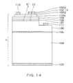
- a GaAs substrate (a second substrate) 101 is cleaned with an organic solvent and/or a sulfuric acid containing etchant, and then, the GaAs substrate 101 is introduced into an MOCVD system. Then, the GaAs substrate 101 is heated to 730°C, and an appropriate 5-Group material serving as a P material is supplied to sequentially grow a light emitting layer 102 of an InAlP/InGaAlP multilayer film and an InAlP cladding layer 103. Further a GaAs cap layer 112 is grown on the surface thereof. The GaAs cap layer 112 is a protection layer which is finally removed. The thickness of these layers are shown in the following table 1. InAlP/InGaAlP Light Emitting Layer 102 30 nm / 50 nm InAlP Cladding Layer 103 300 nm or less GaAs Cap Layer 113 100 nm
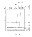
- the bottom side of the sapphire substrate 104 of the semiconductor light emitting element 1 in FIG. 3 is aligned with the top side of the InAlP cladding layer 103 of the semiconductor laminate 2 in FIG. 2.
- the semiconductor light emitting element 1 is aligned with the semiconductor laminate 2
- they are annealed at 500°C in an atmosphere of nitrogen for 30 minutes to be bonded to each other by a dehydrating condensation reaction.
- the surfaces to be bonded are preferably as flat as possible.
- the GaAs substrate 101 inclined in a direction of [011] from the plane (100) is effectively used.
- a GaAs substrate 301 is cleaned with an organic solvent and/or a sulfuric acid containing etchant, and then, the substrate is introduced into an MOCVD system. Then, the substrate is heated to 730°C, and an appropriate 5-Group material serving as a P material is supplied to sequentially crystal-grow a second light emitting layer 302 of an InAlP/InGaAlP multilayer film, a first InAlP cladding layer 303, a first light emitting layer 304 of an InAlP/InGaAlP multilayer film, and a second InAlP cladding layer 305 to further grow a GaAs cap layer 307 on the surface thereof to obtain a stacked structure shown in FIG. 6.
- the GaAs cap layer 307 is a protection layer which is ultimately removed.
- the semiconductor laminate 2 has a structure wherein an InGaAlP light emitting layer 102c is located between a p-type InGaAlP cladding layer 102b and an n-type InGaAlP cladding layer 102a.
- the light emitting layer 102c is designed to emit the yellow light E2 by controlling the composition ratio of 3-Group elements, In, Ga and Al, of InGaAlP.
- the thickness of the light emitting layer 102 is preferably in the range of from 1 nm to 10 ⁇ m.
- FIG. 12 is an xy chromaticity diagram defined by International Commission on Illumination (CIE).
- CIE International Commission on Illumination
- the emission wavelength of an InGaAlN active layer, such as the active layer 107a of the semiconductor light emitting element 1 of FIG. 11, can be in the range of from 380 nm to 500 nm as shown on the left side of FIG. 12.
- the emission wavelength of an InGaAlP light emitting layer, such as the light emitting layer 102c of the semiconductor laminate 2 can be in the range of from 540 nm to 750 nm as shown on the right side of FIG. 12.
- the low-pass filter 130 When the low-pass filter 130 is provided as in the device in this preferred embodiment, it is possible to efficiently extract yellow light emitted from the light emitting layer 107, so that it is possible to further enhance luminance.
Landscapes
- Engineering & Computer Science (AREA)
- Manufacturing & Machinery (AREA)
- Computer Hardware Design (AREA)
- Microelectronics & Electronic Packaging (AREA)
- Power Engineering (AREA)
- Led Devices (AREA)
Priority Applications (1)
| Application Number | Priority Date | Filing Date | Title |
|---|---|---|---|
| EP08000975A EP1921686A3 (fr) | 2000-03-10 | 2001-03-09 | Dispositif électroluminescent semi-conducteur et son procédé de fabrication |
Applications Claiming Priority (4)
| Application Number | Priority Date | Filing Date | Title |
|---|---|---|---|
| JP2000066736 | 2000-03-10 | ||
| JP2000066736A JP4044261B2 (ja) | 2000-03-10 | 2000-03-10 | 半導体発光素子及びその製造方法 |
| JP2000396957 | 2000-12-27 | ||
| JP2000396957A JP4008656B2 (ja) | 2000-12-27 | 2000-12-27 | 半導体発光装置 |
Related Child Applications (1)
| Application Number | Title | Priority Date | Filing Date |
|---|---|---|---|
| EP08000975A Division EP1921686A3 (fr) | 2000-03-10 | 2001-03-09 | Dispositif électroluminescent semi-conducteur et son procédé de fabrication |
Publications (2)
| Publication Number | Publication Date |
|---|---|
| EP1132977A2 true EP1132977A2 (fr) | 2001-09-12 |
| EP1132977A3 EP1132977A3 (fr) | 2003-05-07 |
Family
ID=26587190
Family Applications (2)
| Application Number | Title | Priority Date | Filing Date |
|---|---|---|---|
| EP08000975A Withdrawn EP1921686A3 (fr) | 2000-03-10 | 2001-03-09 | Dispositif électroluminescent semi-conducteur et son procédé de fabrication |
| EP01105380A Withdrawn EP1132977A3 (fr) | 2000-03-10 | 2001-03-09 | Dispositif semiconducteur émetteur de lumière et procédé de fabrication |
Family Applications Before (1)
| Application Number | Title | Priority Date | Filing Date |
|---|---|---|---|
| EP08000975A Withdrawn EP1921686A3 (fr) | 2000-03-10 | 2001-03-09 | Dispositif électroluminescent semi-conducteur et son procédé de fabrication |
Country Status (4)
| Country | Link |
|---|---|
| US (3) | US6576933B2 (fr) |
| EP (2) | EP1921686A3 (fr) |
| CN (2) | CN100541836C (fr) |
| TW (1) | TW497277B (fr) |
Cited By (11)
| Publication number | Priority date | Publication date | Assignee | Title |
|---|---|---|---|---|
| WO2003071610A1 (fr) * | 2002-02-25 | 2003-08-28 | Mitsubishi Cable Industries, Ltd. | Dispositif de source lumineuse et luminaire en faisant usage |
| EP1394867A2 (fr) * | 2002-09-02 | 2004-03-03 | SAMSUNG ELECTRO-MECHANICS Co. Ltd. | Diode électroluminescente et méthode de fabrication |
| DE10354936A1 (de) * | 2003-09-30 | 2005-04-28 | Osram Opto Semiconductors Gmbh | Strahlungemittierendes Halbleiterbauelement |
| EP1601026A2 (fr) | 2004-05-28 | 2005-11-30 | Osram Opto Semiconductors GmbH | Dispositif semi-conducteur optoélectronique et son procédé de fabrication |
| DE102005008056A1 (de) * | 2004-12-30 | 2006-07-13 | Osram Opto Semiconductors Gmbh | Strahlungsemittierender Halbleiterchip und Verfahren zur Herstellung eines solchen Halbleiterchips |
| US7423296B2 (en) | 2003-02-26 | 2008-09-09 | Avago Technologies Ecbu Ip Pte Ltd | Apparatus for producing a spectrally-shifted light output from a light emitting device utilizing thin-film luminescent layers |
| WO2009039815A1 (fr) * | 2007-09-28 | 2009-04-02 | Osram Opto Semiconductors Gmbh | Corps semi-conducteur émettant un rayonnement |
| DE102009020127A1 (de) * | 2009-03-25 | 2010-09-30 | Osram Opto Semiconductors Gmbh | Leuchtdiode |
| WO2015181072A1 (fr) * | 2014-05-27 | 2015-12-03 | Osram Opto Semiconductors Gmbh | Composant semi-conducteur et dispositif d'éclairage |
| FR3075468A1 (fr) * | 2017-12-19 | 2019-06-21 | Commissariat A L'energie Atomique Et Aux Energies Alternatives | Procede de fabrication d'un dispositif optoelectronique par report d'une structure de conversion sur une structure d'emission |
| WO2019141586A1 (fr) * | 2018-01-18 | 2019-07-25 | Osram Opto Semiconductors Gmbh | Élément de conversion épitaxique, puce semi-conductrice émettrice de rayonnement et leur procédé de fabrication |
Families Citing this family (81)
| Publication number | Priority date | Publication date | Assignee | Title |
|---|---|---|---|---|
| US8829546B2 (en) * | 1999-11-19 | 2014-09-09 | Cree, Inc. | Rare earth doped layer or substrate for light conversion |
| JP4101468B2 (ja) * | 2001-04-09 | 2008-06-18 | 豊田合成株式会社 | 発光装置の製造方法 |
| US6958497B2 (en) | 2001-05-30 | 2005-10-25 | Cree, Inc. | Group III nitride based light emitting diode structures with a quantum well and superlattice, group III nitride based quantum well structures and group III nitride based superlattice structures |
| JP3791765B2 (ja) * | 2001-06-08 | 2006-06-28 | 豊田合成株式会社 | Iii族窒化物系化合物半導体発光素子 |
| US7067849B2 (en) * | 2001-07-17 | 2006-06-27 | Lg Electronics Inc. | Diode having high brightness and method thereof |
| US6949395B2 (en) * | 2001-10-22 | 2005-09-27 | Oriol, Inc. | Method of making diode having reflective layer |
| US7148520B2 (en) | 2001-10-26 | 2006-12-12 | Lg Electronics Inc. | Diode having vertical structure and method of manufacturing the same |
| US6841802B2 (en) | 2002-06-26 | 2005-01-11 | Oriol, Inc. | Thin film light emitting diode |
| US7112825B2 (en) * | 2002-07-11 | 2006-09-26 | Rohm Co., Ltd. | Semiconductor light emitting device |
| TW544958B (en) * | 2002-07-15 | 2003-08-01 | Epistar Corp | Light emitting diode with an adhesive layer and its manufacturing method |
| JP2004153241A (ja) * | 2002-10-11 | 2004-05-27 | Sharp Corp | 半導体発光素子及びその製造方法 |
| JP3813123B2 (ja) * | 2002-12-25 | 2006-08-23 | 株式会社沖データ | 半導体装置及びledヘッド |
| TWI226138B (en) * | 2003-01-03 | 2005-01-01 | Super Nova Optoelectronics Cor | GaN-based LED vertical device structure and the manufacturing method thereof |
| JP3717480B2 (ja) * | 2003-01-27 | 2005-11-16 | ローム株式会社 | 半導体発光装置 |
| CN100380688C (zh) * | 2003-03-05 | 2008-04-09 | 联铨科技股份有限公司 | 混色发光二极管 |
| US7268370B2 (en) | 2003-06-05 | 2007-09-11 | Matsushita Electric Industrial Co., Ltd. | Phosphor, semiconductor light emitting device, and fabrication method thereof |
| KR100631832B1 (ko) * | 2003-06-24 | 2006-10-09 | 삼성전기주식회사 | 백색 발광소자 및 그 제조방법 |
| TWI307945B (en) * | 2003-07-15 | 2009-03-21 | Macroblock Inc | A light-emitting semiconductor device packaged with light-emitting diodes and current-driving integrated circuits |
| KR101087854B1 (ko) * | 2003-09-19 | 2011-11-30 | 파나소닉 주식회사 | 반도체 발광장치 |
| JP4085953B2 (ja) * | 2003-10-22 | 2008-05-14 | 住友電気工業株式会社 | 半導体光素子 |
| US7417264B2 (en) * | 2003-12-22 | 2008-08-26 | Samsung Electronics Co., Ltd. | Top-emitting nitride-based light emitting device and method of manufacturing the same |
| KR100506741B1 (ko) * | 2003-12-24 | 2005-08-08 | 삼성전기주식회사 | 플립칩용 질화물 반도체 발광소자 및 그 제조방법 |
| US7569863B2 (en) * | 2004-02-19 | 2009-08-04 | Panasonic Corporation | Semiconductor light emitting device |
| JP2005268770A (ja) | 2004-02-19 | 2005-09-29 | Matsushita Electric Ind Co Ltd | 白色発光素子及び白色光源 |
| US7227192B2 (en) * | 2004-03-31 | 2007-06-05 | Tekcove Co., Ltd | Light-emitting device and manufacturing process of the light-emitting device |
| US20050274971A1 (en) * | 2004-06-10 | 2005-12-15 | Pai-Hsiang Wang | Light emitting diode and method of making the same |
| CN100483757C (zh) * | 2004-06-18 | 2009-04-29 | 皇家飞利浦电子股份有限公司 | Led和具有led的系统及led的制备方法 |
| US7719015B2 (en) * | 2004-12-09 | 2010-05-18 | 3M Innovative Properties Company | Type II broadband or polychromatic LED's |
| US7745814B2 (en) * | 2004-12-09 | 2010-06-29 | 3M Innovative Properties Company | Polychromatic LED's and related semiconductor devices |
| US7402831B2 (en) * | 2004-12-09 | 2008-07-22 | 3M Innovative Properties Company | Adapting short-wavelength LED's for polychromatic, broadband, or “white” emission |
| TWI245440B (en) * | 2004-12-30 | 2005-12-11 | Ind Tech Res Inst | Light emitting diode |
| JP4699764B2 (ja) * | 2005-01-05 | 2011-06-15 | スタンレー電気株式会社 | 半導体発光素子 |
| US7045375B1 (en) | 2005-01-14 | 2006-05-16 | Au Optronics Corporation | White light emitting device and method of making same |
| CN100438095C (zh) * | 2005-01-14 | 2008-11-26 | 财团法人工业技术研究院 | 一种具准全方位反射器的发光二极管 |
| JP4837295B2 (ja) * | 2005-03-02 | 2011-12-14 | 株式会社沖データ | 半導体装置、led装置、ledヘッド、及び画像形成装置 |
| KR100691177B1 (ko) * | 2005-05-31 | 2007-03-09 | 삼성전기주식회사 | 백색 발광소자 |
| CN100389496C (zh) * | 2005-11-04 | 2008-05-21 | 友达光电股份有限公司 | 白光发光元件及其制造方法 |
| JP4137936B2 (ja) * | 2005-11-16 | 2008-08-20 | 昭和電工株式会社 | 窒化ガリウム系化合物半導体発光素子 |
| US7659544B2 (en) * | 2005-12-23 | 2010-02-09 | Hong Kong Applied Science And Technology Research Institute Co., Ltd. | Light emitting device with at least two alternately driven light emitting diodes |
| KR100771811B1 (ko) * | 2005-12-27 | 2007-10-30 | 삼성전기주식회사 | 백색 발광 장치 |
| FR2898434B1 (fr) * | 2006-03-13 | 2008-05-23 | Centre Nat Rech Scient | Diode electroluminescente blanche monolithique |
| US20070284565A1 (en) * | 2006-06-12 | 2007-12-13 | 3M Innovative Properties Company | Led device with re-emitting semiconductor construction and optical element |
| KR100770440B1 (ko) | 2006-08-29 | 2007-10-26 | 삼성전기주식회사 | 질화물 반도체 발광소자 |
| DE102006046037B4 (de) * | 2006-09-28 | 2024-05-29 | OSRAM Opto Semiconductors Gesellschaft mit beschränkter Haftung | LED-Halbleiterkörper und Verwendung eines LED-Halbleiterkörpers |
| US9018619B2 (en) * | 2006-10-09 | 2015-04-28 | Cree, Inc. | Quantum wells for light conversion |
| DE102007010244A1 (de) * | 2007-02-02 | 2008-08-07 | Osram Opto Semiconductors Gmbh | Anordnung und Verfahren zur Erzeugung von Mischlicht |
| US8346002B2 (en) * | 2007-07-20 | 2013-01-01 | Microsoft Corporation | High dynamic range image hallucination |
| JP2009141093A (ja) * | 2007-12-06 | 2009-06-25 | Toshiba Corp | 発光素子及び発光素子の製造方法 |
| DE102008025160A1 (de) * | 2008-05-26 | 2009-12-03 | Osram Opto Semiconductors Gmbh | Projektor für kleinste Projektionsflächen und Verwendung einer Mehrfarben-LED in einem Projektor |
| US7919780B2 (en) * | 2008-08-05 | 2011-04-05 | Dicon Fiberoptics, Inc. | System for high efficiency solid-state light emissions and method of manufacture |
| JP2012526391A (ja) | 2009-05-05 | 2012-10-25 | スリーエム イノベイティブ プロパティズ カンパニー | インジウム空乏機構を利用してインジウム含有基板上で成長した半導体素子 |
| US9293622B2 (en) | 2009-05-05 | 2016-03-22 | 3M Innovative Properties Company | Re-emitting semiconductor carrier devices for use with LEDs and methods of manufacture |
| CN102473817A (zh) | 2009-06-30 | 2012-05-23 | 3M创新有限公司 | 无镉再发光半导体构造 |
| JP5728007B2 (ja) | 2009-06-30 | 2015-06-03 | スリーエム イノベイティブ プロパティズ カンパニー | 電流集中に基づく色調整を伴うエレクトロルミネセント素子 |
| CN102474932B (zh) | 2009-06-30 | 2015-12-16 | 3M创新有限公司 | 具有可调节色温的白光电致发光器件 |
| TWI384657B (zh) * | 2009-07-15 | 2013-02-01 | Ind Tech Res Inst | 氮化物半導體發光二極體元件 |
| US8604461B2 (en) * | 2009-12-16 | 2013-12-10 | Cree, Inc. | Semiconductor device structures with modulated doping and related methods |
| US8536615B1 (en) | 2009-12-16 | 2013-09-17 | Cree, Inc. | Semiconductor device structures with modulated and delta doping and related methods |
| US8575592B2 (en) * | 2010-02-03 | 2013-11-05 | Cree, Inc. | Group III nitride based light emitting diode structures with multiple quantum well structures having varying well thicknesses |
| EP2541626B1 (fr) * | 2010-02-26 | 2019-07-03 | Nichia Corporation | Élément électroluminescent à semi-conducteur au nitrure et son procédé de fabrication |
| CN102194947B (zh) * | 2010-03-17 | 2015-11-25 | Lg伊诺特有限公司 | 发光器件和发光器件封装 |
| CN102918662B (zh) | 2010-05-31 | 2015-11-25 | 日亚化学工业株式会社 | 发光装置及其制造方法 |
| JP5095785B2 (ja) * | 2010-08-09 | 2012-12-12 | 株式会社東芝 | 半導体発光素子及びその製造方法 |
| US20120049151A1 (en) * | 2010-08-30 | 2012-03-01 | Invenlux Corporation | Light-emitting devices with two-dimensional composition-fluctuation active-region and method for fabricating the same |
| JP2012204397A (ja) * | 2011-03-23 | 2012-10-22 | Toshiba Corp | 半導体発光装置およびその製造方法 |
| US8912554B2 (en) | 2011-06-08 | 2014-12-16 | Micron Technology, Inc. | Long wavelength light emitting device with photoluminescence emission and high quantum efficiency |
| TWI547208B (zh) * | 2012-03-19 | 2016-08-21 | 友達光電股份有限公司 | 有機電致發光裝置 |
| US9685585B2 (en) | 2012-06-25 | 2017-06-20 | Cree, Inc. | Quantum dot narrow-band downconverters for high efficiency LEDs |
| CN102820416B (zh) * | 2012-09-10 | 2015-04-01 | 天津三安光电有限公司 | 暖白光发光二极管及其制作方法 |
| CN104347764A (zh) * | 2013-07-31 | 2015-02-11 | 郝炼 | 一种新型GaN基单芯片白光发光二极管器件及其制作方法 |
| WO2015171456A1 (fr) | 2014-05-08 | 2015-11-12 | 3M Innovative Properties Company | Ruban adhésif autocollant avec noyau élastomère microstructuré |
| CN103996755B (zh) * | 2014-05-21 | 2016-08-17 | 天津三安光电有限公司 | 一种氮化物发光二极管组件的制备方法 |
| KR102376468B1 (ko) * | 2014-12-23 | 2022-03-21 | 엘지이노텍 주식회사 | 적색 발광소자 및 조명장치 |
| CN104518056B (zh) * | 2014-12-31 | 2017-05-10 | 山东浪潮华光光电子股份有限公司 | 一种反极性AlGaInP红光LED芯片的制备方法 |
| DE102016101442A1 (de) * | 2016-01-27 | 2017-07-27 | Osram Opto Semiconductors Gmbh | Konversionselement und strahlungsemittierendes Halbleiterbauelement mit einem solchen Konversionselement |
| DE102016104280A1 (de) | 2016-03-09 | 2017-09-14 | Osram Opto Semiconductors Gmbh | Bauelement und Verfahren zur Herstellung eines Bauelements |
| JP6805674B2 (ja) * | 2016-09-21 | 2020-12-23 | 豊田合成株式会社 | 発光素子及びその製造方法 |
| US10868213B2 (en) * | 2018-06-26 | 2020-12-15 | Lumileds Llc | LED utilizing internal color conversion with light extraction enhancements |
| CN109037405B (zh) * | 2018-07-16 | 2020-11-13 | 厦门三安光电有限公司 | 微发光装置及其显示器 |
| DE102018124473A1 (de) | 2018-10-04 | 2020-04-09 | Osram Opto Semiconductors Gmbh | Optoelektronisches bauteil, verfahren zur ansteuerung eines optoelektronischen bauteils und beleuchtungsvorrichtung |
| US11637219B2 (en) | 2019-04-12 | 2023-04-25 | Google Llc | Monolithic integration of different light emitting structures on a same substrate |
Citations (6)
| Publication number | Priority date | Publication date | Assignee | Title |
|---|---|---|---|---|
| EP0486052A1 (fr) * | 1990-11-16 | 1992-05-20 | Daido Tokushuko Kabushiki Kaisha | Diode émettrice de lumière pour émettre simultanément des lumières de longueurs d'onde différentes |
| US5952680A (en) * | 1994-10-11 | 1999-09-14 | International Business Machines Corporation | Monolithic array of light emitting diodes for the generation of light at multiple wavelengths and its use for multicolor display applications |
| EP0971421A2 (fr) * | 1998-07-09 | 2000-01-12 | Sumitomo Electric Industries, Ltd. | Diode émettrice de lumière blanche et diode émettrice de lumière en couleur neutre |
| EP0977278A2 (fr) * | 1998-07-28 | 2000-02-02 | Sumitomo Electric Industries, Ltd. | DEL avec substrat fluorescent |
| WO2000044053A1 (fr) * | 1999-01-25 | 2000-07-27 | Osram Opto Semiconductors Gmbh & Co. Ohg | Composant a semi-conducteur utilise pour la production d'un rayonnement electromagnetique a couleurs melangees |
| WO2000076005A1 (fr) * | 1999-06-04 | 2000-12-14 | Trustees Of Boston University | Diodes electroluminescentes a longueurs d'ondes multiples de semi-conducteur a recyclage de photons |
Family Cites Families (40)
| Publication number | Priority date | Publication date | Assignee | Title |
|---|---|---|---|---|
| US3821590A (en) * | 1971-03-29 | 1974-06-28 | Northern Electric Co | Encapsulated solid state light emitting device |
| JPS48102585A (fr) * | 1972-04-04 | 1973-12-22 | ||
| JPS5127988B2 (fr) * | 1972-09-05 | 1976-08-16 | ||
| US4284884A (en) * | 1980-04-09 | 1981-08-18 | Northern Telecom Limited | Electro-optic devices |
| US4740987A (en) * | 1986-06-30 | 1988-04-26 | American Telephone And Telegraph Company, At&T Bell Laboratories | Distributed-feedback laser having enhanced mode selectivity |
| DE4011145A1 (de) * | 1990-04-06 | 1991-10-10 | Telefunken Electronic Gmbh | Lumineszenz-halbleiterelement |
| DE69333250T2 (de) * | 1992-07-23 | 2004-09-16 | Toyoda Gosei Co., Ltd. | Lichtemittierende Vorrichtung aus einer Verbindung der Galliumnitridgruppe |
| JP3217490B2 (ja) * | 1992-09-29 | 2001-10-09 | 株式会社東芝 | 半導体発光装置 |
| US5488233A (en) * | 1993-03-11 | 1996-01-30 | Kabushiki Kaisha Toshiba | Semiconductor light-emitting device with compound semiconductor layer |
| JPH0794781A (ja) * | 1993-09-24 | 1995-04-07 | Toshiba Corp | 面発光型半導体発光ダイオード |
| JPH07254732A (ja) * | 1994-03-15 | 1995-10-03 | Toshiba Corp | 半導体発光装置 |
| JPH0832110A (ja) * | 1994-07-19 | 1996-02-02 | Oki Electric Ind Co Ltd | 端面発光型led、端面発光型発光素子の製造方法、端面発光型発光素子の発光特性測定方法 |
| US5625201A (en) * | 1994-12-12 | 1997-04-29 | Motorola | Multiwavelength LED devices and methods of fabrication |
| US5661074A (en) * | 1995-02-03 | 1997-08-26 | Advanced Technology Materials, Inc. | High brightness electroluminescent device emitting in the green to ultraviolet spectrum and method of making the same |
| JPH08288549A (ja) | 1995-04-11 | 1996-11-01 | Omron Corp | 多波長発光半導体素子 |
| US5739554A (en) * | 1995-05-08 | 1998-04-14 | Cree Research, Inc. | Double heterojunction light emitting diode with gallium nitride active layer |
| JPH0971421A (ja) | 1995-09-07 | 1997-03-18 | Toda Kogyo Corp | 黄色系顔料用含水酸化第二鉄粒子粉末の製造法 |
| US5710441A (en) * | 1995-10-30 | 1998-01-20 | Motorola, Inc. | Microcavity LED with photon recycling |
| JP3240926B2 (ja) | 1996-06-25 | 2001-12-25 | 日立電線株式会社 | 発光素子 |
| JP2927279B2 (ja) | 1996-07-29 | 1999-07-28 | 日亜化学工業株式会社 | 発光ダイオード |
| US5955749A (en) * | 1996-12-02 | 1999-09-21 | Massachusetts Institute Of Technology | Light emitting device utilizing a periodic dielectric structure |
| US6274890B1 (en) * | 1997-01-15 | 2001-08-14 | Kabushiki Kaisha Toshiba | Semiconductor light emitting device and its manufacturing method |
| JPH10261818A (ja) * | 1997-03-19 | 1998-09-29 | Fujitsu Ltd | 発光半導体装置 |
| US6229160B1 (en) * | 1997-06-03 | 2001-05-08 | Lumileds Lighting, U.S., Llc | Light extraction from a semiconductor light-emitting device via chip shaping |
| JP3617587B2 (ja) * | 1997-07-17 | 2005-02-09 | 日亜化学工業株式会社 | 発光ダイオード及びその形成方法 |
| JPH11154774A (ja) * | 1997-08-05 | 1999-06-08 | Canon Inc | 面発光半導体デバイスの製造方法、この方法によって製造された面発光半導体デバイス及びこのデバイスを用いた表示装置 |
| US6340824B1 (en) * | 1997-09-01 | 2002-01-22 | Kabushiki Kaisha Toshiba | Semiconductor light emitting device including a fluorescent material |
| JPH11135838A (ja) * | 1997-10-20 | 1999-05-21 | Ind Technol Res Inst | 白色発光ダイオード及びその製造方法 |
| JPH11126925A (ja) * | 1997-10-21 | 1999-05-11 | Toyoda Gosei Co Ltd | 窒化ガリウム系化合物半導体発光素子 |
| JPH11121806A (ja) | 1997-10-21 | 1999-04-30 | Sharp Corp | 半導体発光素子 |
| US5952681A (en) * | 1997-11-24 | 1999-09-14 | Chen; Hsing | Light emitting diode emitting red, green and blue light |
| DE29804149U1 (de) * | 1998-03-09 | 1998-06-18 | Chen, Hsing, Hsinchu | Leuchtdiode (LED) mit verbesserter Struktur |
| JP3559446B2 (ja) * | 1998-03-23 | 2004-09-02 | 株式会社東芝 | 半導体発光素子および半導体発光装置 |
| JPH11284282A (ja) * | 1998-03-31 | 1999-10-15 | Fuji Photo Film Co Ltd | 短波長発光素子 |
| JP3624699B2 (ja) * | 1998-07-03 | 2005-03-02 | スタンレー電気株式会社 | 反射型ledランプ |
| JP2000044053A (ja) | 1998-07-31 | 2000-02-15 | Mecs Corp | 防塵装置 |
| JP2000076005A (ja) | 1998-09-02 | 2000-03-14 | Ricoh Co Ltd | タッチパッド |
| EP0986084A3 (fr) * | 1998-09-11 | 2004-01-21 | Pioneer Corporation | Dispositif à émission d'électrons et appareil de formation d'images comprenant un tel dispositif |
| JP3469484B2 (ja) * | 1998-12-24 | 2003-11-25 | 株式会社東芝 | 半導体発光素子およびその製造方法 |
| JP2000082849A (ja) * | 1999-09-27 | 2000-03-21 | Toshiba Corp | 半導体発光素子、半導体発光装置およびその製造方法 |
-
2001
- 2001-03-05 TW TW090105031A patent/TW497277B/zh not_active IP Right Cessation
- 2001-03-09 CN CNB2004100797956A patent/CN100541836C/zh not_active Expired - Fee Related
- 2001-03-09 EP EP08000975A patent/EP1921686A3/fr not_active Withdrawn
- 2001-03-09 EP EP01105380A patent/EP1132977A3/fr not_active Withdrawn
- 2001-03-09 US US09/803,457 patent/US6576933B2/en not_active Expired - Fee Related
- 2001-03-09 CN CNB011220643A patent/CN1269229C/zh not_active Expired - Fee Related
-
2003
- 2003-04-17 US US10/417,481 patent/US6815725B2/en not_active Expired - Fee Related
-
2004
- 2004-09-30 US US10/956,173 patent/US7141445B2/en not_active Expired - Fee Related
Patent Citations (6)
| Publication number | Priority date | Publication date | Assignee | Title |
|---|---|---|---|---|
| EP0486052A1 (fr) * | 1990-11-16 | 1992-05-20 | Daido Tokushuko Kabushiki Kaisha | Diode émettrice de lumière pour émettre simultanément des lumières de longueurs d'onde différentes |
| US5952680A (en) * | 1994-10-11 | 1999-09-14 | International Business Machines Corporation | Monolithic array of light emitting diodes for the generation of light at multiple wavelengths and its use for multicolor display applications |
| EP0971421A2 (fr) * | 1998-07-09 | 2000-01-12 | Sumitomo Electric Industries, Ltd. | Diode émettrice de lumière blanche et diode émettrice de lumière en couleur neutre |
| EP0977278A2 (fr) * | 1998-07-28 | 2000-02-02 | Sumitomo Electric Industries, Ltd. | DEL avec substrat fluorescent |
| WO2000044053A1 (fr) * | 1999-01-25 | 2000-07-27 | Osram Opto Semiconductors Gmbh & Co. Ohg | Composant a semi-conducteur utilise pour la production d'un rayonnement electromagnetique a couleurs melangees |
| WO2000076005A1 (fr) * | 1999-06-04 | 2000-12-14 | Trustees Of Boston University | Diodes electroluminescentes a longueurs d'ondes multiples de semi-conducteur a recyclage de photons |
Non-Patent Citations (7)
| Title |
|---|
| PATENT ABSTRACTS OF JAPAN vol. 1997, no. 03, 31 March 1997 (1997-03-31) & JP 08 288549 A (OMRON CORP), 1 November 1996 (1996-11-01) * |
| PATENT ABSTRACTS OF JAPAN vol. 1998, no. 14, 31 December 1998 (1998-12-31) & JP 10 261818 A (FUJITSU LTD), 29 September 1998 (1998-09-29) * |
| PATENT ABSTRACTS OF JAPAN vol. 1999, no. 10, 31 August 1999 (1999-08-31) & JP 11 126925 A (TOYODA GOSEI CO LTD), 11 May 1999 (1999-05-11) * |
| PATENT ABSTRACTS OF JAPAN vol. 2000, no. 01, 31 January 2000 (2000-01-31) & JP 11 274558 A (TOSHIBA CORP), 8 October 1999 (1999-10-08) * |
| PATENT ABSTRACTS OF JAPAN vol. 2000, no. 01, 31 January 2000 (2000-01-31) & JP 11 284282 A (FUJI PHOTO FILM CO LTD), 15 October 1999 (1999-10-15) * |
| PATENT ABSTRACTS OF JAPAN vol. 2000, no. 04, 31 August 2000 (2000-08-31) -& JP 2000 022220 A (STANLEY ELECTRIC CO LTD), 21 January 2000 (2000-01-21) * |
| XIAOYUN GUO ET AL: "Photon recycling semiconductor light emitting diode" ELECTRON DEVICES MEETING, 1999. IEDM TECHNICAL DIGEST. INTERNATIONAL WASHINGTON, DC, USA 5-8 DEC. 1999, PISCATAWAY, NJ, USA,IEEE, US, 5 December 1999 (1999-12-05), pages 600-603, XP010372074 ISBN: 0-7803-5410-9 * |
Cited By (26)
| Publication number | Priority date | Publication date | Assignee | Title |
|---|---|---|---|---|
| WO2003071610A1 (fr) * | 2002-02-25 | 2003-08-28 | Mitsubishi Cable Industries, Ltd. | Dispositif de source lumineuse et luminaire en faisant usage |
| US8399944B2 (en) | 2002-09-02 | 2013-03-19 | Samsung Electronics Co., Ltd. | Light emitting diode and method for fabricating the same |
| EP1394867A2 (fr) * | 2002-09-02 | 2004-03-03 | SAMSUNG ELECTRO-MECHANICS Co. Ltd. | Diode électroluminescente et méthode de fabrication |
| EP3511989A1 (fr) * | 2002-09-02 | 2019-07-17 | Samsung Electronics Co., Ltd. | Diode électroluminescente et sa méthode de fabrication |
| US9887315B2 (en) | 2002-09-02 | 2018-02-06 | Samsung Electronics Co., Ltd. | Light emitting diode and method for fabricating the same |
| US8952389B2 (en) | 2002-09-02 | 2015-02-10 | Samsung Electronics Co., Ltd. | Light emitting diode and method for fabricating the same |
| EP1394867A3 (fr) * | 2002-09-02 | 2006-08-09 | SAMSUNG ELECTRO-MECHANICS Co. Ltd. | Diode électroluminescente et méthode de fabrication |
| US8536604B2 (en) | 2002-09-02 | 2013-09-17 | Samsung Electronics Co., Ltd. | Light emitting diode and method for fabricating the same |
| US7423296B2 (en) | 2003-02-26 | 2008-09-09 | Avago Technologies Ecbu Ip Pte Ltd | Apparatus for producing a spectrally-shifted light output from a light emitting device utilizing thin-film luminescent layers |
| DE10354936A1 (de) * | 2003-09-30 | 2005-04-28 | Osram Opto Semiconductors Gmbh | Strahlungemittierendes Halbleiterbauelement |
| DE10354936B4 (de) * | 2003-09-30 | 2012-02-16 | Osram Opto Semiconductors Gmbh | Strahlungemittierendes Halbleiterbauelement |
| EP1601026A2 (fr) | 2004-05-28 | 2005-11-30 | Osram Opto Semiconductors GmbH | Dispositif semi-conducteur optoélectronique et son procédé de fabrication |
| EP1601026A3 (fr) * | 2004-05-28 | 2010-11-10 | OSRAM Opto Semiconductors GmbH | Dispositif semi-conducteur optoélectronique et son procédé de fabrication |
| DE102005008056A1 (de) * | 2004-12-30 | 2006-07-13 | Osram Opto Semiconductors Gmbh | Strahlungsemittierender Halbleiterchip und Verfahren zur Herstellung eines solchen Halbleiterchips |
| CN101809764B (zh) * | 2007-09-28 | 2012-05-23 | 欧司朗光电半导体有限公司 | 发射辐射的半导体本体 |
| WO2009039815A1 (fr) * | 2007-09-28 | 2009-04-02 | Osram Opto Semiconductors Gmbh | Corps semi-conducteur émettant un rayonnement |
| US8426843B2 (en) | 2007-09-28 | 2013-04-23 | Osram Opto Semiconductors Gmbh | Radiation-emitting semiconductor body |
| DE102009020127A1 (de) * | 2009-03-25 | 2010-09-30 | Osram Opto Semiconductors Gmbh | Leuchtdiode |
| WO2015181072A1 (fr) * | 2014-05-27 | 2015-12-03 | Osram Opto Semiconductors Gmbh | Composant semi-conducteur et dispositif d'éclairage |
| US10553748B2 (en) | 2014-05-27 | 2020-02-04 | Osram Opto Semiconductors Gmbh | Semiconductor component and illumination device |
| US11393949B2 (en) | 2014-05-27 | 2022-07-19 | Osram Opto Semiconductors Gmbh | Semiconductor component and illumination device |
| FR3075468A1 (fr) * | 2017-12-19 | 2019-06-21 | Commissariat A L'energie Atomique Et Aux Energies Alternatives | Procede de fabrication d'un dispositif optoelectronique par report d'une structure de conversion sur une structure d'emission |
| EP3503222A1 (fr) * | 2017-12-19 | 2019-06-26 | Commissariat à l'Énergie Atomique et aux Énergies Alternatives | Procédé de fabrication d'un dispositif optoélectronique par report d'une structure de conversion sur une structure d'émission |
| CN110010744A (zh) * | 2017-12-19 | 2019-07-12 | 原子能和替代能源委员会 | 通过在发射结构上添置转换结构的光电设备的制造方法 |
| US10886429B2 (en) | 2017-12-19 | 2021-01-05 | Commissariat A L'energie Atomique Et Aux Energies Alternatives | Method of manufacturing an optoelectronic device by transferring a conversion structure onto an emission structure |
| WO2019141586A1 (fr) * | 2018-01-18 | 2019-07-25 | Osram Opto Semiconductors Gmbh | Élément de conversion épitaxique, puce semi-conductrice émettrice de rayonnement et leur procédé de fabrication |
Also Published As
| Publication number | Publication date |
|---|---|
| CN1269229C (zh) | 2006-08-09 |
| EP1921686A2 (fr) | 2008-05-14 |
| EP1921686A3 (fr) | 2009-06-10 |
| CN1591923A (zh) | 2005-03-09 |
| TW497277B (en) | 2002-08-01 |
| EP1132977A3 (fr) | 2003-05-07 |
| US20020030197A1 (en) | 2002-03-14 |
| US20050040427A1 (en) | 2005-02-24 |
| CN100541836C (zh) | 2009-09-16 |
| US20030205714A1 (en) | 2003-11-06 |
| US6576933B2 (en) | 2003-06-10 |
| US6815725B2 (en) | 2004-11-09 |
| CN1322018A (zh) | 2001-11-14 |
| US7141445B2 (en) | 2006-11-28 |
Similar Documents
| Publication | Publication Date | Title |
|---|---|---|
| US6576933B2 (en) | Semiconductor light emitting device and method for manufacturing same | |
| EP1754265B1 (fr) | Del avec substance fluorescente | |
| EP3511989B1 (fr) | Diode électroluminescente | |
| US7482641B2 (en) | White light emitting element and white light source | |
| JP4101468B2 (ja) | 発光装置の製造方法 | |
| US6528823B2 (en) | Semiconductor light-emitting element and method of manufacturing the same | |
| JP4044261B2 (ja) | 半導体発光素子及びその製造方法 | |
| US20050161699A1 (en) | Method for manufacturing of a vertical light emitting device structure | |
| KR100992497B1 (ko) | 발광 다이오드 및 그 제조 방법 | |
| US20070290216A1 (en) | Semiconductor light emitting element, manufacturing method therefor, and compound semiconductor light emitting diode | |
| JP2001177145A (ja) | 半導体発光素子およびその製造方法 | |
| JP2001352101A (ja) | 発光装置 | |
| US20020145147A1 (en) | Light emitting diode and manufacturing method thereof | |
| US20040041161A1 (en) | Semiconductor light-emitting diode | |
| JP4008656B2 (ja) | 半導体発光装置 | |
| JPH09232627A (ja) | 白色発光素子 | |
| JPH09167861A (ja) | 多色発光素子及びそれを用いた表示装置 | |
| JP2002261334A (ja) | 発光素子及び装置 | |
| US20200194631A1 (en) | Method for Producing a Light-Emitting Semiconductor Device and Light-Emitting Semiconductor Device | |
| JP2003078169A (ja) | 発光素子 | |
| JPH08148717A (ja) | 青色発光ダイオード | |
| CN115188862A (zh) | 一种覆晶型的发光二极管结构与制作方法 | |
| CN1319183C (zh) | 半导体发光器件以及制造半导体发光器件的方法 | |
| JP2005079152A (ja) | 半導体発光素子及びその製造方法 | |
| JP4110198B2 (ja) | 半導体発光装置 |
Legal Events
| Date | Code | Title | Description |
|---|---|---|---|
| PUAI | Public reference made under article 153(3) epc to a published international application that has entered the european phase |
Free format text: ORIGINAL CODE: 0009012 |
|
| 17P | Request for examination filed |
Effective date: 20010309 |
|
| AK | Designated contracting states |
Kind code of ref document: A2 Designated state(s): AT BE CH CY DE DK ES FI FR GB GR IE IT LI LU MC NL PT SE TR |
|
| AX | Request for extension of the european patent |
Free format text: AL;LT;LV;MK;RO;SI |
|
| PUAL | Search report despatched |
Free format text: ORIGINAL CODE: 0009013 |
|
| AK | Designated contracting states |
Designated state(s): AT BE CH CY DE DK ES FI FR GB GR IE IT LI LU MC NL PT SE TR |
|
| AX | Request for extension of the european patent |
Extension state: AL LT LV MK RO SI |
|
| AKX | Designation fees paid |
Designated state(s): DE GB |
|
| 17Q | First examination report despatched |
Effective date: 20070705 |
|
| STAA | Information on the status of an ep patent application or granted ep patent |
Free format text: STATUS: THE APPLICATION IS DEEMED TO BE WITHDRAWN |
|
| 18D | Application deemed to be withdrawn |
Effective date: 20101001 |