BACKGROUND OF THE INVENTION
Field of The Invention
-
The present invention relates generally to a semiconductor
light emitting device and a method for manufacturing the same.
Related Background Art
-
In recent years, semiconductor white light emitting
devices are widely noticed as successors to incandescent lamps
and fluorescent lamps. Such a semiconductor white light emitting
device is characterized by a simple driving circuit and small
electric power consumption.
-
As the semiconductor white light emitting devices, there
are proposed devices using GaN compound semiconductor light
emitting elements (GaN compound semiconductor white light
emitting devices) and devices using ZnSe compound semiconductor
light emitting elements (ZnSe compound semiconductor light
emitting devices).
-
The GaN compound semiconductor white light emitting
devices are described in, e.g., Japanese Patent Laid-Open Nos.
10-242513, 10-12916 and 11-121806.
-
The GaN compound semiconductor white light emitting device
disclosed in Japanese Patent Laid-Open No. 10-242513 comprises
a GaN compound semiconductor light emitting element for emitting
blue light, and a YAG : Ce fluorescent material for absorbing
the emitted blue light to emit yellow light, to achieve white
light by mixing the blue light emission and the yellow light
emission. The YAG : Ce fluorescent material is mixed in a resin
to be applied to a portion surrounding the semiconductor light
emitting element.
-
The GaN compound semiconductor white light emitting device
disclosed in Japanese Patent Laid-Open No. 10-12916 comprises
a GaN compound semiconductor light emitting element for emitting
ultraviolet light, and three kinds of fluorescent materials for
absorbing the emitted ultraviolet light to emit red light , the
green light and the blue light, to achieve white light by mixing
red light emission, green light emission and blue light emission.
The fluorescent materials are mixed in a resin to be applied to
a portion surrounding the semiconductor light emitting element.
-
The GaN compound semiconductor white light emitting device
disclosed in Japanese Patent Laid-Open No. 11-121806 comprises
three kinds of active layers including an active layer for
emitting red light, an active layer for emitting green light and
an active layer for emitting blue light, to achieve white light
by mixing the red light emission , the green light emission and
the blue light emission. The three kinds of active layers are
separately provided, and a current is injected into each of the
active layers.
-
A ZnSe compound semiconductor light emitting device
comprises a ZnSe compound semiconductor light emitting element
for emitting blue light, and an emission center, formed on the
substrate, for emitting yellow light, to achieve white light by
mixing the blue light emission and the yellow light emission.
-
However, as a result of the inventors' experimental
manufacture and evaluation, it was found that, in the conventional
semiconductor white light emitting devices, there are problems
in that the tone of white light varies for each device and that
the tone deteriorates with age, as follows.
-
First, when a fluorescent material is mixed in a resin to
be applied to a portion surrounding a semiconductor element as
in the semiconductor white light emitting device disclosed in
Japanese Patent Laid-Open No. 10-242513, it is difficult to
maintain the quantity of the fluorescent material for each element
at a constant level , so that the quantity of the fluorescent
material varies for each device. For example, when the quantity
of the fluorescent material is large, the intensity of emitted
yellow light is high, so that the tone of white light is close
to yellow. On the other hand, when the quantity of the fluorescent
material is small, the intensity of emitted yellow light is low,
so that the tone of white light is close to blue. For that reason,
the tone of white light varies for each device. In addition, since
the fluorescent material is deteriorates more easily than the
semiconductor light emitting element, the tone greatly
deteriorates with age. For example, when the fluorescent
material deteriorates to and the yellow light emission weakens ,
the tone is close to blue.
-
In addition, when three kinds of fluorescent materials are
used as in the semiconductor white light emitting device disclosed
in Japanese Patent Laid-Open No. 10-12916, it is difficult to
carry out a proper mixing of the fluorescent materials, so that
the compounding ratio of the fluorescent materials varies for
each device. For example, when the quantity of the blue light
emitting fluorescent material is large, the tone is close to blue.
For that reason, the tone of white light varies every device.
Also, as in the case of the above described devices, the variation
in tone due to the variation in quantity of the fluorescent
materials, and the variation in tone due to the deterioration
of the fluorescent materials are easily caused.
-
In addition, in the structure wherein three kinds of active
layers for red light emission, green light emission and blue light
emission are used as in the semiconductor white light emitting
device disclosed in Japanese Patent Laid-Open No. 11-121806 ,
the light emission of each layer varies in accordance with the
injected current, so that it is difficult to adjust the balance
of light emissions of three colors. For example, when the current
injected into the blue light emitting active layer is too large,
the tone of white light is close to blue. For that reason, the
tone of white light varies.
-
Moreover, in the structure wherein an emission center is
formed on the substrate as in the ZnSe compound semiconductor
light emitting device, it is difficult to maintain the quantity
of the emission center at a constant level for each wafer , so
that the quantity of the emission center varies for each wafer.
For example, when the quantity of the emission center is large,
the quantity of emitted yellow light is large, so that the tone
of white light is close to yellow. On the other hand, when the
quantity of the emission center is small, the quantity of emitted
yellow light is small, so that the tone is close to blue. For
that reason, the tone of white light varies.
-
Thus, it was found that, in the conventional semiconductor
white light emitting devices, there are problems in that the tone
of white light varies for each device and that the tone
deteriorates with age.
SUMMARY OF THE INVENTION
-
It is therefore an object of the present invention to
eliminate the aforementioned problems and to provide a
semiconductor light emitting device wherein the variation in tone
is small and the deterioration of tone is slow.
-
In order to accomplish the aforementioned and other objects,
according to one aspect of the present invention, there is
provided a semiconductor light emitting device comprising:
a semiconductor light emitting element which has an active layer
for emitting primary light having a first wavelength by current
injection; and at least one semiconductor laminate which is bonded
to said semiconductor light emitting element and which has a light
emitting layer, excited by said primary light , for emitting
secondary light having a second wavelength different from said
first wavelength, wherein said primary light and said secondary
light are mixed to be outputted.
-
The active layer may be a InpGaqAl1-p-qN (0 ≦ p ≦ 1, 0 ≦ q
≦ 1, 0 ≦ p + q ≦ 1) active layer. And the InpGaqAl1-p-qN active layer
includes, for example, an active layer having a multi-quantum
well structure of InGaN and GaN. The light emitting layer may
be an InbGacAl1-b-cP (0 ≦ b ≦ 1, 0 ≦ c ≦ 1, 0 ≦ b + c ≦ 1) light
emitting layer.
-
According to another aspect of the present invention, there
is provided a semiconductor light emitting device comprising:
A semiconductor light emitting device comprises: a GaAs
substrate; an InbGacAl1-b-cP (0 ≦ b ≦ 1, 0 ≦ c ≦ 1, 0 ≦ b + c ≦
1) light emitting layer which is formed on said GaAs substrate
and which is excited by primary light having a first wavelength
for emitting secondary light having a second wavelength; a buffer
layer formed on said InbGacAl1-b-cP light emitting layer; and a
ZnjCd1-jSe (0 ≦ j ≦ 1) active layer which is formed on said buffer
layer and which emits said primary light having the first
wavelength by current injection; wherein said primary
light and said secondary light are mixed to be outputted.
-
The ZnjCd1-jSe active layer includes, for example, an active
layer having a multi-quantum well structure of ZnCdSe and ZnSe.
-
According to another aspect of the present invention, there
is provided a method for manufacturing a semiconductor light
emitting device, the method comprising: a semiconductor light
emitting element forming step including a step of forming on a
first substrate a semiconductor layers, which has an active
layer for emitting primary light having a first wavelength by
current injection; a semiconductor laminate forming step
including a step of forming on a second substrate a semiconductor
layers, which includes a light emitting layer excited by said
primary light for emitting secondary light having a second
wavelength different from said first wavelength; and a bonding
step including a step of integrally bonding said semiconductor
light emitting element to said semiconductor laminate.
-
According to another aspect of the present invention, there
is provided a method for manufacturing a semiconductor light
emitting device, the method comprising the steps of:
forming on a GaAs substrate an InbGacAl1-b-cP (0 ≦ b ≦ 1, 0 ≦ c
≦ 1, 0 ≦ b + c ≦ 1) light emitting layer, which is excited by
blue light for emitting yellow light; forming a buffer layer on
said InbGacAl1-b-cP light emitting layer; and forming on said buffer
layer a ZnCe compound active layer, which emits said blue light
by current injection.
-
According to a further aspect of the present invention,
there is provided a semiconductor light emitting device
comprising: a substrate; a buffer layer formed on said substrate;
a first conductive type InrGasAl1-r-s N(0 ≦ r≦ 1, 0 ≦ s ≦ 1, 0 ≦
r + s ≦ 1) cladding layer formed on said buffer layer, an InpGaq
Al1-p-q N(0 ≦ p ≦ 1, 0 ≦ q ≦ 1, 0 ≦ p + q ≦ 1) active layer formed
on said first conductive type InrGasAl1-r-s N cladding layer and
provided with an ion implantation region into which ions selected
from the group consisting of fluorine, oxygen, nitrogen, carbon
and sulfur have been injected, regions other than said ion
implantation region emitting primary light having a first
wavelength, and said ion implantation region emitting secondary
light having a second wavelength different from said first
wavelength; and a second conductive type IntGauAl1-t-u N(0 ≦ t
≦ 1, 0 ≦ u ≦ 1, 0 ≦ t + u ≦ 1) cladding layer formed on said
active layer.
-
According to a still further aspect of the present
invention, there is provided a semiconductor light emitting
device comprising: a semiconductor light emitting element which
has an active layer for emitting primary light having a first
wavelength by current injection; reflector for reflecting said
primary light emitted from said semiconductor light emitting
element; and fluorescent material which is applied on part of
said reflector and which is excited by said primary light for
emitting secondary light having a second wavelength different
form said first wavelength.
BRIEF DESCRIPTION OF THE DRAWINGS
-
The present invention will be understood more fully from
the detailed description given herebelow and from the
accompanying drawings of the preferred embodiments of the
invention. However, the drawings are not intended to imply
limitation of the invention to specific embodiments, but are for
the purpose of explanation and understanding only.
-
- FIG. 1 is a schematic sectional view of the first preferred
embodiment of a semiconductor light emitting device according
to the present invention;
- FIG. 2 is a schematic sectional view showing a method for
manufacturing the first preferred embodiment of a semiconductor
light emitting device according to the present invention;
- FIG. 3 is a schematic sectional view showing a method for
manufacturing the first preferred embodiment of a semiconductor
light emitting device according to the present invention;
- FIG. 4 is a schematic sectional view of the second preferred
embodiment of a semiconductor light emitting device according
to the present invention;
- FIG. 5 is a schematic sectional view of the third preferred
embodiment of a semiconductor light emitting device according
to the present invention;
- FIG. 6 is a schematic sectional view showing a method for
manufacturing the third preferred embodiment of a semiconductor
light emitting device according to the present invention;
- FIG. 7 is a schematic sectional view of the fourth preferred
embodiment of a semiconductor light emitting device according
to the present invention;
- FIG. 8 is a schematic sectional view of the fifth preferred
embodiment of a semiconductor light emitting device according
to the present invention;
- FIG. 9 is a schematic sectional view of the sixth preferred
embodiment of a semiconductor light emitting device according
to the present invention;
- FIG. 10 is a schematic sectional view of the seventh
preferred embodiment of a semiconductor light emitting device
according to the present invention;
- FIG. 11 is a schematic sectional view of the eighth
preferred embodiment of a semiconductor light emitting device
according to the present invention;
- FIG. 12 is a chromaticity diagram for explaining the
chromaticity of the eighth preferred embodiment of a
semiconductor light emitting device according to the present
invention, which is an xy chromaticity diagram defined by
International Commission on Illumination (CIE);
- FIG. 13 is a schematic sectional view of the ninth preferred
embodiment of a semiconductor light emitting device according
to the present invention;
- FIG. 14 is a schematic sectional view of the tenth preferred
embodiment of a semiconductor light emitting device according
to the present invention;
- FIG. 15 is a schematic sectional view of the eleventh
preferred embodiment of a semiconductor light emitting device
according to the present invention;
- FIG. 16 is a characteristic diagram showing characteristic
of a low-pass filter of the eleventh preferred embodiment of a
semiconductors light emitting device according to the present
invention;
- FIG. 17 is a schematic sectional view of the twelfth
preferred embodiment of a semiconductor light emitting device
according to the present invention;
- FIG. 18 is a schematic sectional view of the thirteenth
preferred embodiment of a semiconductor light emitting device
according to the present invention.
-
DESCRIPTION OF THE PREFERRED EMBODIMENTS
-
Thirteenth kinds of preferred embodiments of the present
invention will be described below.
-
First , in each of the first through seventh preferred
embodiments, there will be described a semiconductor white light
emitting device which comprises a semiconductor light emitting
element for emitting blue light by current injection, and a
semiconductor laminate for transforming the blue light to emit
light of another color, the semiconductor laminate being bonded
substantially to the entire light emitting surface of the
semiconductor light emitting element or the entire opposite
surface to the light emitting surface. Among these embodiments,
in each of the first through fifth preferred embodiments, a GaN
compound semiconductor light emitting element is used as the
semiconductor light emitting element, and in the each of sixth
and seventh preferred embodiments, a ZnSe compound semiconductor
light emitting element is used as the semiconductor light emitting
element.
-
Then, in each of the eighth through eleventh preferred
embodiments, there will be described a semiconductor white light
emitting device which comprises a GaN compound semiconductor
light emitting element for emitting blue light, and a
semiconductor laminate having a double-hetero structure for
transforming the blue light to emit yellow light, the
semiconductor laminate being bonded to a part of the light
emitting surface of the GaN compound semiconductor light emitting
element or a part of the opposite surface to the light emitting
surface.
-
Moreover, in each of the twelfth and thirteenth preferred
embodiments, there will be described another semiconductor white
light emitting device relevant to the present invention.
-
Referring now to the accompanying drawings, the preferred
embodiments of a semiconductor light emitting device according
to the present invention will be described below.
(First Preferred Embodiment)
-
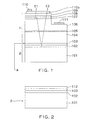
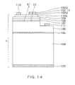
FIG. 1 is a schematic sectional view showing the first
preferred embodiment of a semiconductor white light emitting
device according to the present invention. A semiconductor light
emitting element 1 for emitting blue light El by current injection
and a semiconductor laminate 2 excited by the blue light E1 for
emitting yellow light E2 are bonded to each other at a bonding
surface A to constitute a semiconductor white light emitting
device. As can be seen from FIG. 1, these light beams are emitted
from the top side in the figure.
-
First, the semiconductor light emitting element 1 will be
described. On the top face of a sapphire substrate 104 in the
figure , there are sequentially formed a buffer layer 105, an
n-type GaN cladding layer (n-type contact layer) 106, an active
layer 107 having a GaN/InGaN multi-quantum well structure (MQW
structure), a p-type AlGaN cladding layer 108 and a p-type GaN
contact layer 109. Furthermore, the "n-type GaN cladding layer
106" will sometimes be referred to as the "n-type cladding layer
106" herein. The same applies to the other layers .
-
A part of the semiconductor light emitting element 1 is
etched to expose the n-type cladding layer 106 to form an n-side
electrode 111 contacting the n-type cladding layer 106. On
the top of the p-type contact layer 109, a p-side transparent
electrode 110a is formed. The p-side transparent electrode 110a
is made of a metal thin film or a conductive oxide film, and is
capable of transmitting blue light E1 emitted from the active
layer 107 and yellow light E2 emitted from a light emitting layer
102. Thus the transparent electrode is used, the emission
luminance of the device of FIG. 1 increases since the light
emitting surface is arranged on the p-type contact layer 109.
On the top of the p-side transparent electrode 110a, a p-side
electrode 110 is formed. A current is injected from the p-side
electrode 110 and the n-side electrode 111 to emit blue light
E1 from the active layer 107.
-
The semiconductor laminate 2 will be described below. The
semiconductor laminate 2 has a structure wherein the light
emitting layer 102 of an InAlP/InGaAlP multilayer film is located
between a GaAs substrate 101 and an InAlP cladding layer (contact
layer) 103. The GaAs substrate 101 has a lattice constant close
to that of the light emitting layer 102 of an InAlP/InGaAlP
multilayer film. Therefore, the GaAs substrate is used for
carrying out the crystal growth, the crystalline characteristic
of the light emitting layer 102 is improved to enhance the luminous
efficiency. The GaAs substrate 101 is non-transparent with
respect to yellow light E2 emitted from the light emitting layer
102 and blue light E1 emitted from the active layer 107. However,
since the GaAs substrate 101 is arranged on the opposite side
to the light emitting surface in the device of FIG. 1, the emission
luminance is high even if the GaAs substrate 101 exists. For that
reason, in the device of FIG. 1, the GaAs substrate is not removed,
so that the manufacturing process is simplified. Since the GaAs
substrate 101 also has a smaller band gap than the light emitting
layer 102, the GaAs substrate 102 does not serve as the cladding
layer of the light emitting layer 102. Therefore, in the
semiconductor laminate 2 of FIG. 1, the light emitting layer 102
is made of the InAlP/InGaAlP multilayer film, so that electrons
and holes generated by blue light E1 emitted from the
semiconductor light emitting element 1 can be confined in the
light emitting layer 102. Thus the light emitting layer 102 has
the multilayer structure, the luminous efficiency of the emitted
yellow light E2 is enhanced, so that the emission luminance of
the emitted yellow light E2 increases. In FIG.1 the top face of
the InAlP cladding layer 103 of the semiconductor laminate 2 thus
constructed is bonded to the bottom face of the sapphire substrate
104 of the semiconductor light emitting element 1.
-
In the semiconductor light emitting element 1 and
semiconductor laminate 2 described above, blue light E1 having
a wavelength of 485 nm is emitted from the active layer 107 of
the semiconductor light emitting element 1 by current injection,
a part of the blue light E1 emitted downward in the figure is
incident on the semiconductor laminate 2 , and the incident blue
light El excites the light emitting layer 102 of the semiconductor
laminate 2 to cause it to emit yellow light E2 having a wavelength
of 590 nm. Thus, the blue light E1 emitted from the active layer
107 and the yellow light E2 emitted from the light emitting layer
102 can realize white light emission.
-
In the semiconductor white light emitting device of FIG.
1, the color temperature of white light was about 8000 K, and
the luminous intensity during the injection of a current of 20
mA is 2 cd in a package having a radiation angle of 10 degrees.
The color temperature of white light can be controlled by
adjusting the emission wavelengths and emission intensities of
the semiconductor light emitting element 1 and semiconductor
laminate 2. In the element structure of FIG. 1, the transparent
characteristic of the p-side transparent electrode 110a also has
an influence on the color temperature and the luminous intensity.
That is, since the p-side transparent electrode 110a transmits
light E1 and light E2 having different wavelengths, a required
color temperature can be obtained by adjusting the transmittance
for each light.
-
In the semiconductor white light emitting device of FIG.
1 described above, it is possible to decrease the variation in
tone for each element. Because the thickness and composition of
the semiconductor laminate 2 hardly vary for each element. That
is, by using a standardized mass production process generally
used for the manufacturing of semiconductor elements, the
semiconductor laminate 2 can be manufactured with high
repeatability so that the thickness and composition hardly vary.
Thus the thickness and composition of the semiconductor laminate
2 are uniform for each element, the ratio of the quantity of the
blue light E1 emitted from the semiconductor light emitting
element 1 to that of the yellow light E2 emitted from the
semiconductor laminate 2 does not vary for each device , so that
the tone does not vary for each device.
-
In the semiconductor white light emitting device of FIG.
1, the tone hardly deteriorates with age , because the
deterioration with age of the yellow light emitting semiconductor
laminate 2 is smaller than that of fluorescent lamps. Since the
deterioration with age of the semiconductor laminate 2 is small ,
the ratio of the quantity of the blue light E1 emitted from the
semiconductor light emitting element 1 to that of the yellow light
E2 emitted from the semiconductor laminate 2 does not vary, so
that the tone hardly vary.
-
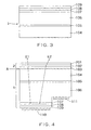
Referring to FIGS. 2 and 3, a method for manufacturing the
semiconductor white light emitting device of FIG. 1 will be
described below. As shown in FIG. 2, one of the features of this
manufacturing method is that a light emitting layer 103 is formed
on a GaAs substrate 101 suitable for the formation of the light
emitting layer 103, and thereafter, this is bonded to a
semiconductor blue light emitting device 1.
-
First, in the manufacturing of the
semiconductor laminate
2, a GaAs substrate (a second substrate) 101 is cleaned with an
organic solvent and/or a sulfuric acid containing etchant, and
then, the
GaAs substrate 101 is introduced into an MOCVD system.
Then, the
GaAs substrate 101 is heated to 730°C, and an appropriate
5-Group material serving as a P material is supplied to
sequentially grow a
light emitting layer 102 of an InAlP/InGaAlP
multilayer film and an
InAlP cladding layer 103. Further a
GaAs
cap layer 112 is grown on the surface thereof. The
GaAs cap layer
112 is a protection layer which is finally removed. The thickness
of these layers are shown in the following table 1.
| InAlP/InGaAlP Light Emitting Layer 102 | 30 nm / 50 nm |
| InAlP Cladding Layer 103 | 300 nm or less |
| GaAs Cap Layer 113 | 100 nm |
-
Specifically, the light emitting layer 102 has a structure
wherein 20 InAlP layers having a thickness of 30 nm and 20
In0.5(Ga0.7Al0.3)0.5P layers having a thickness of 50 nm are
alternately stacked. The InAlP cladding layer 103 serves as an
adhesive layer for bonding the semiconductor laminate 2 to the
semiconductor light emitting element 1, also serves and as a
protection layer for protecting the light emitting layer 102.
At the same time it has the function of confining excitation
carriers therein. Since the InGaAlP contact layer absorbs
emitted blue light E1, it preferably has a thickness of 100 nm
or less to reduce light loss due to the absorption of blue light
E1.
-
Then, in the manufacturing of the semiconductor
light
emitting element 1, as can be seen from FIG. 3, a sapphire
substrate (a first substrate) 104 is cleaned with an organic
solvent and/or a sulfuric acid containing etchant, and then, is
introduced into the MOCVD system. Then, after the
sapphire
substrate 104 is thermally cleaned at 1100 °C, a
buffer layer 105,
an n-type
GaN cladding layer 106, a GaN/InGaN
active layer 107
of the MQW structure, a p-type
AlGaN cladding layer 108 and a
p-type
GaN cladding layer 109 are sequentially formed. The
growth temperature and thickness of these layers are shown in
Table 2.
| Buffer Layer 105 | 500 °C | 30 nm |
| n-type GaN Cladding Layer 106 | 1050 °C | 4 µm |
| GaN/InGaN Active Layer 107 | 750 °C | 7 nm / 3 nm |
| p-type AlGaN Cladding Layer 108 | 1050 °C | 50 nm |
| p-type GaN Contact Layer 109 | 1050 °C | 150 nm |
-
Specifically, the active layer 107 has a 5QW structure of
an In0.35Ga0.65N layer having a thickness of 3 nm and a GaN layer
having a thickness of 7 nm.
-
Then, the semiconductor light emitting element 1 and the
semiconductor laminate 2 thus manufactured are bonded to each
other. Before bonding, the GaAs cap layer 112 formed on the
semiconductor laminate 2 as the protection layer is etched to
be removed with a sulfuric acid containing etchant. After the
GaAs cap layer 112 is removed, the surface of the InAlP cladding
layer 103 is subsequently cleaned. With respect to the
semiconductor light emitting element 1, the bottom side of the
sapphire substrate 104 in FIG. 3 is mirror-polished and
simultaneously trimmed to form a flat surface. In order to
facilitate the element isolation which will be carried out later,
the trimming was carried out so that the whole thickness of the
semiconductor light emitting element 1 is about 100 µm.
-
Then, the bottom side of the sapphire substrate 104 of the
semiconductor light emitting element 1 in FIG. 3 is aligned with
the top side of the InAlP cladding layer 103 of the semiconductor
laminate 2 in FIG. 2. Specifically, after the semiconductor
light emitting element 1 is aligned with the semiconductor
laminate 2, they are annealed at 500°C in an atmosphere of nitrogen
for 30 minutes to be bonded to each other by a dehydrating
condensation reaction. In order to improve adhesion, the
surfaces to be bonded are preferably as flat as possible. In the
planarization of the InAlP cladding layer 103 of the semiconductor
laminate 2, the GaAs substrate 101 inclined in a direction of
[011] from the plane (100) is effectively used. In FIG. 2, the
GaAs substrate 101 inclined at 15° is used so that the surface
roughness of the top side of the InAlP cladding layer 103 in the
figure is about 2 nm. The surface roughness of the bottom side
of the sapphire substrate 104 in FIG. 3 is made 20 nm or less
by the mirror polishing.
-
Then, as can be seen from FIG. 1, a part of the semiconductor
light emitting element 1 is etched from the p-type contact layer
109 to the n-type cladding layer 106, and then, n-side electrode
111 , a p-side transparent electrode 110a and a p-side electrode
110 are formed on the exposed n-type cladding layer 106 and p-type
contact layer 109. Moreover, the bottom side of the GaAs
substrate 101 is polished if necessary.
-
The semiconductor white light emitting device of FIG. 1
is thus obtained.
-
In the above described method for manufacturing the
semiconductor light emitting device in this preferred embodiment,
the light emitting layer 102 is formed on the top of the GaAs
substrate 101 suitable for the formation of the light emitting
layer 102, and, this is bonded to the semiconductor blue light
emitting element 1. Therefore it is possible to provide a
semiconductor white light emitting device which has a small number
of crystal defects in the light emitting layer 102 and which has
high reliability.
-
In the method for manufacturing the semiconductor light
emitting element in this preferred embodiment, the blue light
emitting semiconductor light emitting element 1 and the yellow
light emitting semiconductor laminate 2 are integrated with each
other by bonding to fabricate a single device. Therefore, the
device can be used in a space smaller than it is used to be in
a case where two devices are used, and the number of electrodes
can be reduced. In addition, since the device can be regard as
a point light source by the integration, it is possible to provide
an element showing a small variation in emitting lights.
(Second Preferred Embodiment)
-
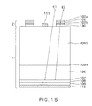
As can be seen from FIG. 4, one of different points of a
semiconductor white light emitting device in the second preferred
embodiment from the device in the first preferred embodiment (FIG.
1) is that the substrate 104 side of a semiconductor light emitting
element 1 serves as a light emitting surface and that a
semiconductor laminate 2 is bonded to the side of the light
emitting surface.
-
FIG. 4 is a schematic sectional view showing the second
preferred embodiment of a semiconductor white light emitting
device according to the present invention. The same reference
numbers are given to elements corresponding to those in the first
preferred embodiment (FIG. 1). As in the case with the first
preferred embodiment (FIG. 1), a semiconductor light emitting
element 1 for emitting blue light E1 from an active layer 107
by current injection and a semiconductor laminate 2 excited by
the blue light E1 for emitting yellow light E2 from a light
emitting layer 102 are bonded to each other at a bonding surface
A to constitute a semiconductor white light emitting device. As
can be seen from FIG. 4, these light beams are emitted from the
top side in the figure.
-
First, the semiconductor light emitting element 1 will be
described. One of different points of the semiconductor light
emitting element 1 from that in the first preferred embodiment
(FIG. 1) is that the transparent electrode 110a is not used as
a p-side electrode. In the semiconductor light emitting element
1 of FIG. 4, a p-side electrode 110 of Ni/Au or the like having
a high reflectance is formed substantially on the entire surface
of a p-type contact layer 109. Thus, the blue light E1 emitted
downward from the active layer 107 in the figure can be reflected
on the p-side electrode 110 to be effectively emitted from the
light emitting surface on the top side in the figure. Other
principal features are the same as those in the first preferred
embodiment.
-
The semiconductor laminate 2 will be described below. One
of different points of the semiconductor laminate 2 from that
in the first preferred embodiment (FIG. 1) is that the GaAs
substrate 101 is removed and an SiO2 protection layer 201 is formed
on that surface. This is for preventing light from being absorbed
into the GaAs substrate 101. That is, in the device of FIG. 4,
the semiconductor laminate 2 is bonded to the light emitting
surface. Accordingly if the GaAs substrate exists, the emitted
blue light E1 and yellow light E2 are absorbed into the GaAs
substrate if the GaAs substrate exists. Therefore, the GaAs
substrate is removed to enhance the emission luminance.
-
A process for manufacturing the semiconductor light
emitting element 1 and the semiconductor laminate 2 is basically
the same as that in the first preferred embodiment. Specifically,
the InAlP/InGaAlP multilayer film 102 is formed so as to have
a structure that 10 InAlP layers and 10 In0.5(Ga0.7Al0.3)0.5P layers
are alternately stacked. The GaAs substrate is removed with a
hydrofluoric acid containing etchant.
-
The semiconductor white light emitting device of FIG. 4
thus obtained was mounted on a package so that the electrodes
110 and 111 faced downward, and a current was injected. As a
result, the blue light E1 having a wavelength of 485 nm was emitted
from the active layer 107, and the yellow light E2 having a
wavelength of 590 nm was emitted from the light emitting layer
102 by exciting the blue light E1. These light beams passed
through the oxide film 201 to be observed as white light. The
color temperature of white light was about 8000 K, and the luminous
intensity during the injection of a current of 20 mA was 3cd in
a package having a radiation angle of 10 degrees.
-
Even if the light emitting surface is arranged on the side
of the substrate 104 as in this preferred embodiment, it is
possible to decrease the variation in tone in each device and
the variation in tone due to deterioration with age, as in the
case with the first preferred embodiment.
(Third Preferred Embodiment)
-
As can be seen from FIG. 5, one of different points of a
semiconductor white light emitting device in the third preferred
embodiment from the device in the second preferred embodiment
(FIG. 4) is that two light emitting layers 302 and 304 are formed
in a semiconductor laminate 2.
-
FIG. 5 is a schematic sectional view showing the third
preferred embodiment of a semiconductor white light emitting
device according to the present invention. The same reference
numbers are given to elements corresponding to those in the second
preferred embodiment (FIG. 4). A semiconductor light emitting
element 1 for emitting blue light E1 from an active layer 107
by current injection and a semiconductor laminate 2, which is
excited by the blue light E1 for emitting green light E2 from
a first light emitting layer 304 and which is excited by the green
light E2 and the blue light E1 for emitting red light E3 from
a second light emitting layer 302, constitute a semiconductor
white light emitting device. As can be seen from FIG. 5, these
light beams are emitted from the top side in the figure.
-
First, the structure of the semiconductor light emitting
element 1 is basically the same as that in the second preferred
embodiment (FIG. 4), so that the detailed description thereof
is omitted.
-
The semiconductor laminate 2 will be described below.
Between the first light emitting layer 304 and the second light
emitting layer 302, a first InAlP cladding layer 303 is provided.
On the bottom face of the first light emitting layer 304 in the
figure, a second InAlP cladding layer 305 for bonding the
semiconductor laminate 2 to the semiconductor light emitting
element 1 is formed. The top face of the second light emitting
layer 302 in the figure is covered with an oxide film 306 which
is a protection layer.
-
When a third InAlP cladding layer (not shown) is provided
between the oxide film 306 and the second light emitting layer
302, it is possible to adjust tone. That is, when the third InAlP
cladding layer is provided, carriers are effectively confined
in the second light emitting layer 302, so that the quantity of
red light E3 increases, and the blue light E1 is absorbed into
the third InAlP cladding layer, so that the quantity of blue light
E1 decreases.
-
As shown in FIG. 5, in the above described semiconductor
light emitting element 1 and semiconductor laminate 2, the side
of the protection layer 306 of the semiconductor laminate 2 serves
as a light emitting surface to obtain white color due to the color
mixture of three emissions E1, E2 and E3. That is, the current
is injected into the semiconductor light emitting element 1 to
obtain the blue light E1 emitted from the active layer107 having
the MQW structure, and the first light emitting layer 304 of the
semiconductor laminate 2 is excited to obtain the green light
2. Moreover, the second light emitting layer 302 is excited with
the emitted blue light E1 and green light E2 to obtain the red
light E3. By the hybridization of these light beams, white light
is obtained.
-
Specifically, blue light E1 having a wavelength of 485 nm
was emitted from the MQW layer 107, green light E2 having a
wavelength of 565 nm was emitted from the first light emitting
layer 304, and red light E3 having a wavelength of 620 nm was
emitted from the second light emitting layer 302, so that white
light was observed by the color mixture. The color temperature
of white light was about 6500 K. The luminous intensity during
the injection of a current of 20 mA was 2 cd in a package having
a radiation angle of 10 degrees.
-
Even in the case of the semiconductor white light emitting
device for obtaining white light by the color mixture of blue
light E1, green light E2 and red light E3, it is possible to reduce
the variation in tone in each device and the variation in tone
due to deterioration with age, as in the case with the first
preferred embodiment.
-
In the device of FIG. 5, the blue light E1 is emitted by
the current injection, whereas the green light E2 and the red
light E3 are emitted by optical pumping. Therefore, the variation
in tone in each device due to the lost balance of current injection
doe not occur. For example, in a case where a current is injected
into each of the blue light emitting active layer ,the green light
emitting active layer and the red light emitting active layer
to obtain white light, when the quantity of the current injected
into the blue light emitting active layer increases due to the
lost balance of current injection, the tone is caused to near
to blue. However, in the device of FIG. 5, such a variation in
tone in each device does not occur.
-
Referring to FIG. 6, a method for manufacturing the
semiconductor white light emitting device of FIG. 5 will be
described below. As shown in FIG. 6, one of the features of this
manufacturing method is that a first light emitting layer 304
and a second light emitting layer 302 are formed on a GaAs
substrate 301 suitable for the formation of the light emitting
layers 304 and 302, and thereafter, this is bonded to a
semiconductor light emitting device 1.
-
FIG. 6 shows the structure of the semiconductor laminate
2 in the second preferred embodiment before the bonding. This
will be specifically described in accordance with manufacturing
steps.
-
First, a GaAs substrate 301 is cleaned with an organic
solvent and/or a sulfuric acid containing etchant, and then, the
substrate is introduced into an MOCVD system. Then, the
substrate is heated to 730°C, and an appropriate 5-Group material
serving as a P material is supplied to sequentially crystal-grow
a second light emitting layer 302 of an InAlP/InGaAlP
multilayer film, a first InAlP cladding layer 303, a first light
emitting layer 304 of an InAlP/InGaAlP multilayer film, and a
second InAlP cladding layer 305 to further grow a GaAs cap layer
307 on the surface thereof to obtain a stacked structure shown
in FIG. 6. The GaAs cap layer 307 is a protection layer which
is ultimately removed.
-
The thickness of these crystalline layers are shown in
Table 3.
| InAlP/InGaAlP Light Emitting Layer 302 | 30 nm / 50 nm |
| InAlP Cladding Layer 303 | 500 nm or less |
| InAlP/InGaAlP Light Emitting Layer 304 | 30 nm / 50 nm |
| InAlP Cladding Layer 305 | 300 nm or less |
| GaAs Cap Layer 307 | 100 nm |
-
Specifically, the second light emitting layer 302 has a
structure wherein 20 InAlP layers having a thickness of 30 nm
and 20 In0.5(Ga0.8Al0.2)0.5P layers having a thickness of 50 nm are
alternately stacked. The first light emitting layer 304 has a
structure wherein 20 InAlP layers having a thickness of 30 nm
and 20 In0.5(Ga0.6Al0.4)0.5P layers having a thickness of 50 nm are
alternately stacked. The InAlP contact layer 305 serves both as
an adhesive layer for bonding the semiconductor laminate 2 to
the semiconductor light emitting element 1 and as a protection
layer for protecting the light emitting layer 304, and at the
same time ,also have the function of confining light in the light
emitting layer 304.
-
Then, the cap layer 307 of the semiconductor laminate 2
thus manufactured is removed, and the semiconductor laminate 2
is bonded to the semiconductor light emitting element 1 as in
the case with the first preferred embodiment. Then, the GaAs
substrate 301 is etched to be removed, and a protection layer
306 is formed on the surface thus etched, so that the device
structure of FIG. 5 is obtained.
-
In the above described method for manufacturing the
semiconductor light emitting device of FIG. 5, as in the case
with the first preferred embodiment, the light emitting layers
302 and 304 are formed on the top of the GaAs substrate 301 suitable
for the formation of the light emitting layers 302 and 304, and
thereafter, this is bonded to the semiconductor blue light
emitting element 1, so that it is possible to provide a
semiconductor white light emitting device which has a small number
of crystal defects in the light emitting layers 302 and 304 and
which thus has high reliability.
-
In the method for manufacturing the device wherein the
semiconductor laminate 2 is provided on the side of the light
emitting surface ,as shown in FIG. 5, it is possible to prevent
light from being absorbed into the GaAs substrate 301 by etching
and removing the GaAs substrate 301, so that it is possible to
enhance the emission luminance of the device.
-
In the method for manufacturing the semiconductor light
emitting device of FIG. 5, the semiconductor light emitting
element 1 for emitting blue light E1 and the semiconductor
laminate 2 for emitting green light E2 and red light E3 are
integrated with each other by bonding to fabricate a single device.
Therefore, the device can be used in a smaller space than that
in a case where two or three devices are used, and the number
of electrodes can be reduced. In addition, since the device can
be regarded as a point light source by the integration, it is
possible to provide a device having a small variation in emission.
(Fourth Preferred Embodiment)
-
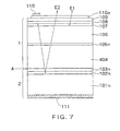
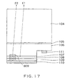
As can be seen from FIG. 7, one of different points of a
semiconductor white light emitting device in the fourth preferred
embodiment from the device in the first preferred embodiment (FIG.
1) is that an n-type semiconductor substrate 404 such as an n-type
GaN, n-type SiC, n-type Si substrate is used as the substrate
of a semiconductor light emitting element 1 , and that an n-type
electrode 111 is formed on the reverse surface of the
substrate 101n of a semiconductor laminate 2. In the device of
FIG. 7, a current is injected from the n-side electrode 111 into
an active layer 107 via an n-type GaAs substrate 101n, a light
emitting layer 102n of an n-type InAlP/InGaAlP multilayer film,
an n-type InAlP cladding layer 103n, an n-type semiconductor
substrate 404, an n-type AlGaN buffer layer 105n and a GaN contact
layer 106. Other principal structures are the same as those in
the first preferred embodiment.
-
Even in the case of the semiconductor light emitting device
wherein the electrodes are provided on the top and bottom as shown
in FIG. 7, it is possible to reduce the variation in tone in each
device and the variation in tone due to deterioration with age,
as in the case with the first preferred embodiment.
-
Even in the case of the device of FIG. 7, it is possible
to use a manufacturing method which is substantially the same
as that in the first preferred embodiment (FIG. 1), and it is
possible to obtain a device having high reliability , as in the
case with the first preferred embodiment. Moreover, in the case
of the device of FIG. 7, an etching step of forming an n-side
electrode is not required to carry out, so that the manufacturing
method is simplified.
(Fifth Preferred Embodiment)
-
As can be seen from FIG. 8, one of different points of a
semiconductor white light emitting device in the fifth preferred
embodiment from the device in the first preferred embodiment (FIG.
1) is that the non-transparent GaAs substrate 101 of a
semiconductor laminate 2 is etched to be removed and that another
transparent substrate 501 is bonded to a bonding surface A2.
Specifically, a GaP substrate or ZnSe substrate for transmitting
yellow light is used as the transparent substrate 501. Other
principal structures are the same as those in the first preferred
embodiment. Furthermore, the bonding surface A in the first
preferred embodiment (FIG. 1) corresponds to the bonding surface
A1 in the fifth preferred embodiment (FIG. 8).
-
In the device of FIG. 8, yellow light E2s emitted from an
InAlP/InGaAlP light emitting layer 102 can also be emitted from
the side of the newly bonded substrate 501 as shown by a broken
line. Therefore, if, for example, when the inner wall surface
of a package is formed as a recessed surface to emit the radiation
E2s upward, the radiation E2s can be effectively utilized.
-
In the above described first through fifth preferred
embodiments, an InAlP layer 103 was used as a cladding layer (also
serving as a contact layer) for bonding the light emitting layer
102 of a semiconductor laminate 2 to a semiconductor light
emitting element 1. On the top of the InAlP cladding layer 103,
a cladding layer of another material may be formed in place of
the cladding layer 103. Such a cladding layer may be made of,
e.g., GaN or Gap. By providing such a cladding layer, the light
confining effect in a multilayer film 102 can be enhanced. A GaN
cladding layer is particularly preferable since it transmits blue
light, though it is a polycrystalline thin film. In accordance
with the material of a substrate to be bonded, GaAlAs or InGaAlP
may be used.
-
Although etching and/or polishing was used as a pretreatment
before bonding, gas etching or thermal cleaning in
various amorphous gases may be carried out. Moreover, the
annealing atmosphere and temperature can be suitably changed.
When a high annealing temperature is used, an atmosphere gas may
be selected to apply a suitable pressure in order to prevent atoms
from being emitted and removed from crystal.
-
For bonding, an adhesive may be used. For example, if an
adhesive is used in the device in the fifth preferred embodiment
(FIG. 5), setting the refractive index of the adhesive to be at
a value between the refractive index of the sapphire substrate
104 and the refractive index of the InAlP cladding layer, enables
the reduction in quantities of blue light E1 and yellow light
E2 reflected on the bonding surface Al, so that it is possible
to enhance the emission luminance of the device.
(Sixth Preferred Embodiment)
-
FIG. 9 is a schematic sectional view of the sixth preferred
embodiment of a semiconductor white light emitting device
according to the present invention. Unlike the preceding
preferred embodiments wherein the semiconductor light emitting
device is bonded to the semiconductor laminate, a light emitting
layer 702 and an active layer 706 in this preferred embodiment,
are formed on an n-type GaAs substrate 701 by crystal growth.
That is, on the n-type GaAs substrate 701, there are sequentially
stacked an n-type InAlP/InGaAlP light emitting layer 702 for
emitting yellow light E2 by optical pumping, an n-type ZnSe buffer
layer 703, an n-type ZnMgSSe cladding layer 704, an n-type ZnSe
optical guiding layer 705, a ZnSe/ZnCdSe MQW active layer 706
for emitting blue light E1 by current injection, a p-type ZnSe
optical guiding layer 707, a p-type ZnMgSSe cladding layer 708,
and a p-type ZnTe/ZnSe superlattice contact layer 709. On the
p-type contact layer 709, a p-side transparent electrode 710a
and a p-side electrode 710 are formed, and on the n-type GaAs
substrate 701, an n-side electrode 711 is formed.
-
For the crystal growth of the device of FIG. 9, the MOCVD
method and the MBE method are combined. That is, the MOCVD method
is used for the crystal growth of the n-type InAlP/InGaAlP light
emitting layer 702 on the n-type GaAs substrate 701, and the MBE
method was used for the growth of the n-type ZnSe buffer layer
703 to the p-type ZnTe/ZnSe superlattice contact layer 709 thereon.
This is because a good conductive type control can be achieved
by using the MBE method particularly for ZnSe compound p-type
conductive layers.
-
In the semiconductor white light emitting device thus
formed, blue light E1 is emitted from the active layer 706 by
passing a current between the electrodes 710 and 711. A part of
the blue light E1 passes through the element to be absorbed into
the light emitting layer 702 to excite yellow light E2. This
yellow light E2 is emitted from the top side in the figure. By
the hybridization of the blue light E1 and yellow light E2, white
light is obtained.
-
In fact, white light was observed by the color mixture of
blue light E1 having a wavelength of 485 nm and yellow light E2
having a wavelength of 590 nm. The color temperature of the white
light was about 8000 K, and the luminous intensity during the
injection of a current of 20 mA was 2 cd in a package having a
radiation angle of 10 degrees.
-
Even in the case of the above described semiconductor light
emitting device of FIG. 9 using the ZnSe compound semiconductor
light emitting element 1, it is possible to reduce the variation
in tone in each device and the variation in tone due to
deterioration with age, as in the case with the first preferred
embodiment.
-
A method for manufacturing the device of FIG. 9 will be
briefly described below. First, an n-type GaAs substrate 701 is
cleaned with an organic solvent and/or a sulfuric acid containing
etchant, and then, the substrate is introduced into an MOCVD
system. Then, the substrate is heated to 730 °C , and an
appropriate 5-Group material serving as a P material is supplied
to grow an n-type InAlP/InGaAlP light emitting layer 702. Then,
the substrate is transferred to an MBE system to grow thereon
an n-type ZnSe buffer layer 703 to a p-type ZnTe/ZnSe superlattice
contact layer 709. Specifically, the n-type InAlP/InGaAlP light
emitting layer 702 was formed so as to have a structure wherein
20 InAlP layers and 20 In0.5(Ga0.7Al0.3)0.5P layers are alternately
stacked.
-
As described above, in the semiconductor light emitting
device of FIG. 9, the n-type InAlP/InGaAlP light emitting layer
702 and the ZnSe/ZnCdSe MQW active layer 706 are formed on the
n-type GaAs substrate 701 by crystal growth, so that it is possible
to simplify the manufacturing process.
-
In addition, since the lattice constant of the ZnSe
compound semiconductor is close to the lattice constant of the
GaAs compound semiconductor, even if the above described crystal
growth is carried out, it is possible to provid a semiconductor
white light emitting device which has a small number of crystal
defects and which has high reliability.
(Seventh Preferred Embodiment)
-
As can be seen from FIG. 10, one of different points of
a semiconductor white light emitting device in the seventh
preferred embodiment from the device in the sixth preferred
embodiment (FIG. 9) is that etching is carried out from the side
of a p-type contact layer 709 to expose an n-type buffer layer
703 and that an n-side electrode 711 is formed on the n-type buffer
layer 703. Other principal constructions are the same as those
in the sixth preferred embodiment.
-
Even in the case of the device of FIG. 10, it is possible
to obtain white light by color mixture as in the case with the
sixth preferred embodiment, so that it is possible to obtain the
same advantages as those in the sixth preferred embodiment.
-
while the InGaAlP materials semiconductors and the ZnSe
compound semiconductors have been crystal-grown by the MOCVD
method and the MBE method, respectively, in the sixth and seventh
preferred embodiments, both may be crystal-grown by the MBE method.
Also in the case of the material system in the sixth and seventh
preferred embodiments, two light emitting layers may be formed
on separate element substrates, respectively, to bond and
integrate the substrates with each other as in the case with the
first preferred embodiment.
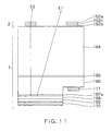
(Eighth Preferred Embodiment)
-
In the following eighth through eleventh preferred
embodiments, there will be described a device wherein a
semiconductor laminate 2 having a double-hetero structure is
bonded to a part of a light emitting surface of a GaN compound
semiconductor light emitting element 1 or a part of the opposite
surface thereto, as shown in, e.g., FIG. 11. Furthermore, in the
following preferred embodiments, the detailed description of the
manufacturing process is omitted.
-
FIG. 11 is a schematic sectional view showing the eighth
preferred embodiment of a semiconductor white light emitting
device according to the present invention. The same reference
numbers are given to elements corresponding to those in the first
preferred embodiment (FIG. 1). A semiconductor white light
emitting device comprises a semiconductor light emitting element
1 for emitting blue light E1 by current injection, and a
semiconductor laminate 2 excited by the blue light E1 for emitting
yellow light E2. As can be seen from FIG. 12, these light beams
are emitted from the top side in the figure.
-
First, the semiconductor light emitting element 1 will be
described. On the bottom face of a sapphire substrate 104 in the
figure, there are sequentially formed a buffer layer 105, an
n-type GaN cladding layer 106, an InGaAlN active layer 107a, a
p-type AlGaN cladding layer 108 and a p-type GaN contact layer
109. Although the thickness of each of the layers 104 to 109 is
several µm and the thickness of the sapphire substrate 104 is
hundreds µm, the scale factor thereof is changed in FIG. 11 for
the purpose of easier explanation of the stacked layers 104
through 109.
-
The wavelength of light emitted from the above described
InGaAlN active layer 107 is designed to emit blue light E1 by
controlling the composition ratio of In and Al of the active layer.
The composition ratio of Al may be 0 so that the active layer
is made of InGaN. If this active layer 107a has a single-quantum
well or multi-quantum well structure of a thin film having a
thickness of about 1 nm to 10 nm, it is possible to realize high
luminance. A current is injected into the active layer 107a from
an n-side electrode 111, which is formed on the n-type cladding
layer 106, and from a p-side electrode 110 which is formed on
the p-type contact layer 109. The p-side electrode 110 and the
n-side electrode 111 are preferably made of Ni/Au and Ti/Al,
respectively, which are materials having a high reflectance for
reflecting blue light emitted from the active layer 107a. Thus,
the blue light E1 emitted from the active layer 107a downward
in the figure can be reflected on the p-side electrode 110 and
the n-side electrode 111 to be emitted from the light emitting
surface on the top side in the figure. Furthermore, the portions
shown by slant lines in the figure, such as the p-side electrode
110 and the n-side electrode 111, are the portions having the
property of reflecting the blue light E1 and the yellow light
E2.
-
The semiconductor laminate 2 will be described below. The
semiconductor laminate 2 has a structure wherein an InGaAlP light
emitting layer 102c is located between a p-type InGaAlP cladding
layer 102b and an n-type InGaAlP cladding layer 102a. The light
emitting layer 102c is designed to emit the yellow light E2 by
controlling the composition ratio of 3-Group elements, In, Ga
and Al, of InGaAlP. The thickness of the light emitting layer
102 is preferably in the range of from 1 nm to 10 µm. That is,
when the light emitting layer 102c has a single-quantum well or
multi-quantum well structure of a thin film having a thickness
of one nm to tens nm, the luminous efficiency of yellow light
increases to increase the intensity of yellow light, and when
the light emitting layer 102c is made of a single layer or
multilayer film having a thickness of tens nm to 10 µm, the
absorption efficiency of blue light increases to increase the
intensity of yellow light. The two cladding layers 102a and 102b
on both sides of the light emitting layer 102c have a greater
band gap than the light emitting layer 102c. That is, the
semiconductor laminate 2 has a double-hetero structure. Because
of the double-hetero structure, electrons and holes generated
by the blue light E1 emitted from the semiconductor light emitting
element 1 can be effectively confined in the light emitting layer
102c, so that the luminous efficiency of the yellow light E2 can
increase to increase the emission luminance of the yellow light
E2. Also, because of the double-hetero structure, the emission
luminance of the yellow light E2 increases even if the light
emitting layer 102c is made of a single layer film. If the
cladding layers for locating the light emitting layer 102c are
p-type and n-type cladding layers as in this preferred embodiment,
the intensity of the yellow light E2 of the light emitting layer
102c further increases. This results was obtained by the
inventors' experiment. It is analyzed that the reason for this
is that the absorption efficiency is increased by the internal
field. No element may be doped into the cladding layers 102a and
102b. In the case of such undoping, the crystalline
characteristics of the light emitting layer 102c are improved,
i.e., the non-emission center of the light emitting layer 102
decreases, and the intensity of the yellow light E2 in the light
emitting layer 102c increases.
-
When the semiconductor laminate 2 having the double-hetero
structure is used as in the device of FIG. 11, the area of the
semiconductor laminate 2 is preferably set to be 1/3 to 2/3 of
the area of the sapphire substrate 104 on the top side in the
figure. That is, as described above, when the semiconductor
laminate 2 has the double-hetero structure, the intensity of the
yellow light E2 increases. However, if the double-hetero
structure is used, the n-type cladding layer 102a absorbs the
blue light E1, so that the intensity of the blue light E1 decreases.
Therefore, when the semiconductor laminate 2 is the double-hetero
structure and when the area of the semiconductor laminate 2 has
the same as that on the top side in the figure, the intensity
of the yellow light E2 is too strong, so that the tone of white
light is caused to approach yellow. Therefore, if the area of
the semiconductor laminate 2 is set to be 1/3 to 2/3 of the area
of the sapphire substrate, it is possible to obtain white light
having a good balance.
-
The thickness of the above described p-type cladding layer
102b is preferably 300 nm or less, and more preferably 100 nm
or less. The reason for this is that the quantity of blue light
E1 for exciting the light emitting layer 102c decreases when the
p-type cladding layer 102b is too thick since the p-type cladding
layer 102b has the property of absorbing blue light E1. On the
other hand, since the n-type cladding layer 102a has the property
of transmitting yellow light E2, its thickness may be increased
if necessary.
-
As shown in FIG. 11, the semiconductor laminate 2 is bonded
to a part of the top side of the sapphire substrate 104 of the
semiconductor light emitting element 1 in the figure. For
example, this semiconductor laminate 2 may be formed by
sequentially forming the n-type cladding layer 102a, the light
emitting layer 102c and the p-type cladding layer 102b on the
GaAs substrate, heat-treating the substrate at a temperature of
460 °C to 750°C in an atmosphere of an inert gas, bonding the p-type
cladding layer 102b on the top side of the sapphire substrate
104 in the figure, and etching and removing the GaAs substrate.
-
In the above described semiconductor light emitting
element 1 and semiconductor laminate 2, blue light E1 is emitted
from the active layer 104 of the semiconductor light emitting
element 1, and a part of the blue light E1 is incident on the
semiconductor laminate 2. The incident blue light E1 excites the
light emitting layer 102c of the semiconductor laminate 2, so
that yellow light E2 is emitted from the light emitting layer
102. Thus, the blue light E1 emitted from the active layer 107
and the yellow light E2 emitted from the light emitting layer
102c are mixed to realize white light.
-
Referring to the chromaticity diagram of FIG. 12, this
white light will be described below in detail. FIG. 12 is an xy
chromaticity diagram defined by International Commission on
Illumination (CIE). The emission wavelength of an InGaAlN active
layer, such as the active layer 107a of the semiconductor light
emitting element 1 of FIG. 11, can be in the range of from 380
nm to 500 nm as shown on the left side of FIG. 12. The emission
wavelength of an InGaAlP light emitting layer, such as the light
emitting layer 102c of the semiconductor laminate 2, can be in
the range of from 540 nm to 750 nm as shown on the right side
of FIG. 12. If for example, the color mixture of blue light having
a wavelength of 476 nm emitted from the InGaAlN active layer with
yellow light having a wavelength of 578 nm emitted from the InGaAlP
light emitting layer is intended to be carried out, a straight
line drawn between a white circle of 476 in the lower-left blue
region and a white circle of 578 in the upper-right yellow region
is considered. Then, it can be seen that this straight line passes
through a white region. It can thus be seen from FIG. 12 that
white light can be realized by the color mixture of the blue light
emitted from the semiconductor light emitting element 1 and the
yellow light E2 emitted from the semiconductor laminate 2.
-
Similarly, it can be seen from FIG. 12 that white light
can be realized by the color mixture of bluish green light with
red light when the emission wavelength of the InGaAlN active layer
107a is set to be 495 nm and the emission wavelength of the InGaAlP
light emitting layer 102c is set to be 750 nm.
-
In the above described semiconductor of FIG. 11, it is
possible to decrease the variation in tone in each device. This
is because unlike fluorescent material, the thickness,
composition, and other characteristics and area of the
semiconductor laminate 2 hardly vary in each element. That is,
by using a standardized mass production process generally used
for the manufacturing of semiconductor elements, the
semiconductor laminate 2 can be manufactured with high
repeatability so that the thickness, composition and other
characteristics hardly vary, and can be easily worked so as to
have the same area. Then, when the thickness, composition, and
other characteristics and area of the semiconductor laminate 2
are uniform for each element, the ratio of the blue light E1
emitted from the semiconductor light emitting element 1 to the
yellow light E2 emitted from the semiconductor laminate 2 does
not vary for each element, so that the tone does not vary for
each element.
-
In the semiconductor light emitting device of FIG. 11, the
tone can also be adjusted by changing the area of the semiconductor
laminate 2. Because of this, when the luminous efficiency of the
semiconductor laminate 2 varies for some reason or other, for
example, the tone can be adjusted. In a simple manner, the
luminous efficiency of the semiconductor laminate 2 decreases,
the area of the semiconductor laminate may be increased.
-
Also, it is necessary to change the tone of white light
is intended, the tone can be easily changed by changing the area
of the semiconductor laminate 2 as described above. For example,
when an element for emitting white light having a tone close to
blue is intended to be manufactured as a displaying element, the
area of the semiconductor laminate 2 for emitting yellow light
may be decreased.
-
Moreover, in the semiconductor light emitting device of
FIG. 11, it is possible to further improve the emission luminance
than that in conventional elements. That is, since the
semiconductor laminate 2 is formed only on a part of the light
emitting surface in the element of FIG. 11, it is possible to
utilize blue light which does not pass through the semiconductor
laminate 2 serving as a wavelength converting region, i.e., blue
light having a high luminance directly emitted from the
semiconductor light emitting element 1, so that it is possible
to improve the emission luminance.
(Ninth Preferred Embodiment)
-
As can be seen from FIG. 13, one of different points of
the ninth preferred embodiment from the eighth preferred
embodiment is that a light emitting surface is arranged on the
side of a p-type contact layer 109.
-
FIG. 13 is a schematic sectional view of the ninth preferred
embodiment of a semiconductor white light emitting device
according to the present invention. As in the case with the eighth
preferred embodiment (FIG. 11), a semiconductor white light
emitting device comprises a semiconductor light emitting element
1 for emitting blue light E1 from an active layer 107 by current
injection, and a semiconductor laminate 2 excited by the blue
light E1 for emitting yellow light E2 from a light emitting layer
102. These light beams are emitted from the light emitting
surface on the top side in the figure.
-
First, the structure of the semiconductor light emitting
element 1 is basically the same as that in the first preferred
embodiment (FIG. 1), so that the detailed description thereof
is omitted.
-
The semiconductor laminate 2 will be described below. The
semiconductor laminate 2 has a structure wherein a light emitting
layer 102 of an InAlP/InGaAlP multilayer film is located between
a p-type InGaAlP cladding layer 102b and an n-type InGaAlP
cladding layer 102a. On the bottom side of the n-type cladding
layer 102a, a reflecting film 120 for reflecting yellow light
emitted from the light emitting layer 102 is formed. This
reflecting film may be made of a metal film of Al, Ag, Au or Cu
or an alloy thereof, and have a thickness of 0.1 µm to 10 µ
m. Thus, the yellow light E2 emitted from the light emitting layer
102 downward in the figure can be reflected on the reflecting
film 120 to be emitted from the light emitting surface. The
semiconductor laminate 2 thus manufactured is bonded to a part
of the bottom face (second face) in the figure of the sapphire
substrate 104 of the semiconductor light emitting element 1.
-
Even if the light emitting surface is arranged on the side
of the p-type contact layer 109 as in this preferred embodiment,
the same advantages as those in the eighth preferred embodiment
can be obtained.
(Tenth Preferred Embodiment)
-
As can be seen from FIG. 14, one of different points of
the tenth preferred embodiment from the ninth preferred
embodiment is that a semiconductor laminate 2 is formed on the
side of a light emitting surface on the top side in the figure.
-
FIG. 14 is a schematic sectional view of the tenth preferred
embodiment of a semiconductor white light emitting device
according to the present invention. As in the case with the ninth
preferred embodiment (FIG. 13), a semiconductor white light
emitting device comprises a semiconductor light emitting element
1 for emitting blue light E1 from an active layer 107 by current
injection, and a semiconductor laminate 2 excited by the blue
light E1 for emitting yellow light E2 from a light emitting layer
102. As can be seen from FIG. 14, the light emitted from this
device is emitted from the light emitting surface on the top side
in the figure.
-
First, the semiconductor light emitting element 1 will be
described. One of different points of the semiconductor light
emitting element 1 from that in the ninth preferred embodiment
(FIG. 13) is that a reflecting layer 120 for reflecting blue light
E1 emitted from an active layer 107 and yellow light E2 emitted
from a light emitting layer 102 is formed on the bottom side of
a sapphire substrate 104. This reflecting film may be made of
a metal film of A1, Ag, Au or Cu or an alloy thereof, and have
a thickness of 0.1 µm to 10 µm. Thus, the blue light E1 emitted
from the active layer 107 downward in the figure and the yellow
light E2 emitted from the light emitting layer 102 downward in
the figure can be reflected on the reflecting film 120 to be
emitted from the light emitting surface on the top side in the
figure. Other principal structures are the same as those in the
ninth preferred embodiment (FIG. 9).
-
The semiconductor laminate 2 will be described below. As
in the case with the ninth preferred embodiment, the semiconductor
laminate 2 has a structure wherein the light emitting layer 102
of an InAlP/InGaAlP multilayer film is located between a p-type
InGaAlP cladding layer 102b and an n-type InGaAlP cladding layer
102a. This semiconductor laminate 2 is bonded to the top of a
p-side transparent electrode 110a of the semiconductor light
emitting element 1. As in the case with the eighth preferred
embodiment, a heat treatment is carried out in an atmosphere of
an inert gas during bonding. However, as a result of the
inventors' experiment, the bonding temperature for the
semiconductor laminate 2 may be in the range of from 150 °C to
450 °C although the bonding temperature in the eighth embodiment
is in the range of from 460 °C to 750 °C. That is, as a result
of the inventors' experiment, it was found that if the
semiconductor laminate 2 was bonded to the top of the transparent
electrode 109, it is possible to bond it at a lower temperature
than the case where it was bonded to the sapphire substrate 104,
with the same bonding strength.
-
Even if the semiconductor laminate 2 is formed on the top
of the transparent electrode 110a on the side of the light emitting
surface as in the semiconductor light emitting device in this
preferred embodiment, the same advantages as those in the ninth
and eighth preferred embodiments can be obtained.
-
Since the semiconductor laminate 2 is bonded to the
transparent electrode 110a in the semiconductor light emitting
element in this preferred embodiment, it is possible to utilize
reflection on the transparent electrode 110a, so that it is
possible to more effectively extract yellow light emitted from
the light emitting layer 102.
(Eleventh Preferred Embodiment)
-
As can be seen from FIG. 15, one of different points of
the eleventh preferred embodiment from the eighth preferred
embodiment (FIG. 11) is that an n-side electrode 111 is provided
on the top of a substrate 404n using an n-type GaN substrate 404n
and that a low-pass filter 130 is provided in a semiconductor
laminate 2.
-
FIG. 15 is a schematic sectional view of the eleventh
preferred embodiment of a semiconductor white light emitting
device according to the present invention. Just like the eight
preferred embodiment (FIG. 11), a semiconductor white light
emitting device comprises the semiconductor light emitting
element 1 for emitting blue light E1 from an active layer 107
by current injection, and a semiconductor laminate 2 excited by
the blue light E1 for emitting yellow light E2 from a light
emitting layer 102. The light emitted from this device is emitted
from the light emitting surface on the top side in the figure.
-
First, the semiconductor light emitting element 1 will be
described. On the bottom face of an n-type GaN substrate 404n
in the figure, there are sequentially formed an n-type AlGaN
buffer layer 105n, an n-type GaN cladding layer 106, an active
layer 107 having a GaN/InGaN multi-quantum well structure, a
p-type AlGaN cladding layer 108 and a p-type GaN contact layer
109. A current is injected into the active layer 107 from an
n-side electrode 111 of Ti/Al or the like formed on the n-type
GaN substrate 404n and from a p-type electrode 110 of Ni/Au or
the like formed on the p-type contact layer 109. As described
above, the buffer layer 105n is made of an n-type AlGaN since
the current is injected into the active layer 107 via the buffer
layer 105n from the n-side electrode 110 provided on the substrate
404n in the element of FIG. 15.
-
The semiconductor laminate 2 will be described below. The
semiconductor laminate 2 has a structure wherein the light
emitting layer 102 of an InAlP/InGaAlP multilayer film is located
between a p-type InGaAlP cladding layer 102b and an n-type InGaAlP
cladding layer 102a. In addition, in the device of FIG. 15, the
semiconductor laminate 2 is provided with the low-pass filter
130. As shown in FIG. 16, the low-pass filter 130 has a high
reflectance with respect to the yellow light E2 emitted from the
light emitting layer 102, and a low reflectance with respect to
the blue light E1 emitted from the active layer 107. That is,
the low-pass filter 130 has the property of reflecting the yellow
light E2 emitted from the light emitting layer 102 and
transmitting the blue light E1 emitted from the active layer 107.
As in the case with the eighth preferred embodiment (FIG. 11),
the semiconductor laminate 2 is bonded on the top side (the side
of the second surface) of the substrate 404n of the semiconductor
light emitting element 1 in the figure.
-
When the n-type GaN substrate 404n is used as a substrate
as in the element in this preferred embodiment, the distortion
due to the lattice unconformity between the substrate 404n and
the crystal growth layers 105n through 109 including the active
layer 107 is decreased, so that it is possible to realize a light
emitting device having high reliability.
-
When the low-pass filter 130 is provided as in the device
in this preferred embodiment, it is possible to efficiently
extract yellow light emitted from the light emitting layer 107,
so that it is possible to further enhance luminance.
-
While the n-type GaN substrate 404n has been used as the
substrate in the above described eleventh preferred embodiment,
an n-type SiC substrate may be used as in the fourth preferred
embodiment. When the n-type SiC substrate is used, it is possible
to realize a device which has good radiation characteristics and
which does not decrease luminance even at a high temperature of
higher than 80 °C.
(Twelfth Preferred Embodiment)
-
In the following twelfth and thirteenth preferred
embodiments, there will be described other semiconductor white
light emitting devices which are relevant to the present invention
and wherein the variation in tone in each device is small.
-
As shown in FIG. 17, the twelfth preferred embodiment is
characterized in that an ion implantation region 809 is provided
in a part of an active layer 107.
-
FIG. 17 is a schematic sectional view showing the twelfth
preferred embodiment of a semiconductor white light emitting
device according to the present invention. On the bottom face
of a sapphire substrate 104 in the figure, there are sequentially
formed a buffer layer 105, an n-type GaN cladding layer 106, an
active layer 107 having a GaN/InGaN multi-quantum well structure,
a p-type AlGaN cladding layer 108 and a p-type GaN contact layer
109.
-
One of the features of this preferred embodiment is that
the ion implantation region 809 is provided to form an ion
implanted region in a part of the active layer 107. Ions in the
ion implantation region 809 form the emission center in the active
layer 107 to absorb blue light E1 to emit yellow light E2. The
device of FIG. 17 realizes white light by the blue light E1 emitted
from the active layer 107 and the yellow light E2 emitted from
the ion implantation region 809. These light beams are emitted
from the light emitting surface on the top side in the figure.
-
A current is injected into the above described active layer
107 from the n-side electrode 111 formed on the n-type cladding
layer 106 and from the p-side electrode 110 formed on the p-type
contact layer 109. The p-side electrode 110 and the n-side
electrode 111 are preferably made of Au/Ni and Ti/Al, respectively,
which are material having a high reflectance for reflecting blue
light and yellow light. Because of this constitution, the blue
light E1 emitted downward from the active layer 107 and the yellow
light E2 emitted downward from the ion implantation region 809
can be reflected on the p-side electrode 110 and the n-side
electrode 111 to be emitted from the light emitting surface on
the top side in the figure.
-
The semiconductor light emitting device of FIG. 17 can
decrease the variation in tone in each device. This is because
the ion concentration and implantation region in the ion
implantation region 809 hardly vary in each device. That is,
since the ion implantation can be carried out with high
repeatability by a standardized process generally used in the
manufacturing of semiconductor device, the ion concentration and
implantation region in the ion implantation region 809 is uniform
in each device. Thus, the ratio of the quantity of the blue light
E1 emitted from the active layer 107 to the quantity of the yellow
light E2 emitted from the ion implantation region 809 does not
vary every element. Therefore, the tone does not vary device by
device.
-
In the device of FIG. 17, even if the luminous efficiency
of the active layer 809 varies for some reason or other, the ratio
of the quantity of the blue light E1 to the quantity of the yellow
light E2 is the same, so that the tone does not vary. For example,
even if the luminous efficiency of the active layer 107 decreases
for some reason or other, both of the blue light El and the yellow
light E2 are weaken at the same rate, and the ratio of the quantity
of the blue light E1 to the quantity of the yellow light E2 is
the same, so that the tone does not vary. Thus, the variation
in tone in each device is very small in the device of FIG. 17.
-
In the semiconductor light emitting device of FIG. 17, it
is possible to easily adjust the tone by changing the area of
the ion implantation region 809. By doing so, it is possible to
easily vary the tone of white light if necessary. For example,
when a device for emitting white light having a tone close to
blue is intended to be manufactured as a displaying device, the
area of the ion implantation region 809 may be decreased.
-
Moreover, in the semiconductor light emitting device of
FIG. 17, the emission luminance can be made higher than that in
conventional elements. That is, light emitted directly from the
semiconductor light emitting element 1 can be utilized to increase
the emission luminance.
(Thirteenth Preferred Embodiment)
-
As shown in FIG. 18, the thirteenth preferred embodiment
is characterized in that fluorescent material 903 for emitting
yellow light E2 are formed in part of a reflector 902.
-
FIG. 18 is a schematic sectional view showing the
thirteenth preferred embodiment of a semiconductor white light
emitting device according to the present invention. The
semiconductor light emitting device comprises a semiconductor
light emitting element 1 for emitting blue light E1, a reflector
902 for reflecting the blue light E1 emitted from the
semiconductor light emitting element 1, and a fluorescent
material 903 applied on several parts of the reflecting surface
of the reflector 902 for converting the wavelength of the blue
light E1 to emit yellow light E2. The semiconductor light
emitting element 1 and the reflector 902 are integrally formed
of a mold resin 904. The semiconductor light emitting element
in the ninth preferred embodiment (FIG. 13) may be used as the
semiconductor light emitting element 1 in this embodiment. The
fluorescent material 903 may be formed of, e.g., YAG : Ce. The
fluorescent material 903 is thinly applied on the several part
of the reflecting surface of the reflector 902 so as to have a
small thickness.
-
The device of FIG. 18 realizes white light by the blue light
E1 reflected on the reflector 902 and the yellow light E2 emitted
on the fluorescent material 903.
-
The semiconductor light emitting device of FIG. 18 can
decrease the variation in tone in each device. The reason for
this is as follows.
-
First, the area of fluorescent material regions, on which
the fluorescent material 903 is applied, hardly varies in each
device. That is, since the surface of the reflector 902 is even,
it is possible to easily adjust the area thereof, so that the
area of the fluorescent material regions hardly varies in each
device.
-
Secondly, when the volume of a fluorescent material region
varies while maintaining the area thereof on which the
fluorescent material is applied, the variation in tone in each
device is small. That is, in the applied fluorescent material
903 in the fluorescent material region, a portion near the
semiconductor light emitting element 900, i.e., a portion near
the surface of the fluorescent material region, has a high
conversion efficiency for converting the blue light E1 into the
yellow light E2, and even if the thickness of the fluorescent
material region varies, the quantity of the fluorescent material
903 arranged near the surface of the fluorescent material region
and having a high conversion efficiency does not vary, and it
is only the quantity of the fluorescent material 903 having a
low conversion efficiency that varies. Thus, even if the
thickness of the fluorescent material region varies, the quantity
of the fluorescent material 903 having a high conversion
efficiency and having a great influence on the intensity of the
yellow light E2 hardly varies. Therefore, even if the thickness
of the fluorescent material region varies, this variation has
a little influence on the intensity of the yellow light E2, so
that the variation in tone in each device is small.
-
Thus, the semiconductor light emitting device of FIG. 18
can decrease the variation in tone in each device.
-
The semiconductor light emitting device of FIG. 18 can
easily adjust the tone by changing the area of the fluorescent
material regions on which the fluorescent materials 903 is applied.
Thus, for example, even if the conversion efficiency of the
fluorescent material 903 varies, it is possible to adjust the
tone easily. For example, when the conversion efficiency of the
fluorescent material 903 decreases, the tone may be adjusted by
increasing the area of the fluorescent material regions.
-
In addition, the semiconductor light emitting device of
FIG. 18 can adjust the tone by changing the area of the fluorescent
material region on which the fluorescent material 903 is applied.
Thus, it is possible to easily change the tone of white light
if necessary. For example, when a device for emitting white light
having a tone close to blue is intended to be manufactured, the
area of the fluorescent material regions may be decreased.
-
Since the fluorescent material is applied on the reflector
in the semiconductor light emitting device of FIG. 18, it is
possible to easily adjust the angle of visibility.
-
Moreover, the semiconductor light emitting device of FIG.
18 can further improve the emission luminance than conventional
devices. That is, in the device of FIG. 18, it is possible to
utilize light emitted directly from the semiconductor light
emitting device, and it is possible to increase the conversion
efficiency of the fluorescent material 903 by widely and thinly
applying the fluorescent material, thereby improving the
emission luminance.
-
While the present invention has been disclosed in terms
of the preferred embodiment in order to facilitate better
understanding thereof, it should be appreciated that the
invention can be embodied in various ways without departing from
the principle of the invention. Therefore, the invention should
be understood to include all possible embodiments and
modification to the shown embodiments which can be embodied
without departing from the principle of the invention as set forth
in the appended claims.