JP3624699B2 - 反射型ledランプ - Google Patents
反射型ledランプ Download PDFInfo
- Publication number
- JP3624699B2 JP3624699B2 JP18889298A JP18889298A JP3624699B2 JP 3624699 B2 JP3624699 B2 JP 3624699B2 JP 18889298 A JP18889298 A JP 18889298A JP 18889298 A JP18889298 A JP 18889298A JP 3624699 B2 JP3624699 B2 JP 3624699B2
- Authority
- JP
- Japan
- Prior art keywords
- reflecting surface
- phosphor
- led lamp
- light
- led chip
- Prior art date
- Legal status (The legal status is an assumption and is not a legal conclusion. Google has not performed a legal analysis and makes no representation as to the accuracy of the status listed.)
- Expired - Fee Related
Links
Images


Classifications
-
- H—ELECTRICITY
- H01—ELECTRIC ELEMENTS
- H01L—SEMICONDUCTOR DEVICES NOT COVERED BY CLASS H10
- H01L2224/00—Indexing scheme for arrangements for connecting or disconnecting semiconductor or solid-state bodies and methods related thereto as covered by H01L24/00
- H01L2224/01—Means for bonding being attached to, or being formed on, the surface to be connected, e.g. chip-to-package, die-attach, "first-level" interconnects; Manufacturing methods related thereto
- H01L2224/42—Wire connectors; Manufacturing methods related thereto
- H01L2224/47—Structure, shape, material or disposition of the wire connectors after the connecting process
- H01L2224/48—Structure, shape, material or disposition of the wire connectors after the connecting process of an individual wire connector
- H01L2224/4805—Shape
- H01L2224/4809—Loop shape
- H01L2224/48091—Arched
-
- H—ELECTRICITY
- H01—ELECTRIC ELEMENTS
- H01L—SEMICONDUCTOR DEVICES NOT COVERED BY CLASS H10
- H01L2224/00—Indexing scheme for arrangements for connecting or disconnecting semiconductor or solid-state bodies and methods related thereto as covered by H01L24/00
- H01L2224/01—Means for bonding being attached to, or being formed on, the surface to be connected, e.g. chip-to-package, die-attach, "first-level" interconnects; Manufacturing methods related thereto
- H01L2224/42—Wire connectors; Manufacturing methods related thereto
- H01L2224/47—Structure, shape, material or disposition of the wire connectors after the connecting process
- H01L2224/48—Structure, shape, material or disposition of the wire connectors after the connecting process of an individual wire connector
- H01L2224/481—Disposition
- H01L2224/48151—Connecting between a semiconductor or solid-state body and an item not being a semiconductor or solid-state body, e.g. chip-to-substrate, chip-to-passive
- H01L2224/48221—Connecting between a semiconductor or solid-state body and an item not being a semiconductor or solid-state body, e.g. chip-to-substrate, chip-to-passive the body and the item being stacked
- H01L2224/48245—Connecting between a semiconductor or solid-state body and an item not being a semiconductor or solid-state body, e.g. chip-to-substrate, chip-to-passive the body and the item being stacked the item being metallic
- H01L2224/48247—Connecting between a semiconductor or solid-state body and an item not being a semiconductor or solid-state body, e.g. chip-to-substrate, chip-to-passive the body and the item being stacked the item being metallic connecting the wire to a bond pad of the item
-
- H—ELECTRICITY
- H01—ELECTRIC ELEMENTS
- H01L—SEMICONDUCTOR DEVICES NOT COVERED BY CLASS H10
- H01L2224/00—Indexing scheme for arrangements for connecting or disconnecting semiconductor or solid-state bodies and methods related thereto as covered by H01L24/00
- H01L2224/01—Means for bonding being attached to, or being formed on, the surface to be connected, e.g. chip-to-package, die-attach, "first-level" interconnects; Manufacturing methods related thereto
- H01L2224/42—Wire connectors; Manufacturing methods related thereto
- H01L2224/47—Structure, shape, material or disposition of the wire connectors after the connecting process
- H01L2224/48—Structure, shape, material or disposition of the wire connectors after the connecting process of an individual wire connector
- H01L2224/481—Disposition
- H01L2224/48151—Connecting between a semiconductor or solid-state body and an item not being a semiconductor or solid-state body, e.g. chip-to-substrate, chip-to-passive
- H01L2224/48221—Connecting between a semiconductor or solid-state body and an item not being a semiconductor or solid-state body, e.g. chip-to-substrate, chip-to-passive the body and the item being stacked
- H01L2224/48245—Connecting between a semiconductor or solid-state body and an item not being a semiconductor or solid-state body, e.g. chip-to-substrate, chip-to-passive the body and the item being stacked the item being metallic
- H01L2224/48257—Connecting between a semiconductor or solid-state body and an item not being a semiconductor or solid-state body, e.g. chip-to-substrate, chip-to-passive the body and the item being stacked the item being metallic connecting the wire to a die pad of the item
-
- H—ELECTRICITY
- H01—ELECTRIC ELEMENTS
- H01L—SEMICONDUCTOR DEVICES NOT COVERED BY CLASS H10
- H01L2224/00—Indexing scheme for arrangements for connecting or disconnecting semiconductor or solid-state bodies and methods related thereto as covered by H01L24/00
- H01L2224/01—Means for bonding being attached to, or being formed on, the surface to be connected, e.g. chip-to-package, die-attach, "first-level" interconnects; Manufacturing methods related thereto
- H01L2224/42—Wire connectors; Manufacturing methods related thereto
- H01L2224/47—Structure, shape, material or disposition of the wire connectors after the connecting process
- H01L2224/49—Structure, shape, material or disposition of the wire connectors after the connecting process of a plurality of wire connectors
- H01L2224/491—Disposition
- H01L2224/49105—Connecting at different heights
- H01L2224/49107—Connecting at different heights on the semiconductor or solid-state body
-
- H—ELECTRICITY
- H01—ELECTRIC ELEMENTS
- H01L—SEMICONDUCTOR DEVICES NOT COVERED BY CLASS H10
- H01L2924/00—Indexing scheme for arrangements or methods for connecting or disconnecting semiconductor or solid-state bodies as covered by H01L24/00
- H01L2924/15—Details of package parts other than the semiconductor or other solid state devices to be connected
- H01L2924/181—Encapsulation
Description
【発明の属する技術分野】
本発明はLEDと称されている半導体発光素子を光源とするランプに関するものであり、詳細には、前記LEDからの光により励起される蛍光体が併用されているLEDランプの構成に係るものである。
【0002】
【従来の技術】
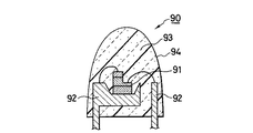
従来のこの種のLEDランプ90の構成の例を示すものが図5であり、このLEDランプ90のLEDチップ91としては、比較的に短波長の光を放射する窒化ガリウム系あるいはシリコンカーバイト系など化合物半導体のLEDチップ91を採用し、このLEDチップ91をリードフレーム92に導電性接着剤などによりダイボンドし配線を行った後に、蛍光体93を混和したエポキシ樹脂などによりモールドを行いケース94を形成するものである。
【0003】
このように形成することで、LEDランプ90から放射される光は、前記LEDチップ91が有する発光色と、前記蛍光体93が励起されて発する発光色との混合色と成る。よって、前記LEDチップ91の発光色と、蛍光体93の発光色とを補色の関係としておけば、LEDランプ90から外部に放射される光の発光色を白色とすることができる。
【0004】
【発明が解決しようとする課題】
しかしながら、前記した従来のLEDランプ90においては、第一にはケース94に蛍光体93を混和する際にエポキシ樹脂との均一な混合が難しく、不均一な分散状態となり、ケース94の部位によりLEDチップ91からの光と蛍光体93からの光との混合割合が異なるものとなり、いわゆる色ムラが発生し、LEDランプ90の品質が損なわれる問題点を生じている。
【0005】
第二には、如何に上記したエポキシ樹脂と蛍光体93とを均一に混和したとしても、蛍光体93はエポキシ樹脂よりも比重が大きいので、エポキシ樹脂が硬化するまでの間に蛍光体93が沈降し、ケース94として完成した時点では、上記と同様に色ムラを生じるものとなっている。
【0006】
また、上記した蛍光体93の沈降を防止するために沈降防止剤をエポキシ樹脂に添加する方法も提案されているが、この添加を行った場合にはエポキシ樹脂の接着性が極度に低下するものとなり、リードフレーム92およびLEDチップ91から剥離して湿度の浸入を許し、LEDチップ91が早期に劣化し、LEDランプ90の信頼性が低下する問題点を生じるものとなる。
【0007】
第三には、上記従来の構成のLEDランプ90においては、蛍光体93がケース94の全体にほヾ均一な割合として混和されているので、ケース94は全面で発光するものとなり、しかも、蛍光体93が励起されて発光する光が拡散光であることから、一方向に光を集中することができず、よって、光量が不足気味となる問題点も生じ、これらの点の解決が課題とされるものとなっていた。
【0008】
【課題を解決するための手段】
本発明は前記した従来の課題を解決するための具体的な手段として、少なくとも1個のLEDチップと、このLEDチップを一方の焦点とするときに他の一方となる焦点を有する二葉双曲面反射面と、前記二葉双曲面反射面の焦点と焦点を略一致させ前記LEDチップ側に向けて開口する回転放物面反射面とから成り、前記二葉双曲面反射面と回転放物面反射面との少なくとも一方には蛍光体が塗布されていることを特徴とする反射型LEDランプを提供することで課題を解決するものである。
【0009】
【発明の実施の形態】
つぎに、本発明を図に示す実施形態に基づいて詳細に説明する。図1は本発明の第一実施形態であり、図中に符号1で示すものは本発明に係る反射型LEDランプであり、この反射型LEDランプ1においても、窒化ガリウム系など適宜な発光色(例えばX=0.13、Y=0.09)を有するLEDチップ2をリードフレーム3にダイボンドして光源とするものである点は従来例のものと同様である。
【0010】
また、前記LEDチップ2およびリードフレーム3の一部がエポキシ樹脂などによるケース4で覆われるものとされている点も従来例と同様であるが、ここで本発明においては、前記ケース4に二葉双曲面反射面5と回転放物面反射面6とが設けられるものとされている。
【0011】
図2は前記二葉双曲面反射面5の形成手順を示すものであり、先ず、LEDチップ2から適宜の距離を有する点F2を設定し、前記LEDチップ2と点F2を焦点とする双曲線HP1、HP2を想定する。そして、前記LEDチップ2と点F2とを通る線を軸Xとして前記双曲線HP1、HP2に回転を行わせれば二葉双曲面が得られる。
【0012】
本発明では上記で得られる一対の二葉双曲面の内の、LEDチップ2を一方の焦点とするときに他の一方となる点F2を焦点とする二葉双曲面反射面5を採用するものである。また加えて、前記回転放物面反射面6について説明を行えば、この回転放物面反射面6は前記点F2を焦点とする放物線PBを前記軸Xで回転させて得られるものである。
【0013】
尚、実際の反射型LEDランプ1の製作に当たっては、ケース4は以後に説明する蛍光体7の配設などを可能とするために上記二葉双曲面反射面5と回転放物面反射面6とを境界としてケース上部41とケース下部42とに分割して形成されている。
【0014】
この第一形態においては、前記二葉双曲面反射面5に蛍光体7を設けるものであり、このときに、前記二葉双曲面反射面5と回転放物面反射面6とがケース上部41に設けられているのであれば、凹面となっている二葉双曲面反射面5の部分に印刷などで蛍光体7を膜面状に敷設する。このときに、この実施形態においては蛍光体7として、例えば励起される光が色度(X=0.497 、Y=0.496 )を有するYAG蛍光体などが採用されている。
【0015】
尚、このとき同時に前記回転放物面反射面6にはアルミニウムの真空蒸着などにより鏡面6aを形成しておく、また、この場合には前記ケース上部41には光の放射方向を二葉双曲面反射面5側に向けたLEDチップ2がリードフレーム3と共にモールドされ、前記LEDチップ2の背面側には投射レンズ41aが設けられている。
【0016】
そして、上記蛍光体7と鏡面6aが形成された後には、この蛍光体7と鏡面6aとを覆いケース下部42が樹脂モールドなどにより形成されて反射型LEDランプ1は完成されるものとなる。また、ケース下部42側に二葉双曲面反射面5と回転放物面反射面6とが設けられている場合にも略同様な手順で反射型LEDランプ1は完成される。
【0017】
ついで、上記の構成とした本発明の反射型LEDランプの作用および効果について説明する。先ずLEDチップ2から放射される光はその正面方向にある二葉双曲面反射面5に大部分が達するものとなり、この二葉双曲面反射面5に塗布された蛍光体7により色度が変換される。
【0018】
このときに前記LEDチップ2は双曲線の2つの焦点の一方の位置に置かれ、二葉双曲面反射面5は他の一方である点F2を焦点とするものであるので、二葉双曲面反射面5から反射する光は点F2から放射されるのと同じ状況となるが、前記回転放物面反射面6が点F2を焦点としているので、二葉双曲面反射面5に反射した光の内の回転放物面反射面6に到達したものは略平行光線となり投射レンズ41aに向かうものとなる。
【0019】
ここで、前記LEDチップ2から放射される光の全てが色度を変換されるものとはならず、前記投射レンズ41aから外部に放射される際には、LEDチップ2直接の発光色の光と、蛍光体7の発光色の光とが混色されるものとなり、この混色の比率を二葉双曲面反射面5の面積の調整するなど、適宜とすることで、例えば色度(X=0.31、Y=0.33)の白色光が得られるものとなる。
【0020】
図3に示すものは、本発明の第二実施形態であり、前の第一実施形態では二葉双曲面反射面5の側に蛍光体7が塗布されていたが、この第二実施形態では前記回転放物面反射面6の側に施すものである。この場合、二葉双曲面反射面5はLEDチップ2からの光に色変換を行うことなく回転放物面反射面6および投射レンズ41aに向けて反射させるものとなる。
【0021】
従って、投射レンズ41aから外部に放射される光にはLEDチップ2からの直射光の成分が増えることが期待できるので、上記したように白色光を得ようとするときに直射光の成分が不足するときには、この第二実施形態を実施すれば良いものとなる。尚、上記以外の部分における作用、効果は前の第一実施形態と同じであるので、ここでの詳細な説明は省略する。
【0022】
図4に示すものは、本発明の第三実施形態であり、この第三実施形態では二葉双曲面反射面5と回転放物面反射面6の双方に蛍光体7を塗布する。このときには双方の反射面5、6の全面を覆い蛍光体7を塗布しても良いものであるが、この第三実施形態では、二葉双曲面反射面5と回転放物面反射面6との双方にドット状として塗布している。そして、蛍光体7が塗布されない部分は鏡面5a、6aとされている。
【0023】
よって、投射レンズ41aから外部に放射される光の経路としては、▲1▼二葉双曲面反射面5の鏡面5aで反射し回転放物面反射面6の鏡面6aで反射するもの。▲2▼二葉双曲面反射面5の鏡面5aで反射し回転放物面反射面6の蛍光体7で反射するもの。▲3▼二葉双曲面反射面5の蛍光体7で反射し回転放物面反射面6の鏡面6aで反射するもの。▲4▼二葉双曲面反射面5の蛍光体7で反射し回転放物面反射面6の蛍光体7で反射するもの。
【0024】
即ち、この第三実施形態によれば、▲1▼で示したほとんど拡散が行われない光から▲4▼で示したほヾ完全な拡散が行われた光まで得られるものとなるので、光の混合は前の第一実施形態、第二実施形態よりも一層に確実に行われるものとなる。また、この第三実施形態では二葉双曲面反射面5に塗布する蛍光体7のドットの大きさと、回転放物面反射面6に塗布する蛍光体7のドットの大きさとを変えるなどすれば、より微細な調整が行えるものとなる。
【0025】
ここで、第一実施形態〜第三実施形態の総括を行えば、何れの実施形態も本発明により二葉双曲面反射面5と回転放物面反射面6とが設けられているものであるので、LEDチップ2から放射される光は大部分が二葉双曲面反射面5に達し更に回転放物面反射面6に反射して投射レンズ41a方向へ向かうものとなり、即ち、本発明の反射型LEDランプ1は指向性を有する配光特性が得られるものとなる。
【0026】
尚、本発明の実際の実施に当たり、例えば蛍光体7はチタン酸バリウムの白色粉末が混和されたものとし反射効率を高めるなど、従来から蛍光体7を使用する際に行われていた手法を採用するのは自由であり、同様に従来からLEDランプのケースの形成時に行われているように、ケース4に拡散材を混和するなども自由である。
【0027】
【発明の効果】
以上に説明したように本発明により、少なくとも1個のLEDチップと、このLEDチップを一方の焦点とするときに他の一方となる焦点を有する二葉双曲面反射面と、前記二葉双曲面反射面の焦点と焦点を略一致させ前記LEDチップ側に向けて開口する回転放物面反射面とから成り、前記二葉双曲面反射面と回転放物面反射面との少なくとも一方には蛍光体が塗布されている反射型LEDランプとしたことで、ケースを構成する樹脂に蛍光体を混和することをなくし、攪拌不足あるいは未硬化樹脂内での沈降による混合の不均一が生じることをなくし、色ムラの発生を防止して、この種の蛍光体を併用するLEDランプの性能向上に極めて優れた効果を奏するものである。
【0028】
また、ケースを構成する樹脂に蛍光体を混和することをなくしたことで、ケース内での光の散乱がなくなり二葉双曲面反射面および回転放物面反射面で設定された反射方向に光が集中するものとなり、従来からのLEDランプの特性であった指向性を有する配光特性が確保できるものとして、互換性を保つ優れた効果も奏するものである。
【図面の簡単な説明】
【図1】本発明に係る反射型LEDランプの第一実施形態を示す断面図である。
【図2】同じく本発明に係る反射型LEDランプの反射面の形成手段を示す説明図である。
【図3】同じく本発明に係る反射型LEDランプの第二実施形態を示す断面図である。
【図4】同じく反射型LEDランプの第三実施形態を示す断面図である。
【図5】従来例を示す断面図である。
【符号の説明】
1……反射型LEDランプ
2……LEDチップ
3……リードフレーム
4……ケース
41……ケース上部
41a……投射レンズ
42……ケース下部
5……二葉双曲面反射面
5a……鏡面
6……回転放物面反射面
6a……鏡面
7……蛍光体
Claims (2)
- 少なくとも1個のLEDチップと、このLEDチップを一方の焦点とするときに他の一方となる焦点を有する二葉双曲面反射面と、前記二葉双曲面反射面の焦点と焦点を略一致させ前記LEDチップ側に向けて開口する回転放物面反射面とから成り、前記二葉双曲面反射面と回転放物面反射面との少なくとも一方には蛍光体が塗布されていることを特徴とする反射型LEDランプ。
- 前記蛍光体は前記二葉双曲面反射面と回転放物面反射面との双方にドット状として塗布されていることを特徴とする請求項1記載の反射型LEDランプ。
Priority Applications (1)
| Application Number | Priority Date | Filing Date | Title |
|---|---|---|---|
| JP18889298A JP3624699B2 (ja) | 1998-07-03 | 1998-07-03 | 反射型ledランプ |
Applications Claiming Priority (1)
| Application Number | Priority Date | Filing Date | Title |
|---|---|---|---|
| JP18889298A JP3624699B2 (ja) | 1998-07-03 | 1998-07-03 | 反射型ledランプ |
Publications (2)
| Publication Number | Publication Date |
|---|---|
| JP2000022220A JP2000022220A (ja) | 2000-01-21 |
| JP3624699B2 true JP3624699B2 (ja) | 2005-03-02 |
Family
ID=16231719
Family Applications (1)
| Application Number | Title | Priority Date | Filing Date |
|---|---|---|---|
| JP18889298A Expired - Fee Related JP3624699B2 (ja) | 1998-07-03 | 1998-07-03 | 反射型ledランプ |
Country Status (1)
| Country | Link |
|---|---|
| JP (1) | JP3624699B2 (ja) |
Families Citing this family (13)
| Publication number | Priority date | Publication date | Assignee | Title |
|---|---|---|---|---|
| TW497277B (en) * | 2000-03-10 | 2002-08-01 | Toshiba Corp | Semiconductor light emitting device and method for manufacturing the same |
| JP2002195858A (ja) * | 2000-12-27 | 2002-07-10 | Nippon Seiki Co Ltd | 表示装置 |
| DE10065381B4 (de) * | 2000-12-27 | 2010-08-26 | Osram Opto Semiconductors Gmbh | Strahlungsemittierendes Halbleiterbauelement mit Lumineszenzkonversionselement |
| JP4825379B2 (ja) * | 2001-09-19 | 2011-11-30 | スタンレー電気株式会社 | 発光装置 |
| JP4172196B2 (ja) * | 2002-04-05 | 2008-10-29 | 豊田合成株式会社 | 発光ダイオード |
| JP2004047748A (ja) | 2002-07-12 | 2004-02-12 | Stanley Electric Co Ltd | 発光ダイオード |
| TW200414572A (en) | 2002-11-07 | 2004-08-01 | Matsushita Electric Ind Co Ltd | LED lamp |
| WO2005015646A1 (ja) | 2003-08-07 | 2005-02-17 | Matsushita Electric Industrial Co., Ltd. | Led照明光源 |
| JP3892030B2 (ja) | 2004-02-26 | 2007-03-14 | 松下電器産業株式会社 | Led光源 |
| JP2006269448A (ja) * | 2005-03-22 | 2006-10-05 | Stanley Electric Co Ltd | Led |
| US7703945B2 (en) * | 2006-06-27 | 2010-04-27 | Cree, Inc. | Efficient emitting LED package and method for efficiently emitting light |
| JP5446861B2 (ja) | 2007-04-17 | 2014-03-19 | 株式会社ニコン | 照明装置、プロジェクタ、およびカメラ |
| JP4110198B2 (ja) * | 2007-07-27 | 2008-07-02 | 株式会社東芝 | 半導体発光装置 |
Family Cites Families (8)
| Publication number | Priority date | Publication date | Assignee | Title |
|---|---|---|---|---|
| JPS5188036A (ja) * | 1975-01-29 | 1976-08-02 | ||
| JPS62164010A (ja) * | 1986-01-16 | 1987-07-20 | Ricoh Co Ltd | 赤外線カメラ |
| JPH01114666A (ja) * | 1987-10-27 | 1989-05-08 | Tohoku Electric Power Co Inc | 太陽熱機関用集熱装置 |
| JP2830025B2 (ja) * | 1988-10-25 | 1998-12-02 | 岩崎電気株式会社 | 発光ダイオード |
| JPH04106043U (ja) * | 1991-02-25 | 1992-09-11 | 日本板硝子株式会社 | 自動車用ストツプランプ |
| JPH0559402U (ja) * | 1992-01-14 | 1993-08-06 | 矢崎総業株式会社 | 光源用のリフレクタ装置 |
| JPH06151975A (ja) * | 1992-04-20 | 1994-05-31 | Victor Co Of Japan Ltd | 発光装置 |
| JP2939087B2 (ja) * | 1993-04-07 | 1999-08-25 | シャープ株式会社 | 全方位視覚系 |
-
1998
- 1998-07-03 JP JP18889298A patent/JP3624699B2/ja not_active Expired - Fee Related
Also Published As
| Publication number | Publication date |
|---|---|
| JP2000022220A (ja) | 2000-01-21 |
Similar Documents
| Publication | Publication Date | Title |
|---|---|---|
| JP3624699B2 (ja) | 反射型ledランプ | |
| US11525556B2 (en) | Light emitting device | |
| US7279719B2 (en) | Light emitting diode | |
| JP5130402B2 (ja) | 光線放射装置 | |
| US7753573B2 (en) | Light source and vehicle lamp | |
| US6900587B2 (en) | Light-emitting diode | |
| US8921877B2 (en) | Semiconductor light-emitting device for producing wavelength-converted light and method for manufacturing the same | |
| JP3707688B2 (ja) | 発光装置およびその製造方法 | |
| US8482016B2 (en) | Semiconductor light-emitting device and manufacturing method | |
| US8461610B2 (en) | Semiconductor light emitting device having a reflective material with a side slant surface and method of manufacturing | |
| US6890234B2 (en) | LED cross-linkable phosphor coating | |
| US8455907B2 (en) | Semiconductor light emitting device having an optical plate including a meniscus control structure and method of manufacturing | |
| CN101048879B (zh) | 发射电磁辐射的半导体器件和器件壳体 | |
| US8258527B2 (en) | Lighting device and semiconductor light source device | |
| JP4955422B2 (ja) | 発光装置 | |
| EP1276157A2 (en) | Shielded reflective light-emitting device | |
| KR101249010B1 (ko) | 발광 다이오드 칩 | |
| JP2012054084A (ja) | 照明装置 | |
| EP2593975B1 (de) | Strahlungsemittierendes bauelement | |
| JP2003124521A (ja) | ケース付半導体発光装置 | |
| JP2830025B2 (ja) | 発光ダイオード | |
| EP3239595B1 (en) | Lighting apparatus | |
| KR20230015968A (ko) | 형광체횔, 조명계 및 프로젝터 | |
| JP7060819B2 (ja) | 発光装置 | |
| JP2023050923A (ja) | 発光装置及びその製造方法 |
Legal Events
| Date | Code | Title | Description |
|---|---|---|---|
| A977 | Report on retrieval |
Free format text: JAPANESE INTERMEDIATE CODE: A971007 Effective date: 20041026 |
|
| TRDD | Decision of grant or rejection written | ||
| A01 | Written decision to grant a patent or to grant a registration (utility model) |
Free format text: JAPANESE INTERMEDIATE CODE: A01 Effective date: 20041102 |
|
| A61 | First payment of annual fees (during grant procedure) |
Free format text: JAPANESE INTERMEDIATE CODE: A61 Effective date: 20041122 |
|
| R150 | Certificate of patent (=grant) or registration of utility model |
Free format text: JAPANESE INTERMEDIATE CODE: R150 |
|
| FPAY | Renewal fee payment (prs date is renewal date of database) |
Free format text: PAYMENT UNTIL: 20071210 Year of fee payment: 3 |
|
| FPAY | Renewal fee payment (prs date is renewal date of database) |
Free format text: PAYMENT UNTIL: 20091210 Year of fee payment: 5 |
|
| FPAY | Renewal fee payment (prs date is renewal date of database) |
Free format text: PAYMENT UNTIL: 20091210 Year of fee payment: 5 |
|
| FPAY | Renewal fee payment (prs date is renewal date of database) |
Free format text: PAYMENT UNTIL: 20101210 Year of fee payment: 6 |
|
| FPAY | Renewal fee payment (prs date is renewal date of database) |
Free format text: PAYMENT UNTIL: 20111210 Year of fee payment: 7 |
|
| FPAY | Renewal fee payment (prs date is renewal date of database) |
Free format text: PAYMENT UNTIL: 20111210 Year of fee payment: 7 |
|
| FPAY | Renewal fee payment (prs date is renewal date of database) |
Free format text: PAYMENT UNTIL: 20121210 Year of fee payment: 8 |
|
| FPAY | Renewal fee payment (prs date is renewal date of database) |
Free format text: PAYMENT UNTIL: 20121210 Year of fee payment: 8 |
|
| FPAY | Renewal fee payment (prs date is renewal date of database) |
Free format text: PAYMENT UNTIL: 20131210 Year of fee payment: 9 |
|
| LAPS | Cancellation because of no payment of annual fees |