EP1065720A2 - Treiber-IC-Modulgehäuse und Flachbildschirm damit - Google Patents
Treiber-IC-Modulgehäuse und Flachbildschirm damit Download PDFInfo
- Publication number
- EP1065720A2 EP1065720A2 EP00303447A EP00303447A EP1065720A2 EP 1065720 A2 EP1065720 A2 EP 1065720A2 EP 00303447 A EP00303447 A EP 00303447A EP 00303447 A EP00303447 A EP 00303447A EP 1065720 A2 EP1065720 A2 EP 1065720A2
- Authority
- EP
- European Patent Office
- Prior art keywords
- driver
- wirings
- substrate
- earth
- chip
- Prior art date
- Legal status (The legal status is an assumption and is not a legal conclusion. Google has not performed a legal analysis and makes no representation as to the accuracy of the status listed.)
- Withdrawn
Links
Images


Classifications
-
- G—PHYSICS
- G09—EDUCATION; CRYPTOGRAPHY; DISPLAY; ADVERTISING; SEALS
- G09G—ARRANGEMENTS OR CIRCUITS FOR CONTROL OF INDICATING DEVICES USING STATIC MEANS TO PRESENT VARIABLE INFORMATION
- G09G3/00—Control arrangements or circuits, of interest only in connection with visual indicators other than cathode-ray tubes
- G09G3/04—Control arrangements or circuits, of interest only in connection with visual indicators other than cathode-ray tubes for presentation of a single character by selection from a plurality of characters, or by composing the character by combination of individual elements, e.g. segments using a combination of such display devices for composing words, rows or the like, in a frame with fixed character positions
- G09G3/06—Control arrangements or circuits, of interest only in connection with visual indicators other than cathode-ray tubes for presentation of a single character by selection from a plurality of characters, or by composing the character by combination of individual elements, e.g. segments using a combination of such display devices for composing words, rows or the like, in a frame with fixed character positions using controlled light sources
- G09G3/10—Control arrangements or circuits, of interest only in connection with visual indicators other than cathode-ray tubes for presentation of a single character by selection from a plurality of characters, or by composing the character by combination of individual elements, e.g. segments using a combination of such display devices for composing words, rows or the like, in a frame with fixed character positions using controlled light sources using gas tubes
-
- G—PHYSICS
- G02—OPTICS
- G02F—OPTICAL DEVICES OR ARRANGEMENTS FOR THE CONTROL OF LIGHT BY MODIFICATION OF THE OPTICAL PROPERTIES OF THE MEDIA OF THE ELEMENTS INVOLVED THEREIN; NON-LINEAR OPTICS; FREQUENCY-CHANGING OF LIGHT; OPTICAL LOGIC ELEMENTS; OPTICAL ANALOGUE/DIGITAL CONVERTERS
- G02F1/00—Devices or arrangements for the control of the intensity, colour, phase, polarisation or direction of light arriving from an independent light source, e.g. switching, gating or modulating; Non-linear optics
- G02F1/01—Devices or arrangements for the control of the intensity, colour, phase, polarisation or direction of light arriving from an independent light source, e.g. switching, gating or modulating; Non-linear optics for the control of the intensity, phase, polarisation or colour
- G02F1/13—Devices or arrangements for the control of the intensity, colour, phase, polarisation or direction of light arriving from an independent light source, e.g. switching, gating or modulating; Non-linear optics for the control of the intensity, phase, polarisation or colour based on liquid crystals, e.g. single liquid crystal display cells
- G02F1/133—Constructional arrangements; Operation of liquid crystal cells; Circuit arrangements
- G02F1/1333—Constructional arrangements; Manufacturing methods
- G02F1/1345—Conductors connecting electrodes to cell terminals
- G02F1/13452—Conductors connecting driver circuitry and terminals of panels
-
- H—ELECTRICITY
- H01—ELECTRIC ELEMENTS
- H01J—ELECTRIC DISCHARGE TUBES OR DISCHARGE LAMPS
- H01J11/00—Gas-filled discharge tubes with alternating current induction of the discharge, e.g. alternating current plasma display panels [AC-PDP]; Gas-filled discharge tubes without any main electrode inside the vessel; Gas-filled discharge tubes with at least one main electrode outside the vessel
- H01J11/20—Constructional details
- H01J11/46—Connecting or feeding means, e.g. leading-in conductors
-
- H—ELECTRICITY
- H05—ELECTRIC TECHNIQUES NOT OTHERWISE PROVIDED FOR
- H05K—PRINTED CIRCUITS; CASINGS OR CONSTRUCTIONAL DETAILS OF ELECTRIC APPARATUS; MANUFACTURE OF ASSEMBLAGES OF ELECTRICAL COMPONENTS
- H05K7/00—Constructional details common to different types of electric apparatus
- H05K7/20—Modifications to facilitate cooling, ventilating, or heating
- H05K7/20954—Modifications to facilitate cooling, ventilating, or heating for display panels
- H05K7/20963—Heat transfer by conduction from internal heat source to heat radiating structure
-
- H—ELECTRICITY
- H01—ELECTRIC ELEMENTS
- H01J—ELECTRIC DISCHARGE TUBES OR DISCHARGE LAMPS
- H01J2217/00—Gas-filled discharge tubes
- H01J2217/38—Cold-cathode tubes
- H01J2217/49—Display panels, e.g. not making use of alternating current
- H01J2217/492—Details
-
- H—ELECTRICITY
- H05—ELECTRIC TECHNIQUES NOT OTHERWISE PROVIDED FOR
- H05K—PRINTED CIRCUITS; CASINGS OR CONSTRUCTIONAL DETAILS OF ELECTRIC APPARATUS; MANUFACTURE OF ASSEMBLAGES OF ELECTRICAL COMPONENTS
- H05K1/00—Printed circuits
- H05K1/02—Details
- H05K1/0201—Thermal arrangements, e.g. for cooling, heating or preventing overheating
- H05K1/0203—Cooling of mounted components
- H05K1/0204—Cooling of mounted components using means for thermal conduction connection in the thickness direction of the substrate
- H05K1/0206—Cooling of mounted components using means for thermal conduction connection in the thickness direction of the substrate by printed thermal vias
-
- H—ELECTRICITY
- H05—ELECTRIC TECHNIQUES NOT OTHERWISE PROVIDED FOR
- H05K—PRINTED CIRCUITS; CASINGS OR CONSTRUCTIONAL DETAILS OF ELECTRIC APPARATUS; MANUFACTURE OF ASSEMBLAGES OF ELECTRICAL COMPONENTS
- H05K1/00—Printed circuits
- H05K1/02—Details
- H05K1/14—Structural association of two or more printed circuits
- H05K1/147—Structural association of two or more printed circuits at least one of the printed circuits being bent or folded, e.g. by using a flexible printed circuit
-
- H—ELECTRICITY
- H05—ELECTRIC TECHNIQUES NOT OTHERWISE PROVIDED FOR
- H05K—PRINTED CIRCUITS; CASINGS OR CONSTRUCTIONAL DETAILS OF ELECTRIC APPARATUS; MANUFACTURE OF ASSEMBLAGES OF ELECTRICAL COMPONENTS
- H05K1/00—Printed circuits
- H05K1/18—Printed circuits structurally associated with non-printed electric components
- H05K1/182—Printed circuits structurally associated with non-printed electric components associated with components mounted in the printed circuit board, e.g. insert mounted components [IMC]
-
- H10W90/754—
Definitions
- the present invention relates to a driver IC packaging module and a flat display device using the same.
- FIG. 1 is a schematic plan view showing an example of an AC PDP device with a triple-electrode surface discharge structure and a block diagram showing a driver circuit therein.
- FIG.2 is a sectional view showing display cells in the AC PDP device.
- a front glass substrate 101 and a rear glass substrate 102 are arranged at a distance to oppose to each other.
- a plurality of display sustaining electrodes made of transparent conductive material are formed in parallel on an opposing surface of the front glass substrate 101 opposing to the rear glass substrate 102.
- the sustaining electrodes consist of X electrodes x n (n is an integer) and Y electrodes y n (n is an integer), which are arranged alternatively.
- the sustaining voltage is applied to the X electrode x n and the Y electrode y n which partition one luminous displayed cell area 103.
- a plurality of address electrodes a m are arranged on an opposing surface of the rear glass substrate 102 opposing to the front glass substrate 101 so as to intersect orthogonally with the sustaining electrodes x n , y n .
- the space where one address electrode am intersects with a pair of sustaining electrodes x n , y n constitutes a single display cell 103.
- either display or non-display of the display cell 103 can be selected.
- the sustaining electrodes x n , y n are covered with a protection film 104, and the address electrodes a m is covered with a dielectric film 105.
- Insulating partitions 106 are formed on respective areas of the dielectric film 105 on both sides of the address electrodes a m .
- Red, green, or blue fluorescent material 107 is coated on a surface of the dielectric film 105 between the partitions 106.
- an inter-opposing electrode capacitance Cg is present between the address electrode am and the sustaining electrodes x n , y n , and an inter-neighboring electrode capacitance Ca is present between the address electrodes a m .
- principal portions of the AC PDP driver circuit comprises an address driver circuit 111 for driving the address electrodes a m , a scanning driver circuit 112 for driving and scanning the Y electrodes y n Independently, a Y common driver circuit 113 for applying the sustaining voltage to the Y electrodes y n via the scanning driver circuit 112, an X common driver circuit 114 for applying the sustaining voltage to the X electrodes x n and, a controller circuit 115 for controlling these driver circuits 111 to 114.
- the controller circuit 115 comprises a display data controller 116 for driving the address driver circuit 111 based on a clock signal CLK and display data D supplied from external devices, a scanning driver controller 117 for driving the scanning driver circuit 112 in accordance with the horizontal synchronizing signal H sync and the vertical synchronizing signal V sync supplied from external devices and, a common driver controller 118 for driving the X common driver circuit 114 and the Y common driver circuit 113 in accordance with the horizontal synchronizing Signal H sync and the vertical synchronizing signal V sync being input from external devices.
- the display data controller 116 has a frame memory 119 for storing display data.
- the scanning driver circuit 112 and the address driver circuit 111 need circuits which apply selectively a driving pulse to a plurality of Y electrodes y n and a plurality of address electrodes a m .
- IC semiconductor devices are employed as principal circuit parts in such circuits.
- the drivers which have output pads connected to these electrodes on a one-by-one correspondence are required.
- driver IC chip in which 64 driver elements for driving 64 electrodes are integrated is employed as such drivers.
- driver ICs are prepared for the 480 Y electrodes on the Y electrode side, and 40 driver ICs are prepared for the 2556 address electrodes on the address electrode side.
- driver circuits In order to incorporate a number of driver ICs into the PDP device as the driver circuits, high density packaging technology is required which can provide electrical connection to a number of electrodes without fail with high reliability, and which can mount these small and thin driver circuits on the rear side of the display panel.
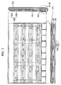
- a previously-considered PDP device has such a structure that a display panel 123 is stuck on one surface of a chassis 122 which is constructed by intersecting a plurality of beam members 120, 121 mutually.
- a plurality of driver IC chips are mounted on the other surface of the chassis 122.
- Each of the beam members 120, 121 is formed as a metal rod body which has a sectional shape like a hat.
- driver IC chip packaging structure As the driver IC chip packaging structure, one approach is to integrate a plurality of driver IC chips on one substrate as a module and then to incorporate this module into the PDP device.
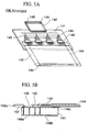
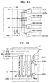
- Example structures for the driver IC packaging module include the COB (Chip On Board) structure shown in FIGS.4A and 4B and the COM (Chip On Multiple Board) structure shown in FIGS.5A and 5B.
- the COB structure comprises a printed substrate 131, a flexible flat cable (abbreviated simply as "FFC” hereinafter) 132 which is thermocompression-bonded to one side portion of the printed substrate 131, and a flexible substrate 133 which is thermocompression-bonded to the other side portion of the printed substrate 131.
- the COB structure has such a structure that a plurality of bare-chip driver ICs 130 are directly mounted on the printed substrate 131 and various pads (not shown) on the driver ICs 130 are connected to wirings 134, 135 on the printed substrate 131 via the wire bonding.
- the pads on the driver ICs 130 there are power supply pads, input signal pads, output pads, etc.
- a plurality of wirings 135 on the output side on the printed substrate 131 are connected to a plurality of wirings 136 on the flexible substrate 133 one by one by the thermocompression bonding respectively. Also, a plurality of wirings 134 on the input side on the printed substrate 131 are connected to a plurality of wirings 137 on the FFC 132 one by one by the solder respectively.
- a reference 138a denotes input signal and power supply wiring patterns formed on a back surface of the printed substrate 131 on the input side.
- the wiring patterns 138a have a three-dimensional wiring structure which can distribute various wirings being input from the FFC 132 to a plurality of driver ICs 130 by utilizing through-holes or wiring patterns on the back surface of the substrate.
- a reference 138b denotes a high voltage power supply pattern formed on the back surface on the output side
- 138c denotes an earth pattern formed below the driver ICs 130 on the back surface
- 139 denotes a voltage power supply pattern formed on an upper surface of the printed substrate 131.
- the COM structure comprises a printed substrate 141, an FFC 142 which is adhered to one side portion of the printed substrate 141 by the solder, and a flexible substrate 143 which is adhered to the other side portion of the printed substrate 141.
- a plurality of pads on the bare chip driver ICs 140 on the output side are connected to a plurality of wirings 146 on the flexible substrate 143 one by one via the wire bonding.
- the input signal and power supply wiring patterns 145 on the printed substrate 141 have a three-dimensional wiring structure which can distribute various wirings being input from the FFC 142 to a plurality of driver ICs 140 by utilizing through-holes in the substrate or wiring patterns on the back surface of the substrate.
- One ends of these wirings 145 are connected one by one to input signal and power supply pads of respective driver ICs 140 by the wire bonding.
- a reference 148a denotes input signal an power supply wiring patterns formed on the back surface of the printed substrate 141 on the input side
- 148b denotes an earth pattern formed on the back surface below the driver ICs 140
- 148c denotes high voltage power supply patterns formed on the output side of the surface of the printed substrate 141.
- the COM structure can achieve higher reliability and higher density than the COB structure.
- the output sides of the wirings on the flexible substrates 134, 144 are exposed in the opposite direction to the upper surfaces of the printed substrates 131, 141 (fitting surfaces of the driver ICs 130, 140) in the COB structure and the COM structure.
- the mounting surface of the driver ICs 130 and the exposed surface of output ends of the wirings 136 on the flexible substrate are directed in the opposite direction to each other in the COB structure, whereas the mounting surface of the driver ICs 140 and the exposed surface of output ends of the wirings 146 on the flexible substrate 143 are directed in the same direction in the COM structure.
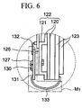
- the driver IC packaging module M1 having the COB structure shown in FIGS.4A and 4B are secured onto the beam elements 121 of the chassis 122 by driving screws 127 via an insulating sheet 126 and the printed substrate 131 into the beam elements 121, as shown in FIG.6, for example.
- the module M1 can be fitted to be secured such that the back side of the IC chip mounting surface is directed to the panel 123.
- the printed substrate 131 may be fixed to the chassis 122 by the screws using cylindrical bosses in place of the insulating sheet 126.
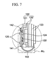
- the driver IC packaging module M2 having the COM structure shown in FIG.5 can be fitted to secure the printed substrate 141 to top surfaces of the cylindrical bosses 124, which are fitted onto the beam member 121 of the chassis 122, as shown in FIG.7, for example, by using screws 125.
- the IC chip mounting surface of the printed substrate 141 and the exposed surfaces of the wirings 146 on the flexible substrate 143 are directed to the same direction, the IC chip mounting surface of the printed substrate 141 can be secured to direct to the panel 123.
- the driver IC packaging module has a plurality of driver ICs 130, 140 described above, and a high voltage power supply line V H , a low voltage power supply line V L , a signal line SG, and a ground voltage line GND are connected to respective input pads of the driver ICs 130, 140.
- a high voltage bypass capacitor C H is connected between the high voltage power supply line V H and the ground voltage line GND, and a low voltage bypass capacitor C H is connected between the low voltage power supply line V L and the ground voltage line GND.
- the high voltage power supply line V H , the low voltage power supply line V L , the signal line SG, and the ground voltage line GND are input from wirings of the flexible flat cable (FFC), then divided into plural lines via input wirings on the substrate side, and then input into the driver ICs 130, 140 in parallel.
- the signal line SG has a plurality of wirings to transmit a clock signal CLK, data D, a latch signal LATCH, and a strobe signal STB.
- the driver ICs 130, 140 have such a structure that a 64-bit shift register SR, a 64-bit latch L, and a 64-bit gate G are connected in series.
- a data signal D and a clock signal CLK are input into the 64-bit shift register SR via a signal line, and also a low voltage is applied to the 64-bit shift register SR from the low voltage power supply line V L .
- the latch signal LACH is input into the 64-bit latch L
- the strobe signal STB is input into the 64-bit gate G.
- the ground voltage line GND is connected to the 64-bit shift register SR, the 64-bit latch L, and the 64-bit gate G respectively.
- output buffers BF 1 to BF 64 are connected to 64 output terminals of the 64-bit gate G individually.
- the high voltage power supply line V H and the ground voltage line GND are connected to power supply ends of these connection buffers BF 1 to BF 64 to supply a high voltage.
- a low voltage signal is input into signal input ends of the connection buffers BF 1 to BF 64 such that a high voltage signal is output from their output ends in response to the signal.
- the signal output from the output ends is sent to the address electrodes a m .
- the emissive display panel such as the AC PDP device, the EL display device, etc.
- the supply of the luminescence energy to pixels is needed based on the principle operation characteristic. Therefore, there is such a tendency that the current flowing through the inside of the driver IC is increased to enhance an amount of heat generation in the driver IC itself and thus power loss in the inside is increased up to an unnegligible level.
- the heat generated in the driver IC 130 has no means of escape except through the printed substrate 131 and thus such heat is kept between the printed substrate 131 and the frame 122. Therefore, there is a possibility that, since the temperature of the driver IC 130 itself is increased, the long-term reliability cannot be assured.
- the driver IC packaging module having the COB structure shown in FIGS. 4A, 4B and 6 and the fitting structure described above, a part of the chassis 122 is utilized as a radiation board. It is preferable that the heat should be radiated from the driver IC 130 by providing a convex tool to the chassis 122 or bringing the back surface of the printed substrate 131 into contact with the chassis 122 directly.
- the driver IC packaging module having the COB structure described above since the high voltage power supply wiring and the signal line are formed on the back surface side of the printed substrate 131, it is impossible to bring the back surface of the printed substrate 131 into contact to the tool or the chassis directly and thus the insulating sheet 126 cannot be omitted.
- the heat radiation from the printed substrate 131 to the chassis 122 is carried out via the insulating sheet 126. Therefore, it is the existing state that the heat radiation effect has the limit and does not come up to a level which can assure the reliability.
- the configuration for connecting the output side wirings on the printed substrate 131 and the wirings on the flexible substrate 133 mutually by the thermocompression bonding is indispensable for the COB structure.
- pitches of the wirings which are arranged in great numbers on the printed substrate 131 and the flexible substrate 133 are fine, short-circuits can occur between the wirings when alignment of the opposing wirings is displaced. Defective contact due to mixture of foreign matters also occurs easily.
- the definition of the wiring pitch increases and the wiring length becomes longer, it becomes more difficult to assure connection quality and reliability.
- driver IC packaging module which includes an IC module having a high heat radiating effect or a chassis structure having a high heat radiating efficiency, and a flat display device using the same.
- one end portion, which are connected to the display panel electrodes, of the wirings which are passed through the flexible substrate fitted to an area located in the neighborhood of one end of the driver IC chip mounting surface is exposed in the opposite direction to the driver IC chip mounting surface.
- the driver IC chip mounting surface it is possible to direct the driver IC chip mounting surface to the rear surface side and connect one end portion of the electrodes of the flexible substrate to electrodes on a front surface of the display panel by bending the flexible substrate.
- a structure which brings the back surface (surface opposite to the driver IC chip mounting surface) of the module substrate into contact with the surface of the chassis can be achieved easily, the chassis per se can be ready to be utilized as the heat radiation plate for the heat generated by the substrate, and thus a structure of the flat display device which can improve the thermal characteristic of the module and can be installed compactly can be achieved.
- the mechanical strength can be maintained by attaching a beam-like structure to the chassis on the rear surface of the display panel or forming a part of the chassis itself as the beam-like structure, and also the substrate surface of the driver IC packaging module can come into contact into the flat plate surface of this beam-like structure. Therefore, the heat generated from the driver IC chip can be diffused to the chassis via the beam.
- the thermal characteristic can be improved by causing the chassis per se to have the function of radiating the heat generated by the driver IC chip, and also the built-in packaging structure whose thickness is small and whose thermal characteristic can be improved as a whole can be achieved while holding the original mechanical strength of the chassis as it is.
- the chassis is formed of the flat metal plate having a size to cover substantially the overall rear surface side of the panel, because the chassis is formed to have a wide area, such chassis can have the effect as the heat radiation and thermal diffusion plate for not only the heat generated by the driver IC chip but also the heat generated by the display panel and other driver circuit substrates. Therefore, the thermal characteristic of the overall device can be improved and the mechanical strength can be still maintained by attaching the beam. As a result, a thin flat display device having sufficient mechanical strength can be achieved.
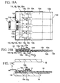
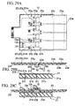
- FIG.9A is a plan view showing a first driver IC packaging module according to a first embodiment of the present invention
- FIG.9B is a sectional view showing the same
- FIG.10A is a plan view showing a second driver IC packaging module according to the first embodiment of the present invention
- FIG.9B is a sectional view showing the same.
- the driver IC packaging module described in the following explanation will be made under the assumption that the side of the module connected to the display panel is the output side and the side connected to the device on the chassis is the input side. But these terms of the "input side" of the "output side” should not be interpreted to restrict the propagation direction of the actual signal.
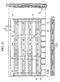
- a plurality of die bonding patterns (earth patterns) 11h on which driver IC chips 10 are mounted are formed in a central area of an upper surface of the printed substrate 11 which is formed of insulating material such as glass epoxy, bakelite, etc.
- a plurality of input terminals 11c connected to external circuits, and control input signal wirings 11d, low voltage power supply wirings 11e, high voltage power supply wirings 11f, and earth wirings 11g all being connected to the input terminals 11c are formed in an input side area of an upper surface of the printed substrate 11.
- the input signal wirings 11d are formed at a pitch of several hundreds ⁇ m and the low voltage power supply wirings 11e are formed.
- a high voltage power supply plane 11i which is connected to the high voltage power supply wirings 11f and is formed solidly.
- the back surface of the driver IC chip 10 is secured to the die bonding pattern 11h, which is set to an earth potential, by conductive adhesive.
- Pads 10a on the driver IC chip 10 are wire-bonded to the die bonding pattern 11h, the input signal wirings 11d, the low voltage power supply wirings 11e, the high voltage power supply plane 11i, etc. via conductive lines 10b.
- the die bonding pattern 11h, the input signal wirings 11d, the low voltage power supply wirings 11e, the high voltage power supply plane 11i, etc. are formed by patterning a copper foil of about 18 to 35 ⁇ m thickness respectively by virtue of the photolithography.
- Cross wirings which distribute the input signal wirings lid and the low voltage power supply wirings 11e, which are input from the input terminals 11c, to four driver IC chips 10 are formed in the input area of the printed substrate 11.
- the cross wirings are formed to intersect a plurality of through holes 11n, 11p and a plurality of wirings 11j, 11k formed on the lower surface and re-arrange them in the neighborhood of the input side of the driver IC chips 10 on the upper surface.
- An earth plane 11m is formed solidly in a wide area from a center of the lower surface of the printed substrate 11 to the output side. This earth plane 11m is connected electrically to the die bonding pattern 11h via through holes 11g which also functions as a thermal via.
- a flexible substrate 12 having a plurality of copper wirings 12c which are put between base films 12a and covering films 12b formed of insulating material such as polyester, polyimide, etc. is fitted.
- Output end areas 12e of the copper wirings 12c are exposed downward and input end areas 12d are exposed upward. That is, exposed surfaces of the output end areas 12e and exposed surfaces of the input end areas 12d of the wirings 12c on the flexible substrate 12 are directed oppositely mutually.
- the input end areas 12d of the wirings 12c on the flexible substrate 12 and the bonding pads 10a of the driver IC chips 10 are connected mutually via the conductive lines 10b by virtue of the wire bonding method.
- Chip capacitors 13a, 13b which act as bypass capacitors between the low voltage power supply wirings 11e, the high voltage power supply wirings 11f and the earth wirings 11g respectively are surface-mounted on the above input side area of the upper surface of the printed substrate 11.
- the FFC 14 has an insulating covering film 14a formed of polyester, polyimide, etc. to cover the conductive lines 14b.
- Fixing holes 11b are opened in the input side areas of the printed substrate 11 near both ends respectively.
- the printed substrate 11 can be fixed to the chassis of the display device by passing screws etc. through these fixing holes 11b.
- the driver IC packaging module shown in FIG.9 shows an example in which the FFC 14 is employed in the input portion
- the connector may be employed.
- the case where the connectors 15 are mounted on the lower surface side of the input portion of the printed substrate 11 is shown in FIG.10. That is, the connectors 15 are soldered to the through holes and the land portions on the upper surface side of the input area of the printed substrate 11 to project the pins 15a. Remaining configurations are similar to those in FIG.9 and their redundant explanation will be omitted in this disclosure.
- the above driver IC packaging modules shown in FIGS.9 and 10 are incorporated into the flat display device such as the PDP device shown in FIG.11, for example.
- the PDP device shown in FIG.11 has such a structure that the back surface of the display panel 5 is stuck onto a surface of the chassis 4 which is constructed by intersecting a plurality of first beam members 2 and a plurality of second beam members 3 mutually and a plurality of driver IC packaging modules M are mounted onto the other surface of the chassis 4.
- Each of the first beam members 2 and the second beam members 3 is formed of a metal rod body which has a hat-like sectional shape. Their intersecting portions are fixed by the caulking using TOX, HENROBRIVETS, etc.
- the display panel 5 consists of the front and rear glass substrates 101, 102 on which electrodes, fluorescent material, etc. shown in FIGS.1 and 2 are formed.
- An address driver arrange area A1, a scanning driver arrange area A2, an X common driver arrange area A3, a Y common driver arrange area A4, a control circuit substrate arrange area A5, a power supply arrange area A6, an X side distribution wiring substrate arrange area A7, and an address bus substrate arrange area A8 are prepared on the other surface of the chassis 4.
- the driver IC packaging module M is fitted in the address driver arrange area A1 on the chassis 4.
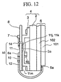
- FIG.12 is an enlarged view of a portion indicated by a broken line shown in FIG.11.
- the printed substrate 11 of the driver IC packaging module M is secured onto the chassis 4 by screws 6a such that the lower earth plane 11m comes into contact to the second beam member 3. That is, press nuts 6b are press-fitted from the back side of the beam member 3, then the press nuts 6b and fitting holes 11b of the printed substrate 11 are superposed, and then the printed substrate 11 is fixed onto the beam member 3 by the screws 6a. Accordingly, the earth plane 11m is held at an earth potential via not only the earth wirings from the FFC 14 but also the second beam member 3.
- concave portions 3a are formed in areas of the second beam member 3, in which the low voltage power supply wirings 11k and the input signal wirings 11j on the lower surface side of the printed substrate 11 are positioned. Accordingly, as indicated by a chain double-dashed line shown in FIG.9B, the low voltage power supply wirings 11k and the input signal wirings 11j are positioned not to come into contact to the second beam member 3.
- the flexible substrate 12 is curved to the display panel 5 side, and then the output ends 12e of the wirings 12c of the flexible substrate 12 are connected electrically to front electrodes 5a of the rear glass substrate 102 by the thermocompression bonding.
- the input ends 14c of the wirings 14b of the FCC 14 are connected to the bus substrates 8 or control circuit substrates (not shown) on the panel 4 via the connectors 7.
- These bus substrates 8 are fitted onto the beam member 3 in the address bus substrate arrange area A8, and the control circuit substrates are fitted onto the beam member 3 in the control circuit substrate arrange area A5.
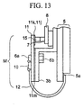
- FIG.13 shows the state that the driver IC packaging module is fitted onto the uppermost surface of the beam member 3b having a Z-type sectional shape and then the connectors 15 of the driver IC packaging module are connected to the connectors 7 of the bus substrates 8.
- the printed substrate 11 is secured onto the uppermost surface of the beam member 3b by using the screws 6a and the press nuts 6b under the condition that the earth planes 11m are connected to the beam member 3b.
- the low voltage power supply wirings 11k and the input signal wirings 11j on the lower surface (back surface) side of the printed substrate 11 are positioned over the bus substrates 8 or the control circuit substrates (not shown) via the connectors 7, 15.
- the driver IC packaging module which is fitted onto the chassis 4 in the above state can radiate effectively the heat of the driver IC chip 10 to the outside since the printed substrate 11 comes into contact to the chassis 4 via the copper earth planes 11m.
- the chassis 4 is used as a heat sink.
- the concave portions 3a are formed in the portions of the beam member 3 of the chassis 4, which oppose to the low voltage power supply wirings 11k and the input signal wirings 11j, short-circuit between the wirings can be avoided.
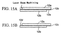
- a method of using the laser beam machining, as shown in FIGS.14A to 14D, will be explained as the first method of forming the flexible substrate 12.
- the copper foil is pasted on the base film 12a which is formed of insulating resin such as polyimide, polyester, etc., and then a plurality of wirings 12c are formed in parallel by patterning the copper foil by means of the photolithography method.
- a covering film 12b formed of insulating resin is stuck onto the wirings 12c by the thermocompression bonding.
- one end of the base film 12a is displaced with one end of the covering film 12b to expose the input side area 12d of the wiring 12c, to which the wire bonding can be applied.
- the base film 12a is removed partially by irradiating the excimer laser to the other end of the base film 12a and its neighboring area to expose the output end area 12e of the wiring 12c.
- the input end area 12d and the output end area 12e of the wiring 12c are exposed in the opposite direction respectively. Accordingly, the flexible substrate 12 can be completed.
- the input end area 12d of the wiring 12c is exposed to paste the covering film 12b onto the base film 12a.
- the arrangement of the base film 12a and the covering film 12b may be reversed, and then the output end area 12e of the wiring 12c may be exposed to paste the covering film 12b onto the base film 12a.
- the input end area 12d of the base film 12a is removed partially by the laser irradiation.
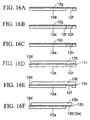
- a method of using the prepunch method, as shown in FIGS.16A to 16F, will be explained as the second method of forming the flexible substrate 12.
- a window 12f is formed in an area near one end of the base film 12a, and then the copper foil 12g is pasted on the base film 12a.
- an implementing agent 12h formed of predetermined agent used for the copper foil etching is coated in the window 12f.
- a plurality of wirings 12c are formed by patterning the copper foil 12g by virtue of the photolithography method.
- the covering film 12b formed of insulating resin is pasted onto the base film 12a by the thermocompression bonding.
- the other end of the base film 12a is displaced with the other end of the covering film 12b to expose the other end of the wiring 12c and its peripheral area in the opposite direction to the window 12f.
- the implementing agent 12h is removed.
- respective layers from the base film 12a to the covering film 12b located in an area which extends from the window 12f to one end are cut out to remove, whereby the steps of forming the flexible substrate 12 are completed.
- the wirings 12c of the flexible substrate 12 and the pads 10a of the driver IC chip 10 are connected via the conductive line 10b, but the present invention is not limited to such connection.
- such a configuration may be adopted that input end areas 16d of wirings 16c of the flexible substrate 16 are directly bonded to the pads 10a of the driver IC chip 10 by using bumps, an anisotropic conductive film, or a conductive adhesive.
- the positional relationship between the base film 16a and the covering film 16b of the flexible substrate 16 is reversed in contrast to the first embodiment so as to bring the covering film 16b into contact to the printed substrate 11, and then the input end area 16d and the output end area 16e of the wiring 16c are not exposed from the base film 16a, but exposed from both end portions of the covering film 16b in the same direction. Accordingly, since the input end area 16d of the wiring 16c of the flexible substrate 16 and the pads 10a of the driver IC chip 10 can be collectively connected by the bonding, the time required for connection can be reduced and thus a lower cost can be achieved.
- the pads 10a of the driver IC chip 10 and the input end area 16d of the wiring 16c of the flexible substrate 16 are bonded collectively.
- the driver IC chips 10 are die-bonded onto the die bonding patterns 11h of the printed substrate 11, and also the flexible substrate 16 is pasted onto the surface of the printed substrate 11 by the adhesive.
- the input signal wirings 11d, the low voltage power supply wirings 11e, the die bonding patterns 11h, and the high voltage power supply wirings 11i on the printed substrate 11 are connected to the corresponding pad terminals 10a of the driver IC chips 10 via the conductive lines 10b respectively by the wire bonding, whereby electrical connection can be completed.
- driver IC packaging module having such flexible substrate 16 can be fitted to the frame 4 in the same way as shown in FIGS.12 and 13, a heat radiation efficiency from the module to the frame 4 can be enhanced.
- connection of the input signal wirings 11d, the low voltage power supply wirings 11e, the earth wirings 11g (or the die bonding patterns 11h), and the high voltage power supply wirings 11f (or the high voltage power supply plane 11i) onto the pads 10a of the driver IC chip 10 can be conducted by using the flexible substrate 17 shown in FIGS.18A to 18C.
- the output side and the input side are formed by a sheet of flexible substrate 17 respectively, and the flexible substrate 17 comprises a common base film 17a and a common covering film 17b.
- the output side of the flexible substrate 17 has a plurality of output side wirings 17c, and the input side of the flexible substrate 17 has a plurality of input side wirings 17f.
- the output side wirings 17c and the input side wirings 17f are separated mutually in the portion on the driver IC chip 10.
- the input end areas 17d of the output side wirings 17c are directly bonded to the output side pads 10a of the driver IC chip 10 by using the bumps, the anisotropic conductive film, or the conductive adhesive.
- the output end areas 17h of the input side wirings 17f are directly bonded to the input side pads 10a of the driver IC chip 10 by using the bumps, the anisotropic conductive film, or the conductive adhesive.
- the input end areas 17g are connected directly to the input signal wirings 11d, the low voltage power supply wirings 11e, the earth wirings 11g (or the die bonding patterns 11h), and the high voltage power supply wirings 11f (or the high voltage power supply plane 11i) on the printed substrate 11 via the reflow soldering, or the bumps, the anisotropic conductive film, or the conductive adhesive.
- the input end areas 17d, 17g and the output end areas 17e, 17h of the wirings 17c, 17f on the flexible substrate 17 are not exposed from the base film 17a side, but exposed from the covering film 17b side in the same direction. Accordingly, since the driver IC packaging module having such flexible substrate 17 can be fitted to the beam members 3, 3b of the frame 4 in the same way as shown in FIGS.12 and 13, a heat radiation efficiency from the driver IC packaging module to the frame 4 can be enhanced.
- connection of the wirings 17c, 17f of the flexible substrate 17 to the pads 10a of the driver IC chip 10 can be conducted collectively via the flexible substrate 16 by the bonding, a time required for connection can be reduced rather than the structure shown in FIG.17 and thus a lower cost can be achieved.
- the driver IC packaging modules in the second embodiment and embodiments described in the following have a circuit configuration shown in FIGS.8A and 8B.
- the printed substrate is used as the substrate on which the driver IC chips are mounted and secured and electrical connection to the wirings containing the input signal wirings is applied, but the present invention is not limited to such printed substrate.
- a metal plate having a high thermal conductivity may be used as the substrate.
- Various examples will be explained hereunder.
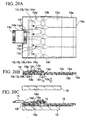
- FIGS.19A to 19C show the driver IC module in which an aluminum substrate is employed as the substrate on which the driver IC chips can be secured stably and which has a function as the earth wirings and a radiation operation.
- all wirings of the input portion and wirings of the output portion are formed by a sheet of flexible substrate 19, and the wirings of the input portion and the wirings of the output portion of the flexible substrate 19 are directly connected to a plurality of pad terminals 10a of the driver IC chip 10 by using the bumps, the anisotropic conductive film, or the conductive adhesive.
- the flexible substrate 19 has a multi-layered wiring structure at its input portion, and a plurality of wirings 19g are formed on the upper layer portion of the base film 19a and cross-wired to the lower layer portion side via through holes 19h.
- the wirings which are re-arranged on the lower layer portion side has a structure to contain input signal wirings 19i, low voltage power supply wirings 19j, high voltage power supply wirings 19k, and earth wirings 19m, respective wirings are input into four driver IC chips 10 in parallel.
- the output wirings are formed in the form of a single layer wiring structure by using only the wirings 19c of the lower layer portion.
- a covering film 19b is pasted on surfaces of the wirings 19g of the upper layer portion and the wirings 19i, 19j, 19k, 19m, 19c of the lower layer portion to insulate and protect them.
- Input terminals 19f are provided to the wirings 19g of the upper layer portion, and the FFC 14 connected to the external substrate is connected to the input terminals 19f by the soldering.
- Respective terminals of the input signal wirings 19i, the low voltage power supply wirings 19j, the high voltage power supply wirings 19k, and the earth wirings 19m, which are the wirings of the lower layer portion on the input side, as described above, are directly connected to corresponding pads of the driver IC chips 10 by using the bumps, the anisotropic conductive film, or the conductive adhesive. These terminals together with the terminals of the input portion are connected at the same time by the batch bonding.
- wirings and earth terminals 19p which are connected to the aluminum substrate 18 to apply the earth potential, are provided to the wirings of the lower layer portion on the input side of the flexible substrate 19.
- the earth terminals 19p are provided by opening a part of the covering film 19b to a predetermined size, and connected to the surface of the aluminum substrate 18 by the method described later and also connected to the corresponding pads 10a of the driver IC chip 10 by the batch bonding described above.
- the flexible substrate 19 and the aluminum substrate 18 are stuck to each other such that both fitting holes 19q, 18a coincide with each other.
- the back surface of the driver IC chip 10 may be tightly contacted by using the same adhesive as that employed to stick the flexible substrate 19.
- sticking to the back surface of the aluminum substrate 18 by the die bonding using the conductive adhesive is superior in the electrical stability and is ideal.
- the conductive adhesive is filled in the openings which expose the earth terminals 19p on the lower surface side of the flexible substrate 19 if the conductive adhesive is employed, connection between the earth terminals 19p and the aluminum substrate 18 can be facilitated.
- the connecting method in addition to the above conductive adhesive, the bumps, the anisotropic conductive film, or the like may be employed like the connection to the pad terminals 10a, or the soldering by using the dedicated solder material for aluminum material may be employed, or the pressure welding by using the high temperature and the high pressure may be employed.
- the input portion terminals 19f of the flexible substrate 19 are connected to the terminals 14d of the FFC 14 by the soldering, and then bypass chip capacitors 13a, 13b are provided between the power supplies and the ground by the soldering, whereby all assembling steps are completed.
- the driver IC packaging module shown in FIGS.19A and 19C since the mounting surface of the driver IC chip 10 on the aluminum substrate 18 and the exposed surfaces 19e of the output terminals 19c on the flexible substrate 19 can be set oppositely, the module can be easily fitted to the frame 4 and the heat radiation efficiency is excellent, like the above-mentioned embodiments.
- the method of connecting directly the aluminum substrate 18 to the earth pads of the driver IC chip 10 as the earth potential can be omitted according to the magnitude of the load of the display panel. That is, if the panel size is relatively small and the load current is small, the driver IC chip 10 is never affected by the bad influence such as noise, etc. Therefore, as shown in FIGS.20A to 20C, the above earth terminals 19p may be omitted in fabrication to reduce the cost.
- FIGS.20A to 20C the same references as those shown in FIGS.19A to 19C denote the same elements.
- FIGS.19A to 19C the structure using the flexible flat cable (FFC) 14 connected to the external circuits is shown in FIGS.19A to 19C.
- the upper layer portion wirings 19g, for example, of the input portion of the flexible substrate 10 are formed as the input terminals 19f by projecting outward from the input side end portion of the aluminum substrate 18, and thus also used as the input cables.
- the input terminals 19f of the flexible substrate 19 are connected to the bus substrate 8 via the connectors 7 shown in FIG.12.
- a flexible substrate 20 having all single layer wiring structure may be adopted in place of the flexible substrate 19 having the multi-layered wiring structure in the input portion shown in FIGS.19 and 21.
- the flexible substrate 20 is so constructed that all wirings are formed to be put between a base film 20a and a covering film 20b.
- the input portion wirings contain input signal wirings 20i, low voltage power supply wirings 20j, high voltage power supply wirings 20k, and earth wirings 20m, and input terminals 20f on the input end and connection terminals 20n on the output end are exposed from the covering film 20b.
- Output pottion wirings 20c have connection terminals 20d on the input end exposed from the covering film 20b side and output terminals 20e on the output end.
- connection terminals 20n, 20d on the output end and the input end are connected to the pads 10a of the driver IC chip 10 by the batch bonding respectively.
- earth terminals 20p to be earth-connected to an aluminum substrate 18 are provided in the neighborhood of the output terminals 20n of the input side and connected to the driver IC chips 10 via the aluminum substrate 18.
- the input terminals 20f of a flexible substrate 20 are used while being connected to the bus substrate 8 via the connectors 7.
- the multi-layered wiring structure in the input portion and the single layer wiring structure in the output portion of the flexible substrate 19 shown in FIGS.19 and 21 are fabricated separately on the separate flexible substrates, and then constructed by combining the separate flexible substrates together.
- the driver IC packaging module having the above configuration is fitted onto the chassis 4 under the same situation as that shown in FIG. 12. That is, since the back surface of the aluminum substrate 18 is fixed to the second beam member 3 by the wires so as to directly contact to the second beam member 3, the heat generated by the driver IC chips 10 can be radiated to the chassis 4 via the aluminum substrate 18 having the high thermal conductivity. In this case, the chassis 4 functions as a heat sink.
- the aluminum substrate 18 has a role as the earth plane 11 m in the first embodiment, and can be held at the earth potential via the chassis 4.
- the earth terminals 10p, 20p may be omitted like the case shown in FIG.20C.
- the driver IC packaging modules explained in FIG.19, FIG.20, FIG.21 and FIG.22 have the structure in which the electrical connection to the aluminum substrate 18 which also acts as the earth wirings is connected by using the earth terminals 19p, 20p provided in the flexible substrates 19, 20.
- a structure in which the earth pads 10c on the driver IC chip 10 and the aluminum substrate 18 are connected by the wire bonding may be employed.
- FIGS.23A to 23C the electrical connection relationship between the flexible substrate 19 and the driver IC chips 10 and the input flat cable 14 is constructed substantially similarly to that in FIG.19, and the similar aluminum substrate 18 is also equipped.
- opening portions 19r for connecting the earth connection are provided in areas of the flexible substrate 19, which are located on both sides of the input portion of the driver IC chip 10.
- the opening portions 19r are provided to assure the lowest minimum areas for connecting the earth pad terminals 10c, which are provided by two on both side locations of the input portion of the driver IC chip 10, and the surface of the aluminum substrate 18 via the wire bonding, and thus are provided at eight locations in total for four driver IC chips 10.
- terminals of the flexible substrate 19 and the corresponding pad terminals of the driver IC chip 10 are connected by the batch bonding like FIG.19, then the protection resin is coated on these connection portions to protect them, and then both are pasted onto the aluminum substrate 18, as shown in FIG.23C.
- connection to the aluminum substrate 18 can be completed by connecting the earth pad terminals of the driver IC chip 10, which are exposed from the opening portions 19r of the flexible substrate 19, and the surface of the aluminum substrate 18 individually by the wire bonding.
- the assembling can be finished by soldering the chip capacitors 13a, 13b and the input flat cable 14.
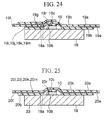
- FIGS.24 and 25 correspond to the foregoing structures shown in FIGS.21 and 22 respectively, and show examples in which the wire bonding connection method similar to those in FIGS.21 and 22 is applied.
- connection to the aluminum substrate 18 serving as the earth wiring can be provided without fail and also the earth connection can be provided more firmly.
- the number of wire bonding for connecting the earth pad terminals 10c of the driver IC chip 10 and the surface of the aluminum substrate 18, as mentioned above, may be reduced in the small size and light load display panel, and thus the lower cost can be achieved.
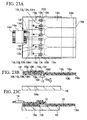
- a driver IC packaging module will be explained in which the input portion wirings and the output portion wirings, which have the similar structure to those explained in the third embodiment and the fourth embodiment, are formed of the flexible substrate, and a part or all of the power supply wiring layers are provided on the printed substrate side.
- both the input portion wirings and the output portion wirings are formed of a sheet of flexible substrate 22, and respective wirings and corresponding pads 10a of the driver IC chip 10 are directly connected by using the bumps, the anisotropic conductive film, or the conductive adhesive.
- the high voltage power supply wirings and a part or all of the earth wirings are provided on the printed substrate 21 side.
- FIGS.26A to 26C such a structure is adopted that all the high voltage power supply wirings and most of the earth wirings are provided on the printed substrate 21 side and a part of the earth wirings is also provided on the flexible substrate 22 side.
- a structure of the printed substrate 21 is constructed by forming an earth plane 21h made of the copper foil on the lower surface (back surface) and then extending the earth plane 21h to input terminals 21c, which are arranged on the input terminal portions, via through holes 21i on the input portion side and via the earth wirings 21d on the upper surface (front surface).
- the earth plane 21h is also connected to the earth pattern 21f formed on the upper surface via the through hole 21j (thermal via) directly below the driver IC chip 10. This earth pattern 21f is also connected electrically to the earth wirings 21d and is directly coupled to the input terminal 21c side.
- the high voltage power supply plane 21g is formed in areas of the upper surface of the printed substrate 21 on the output end side by patterning the copper foil. This high voltage power supply plane 21g is extended to the input end terminals 21c via the high voltage power supply wirings 21e.
- lands (areas) in which the bypass capacitor 13b described later is mounted to connect the earth wirings 21d and the high voltage power supply wirings 21e are also provided in the input side area of the upper surface of the printed substrate 21.
- the flexible substrate 22 has a multi-layered wiring structure at its input portion, and a plurality of wirings 19g are cross-wired by the upper layer portion wirings 22g and the lower layer portion wirings 22c, which sandwich the base film 22a therebetween, and input into four driver IC chips 10 in parallel respectively.
- the output wirings are formed in the form of the single layer wiring structure by using only the wirings 22c of the lower layer portion.
- the input terminals 22f to which the FFC 14 connected to the external devices is soldered are provided to the upper layer portion wirings 22g and, as previously described, respective wirings of the input signal wirings, the low voltage power supply wirings, and the earth wirings are input into the wirings 22g. These input wirings are cross-wired to the lower layer portion wiring side via the through holes 22h provided in the base film 22a.
- the input signal wirings 22i, the low voltage power supply wirings 22j, and the earth wirings 22m are contained in the lower layer portion wirings. Respective terminals and the corresponding terminals of the driver IC chips 10 are directly connected by using the bumps, the anisotropic conductive film, or the conductive adhesive.
- connection terminals 22d for the output wirings are provided on the output portion side of the lower layer portion wirings. Respective terminals and the corresponding terminals of the driver IC chips 10 are directly connected by using the bumps, the anisotropic conductive film, or the conductive adhesive. These terminals together with the terminals of the input portion are connected at the same time by the batch bonding.
- wirings and the high voltage terminals 22s which are connected to high voltage power supply wirings 21e or a high voltage power supply plane 21g provided on the printed substrate 21, are provided in the intermediate portion between the input portion wirings and the output portion wirings of the lower layer portion wirings of the flexible substrate 22. Also, wirings and the earth terminals 22p, which are connected to earth wirings 21d or an earth plane 21h provided on the printed substrate 21, are provided therebetween.
- the high voltage terminals 22s and the earth terminals 22p are exposed from the printed substrate 21 side by opening a part of the covering film 22b to a predetermined size. They are connected to respective wirings or the pattern on the surface of the printed substrate 21 by the later-described method, and connected at the same time when the above batch bonding is applied to the corresponding pad terminals 10a of the driver IC chip 10.
- the flexible substrate 22 and the printed substrate 21 are stuck to each other such that both fitting holes 22q, 21b coincide with each other.
- the back surface of the driver IC chip 10 may be tightly contacted by using the same adhesive as that employed to stick the flexible substrate 22.
- sticking to the earth patterns 21f on the surface of the printed substrate 21 by the die bonding using the conductive adhesive is superior in the electrical stability and is ideal.
- the electrical connection between the high voltage terminals 22s and the earth terminals 22p in the intermediate portion of the above flexible substrate 22 and the printed substrate 21 is conducted together with this adhesion.
- the connecting method in addition to the above conductive adhesive, the bumps, the anisotropic conductive film, or the like may be employed like the connection to the pad terminals 10a, otherwise the soldering by using the dedicated solder material for aluminum material may be employed, otherwise the pressure welding by using the high temperature and the high pressure may be employed.
- terminals of the flat cable 14 is soldered.
- the input signal wirings, the low voltage power supply wirings, and a part of earth wirings are connected to terminal portions of the input portion wirings 22f of the flexible substrate 22, then remaining part of the earth wirings are also connected to the earth terminals, which are connected to the earth wirings 21d on the printed substrate 21 side, as described above, and then the high voltage power supply wirings are directly connected to the high voltage power supply terminals which are connected to the high voltage power supply wirings 21e on the printed substrate 21 side.
- the chip-like bypass capacitor 13a is soldered onto the lands which are provided to the low voltage power supply wirings 22j and the earth wirings 22m on the flexible substrate 22, and also the chip-like bypass capacitor 13a is soldered onto the lands which are formed on the high voltage power supply wirings 21e and the earth wirings 21d on the flexible substrate 21 and exposed from the opening portions of the flexible substrate 22, whereby all assembling steps can be completed.
- the driver IC packaging module shown in FIG.26 since the mounting surface of the driver IC chip 10 on the aluminum substrate 18 and the exposed surfaces 22e of the output terminals on the flexible substrate can be set In the opposite direction, the module can be easily fitted to the frame 4 and thus the heat radiation efficiency is excellent, like the above-mentioned embodiments.
- the flat cable 14 is connected to the bus substrate 8 via the connectors 7.
- FIGS.28A to 28C show a configuration in which a straight-type substrate-to-substrate connecting connector 15 is employed instead of the input flat cable 14.
- the connector 15 is mounted on the lower surface side of the printed substrate 21 and soldered such that connecting pins 15b are projected from the upper surface side of the printed substrate 21.
- the connecting pins 15b for the input signal wirings, the low voltage power supply wirings, and a part of earth wirings are soldered to the terminals 22f of the flexible substrate 22, and the connecting pins 15b for the high voltage power supply wirings and the remaining part of the earth wirings are soldered to the terminals 21c on the printed substrate 21 side.
- the advantages similar to that in FIG.26 can be achieved by connecting the module to the bus substrate 8 via the connector 15.
- the single layer structure may be used. Such single layer structure is shown in FIGS.29A to 29C.
- the input portion of the flexible substrate 23 is also used commonly as the input cable by such that such input portion of the flexible substrate 23, for example, the upper layer portion wirings 23i, 23j, 23m are projected outwardly from the input side end portion of the flexible substrate 23.
- top end portion terminals 23f are connected to the bus substrate 8 via the connector 15.
- the flexible substrates 22, 23 are shown to have such a structure that the input portion and the output portion are formed as a sheet of common substrate. However, the input portion and the output portion are formed as other separate substrates respectively, and then the flexible substrates 22, 23 can be constructed by combining the separate substrates together.
- the connection between the earth pattern 21f and the high voltage power supply pattern 21g on the printed substrate 21 and the corresponding pad terminals 10a of the driver IC chips 10 is accomplished by utilizing the earth terminals 23p and the high voltage terminals 23s provided on the flexible substrate 23 side.
- the present invention is not limited to such connection, the earth pattern 21f, etc. and the corresponding pad terminals 10a can be connected by using the wire bonding, as shown in FIGS.30A to 30C, for example.
- references 25a, 25b,..., shown in FIGS.30A to 30C denote identical elements which correspond to the references 22a, 22b,..., shown in FIGS.26A to 26C.
- opening portions 25r which connect the earth pattern 21f and the high voltage power supply plane 21g on the printed substrate 21 and the corresponding pads 10a of the driver IC chip 10, are provided in areas of the flexible substrate 25, which are located on both side portions of the area, in which the driver IC chip 10 is arranged, of the flexible substrate 25.
- the wire bonding between the earth pattern 21f and the high voltage power supply plane 21g on the printed substrate 21 and the corresponding pads 10a of the driver IC chip 10 can be carried out by providing the opening portions 25r.
- the driver IC packaging module having the above configuration is fitted onto the chassis 4 under the same situation as that shown in FIG. 12. That is, since the earth layer 21h on the back surface of the printed substrate 21 are secured to the second beam member 3 by the vires so as to directly contact to the second beam member 3, the heat generated by the driver IC chips 10 can be radiated to the chassis 4. In this case, the chassis 4 functions as the heat sink.
- FIGS.31A to 31E a structure is adopted in which the lower surfaces of the earth planes 11m, 21h are lined with a metal plate 30 such as an aluminum plate having high thermal conductivity.
- the metal plate 30 is tightly contacted to the earth planes 11m, 21h by the thermal conductive adhesive, or the conductive adhesive.
- the module shown in FIG.31A corresponds to the module shown in FIG.9B
- the module shown in FIG.31B corresponds to the module shown in FIG.17C
- the module shown in FIG.31C corresponds to the module shown in FIG.18C
- the module shown in FIG.31D corresponds to the module shown in FIG.26C
- the module shown in FIG.31E corresponds to the module shown in FIG.29C.
- these metal plates 30 are fitted onto the beam members 3, 3b of the chassis 4 shown in FIGS.12 and 14 and thus the heat being transmitted to the metal plates 30 can be radiated to the chassis 4.
- connection between the flexible flat cable (FFC) and the bus substrate is carried out via the connector.
- the flexible flat cable and the bus substrate are connected by the soldering.
- an insulating protection film e.g., a resist film for covering various wirings, various planes, etc. is formed on the upper surface and the lower surface of the printed substrate explained in the first, second, fifth to seventh embodiments.
- the insulating protection film is removed partially from the electrical connection portions between various wirings, various planes, etc. on the printed substrate and the flexible substrate, the FFC, the driver IC chip s10, etc.
- a part or all of the insulating protection film is removed from the contact areas between the printed substrate and the chassis.
- a structure to intersect a plurality of beam members is adopted as the chassis structure to which the driver IC packaging module is fitted.
- the present invention is not limited to such structure.
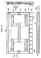
- a structure shown in FIG.32 may be employed in place of the above embodiments.
- a chassis 55 of the PDP device shown in FIG.32 has a flat metal plate 55a.
- the display panel is adhered to a front surface of the metal plate 55a, and beam members 55b, 55c having a hat-shaped sectional shape are fitted in parallel to plural locations of a back surface of the metal plate 55a to reinforce the metal plate 55a.
- a lower step portion 56a of a metal beam 56 which has a Z-shaped sectional shape (step-like shape) is fixed to one side portion of the back surface of the metal plate 55a by the caulking using TOX, HENROBRIVETS, etc., and the driver IC packaging module M0 is fitted to an upper step portion 56b of the metal beam 56.
- a plurality of driver mounting substrates 57a to 57c, power supply substrate 57c, etc. are fitted between the beam members 55b and between the beam member 55b and the beam 56 to cross over them.
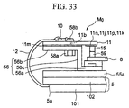
- driver IC packaging module M0 If the structure shown in FIG.10 is adopted as the driver IC packaging module M0, such driver IC packaging module M0 is fitted onto the upper step portion 56b of the metal beam 56 in the state shown in FIG 33.
- the upper step portion 56b of the metal beam 56 which is fitted to the metal plate 55a and has the Z-shaped sectional shape is floated from the metal plate 55a, and then the printed substrate 11 shown in FIG.10 is mounted on the upper step portion 56b and held by the screws. More particularly, press nuts 58a are press-fitted to the back side of the upper step portion 56b of the metal beam 56, then the fitting holes 11b of the printed substrate 11 are aligned with the press nuts 58a, and then vires 58b are screwed in the press nuts 58a via the fitting holes 11b.
- the earth planes 11m on the lower surface of the printed substrate 47 is brought into contact to the upper surface of the upper step portion 56b of the metal beam 56, while signal wirings 50e, power supply wirings 50f on the lower surface are positioned in areas which are out of the metal beam 56 to prevent short-circuit between the earth planes 11m and them.
- the wirings 11n, 11j, 11p, 11k of the lower surface of the printed substrate 11 are connected to the bus substrate 8 via the connectors 15.
- the flexible wirings 12 connected to the printed substrate 11 are curved and then connected to the electrodes 5a on the rear glass substrate 102 of the display panel 5.
- the heat generated from the driver IC chips 10 can be radiated to the outside via the printed substrate 11, the earth planes 11m, and the metal beam 56.
- the earth planes 11m can be held at the earth potential via the metal beam 56.
- chassis 55 having the above-mentioned structure can achieve the effect as the heat radiation and thermal diffusion plane for not only the heat generated from the driver IC chips 10 but also the heat generated from the display panel 5 and other driver circuit substrates. Therefore, since the thermal characteristic of the overall PDP device can be improved and the mechanical strength can be held by the metal beam 56, the thin structure having the sufficient mechanical strength can be accomplished.
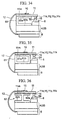
- the sectional shape of the metal beam 56 is not limited to the Z-shape sectional shape, and may have a structure described in the following.
- a beam 60 has a U-shaped sectional shape (groove shape).
- the beam 60 has an upper portion 60a and a lower portion 60b which oppose to each other.
- the lower portion 60b is secured to the chassis 4, 55 side, and the printed substrate 11 is fitted onto the upper portion 60a.
- the printed substrate 11 is fixed to the beam 60 by the screws (not shown), etc. such that only the earth planes 11m on the lower surface of the printed substrate 11 can come into contact to the beam 60.
- the metal beam 56 having the Z-shaped sectional shape shown in FIG.33 and the beam 60 having the U-shaped sectional shape shown in FIG.34 can be formed by folding the flat metal plate respectively.
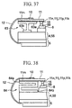
- a beam 61 having a square-pipe sectional shape shown in FIG.35 there are a beam 61 having a square-pipe sectional shape shown in FIG.35, a beam 62 having an H-shaped sectional shape shown in FIG.36, a beam 63 having a T-shaped sectional shape shown in FIG.37, a beam 64 having a lip Z-shaped sectional shape shown in FIG.38, etc.
- upper portion 62a to 64a to which the printed substrate 47 is fitted and lower portions 62b to 64b which are fitted onto the chassis 14, 55 are present.
- the upper portion 62a to 64a and the lower portions 62b to 64b are directed in parallel mutually.
- the beams 61 to 64 shown FIGS.35 to 38 are formed by the extrusion. Lower portions 61b to 64b of these beams 61 to 64 are secured to the chassis 4, 55 by the caulking using TOX, HENROBRIVETS, etc.
- the printed substrate 11 is fixed to upper portions 61a to 64a of the beams 61 to 64 by the press nuts (not shown) and the screws (not shown).
- the earth planes 11m on the lower surface of the printed substrate 11 come directly into contact to the upper portions 61a to 64a of the beams 61 to 64.
- FIG.39 shows a structure in which a radiation fin 65 is fitted onto the lower surface of the upper step portion 56b of the beam which has the Z-shaped sectional shape.
- Countersinks (not shown) for flat countersink machine screws are formed in the upper step portion 56a, and screwed holes (not shown) are formed in the radiation fin 65 at locations corresponding to the countersinks. Then, the screws are fitted into the screwed holes of the radiation fin 65 through the countersinks in the upper step portion 56b of the beam 56.
- cross- recessed pan-head machine screws which are widely used normally are used as the screws, head portions are protruded from the upper surface. Therefore, the earth patterns on the printed substrate cannot be brought into contact to the upper surface, and thus it is indispensable to use the pan-head machine screws.
- the better heat radiation effect can be achieved rather than the case where only the beam 56 is used.
- FIG.40 shows a structure in which comb-like projections 66b are formed on the lower surface of the upper portion 66a of the beam 66 which has the Z-shaped sectional shape.
- the projections 66b and the beam 66 are formed integrally by the extrusion.
- the comb-like projections 66b has the same heat radiation effect as the radiation fin 65 in FIG.41, nevertheless the time and labor can be saved in manufacturing because the screw fitting can be omitted.
- the lower step portion 66c of the beam 66 is secured to the chassis 4, 55.
- FIG.41 shows a structure in which a part of the beam 67 which has the Z-shaped sectional shape is folded at an acute angle.
- On intermediate portion 67c for connecting the upper step portion 67a and the lower step portion 67b is set vertically relative to the lower step portion 67b, and the upper step portion 67a is folded to have an acute angle less than 90 degree relative to the intermediate portion 67c.
- the printed substrate 11 shown in FIG.9 is fitted to the upper surface of the upper step portion 67a in the situation that the lower step portion 67b is secured to the chassis 14, 55, the printed substrate 11 is inclined toward the display panel side according to the inclination of the upper step portion 67a such that the flexible substrate 12 on the output side of the driver IC packaging module comes close to the display panel 5.
- the chassis of the PDP device and the beam on which the driver IC packaging module is mounted are formed integrally.
- FIG.42 is a rear view and a side view showing the PDP device according to the tenth embodiment of the present invention.
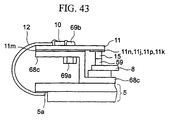
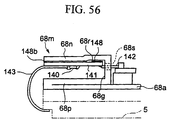
- a chassis 68 used in the PDP device has a metal plate 68a which is pasted on the whole back surface of the display panel 5, and a plurality of beam members 68b having the hat-like sectional shape are secured in parallel to the rear surface of the metal plate 68a. Then, both side portions of the metal plate 68a are folded like the Z-shaped sectional shape, and the upper step portion of the Z-shaped sectional shape serves as the module mounting portion 68c to which the printed substrate 11 of the driver IC packaging module shown in FIG.10, for example, is mounted.
- the printed substrate 47 of the driver IC packaging module M0 is secured onto the top surface of the module mounting portion 68c by the screws.
- the press nuts 69a are press-fitted to the module mounting portion 68c from the back side to mate with the fitting holes 11b of the printed substrate 11 of the driver IC packaging module, then the screws 69b are fitted into the press nuts 69a through the fitting holes 11b of the printed substrate 11.
- connection between the flexible substrate 12 of other driver IC packaging modules and the display panel 15 and the connection between the wirings 11n, 11j, 11p, 11k on the input side of the printed substrate 11 and the bus substrate 8 are conducted by the same method as those in the above embodiments.
- the module mounting portion 68c constituting a part of the chassis 68 can achieve the effect as the heat radiation and thermal diffusion plane for not only the heat generated from the driver IC chips 10 but also the heat generated from the display panel 5 and other driver circuit substrates and therefore the thermal characteristic of the overall PDP device can be improved.
- the metal plate 68a and the module mounting portion 68c are formed integrally while holding the mechanical strength, the thinner structure than those in the above embodiments can be accomplished.
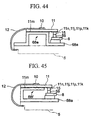
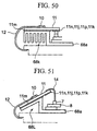
- the folding shape of the metal plate 68a to form the module mounting portion 68c on both sides of the metal plate 68a constituting the chassis 68 various shapes explained in the sixth embodiment may be adopted in addition to the Z-shaped sectional shape. That is, the hat-shaped module mounting portion 68e shown in FIG.44, the U-shaped module mounting portion 68f shown in FIG.45, the square- shaped module mounting portion 68g shown in FIG.46, the H-shaped module mounting portion 68h shown in FIG.47, the lip Z-shaped module mounting portion 68i shown in FIG.48, the Z-shaped module mounting portion 68j shown in FIG.49 in which the heat radiation fin 65 is arranged on the back surface of the fitting surface of the printed substrate 47, the Z-shaped comb-type module mounting portion 68k having the shown in FIG.50, and the acute Z-shaped module mounting portion 68l shown in FIG.51 may be employed. Since the fitting of the driver IC packaging module M0 onto these module mounting portions 68e to 68k is similar to
- the printed substrates having the structure in which various conductive wirings and various conductive planes are formed on the upper surface and the lower surface and are connected via the through holes are employed, or the printed substrates having the multi-layered wiring structure are employed.
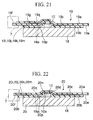
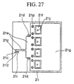
- driver IC packaging modules having such structures such a structure may be employed that a driver IC packaging module having a new COB structure, as shown in FIG.52, is fitted onto the chassis 4 of the display panel.
- an intermediate earth pattern 47a and an intermediate high voltage power supply pattern 47b are formed in the inside of the printed substrate 47.
- the intermediate earth pattern 47a is connected to a high voltage power supply pattern 47d on the upper surface via a first through hole 47c in the printed substrate 47.
- the intermediate high voltage power supply pattern 47b is formed on the output side of a die bonding pattern 47e which is formed in a central area of the upper surface of the printed substrate 47, and is connected to a high voltage pad 10p of the driver IC chip 10 on the die bonding pattern 47e by the wire bonding.
- a second through hole 47f is formed in the inside of the printed substrate 47.
- the die bonding pattern 47e and the earth plane 47g on the lower surface of the printed substrate 47 are connected electrically mutually via the second through hole 47f and the intermediate earth pattern 47a.
- the die bonding pattern 47e is connected to the earth pads 10c on the driver IC chip 10 by the wire bonding.
- the first through hole 47c and an opening 47h are formed in the earth plane 47g, whereby short-circuit between the earth plane 47g and the intermediate high voltage power supply pattern 47b can be prevented.
- first signal wirings 49i, first high voltage power supply wirings 49i, first earth wirings 49k, and first low pressure power supply wirings 49m are formed on the input side of the upper surface of the printed substrate 47. These wirings are connected to second signal wirings 49q, second high voltage power supply wirings 49r, second earth wirings 49s, and second low pressure power supply wirings 49t on the lower surface of the printed substrate 47 via through holes 49n, 49p.
- Wirings 51a of the FFC 51 are directly connected to respective input terminals of the first signal wirings 49i, the first high voltage power supply wirings 49i, the first earth wirings 49k, and the first low pressure power supply wirings 49m.
- the pads 10a of the driver IC chip 10 are connected to their output terminals by the wire bonding.
- the FFC 51 is connected to the bus substrate 8 via the connectors 7.
- output wirings 49u are provided on the output end side of the printed substrate 47, and input end areas of the wirings 53a of the flexible substrate 53 are connected to the upper surfaces of the output wirings 49u via the conductive adhesive.
- the wirings 53a of the flexible substrate 53 are put between first and second insulating films 53b, 53c, and input ends and output ends of the wirings 5a are exposed in the same direction. That is, the input ends and the output ends of the wirings 5a are directed oppositely to the driver IC chip 10 mounting surface of the printed substrate 47.
- the output wirings 52 and the pads 10a of the driver IC chip 10 are connected by the wire bonding.
- the foregoing driver IC packaging module has the new COB structure that the wirings 49q, 49r, 49s, 49t for supplying the input signal, or the power supply voltages, the earth voltage are provided in the input signal portion side of the lower surface of the printed substrate 47, and only the earth plane 49g is provided in the output signal portion.
- the fitting of the driver IC packaging module onto the chassis 4 of the PDP device shown in FIG.11 is performed by fixing the module by the vires 6 as shown in FIG.53, and then adhering the earth plane 49g to the chassis 4 via the conductive adhesive, etc. so as to face the wirings 49q, 49r, 49s, 49t to the concave portions 3a of the beam member 3 in a non-contact condition.
- the heat generated by the driver IC chip 10 can be discharged to the chassis 4 via the printed substrate 47 having the high thermal conductivity and the earth plane 47g.
- the earth plane 47g on the lower surface of the printed substrate 47 can be kept at the earth potential via the chassis 4.
- the wirings are formed as the three-dimensional wiring structure by using patterns on the upper surface, the lower surface, and the intermediate surface of the printed substrate and the through holes, the printed substrate 47 can be secured stably to the chassis 4 with reducing the wiring area on the input side and increasing the contact area between the printed substrate 47 and the chassis 4.
- the driver IC module having the structure in which the driver IC mounting surface of the printed substrate and the exposed direction of the output wiring ends of the flexible substrate are directed oppositely is employed.
- the driver IC module having the COM structure shown in FIG.5B may be fitted to the back surface of the upper step portion 70a of the Z-shaped beam 70 shown in FIG.54 or it may be fitted to the back surfaces of the upper surfaces 71a, 72a of the U-shaped beams 71, 72 shown in FIGS.55 and 56.
- the beam 70 shown in FIG.54 is prepared separately to the chassis 4, 55 shown in FIGS.10 and 32, and is formed integrally with the chassis 68 by fixing the lower portion 70c to the chassis 4, 55 by the caulking, etc. or by folding side portions of the metal plate 68a constituting the chassis 68 shown in FIG.42.
- the beam 70 consists of an upper portion 70a, a lower portion 70b, and a supporting portion 70c for connecting them.
- the concave portion 70e is formed in the area, which is close to the supporting portion 70c, of the back surface of the upper portion 70a.
- a printed substrate 141 is fixed to the beam by the screws, etc. in the situation that only an earth pattern 148 shown in FIG.5B comes into contact to the beam on the back surface of the upper portion 70a.
- Wirings 148a on the input side of the printed substrate 141 are arranged to face to the concave portions 70e in the non-contact state.
- the wirings of the FFC 142 are connected to the bus substrate 8 by the connectors 7 via the through holes 70d formed in the supporting portion 70c of the beam 70.
- the beam 71 consists of an upper portion 71a and a lower portion 71b which oppose to each other at a distance, and a supporting portion 71c for connecting them. Then, the concave portion 71e is formed in the area, which is close to the supporting portion 71c, of the back surface of the upper portion 71a. Then, the printed substrate 141 is fixed to the upper portion 71a of the beam 71 by the screws, etc. in the situation that only an earth pattern 148b shown in FIG.5B comes into contact to the beam 71 on the back surface of the upper portion 71a.
- the wirings 148a on the input side of the printed substrate 141 are arranged to face to the concave portions 71e in the non-contact state. Then, the wirings of the FFC 142 are connected to the bus substrate 8 by the connectors 7 via the through holes 71d formed in the supporting portion 71c of the beam 71.
- the U-shaped beam 68m shown in FIG.55 is formed integrally with the chassis 68 by folding side portions of the metal plate 68a constituting the chassis 68 shown in FIG.42.
- the beam 68m consists of an upper portion 68n and a lower portion 68p which oppose to each other at a distance, and a supporting portion 68g for connecting them. Then, the concave portion 68r is formed in the area, which is close to the supporting portion 68g, of the back surface of the upper portion 68n. Then, the printed substrate 141 is fixed to the upper portion 68n of the beam 68m by the screws, etc. in the situation that only the earth pattern 148b shown in FIG.5B comes into contact to the beam 68m on the back surface of the upper portion 68n.
- the wirings 148a on the input side of the printed substrate 141 are arranged to face to the concave portions 68r in the non-contact state. Then, the wirings of the FFC 142 are connected to the bus substrate 8 by the connectors 7 via the through holes 68s formed in the supporting portion 68g of the beam 68m.
- the heat generated by the driver IC chip 10 mounted on the upper surface of the printed substrate 141 can be radiated to the beam 70, 71 or the beam 68m via the printed substrate 141, the earth pattern 148b, and then the heat transmitted to the beam 70, 71 or the beam 68m can be radiated the chassis 4, 55, 68.
- one end portion, which are connected to the display panel electrodes, of the wirings which are passed through the flexible substrate fitted to an area located in the neighborhood of one end of the driver IC chip mounting surface is exposed in the opposite direction to the driver IC chip mounting surface. Therefore, it is possible to direct the driver IC chip mounting surface to the rear surface side and connect one end portion of the electrodes of the flexible substrate to electrodes on a front surface of the display panel by bending the flexible substrate.
- a structure which brings the back surface (surface opposite to the driver IC chip mounting surface) of the module substrate into contact to the surface of the chassis can be achieved easily, the chassis per se can be ready to be utilized as the heat radiation plate for the heat generated by the substrate, and thus a structure of the flat display device which can improve the thermal characteristic of the module and can be installed compactly can be achieved.
- the mechanical strength can be maintained by attaching the beam-like structure to the chassis on the rear surface of the display panel or forming a part of the chassis itself as the beam-like structure, and also the substrate surface of the driver IC packaging module can come into contact into the flat plate surface of this beam-like structure. Therefore, the heat generated from the driver IC chip can be diffused to the chassis via the beam, and thus the built-in packaging structure whose thickness is small and whose thermal characteristic can be improved as a whole can be achieved while holding the original mechanical strength of the chassis as it is.
- the chassis is formed of the flat metal plate having a size to cover substantially the overall rear surface side of the panel
- the chassis is formed to have a wide area
- such a chassis can have the effect as the heat radiation and thermal diffusion plate for not only the heat generated by the driver IC chip but also the heat generated by the display panel and other driver circuit substrates. Therefore, the thermal characteristic of the overall device can be improved and the mechanical strength can be still maintained by attaching the beam. As a result, a thin flat display device having sufficient mechanical strength can be achieved.
Landscapes
- Physics & Mathematics (AREA)
- Engineering & Computer Science (AREA)
- Nonlinear Science (AREA)
- General Physics & Mathematics (AREA)
- Optics & Photonics (AREA)
- Crystallography & Structural Chemistry (AREA)
- Chemical & Material Sciences (AREA)
- Thermal Sciences (AREA)
- Mathematical Physics (AREA)
- Microelectronics & Electronic Packaging (AREA)
- Plasma & Fusion (AREA)
- Computer Hardware Design (AREA)
- Theoretical Computer Science (AREA)
- Devices For Indicating Variable Information By Combining Individual Elements (AREA)
Applications Claiming Priority (2)
| Application Number | Priority Date | Filing Date | Title |
|---|---|---|---|
| JP18637399 | 1999-06-30 | ||
| JP11186373A JP2001013883A (ja) | 1999-06-30 | 1999-06-30 | ドライバic実装モジュール及びそれを使用した平板型表示装置 |
Publications (2)
| Publication Number | Publication Date |
|---|---|
| EP1065720A2 true EP1065720A2 (de) | 2001-01-03 |
| EP1065720A3 EP1065720A3 (de) | 2007-05-23 |
Family
ID=16187260
Family Applications (1)
| Application Number | Title | Priority Date | Filing Date |
|---|---|---|---|
| EP00303447A Withdrawn EP1065720A3 (de) | 1999-06-30 | 2000-04-25 | Treiber-IC-Modulgehäuse und Flachbildschirm damit |
Country Status (5)
| Country | Link |
|---|---|
| US (1) | US6407508B1 (de) |
| EP (1) | EP1065720A3 (de) |
| JP (1) | JP2001013883A (de) |
| KR (1) | KR100549752B1 (de) |
| TW (1) | TW525117B (de) |
Cited By (7)
| Publication number | Priority date | Publication date | Assignee | Title |
|---|---|---|---|---|
| US6703702B2 (en) | 2001-07-30 | 2004-03-09 | Fujitsu Hitachi Plasma Display Limited | IC chip mounting structure and display device |
| EP1589576A3 (de) * | 2004-04-20 | 2006-03-15 | Fujitsu Hitachi Plasma Display Limited | Wärmeableitung einer Steuerschaltung für eine Plasmaanzeigetafel |
| US7443681B2 (en) * | 2005-01-22 | 2008-10-28 | Samsung Sdi Co., Ltd. | Heat dissipator for display apparatus and plasma display apparatus including the heat dissipator |
| EP2058695A1 (de) * | 2007-10-30 | 2009-05-13 | Fujitsu Limited | Verfahren zur Herstellung einer Anzeigeeinheit |
| EP1699066A3 (de) * | 2005-03-03 | 2009-12-09 | LG Electronics Inc. | Anzeigevorrichtung und flexibler Träger |
| EP2175703A1 (de) | 2008-10-08 | 2010-04-14 | Samsung SDI Co., Ltd. | Plasmaanzeigevorrichtung |
| US10120410B2 (en) | 2012-09-03 | 2018-11-06 | Semiconductor Energy Laboratory Co., Ltd. | Display device and electronic device |
Families Citing this family (68)
| Publication number | Priority date | Publication date | Assignee | Title |
|---|---|---|---|---|
| JP3886091B2 (ja) * | 2000-03-21 | 2007-02-28 | パイオニア株式会社 | フラットパネル型表示装置及びその製造方法 |
| JP2002117920A (ja) * | 2000-10-06 | 2002-04-19 | Fujitsu Hitachi Plasma Display Ltd | プラズマディスプレイ装置 |
| JP4786037B2 (ja) * | 2001-01-23 | 2011-10-05 | パナソニック株式会社 | 表示装置 |
| JP3774858B2 (ja) * | 2001-04-07 | 2006-05-17 | 大林精工株式会社 | 液晶表示装置とその駆動方法 |
| JP2002341785A (ja) * | 2001-05-11 | 2002-11-29 | Fuji Electric Co Ltd | ドライバic実装モジュール |
| JP4528795B2 (ja) * | 2001-07-30 | 2010-08-18 | 日立プラズマディスプレイ株式会社 | プラズマディスプレイ装置およびフラットディスプレイ装置 |
| JP4839244B2 (ja) * | 2001-07-30 | 2011-12-21 | 日立プラズマディスプレイ株式会社 | プラズマディスプレイ装置およびフラットディスプレイ装置 |
| JP4832334B2 (ja) * | 2001-07-30 | 2011-12-07 | 日立プラズマディスプレイ株式会社 | プラズマディスプレイ装置 |
| US6700315B2 (en) * | 2001-08-03 | 2004-03-02 | Samsung Sdi Co., Ltd. | Plasma display device having efficient heat conductivity |
| JP4562963B2 (ja) * | 2001-08-16 | 2010-10-13 | 株式会社日立製作所 | 液晶表示装置 |
| KR100429856B1 (ko) * | 2001-11-15 | 2004-05-03 | 페어차일드코리아반도체 주식회사 | 스터드 범프가 있는 웨이퍼 레벨 칩 스케일 패키지 및 그 제조 방법 |
| KR100846771B1 (ko) * | 2002-03-11 | 2008-07-16 | 삼성전자주식회사 | 플라즈마 표시장치 |
| KR100480174B1 (ko) * | 2002-08-23 | 2005-04-06 | 엘지전자 주식회사 | 플라즈마 디스플레이 패널의 구동장치 및 그의 제조 방법 |
| JP4207507B2 (ja) * | 2002-09-03 | 2009-01-14 | パナソニック株式会社 | プラズマディスプレイ装置 |
| US20040191955A1 (en) * | 2002-11-15 | 2004-09-30 | Rajeev Joshi | Wafer-level chip scale package and method for fabricating and using the same |
| US20050012225A1 (en) * | 2002-11-15 | 2005-01-20 | Choi Seung-Yong | Wafer-level chip scale package and method for fabricating and using the same |
| JP4269700B2 (ja) * | 2003-01-24 | 2009-05-27 | ソニー株式会社 | 表示装置 |
| KR100615174B1 (ko) * | 2003-10-14 | 2006-08-25 | 삼성에스디아이 주식회사 | 플라즈마 표시장치 |
| KR100627382B1 (ko) | 2003-10-23 | 2006-09-22 | 삼성에스디아이 주식회사 | 드라이버 ic 방열구조를 갖는 플라즈마 디스플레이 장치 |
| KR100570645B1 (ko) | 2003-10-23 | 2006-04-12 | 삼성에스디아이 주식회사 | 드라이버 ic 방열구조를 갖는 플라즈마 디스플레이 장치 |
| KR100683661B1 (ko) * | 2003-11-25 | 2007-02-20 | 삼성에스디아이 주식회사 | Tcp의 방열 구조 및 이를 구비하는 플라즈마디스플레이 장치 |
| KR100669700B1 (ko) * | 2003-11-28 | 2007-01-16 | 삼성에스디아이 주식회사 | 방열 성능이 개선된 플라즈마 표시장치 조립체 |
| KR100637149B1 (ko) | 2004-02-20 | 2006-10-20 | 삼성에스디아이 주식회사 | 플라즈마 디스플레이 장치 |
| KR100637151B1 (ko) * | 2004-02-21 | 2006-10-23 | 삼성에스디아이 주식회사 | 플라즈마 디스플레이 장치 |
| JP2005331945A (ja) * | 2004-05-18 | 2005-12-02 | Samsung Sdi Co Ltd | プラズマ表示装置 |
| KR100612234B1 (ko) * | 2004-05-28 | 2006-08-11 | 삼성에스디아이 주식회사 | 플라즈마 디스플레이 장치 |
| US7679591B2 (en) * | 2004-07-09 | 2010-03-16 | Au Optronics Corporation | Light emitting display device |
| KR100615246B1 (ko) | 2004-08-28 | 2006-08-25 | 삼성에스디아이 주식회사 | 플라즈마 디스플레이 장치 |
| KR100669327B1 (ko) | 2004-10-11 | 2007-01-15 | 삼성에스디아이 주식회사 | 플라즈마 디스플레이 장치 |
| JP4251129B2 (ja) * | 2004-10-25 | 2009-04-08 | セイコーエプソン株式会社 | 実装構造体、電気光学装置及び電子機器 |
| KR100683690B1 (ko) * | 2004-11-09 | 2007-02-20 | 삼성에스디아이 주식회사 | 플라즈마 디스플레이 모듈 |
| US7327024B2 (en) * | 2004-11-24 | 2008-02-05 | General Electric Company | Power module, and phase leg assembly |
| KR100683748B1 (ko) * | 2005-01-05 | 2007-02-15 | 삼성에스디아이 주식회사 | 플라즈마 디스플레이 패널의 방열구조 |
| KR100683751B1 (ko) * | 2005-01-12 | 2007-02-20 | 삼성에스디아이 주식회사 | 플라즈마 디스플레이 장치 |
| KR100759550B1 (ko) | 2005-01-20 | 2007-09-18 | 삼성에스디아이 주식회사 | 디스플레이 모듈 |
| KR100709244B1 (ko) * | 2005-02-16 | 2007-04-19 | 삼성에스디아이 주식회사 | 플라즈마 디스플레이 장치 |
| KR100647682B1 (ko) | 2005-02-23 | 2006-11-23 | 삼성에스디아이 주식회사 | 플라즈마 디스플레이 장치 |
| KR100696496B1 (ko) | 2005-02-23 | 2007-03-19 | 삼성에스디아이 주식회사 | 플라즈마 디스플레이 장치 |
| KR100637217B1 (ko) | 2005-03-03 | 2006-10-23 | 삼성에스디아이 주식회사 | 플라즈마 디스플레이 장치 |
| KR100759554B1 (ko) | 2005-04-12 | 2007-09-18 | 삼성에스디아이 주식회사 | 플라즈마 디스플레이 모듈 |
| KR100696517B1 (ko) * | 2005-05-02 | 2007-03-19 | 삼성에스디아이 주식회사 | 플라즈마 디스플레이 모듈의 집적회로칩 방열 구조 및 이를구비한 플라즈마 디스플레이 모듈 |
| KR100730133B1 (ko) * | 2005-06-01 | 2007-06-19 | 삼성에스디아이 주식회사 | 플라즈마 디스플레이 모듈의 집적회로칩 방열 구조 및 이를구비한 플라즈마 디스플레이 모듈 |
| KR100730136B1 (ko) | 2005-06-16 | 2007-06-19 | 삼성에스디아이 주식회사 | 플라즈마 디스플레이 모듈의 집적회로칩 방열 구조 및 이를구비한 플라즈마 디스플레이 모듈 |
| JP4615388B2 (ja) * | 2005-07-25 | 2011-01-19 | Okiセミコンダクタ株式会社 | 半導体パッケージ及びその製造方法 |
| JP4093258B2 (ja) * | 2005-09-06 | 2008-06-04 | エプソンイメージングデバイス株式会社 | 電気光学装置及び電子機器 |
| US7728437B2 (en) * | 2005-11-23 | 2010-06-01 | Fairchild Korea Semiconductor, Ltd. | Semiconductor package form within an encapsulation |
| KR101319592B1 (ko) * | 2006-07-31 | 2013-10-16 | 삼성디스플레이 주식회사 | 다층 연성필름 패키지 및 이를 포함하는 액정 표시 장치 |
| KR100768239B1 (ko) | 2006-08-11 | 2007-10-17 | 삼성에스디아이 주식회사 | 플라즈마 표시장치 |
| WO2008072302A1 (ja) * | 2006-12-11 | 2008-06-19 | Hitachi Plasma Display Limited | 駆動回路基板装置 |
| TWI372925B (en) * | 2007-03-22 | 2012-09-21 | Chunghwa Picture Tubes Ltd | Display panel and fabricating method thereof |
| CN101542568B (zh) * | 2007-04-06 | 2011-07-13 | 松下电器产业株式会社 | 等离子显示装置 |
| JP4483905B2 (ja) * | 2007-08-03 | 2010-06-16 | ソニー株式会社 | 表示装置および配線引き回し方法 |
| JP5159485B2 (ja) * | 2007-09-03 | 2013-03-06 | 株式会社ジャパンディスプレイウェスト | 電気光学装置及び電子機器 |
| JP4591550B2 (ja) * | 2007-09-12 | 2010-12-01 | ソニー株式会社 | 電気光学装置及び電子機器 |
| JP4894910B2 (ja) * | 2009-01-15 | 2012-03-14 | 株式会社デンソー | 半導体装置の製造方法及び半導体装置並びにその半導体装置を内蔵する多層基板 |
| JP5253430B2 (ja) * | 2009-03-23 | 2013-07-31 | 株式会社豊田中央研究所 | パワーモジュール |
| US20120194491A1 (en) * | 2009-10-14 | 2012-08-02 | Sharp Kabushiki Kaisha | Display device |
| JP2011090096A (ja) * | 2009-10-21 | 2011-05-06 | Panasonic Corp | 携帯端末装置 |
| US8672434B2 (en) | 2010-01-28 | 2014-03-18 | Brother Kogyo Kabushiki Kaisha | Wiring connection structure of driver IC and liquid droplet jetting apparatus |
| US8637964B2 (en) * | 2011-10-26 | 2014-01-28 | Infineon Technologies Ag | Low stray inductance power module |
| JP2014066562A (ja) * | 2012-09-25 | 2014-04-17 | Toshiba Corp | 放射線検出装置 |
| KR101940187B1 (ko) * | 2012-10-25 | 2019-01-21 | 삼성디스플레이 주식회사 | 양면 표시 장치 및 그 제조 방법 |
| KR20140064166A (ko) * | 2012-11-19 | 2014-05-28 | 삼성디스플레이 주식회사 | 표시 패널 및 이의 제작에 사용되는 본딩 장치 |
| KR20140117008A (ko) * | 2013-03-25 | 2014-10-07 | 삼성디스플레이 주식회사 | 유기 발광 표시 장치 |
| JP6700207B2 (ja) * | 2017-02-08 | 2020-05-27 | 矢崎総業株式会社 | 印刷回路の電気接続方法 |
| CN108848611B (zh) * | 2018-08-15 | 2020-04-21 | 业成科技(成都)有限公司 | 电路板连接结构及应用其的显示装置 |
| JP6883874B2 (ja) * | 2019-05-31 | 2021-06-09 | エイテックス株式会社 | 面発光装置用プリント配線基板および面発光装置 |
| CN113363297B (zh) * | 2021-05-31 | 2023-02-03 | 深圳市华星光电半导体显示技术有限公司 | 显示面板及其组装方法以及拼接显示装置 |
Citations (1)
| Publication number | Priority date | Publication date | Assignee | Title |
|---|---|---|---|---|
| US5963287A (en) | 1997-08-11 | 1999-10-05 | Nec Corporation | Display unit with flexible printed circuit board |
Family Cites Families (20)
| Publication number | Priority date | Publication date | Assignee | Title |
|---|---|---|---|---|
| US4514042A (en) * | 1981-09-30 | 1985-04-30 | Sharp Kabushiki Kaisha | Thin structure of display panel |
| JPS62280889A (ja) * | 1986-05-30 | 1987-12-05 | シャープ株式会社 | 平面形表示装置 |
| JPH0289431U (de) * | 1988-12-27 | 1990-07-16 | ||
| JPH03132691A (ja) * | 1989-10-18 | 1991-06-06 | Casio Comput Co Ltd | 表示パネルの実装構造 |
| JPH0511183U (ja) * | 1991-07-29 | 1993-02-12 | 日本電気株式会社 | プラズマデイスプレイ装置 |
| JP2919674B2 (ja) * | 1992-07-17 | 1999-07-12 | 三洋電機株式会社 | 混成集積回路 |
| US5754171A (en) * | 1992-10-21 | 1998-05-19 | Photonics Systems, Inc. | Display device having integrated circuit chips thereon |
| JPH0792454A (ja) * | 1993-09-28 | 1995-04-07 | Sharp Corp | 表示装置の実装構造および実装方法 |
| JPH07120776A (ja) * | 1993-10-28 | 1995-05-12 | Sharp Corp | 表示装置の実装構造及び実装方法 |
| JP2988243B2 (ja) * | 1994-03-16 | 1999-12-13 | 株式会社日立製作所 | パワー混成集積回路装置 |
| JP3186925B2 (ja) * | 1994-08-04 | 2001-07-11 | シャープ株式会社 | パネルの実装構造並びに集積回路搭載テープおよびその製造方法 |
| US5936850A (en) * | 1995-03-03 | 1999-08-10 | Canon Kabushiki Kaisha | Circuit board connection structure and method, and liquid crystal device including the connection structure |
| JP3569025B2 (ja) * | 1995-04-24 | 2004-09-22 | 東芝電子エンジニアリング株式会社 | 半導体装置、およびそれを用いた電子装置 |
| KR100201131B1 (ko) * | 1995-05-31 | 1999-06-15 | 김영남 | 멀티스크린용 평판소자의 전극인출방법 |
| JPH0980459A (ja) * | 1995-09-08 | 1997-03-28 | Casio Comput Co Ltd | 液晶表示装置 |
| JP3885246B2 (ja) * | 1996-01-12 | 2007-02-21 | 松下電器産業株式会社 | プラズマディスプレイパネル |
| US5971566A (en) * | 1996-07-23 | 1999-10-26 | Matsushita Electric Industrial Co., Ltd. | Plasma display device and its manufacturing method |
| JP2807672B2 (ja) * | 1996-12-24 | 1998-10-08 | 松下電子工業株式会社 | プラズマディスプレイ装置 |
| JPH10260641A (ja) * | 1997-03-17 | 1998-09-29 | Nec Corp | フラットパネル型表示装置用ドライバicの実装構造 |
| JPH10301498A (ja) * | 1997-04-28 | 1998-11-13 | Furukawa Electric Co Ltd:The | 平板型ディスプレイ装置の冷却構造 |
-
1999
- 1999-06-30 JP JP11186373A patent/JP2001013883A/ja active Pending
-
2000
- 2000-04-14 US US09/552,156 patent/US6407508B1/en not_active Expired - Lifetime
- 2000-04-21 TW TW089107600A patent/TW525117B/zh not_active IP Right Cessation
- 2000-04-25 EP EP00303447A patent/EP1065720A3/de not_active Withdrawn
- 2000-05-15 KR KR1020000025759A patent/KR100549752B1/ko not_active Expired - Fee Related
Patent Citations (1)
| Publication number | Priority date | Publication date | Assignee | Title |
|---|---|---|---|---|
| US5963287A (en) | 1997-08-11 | 1999-10-05 | Nec Corporation | Display unit with flexible printed circuit board |
Cited By (15)
| Publication number | Priority date | Publication date | Assignee | Title |
|---|---|---|---|---|
| US6703702B2 (en) | 2001-07-30 | 2004-03-09 | Fujitsu Hitachi Plasma Display Limited | IC chip mounting structure and display device |
| EP1282169A3 (de) * | 2001-07-30 | 2005-10-05 | Fujitsu Hitachi Plasma Display Limited | IC-Montagestruktur und Anzeige |
| EP1589576A3 (de) * | 2004-04-20 | 2006-03-15 | Fujitsu Hitachi Plasma Display Limited | Wärmeableitung einer Steuerschaltung für eine Plasmaanzeigetafel |
| US7443681B2 (en) * | 2005-01-22 | 2008-10-28 | Samsung Sdi Co., Ltd. | Heat dissipator for display apparatus and plasma display apparatus including the heat dissipator |
| EP1699066A3 (de) * | 2005-03-03 | 2009-12-09 | LG Electronics Inc. | Anzeigevorrichtung und flexibler Träger |
| EP2058695A1 (de) * | 2007-10-30 | 2009-05-13 | Fujitsu Limited | Verfahren zur Herstellung einer Anzeigeeinheit |
| EP2175703A1 (de) | 2008-10-08 | 2010-04-14 | Samsung SDI Co., Ltd. | Plasmaanzeigevorrichtung |
| CN101719338B (zh) * | 2008-10-08 | 2012-07-11 | 三星Sdi株式会社 | 等离子体显示装置 |
| US8314785B2 (en) | 2008-10-08 | 2012-11-20 | Samsung Sdi Co., Ltd. | Plasma display device |
| US10120410B2 (en) | 2012-09-03 | 2018-11-06 | Semiconductor Energy Laboratory Co., Ltd. | Display device and electronic device |
| US10437283B2 (en) | 2012-09-03 | 2019-10-08 | Semiconductor Energy Laboratory Co., Ltd. | Display device and electronic device |
| US10474186B2 (en) | 2012-09-03 | 2019-11-12 | Semiconductor Energy Labortory Co., Ltd. | Electronic device including active matrix display device |
| US11112821B2 (en) | 2012-09-03 | 2021-09-07 | Semiconductor Energy Laboratory Co., Ltd. | Electronic device including active matrix display device and manufacturing method thereof |
| US11803209B2 (en) | 2012-09-03 | 2023-10-31 | Semiconductor Energy Laboratory Co., Ltd. | Electronic device including display panel |
| US12130659B2 (en) | 2012-09-03 | 2024-10-29 | Semiconductor Energy Laboratory Co., Ltd. | Display device and electronic device |
Also Published As
| Publication number | Publication date |
|---|---|
| JP2001013883A (ja) | 2001-01-19 |
| TW525117B (en) | 2003-03-21 |
| US6407508B1 (en) | 2002-06-18 |
| EP1065720A3 (de) | 2007-05-23 |
| KR100549752B1 (ko) | 2006-02-08 |
| KR20010007075A (ko) | 2001-01-26 |
Similar Documents
| Publication | Publication Date | Title |
|---|---|---|
| EP1065720A2 (de) | Treiber-IC-Modulgehäuse und Flachbildschirm damit | |
| EP1006505B1 (de) | Flache Anzeigeeinrichtung | |
| EP1261012B1 (de) | Anzeigevorrichtung für Flachplattentyp | |
| US6452260B1 (en) | Electrical interface to integrated circuit device having high density I/O count | |
| JP3450213B2 (ja) | フラットパネル型表示装置 | |
| JP4176979B2 (ja) | フラットパネル型表示装置 | |
| KR100595782B1 (ko) | 디스플레이 드라이버 모듈 및 그 장착 구조 | |
| JPH07254666A (ja) | 半導体装置及びbgaパッケージ | |
| CN213093200U (zh) | 一种发光封装体和像素阵列 | |
| KR100884156B1 (ko) | 플라즈마 디스플레이 장치 | |
| TW580763B (en) | Semiconductor chip mounting substrate and flat display | |
| KR20060126070A (ko) | 구동 집적 회로칩 패키지 및 이를 구비한 표시 장치 | |
| US20070152310A1 (en) | Electrical ground method for ball stack package | |
| JP3667011B2 (ja) | 液晶表示モジュールのシールド構造 | |
| WO2007020697A1 (ja) | フラットディスプレイ装置 | |
| US20060125720A1 (en) | Plasma display device | |
| US20110025660A1 (en) | Plasma display device | |
| US7348728B2 (en) | Plasma display apparatus | |
| US20020050788A1 (en) | Plasma display apparatus having reinforced electronic circuit module | |
| US8711069B2 (en) | Circuit board and display panel assembly having the same | |
| US20050230818A1 (en) | Display device | |
| US7550678B2 (en) | Plasma display module | |
| US8072759B2 (en) | Electronic device | |
| US20230326930A1 (en) | Chip-on-film semiconductor package and display apparatus including the same | |
| JPWO1996021948A1 (ja) | 半導体装置、テープキャリアパッケージ、及び表示パネルモジュール |
Legal Events
| Date | Code | Title | Description |
|---|---|---|---|
| PUAI | Public reference made under article 153(3) epc to a published international application that has entered the european phase |
Free format text: ORIGINAL CODE: 0009012 |
|
| AK | Designated contracting states |
Kind code of ref document: A2 Designated state(s): AT BE CH CY DE DK ES FI FR GB GR IE IT LI LU MC NL PT SE |
|
| AX | Request for extension of the european patent |
Free format text: AL;LT;LV;MK;RO;SI |
|
| RIC1 | Information provided on ipc code assigned before grant |
Ipc: H05K 1/11 20060101ALI20060927BHEP Ipc: H01J 17/49 20060101ALI20060927BHEP Ipc: G09G 3/00 20060101ALI20060927BHEP Ipc: H01L 23/538 20060101AFI20001005BHEP |
|
| PUAL | Search report despatched |
Free format text: ORIGINAL CODE: 0009013 |
|
| AK | Designated contracting states |
Kind code of ref document: A3 Designated state(s): AT BE CH CY DE DK ES FI FR GB GR IE IT LI LU MC NL PT SE |
|
| AX | Request for extension of the european patent |
Extension state: AL LT LV MK RO SI |
|
| RIC1 | Information provided on ipc code assigned before grant |
Ipc: H05K 7/16 20060101ALI20070419BHEP Ipc: G06F 1/20 20060101ALI20070419BHEP Ipc: H01J 17/28 20060101ALI20070419BHEP Ipc: H05K 1/11 20060101ALI20070419BHEP Ipc: H01J 17/49 20060101ALI20070419BHEP Ipc: G09G 3/00 20060101ALI20070419BHEP Ipc: H01L 23/538 20060101AFI20001005BHEP |
|
| 17P | Request for examination filed |
Effective date: 20070801 |
|
| 17Q | First examination report despatched |
Effective date: 20070912 |
|
| AKX | Designation fees paid |
Designated state(s): DE FR GB |
|
| STAA | Information on the status of an ep patent application or granted ep patent |
Free format text: STATUS: THE APPLICATION IS DEEMED TO BE WITHDRAWN |
|
| 18D | Application deemed to be withdrawn |
Effective date: 20101019 |