EP0964309B1 - Elektrophotographisches, lichtempfindliches Element, Verfahrenskassette und elektrophotographischer Apparat, sowie Verfahren zur Herstellung des lichtempfindlichen Elementes - Google Patents
Elektrophotographisches, lichtempfindliches Element, Verfahrenskassette und elektrophotographischer Apparat, sowie Verfahren zur Herstellung des lichtempfindlichen Elementes Download PDFInfo
- Publication number
- EP0964309B1 EP0964309B1 EP99111424A EP99111424A EP0964309B1 EP 0964309 B1 EP0964309 B1 EP 0964309B1 EP 99111424 A EP99111424 A EP 99111424A EP 99111424 A EP99111424 A EP 99111424A EP 0964309 B1 EP0964309 B1 EP 0964309B1
- Authority
- EP
- European Patent Office
- Prior art keywords
- substituent
- photosensitive member
- group
- electrophotographic photosensitive
- member according
- Prior art date
- Legal status (The legal status is an assumption and is not a legal conclusion. Google has not performed a legal analysis and makes no representation as to the accuracy of the status listed.)
- Expired - Lifetime
Links
Images

Classifications
-
- G—PHYSICS
- G03—PHOTOGRAPHY; CINEMATOGRAPHY; ANALOGOUS TECHNIQUES USING WAVES OTHER THAN OPTICAL WAVES; ELECTROGRAPHY; HOLOGRAPHY
- G03G—ELECTROGRAPHY; ELECTROPHOTOGRAPHY; MAGNETOGRAPHY
- G03G5/00—Recording members for original recording by exposure, e.g. to light, to heat, to electrons; Manufacture thereof; Selection of materials therefor
- G03G5/02—Charge-receiving layers
- G03G5/04—Photoconductive layers; Charge-generation layers or charge-transporting layers; Additives therefor; Binders therefor
- G03G5/06—Photoconductive layers; Charge-generation layers or charge-transporting layers; Additives therefor; Binders therefor characterised by the photoconductive material being organic
- G03G5/07—Polymeric photoconductive materials
- G03G5/071—Polymeric photoconductive materials obtained by reactions only involving carbon-to-carbon unsaturated bonds
-
- G—PHYSICS
- G03—PHOTOGRAPHY; CINEMATOGRAPHY; ANALOGOUS TECHNIQUES USING WAVES OTHER THAN OPTICAL WAVES; ELECTROGRAPHY; HOLOGRAPHY
- G03G—ELECTROGRAPHY; ELECTROPHOTOGRAPHY; MAGNETOGRAPHY
- G03G5/00—Recording members for original recording by exposure, e.g. to light, to heat, to electrons; Manufacture thereof; Selection of materials therefor
- G03G5/02—Charge-receiving layers
- G03G5/04—Photoconductive layers; Charge-generation layers or charge-transporting layers; Additives therefor; Binders therefor
- G03G5/06—Photoconductive layers; Charge-generation layers or charge-transporting layers; Additives therefor; Binders therefor characterised by the photoconductive material being organic
- G03G5/07—Polymeric photoconductive materials
- G03G5/075—Polymeric photoconductive materials obtained otherwise than by reactions only involving carbon-to-carbon unsaturated bonds
- G03G5/076—Polymeric photoconductive materials obtained otherwise than by reactions only involving carbon-to-carbon unsaturated bonds having a photoconductive moiety in the polymer backbone
- G03G5/0763—Polymeric photoconductive materials obtained otherwise than by reactions only involving carbon-to-carbon unsaturated bonds having a photoconductive moiety in the polymer backbone comprising arylamine moiety
- G03G5/0764—Polymeric photoconductive materials obtained otherwise than by reactions only involving carbon-to-carbon unsaturated bonds having a photoconductive moiety in the polymer backbone comprising arylamine moiety triarylamine
-
- G—PHYSICS
- G03—PHOTOGRAPHY; CINEMATOGRAPHY; ANALOGOUS TECHNIQUES USING WAVES OTHER THAN OPTICAL WAVES; ELECTROGRAPHY; HOLOGRAPHY
- G03G—ELECTROGRAPHY; ELECTROPHOTOGRAPHY; MAGNETOGRAPHY
- G03G5/00—Recording members for original recording by exposure, e.g. to light, to heat, to electrons; Manufacture thereof; Selection of materials therefor
- G03G5/02—Charge-receiving layers
- G03G5/04—Photoconductive layers; Charge-generation layers or charge-transporting layers; Additives therefor; Binders therefor
- G03G5/06—Photoconductive layers; Charge-generation layers or charge-transporting layers; Additives therefor; Binders therefor characterised by the photoconductive material being organic
- G03G5/07—Polymeric photoconductive materials
- G03G5/075—Polymeric photoconductive materials obtained otherwise than by reactions only involving carbon-to-carbon unsaturated bonds
- G03G5/076—Polymeric photoconductive materials obtained otherwise than by reactions only involving carbon-to-carbon unsaturated bonds having a photoconductive moiety in the polymer backbone
- G03G5/0763—Polymeric photoconductive materials obtained otherwise than by reactions only involving carbon-to-carbon unsaturated bonds having a photoconductive moiety in the polymer backbone comprising arylamine moiety
- G03G5/0765—Polymeric photoconductive materials obtained otherwise than by reactions only involving carbon-to-carbon unsaturated bonds having a photoconductive moiety in the polymer backbone comprising arylamine moiety alkenylarylamine
Definitions
- the present invention relates to an electrophotographic photosensitive member, process cartridge and electrophotographic apparatus which use the same photosensitive member, and process for producing the same photosensitive member, more particularly to the photosensitive member having a photosensitive layer containing a specific compound, process cartridge and electrophotographic apparatus which use the same photosensitive member, and process for producing the same photosensitive member.
- Inorganic materials e.g., selenium, cadmium sulfide and zinc oxide
- organic materials e.g., polyvinyl carbazole, phthalocyanine and azo-based pigments
- advantages of, e.g., high productivity and being less polluting environments in spite of their inferiority to inorganic materials in, e.g., photoconductive characteristics and durability.
- electrophotographic photosensitive members are frequently of a function-separated type, which is laminated with the separate charge-generating and charge-transporting layers, in order to simultaneously satisfy the required electric and mechanical properties. It is needless to say that an electrophotographic photosensitive member is required to have sufficient sensitivity, electric properties and optical properties for the electrophotographic process to which it is applied. Moreover, it is required to be sufficiently resistant to various external electric and mechanical forces generated during the various steps, e.g., electrification, exposure, toner development, transferring images to paper and cleaning, which will be applied to the surface of the photosensitive member for repeated use.
- it is required to be resistant to surface wear and scratching caused by an object coming into contact with the surface, to surface deterioration caused by electrification, e.g., decreased transfer efficiency and slip characteristics, and to electrical deterioration, e.g., decreased sensitivity and potential.
- the surface layer for electrophotographic photosensitive members of organic photoconductive materials is generally a thin layer of resin, and its functions are largely determined by properties of the resin.
- acrylic resin, polycarbonate resin and the like are used as the ones which can satisfy the above requirements to some extent.
- none of these resins can simultaneously satisfy all of the above requirements.
- their insufficient hardness is one of the largest problems to be solved for further improving durability of the photosensitive members.
- the surface layer even when the above resin is used therefor, will be worn or damaged when used repeatedly.
- low-molecular-weight compounds e.g., charge-transporting compounds
- charge-transporting compounds are frequently used in large quantities to satisfy the requirements for higher sensitivity.
- strength of films of such compounds will be greatly decreased, because of their plasticizing functions, aggravating wear and/or scratching-caused damages of the surface layer when it is repeatedly used.
- Another type of possible problems resulting from use of such compounds is tendency of these compounds to separation while the electrophotographic photosensitive member is stored.
- One of the means proposed to solve these problems is use of a settable resin for the charge-transporting layer, as disclosed by, e.g., Japanese Patent Application Laid-Open No. 2-127652.
- a resin will greatly improve resistance of the charge-transporting layer to cracking and damages when used repeatedly by promoting hardening and cross-linking of the layer.
- a low-molecular-weight compound inherently works as a plasticizer in the binder resin, even when a settable resin is used, and will not drastically improve the above-mentioned problems resulting from separation.
- its charge-transporting capacity largely depends on properties of the resin, by which is meant that it is difficult to sufficiently satisfy the requirements of high hardness and electrophotographic characteristics simultaneously, because, for example, a settable resin of sufficiently high hardness tends to decrease the charge-transporting capacity, to possibly increase residual potential when the member is repeatedly used.
- Japanese Patent Application Laid-Open Nos. 5-216249 and 7-72640 disclose an electrophotographic photosensitive member with a charge-transporting layer containing a monomer with carbon-carbon double bond, where the double bond works as the charge-transporting agent, when excited by heat or light energy.
- the charge-transporting agent is merely attached to the main skeleton of the polymer like a pendant, difficult to sufficiently improve mechanical strength because of insufficient removal of the above-mentioned plasticizing function.
- Increasing concentration of the charge-transporting material in an attempt to improve the charge-transporting capacity decreases cross-linking density, leading to insufficient mechanical strength. This may also cause adverse effects of necessary additives for polymerization, e.g., initiator, on the electrophotographic characteristics.
- Japanese Patent Application Laid-Open No. 8-248649 discloses an electrophotographic photosensitive member whose charge-transporting layer is composed of a thermoplastic resin with a group having charge-transporting capacity in the main skeleton.
- This charge-transporting layer is more resistant to the separation and mechanically stronger than the conventional, molecule-dispersion type layer.
- improvement of strength is limited, when a thermoplastic resin is used, and handling and productivity-related characteristics of the member, including solubility of the resin, are not sufficient.
- WO 97/33193 discloses cross-linkable or chain extendable polyamines as well as films thereof. Said films are efficient in the transport of positive charges when exposed to relatively low voltage levels.
- U.S. Patent No. 5,734,003 discloses a charge transporting polymer, a process for producing said polymer and an organic electron device containing said polymer.
- EP-A-0 295 126 is concerned with photoreceptors containing arylamine compounds to facilitate the transport of electrical charge, said photoreceptors being rendered less susceptible to damage caused by liquid developers.
- DE-A-43 39 711 discloses triphenyl compounds and a process for producing discotic cross-linked liquid crystal polymers.
- the present invention provides an electrophotographic photosensitive member, comprising a support and photosensitive layer thereon, wherein said photosensitive layer contains a hardened hole-transporting compound with two or more chain-polymerizing functional groups in the same molecule before hardening, said compound being hardened by irradiating with an electron ray.
- the present invention also provides a process cartridge comprising the above electrophotographic photosensitive member and at least one of the means selected from the group consisting of those for electrification, development and cleaning, which are monolithically supported to form an assembly freely attachable to or detachable from an electrophotographic apparatus body.
- the present invention also provides an electrophotographic apparatus comprising the above electrophotographic photosensitive member, and means for electrification, exposure, development and transferring.
- the present invention also provides a process for producing the above electrophotographic photosensitive member comprising the steps of:
- FIGURE illustrates constitution of the electrophotographic apparatus equipped with the process cartridge having the electrophotographic photosensitive member of the present invention.
- the electrophotographic photosensitive member of the present invention comprises a hardened hole-transporting compound with two or more chain-polymerizing functional groups in the same molecule before hardening, said compound being hardened by irradiating with an electron ray.
- the reactions for forming polymers fall into general categories of chain polymerization and stepwise polymerization, and mode of the polymerization for the present invention belongs to the former category.
- the chain polymerizations include polymerization of unsaturated groups, ring-opening polymerization and isomerization polymerization in which the reaction proceeds mainly via an intermediate, e.g., radicals and ions (refer to, e.g., "Chemistry of Basic Synthesis Resins (a new edition),” by Tadahiro Miwa, published by Giho-do Shuppan, p. 24, July 25, 1995 (first edition, 8th impression)).
- an intermediate e.g., radicals and ions
- the chain-polymerizing functional group is the one capable of proceeding the chain polymerization.
- the functional groups for polymerization of unsaturated groups and ring-opening polymerization are described below. They account for most of the chain-polymerizing functional groups and have wide applications.
- These unsaturated polymerizable functional groups include, but not limited to, the following groups: wherein, R is an alkyl group, e.g., methyl, ethyl or propyl, which may have a substituent; aralkyl group, e.g., benzyl or phenethyl, which may have a substituent; aryl group, e.g., phenyl, naphthyl or anthryl, which may have a substituent; hydrogen atom; or the like.
- R is an alkyl group, e.g., methyl, ethyl or propyl, which may have a substituent
- aralkyl group e.g., benzyl or phenethyl, which may have a substituent
- aryl group e.g., phenyl, naphthyl or anthryl, which may have a substituent
- hydrogen atom or the like.
- Ring-opening polymerization is a reaction in which an unstable ring-structure having a strain, e.g., carbon ring, oxo ring and nitrogen-containing hetero ring, is activated and opened by the action of a catalyst, and, at the same time, polymerization reaction is repeated to form a chain-shaped polymer.
- An ion basically works as the active species in most of these reactions.
- the functional groups for ring-opening polymerization include, but not limited to, the following groups: wherein, R' is an alkyl group, e.g., methyl, ethyl or propyl, which may have a substituent; aralkyl group, e.g., benzyl or phenethyl, which may have a substituent; aryl group, e.g., phenyl, naphthyl or anthryl, which may have a substituent; hydrogen atom; or the like.
- R' is an alkyl group, e.g., methyl, ethyl or propyl, which may have a substituent
- aralkyl group e.g., benzyl or phenethyl, which may have a substituent
- aryl group e.g., phenyl, naphthyl or anthryl, which may have a substituent
- hydrogen atom or the like.
- E is hydrogen atom; a halogen atom, e.g., fluorine, chlorine or bromine; alkyl group, e.g., methyl, ethyl, propyl or butyl, which may have a substituent; aralkyl group, e.g., benzyl, phenethyl, naphthylmethyl, furfuryl or thienyl, which may have a substituent; aryl group, e.g., phenyl, naphthyl, anthryl, pyrenyl, thiophenyl or furyl, which may have a substituent; CN; nitro; alkoxy group, e.g., methoxy, ethoxy or propoxy; or -COOR 7 or CONR 8 R 9 , W is a divalent ary
- the substituents which E and W may have include a halogen atom, e.g., fluorine, chlorine, bromine and iodine; nitro group; cyano group; hydroxy group; alkyl group, e.g., methyl, ethyl, propyl and butyl; alkoxy group, e.g., methoxy, ethoxy and propoxy; aryloxy group, e.g., phenoxy and naphthoxy; aralkyl group, e.g., benzyl, phenethyl, naphthylmethyl, furfuryl and thienyl; and aryl group, e.g., phenyl, naphthyl, anthryl and pyrenyl.
- a halogen atom e.g., fluorine, chlorine, bromine and iodine
- nitro group e.g., cyano group
- hydroxy group e.g
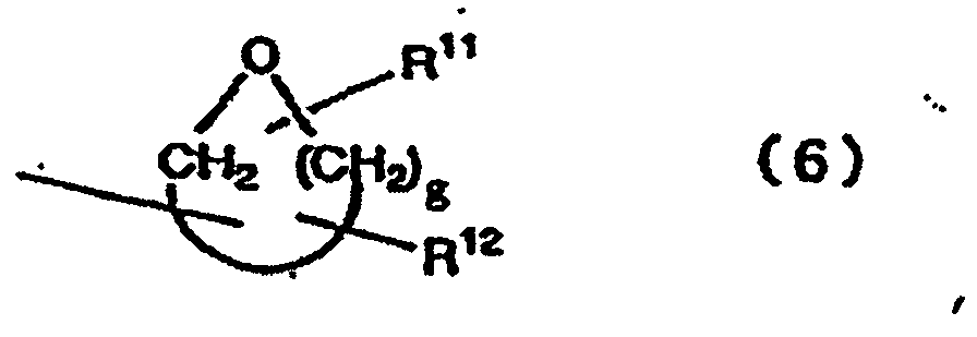
- R 11 and R 12 are each hydrogen atom; an alkyl group, e.g., methyl, ethyl, propyl or butyl, which may have a substituent; aralkyl group, e.g., benzyl or phenethyl, which may have a substituent; or aryl group, e.g., phenyl or naphthyl, which may have a substituent; and g is an integer of 1 to 10.
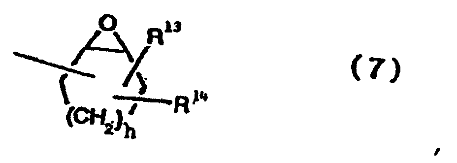
- R 13 and R 14 are each hydrogen atom; an alkyl group, e.g., methyl, ethyl, propyl or butyl, which may have a substituent; aralkyl group, e.g., benzyl or phenethyl, which may have a substituent; or aryl group, e.g., phenyl or naphthyl, which may have a substituent; and h is an integer of 0 to 10.
- R 11 , R 12 , R 13 and R 14 in the general formula (6) or (7) may have include a halogen atom, e.g., fluorine, chlorine, bromine and iodine; alkyl group, e.g., methyl, ethyl, propyl and butyl; alkoxy group, e.g., methoxy, ethoxy and propoxy; aryloxy group, e.g., phenoxy and naphthoxy; aralkyl group, e.g., benzyl, phenethyl, naphthylmethyl, furfuryl and thienyl; and aryl group, e.g., phenyl, naphthyl, anthryl and pyrenyl.
- a halogen atom e.g., fluorine, chlorine, bromine and iodine
- alkyl group e.g., methyl, ethyl, propy
- acryloyloxy group shown by the general formula (8) and methacryloyloxy group shown by the general formula (9) are still more preferable, because of their polymerization-related characteristics, among others.
- the "hole-transporting compound with two or more chain-polymerizing functional groups in the same molecule" for the present invention is the compound in which at least two chain-polymerizing groups described above are bound as the functional groups to a hole-transporting compound through chemical bonds, where "two or more chain-polymerizing functional groups" may be the same or different.
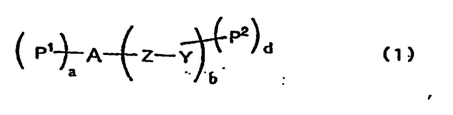
- the hole-transporting compounds with two or more chain-polymerizing functional groups are preferably those shown by the following general formula (1): wherein, P 1 and P 2 are each a chain-polymerizing functional group, and may be the same or different; Z is an organic residue which may have a substituent; Y is hydrogen atom; and a, b and d are each an integer of 0 or more, where b + d is an integer of 3 or more when a is zero, a is an integer of 2 or more when b or d is zero, and a + b + d is an integer of 3 or more in all other cases; P 1 may be the same or different when a is 2 or more, P 2 may be the same or different when d is 2 or more, and Z may be the same or different when b is 2 or more.
- P 1 and P 2 are each a chain-polymerizing functional group, and may be the same or different
- Z is an organic residue which may have a substituent
- Y is hydrogen atom
- the sentence "P 1 may be the same or different when a is 2 or more” means that, when different P 1 of n kinds are represented by P 11 , P 12 , P 13 , P 14 , P 15 ... P 1n and a is 3, the three chain-polymerizing functional groups P 1 directly bound to a hole-transporting compound A may be the same, two may be the same and the other different (e.g., P 11 , P 11 and P 12 ), or all of the three groups may be different from each other (e.g. , P 12 , P 15 and P 17 ).
- the sentences "P 2 may be the same or different when d is 2 or more," and "Z may be the same or different when b is 2 or more” should be read in a similar manner.
- a in the general formula (1) represents a hole-transporting group, and is not limited so long as it shows hole-transporting capacity.
- the hole-transporting groups useful for the present invention include an oxazole derivative, oxadiazole derivative, imidazole derivative, triarylamine derivative, e.g., triphenylamine, 9-(p-diethylaminostyryl)anthracene, 1,1-bis-(4-dibenzylaminophenyl)propane, styrylanthracene, styrylpyrazoline, phenylhydrazones, thiazole derivative, triazole derivative, phenazine derivative, acridine derivative, benzofuran derivative, benzimidazole derivative, thiophene derivative, and N-phenylcarbazole derivative.
- R 4 , R 5 and R 6 are each an alkyl group having a carbon number of 1 to 10, e.g., methyl, ethyl, propyl or butyl, which may have a substituent; aralkyl group, e.g., benzyl, phenethyl, naphthylmethyl, furfuryl or thienyl, which may have a substituent; or aryl group, e.g., phenyl, naphthyl, anthryl, phenanthryl, pyrenyl, thiophenyl, furyl, pyridyl, quinolyl, benzoquinolyl, carbazolyl, phenothiazinyl, benzofuryl, benzothiophenyl, dibenzofuryl or dibenzothiophenyl, which may have a substituent.
- R 4 , R 5 and R 6 are each an alkyl group having a carbon number of 1 to 10, e
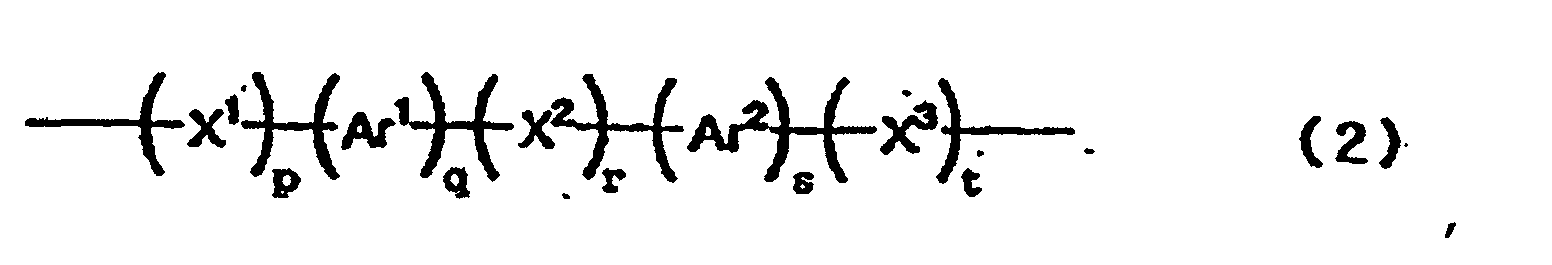
- the ones shown by the following general formula (2) are preferable, and those shown by the general formula (3) are more preferable.
- Ar 1 and Ar 2 are each a divalent arylene group which may have a substituent (the group formed by taking two hydrogen atoms from phenylene, naphthalene, anthracene, phenanthrene, pyrene, benzothiophene, pyridine, quinoline, benzoquinoline, carbazole, phenothiazine, benzofuran, benzothiophene, dibenzofuran, dibenzothiophene, or the like).
- a substituent the group formed by taking two hydrogen atoms from phenylene, naphthalene, anthracene, phenanthrene, pyrene, benzothiophene, pyridine, quinoline, benzoquinoline, carbazole, phenothiazine, benzofuran, benzothiophene, dibenzofuran, dibenzothiophene, or the like).
- R 1 and R 2 are each an alkyl group, e.g., methyl, ethyl or propyl, which may have a substituent; aryl group, e.g., phenyl, naphthyl or thiophenyl, which may have a substituent; or hydrogen atom, where R 1 and R 2 may be the same or different.
- n is an integer of 1 to 5
- p to t are each an integer of 0 to 10, where p to t are not simultaneously zero.
- a substituent the group formed by taking two hydrogen atoms from phenylene, naphthalene, anthracene, phenanthrene, pyrene, benzothiophene, pyridine, quinoline, benzoquinoline, carbazole, phenothiazine, benzofuran, benzothiophene, dibenz
- R 3 is an alkyl group, e.g., methyl, ethyl or propyl, which may have a substituent; aryl group, e.g., phenyl, naphthyl or thiophenyl, which may have a substituent; or hydrogen atom; m' is an integer of 1 to 10; n' is an integer of 1 to 5; and u to w are each an integer of 0 to 10 (where u to w are each particularly preferably an integer of 0 to 5), where u to w are not simultaneously zero.
- R 1 to R 6 , Ar 1 to Ar 3 , X 1 to X 5 and Z in the general formulae (1) to (4) may have include a halogen atom, e.g., fluorine, chlorine, bromine and iodine; nitro group; cyano group; hydroxy group; alkyl group, e.g., methyl, ethyl, propyl and butyl; alkoxy group, e.g., methoxy, ethoxy and propoxy; aryloxy group, e.g., phenoxy and naphthoxy; aralkyl group, e.g., benzyl, phenethyl, naphthylmethyl, furfuryl and thienyl; and aryl group, e.g., phenyl, naphthyl, anthryl and pyrenyl; substituted amino group, e.g., dimethylamino, diethylamino, di
- the hole-transporting compound, useful for the present invention, with two or more chain-polymerizing functional groups in the same molecule preferably has an oxidation potential of 1.2 V or less, more preferably 0.4 to 1.2 V.
- Oxidation potential can be determined by the following procedure:
- Oxidation potential of the hole-transporting compound was determined by an analyzer with a saturated calomel reference electrode and 0.1N (n-Bu) 4 N + ClO 4 - acetonitrile solution as the electrolytic solution, where the potential applied to the working electrodes of platinum was swept by a potential sweeper, to determine the oxidation potential from the peak in the current-potential curve.
- the sample was dissolved in the 0.1N (n-Bu) 4 N + ClO 4 - acetonitrile solution to have a concentration of approximately 5 to 10 mmol%.
- a voltage was applied to the sample solution by the working electrodes in a range from 0 to 1.5 V, in which it was increased linearly to establish the current-potential curve.
- the potential which gave the peak current was defined as the oxidation potential.
- the compound No. 6 was synthesized by the following route:
- the compound No. 71 (3.0 g), prepared by Synthesis Example 2, was dissolved in 20 mL of dichloromethane, cooled to 0 to 5°C, to which 5.2 g of m-chloroperoxybenzoic acid (approximately 70%) was added slowly, stirred for 1 hour, and returned back to room temperature, at which it was stirred for 12 hours.
- the effluent solution was thrown into water, extracted with dichloromethane, and treated to remove the solvent, after the organic layer was dried by anhydrous sodium sulfate.
- the residue was column-purified with silica gel to form 2.1 g of the target compound (the compound No. 55) (oxidation potential: 0.81 V).
- the compound No. 31 was synthesized by the following route:
- Dimethylformamide (DMF, 242.3 g) was cooled to 0 to 5°C, to which 84.8 g of phosphorus oxychloride was slowly added dropwise in such a way to keep the reaction system at 10°C or less.
- the effluent solution was stirred at the same temperature for 15 min, to which a solution of 8 (24 g or 0.093 mol) and DMF (135 g) was slowly added dropwise.
- the effluent was stirred at the same temperature for 30 min, returned back to room temperature at which it was stirred for 2 hours, and heated to 80 to 85°C at which it was stirred for 6 hours.
- Lithium aluminum hydride (1.85 g) was added to 100 mL of dried THF, to which a solution of 9 (15 g or 0.048 mol) and dried THF (100 mL) was slowly added, with stirring at room temperature. On completion of the addition, the effluent was stirred at room temperature for 4 hours, to which 400 mL of an aqueous solution of 5% hydrochloric acid was slowly added dropwise. On completion of the addition, the effluent was extracted with toluene, and the organic layer was dried by anhydrous sodium sulfate to remove the solution. The residue was column-purified with silica gel to form 13 g of 10 .
- the hole-transporting compound is included in a three-dimensional, cross-linked structure at two or more cross-linked points via the covalent bonds in the photosensitive layer by polymerizing/cross-linking the hole-transporting compound with at least two chain-polymerizing functional groups in the same molecule. It is possible to polymerize/cross-link the hole-transporting compound by itself, or after mixing it with another compound with chain-polymerizing group, its type and quantity being not limited.
- the other compound above with chain-polymerizing group may be a monomer, oligomer or polymer with chain-polymerizing group.
- the functional group in the hole-transporting compound is the same as, or polymerizable with, that in the other chain-polymerizing compound, they can be bonded to each other via a covalent bond, to form a three-dimensional, cross-linked, copolymerized structure.
- the photosensitive layer is composed of a mixture of two or more three-dimensional hardened compounds, or of the three-dimensional, hardened compound as the major ingredient which contains the other chain-polymerizing compound monomer or hardened compound thereof. In such a case, it is possible to form an inter penetrating network (IPN) by carefully controlling its compounding ratio and film-making process.
- IPN inter penetrating network
- the photosensitive layer may be made of a monomer, oligomer or polymer which has no group chain-polymerizable with the hole-transporting compound, or of a monomer, oligomer or polymer which has a polymerizable group other than chain-polymerizable one. It is also possible, depending on situations, for the photosensitive layer to contain a hole-transporting compound which is not chemically included into the three-dimensional, cross-linked structure, i.e., a compound having no chain-polymerizing functional group. Moreover, it may be incorporated with other types of additives, e.g., lubricant of finely powdered resin containing fluorine.
- the photosensitive member of the present invention has a photosensitive layer comprising a charge-generating layer containing a charge-generating compound and charge-transporting layer containing a charge-transporting compound, formed one on another on a support in this or reversed order.
- the photosensitive layer may be of a single layer with a charge-generating and charge-transporting compound dispersed therein. In the former laminated type photosensitive layer, two or more charge-transporting layers may be used. In the latter, single-layer photosensitive layer, the layer containing a charge-generating and charge-transporting compound may be further laminated with a charge-transporting layer or protective layer.
- any configuration can be used, so long as the hole-transporting compound with chain-polymerizing groups and/or that compound after being polymerized/cross-linked are included in the photosensitive layer.
- the function-separated type photosensitive member configuration with a charge-generating and charge-transporting layer laminated in this order on a support, is preferable viewed from characteristics of the member, in particular electric characteristics (e.g., residual potential) and durability.
- characteristics of the member in particular electric characteristics (e.g., residual potential) and durability.
- One of the advantages brought by the present invention is durability of the surface layer improved without sacrificing charge-transporting capacity.
- Any material may be used for the support for the electrophotographic photosensitive member of the present invention, so long as it is electroconductive. It may be of a metal, e.g., aluminum, copper, chromium, nickel, zinc or stainless steel, or an alloy, formed into a drum or sheet. It may be also of a plastic film laminated with metallic foil (e.g., aluminum or copper foil) or deposited with aluminum, indium oxide, tin oxide or the like, or metallic film, plastic film or paper provided with an electroconductive layer formed by spreading an electroconductive material by itself or combined with a binder resin.
- a metal e.g., aluminum, copper, chromium, nickel, zinc or stainless steel, or an alloy, formed into a drum or sheet. It may be also of a plastic film laminated with metallic foil (e.g., aluminum or copper foil) or deposited with aluminum, indium oxide, tin oxide or the like, or metallic film, plastic film or paper provided with an electroconductive layer formed by spreading an electroconductive material by itself or combined with
- the present invention may have a subbing layer with barrier and adhesion functions between the support and photosensitive layer.
- the subbing layer is provided for, e.g., improvement of the photosensitive layer in adhesion or paintability, protection of the support, coating defects in the support, improvement in characteristics of injecting charge from the support, or protection of the photosensitive layer from electrical breakdown.
- the materials suitable for the subbing layer include polyvinyl alcohol, poly-N-vinyl imidazole, polyethylene oxide, ethyl cellulose, ethylene-acrylate copolymer, casein, polyamide, N-methoxy-methylated 6-nylon, copolymerized nylon, glue, and gelatin.
- a suitable material dissolved in an adequate solvent is spread over the support and dried. Its thickness is preferably 0.1 to 2 ⁇ m.
- the laminated type photosensitive layer has a charge-generating and charge-transporting layer.
- the materials suitable for the charge-generating layer include dyes based on selenium-tellurium, pyrilium and thiapyrilium, and a variety of central metals and crystalline systems. More concretely, they include crystalline phthalocyanine compounds of ⁇ , ⁇ , y, ⁇ , or X type; pigments of anthoanthorone, dibenzpyrenequinone, pyranthrone, trisazo, dis-azo, monoazo, indigo, quinacridon, asymmetric quinocyanine; quinocyanine; and amorphous silicon (disclosed by Japanese Patent Application Laid-Open No. 54-143645).
- the charge-generating layer is formed by the following procedure: a mixture of the charge-generating material and a 0.3 to 4 times larger quantity of a binder resin is dispersed in a solvent thoroughly by a homogenizer, supersonic disperser, ball mill, vibration ball mill, sand mill, attriter, roll mill or the like, and spread and dried. It is a film of single composition of the charge-generating material, deposited by, e.g., evaporation. Its thickness is preferably 5 ⁇ m or less, more preferably 0.1 to 2 ⁇ m.
- the binder resins useful for the present invention include polymers/copolymers of vinyl compounds, e.g., styrene, vinyl acetate, vinyl chloride, acrylate ester, methacrylate ester, vinylidene fluoride, trifluoroethylene; and polyvinyl alcohol, polyvinyl acetal, polycarbonate, polyester, polysulfone, polyphenylene oxide, polyurethane, cellulosic resin, phenolic resin, melamine resin, silicon-containing resin and epoxy resin.
- vinyl compounds e.g., styrene, vinyl acetate, vinyl chloride, acrylate ester, methacrylate ester, vinylidene fluoride, trifluoroethylene
- polyvinyl alcohol, polyvinyl acetal, polycarbonate, polyester, polysulfone, polyphenylene oxide, polyurethane, cellulosic resin, phenolic resin, melamine resin, silicon-containing resin and epoxy resin e.g.
- the hole-transporting compound with chain-polymerizing functional groups useful for the present invention, can be used for forming the charge-transporting layer on the charge-generating layer, or the surface protective layer having hole-transporting capacity on the charge-transporting layer of the charge-transporting material and binder resin on the charge-generating layer.
- the protective layer, having hole-transporting capacity is within the definition of photosensitive layer.
- a solution containing the hole-transporting compound is spread and then polymerized/cross-linked. It is also possible to form the protective layer using a solution containing the hole-transporting compound, reaction-hardened and then dispersed or dissolved again in a solvent.
- the hole-transporting compound with chain-polymerizing groups for the charge-transporting layer is used at 20 wt.% or more as the hydride adduct of the hole-transporting group (e.g., A in the general formula (1)) based on the whole charge-transporting layer after it is hardened, preferably 40 wt.% or more. At below 20 wt.%, its charge-transporting capacity tends to decrease, possibly causing problems, e.g., decreased sensitivity and increased residual potential. Thickness of the charge-transporting layer is preferably 1 to 50 ⁇ m, more preferably 3 to 30 ⁇ m.
- the charge-transporting layer below the protective layer can be formed by coating and drying a solution of an adequate charge-transporting compound and binder resin (which can be selected from the above resins for the charge-generating layer) dispersed/dissolved in a solvent.
- an adequate charge-transporting compound and binder resin which can be selected from the above resins for the charge-generating layer
- the adequate charge-transporting compounds include polymers having heterocyclic or condensed polycyclic aromatic compounds, e.g., poly-N-vinylcarbazole and polystyryl anthracene; heterocyclic compounds, e.g., pyrazoline, imidazole, oxazole, triazole and carbazole; triaryl alkane derivatives, e.g., triphenylmethane; triarylamine derivatives, e.g., triphenylamine; and low-molecular-weight compounds, e.g., phenylenediamine derivatives, N-phenylcarbazole derivatives, stilbene derivatives and hydrazine derivatives.
- heterocyclic compounds e.g., pyrazoline, imidazole, oxazole, triazole and carbazole
- triaryl alkane derivatives e.g., triphenylmethane
- triarylamine derivatives e.g., trip
- the charge-transporting compound accounts for preferably 30 to 100% by weight based on 100% of the total composition of the charge-transporting compound and binder resin, more preferably 50 to 100% by weight At below 30% by weight of the charge-transporting compound, charge-transporting capacity may decrease, possibly causing problems such as decreased sensitivity and increased residual potential.
- Thickness of the charge-transporting layer is preferably 1 to 50 ⁇ m as total thickness of the upper surface-protective layer and charge-transporting layer, more preferably 5 to 30 ⁇ m.
- the photosensitive layer containing the hardened hole-transporting compound with chain-polymerizing groups may be incorporated with the charge-transporting compound.
- the photosensitive layer may be formed by polymerizing/cross-linking a solution containing both hole-transporting and charge-generating compounds, or the single-layered photosensitive layer containing both hole-transporting and charge-generating compounds may be coated with a solution containing the hole-transporting compound to be polymerized/cross-linked thereon.
- the photosensitive layer for the present invention may be incorporated with various additives, including an inhibitor (e.g., antioxidant agent or ultraviolet ray absorber), or a lubricant (e.g., finely powdered resin containing fluorine).
- an inhibitor e.g., antioxidant agent or ultraviolet ray absorber
- a lubricant e.g., finely powdered resin containing fluorine
- the methods for spreading a solution to form each layer include dip coating, spray coating, curtain coating and spin coating. Of these, dip coating is more preferable than the others, because of its high efficiency/productivity.
- the known film-making processes, e.g., evaporation and plasma-aided one, may be adequately selected for the present invention.
- the hole-transporting compound with chain-polymerizing groups useful for the present invention, is polymerized/cross-linked by the aid of electron ray.
- the electron ray is used because it can dispense with a polymerization initiator, which is one of the most notable advantages of this process. This will make it possible to form a three-dimensional photosensitive matrix of very high purity, and secure good electrophotographic characteristics. Its productivity is also high, because polymerization is effected more efficiently in a shorter time. Another advantage comes from high permeability of electron ray, which hardens the layer while being much less affected by a shielding material, e.g., an additive or the like, present in the layer or forming a thick layer.
- a shielding material e.g., an additive or the like
- the polymerization may be retarded, depending on type of the chain-polymerizing group used or type of its central skeleton.
- a polymerization initiator may be additionally used in an acceptable range.
- the ray used in the present invention is electron ray because of its capacity to enhance polymerization efficiency.
- Suitable accelerators for electron ray include scanning, electrocurtain, broad beam, pulse and laminar types. It is very important to set adequate irradiation conditions, since the electron ray is used, for the photosensitive layer to manifest the electrical characteristics and durability.
- the hole-transporting compound is irradiated with electron ray, accelerated preferably at 300 KV or less, more preferably 150 KV or less, at an irradiation dose preferably in a range from 1 to 100 Mrad, more preferably from 3 to 50 Mrad. Deterioration of the photosensitive characteristics increases as acceleration voltage of the electron ray increases beyond 300 KV. For irradiation dose, cross-linking will be insufficient at below 1 Mrad, and the photosensitive characteristics tend to be deteriorated at above 100 Mrad.
- FIGURE illustrates the electrophotographic apparatus equipped with the process cartridge having the electrophotographic photosensitive member of the present invention.
- the drum-shaped electrophotographic photosensitive member 1 of the present invention is driven to rotate around the axis 2 at a given circumferential speed in the arrowed direction.
- the member 1 is uniformly electrified positively or negatively at a given potential by the primary electrifying means 3, while being rotated, and then exposed to light 4 by an exposure means, e.g., slit or laser beam scanning (not shown).
- an exposure means e.g., slit or laser beam scanning (not shown).
- the electrostatic latent image formed is then developed with a toner by the developing means 5, and the developed image is transferred one after another by the transferring means 6 to the transfer paper 7, which is supplied syncr 'nously with rotation of the photosensitive member 1 from a paper feeder (not shown) to the space between the photosensitive member 1 and transferring means 6.
- the transfer paper 7, on receiving the developed image, is separated from the photosensitive member 1 and sent to the image fixing means 8, where the image is fixed.
- the fixed image is printed out as a copy by a printer outside of this electrophotographic apparatus.
- the surface of the photosensitive member 1 is cleaned by the cleaning means 9 to remove the residual toner, after the image is transferred, and treated by front exposure light 10 emitted from an exposure means (not shown) to remove electricity, for repeated use for forming images.
- front exposure light may be dispensed with.
- some of the constitutional members e.g., the electrophotographic photosensitive member 1, primary electrifying means 3, developing means 5 and cleaning means 9, can be integrated into a process cartridge assembly, which is freely attached to or detached from an electrophotographic apparatus body, e.g., a copier or laser beam printer.
- a process cartridge assembly which is freely attached to or detached from an electrophotographic apparatus body, e.g., a copier or laser beam printer.
- at least one of the primary electrifying means 3, developing means 5 and cleaning means 9 is supported together with the photosensitive member 1 to form a cartridge assembly, e.g., the process cartridge 11 attachable to or detachable from the apparatus body using a guiding means, e.g., rail 12 in the apparatus body.
- the exposure light 4 is the light reflected from or passing through an original image, or the laser beam scanned in accordance with a signal of the original image read by a sensor and signalized, or the light irradiated by driving an LED array or liquid-crystalline shutter array.
- the electrophotographic photosensitive member of the present invention can be widely used in electrophotographic application devices, e.g., laser beam printers, CRT printers, LED printers, liquid-crystalline printers and laser-aided printers, not limited to electrophotographic copiers.
- electrophotographic application devices e.g., laser beam printers, CRT printers, LED printers, liquid-crystalline printers and laser-aided printers, not limited to electrophotographic copiers.
- the coating material for the electroconductive layer was prepared by the following procedure. A mixture of 50 parts of electroconductive titanium oxide particles coated with tin oxide containing antimony oxide at 10%, 25 parts of phenolic resin, 20 parts of methylcellsolve, 5 parts of methanol and 0.002 parts of silicone oil (polydimethyl siloxane/polyoxyalkylene copolymer having an average molecular weight of 3,000) was prepared by dispersing these components by a sand mill with glass beads (diameter: 1 mm) for 2 h. This coating material was spread by dip coating over an aluminum cylinder (diameter: 30 mm) and dried at 140°C for 30 min, to form a 20 ⁇ m thick electroconductive layer on the cylinder.
- silicone oil polydimethyl siloxane/polyoxyalkylene copolymer having an average molecular weight of 3,000
- the coating material for the intermediate layer was prepared by dissolving 5 parts of N-methoxymethylated nylon in 95 parts of methanol. This coating material was spread by dip coating over the above electroconductive layer and dried at 100°C for 20 min, to form a 0.6 ⁇ m thick intermediate layer thereon.
- a mixture of 5 parts of a bis-azo pigment shown by the following structural formula A, 2 parts of polyvinyl butylal resin and 60 parts of cyclohexanone was prepared by dispersing these components by a sand mill with glass beads (diameter: 1 mm) for 24 h, to which 60 parts of tetrahydrofuran was added to prepare the coating material for the charge-generating layer.
- This coating material was spread by dip coating over the intermediate layer and dried at 100°C for 15 min, to form a 0.2 ⁇ m thick charge-generating layer.
- the compound No. 6 as the hole-transporting compound (60 parts) was dissolved in a mixed solvent of monochlorobenzene (30 parts) and dichloromethane (30 parts), to prepare the coating material for the charge-transporting layer.
- This coating material was spread over the charge-generating layer, and irradiated with electron ray under the conditions of accelerating voltage: 150 KV and irradiation dose: 30 Mrad, and hardened to form a 15 ⁇ m thick charge-transporting layer, completing the electrophotographic photosensitive member.
- the electrophotographic photosensitive member thus prepared was assessed for its temporal separation , electrophotographic characteristics and durability.
- the temporal separation was assessed by an acceleration test in which the sample was preserved at 75°C for 14 days with a cleaning blade of urethane rubber for copiers pressed to the sample surface. It was then microscopically observed to judge whether there was a separation or not. When there was no separation observed, the test was further continued for a total of 30 days.
- the electrophotographic characteristics and durability were assessed by setting up the sample in a copier (Canon Inc., LBP-SX).
- the initial photosensitive member characteristics [potential at the dark section Vd, light decay sensitivity (quantity of light necessary to decay potential at the dark section set at -700 V to -150 V), and residual potential Vsl (potential when the sample was irradiated with light 3 times as large a quantity as that for light decay sensitivity)] were measured.
- the durability test in which an original image was copied 10,000 times was conducted, to observe whether there was a defective copy or not visually, wear of the photosensitive member, and the photosensitive member characteristics, and to determine changes in the characteristics, ⁇ Vd, ⁇ Vl (difference between quantity of light necessary to set the initial Vl at -150 V and Vl of the durability-tested sample irradiated with the same quantity of light) and ⁇ Vsl.
- the results are given in Table 1.
- the photosensitive member showed very stable and good characteristics: no separation was observed on the tested photosensitive member, its photosensitive characteristics were good, only a limited extent of wear was observed, and photosensitive characteristics changed little by the durability test.
- Example Hole-transporting Compound No. Example Hole-transporting Compound No. 2 27 14 25 3 29 15 101 4 31 16 114 5 32 17 55 6 113 18 56 7 11 19 112 8 13 20 111 9 7 21 71 10 4 22 116 11 5 23 117 12 23 24 118 13 24 25 119
- Example 1 The same procedure as used for Example 1 was repeated, except that 48 parts of the compound No. 6 as the hole-transporting compound was used and 12 parts of an acrylic monomer shown by the structural formula (B) was added, to prepare and assess the electrophotographic photosensitive member. The results are given in Table 1.
- Example 7 The same procedure as used for Example 7 was repeated, except that 48 parts of the compound No. 11 as the hole-transporting compound was used and 12 parts of an acrylic monomer shown by the structural formula (C) was added, to prepare and assess the electrophotographic photosensitive member.
- the results are given in Table 1.
- Example 1 The same procedure as used for Example 1 was repeated, except that 48 parts of the compound No. 6 as the hole-transporting compound was used and 12 parts of the acrylic oligomer (number-average molecular weight: 2,000) shown by the structural formula (D) was added, to prepare and assess the electrophotographic photosensitive member.
- the results are given in Table 1.
- Example Irradiation condition (accelerqation volt/ray dose) 29 200Kv/30Mrad 30 300/30 31 150/80 32 150/150 33 150/200
- Example 1 The same procedure as used for Example 1 was repeated to form the charge-generation layer.
- the compound No. 6 as the hole-transporting compound (60 parts) was dissolved in a mixed solvent of monochlorobenzene (50 parts) and dichloromethane (50 parts), to prepare the coating material for the surface protective layer.
- This coating material was spread over the charge-transporting layer by spray coating, and irradiated with electron ray under the conditions of accelerating voltage: 150 KV and irradiation dose: 30 Mrad, and hardened to form a 5 ⁇ m thick surface protective layer, completing the electrophotographic photosensitive member.
- the same procedure as used for Example 1 was used to assess the electrophotographic photosensitive member. The results are given in Table 2.
- Example 34 The same procedure as used for Example 34 was repeated, except that the compound No. 6 as the hole-transporting compound was replaced by the compound No. 7 as the hole-transporting compound, to prepare and assess the electrophotographic photosensitive member.
- the results are given in Table 2.
- Example 34 The same procedure as used for Example 34 was repeated, except that 30 parts of the compound No. 6 as the hole-transporting compound was used and 30 parts of the acrylic monomer shown by the structural formula (B), used for Example 26, was added, to prepare and assess the electrophotographic photosensitive member.
- the results are given in Table 2.
- Example 34 The same procedure as used for Example 34 was repeated, except that 30 parts of the compound No. 6 as the hole-transporting compound was used and 30 parts of the acrylic oligomer shown by the structural formula (D), used for Example 28, was added, to prepare and assess the electrophotographic photosensitive member.
- the results are given in Table 2.
- Example 2 The same procedure as used for Example 1 was repeated to form the charge-generation layer.
- the compound No. 6 as the hole-transporting compound (60 parts) and 0.6 parts of a photopolymerization initiator shown by the structural formula (J) were dissolved in a mixed solvent of monochlorobenzene (30 parts) and dichloromethane (30 parts), to prepare the coating material for the charge-transporting layer.
- This coating material was spread over the charge-generating layer, and irradiated with light emitted from a metal halide lamp at an intensity of 500 mW/cm 2 for 30 sec, and hardened to form a 15 ⁇ m thick charge-transporting layer, completing the electrophotographic photosensitive member.
- the same procedure as used for Example 1 was used to assess the electrophotographic photosensitive member.
- the results are given in Table 3.
- the photosensitive member showed very stable and good characteristics: no separation was observed on the tested photosensitive member, its photosensitive characteristics were good, only a limited extent of wear was observed, and photosensitive characteristics changed little by the durability test
- Example 38 The same procedure as used for Example 38 was repeated for each of Examples 39 to 48, except that the compound No. 6 as the hole-transporting compound was replaced by the one shown in the following table, to prepare and assess the electrophotographic photosensitive members. The results are given in Table 2.
- Example Hole-transporting Compound No. Example Hole-transporting Compound No. 39 31 45 5 40 113 46 101 41 11 47 114 42 13 48 116 43 7 49 55 44 4 50 56 51 111
- Example 38 The same procedure as used for Example 38 was repeated, except that the compound No. 6 as the hole-transporting compound was replaced by the compound No. 117, and 0.3 parts of the photopolymerization initiator (J) and 0.3 parts of the photopolymerization initiator (K) were added, to prepare and assess the electrophotographic photosensitive member.
- the results are given in Table 2.
- Example 38 The same procedure as used for Example 38 was repeated, except that the photopolymerization initiator (J) was replaced by a thermal polymerization initiator shown by the structural formula (L): and hardening by the aid of ultraviolet ray was replaced by hardening under heating at 140°C for 1 h, to prepare and assess the electrophotographic photosensitive member.
- the results are given in Table 2.
- Example 53 The same procedure as used for Example 53 was repeated, except that the compound No. 6 as the hole-transporting compound was replaced by the compound No. 71, to prepare and assess the electrophotographic photosensitive member.
- the results are given in Table 2.
- Example 53 The same procedure as used for Example 53 was repeated, except that the compound No. 6 as the hole-transporting compound was replaced by the compound No. 112, to prepare and assess the electrophotographic photosensitive member.
- the results are given in Table 2.
- Example 38 The same procedure as used for Example 38 was repeated, except that 48 parts of the compound No. 6 as the hole-transporting compound was used and 12 parts of the acrylic monomer shown by the structural formula (B) was added, to prepare and assess the electrophotographic photosensitive member.
- the results are given in Table 2.
- Example 49 The same procedure as used for Example 49 was repeated, except that 48 parts of the compound No. 55 as the hole-transporting compound was used and 12 parts of an epoxy monomer shown by the structural formula (M) was added, to prepare and assess the electrophotographic photosensitive member.
- the results are given in Table 2.
- Example 38 The same procedure as used for Example 38 was repeated, except that 48 parts of the compound No. 6 as the hole-transporting compound was used and 12 parts of the acrylic oligomer (number-average molecular weight: 2,000) shown by the structural formula (D) was added, to prepare and assess the electrophotographic photosensitive member.
- the results are given in Table 2.
- Example 53 The same procedure as used for Example 53 was repeated, except that 48 parts of the compound No. 6 as the hole-transporting compound was used and 12 parts of the acrylic monomer shown by the structural formula (B) was added, to prepare and assess the electrophotographic photosensitive member.
- the results are given in Table 2.
- Example 34 The same procedure as used for Example 34 was repeated to form the charge-transporting layer.
- the compound No. 6 as the hole-transporting compound (60 parts) and 0.6 parts of a photopolymerization initiator shown by the structural formula (J) were dissolved in a mixed solvent of monochlorobenzene (50 parts) and dichloromethane (50 parts), to prepare the coating material for the surface protective layer.
- This coating material was spread over the charge-transporting layer by spray coating, and irradiated with light emitted from a metal halide lamp at an intensity of 500 mW/cm 2 for 30 sec, and hardened to form a 5 ⁇ m thick surface of protective layer, completing the electrophotographic photosensitive member.
- the same procedure as used for Example 38 was used to assess the electrophotographic photosensitive member. The results are given in Table 2.
- Example 60 The same procedure as used for Example 60 was repeated, except that the compound No. 6 as the hole-transporting compound was replaced by the compound No. 55 as the hole-transporting compound, and the photopolymerization initiator shown by the structural formula (J) was replaced by the photopolymerization initiator shown by the structural formula (K), to prepare and assess the electrophotographic photosensitive member.
- the results are given in Table 2.
- Example 60 The same procedure as used for Example 60 was repeated, except that 30 parts of the compound No. 6 as the hole-transporting compound was used and 30 parts of the acrylic monomer shown by the structural formula (B) was added, to prepare and assess the electrophotographic photosensitive member.
- the results are given in Table 2.
- Example 61 The same procedure as used for Example 61 was repeated, except that 30 parts of the compound No. 55 as the hole-transporting compound was used and 30 parts of the epoxy monomer shown by the structural formula (M) was added, to prepare and assess the electrophotographic photosensitive member.
- the results are given in Table 2.
- Example 62 The same procedure as used for Example 62 was repeated, except that the acrylic monomer shown by the structural formula (B) was replaced by the acrylic oligomer (number-average molecular weight: 2,000) shown by the structural formula (D), to prepare and assess the electrophotographic photosensitive member.
- the results are given in Table 2.
- Example 1 The same procedure as used for Example 1 was repeated to form the charge-generation layer.
- the styryl compound shown by the structural formula (E) (15 parts) and 15 parts of polymethyl methacrylate resin (number-average molecular weight: 40,000) having a repeating unit shown by the structural formula (G) were dissolved in a mixed solvent of monochlorobenzene (50 parts) and dichloromethane (20 parts), to prepare the coating material for the charge-transporting layer. This coating material was spread over the charge-generating layer, to form the 15 ⁇ m thick of charge-transporting layer, completing the electrophotographic photosensitive member.
- Example 1 The same procedure as used for Example 1 was used to assess the electrophotographic photosensitive member. A separation was observed in 14 days. Although it showed good initial electrophotographic characteristics, but was worn more in the surface layer, when durability-tested, showing defective images, e.g., fogging and scratches. The charge-transporting layer was worn to lose its thickness, after 8,000 copies were produced, causing failure of electrification and no longer possible to produce the copies. The results are given in Table 3.
- Example 34 The same procedure as used for Example 34 was repeated to form the charge-transporting layer.
- Example 34 The same procedure as used for Example 34 was used to assess the electrophotographic photosensitive member. It showed neither decrease in sensitivity nor increase in residual potential, because of the presence of the charge-transporting layer of high charge-transporting capacity under the surface protective layer, and produced no ghost images. Nevertheless, however, it was still insufficient in durability, because the images produced during the durability test still suffered scratches and fogging. The results are given in Table 3.
- Example 3 The same procedure as used for Example 1 was repeated, except that the compound No.6 as the hole-transporting compound was replaced by the compound shown by the structural formula (H), disclosed by Japanese Patent Application Laid-Open No. 5-216249, to form and assess the electrophotographic photosensitive member.
- the electrophotographic photosensitive member showed good initial electrophotographic characteristics, but was much less durable than the one prepared by Example 1. The results are given in Table 3.
- Example 26 The same procedure as used for Example 26 was repeated, except that the compound No.6 as the hole-transporting compound was replaced by the compound shown by the structural formula (H), to form and assess the electrophotographic photosensitive member.
- the electrophotographic photosensitive member showed good initial electrophotographic characteristics, but was much less durable than the one prepared by Example 26. The results are given in Table 3.
- Example 1 The same procedure as used for Example 1 was repeated to form the charge-generation layer.
- Example 38 The same procedure as used for Example 38 was repeated, except that the compound No.6 as the hole-transporting compound was replaced by the compound shown by the structural formula (H), to form and assess the electrophotographic photosensitive member.
- the electrophotographic photosensitive member showed good initial electrophotographic characteristics, but was much less durable than the one prepared by Comparative Example 38. The results are given in Table 3.
Claims (18)
- Elektrofotographisches lichtempfindliches Element, das einen Träger und darauf eine lichtempfindliche Schicht umfasst, wobei die lichtempfindliche Schicht eine gehärtete Leerstellen transportierende Verbindung enthält, wobei die Leerstellen transportierende Verbindung vor dem Härten zwei oder mehr kettenpolymerisierende funktionelle Gruppen in dem gleichen Molekül aufweist und die Leerstellen transportierende Verbindung durch Bestrahlung mit einem Elektronenstrahl gehärtet ist.
- Elektrofotographisches lichtempfindliches Element nach Anspruch 1, wobei die Leerstellen transportierende Verbindung durch die allgemeine Formel (1) gezeigt ist:wobei A eine Leerstellen transportierende Gruppe ist, P1 und P2 beide eine kettenpolymerisierende funktionelle Gruppe sind und gleich oder verschieden sein können, Z ein organischer Rest ist, der einen Substituenten haben kann, Y ein Wasserstoffatom ist und a, b und d jeweils eine ganze Zahl von null oder größer sind, wobei b + d eine ganze Zahl von 3 oder größer ist, wenn a null ist, a eine ganze Zahl von 2 oder größer ist, wenn b oder d null ist, und a + b + d eine ganze Zahl von 3 oder größer in allen anderen Fällen ist, und P1 gleich oder verschieden sein kann, wenn a 2 oder größer ist, P2 gleich oder verschieden sein kann, wenn d 2 oder größer ist und Z gleich oder verschieden sein kann, wenn b 2 oder größer ist.
- Elektrofotographisches lichtempfindliches Element nach Anspruch 2, wobei Z in der allgemeinen Formel (1) eine Alkylengruppe, die einen Substituenten haben kann, eine Arylengruppe, die einen Substituenten haben kann, CR1=CR2 (wobei R1 und R2 jeweils eine Alkylgruppe sind, die einen Substituenten haben kann, eine Arylgruppe, die einen Substituenten haben kann, oder ein Wasserstoffatom sind und gleich oder verschieden sein können), C=O, S=O, SO2 oder ein organischer Rest ist, der wenigstens eines von Sauerstoff- und Schwefelatomen enthält, die beliebig miteinander kombiniert sein können.
- Elektrofotographisches lichtempfindliches Element nach Anspruch 3, wobei Z in der allgemeinen Formel (1) durch die folgende allgemeine Formel (2) gezeigt ist:wobei X1 bis X3 jeweils eine Alkylengruppe, die einen Substituenten haben kann, (CR1=CR2)m, C=O, S=O, SO2 oder ein Sauerstoff- oder ein Schwefelatom sind, Ar1 und Ar2 beide eine Arylgruppe sind, die einen Substituenten haben kann,
R1 und R2 beide eine Alkylgruppe, die einen Substituenten haben kann, eine Arylgruppe, die einen Substituenten haben kann, oder ein Wasserstoffatom sind, wobei R1 und R2 gleich oder verschieden sein können, und
m eine ganze Zahl von 1 bis 5 ist und p bis t jeweils eine ganze Zahl von 0 bis 10 sind, wobei p bis t nicht gleichzeitig null sind. - Elektrofotographisches lichtempfindliches Element nach Anspruch 4, wobei Z in der allgemeinen Formel (1) durch die folgende allgemeine Formel (3) gezeigt ist:wobei Ar3 eine Arylengruppe ist, die einen Substituenten haben kann, X4 und X5 jeweils (CH2)m', (CH=CR3)n', C=O oder ein Sauerstoffatom sind,

R3 eine Alkylgruppe, die einen Substituenten haben kann, eine Arylgruppe, die einen Substituenten haben kann, oder ein Wasserstoffatom ist und m eine ganze Zahl von 1 bis 10 ist, n eine ganze Zahl von 1 bis 5 ist und u bis w jeweils eine ganze Zahl von 0 bis 10 sind, wobei u bis w nicht gleichzeitig null sind. - Elektrofotographisches lichtempfindliches Element nach Anspruch 2, wobei jedes von P' und Z in A durch ein Wasserstoffatom substituiert ist, um ein durch die folgende allgemeine Formel (4) gezeigtes Wasserstoffaddukt zu bilden:wobei R4, R5 und R6 jeweils eine Alkylgruppe, die einen Substituenten haben kann, eine Aralkylgruppe, die einen Substituenten haben kann, oder eine Arylgruppe, die einen Substituenten haben kann, sind und R4, R5 und R6 gleich oder verschieden sein können und wenigstens zwei von ihnen Arylgruppen sind.

- Elektrofotographisches lichtempfindliches Element nach Anspruch 6, wobei R4, R5 und R6 alle eine Arylgruppe sind.
- Elektrofotographisches lichtempfindliches Element nach Anspruch 2, wobei wenigstens eines von P1 und P2 eine ungesättigte polymerisierende funktionelle Gruppe ist, die durch die folgende allgemeine Formel (5) gezeigt ist:wobei E ein Wasserstoffatom, ein Halogenatom, eine Alkylgruppe, die einen Substituenten haben kann, eine Aralkylgruppe, die einen Substituenten haben kann, eine Arylgruppe, die einen Substituenten haben kann, eine Cyanogruppe, eine Nitrogruppe, eine Alkoxygruppe, -COOR7 (wobei R7 ein Wasserstoffatom, ein Halogenatom, eine Alkylgruppe, die einen Substituenten haben kann, eine Aralkylgruppe, die einen Substituenten haben kann, oder eine Arylgruppe, die einen Substituenten haben kann, ist), CONR8R9 (wobei R8 und R9 jeweils ein Wasserstoffatom, ein Halogenatom, eine Alkylgruppe, die einen Substituenten haben kann, eine Aralkylgruppe, die einen Substituenten haben kann, oder eine Arylgruppe, die einen Substituenten haben kann, sind, wobei R8 und R9 gleich oder verschieden sein können) und W eine Arylengruppe, die einen Substituenten haben kann, eine Alkylengruppe, die einen Substituenten haben kann, oder -COO-, -CH2-, -O-, -OO- -S- oder CONR10 ist (wobei R10 ein Wasserstoffatom, ein Halogenatom, eine Alkylgruppe, die einen Substituenten haben kann, eine Aralkylgruppe, die einen Substituenten haben kann, oder eine Arylgruppe, die einen Substituenten haben kann, ist) und f 0 oder 1 ist.

- Elektrofotographisches lichtempfindliches Element nach Anspruch 2, wobei wenigstens eines von P1 und P2 eine cyclische Ethergruppe ist, die durch die folgende allgemeine Formel (6) gezeigt ist:wobei R11 und R12 jeweils ein Wasserstoffatom, eine Alkylgruppe, die einen Substituenten haben kann, eine Aralkylgruppe, die einen Substituenten haben kann, oder eine Arylgruppe, die einen Substituenten haben kann, sind und g eine ganze Zahl von 1 bis 10 ist.
- Elektrofotographisches lichtempfindliches Element nach Anspruch 2, wobei wenigstens eines von P1 und P2 eine alicyclische Epoxidgruppe ist, die durch die folgende allgemeine Formel (7) gezeigt ist:wobei R13 und R14 jeweils ein Wasserstoffatom, eine Alkylgruppe, die einen Substituenten haben kann, eine Aralkylgruppe, die einen Substituenten haben kann, oder eine Arylgruppe, die einen Substituenten haben kann, sind und h eine ganze Zahl von 0 bis 10 ist.
- Elektrofotographisches lichtempfindliches Element nach Anspruch 2, wobei wenigstens eines von P1 und P2 durch eine Formel ausgedrückt wird, die aus der Gruppe ausgewählt ist, die aus den Formeln (8) bis (14) besteht:

 wobei i eine ganze Zahl von 1 bis 3 ist, und
 wobei j eine ganze Zahl von 1 bis 3 ist.
- Elektrofotographisches lichtempfindliches Element nach Anspruch 11, wobei wenigstens eins von P1 und P2 durch eine Formel ausgedrückt wird, die aus der Gruppe ausgewählt ist, die aus den Formeln (8) und (9) besteht:

- Verfahrenskartusche, die ein elektrofotographisches lichtempfindliches Element nach Anspruch 1 und wenigstens eine Einrichtung ausgewählt aus der Gruppe bestehend aus jenen zum Elektrifizieren, zur Entwicklung und zum Reinigen umfasst,
wobei das elektrofotographische lichtempfindliche Element und wenigstens eine der Einrichtungen monolithisch getragen werden, um eine Anordnung auszubilden, die frei an den Körper eines elektrofotographischen Geräts angebracht oder davon abgenommen werden kann. - Elektrofotographisches Gerät, das ein elektrofotographisches lichtempfindliches Element nach Anspruch 1 und Einrichtungen zum Elektrifizieren, zur Belichtung, zur Entwicklung und zur Übertragung umfasst.
- Verfahren zur Herstellung eines elektrofotographischen lichtempfindlichen Elements nach einem der Ansprüche 1 bis 12 mit den Schritten:(i) Erzeugung einer Schicht, die eine Leerstellen transportierende Verbindung mit zwei oder mehr kettenpolymerisierenden funktionellen Gruppen in dem gleichen Molekül für das elektrofotographische lichtempfindliche Element umfasst, und(ii) Bestrahlen der in dem Schritt (i) erhaltenen Schicht mit einem Elektronenstrahl, um die Schicht auszuhärten, und Erzeugen der lichtempfindlichen Schicht.
- Verfahren zur Herstellung eines elektrofotographischen lichtempfindlichen Elements nach Anspruch 15, wobei die Polymerisation/das Vernetzen ohne Verwendung eines Polymerisationsstarters durchgeführt wird.
- Verfahren zur Herstellung eines elektrofotographischen lichtempfindlichen Elements nach Anspruch 15, wobei das elektrofotographische lichtempfindliche Element mit einem Elektronenstrahl bei einer Beschleunigungsspannung von 300 kV oder weniger bestrahlt wird.
- Verfahren zur Herstellung eines elektrofotographischen lichtempfindlichen Elements nach Anspruch 15, wobei das elektrofotographische lichtempfindliche Element mit einem Elektronenstrahl bei einer Dosis von 1 bis 100 Mrad bestrahlt wird.
Applications Claiming Priority (4)
| Application Number | Priority Date | Filing Date | Title |
|---|---|---|---|
| JP16493198 | 1998-06-12 | ||
| JP16493198 | 1998-06-12 | ||
| JP16493098 | 1998-06-12 | ||
| JP16493098 | 1998-06-12 |
Publications (2)
| Publication Number | Publication Date |
|---|---|
| EP0964309A1 EP0964309A1 (de) | 1999-12-15 |
| EP0964309B1 true EP0964309B1 (de) | 2005-12-07 |
Family
ID=26489857
Family Applications (1)
| Application Number | Title | Priority Date | Filing Date |
|---|---|---|---|
| EP99111424A Expired - Lifetime EP0964309B1 (de) | 1998-06-12 | 1999-06-11 | Elektrophotographisches, lichtempfindliches Element, Verfahrenskassette und elektrophotographischer Apparat, sowie Verfahren zur Herstellung des lichtempfindlichen Elementes |
Country Status (3)
| Country | Link |
|---|---|
| US (1) | US6180303B1 (de) |
| EP (1) | EP0964309B1 (de) |
| DE (1) | DE69928725T2 (de) |
Families Citing this family (59)
| Publication number | Priority date | Publication date | Assignee | Title |
|---|---|---|---|---|
| DE69927567T2 (de) * | 1998-11-13 | 2006-06-14 | Canon Kk | Elektrophotographisches lichtempfindliches Element, Verfahrenskassette und elektrophotographischer Apparat |
| US6372397B1 (en) * | 1999-01-06 | 2002-04-16 | Canon Kabushiki Kaisha | Electrophotographic photosensitive member, process cartridge and electrophotographic apparatus |
| US6410195B1 (en) * | 1999-08-12 | 2002-06-25 | Canon Kabushiki Kaisha | Electrophotographic photosensitive member, process cartridge, and electrophotographic apparatus |
| US7179573B2 (en) * | 2003-03-20 | 2007-02-20 | Ricoh Company, Ltd. | Electrophotographic photoconductor, and image forming process, image forming apparatus and process cartridge for an image forming apparatus using the same |
| US7175957B2 (en) * | 2003-03-20 | 2007-02-13 | Ricoh Company, Ltd. | Electrophotographic photoconductor, and image forming process, image forming apparatus and process cartridge for an image forming apparatus using the same |
| EP2328029B1 (de) | 2003-07-25 | 2012-05-23 | Canon Kabushiki Kaisha | Elektrophotographisches, lichtempfindliches Element, Prozesskartusche und elektrophotographischer Apparat |
| US6768010B1 (en) * | 2003-09-16 | 2004-07-27 | Samsung Electronics Co., Ltd. | Organophotoreceptor with an epoxy-modified charge transport compound having an azine group |
| WO2005054957A1 (ja) * | 2003-12-01 | 2005-06-16 | Ricoh Company, Ltd. | 電子写真感光体、画像形成方法、画像形成装置、画像形成装置用プロセスカートリッジ |
| JP2005250455A (ja) * | 2004-02-03 | 2005-09-15 | Canon Inc | 電子写真装置 |
| WO2005093520A1 (ja) * | 2004-03-26 | 2005-10-06 | Canon Kabushiki Kaisha | 電子写真感光体、電子写真感光体の製造方法、プロセスカートリッジ および電子写真装置 |
| JP4249681B2 (ja) * | 2004-09-06 | 2009-04-02 | 株式会社リコー | 画像形成装置及びプロセスカートリッジ |
| JP4785366B2 (ja) * | 2004-10-20 | 2011-10-05 | キヤノン株式会社 | 画像形成装置 |
| DE602005011242D1 (de) | 2004-12-24 | 2009-01-08 | Ricoh Kk | Elektrofotografischer Fotorezeptor und Bilderzeugungsverfahren, Bilderzeugungsvorrichtung und Prozesskartusche dafür mit dem elektrofotografischen Fotorezeptor |
| CN101189558B (zh) * | 2005-06-02 | 2010-12-08 | 佳能株式会社 | 电子照相感光构件、处理盒和电子照相设备 |
| JP4194631B2 (ja) * | 2006-01-31 | 2008-12-10 | キヤノン株式会社 | 画像形成方法ならびに該画像形成方法を用いた電子写真装置 |
| JP4101279B2 (ja) * | 2006-01-31 | 2008-06-18 | キヤノン株式会社 | 電子写真感光体、プロセスカートリッジおよび電子写真装置 |
| JP4101278B2 (ja) * | 2006-01-31 | 2008-06-18 | キヤノン株式会社 | 電子写真感光体、プロセスカートリッジおよび電子写真装置 |
| JP4605126B2 (ja) * | 2006-09-11 | 2011-01-05 | コニカミノルタビジネステクノロジーズ株式会社 | 電子写真感光体 |
| US7648810B2 (en) * | 2006-09-14 | 2010-01-19 | Xerox Corporation | Liquid ink resistant photoreceptor |
| JP4771909B2 (ja) | 2006-10-31 | 2011-09-14 | 株式会社リコー | 電子写真感光体、それを用いた画像形成方法、画像形成装置及び画像形成装置用プロセスカートリッジ、及び電子写真感光体の製造方法 |
| US8927183B2 (en) * | 2007-06-19 | 2015-01-06 | Ricoh Company, Ltd. | Electrophotographic photoreceptor, method for preparing the electrophotographic photoreceptor, and image forming method and apparatus and process cartridge using the electrophotographic photoreceptor |
| US8679709B2 (en) | 2007-06-28 | 2014-03-25 | Fuji Xerox Co., Ltd. | Electrophotographic photoreceptor, process cartridge, image forming apparatus, and film forming coating solution |
| JP4618311B2 (ja) * | 2008-03-19 | 2011-01-26 | 富士ゼロックス株式会社 | 電子写真感光体、プロセスカートリッジ、及び画像形成装置 |
| JP5487583B2 (ja) * | 2008-09-16 | 2014-05-07 | 株式会社リコー | 電子写真感光体、及びそれを用いた電子写真方法、電子写真装置、電子写真装置用プロセスカートリッジ |
| JP5345831B2 (ja) * | 2008-12-16 | 2013-11-20 | 富士ゼロックス株式会社 | 電子写真感光体、プロセスカートリッジ、及び画像形成装置 |
| JP4702447B2 (ja) * | 2008-12-25 | 2011-06-15 | 富士ゼロックス株式会社 | 電子写真感光体、プロセスカートリッジ、及び画像形成装置 |
| WO2010087520A1 (en) | 2009-01-30 | 2010-08-05 | Canon Kabushiki Kaisha | Electrophotographic photosensitive member, process cartridge, and electrophotographic apparatus |
| JP5477696B2 (ja) | 2009-03-17 | 2014-04-23 | 株式会社リコー | 電子写真感光体とその製造方法および画像形成装置と画像形成用プロセスカートリッジ |
| JP2010231077A (ja) * | 2009-03-27 | 2010-10-14 | Fuji Xerox Co Ltd | 電子写真感光体、プロセスカートリッジ、及び画像形成装置 |
| JP5534395B2 (ja) | 2009-06-16 | 2014-06-25 | 株式会社リコー | 電子写真感光体、画像形成装置および画像形成用プロセスカートリッジ |
| JP2011008117A (ja) * | 2009-06-26 | 2011-01-13 | Fuji Xerox Co Ltd | 電子写真感光体、プロセスカートリッジ、及び画像形成装置 |
| JP5428574B2 (ja) * | 2009-06-26 | 2014-02-26 | 富士ゼロックス株式会社 | 電子写真感光体、画像形成装置、およびプロセスカートリッジ |
| JP2011039403A (ja) * | 2009-08-17 | 2011-02-24 | Toppoly Optoelectronics Corp | ディスプレイ装置及びこれを有する電子機器 |
| JP4663819B1 (ja) | 2009-08-31 | 2011-04-06 | キヤノン株式会社 | 電子写真装置 |
| EP2475650B1 (de) | 2009-09-11 | 2013-12-18 | Ricoh Company Ltd. | Furanderivat und elektrofotografischer lichtleiter damit |
| JP5532393B2 (ja) * | 2009-09-15 | 2014-06-25 | 株式会社リコー | 電子写真感光体、それを用いた画像形成方法、画像形成装置及び画像形成装置用プロセスカートリッジ |
| US8017708B2 (en) * | 2009-10-02 | 2011-09-13 | Equistar Chemicals, Lp | Nitroso-modified Ziegler-Natta catalyst system |
| JP5641864B2 (ja) | 2009-11-27 | 2014-12-17 | キヤノン株式会社 | 電子写真感光体、電子写真感光体の製造方法、プロセスカートリッジおよび電子写真装置 |
| EP2328032A3 (de) * | 2009-11-27 | 2012-08-15 | Canon Kabushiki Kaisha | Elektrofotografisches lichtempfindliches Element, Herstellungsverfahren dafür, Prozesskartusche und elektrofotografische Vorrichtung |
| JP5573170B2 (ja) * | 2010-01-08 | 2014-08-20 | 富士ゼロックス株式会社 | 電子写真感光体、電子写真感光体の製造方法、プロセスカートリッジ、および画像形成装置 |
| JP2011191744A (ja) * | 2010-02-17 | 2011-09-29 | Ricoh Co Ltd | 電子写真感光体、及びそれを用いた画像形成方法、画像形成装置、画像形成装置用プロセスカートリッジ |
| JP5644138B2 (ja) * | 2010-03-05 | 2014-12-24 | 富士ゼロックス株式会社 | 電子写真感光体、プロセスカートリッジ、画像形成装置、及び硬化膜 |
| JP5732727B2 (ja) | 2010-02-23 | 2015-06-10 | 富士ゼロックス株式会社 | 電子写真感光体、プロセスカートリッジ、画像形成装置 |
| JP4940370B2 (ja) | 2010-06-29 | 2012-05-30 | キヤノン株式会社 | 電子写真感光体、プロセスカートリッジおよび電子写真装置 |
| JP4975185B1 (ja) | 2010-11-26 | 2012-07-11 | キヤノン株式会社 | 円筒状電子写真感光体の表面層の表面に凸凹形状を形成する方法、および、表面層の表面に凸凹形状が形成された円筒状電子写真感光体を製造する方法 |
| JP5673129B2 (ja) * | 2011-01-21 | 2015-02-18 | 富士ゼロックス株式会社 | 電荷輸送膜、有機電子デバイス、電子写真感光体、プロセスカートリッジ、及び画像形成装置 |
| JP5741017B2 (ja) | 2011-01-28 | 2015-07-01 | 富士ゼロックス株式会社 | 電子写真感光体、プロセスカートリッジ、及び画像形成装置 |
| JP5691578B2 (ja) | 2011-02-04 | 2015-04-01 | 富士ゼロックス株式会社 | 電子写真感光体、プロセスカートリッジ、及び画像形成装置 |
| JP5724518B2 (ja) | 2011-03-28 | 2015-05-27 | 富士ゼロックス株式会社 | 電子写真感光体、画像形成装置、およびプロセスカートリッジ |
| JP5716962B2 (ja) | 2011-07-20 | 2015-05-13 | 株式会社リコー | 電子写真感光体、及びそれを用いた画像形成方法、画像形成装置、画像形成装置用プロセスカートリッジ |
| JP5879818B2 (ja) | 2011-08-22 | 2016-03-08 | 富士ゼロックス株式会社 | 電荷輸送性膜、光電変換デバイス、電子写真感光体、プロセスカートリッジ、及び画像形成装置 |
| CN102952030B (zh) | 2011-08-22 | 2016-02-24 | 富士施乐株式会社 | 化合物、电荷输送膜、光电转换装置和电子照相感光体 |
| US9034544B2 (en) * | 2011-08-22 | 2015-05-19 | Fuji Xerox Co., Ltd. | Compound, charge transporting film, photoelectric conversion device, and electrophotographic photoreceptor using the compound, method of producing electrophotographic photoreceptor, process cartridge, and image forming apparatus |
| US8846280B2 (en) * | 2011-08-22 | 2014-09-30 | Fuji Xerox Co., Ltd. | Compound, charge transporting film, photoelectric conversion device, electrophotographic photoreceptor, process cartridge, and image forming apparatus |
| JP6218519B2 (ja) | 2012-10-12 | 2017-10-25 | キヤノン株式会社 | 電子写真感光体、電子写真感光体の製造方法、プロセスカートリッジ及び電子写真装置、並びに化合物を吸着した粒子 |
| CN103012173B (zh) * | 2012-12-11 | 2014-10-01 | 京东方科技集团股份有限公司 | 一种可交联化合物及其制备方法和由其制成的发光器件 |
| US9348253B2 (en) | 2014-10-14 | 2016-05-24 | Canon Kabushiki Kaisha | Image-forming method |
| DE102015013537B4 (de) * | 2014-10-24 | 2020-03-26 | Canon Kabushiki Kaisha | Elektrophotographisches lichtempfindliches Element, Prozesskartusche und elektrophotographische Vorrichtung |
| JP7417350B2 (ja) | 2017-03-28 | 2024-01-18 | キヤノン株式会社 | 光学素子、光学材料、光学機器及びトリアリールアミン化合物 |
Family Cites Families (21)
| Publication number | Priority date | Publication date | Assignee | Title |
|---|---|---|---|---|
| JPS54143645A (en) | 1978-04-28 | 1979-11-09 | Canon Inc | Image forming member for electrophotography |
| JPS62192746A (ja) | 1986-02-19 | 1987-08-24 | Canon Inc | 電子写真感光体 |
| US4818650A (en) | 1987-06-10 | 1989-04-04 | Xerox Corporation | Arylamine containing polyhydroxy ether resins and system utilizing arylamine containing polyhydroxyl ether resins |
| JPH02127652A (ja) | 1988-11-08 | 1990-05-16 | Matsushita Electric Ind Co Ltd | 電子写真用感光体 |
| JP2805376B2 (ja) | 1990-04-09 | 1998-09-30 | キヤノン株式会社 | 有機電子材料 |
| EP0460558B1 (de) | 1990-06-04 | 1996-02-07 | Canon Kabushiki Kaisha | Lichtempfindliches Element zur Elektrophotographie |
| DE69131875T2 (de) | 1990-07-10 | 2000-06-15 | Canon Kk | Elektrophotographisches photoempfindliches Element |
| JP2790382B2 (ja) | 1991-02-27 | 1998-08-27 | キヤノン株式会社 | 像保持部材、それを装着した電子写真装置及びファクシミリ |
| US5316880A (en) * | 1991-08-26 | 1994-05-31 | Xerox Corporation | Photoreceptor containing similar charge transporting small molecule and charge transporting polymer |
| JP3194392B2 (ja) | 1992-01-31 | 2001-07-30 | 株式会社リコー | 電子写真感光体 |
| JPH072640A (ja) | 1992-10-29 | 1995-01-06 | Marino Forum 21 | 紫外線障害防御外用剤 |
| DE69323845T3 (de) | 1992-12-18 | 2004-09-02 | Canon K.K. | Elektrophotographisches, lichtempfindliches Element, elektrophotographischer Apparat, Geräteeinheit und Verwendung des lichtempfindlichen Elements |
| US5486439A (en) | 1993-02-09 | 1996-01-23 | Canon Kabushiki Kaisha | Electrophotographic with polycarbonate having charge transporting group |
| DE4339711A1 (de) * | 1993-11-22 | 1995-05-24 | Basf Ag | Neue Triphenylenverbindungen und Verfahren zur Herstellung von diskotisch flüssigkristallinen vernetzten Polymeren |
| US5464718A (en) * | 1993-12-24 | 1995-11-07 | Canon Kabushiki Kaisha | Electrophotographic photosensitive member, process cartridge including same and electrophotographic apparatus |
| US5639581A (en) * | 1994-10-24 | 1997-06-17 | Fuji Xerox Co., Ltd. | Charge transporting polymer, process for producing the same, and organic electronic device containing the same |
| JPH08248649A (ja) | 1994-11-25 | 1996-09-27 | Ricoh Co Ltd | 電子写真用感光体 |
| KR100387746B1 (ko) * | 1995-03-01 | 2003-09-29 | 다카사고코료코교가부시키가이샤 | 트리페닐아민유도체,이를이용한전하수송재료및전자사진감광체 |
| AU2277697A (en) | 1996-02-23 | 1997-09-22 | Dow Chemical Company, The | Cross-linkable or chain extendable polyarylpolyamines and films thereof |
| US5876890A (en) * | 1996-05-27 | 1999-03-02 | Canon Kabushiki Kaisha | Electrophotographic photosensitive member and apparatus and process cartridge provided with the same |
| US5882813A (en) * | 1996-07-15 | 1999-03-16 | Takasago International Corporation | Electrophotographic photoreceptor |
-
1999
- 1999-06-11 US US09/330,602 patent/US6180303B1/en not_active Expired - Lifetime
- 1999-06-11 EP EP99111424A patent/EP0964309B1/de not_active Expired - Lifetime
- 1999-06-11 DE DE69928725T patent/DE69928725T2/de not_active Expired - Lifetime
Also Published As
| Publication number | Publication date |
|---|---|
| DE69928725T2 (de) | 2006-07-20 |
| DE69928725D1 (de) | 2006-01-12 |
| US6180303B1 (en) | 2001-01-30 |
| EP0964309A1 (de) | 1999-12-15 |
Similar Documents
| Publication | Publication Date | Title |
|---|---|---|
| EP0964309B1 (de) | Elektrophotographisches, lichtempfindliches Element, Verfahrenskassette und elektrophotographischer Apparat, sowie Verfahren zur Herstellung des lichtempfindlichen Elementes | |
| JP4011791B2 (ja) | 電子写真感光体の製造方法 | |
| JP4365960B2 (ja) | 電子写真感光体、プロセスカートリッジ及び電子写真装置 | |
| EP1001316B1 (de) | Elektrophotographisches lichtempfindliches Element, Verfahrenskassette und elektrophotographischer Apparat | |
| JP4011790B2 (ja) | 電子写真感光体の製造方法 | |
| JP4115056B2 (ja) | 電子写真感光体、プロセスカートリッジ及び電子写真装置 | |
| JP4365961B2 (ja) | 電子写真感光体、プロセスカートリッジ及び電子写真装置 | |
| JP4164176B2 (ja) | 電子写真感光体の製造方法 | |
| JP4769848B2 (ja) | 電子写真感光体、電子写真装置、プロセスカートリッジおよび電子写真感光体の製造方法 | |
| JP2001166510A (ja) | 電子写真感光体、プロセスカートリッジ及び電子写真装置 | |
| JP2000147814A5 (de) | ||
| JP4217360B2 (ja) | 電子写真感光体、電子写真装置およびプロセスカートリッジ | |
| JP4164175B2 (ja) | 電子写真感光体、プロセスカートリッジ及び電子写真装置、並びに、電子写真感光体の製造方法 | |
| JP4136238B2 (ja) | 電子写真感光体、プロセスカートリッジ及び電子写真装置 | |
| JP2000206717A (ja) | 電子写真感光体、プロセスカ―トリッジ及び電子写真装置 | |
| JP2002040686A (ja) | 電子写真感光体、該電子写真感光体を有するプロセスカートリッジおよび電子写真装置 | |
| JP4165843B2 (ja) | 電子写真感光体、電子写真感光体の製造方法、プロセスカートリッジ及び電子写真装置 | |
| JP2000147813A5 (de) | ||
| JP4115055B2 (ja) | 電子写真感光体、プロセスカートリッジ及び電子写真装置 | |
| JP2004212959A (ja) | 電子写真感光体、電子写真装置及びプロセスカートリッジ | |
| JP2000206718A (ja) | 電子写真感光体、プロセスカ―トリッジ及び電子写真装置 | |
| JP4115057B2 (ja) | 電子写真感光体、プロセスカートリッジ及び電子写真装置 | |
| JP4115058B2 (ja) | 電子写真感光体、プロセスカートリッジ及び電子写真装置 | |
| JP2008165248A (ja) | 電子写真感光体、プロセスカートリッジ及び電子写真装置 | |
| JP4429340B2 (ja) | 電子写真感光体、プロセスカートリッジ及び電子写真装置 |
Legal Events
| Date | Code | Title | Description |
|---|---|---|---|
| PUAI | Public reference made under article 153(3) epc to a published international application that has entered the european phase |
Free format text: ORIGINAL CODE: 0009012 |
|
| AK | Designated contracting states |
Kind code of ref document: A1 Designated state(s): DE FR GB IT |
|
| AX | Request for extension of the european patent |
Free format text: AL;LT;LV;MK;RO;SI |
|
| 17P | Request for examination filed |
Effective date: 20000502 |
|
| AKX | Designation fees paid |
Free format text: DE FR GB IT |
|
| 17Q | First examination report despatched |
Effective date: 20031209 |
|
| GRAP | Despatch of communication of intention to grant a patent |
Free format text: ORIGINAL CODE: EPIDOSNIGR1 |
|
| GRAS | Grant fee paid |
Free format text: ORIGINAL CODE: EPIDOSNIGR3 |
|
| GRAA | (expected) grant |
Free format text: ORIGINAL CODE: 0009210 |
|
| AK | Designated contracting states |
Kind code of ref document: B1 Designated state(s): DE FR GB IT |
|
| REG | Reference to a national code |
Ref country code: GB Ref legal event code: FG4D |
|
| REF | Corresponds to: |
Ref document number: 69928725 Country of ref document: DE Date of ref document: 20060112 Kind code of ref document: P |
|
| ET | Fr: translation filed | ||
| PLBE | No opposition filed within time limit |
Free format text: ORIGINAL CODE: 0009261 |
|
| STAA | Information on the status of an ep patent application or granted ep patent |
Free format text: STATUS: NO OPPOSITION FILED WITHIN TIME LIMIT |
|
| 26N | No opposition filed |
Effective date: 20060908 |
|
| REG | Reference to a national code |
Ref country code: FR Ref legal event code: PLFP Year of fee payment: 18 |
|
| REG | Reference to a national code |
Ref country code: FR Ref legal event code: PLFP Year of fee payment: 19 |
|
| PGFP | Annual fee paid to national office [announced via postgrant information from national office to epo] |
Ref country code: FR Payment date: 20170626 Year of fee payment: 19 Ref country code: GB Payment date: 20170614 Year of fee payment: 19 |
|
| PGFP | Annual fee paid to national office [announced via postgrant information from national office to epo] |
Ref country code: IT Payment date: 20170623 Year of fee payment: 19 |
|
| PGFP | Annual fee paid to national office [announced via postgrant information from national office to epo] |
Ref country code: DE Payment date: 20180831 Year of fee payment: 20 |
|
| GBPC | Gb: european patent ceased through non-payment of renewal fee |
Effective date: 20180611 |
|
| PG25 | Lapsed in a contracting state [announced via postgrant information from national office to epo] |
Ref country code: FR Free format text: LAPSE BECAUSE OF NON-PAYMENT OF DUE FEES Effective date: 20180630 Ref country code: GB Free format text: LAPSE BECAUSE OF NON-PAYMENT OF DUE FEES Effective date: 20180611 Ref country code: IT Free format text: LAPSE BECAUSE OF NON-PAYMENT OF DUE FEES Effective date: 20180611 |
|
| REG | Reference to a national code |
Ref country code: DE Ref legal event code: R071 Ref document number: 69928725 Country of ref document: DE |