EP0961533A2 - Plaque à circuit et son procédé de fabrication - Google Patents
Plaque à circuit et son procédé de fabrication Download PDFInfo
- Publication number
- EP0961533A2 EP0961533A2 EP99108632A EP99108632A EP0961533A2 EP 0961533 A2 EP0961533 A2 EP 0961533A2 EP 99108632 A EP99108632 A EP 99108632A EP 99108632 A EP99108632 A EP 99108632A EP 0961533 A2 EP0961533 A2 EP 0961533A2
- Authority
- EP
- European Patent Office
- Prior art keywords
- circuit board
- wiring layer
- layer
- supporting base
- electrical insulating
- Prior art date
- Legal status (The legal status is an assumption and is not a legal conclusion. Google has not performed a legal analysis and makes no representation as to the accuracy of the status listed.)
- Granted
Links
Images


Classifications
-
- H—ELECTRICITY
- H05—ELECTRIC TECHNIQUES NOT OTHERWISE PROVIDED FOR
- H05K—PRINTED CIRCUITS; CASINGS OR CONSTRUCTIONAL DETAILS OF ELECTRIC APPARATUS; MANUFACTURE OF ASSEMBLAGES OF ELECTRICAL COMPONENTS
- H05K3/00—Apparatus or processes for manufacturing printed circuits
- H05K3/10—Apparatus or processes for manufacturing printed circuits in which conductive material is applied to the insulating support in such a manner as to form the desired conductive pattern
- H05K3/20—Apparatus or processes for manufacturing printed circuits in which conductive material is applied to the insulating support in such a manner as to form the desired conductive pattern by affixing prefabricated conductor pattern
- H05K3/205—Apparatus or processes for manufacturing printed circuits in which conductive material is applied to the insulating support in such a manner as to form the desired conductive pattern by affixing prefabricated conductor pattern using a pattern electroplated or electroformed on a metallic carrier
-
- H—ELECTRICITY
- H05—ELECTRIC TECHNIQUES NOT OTHERWISE PROVIDED FOR
- H05K—PRINTED CIRCUITS; CASINGS OR CONSTRUCTIONAL DETAILS OF ELECTRIC APPARATUS; MANUFACTURE OF ASSEMBLAGES OF ELECTRICAL COMPONENTS
- H05K3/00—Apparatus or processes for manufacturing printed circuits
- H05K3/40—Forming printed elements for providing electric connections to or between printed circuits
- H05K3/4038—Through-connections; Vertical interconnect access [VIA] connections
- H05K3/4053—Through-connections; Vertical interconnect access [VIA] connections by thick-film techniques
- H05K3/4069—Through-connections; Vertical interconnect access [VIA] connections by thick-film techniques for via connections in organic insulating substrates
-
- H—ELECTRICITY
- H05—ELECTRIC TECHNIQUES NOT OTHERWISE PROVIDED FOR
- H05K—PRINTED CIRCUITS; CASINGS OR CONSTRUCTIONAL DETAILS OF ELECTRIC APPARATUS; MANUFACTURE OF ASSEMBLAGES OF ELECTRICAL COMPONENTS
- H05K3/00—Apparatus or processes for manufacturing printed circuits
- H05K3/46—Manufacturing multilayer circuits
- H05K3/4611—Manufacturing multilayer circuits by laminating two or more circuit boards
- H05K3/4614—Manufacturing multilayer circuits by laminating two or more circuit boards the electrical connections between the circuit boards being made during lamination
- H05K3/4617—Manufacturing multilayer circuits by laminating two or more circuit boards the electrical connections between the circuit boards being made during lamination characterized by laminating only or mainly similar single-sided circuit boards
-
- H—ELECTRICITY
- H05—ELECTRIC TECHNIQUES NOT OTHERWISE PROVIDED FOR
- H05K—PRINTED CIRCUITS; CASINGS OR CONSTRUCTIONAL DETAILS OF ELECTRIC APPARATUS; MANUFACTURE OF ASSEMBLAGES OF ELECTRICAL COMPONENTS
- H05K3/00—Apparatus or processes for manufacturing printed circuits
- H05K3/46—Manufacturing multilayer circuits
- H05K3/4644—Manufacturing multilayer circuits by building the multilayer layer by layer, i.e. build-up multilayer circuits
- H05K3/4652—Adding a circuit layer by laminating a metal foil or a preformed metal foil pattern
- H05K3/4658—Adding a circuit layer by laminating a metal foil or a preformed metal foil pattern characterized by laminating a prefabricated metal foil pattern, e.g. by transfer
-
- H—ELECTRICITY
- H05—ELECTRIC TECHNIQUES NOT OTHERWISE PROVIDED FOR
- H05K—PRINTED CIRCUITS; CASINGS OR CONSTRUCTIONAL DETAILS OF ELECTRIC APPARATUS; MANUFACTURE OF ASSEMBLAGES OF ELECTRICAL COMPONENTS
- H05K2201/00—Indexing scheme relating to printed circuits covered by H05K1/00
- H05K2201/01—Dielectrics
- H05K2201/0104—Properties and characteristics in general
- H05K2201/0116—Porous, e.g. foam
-
- H—ELECTRICITY
- H05—ELECTRIC TECHNIQUES NOT OTHERWISE PROVIDED FOR
- H05K—PRINTED CIRCUITS; CASINGS OR CONSTRUCTIONAL DETAILS OF ELECTRIC APPARATUS; MANUFACTURE OF ASSEMBLAGES OF ELECTRICAL COMPONENTS
- H05K2201/00—Indexing scheme relating to printed circuits covered by H05K1/00
- H05K2201/01—Dielectrics
- H05K2201/0183—Dielectric layers
- H05K2201/0195—Dielectric or adhesive layers comprising a plurality of layers, e.g. in a multilayer structure
-
- H—ELECTRICITY
- H05—ELECTRIC TECHNIQUES NOT OTHERWISE PROVIDED FOR
- H05K—PRINTED CIRCUITS; CASINGS OR CONSTRUCTIONAL DETAILS OF ELECTRIC APPARATUS; MANUFACTURE OF ASSEMBLAGES OF ELECTRICAL COMPONENTS
- H05K2201/00—Indexing scheme relating to printed circuits covered by H05K1/00
- H05K2201/10—Details of components or other objects attached to or integrated in a printed circuit board
- H05K2201/10227—Other objects, e.g. metallic pieces
- H05K2201/10378—Interposers
-
- H—ELECTRICITY
- H05—ELECTRIC TECHNIQUES NOT OTHERWISE PROVIDED FOR
- H05K—PRINTED CIRCUITS; CASINGS OR CONSTRUCTIONAL DETAILS OF ELECTRIC APPARATUS; MANUFACTURE OF ASSEMBLAGES OF ELECTRICAL COMPONENTS
- H05K2203/00—Indexing scheme relating to apparatus or processes for manufacturing printed circuits covered by H05K3/00
- H05K2203/01—Tools for processing; Objects used during processing
- H05K2203/0147—Carriers and holders
- H05K2203/0152—Temporary metallic carrier, e.g. for transferring material
-
- H—ELECTRICITY
- H05—ELECTRIC TECHNIQUES NOT OTHERWISE PROVIDED FOR
- H05K—PRINTED CIRCUITS; CASINGS OR CONSTRUCTIONAL DETAILS OF ELECTRIC APPARATUS; MANUFACTURE OF ASSEMBLAGES OF ELECTRICAL COMPONENTS
- H05K2203/00—Indexing scheme relating to apparatus or processes for manufacturing printed circuits covered by H05K3/00
- H05K2203/03—Metal processing
- H05K2203/0384—Etch stop layer, i.e. a buried barrier layer for preventing etching of layers under the etch stop layer
-
- H—ELECTRICITY
- H05—ELECTRIC TECHNIQUES NOT OTHERWISE PROVIDED FOR
- H05K—PRINTED CIRCUITS; CASINGS OR CONSTRUCTIONAL DETAILS OF ELECTRIC APPARATUS; MANUFACTURE OF ASSEMBLAGES OF ELECTRICAL COMPONENTS
- H05K2203/00—Indexing scheme relating to apparatus or processes for manufacturing printed circuits covered by H05K3/00
- H05K2203/06—Lamination
- H05K2203/061—Lamination of previously made multilayered subassemblies
-
- H—ELECTRICITY
- H05—ELECTRIC TECHNIQUES NOT OTHERWISE PROVIDED FOR
- H05K—PRINTED CIRCUITS; CASINGS OR CONSTRUCTIONAL DETAILS OF ELECTRIC APPARATUS; MANUFACTURE OF ASSEMBLAGES OF ELECTRICAL COMPONENTS
- H05K2203/00—Indexing scheme relating to apparatus or processes for manufacturing printed circuits covered by H05K3/00
- H05K2203/14—Related to the order of processing steps
- H05K2203/1461—Applying or finishing the circuit pattern after another process, e.g. after filling of vias with conductive paste, after making printed resistors
-
- H—ELECTRICITY
- H05—ELECTRIC TECHNIQUES NOT OTHERWISE PROVIDED FOR
- H05K—PRINTED CIRCUITS; CASINGS OR CONSTRUCTIONAL DETAILS OF ELECTRIC APPARATUS; MANUFACTURE OF ASSEMBLAGES OF ELECTRICAL COMPONENTS
- H05K3/00—Apparatus or processes for manufacturing printed circuits
- H05K3/007—Manufacture or processing of a substrate for a printed circuit board supported by a temporary or sacrificial carrier
-
- H—ELECTRICITY
- H05—ELECTRIC TECHNIQUES NOT OTHERWISE PROVIDED FOR
- H05K—PRINTED CIRCUITS; CASINGS OR CONSTRUCTIONAL DETAILS OF ELECTRIC APPARATUS; MANUFACTURE OF ASSEMBLAGES OF ELECTRICAL COMPONENTS
- H05K3/00—Apparatus or processes for manufacturing printed circuits
- H05K3/38—Improvement of the adhesion between the insulating substrate and the metal
- H05K3/386—Improvement of the adhesion between the insulating substrate and the metal by the use of an organic polymeric bonding layer, e.g. adhesive
-
- H—ELECTRICITY
- H05—ELECTRIC TECHNIQUES NOT OTHERWISE PROVIDED FOR
- H05K—PRINTED CIRCUITS; CASINGS OR CONSTRUCTIONAL DETAILS OF ELECTRIC APPARATUS; MANUFACTURE OF ASSEMBLAGES OF ELECTRICAL COMPONENTS
- H05K3/00—Apparatus or processes for manufacturing printed circuits
- H05K3/46—Manufacturing multilayer circuits
- H05K3/4611—Manufacturing multilayer circuits by laminating two or more circuit boards
- H05K3/4623—Manufacturing multilayer circuits by laminating two or more circuit boards the circuit boards having internal via connections between two or more circuit layers before lamination, e.g. double-sided circuit boards
-
- H—ELECTRICITY
- H05—ELECTRIC TECHNIQUES NOT OTHERWISE PROVIDED FOR
- H05K—PRINTED CIRCUITS; CASINGS OR CONSTRUCTIONAL DETAILS OF ELECTRIC APPARATUS; MANUFACTURE OF ASSEMBLAGES OF ELECTRICAL COMPONENTS
- H05K3/00—Apparatus or processes for manufacturing printed circuits
- H05K3/46—Manufacturing multilayer circuits
- H05K3/4688—Composite multilayer circuits, i.e. comprising insulating layers having different properties
-
- Y—GENERAL TAGGING OF NEW TECHNOLOGICAL DEVELOPMENTS; GENERAL TAGGING OF CROSS-SECTIONAL TECHNOLOGIES SPANNING OVER SEVERAL SECTIONS OF THE IPC; TECHNICAL SUBJECTS COVERED BY FORMER USPC CROSS-REFERENCE ART COLLECTIONS [XRACs] AND DIGESTS
- Y10—TECHNICAL SUBJECTS COVERED BY FORMER USPC
- Y10S—TECHNICAL SUBJECTS COVERED BY FORMER USPC CROSS-REFERENCE ART COLLECTIONS [XRACs] AND DIGESTS
- Y10S428/00—Stock material or miscellaneous articles
- Y10S428/901—Printed circuit
-
- Y—GENERAL TAGGING OF NEW TECHNOLOGICAL DEVELOPMENTS; GENERAL TAGGING OF CROSS-SECTIONAL TECHNOLOGIES SPANNING OVER SEVERAL SECTIONS OF THE IPC; TECHNICAL SUBJECTS COVERED BY FORMER USPC CROSS-REFERENCE ART COLLECTIONS [XRACs] AND DIGESTS
- Y10—TECHNICAL SUBJECTS COVERED BY FORMER USPC
- Y10T—TECHNICAL SUBJECTS COVERED BY FORMER US CLASSIFICATION
- Y10T29/00—Metal working
- Y10T29/49—Method of mechanical manufacture
- Y10T29/49002—Electrical device making
- Y10T29/49117—Conductor or circuit manufacturing
- Y10T29/49124—On flat or curved insulated base, e.g., printed circuit, etc.
- Y10T29/49126—Assembling bases
-
- Y—GENERAL TAGGING OF NEW TECHNOLOGICAL DEVELOPMENTS; GENERAL TAGGING OF CROSS-SECTIONAL TECHNOLOGIES SPANNING OVER SEVERAL SECTIONS OF THE IPC; TECHNICAL SUBJECTS COVERED BY FORMER USPC CROSS-REFERENCE ART COLLECTIONS [XRACs] AND DIGESTS
- Y10—TECHNICAL SUBJECTS COVERED BY FORMER USPC
- Y10T—TECHNICAL SUBJECTS COVERED BY FORMER US CLASSIFICATION
- Y10T29/00—Metal working
- Y10T29/49—Method of mechanical manufacture
- Y10T29/49002—Electrical device making
- Y10T29/49117—Conductor or circuit manufacturing
- Y10T29/49124—On flat or curved insulated base, e.g., printed circuit, etc.
- Y10T29/49155—Manufacturing circuit on or in base
- Y10T29/49165—Manufacturing circuit on or in base by forming conductive walled aperture in base
-
- Y—GENERAL TAGGING OF NEW TECHNOLOGICAL DEVELOPMENTS; GENERAL TAGGING OF CROSS-SECTIONAL TECHNOLOGIES SPANNING OVER SEVERAL SECTIONS OF THE IPC; TECHNICAL SUBJECTS COVERED BY FORMER USPC CROSS-REFERENCE ART COLLECTIONS [XRACs] AND DIGESTS
- Y10—TECHNICAL SUBJECTS COVERED BY FORMER USPC
- Y10T—TECHNICAL SUBJECTS COVERED BY FORMER US CLASSIFICATION
- Y10T428/00—Stock material or miscellaneous articles
- Y10T428/24—Structurally defined web or sheet [e.g., overall dimension, etc.]
- Y10T428/24802—Discontinuous or differential coating, impregnation or bond [e.g., artwork, printing, retouched photograph, etc.]
- Y10T428/24917—Discontinuous or differential coating, impregnation or bond [e.g., artwork, printing, retouched photograph, etc.] including metal layer
-
- Y—GENERAL TAGGING OF NEW TECHNOLOGICAL DEVELOPMENTS; GENERAL TAGGING OF CROSS-SECTIONAL TECHNOLOGIES SPANNING OVER SEVERAL SECTIONS OF THE IPC; TECHNICAL SUBJECTS COVERED BY FORMER USPC CROSS-REFERENCE ART COLLECTIONS [XRACs] AND DIGESTS
- Y10—TECHNICAL SUBJECTS COVERED BY FORMER USPC
- Y10T—TECHNICAL SUBJECTS COVERED BY FORMER US CLASSIFICATION
- Y10T428/00—Stock material or miscellaneous articles
- Y10T428/28—Web or sheet containing structurally defined element or component and having an adhesive outermost layer
- Y10T428/2804—Next to metal
Definitions
- the present invention relates to a circuit board in which layers are electrically connected using a conductor such as a conductive paste and to a method of manufacturing the same.
- FIG. 8 shows a method of manufacturing the multilayer circuit board.
- release films 501 made of polyester or the like are laminated on both surfaces of a porous substrate 502 obtained by impregnating aromatic polyamide fibers with a thermosetting epoxy resin.
- through holes 503 are formed at predetermined positions in the porous substrate 502 by a laser processing method. Then, the through holes 503 are filled with a conductive paste 504 as shown in FIG. 8(c).
- the porous substrate 502 with the through holes 503 is placed on a table of a screen printing machine and the conductive paste 504 is printed directly from the top of one of the release films 501.
- the release film 501 at the printed side serves as a print mask and to prevent the surface of the porous substrate 502 from being polluted.
- the release films 501 are peeled off from both the surfaces of the porous substrate 502.
- metal foils 505 such as copper foils are laminated on both the surfaces of the porous substrate 502. In this state, it is heated and pressurized, thus bonding the porous substrate 502 and the metal foils 505 as shown in FIG. 8(d).
- the porous substrate 502 is compressed to be made thin.
- the conductive paste 504 within the through holes 503 also is compressed, and a binder constituent contained in the conductive paste 504 is forced out, thus strengthening the adhesion between conductive constituents and between the conductive constituents and the metal foils 505.
- the conductive material contained in the conductive paste 504 becomes dense, and thus layers are electrically connected to each other.
- a thermosetting resin that is a constituent of the porous substrate 502 and the conductive paste 504 are cured.
- the metal foils 505 are selectively etched in a predetermined pattern, thus completing a double-faced circuit board.
- the initial connection resistance increases and greatly varies.
- the connection resistance varies depending on reliability tests such as a temperature cycling test or a pressure cooker test, which has been a problem.
- the problem is caused by the aspect ratio, which is the ratio of the diameter of the through holes 503 and the thickness of the porous substrate 502, approaches 1 when the through holes 503 are formed to be minute, and therefore the compressibility required for stabilizing the electric connection cannot be obtained.
- the present invention aims to provide a circuit board that enables minute via holes to be obtained with high reliability using a conductive material such as a conductive paste and a method of manufacturing the same.
- a circuit board of the present invention through holes formed in a thickness direction of an electrical insulating substrate are filled with a conductor, and wiring layers formed on both the surfaces of the electrical insulating substrate in a predetermined pattern are electrically connected by the conductor.
- the circuit board is characterized in that adhesive layers are formed on both the surfaces of the electrical insulating substrate and at least one wiring layer is embedded in one of the adhesive layers.
- the conductor within the through holes is compressed sufficiently and thus minute via holes can be formed with high reliability. That is to say, since at least one wiring layer is embedded in one of the adhesive layers, the conductor within the through holes is compressed sufficiently.
- a conductive constituent of the conductor becomes dense, thus enabling via-hole connection with a low initial connection resistance and high reliability.
- a conductive paste as the conductor, since a resin constituent contained in the conductive paste is forced out from the through holes when the conductive paste within the through holes is compressed and the conductive constituent contained in the conductive paste becomes dense, thus obtaining the via-hole connection with a low initial connection resistance and high reliability more easily.
- the conductor filling the through holes is not exposed at the surface. Consequently, it is effective to provide such through holes to the top layer of a substrate.
- a first method of manufacturing a circuit board according to the present invention comprises: providing though holes in an electrical insulating substrate having adhesive layers formed on its both surfaces; filling the through holes with a conductive paste; superposing a supporting base, on which a wiring layer has been formed in a predetermined pattern, at least on one surface of the electrical insulating substrate; embedding the wiring layer in an adhesive layer by compressing the electrical insulating substrate, on which the supporting base has been superposed, by heating and pressurization; and removing the supporting base while leaving the wiring layer
- the method enables a circuit board with via holes having high reliability in connection with a minute wiring layer to be provided by such an easy method that the patterned wiring layer is supported by the laminated supporting base that is removed after press.
- a second method of manufacturing a circuit board according to the present invention comprises: laminating release films, each of which has an adhesive layer on its one surface, on both surfaces of an electrical insulating substrate so that each surface of the electrical insulating substrate comes into contact with the adhesive layer; providing through holes in the electrical insulating substrate having the release films; filling the through holes with a conductive paste; peeling off the release films while leaving the adhesive layers in the electrical insulating substrate; superposing a supporting base, on which a wiring layer has been formed in a predetermined pattern, at least on one surface of the electrical insulating substrate; embedding the wiring layer in the adhesive layer by compressing the electrical insulating substrate on which the supporting base has been superposed by heating and pressurization; and removing the supporting base while leaving the wiring layer.
- This method can avoid such a difficulty in manufacture as to form thin semi-cured adhesive layers on both surfaces of an electrical insulating substrate simultaneously.
- a supporting base on which a wiring layer has been formed is laminated and pressed and then is removed, a circuit board with via holes having high reliability in connection with a minute wiring layer can be provided.
- the electrical insulating substrate before being heated and pressurized is a composite material of a semi-cured thermosetting resin and a glass woven fabric and the adhesive layers are formed of the thermosetting resin
- a conventional glass epoxy composite material can be used. Therefore, an extra step for providing the adhesive layer is not necessary, resulting in easy manufacture of a circuit board.
- the electrical insulating substrate before being heated and pressurized may be formed of a film comprising an organic material as a main constituent and the adhesive layers may be formed of a semi-cured organic resin.
- a material having high heat resistance and high stiffness as a film material, characteristics suitable for mounting semiconductors can be provided.
- the material of the adhesive layer can be freely selected considering electric insulation and a property capable of receiving an object to be embedded. Thus, a circuit board with high performance can be obtained. Furthermore, a thin film with a uniform composition can be produced, which is convenient for forming via holes with a minute diameter.
- the wiring layer can be embedded so as almost to reach the electrical insulating substrate, thus minimizing the decrease in compressive force to the conductive paste due to spread of the adhesive layer in the horizontal direction when being compressed.
- the electrical insulating substrate before being heated and pressurized has spaces capable of receiving constituent materials of the adhesive layers
- the electrical insulating substrate receives the constituent materials of the adhesive layers that have been melted by being heated and pressurized. Consequently, distortion of the electrical insulating substrate that is caused by embedding the wiring layer can be restrained.
- the constituent materials of the adhesive layers provided on both the surfaces of the electrical insulating substrate can pass When the electrical insulating substrate before being heated and pressurized has minute pores through which the constituent materials of the adhesive layers provided on both the surfaces of the electrical insulating substrate can pass, the constituent materials of the adhesive layers that have been melted by being heated and pressurized can flow up and down in the electrical insulating substrate. As a result, the distortion of the electrical insulating substrate can be restrained further.
- the supporting base is selectively melted and removed.
- a mechanical external force is not applied to the wiring layer. Therefore, a circuit board having a minute wiring layer that is not disconnected or deformed can be manufactured with a good yield. In addition, even a circuit board having a large area can be manufactured easily.
- the wiring layer and the supporting base are formed of respective materials that enable them to be removed selectively, According to this configuration, after embedding the wiring layer in the adhesive layer, the supporting base can be removed easily while leaving only the wiring layer.
- the wiring layer and the supporting base are formed so as to be removed selectively by different etchants.
- This configuration prevents the wiring layer from being removed simultaneously by over-etching when removing the supporting base by etching after embedding the wiring layer in the adhesive layer. Therefore, the wiring layer having a minute pattern can be left in the adhesive layer with a good yield. Further, a sufficient difference in etching speed, for example, a difference of about several times is enough for removing one of them selectively by etching.
- the wiring layer and at least the etching-stopper layer are formed of respective materials that enable them to be removed selectively.
- selectivity in removing only one selected from the supporting base and the wiring layer by etching can be improved.
- the supporting base can be removed easily while leaving only the wiring layer. More particularly, in removing the supporting base by etching, the wiring layer can be prevented from being removed simultaneously due to over-etching. Therefore, the wiring layer having a minute pattern can be left in the adhesive layer with a good yield.
- At least the wiring layer and the etching-stopper layer are formed so as to be removed selectively by different etchants. According to this configuration, even if the supporting base and the wiring layer are formed of respective materials that are removed by the same etchant, etching with an etchant capable of removing only the etching-stopper layer selectively enables the supporting base to be removed together with the etching-stopper layer, thus leaving only the wiring layer.
- the supporting base on which the wiring layer has been formed is obtained by: forming an insulating-material pattern on the surface of the supporting base or the surface of the etching-stopper layer formed on the supporting base; and forming a wiring layer with a desired pattern by allowing a conductive material to adhere by plating to the area where the surface of the supporting base or the surface of the etching-stopper layer is exposed. According to such a configuration, a wiring layer with a desired pattern can be obtained easily.
- the insulating-material pattern can be formed by allowing a photosensitive resin to adhere to the surface of the supporting base or the surface of the etching-stopper layer, then exposing it selectively according to the desired mask pattern, and developing it.
- a desired insulating-material pattern can be formed easily in a desired area.
- the supporting base on which the wiring layer has been formed is obtained by: laminating a substrate on the back surface of the supporting base using an adhesive that loses its adhesion at a predetermined temperature or higher; and forming a wiring layer on the surface of the supporting base directly or with an etching-stopper layer being sandwiched therebetween.
- the supporting base is a thin film member, it can be reinforced by laminating the substrate having a sufficient strength for supporting the supporting base.
- the process of forming the wiring layer can be carried out easily.
- the supporting base and the substrate can be separated easily by heating after predetermined processes. As a result, the working efficiency is improved.
- a multilayer circuit board according to a first configuration of the present invention is formed by laminating at least two electrical insulating substrates with an adhesive layer being sandwiched therebetween.
- the electrical insulating substrates have through holes formed in the thickness direction and filled with a conductor.
- the multilayer circuit board is characterized in that a wiring layer formed in a predetermined pattern is provided in the adhesive layer and the wiring layer is electrically connected to the conductors in both the electrical insulating substrates sandwiching the adhesive layer due to a compressive force applied in the laminated direction. According to such a configuration, a multilayer circuit board with minute via holes having high reliability can be provided.
- a first method of manufacturing a multilayer circuit board according to the present invention is characterized by repeating the steps of: superposing a supporting base, on which a wiring layer has been formed in a predetermined pattern, on one surface of an electrical insulating substrate that has through holes filled with a conductive paste and adhesive layers on its both surfaces; embedding the wiring layer in an adhesive layer by applying a compressive force by heating and pressurization; and removing the supporting base while leaving the wiring layer. According to such a configuration, a simple method of manufacturing a multilayer circuit board can be provided.
- the wiring layer and the supporting base are formed of respective materials that enable them to be removed selectively. It also is preferable that at least one etching-stopper layer is formed on the surface of the supporting base, a wiring layer is provided on the surface of the etching-stopper layer, and the wiring layer and at least the etching-stopper layer are formed of respective materials that enable them to be removed selectively.
- the supporting base on which the wiring layer has been formed is obtained by: forming an insulating-material pattern on the surface of the supporting base or the surface of the etching-stopper layer formed on the surface of the supporting base; and forming a wiring layer with a desired pattern by allowing a conductive material to adhere by plating to the area where the surface of the supporting base or the surface of the etching-stopper layer is exposed.
- the supporting base on which the wiring layer has been formed is obtained by: laminating a substrate on the back surface of the supporting base using an adhesive that loses its adhesion at a predetermined temperature or higher; and forming a wiring layer on the surface of the supporting base directly or with an etching-stopper layer being sandwiched therebetween.
- the aforementioned methods are preferable due to the same reasons as those in the case of the first or second method of manufacturing a circuit board.
- a multilayer circuit board according to a second configuration of the present invention is characterized in that the wiring layer formed of the top layer of the multilayer circuit board according to the first configuration of the present invention and a wiring layer of the top layer of a core substrate having a predetermined number of insulating layers and wiring layers are electrically connected with an electrical insulating substrate, which has adhesive layers on its both surfaces and through holes filled with a conductor, being sandwiched therebetween, and at least one selected from the wiring layer of the top layer of the multilayer circuit board and the wiring layer of the top layer of the core substrate is embedded in an adhesive layer.
- a multilayer circuit board in which the wiring layer of the top layer of the core substrate and the wiring layer of the top layer of the first multilayer circuit board formed of a plurality of layers having minute via holes and minute wiring are electrically connected can be provided.
- a second method of manufacturing a multilayer circuit board according to the present invention is characterized by comprising: superposing the multilayer circuit board according to the first configuration of the present invention on a core substrate having a predetermined number of insulating layers and wiring layers with an electrical insulating substrate, which has adhesive layers on its both surfaces and through holes filled with a conductive paste, being sandwiched therebetween; and embedding at least one selected from the wiring layer formed on the top layer of the multilayer circuit board and the wiring layer of the top layer of the core substrate in an adhesive layer by heating and pressurizing the core substrate and the multilayer circuit board that have been superposed with the electrical insulating substrate being sandwiched therebetween.
- a simple method of manufacturing a multilayer circuit board can be provided.
- the electrical insulating substrate before being heated and pressurized may be a composite material of a semi-cured thermosetting resin and a glass woven fabric, and the adhesive layer may be formed of the thermosetting resin.
- the electrical insulating substrate before being heated and pressurized may be formed of a film comprising an organic material as a main constituent, and the adhesive layer may be formed of a semi-cured organic resin.
- each adhesive layer provided on the surfaces of the electrical insulating substrate before being heated and pressurized is substantially the same as or thinner than that of the wiring layer to be embedded in the adhesive layer.
- the electrical insulating substrate before being heated and pressurized has spaces capable of receiving constituent materials of the adhesive layers. It is further preferable that the electrical insulating substrate before being heated and pressurized has minute pores through which the constituent materials of the adhesive layers can pass.
- a multilayer circuit board according to a third configuration of the present invention is characterized in that the multilayer circuit board according to the first configuration of the present invention and a core substrate having a predetermined number of insulating layers and wiring layers are laminated with a substrate bonding body having through holes filled with a conductor being sandwiched therebetween, the wiring layer formed on the top layer of the multilayer circuit board and the wiring layer of the top layer of the core substrate are electrically connected via the conductor, and the substrate bonding body before being laminated has compressibility.
- a multilayer circuit board in which the wiring layer of the core substrate and the wiring layer of the first multilayer circuit board formed of a plurality of layers having minute wiring and minute via holes are electrically connected can be provided.
- the substrate bonding body has compressibility means that, for example, the substrate bonding body is formed of a porous substrate having holes inside and thus has a property of being able to be compressed.
- a preferable porosity is 2-35% by volume.
- the porosity is lower than that, the substrate bonding body is difficult to be compressed, thus causing increase in the electric connection resistance between the conductor and the wiring layer or a bad connection.
- the porosity is higher than that, the substrate bonding body is further deformed in the vertical direction to the compression direction when being compressed and the conductive resin enters into the holes. Consequently, the conductive resin cannot be compressed sufficiently, thus increasing the electric connection resistance between the conductor and the wiring layer.
- the material forming the substrate bonding body is at least one material selected from resin-impregnated fiber sheet materials composed of a composite material of a glass-fiber nonwoven fabric or an organic-fiber nonwoven fabric, and a thermosetting resin. According to such a preferable configuration, electric and mechanical characteristics of the multilayer circuit board are further improved.
- a third method of manufacturing a multilayer circuit board according to the present invention is characterized by comprising: superposing the multilayer circuit board according to the first configuration of the present invention on a core substrate with a predetermined number of insulating layers and wiring layers with a substrate bonding body that has through holes filled with a conductive paste and has compressibility being sandwiched therebetween; and electrically connecting the wiring layer formed on the top layer of the multilayer circuit board and the wiring layer of the core substrate via the conductive paste by heating and pressurizing the multilayer circuit board and the core substrate that have been superposed with the substrate bonding body being sandwiched therebetween.
- Such a configuration enables a simple method of manufacturing a multilayer circuit board to be provided.
- the conductive paste filling the through holes in the substrate bonding body before being heated and pressurized protrudes from the surfaces of the substrate bonding body.
- the both wiring layers can be electrically connected to each other stably via the conductive paste with a low resistance.
- FIG. 1(a)-(e) show cross-sectional views illustrating steps in a method of manufacturing a double-faced circuit board according to a first example of the present invention.
- an electrical insulating substrate 102 with adhesive layers 101 formed on both of its surfaces was prepared.
- Films of this kind include a polyimide film, an aramid film, and the like.
- Polyimide films include "KAPTON” (a trademark of Du Pont-Toray Co., Ltd.), “UPILEX” (a trademark of Ube Industries, Ltd.), and “APICAL” (a trademark of KANEKA CORPORATION).
- Such polyimide films are characterized by having low water absorption depending on their grade.
- Aramid films include "ARAMICA” (a trademark of ASAHI CHEMICAL INDUSTRY CO., LTD.) and “MICTRON” (a trademark of TORAY INDUSTRIES, INC.).
- aramide films are characterized by having higher stiffness and being difficult to be elongated compared to the polyimide films.
- thermosetting resin an epoxy adhesive or an imide adhesive was used as an example of a thermosetting resin and a silicon adhesive of a high grade in heat-resistance as an example of a thermoplastic adhesive. It is preferred to prepare a thermosetting resin in a semi-cured state for ensuring that a wiring layer can be embedded therein.
- an "ARAMICA" film with a thickness of 12 ⁇ m was used as the electrical insulating substrate 102 and an epoxy resin modified with rubber as the adhesive layers 101.
- the epoxy resin was modified with rubber so as to have good conformability with the film substrate.
- the epoxy resin was applied onto the substrate 102 and was then dried so as to be in a semi-cured state for ensuring that a pattern can be embedded therein.
- Each adhesive layer had a thickness of 5 ⁇ m.
- release films 103 such as polyester films were laminated on both the adhesive layers 101 formed on the substrate 102 at about 80°C. Consequently, the surfaces of the adhesive layers 101 were melted slightly, thus permitting the release films 103 to adhere onto the adhesive layers 101.
- PET polyethylene terephthalate
- through holes 104 were formed in the substrate 102 provided with the release films 103 by a laser.
- a short wavelength laser such as an excimer laser with a wave length of 307 nm or a YAG THG (Third Harmonic Generation) laser with a wave length of 355 nm was used.
- the though holes 104 with a diameter of about 50 ⁇ m were formed by the short wavelength laser.
- the through holes 104 were filled with a conductive paste 105 by printing the conductive paste 105 directly from the top of a release film 103 using a screen printing machine.
- vacuum adsorption from the side opposite to the printed surface via a porous sheet such as Japanese paper permitted a resinous constituent contained in the conductive paste 105 within the through holes 104 to be absorbed, thus increasing the proportion of a conductive constituent.
- the through holes 104 were filled with the conductive paste containing the denser conductive constituent.
- the release film 103 served as a print mask and a pollution controller for the surface of the adhesive layer 101.
- the hole diameter and the total thickness were 50 ⁇ m and 54 ⁇ m respectively, and therefore the aspect ratio was one or less.
- the through holes 104 could be filled with the conductive paste by the above mentioned method unless the aspect ratio is less than about 0.3, i.e. the hole diameter is smaller than about 20 ⁇ m.
- the release films 103 were peeled off from the both surfaces.
- the conductive paste within the through holes 104 in the release films 103 was removed together with the release films 103.
- the conductive paste 105 remained within the through holes 104 in various states.
- the remaining conductive paste 105 had no scoop below the surfaces of the adhesive layers 101.
- the adhesive layers 101 were merely worn out (i.e. the upper and lower surfaces of the conductive paste 105 were substantially at the same level as the respective surfaces of the adhesive layers 101).
- Such removal of the conductive paste by the release films 103 was found significantly when the hole diameter was decreased to 100 ⁇ m or less.
- aluminum-foil supporting bases 106 with wiring layers 107 obtained by forming copper foils in a predetermined shape were superposed from both sides of the substrate 102 with at least the wiring layers 107 being positioned right above the through holes 104 filled with the conductive paste 105, which was then heated and pressurized by vacuum press.
- the heating and pressurization allowed the adhesive layers 101 to flow and thus the wiring layers 107 were embedded in the adhesive layers 101 as shown in FIG. 1(g).
- the conductive paste 105 within the though holes 104 was compressed, and the resinous constituent contained in the conductive paste 105 flowed out in the adhesive layers 101.
- the conductive constituent contained in the conductive paste 105 became dense, thus electrically connecting the wiring layers 107 positioned on both sides of the substrate 102 to each other. After that, the adhesive layers 101 and the conductive paste 105 were cured.
- the supporting bases 106 were removed while leaving the wiring layers 107 embedded in the adhesive layers 101 as shown in FIG. 1(h), thus completing a double-faced circuit board.
- aluminum foils were used for the supporting bases 106
- copper foils were used for the wiring layers 107.
- the supporting bases 106 were removed by melting the aluminum foils by selective etching of the aluminum foils and the copper foils. Since the supporting bases 106 were removed by melting the aluminum foils, the double-faced circuit board was not stressed and thus was not broken. In addition, the supporting bases 106 were removed in a single line, thus improving the productivity.
- an etchant for the selective etching ammonium persulfate or the like can be used.
- Composite materials of aluminum foil and copper foil include, for example, a copper foil with an aluminum carrier, UTC-Foil, manufactured by Mitsui Mining & Smelting Co., Ltd.
- the composite material enables fine pattern formation, since the copper foil is thin with a thickness of 5 ⁇ m or 9 ⁇ m.
- the same composite material was obtained by preforming a resist pattern on an aluminum foil, treating it with acidic zincate, and then conducting copper electroplating.
- the electroplating method one having a thick copper foil and a fine pattern was obtained.
- this method one having a space of 10 ⁇ m, a linewidth of 10 ⁇ m, and a copper foil with a thickness of 15 ⁇ m was produced experimentally.
- the copper foil used in the present example had a thickness of 9 ⁇ m.
- Each adhesive layer 101 had a thickness of 5 ⁇ m, which was set to be thinner than the copper foil.
- the volume ratio of the resinous constituent and the conductive constituent in the conductive paste 105 was set to about 50% considering print quality. Therefore, most of the resinous constituent in the conductive paste 105 within the though holes 104 was pressed out in the adhesive layers, and the conductive constituent became dense within the through holes 104, thus obtaining via holes with low resistance and high reliability. From experiments, when the volume compressibility was at least 20%, electric connection with low resistance could be obtained, thus improving the connection reliability. Further, the thickness of the adhesive layers 101 was set to be substantially the same as or thinner than that of the wiring layers 107.
- the through holes 104 in the adhesive layers 101 were not increased in diameter, which prevents the compressive force from being lost in the horizontal direction.
- the conductive paste 105 was compressed.
- the substrate 102 was hardly changed in size. Consequently, most of the pressure by press acted on the inside of the through holes in the vertical direction, thus compressing the conductive paste 105.
- the adhesive layers 101 were provided on both the surfaces of the substrate 102.
- a release film 103 provided with an adhesive layer 101 may be laminated on each surface of the substrate 102.
- the adhesive layer 101 is applied onto one surface of the release film 103 and then can be dried in a semi-cured state. Therefore, the adhesive layers 101 were formed on both the surfaces of the substrate 102 in an easier manner than that by the steps of applying the adhesive layers 101 on both the surfaces of the substrate 102 simultaneously and drying them in a semi-cured state.
- FIG. 1 illustrates the aforementioned configuration in which the wiring layers 107 cover the though holes 104.
- the wiring layers 107 are not required to cover the through holes 104 completely.
- the wiring layers 107 may cover a part of the respective through holes, since the wiring layers 107 only are required to be embedded so that a predetermined compressibility is obtained between the wiring layers within the through holes.
- a part of the respective though holes may be exposed as long as the wiring layers are positioned on and beneath the conductive paste so as to compress the conductive paste within the through holes.
- the conductive pastes were compressed, thus electrically connecting the wiring layers to each other.
- Such a configuration does not require a so-called land, resulting in the formation of further minute wiring.
- the above-mentioned configuration is effective particularly when being applied to inner layers of a multilayer circuit board.
- thermosetting resin or a thermoplastic resin was used as the adhesive layers 101.
- the same configuration can be also obtained by replacing them with a glass epoxy pre-preg. That is to say, a composite material of a glass woven fabric and a semi-cured thermosetting resin can be used as the electrical insulating substrate, and thermosetting resin layers made of the same thermosetting resin as the resin with which the electrical insulating substrate is impregnated can be used as the adhesive layers.
- the glass epoxy pre-preg does not require the extra formation of the adhesive layers.
- thermosetting-resin layers are formed on the upper and lower surfaces of the glass woven fabric spontaneously. Therefore, the present invention can be carried out more easily.
- a copper foil with an aluminum carrier UTC-Foil, manufactured by Mitsui Mining & Smelting Co., Ltd. in which a metal layer 110 made of copper used for forming a wiring layer was laminated on a surface of a supporting base 106 made of aluminum was prepared.
- Such a composite material also can be formed by electroplating, depositing, or bonding copper to an aluminum foil.
- the supporting base 106 is thin with a thickness of about 1mm or less.
- an excessively thin supporting base 106 causes handling difficulty.
- the supporting base 106 has a thickness of at least 5 ⁇ m.
- the supporting base 106 used in the present example had a thickness of about 50 ⁇ m. It is important that the supporting base 106 is thin so as to be removed by etching easily. However, even if the supporting base 106 has a thickness of about 50 ⁇ m, it often is wrinkled or folded depending on a handling manner.
- the supporting base 106 was reinforced by bonding a substrate 113 to the surface of the supporting base 106, on which the metal layer 110 had not been formed, using an adhesive 114 as shown in FIG. 2(b).
- the substrate 113 was formed of a polyethylene terephthalate (PET) film having a proper strength and relatively high acid resistance and alkali resistance.
- PET polyethylene terephthalate
- As the adhesive 114 one whose adhesion was substantially decreased or lost at a predetermined temperature or higher was used.
- the adhesive 114 in the present invention contains a foaming agent that foams at a predetermined temperature or higher.
- "Thermal Release Sheet 'REVALPHA'" (a trademark of NITTO DENKO CORPORATION) is available on the market.
- the metal layer 110 was photo-etched to form a wiring layer 107 made of copper having a predetermined pattern (FIG. 2(c)).
- a liquid resist was used as a photo resist for the photo-etching.
- a film resist also can be used, but the liquid resist enables a more minute pattern to be formed.
- the etchant used for the aluminum forming the supporting base 106 and that used for the copper of the metal layer 110 for forming the wiring layer 107 are different. Therefore, the selection of appropriate etchants for respective metal materials enabled each metal to be etched selectively.
- the copper surface may be treated, for example, so as to be made rough.
- a sodium carbonate alkaline solution is used for the removal of the film resist and a sodium hydroxide alkaline solution or the like is used for the removal of the liquid resist.
- These solutions etch the aluminum of the supporting base 106 slightly. However, since the substrate 113 having acid resistance and alkali resistance is bonded to the supporting base 106 using the adhesive 114, the supporting base 106 is not etched.
- the heating temperature can be selected from a range of 90°C - 180°C depending on the foaming agent.
- a proper temperature is about 150°C, since the foaming agent can fully withstand 150°C in a baking step of the photo-resist and the temperature of about 150°C prevents the aluminum of the supporting base 106 and the copper of the wiring layers 107 from being deteriorated due to thermal oxidation caused by the foaming temperature.
- a PET film was used as the substrate 113.
- other organic materials, glass, or stainless steel may be used as long as it has a proper strength and relatively high acid resistance and alkali resistance.
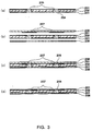
- a method of manufacturing a double-faced circuit board according to a second example of the present invention will be explained with reference to FIG. 3(a) - (d).
- through holes 204 were formed in an electrical insulating substrate 202 having adhesive layers 201 formed on its both surfaces and were filled with a conductive paste 205 as in the first example.
- a supporting base 206 provided with a wiring layer 207 formed in a predetermined form was superposed from one side of the substrate 202 so that at least the wiring layer 207 was positioned right above the through holes 204 filled with the conductive paste 205, and a copper foil 208 was superposed from the other side, which was then heated and pressurized by vacuum press.
- the heating and pressurization allowed the adhesive layers 201 to flow and thus the wiring layer 207 was embedded in the adhesive layer 201 on which the supporting base 206 had been superposed as shown in FIG. 3(c).
- the substrate 202 was deformed.
- the conductive paste 205 within the though holes 204 was compressed, and a resinous constituent contained in the conductive paste 205 flowed out in the adhesive layers 201. Therefore, the conductive constituent contained in the conductive paste 205 became dense, thus electrically connecting the wiring layer 207 positioned on one side and the copper foil 208 on the other side of the substrate 202.
- the adhesive layers 201 and the conductive paste 205 were cured.
- the supporting base 206 was removed while leaving the wiring layer 207 embedded in the adhesive layer 201 as shown in FIG. 3(d), thus completing a double-faced circuit board.
- the present example differs from the first example in that the conductive paste 205 is compressed from one side of the substrate 202.
- the thickness of a film as the electrical insulating substrate 202 is set to be 12 ⁇ m and the thickness of each adhesive layer 201 is set to be 5 ⁇ m as in the first example.
- the volume ratio of the resinous constituent and the conductive constituent in the conductive paste 205 was set to be about 50% considering print quality. Therefore, most of the resinous constituent in the conductive paste 205 within the through holes 204 was pressed out in the adhesive layers, and the conductive constituent became dense within the through holes 204, thus obtaining via holes with low resistance and high reliability. From experiments, when the volume compressibility was at least 20%, electric connection with low resistance could be obtained, thus improving the connection reliability.
- the total thickness of the adhesive layers 201 was substantially the same as the thickness of the wiring layer 207.
- the wiring layer is thicker than the adhesive layer, further excellent electric connection can be obtained.
- adhesives are received between conductors in the wiring layer. Therefore, when the wiring layer is too thick, the portions between the conductors cannot be filled.
- the increase in volume of deformation of the electrical insulating substrate is anticipated. The volume of deformation varies depending on the density of the wiring layer, i.e. a ratio of residual copper.
- any minute pores are acceptable as long as the pores are minute to such an extent that the conductive constituents in the conductive paste do not flow out.
- the conductive constituent is copper powder with a diameter of 10 ⁇ m
- minute pores with a diameter of about 5 ⁇ m are acceptable.
- a method of manufacturing a multilayer circuit board according to a third example of the present invention will be explained with reference to FIG. 4(a)-(e).
- a double-faced circuit board was manufactured as in the second example.
- Numerals 301 and 302 indicate adhesive layers and an electrical insulating substrate.
- a numeral 304 denotes through holes provided in the substrate 302. The through holes 304 are filled with a conductive pate 305. The conductive paste 305 within the through holes 304 is compressed from one side by a wiring Layer 307.
- a numeral 308 indicates a copper foil.
- an electrical insulating substrate 312 provided with adhesive layers 311 on its both surfaces and through holes 314 filled with a conductive paste 315 at predetermined positions was superposed together with a supporting base 316 with a wiring layer 317 formed in a predetermined pattern as shown in FIG. 4(b). Then, as shown in FIG. 4(c), it was heated and pressurized by vacuum press, thus electrically connecting the wiring layer 307 and the wiring layer 317. After that, as shown in FIG. 4(d), the supporting base 316 was removed. The steps shown in FIG. 4(b) - 4(d) were repeated for a predetermined number of times to laminate a predetermined number of layers. Then, as shown in FIG. 4(e), the copper foil 308 was etched in a predetermined shape, thus completing a multilayer circuit board.
- via holes for example, through holes 314.
- via holes for example, through holes 304
- increasing the wiring density since the surface from which the supporting base 316 has been removed is flat, even lamination of many layers does not cause unevenness on the surface, thus enabling a large number of layers to be laminated.
- the multilayer circuit board of the present invention has a smooth surface and is therefore convenient for mounting semiconductor bare chips.
- the flatness of the actually manufactured multilayer circuit board was ⁇ 5 ⁇ m in a square with sides of 10mm in the area where the semiconductor bare chips were to be mounted, which was extremely flat. When semiconductor bare chips were mounted face down, the mounting yield was good due to the excellent flatness of the surface under the chips, thus improving mounting reliability.
- the layers are laminated on the copper foil 308. Therefore, a change in size after the lamination can be restrained. Thus, dislocation can be suppressed even in the case where a large number of layers are laminated, which enables the design with a precise design rule.
- a nickel layer with a thickness of about 3 ⁇ m having no pin hole or the like was formed as an etching-stopper layer 22 on the copper foil 26 by plating, deposition, bonding, or the like.
- a metal layer 21 made of copper as a wiring layer material was formed on the nickel layer 22 by plating, deposition, bonding, or the like.
- the metal layer 21 is required to have a thickness that satisfies electric characteristics as a wiring layer, is not affected by side etching or the like in a later etching step, and thus enables a minute pattern to be formed. Considering this, the metal layer 21 was formed to be about 10 ⁇ m in the present production method.
- a substrate 23 formed of a PET film was bonded to the surface of the supporting base 26 opposite the surface on which the nickel layer 22 and the copper layer 21 had been laminated, using an adhesive 24 containing a foaming agent (FIG. 5(b)).
- the copper of the metal layer 21 of the top surface was photo-etched to form a wiring layer 27 with a desired pattern (FIG. 5(c)).
- an ammonium persulfate solution was used as an etchant.
- the nickel of the etching-stopper layer 22 was not etched by the ammonium persulfate solution, only the copper of the metal layer 21 was etched.
- the copper of the supporting base 26 was protected by the substrate 23 from the back side and therefore was not attacked at all.
- the layered product obtained in the present production method was used instead of each supporting base 106 with the wiring layer 107 in the first example and was heated and pressurized as in the first example.
- the wiring layers 27 were embedded in the adhesive layers 101, and the wiring layers 27 on both the surfaces of the electrical insulating substrate 102 were electrically connected to each other.
- the copper of the supporting substrates 26 was etched using an ammonium persulfate solution and then the nickel layer 22 was etched using a hydrochloric acid solution to be removed separately, thus obtaining a double-faced circuit board in which the wiring layers 27 had been embedded in the adhesive layers 101.
- the supporting substrate 26 was used for the supporting substrate 26.
- any material can be used as long as the etchant used for the material is different from that used for the etching-stopper layer 22. Therefore, aluminum may be used.
- the etching-stopper layer 22 iron, chromium, or the like can be used instead of nickel. Depending on the selection of the etchants, the respective materials can be combined variously.
- the steps of embedding the wiring layers 27 in the adhesive layers 101 and separating the substrates 23 can be carried out simultaneously by: laminating the layered bodies in the state shown in FIG. 5(c) on the electrical insulating substrate 102 without peeling and removing the substrates 23 by heating (see FIG. 1 (f)); and when heating and pressurizing it, increasing temperature to at least a temperature that enables the foaming agent contained in the adhesive 24 to foam.
- a substrate 33 was bonded to the back surface of a supporting base 36 made of aluminum using an adhesive 34 containing a foaming agent.
- a photosensitive resin layer as the insulating material was formed to have a thickness of about 10 ⁇ m.
- the photosensitive resin layer can be formed by spinner, roll coat, or the like.
- the photosensitive resin layer was exposed and developed using a mask with a desired pattern, thus forming a photosensitive resin pattern 38 on the surface of the supporting base 36 (FIG. 6(b)).
- the exposed surface of the supporting base 36 was copper-plated to form a wiring layer 37 made of copper having a desired pattern (FIG. 6(c)).
- the electroplating enables copper easily to adhere selectively onto only the area where the surface of the supporting base 36 is exposed.
- the etching-stopper layer explained in Production Method 1 may be laminated between the supporting base 36 and the photosensitive resin pattern 38.
- the etching-stopper layer must be made of a conductive material.
- the photosensitive resin pattern 38 was removed using a sodium hydroxide solution of about 3 wt% (FIG. 6(d)).
- the temperature was increased to a predetermined temperature by heating to allow the foaming agent contained in the adhesive 34 to foam, thus peeling off the substrate 33.
- the supporting base 36 on which the wiring layer 37 formed of copper had been formed in a desired pattern was obtained (FIG. 6(e)).
- the adhesion of the copper by plating in the present production method enables the pattern formation precisely according to a resist pattern, since side etching is not caused as in etching.
- the present production method is advantageous in forming a minute pattern.
- the layered body in the state shown in FIG. 6(d) may be laminated on an electrical insulating substrate without peeling and removing the substrate 33 by heating and then may be heated and pressurized to peel off the substrate 33 as in Production Method 1.
- a method of manufacturing a multilayer circuit board according to a fourth example of the present invention will be explained with reference to FIG. 7.
- a multilayer circuit board 410 produced as in the third example and a core substrate 411 having a predetermined number of insulating layers and wiring layers were prepared.
- the present example will be explained by an example using the multilayer circuit board explained in the conventional example as the core substrate 411.
- the multilayer circuit board 410 and the core substrate 411 were superposed with an electrical insulating substrate 402 being sandwiched therebetween.
- the substrate 402 has adhesive layers 401 on its both surfaces and through holes 404 filled with a conductive paste 405 at predetermined positions.
- the substrate 402 was obtained by carrying out the same steps as those shown in FIG. 1(a)-(e) in the first example. After that, as shown in FIG.
- a conductor 427 on the top layer of the core substrate 411 was embedded in the adhesive layer 401 by heating and pressurization to compress the conductive paste 405 within the through holes 404.
- the multilayer circuit board 410 and the core substrate 411 were electrically connected to each other.
- a copper foil 408 of the top layer of the multilayer circuit board 410 was etched selectively in a predetermined shape, thus completing a multilayer circuit board with a minute wiring pattern on its top layer.
- the above-mentioned multilayer circuit board is excellent in the wiring formation at a high density.
- the wiring density was further increased by providing the minute wiring pattern on the top layer.
- minute wiring corresponding to its pad pitch is required on the top layer.
- the above-mentioned multilayer circuit board is suitable even for mounting such semiconductor bare chips.
- the multilayer circuit board 410 was provided on one surface of the above-mentioned multilayer circuit board as the core substrate 411. However, it is advantageous in preventing warp or the like of the whole wiring board to provide the multilayer circuit boards 410 on both the surfaces.
- the core substrate 411 is not limited to that.
- a glass epoxy multilayer circuit board can be used as the core substrate 411.
- the following effects are obtained.
- a film base with high heat-resistance and high stiffness can be used as described in the first to third examples. Therefore, the multilayer circuit board can withstand a heat treatment in mounting semiconductor bare chips, and the change in size also can be restrained.
- the multilayer circuit board 410 of the top layer and the core substrate 411 can be manufactured and tested separately. Therefore, the general yield can be improved. Furthermore, since an electrical insulating substrate with minute through holes is used as a connecting member, positioning accuracy is not strictly limited, which enables easy manufacture.
- the wiring layer 427 of the top layer of the core substrate 411 was embedded in the adhesive layer 401.
- the multilayer circuit board shown in FIG. 4(e) that was manufactured as in the third example may be laminated with the wiring layer formed of a copper foil 308 that has been selectively etched facing the electrical insulating substrate 402.
- the wiring layer of the top layer of the substrate 410 is embedded in the adhesive layer 401. Consequently, the wiring layer formed of the copper foil 308 can compress the conductive paste 405 within the through holes 404, thus obtaining the same effect as the above.
- the supporting base 316 can be removed at the end after embedding the wiring layer 308 of the top layer of the multilayer circuit board 410 in the adhesive layer 401 by heating and pressurization without removing the supporting base 316.
- the supporting base 316 protects the minute wiring layer of the top layer until the step just before completing the multilayer circuit board of the present example including the heating and pressurizing step. Therefore, it is advantageous in manufacture.
- both the wiring layer 427 of the top layer of the core substrate 411 and the wiring layer 308 of the top layer of the multilayer circuit board 410 may be embedded in the adhesive layers 401.
- the conductive paste 405 within the through holes 404 is compressed from both sides. As a result, the amount of compressing the conductive paste increases, thus further improving the reliability in connection by the conductive paste.
- a multilayer circuit board was manufactured using a substrate bonding body having compressibility, which has through holes filled with a conductive paste and formed at predetermined positions, instead of the electrical insulating substrate 402 having adhesive layers on its both surfaces and the through holes 404 filled with the conductive paste 405 in the fourth example.
- an electrical insulating material for example, a glass epoxy resin, a phenol resin, a polyimide resin, a polyester resin, an aramide resin, or the like
- a pre-preg formed by impregnating an aramide nonwoven fabric with epoxy resin and bringing it into a semi-cured state (in a B stage state) can be used in general.
- the through holes are filled with a conductive paste containing a conductive constituent such as Ag, Cu, an alloy of Ag and Cu, or the like.
- the conductive paste when the conductive paste is formed so as to protrude from the surfaces of the substrate bonding body, the conductive paste is compressed favorably. Consequently, the multilayer circuit board 410 and the core substrate 411 can be electrically connected with low resistance.
- a pre-preg with a thickness of about 0.1mm that was obtained by impregnating a nonwoven fabric formed of aramid fibers with an epoxy resin was processed to have through holes at desired positions using a CO 2 laser. Then, the through holes were filled with a Cu paste so that the Cu paste protruded from the surfaces slightly.
- the multilayer circuit board 410, the aforementioned substrate bonding body, and the core substrate 411 were heated to be compressed at a temperature of 200°C and a pressure of 45-55 kg/cm 2 for 60 minutes.
- the conductor 427 that protruded from the surface of the core substrate 411 was immersed into the epoxy resin of the substrate bonding body.
- the conductive paste was sandwiched by the wiring layer of the multilayer circuit board 410 and the conductor 427 on the surface of the core substrate 411. Therefore, the conductive paste filling the inside the through holes was compressed, thus electrically connecting the wiring layer and the conductor 427.
- the conductor 427 protruding from the surface of the core substrate 411 was embedded in the substrate bonding body.
- a wiring layer protruding from the surface of the multilayer circuit board 410 to be laminated may be preformed, which provides the same effect.
- both the conductor 427 protruding from the surface of the core substrate 411 and the wiring layer protruding from the surface of the multilayer circuit board 410 may be embedded in the substrate bonding body.
- the conductive paste within the though holes is compressed from both sides. As a result, the amount of compressing of the conductive paste increases, thus further improving the reliability in connection by the conductive paste.
- the reliability in the connection by the conductive paste improves.
- a blackening process was carried out on the surface of the wiring layer of the multilayer circuit board 410 and the surface of the conductor 427 of the core substrate 411 using sodium hydroxide 15g/litre, sodium phosphate 12g/litre, and sodium chlorite 30g/litre, thus obtaining rough surfaces with a roughness of about 0.5 ⁇ m.
- a film produced on the surface of the copper foil by the blackening process is an insulating film. However, the insulating film is extremely thin and therefore is easily broken by heating and pressurization, thus enabling conduction.
- copper electroplating also can be employed. That is, a method in which copper is abnormally precipitated in a nodule shape by increasing current density to be higher than that of the condition for producing a copper foil has been well known in general. When using this method, a film produced on the surface of the copper foil is made of copper, thus obtaining further stable electric connection.
Applications Claiming Priority (6)
| Application Number | Priority Date | Filing Date | Title |
|---|---|---|---|
| JP13173198 | 1998-05-14 | ||
| JP13173198 | 1998-05-14 | ||
| JP15958698 | 1998-06-08 | ||
| JP15958698A JP3172711B2 (ja) | 1998-06-08 | 1998-06-08 | 転写媒体とその製造方法及びその転写媒体を使った配線パターンの製造方法 |
| JP16814398 | 1998-06-16 | ||
| JP16814398 | 1998-06-16 |
Publications (3)
| Publication Number | Publication Date |
|---|---|
| EP0961533A2 true EP0961533A2 (fr) | 1999-12-01 |
| EP0961533A3 EP0961533A3 (fr) | 2001-04-11 |
| EP0961533B1 EP0961533B1 (fr) | 2006-05-10 |
Family
ID=27316359
Family Applications (1)
| Application Number | Title | Priority Date | Filing Date |
|---|---|---|---|
| EP99108632A Expired - Lifetime EP0961533B1 (fr) | 1998-05-14 | 1999-05-12 | Plaque à circuit et son procédé de fabrication |
Country Status (5)
| Country | Link |
|---|---|
| US (2) | US6197407B1 (fr) |
| EP (1) | EP0961533B1 (fr) |
| DE (1) | DE69931212T2 (fr) |
| SG (1) | SG86345A1 (fr) |
| TW (1) | TW507508B (fr) |
Cited By (11)
| Publication number | Priority date | Publication date | Assignee | Title |
|---|---|---|---|---|
| WO2001063989A1 (fr) * | 2000-02-22 | 2001-08-30 | Honeywell International Inc. | Structure de plis lies et procede associe permettant l'interconnexion de paires de couches conductrices au moyen d'encres conductrices |
| EP1180920A2 (fr) | 2000-08-17 | 2002-02-20 | Matsushita Electric Industrial Co., Ltd. | Panneau à circuit et son procédé de fabrication |
| EP1213952A2 (fr) * | 2000-12-05 | 2002-06-12 | Matsushita Electric Industrial Co., Ltd. | Substrat à circuit et son procédé de fabrication |
| EP1220586A2 (fr) * | 2000-12-28 | 2002-07-03 | Nitto Denko Corporation | Préimprégné pour panneau à circuit et son procédé de fabrication |
| US6459046B1 (en) | 2000-08-28 | 2002-10-01 | Matsushita Electric Industrial Co., Ltd. | Printed circuit board and method for producing the same |
| EP1194020A3 (fr) * | 2000-09-27 | 2004-03-31 | Matsushita Electric Industrial Co., Ltd. | Panneau de résine, procédé de fabrication d'une panneau de résine, corps à interconnexions, panneau à circuit et procédé de fabrication d'un panneau à circuit |
| EP1791409A1 (fr) * | 2005-11-29 | 2007-05-30 | TDK Corporation | Carte de circuit multicouche et son procédé de fabrication |
| US7321496B2 (en) | 2004-03-19 | 2008-01-22 | Matsushita Electric Industrial Co., Ltd. | Flexible substrate, multilayer flexible substrate and process for producing the same |
| WO2008109412A1 (fr) * | 2007-03-02 | 2008-09-12 | Raytheon Company | Procédé pour fabriquer un circuit électrique sur des films plastiques ultra-fins |
| US20140338192A1 (en) * | 2011-12-23 | 2014-11-20 | Inktec Co., Ltd. | Method for manufacturing a metal printed circuit board |
| CN104538314A (zh) * | 2014-12-29 | 2015-04-22 | 华进半导体封装先导技术研发中心有限公司 | 三层封装基板及封装芯片的制作方法及三层封装基板 |
Families Citing this family (55)
| Publication number | Priority date | Publication date | Assignee | Title |
|---|---|---|---|---|
| US6703565B1 (en) | 1996-09-06 | 2004-03-09 | Matsushita Electric Industrial Co., Ltd. | Printed wiring board |
| SG86345A1 (en) * | 1998-05-14 | 2002-02-19 | Matsushita Electric Ind Co Ltd | Circuit board and method of manufacturing the same |
| US6565954B2 (en) | 1998-05-14 | 2003-05-20 | Matsushita Electric Industrial Co., Ltd. | Circuit board and method of manufacturing the same |
| US6451441B1 (en) * | 1999-03-30 | 2002-09-17 | Kyocera Corporation | Film with metal foil |
| JP2001284783A (ja) * | 2000-03-30 | 2001-10-12 | Shinko Electric Ind Co Ltd | 表面実装用基板及び表面実装構造 |
| US6753483B2 (en) * | 2000-06-14 | 2004-06-22 | Matsushita Electric Industrial Co., Ltd. | Printed circuit board and method of manufacturing the same |
| EP1300708A1 (fr) * | 2000-07-10 | 2003-04-09 | Hikari Tech Co. Ltd. | Procede de fabrication d'une ferrule a plusieurs corps |
| US6518514B2 (en) * | 2000-08-21 | 2003-02-11 | Matsushita Electric Industrial Co., Ltd. | Circuit board and production of the same |
| US6757176B1 (en) * | 2000-08-22 | 2004-06-29 | Micron Technology, Inc. | Circuit board |
| JP2002319761A (ja) * | 2001-04-23 | 2002-10-31 | Nitto Denko Corp | 配線基板の製造方法 |
| JP3840921B2 (ja) * | 2001-06-13 | 2006-11-01 | 株式会社デンソー | プリント基板のおよびその製造方法 |
| JP2003008201A (ja) * | 2001-06-18 | 2003-01-10 | Nitto Denko Corp | 金属箔積層体の製造方法及び配線基板の製造方法 |
| US6921869B2 (en) * | 2001-09-26 | 2005-07-26 | Fujikura Ltd. | Interlayer connection structure of multilayer wiring board, method of manufacturing method of forming land thereof |
| JP2003133727A (ja) * | 2001-10-22 | 2003-05-09 | Nec Toppan Circuit Solutions Inc | 樹脂穴埋め基板の製造方法およびそれを用いた多層プリント配線板の製造方法 |
| TW545092B (en) * | 2001-10-25 | 2003-08-01 | Matsushita Electric Ind Co Ltd | Prepreg and circuit board and method for manufacturing the same |
| MY140754A (en) * | 2001-12-25 | 2010-01-15 | Hitachi Chemical Co Ltd | Connection board, and multi-layer wiring board, substrate for semiconductor package and semiconductor package using connection board, and manufacturing method thereof |
| JP3823870B2 (ja) * | 2002-04-22 | 2006-09-20 | セイコーエプソン株式会社 | 配線板の製造方法、および電子機器の製造方法 |
| EP1357773A3 (fr) * | 2002-04-25 | 2005-11-30 | Matsushita Electric Industrial Co., Ltd. | Feuille de transfert de câblage et son procédé de fabrication, et panneau de câblage et son procédé de fabrication |
| TW530377B (en) * | 2002-05-28 | 2003-05-01 | Via Tech Inc | Structure of laminated substrate with high integration and method of production thereof |
| US7438969B2 (en) * | 2002-07-10 | 2008-10-21 | Ngk Spark Plug Co., Ltd. | Filling material, multilayer wiring board, and process of producing multilayer wiring board |
| WO2004014114A1 (fr) * | 2002-07-31 | 2004-02-12 | Sony Corporation | Procede de realisation de carte a dispositif integre, carte a dispositif integre, procede de realisation de carte imprimee, carte imprimee |
| US6703114B1 (en) * | 2002-10-17 | 2004-03-09 | Arlon | Laminate structures, methods for production thereof and uses therefor |
| CA2418683C (fr) * | 2003-02-11 | 2007-01-02 | Ibm Canada Limited - Ibm Canada Limitee | Reseau avec dispositif de connexion a faible inductance |
| CN100438724C (zh) * | 2003-03-03 | 2008-11-26 | 精工爱普生株式会社 | 布线基板的制造方法 |
| US7930815B2 (en) * | 2003-04-11 | 2011-04-26 | Avery Dennison Corporation | Conductive pattern and method of making |
| TW200505304A (en) * | 2003-05-20 | 2005-02-01 | Matsushita Electric Ind Co Ltd | Multilayer circuit board and method for manufacturing the same |
| US6913952B2 (en) * | 2003-07-03 | 2005-07-05 | Micron Technology, Inc. | Methods of forming circuit traces and contact pads for interposers utilized in semiconductor packages |
| US20050124197A1 (en) * | 2003-12-04 | 2005-06-09 | Matsushita Electric Industrial Co., Ltd. | Circuit board and method for manufacturing the same, semiconductor package, component built-in module and board for electronic equipment |
| US20050230821A1 (en) * | 2004-04-15 | 2005-10-20 | Kheng Lee T | Semiconductor packages, and methods of forming semiconductor packages |
| US20050285253A1 (en) * | 2004-06-24 | 2005-12-29 | Kumamoto Takashi | Forming buried via hole substrates |
| US20060068576A1 (en) * | 2004-09-30 | 2006-03-30 | Burdick William E Jr | Lithography transfer for high density interconnect circuits |
| US7976956B2 (en) * | 2005-08-01 | 2011-07-12 | Furukawa Circuit Foil., Ltd. | Laminated circuit board |
| US20070048507A1 (en) * | 2006-08-01 | 2007-03-01 | Furukawa Circuit Foil Co., Ltd. | Laminated circuit board |
| JP2007129124A (ja) * | 2005-11-07 | 2007-05-24 | Matsushita Electric Ind Co Ltd | 多層プリント配線基板及びその製造方法 |
| JP2007144626A (ja) * | 2005-11-24 | 2007-06-14 | Nitto Denko Corp | 導体張積層板、配線回路基板およびその製造方法 |
| US7523545B2 (en) | 2006-04-19 | 2009-04-28 | Dynamic Details, Inc. | Methods of manufacturing printed circuit boards with stacked micro vias |
| GB0619539D0 (en) * | 2006-10-04 | 2006-11-15 | Hexcel Composites Ltd | Curable resin films |
| US7451540B2 (en) * | 2006-10-24 | 2008-11-18 | Motorola, Inc. | Method for fabricating a printed circuit board |
| JP4873160B2 (ja) * | 2007-02-08 | 2012-02-08 | トヨタ自動車株式会社 | 接合方法 |
| US7918018B2 (en) * | 2007-06-12 | 2011-04-05 | Texas Instruments Incorporated | Method of fabricating a semiconductor device |
| KR101164598B1 (ko) * | 2007-10-16 | 2012-07-10 | 삼성테크윈 주식회사 | 다층 회로기판의 제조 방법 |
| SG155096A1 (en) | 2008-03-03 | 2009-09-30 | Micron Technology Inc | Board-on-chip type substrates with conductive traces in multiple planes, semiconductor device packages including such substrates, and associated methods |
| JP5589835B2 (ja) * | 2008-03-26 | 2014-09-17 | 住友ベークライト株式会社 | 銅箔付き樹脂シート、多層プリント配線板、多層プリント配線板の製造方法および半導体装置 |
| JP4768059B2 (ja) * | 2009-08-12 | 2011-09-07 | タツタ電線株式会社 | 多層フレキシブルプリント配線板 |
| CN106455369A (zh) * | 2010-06-03 | 2017-02-22 | Ddi环球有限公司 | 利用盲过孔和内部微过孔以耦联子组件来制造印刷电路板的系统和方法 |
| US9326378B2 (en) * | 2011-08-29 | 2016-04-26 | Kyocera Corporation | Thin-film wiring substrate and substrate for probe card |
| US8623226B2 (en) * | 2012-04-12 | 2014-01-07 | Eastman Kodak Company | Making stacked pancake motors using patterned adhesives |
| JP5888260B2 (ja) * | 2012-05-30 | 2016-03-16 | 株式会社デンソー | 発熱装置 |
| US9899330B2 (en) * | 2014-10-03 | 2018-02-20 | Mc10, Inc. | Flexible electronic circuits with embedded integrated circuit die |
| TWI775905B (zh) * | 2017-07-25 | 2022-09-01 | 日商松下知識產權經營股份有限公司 | 多層印刷配線板之製造方法 |
| CN213522492U (zh) * | 2017-11-16 | 2021-06-22 | 株式会社村田制作所 | 树脂多层基板、电子部件及其安装构造 |
| WO2019098011A1 (fr) * | 2017-11-16 | 2019-05-23 | 株式会社村田製作所 | Substrat multicouche en résine, composant électronique et structure de montage pour composant électronique |
| CN112312671B (zh) * | 2019-07-30 | 2024-03-12 | 宏恒胜电子科技(淮安)有限公司 | 电路板以及电路板的制备方法 |
| US11310921B2 (en) | 2019-10-23 | 2022-04-19 | International Business Machines Corporation | Buried via in a circuit board |
| CN113784548B (zh) * | 2021-08-10 | 2024-04-16 | 深圳市信维通信股份有限公司 | 三明治胶层制备方法及多层线路板制备方法 |
Citations (5)
| Publication number | Priority date | Publication date | Assignee | Title |
|---|---|---|---|---|
| EP0568930A2 (fr) * | 1992-05-06 | 1993-11-10 | Matsushita Electric Industrial Co., Ltd. | Procédé de fabrication d'un substrat organique pour des circuits imprimés |
| JPH0621619A (ja) * | 1992-07-03 | 1994-01-28 | Matsushita Electric Ind Co Ltd | プリント配線板およびその形成方法 |
| US5407511A (en) * | 1991-02-19 | 1995-04-18 | Matsushita Electric Industrial Co., Ltd. | Process for forming a sintered conductor circuit board |
| JPH07147464A (ja) * | 1993-09-21 | 1995-06-06 | Matsushita Electric Ind Co Ltd | 回路基板接続材とそれを用いた多層回路基板の製造方法 |
| JPH1084186A (ja) * | 1996-09-06 | 1998-03-31 | Matsushita Electric Ind Co Ltd | 配線基板の製造方法並びに配線基板 |
Family Cites Families (47)
| Publication number | Priority date | Publication date | Assignee | Title |
|---|---|---|---|---|
| US3264402A (en) | 1962-09-24 | 1966-08-02 | North American Aviation Inc | Multilayer printed-wiring boards |
| FR2134436B1 (fr) | 1971-04-28 | 1975-06-20 | It | |
| JPS5317970A (en) | 1976-08-04 | 1978-02-18 | Fujitsu Ltd | Copper stacking board |
| US4383363A (en) * | 1977-09-01 | 1983-05-17 | Sharp Kabushiki Kaisha | Method of making a through-hole connector |
| US4648179A (en) | 1983-06-30 | 1987-03-10 | International Business Machines Corporation | Process of making interconnection structure for semiconductor device |
| FR2555808B1 (fr) | 1983-11-25 | 1986-10-10 | Videocolor | Masque d'ombre pour tube d'image en couleurs et tube d'image le comportant |
| US5707925A (en) | 1986-04-11 | 1998-01-13 | Dai Nippon Insatsu Kabushiki Kaisha | Image formation on objective bodies |
| JPS6356991A (ja) | 1986-08-27 | 1988-03-11 | 三井金属鉱業株式会社 | プリント配線板の製造法 |
| JPS63312983A (ja) | 1987-06-16 | 1988-12-21 | Hitachi Ltd | 無電解銅めっき方法 |
| JPS6484186A (en) | 1987-09-28 | 1989-03-29 | Hitachi Ltd | Nuclear reactor |
| JPH02283094A (ja) | 1989-04-25 | 1990-11-20 | Furukawa Electric Co Ltd:The | アルミパッド付き回路基板の製造方法 |
| JPH03183545A (ja) | 1989-12-14 | 1991-08-09 | Teijin Ltd | 制電易接着性フイルム、その製造方法及びそれを用いた磁気カード |
| US5046238A (en) | 1990-03-15 | 1991-09-10 | Rogers Corporation | Method of manufacturing a multilayer circuit board |
| DE69233232T2 (de) | 1991-02-22 | 2004-08-05 | Canon K.K. | Elektrischer Verbindungskörper und Herstellungsverfahren dafür |
| DE4119481A1 (de) | 1991-06-13 | 1992-12-17 | Nokia Deutschland Gmbh | Masken-rahmen-kombination fuer eine farbbildroehre |
| US5374469A (en) | 1991-09-19 | 1994-12-20 | Nitto Denko Corporation | Flexible printed substrate |
| JP3057924B2 (ja) | 1992-09-22 | 2000-07-04 | 松下電器産業株式会社 | 両面プリント基板およびその製造方法 |
| JPH06318783A (ja) | 1993-05-10 | 1994-11-15 | Meikoo:Kk | 多層回路基板の製造方法 |
| JP3087152B2 (ja) | 1993-09-08 | 2000-09-11 | 富士通株式会社 | 樹脂フィルム多層回路基板の製造方法 |
| EP0645950B1 (fr) * | 1993-09-21 | 1998-09-02 | Matsushita Electric Industrial Co., Ltd. | Pièce de connexion d'un substrat à circuit et procédé de fabrication de substrats à circuit multicouches en l'utilisant |
| US5652042A (en) | 1993-10-29 | 1997-07-29 | Matsushita Electric Industrial Co., Ltd. | Conductive paste compound for via hole filling, printed circuit board which uses the conductive paste |
| US5480503A (en) | 1993-12-30 | 1996-01-02 | International Business Machines Corporation | Process for producing circuitized layers and multilayer ceramic sub-laminates and composites thereof |
| US5456004A (en) * | 1994-01-04 | 1995-10-10 | Dell Usa, L.P. | Anisotropic interconnect methodology for cost effective manufacture of high density printed circuit boards |
| US6137054A (en) | 1994-01-25 | 2000-10-24 | Yazaki Corporation | Wire-circuit sheet and electric junction box thereof |
| JP3207663B2 (ja) | 1994-03-22 | 2001-09-10 | 松下電器産業株式会社 | プリント配線基板及びその製造方法 |
| US5595943A (en) | 1994-06-30 | 1997-01-21 | Hitachi, Ltd. | Method for formation of conductor using electroless plating |
| US5498467A (en) * | 1994-07-26 | 1996-03-12 | W. L. Gore & Associates, Inc. | Process for preparing selectively conductive materials by electroless metal deposition and product made therefrom |
| US5719354A (en) | 1994-09-16 | 1998-02-17 | Hoechst Celanese Corp. | Monolithic LCP polymer microelectronic wiring modules |
| JPH08229887A (ja) | 1994-12-27 | 1996-09-10 | Seiko Epson Corp | 積層シートのカット方法およびその装置 |
| JP3311899B2 (ja) | 1995-01-20 | 2002-08-05 | 松下電器産業株式会社 | 回路基板及びその製造方法 |
| JP2807976B2 (ja) * | 1995-02-14 | 1998-10-08 | ニッコー株式会社 | 導体充填スルーホールの製造方法 |
| JP3290041B2 (ja) | 1995-02-17 | 2002-06-10 | インターナショナル・ビジネス・マシーンズ・コーポレーション | 多層プリント基板、多層プリント基板の製造方法 |
| JPH08287840A (ja) | 1995-04-14 | 1996-11-01 | Toshiba Corp | カラー受像管 |
| JPH08298078A (ja) | 1995-04-28 | 1996-11-12 | Toshiba Corp | カラー受像管 |
| JPH0936551A (ja) * | 1995-05-15 | 1997-02-07 | Ibiden Co Ltd | 多層プリント配線板用片面回路基板、および多層プリント配線板とその製造方法 |
| JPH08213757A (ja) | 1995-06-26 | 1996-08-20 | Hitachi Chem Co Ltd | 配線板の製造法 |
| JPH09116273A (ja) * | 1995-08-11 | 1997-05-02 | Shinko Electric Ind Co Ltd | 多層回路基板及びその製造方法 |
| JP2736042B2 (ja) * | 1995-12-12 | 1998-04-02 | 山一電機株式会社 | 回路基板 |
| JP3492467B2 (ja) | 1996-06-20 | 2004-02-03 | イビデン株式会社 | 多層プリント配線板用片面回路基板、および多層プリント配線板とその製造方法 |
| US6143116A (en) | 1996-09-26 | 2000-11-07 | Kyocera Corporation | Process for producing a multi-layer wiring board |
| US6353189B1 (en) | 1997-04-16 | 2002-03-05 | Kabushiki Kaisha Toshiba | Wiring board, wiring board fabrication method, and semiconductor package |
| TW367519B (en) | 1997-05-27 | 1999-08-21 | Matsushita Electric Ind Co Ltd | Shielding plate body, shielding plate and color picture tube |
| JP3961092B2 (ja) | 1997-06-03 | 2007-08-15 | 株式会社東芝 | 複合配線基板、フレキシブル基板、半導体装置、および複合配線基板の製造方法 |
| KR100361565B1 (ko) | 1997-07-08 | 2002-11-22 | 이비덴 가부시키가이샤 | 인쇄 배선판 및 이의 제조방법 |
| WO1999034654A1 (fr) | 1997-12-29 | 1999-07-08 | Ibiden Co., Ltd. | Plaquette a circuits imprimes multicouche |
| SG86345A1 (en) * | 1998-05-14 | 2002-02-19 | Matsushita Electric Ind Co Ltd | Circuit board and method of manufacturing the same |
| US6224965B1 (en) | 1999-06-25 | 2001-05-01 | Honeywell International Inc. | Microfiber dielectrics which facilitate laser via drilling |
-
1999
- 1999-04-30 SG SG9901999A patent/SG86345A1/en unknown
- 1999-05-03 TW TW088107133A patent/TW507508B/zh not_active IP Right Cessation
- 1999-05-04 US US09/304,714 patent/US6197407B1/en not_active Expired - Lifetime
- 1999-05-12 DE DE69931212T patent/DE69931212T2/de not_active Expired - Lifetime
- 1999-05-12 EP EP99108632A patent/EP0961533B1/fr not_active Expired - Lifetime
-
2000
- 2000-02-15 US US09/504,570 patent/US6532651B1/en not_active Expired - Lifetime
Patent Citations (5)
| Publication number | Priority date | Publication date | Assignee | Title |
|---|---|---|---|---|
| US5407511A (en) * | 1991-02-19 | 1995-04-18 | Matsushita Electric Industrial Co., Ltd. | Process for forming a sintered conductor circuit board |
| EP0568930A2 (fr) * | 1992-05-06 | 1993-11-10 | Matsushita Electric Industrial Co., Ltd. | Procédé de fabrication d'un substrat organique pour des circuits imprimés |
| JPH0621619A (ja) * | 1992-07-03 | 1994-01-28 | Matsushita Electric Ind Co Ltd | プリント配線板およびその形成方法 |
| JPH07147464A (ja) * | 1993-09-21 | 1995-06-06 | Matsushita Electric Ind Co Ltd | 回路基板接続材とそれを用いた多層回路基板の製造方法 |
| JPH1084186A (ja) * | 1996-09-06 | 1998-03-31 | Matsushita Electric Ind Co Ltd | 配線基板の製造方法並びに配線基板 |
Non-Patent Citations (3)
| Title |
|---|
| PATENT ABSTRACTS OF JAPAN vol. 018, no. 230 (E-1542), 26 April 1994 (1994-04-26) -& JP 06 021619 A (MATSUSHITA ELECTRIC IND CO LTD), 28 January 1994 (1994-01-28) * |
| PATENT ABSTRACTS OF JAPAN vol. 1995, no. 09, 31 October 1995 (1995-10-31) & JP 07 147464 A (MATSUSHITA ELECTRIC IND CO LTD), 6 June 1995 (1995-06-06) * |
| PATENT ABSTRACTS OF JAPAN vol. 1998, no. 08, 30 June 1998 (1998-06-30) -& JP 10 084186 A (MATSUSHITA ELECTRIC IND CO LTD), 31 March 1998 (1998-03-31) * |
Cited By (25)
| Publication number | Priority date | Publication date | Assignee | Title |
|---|---|---|---|---|
| US6576839B1 (en) | 2000-02-22 | 2003-06-10 | Honeywell International Inc. | Bond-ply structure for interconnection of circuit layer pairs with conductive inks |
| WO2001063989A1 (fr) * | 2000-02-22 | 2001-08-30 | Honeywell International Inc. | Structure de plis lies et procede associe permettant l'interconnexion de paires de couches conductrices au moyen d'encres conductrices |
| EP1180920A2 (fr) | 2000-08-17 | 2002-02-20 | Matsushita Electric Industrial Co., Ltd. | Panneau à circuit et son procédé de fabrication |
| US6993836B2 (en) | 2000-08-17 | 2006-02-07 | Matsushita Electric Industrial Co., Ltd. | Circuit board and method of manufacturing same |
| EP1180920A3 (fr) * | 2000-08-17 | 2005-12-07 | Matsushita Electric Industrial Co., Ltd. | Panneau à circuit et son procédé de fabrication |
| US6799369B2 (en) | 2000-08-28 | 2004-10-05 | Matsushita Electric Industrial Co., Ltd. | Printed circuit board and method for producing the same |
| US6459046B1 (en) | 2000-08-28 | 2002-10-01 | Matsushita Electric Industrial Co., Ltd. | Printed circuit board and method for producing the same |
| EP1194020A3 (fr) * | 2000-09-27 | 2004-03-31 | Matsushita Electric Industrial Co., Ltd. | Panneau de résine, procédé de fabrication d'une panneau de résine, corps à interconnexions, panneau à circuit et procédé de fabrication d'un panneau à circuit |
| EP1213952A3 (fr) * | 2000-12-05 | 2004-06-30 | Matsushita Electric Industrial Co., Ltd. | Substrat à circuit et son procédé de fabrication |
| US6930395B2 (en) | 2000-12-05 | 2005-08-16 | Matsushita Electric Industrial Co., Ltd. | Circuit substrate having improved connection reliability and a method for manufacturing the same |
| EP1213952A2 (fr) * | 2000-12-05 | 2002-06-12 | Matsushita Electric Industrial Co., Ltd. | Substrat à circuit et son procédé de fabrication |
| EP1220586A3 (fr) * | 2000-12-28 | 2004-05-12 | Nitto Denko Corporation | Préimprégné pour panneau à circuit et son procédé de fabrication |
| EP1220586A2 (fr) * | 2000-12-28 | 2002-07-03 | Nitto Denko Corporation | Préimprégné pour panneau à circuit et son procédé de fabrication |
| US7773386B2 (en) | 2004-03-19 | 2010-08-10 | Panasonic Corporation | Flexible substrate, multilayer flexible substrate |
| US7321496B2 (en) | 2004-03-19 | 2008-01-22 | Matsushita Electric Industrial Co., Ltd. | Flexible substrate, multilayer flexible substrate and process for producing the same |
| EP1791409A1 (fr) * | 2005-11-29 | 2007-05-30 | TDK Corporation | Carte de circuit multicouche et son procédé de fabrication |
| US8188375B2 (en) | 2005-11-29 | 2012-05-29 | Tok Corporation | Multilayer circuit board and method for manufacturing the same |
| US8530752B2 (en) | 2005-11-29 | 2013-09-10 | Tdk Corporation | Multilayer circuit board and method for manufacturing the same |
| WO2008109412A1 (fr) * | 2007-03-02 | 2008-09-12 | Raytheon Company | Procédé pour fabriquer un circuit électrique sur des films plastiques ultra-fins |
| US8114576B2 (en) | 2007-03-02 | 2012-02-14 | Raytheon Company | Method for fabricating electrical circuitry on ultra-thin plastic films |
| US8535797B2 (en) | 2007-03-02 | 2013-09-17 | Raytheon Company | Method for fabricating electrical circuitry on ultra-thin plastic films |
| US20140338192A1 (en) * | 2011-12-23 | 2014-11-20 | Inktec Co., Ltd. | Method for manufacturing a metal printed circuit board |
| US10178773B2 (en) * | 2011-12-23 | 2019-01-08 | Inktec Co., Ltd. | Method for manufacturing a metal printed circuit board |
| CN104538314A (zh) * | 2014-12-29 | 2015-04-22 | 华进半导体封装先导技术研发中心有限公司 | 三层封装基板及封装芯片的制作方法及三层封装基板 |
| CN104538314B (zh) * | 2014-12-29 | 2017-08-11 | 华进半导体封装先导技术研发中心有限公司 | 三层封装基板及封装芯片的制作方法及三层封装基板 |
Also Published As
| Publication number | Publication date |
|---|---|
| EP0961533B1 (fr) | 2006-05-10 |
| TW507508B (en) | 2002-10-21 |
| SG86345A1 (en) | 2002-02-19 |
| DE69931212D1 (de) | 2006-06-14 |
| US6197407B1 (en) | 2001-03-06 |
| US6532651B1 (en) | 2003-03-18 |
| EP0961533A3 (fr) | 2001-04-11 |
| DE69931212T2 (de) | 2007-03-01 |
Similar Documents
| Publication | Publication Date | Title |
|---|---|---|
| EP0961533B1 (fr) | Plaque à circuit et son procédé de fabrication | |
| US6748652B2 (en) | Circuit board and method of manufacturing the same | |
| US6799369B2 (en) | Printed circuit board and method for producing the same | |
| US6946205B2 (en) | Wiring transfer sheet and method for producing the same, and wiring board and method for producing the same | |
| US6451710B1 (en) | Method of manufacturing multi-layer printed wiring board | |
| US7800917B2 (en) | Printed wiring board | |
| US7572500B2 (en) | Method of manufacturing circuit-forming board and material of circuit-forming board | |
| EP1180920B1 (fr) | Procédé de fabrication d'un panneau à circuit | |
| US7828924B2 (en) | Intermediate material for manufacturing circuit board and method for manufacturing circuit board using such intermediate material | |
| JP2004087856A (ja) | 多層配線基板 | |
| WO2001045478A1 (fr) | Carte a circuit imprime multicouche et procede de production | |
| US20040003494A1 (en) | Method of manufacturing multilayer wiring substrate, and multilayer wiring substrate | |
| JP4075673B2 (ja) | 多層プリント配線板用銅張り積層板、多層プリント配線板、多層プリント配線板の製造方法 | |
| JP3215090B2 (ja) | 配線基板、多層配線基板、及びそれらの製造方法 | |
| US6528733B2 (en) | Multi-layer circuit board and method of manufacturing same | |
| US5979044A (en) | Fabrication method of multilayer printed wiring board | |
| WO2006118141A1 (fr) | Carte de circuit imprimé multicouche et son procédé de fabrication | |
| JP4161604B2 (ja) | プリント配線板とその製造方法 | |
| JP3588888B2 (ja) | 多層プリント配線基板の製造方法 | |
| KR100607626B1 (ko) | 인쇄 회로 기판에 있어서 레진 도포된 동박을 이용한 평탄코팅 공법 | |
| WO2003032701A1 (fr) | Procede de fabrication d'une plaquette de circuit multicouche et plaquette de circuit multicouche obtenue par ce procede | |
| JP2000036664A (ja) | 多層配線基板およびその製造方法 |
Legal Events
| Date | Code | Title | Description |
|---|---|---|---|
| PUAI | Public reference made under article 153(3) epc to a published international application that has entered the european phase |
Free format text: ORIGINAL CODE: 0009012 |
|
| AK | Designated contracting states |
Kind code of ref document: A2 Designated state(s): DE FI FR GB SE |
|
| AX | Request for extension of the european patent |
Free format text: AL;LT;LV;MK;RO;SI |
|
| PUAL | Search report despatched |
Free format text: ORIGINAL CODE: 0009013 |
|
| AK | Designated contracting states |
Kind code of ref document: A3 Designated state(s): AT BE CH CY DE DK ES FI FR GB GR IE IT LI LU MC NL PT SE |
|
| AX | Request for extension of the european patent |
Free format text: AL;LT;LV;MK;RO;SI |
|
| RIN1 | Information on inventor provided before grant (corrected) |
Inventor name: TSUKAMOTO, MASAHIDE Inventor name: HIGASHITANI, HIDEKI Inventor name: NAKAMURA, TADASHI Inventor name: SUGAWA, TOSHIO Inventor name: ANDOU, DAIZOU |
|
| 17P | Request for examination filed |
Effective date: 20010412 |
|
| 17Q | First examination report despatched |
Effective date: 20010821 |
|
| AKX | Designation fees paid |
Free format text: DE FI FR GB SE |
|
| GRAP | Despatch of communication of intention to grant a patent |
Free format text: ORIGINAL CODE: EPIDOSNIGR1 |
|
| GRAS | Grant fee paid |
Free format text: ORIGINAL CODE: EPIDOSNIGR3 |
|
| GRAA | (expected) grant |
Free format text: ORIGINAL CODE: 0009210 |
|
| AK | Designated contracting states |
Kind code of ref document: B1 Designated state(s): DE FI FR GB SE |
|
| REG | Reference to a national code |
Ref country code: GB Ref legal event code: FG4D |
|
| REG | Reference to a national code |
Ref country code: SE Ref legal event code: TRGR |
|
| REF | Corresponds to: |
Ref document number: 69931212 Country of ref document: DE Date of ref document: 20060614 Kind code of ref document: P |
|
| ET | Fr: translation filed | ||
| PLBE | No opposition filed within time limit |
Free format text: ORIGINAL CODE: 0009261 |
|
| STAA | Information on the status of an ep patent application or granted ep patent |
Free format text: STATUS: NO OPPOSITION FILED WITHIN TIME LIMIT |
|
| 26N | No opposition filed |
Effective date: 20070213 |
|
| PGFP | Annual fee paid to national office [announced via postgrant information from national office to epo] |
Ref country code: GB Payment date: 20140507 Year of fee payment: 16 |
|
| PGFP | Annual fee paid to national office [announced via postgrant information from national office to epo] |
Ref country code: SE Payment date: 20140513 Year of fee payment: 16 Ref country code: FI Payment date: 20140512 Year of fee payment: 16 Ref country code: DE Payment date: 20140507 Year of fee payment: 16 Ref country code: FR Payment date: 20140509 Year of fee payment: 16 |
|
| REG | Reference to a national code |
Ref country code: DE Ref legal event code: R119 Ref document number: 69931212 Country of ref document: DE |
|
| GBPC | Gb: european patent ceased through non-payment of renewal fee |
Effective date: 20150512 |
|
| PG25 | Lapsed in a contracting state [announced via postgrant information from national office to epo] |
Ref country code: FI Free format text: LAPSE BECAUSE OF NON-PAYMENT OF DUE FEES Effective date: 20150512 |
|
| REG | Reference to a national code |
Ref country code: FR Ref legal event code: ST Effective date: 20160129 |
|
| PG25 | Lapsed in a contracting state [announced via postgrant information from national office to epo] |
Ref country code: SE Free format text: LAPSE BECAUSE OF NON-PAYMENT OF DUE FEES Effective date: 20150513 |
|
| PG25 | Lapsed in a contracting state [announced via postgrant information from national office to epo] |
Ref country code: GB Free format text: LAPSE BECAUSE OF NON-PAYMENT OF DUE FEES Effective date: 20150512 Ref country code: DE Free format text: LAPSE BECAUSE OF NON-PAYMENT OF DUE FEES Effective date: 20151201 |
|
| PG25 | Lapsed in a contracting state [announced via postgrant information from national office to epo] |
Ref country code: FR Free format text: LAPSE BECAUSE OF NON-PAYMENT OF DUE FEES Effective date: 20150601 |