EP0910121B1 - Semiconductor device - Google Patents
Semiconductor device Download PDFInfo
- Publication number
- EP0910121B1 EP0910121B1 EP96940147A EP96940147A EP0910121B1 EP 0910121 B1 EP0910121 B1 EP 0910121B1 EP 96940147 A EP96940147 A EP 96940147A EP 96940147 A EP96940147 A EP 96940147A EP 0910121 B1 EP0910121 B1 EP 0910121B1
- Authority
- EP
- European Patent Office
- Prior art keywords
- region
- mold resin
- lead frame
- package
- mold
- Prior art date
- Legal status (The legal status is an assumption and is not a legal conclusion. Google has not performed a legal analysis and makes no representation as to the accuracy of the status listed.)
- Expired - Lifetime
Links
Images


Classifications
-
- H—ELECTRICITY
- H01—ELECTRIC ELEMENTS
- H01L—SEMICONDUCTOR DEVICES NOT COVERED BY CLASS H10
- H01L24/00—Arrangements for connecting or disconnecting semiconductor or solid-state bodies; Methods or apparatus related thereto
- H01L24/01—Means for bonding being attached to, or being formed on, the surface to be connected, e.g. chip-to-package, die-attach, "first-level" interconnects; Manufacturing methods related thereto
- H01L24/02—Bonding areas ; Manufacturing methods related thereto
- H01L24/04—Structure, shape, material or disposition of the bonding areas prior to the connecting process
- H01L24/06—Structure, shape, material or disposition of the bonding areas prior to the connecting process of a plurality of bonding areas
-
- H—ELECTRICITY
- H01—ELECTRIC ELEMENTS
- H01L—SEMICONDUCTOR DEVICES NOT COVERED BY CLASS H10
- H01L21/00—Processes or apparatus adapted for the manufacture or treatment of semiconductor or solid state devices or of parts thereof
- H01L21/02—Manufacture or treatment of semiconductor devices or of parts thereof
- H01L21/04—Manufacture or treatment of semiconductor devices or of parts thereof the devices having at least one potential-jump barrier or surface barrier, e.g. PN junction, depletion layer or carrier concentration layer
- H01L21/50—Assembly of semiconductor devices using processes or apparatus not provided for in a single one of the subgroups H01L21/06 - H01L21/326, e.g. sealing of a cap to a base of a container
- H01L21/56—Encapsulations, e.g. encapsulation layers, coatings
- H01L21/565—Moulds
-
- H—ELECTRICITY
- H01—ELECTRIC ELEMENTS
- H01L—SEMICONDUCTOR DEVICES NOT COVERED BY CLASS H10
- H01L23/00—Details of semiconductor or other solid state devices
- H01L23/34—Arrangements for cooling, heating, ventilating or temperature compensation ; Temperature sensing arrangements
- H01L23/42—Fillings or auxiliary members in containers or encapsulations selected or arranged to facilitate heating or cooling
- H01L23/433—Auxiliary members in containers characterised by their shape, e.g. pistons
- H01L23/4334—Auxiliary members in encapsulations
-
- H—ELECTRICITY
- H01—ELECTRIC ELEMENTS
- H01L—SEMICONDUCTOR DEVICES NOT COVERED BY CLASS H10
- H01L23/00—Details of semiconductor or other solid state devices
- H01L23/48—Arrangements for conducting electric current to or from the solid state body in operation, e.g. leads, terminal arrangements ; Selection of materials therefor
- H01L23/488—Arrangements for conducting electric current to or from the solid state body in operation, e.g. leads, terminal arrangements ; Selection of materials therefor consisting of soldered or bonded constructions
- H01L23/495—Lead-frames or other flat leads
- H01L23/49575—Assemblies of semiconductor devices on lead frames
-
- H—ELECTRICITY
- H01—ELECTRIC ELEMENTS
- H01L—SEMICONDUCTOR DEVICES NOT COVERED BY CLASS H10
- H01L24/00—Arrangements for connecting or disconnecting semiconductor or solid-state bodies; Methods or apparatus related thereto
- H01L24/01—Means for bonding being attached to, or being formed on, the surface to be connected, e.g. chip-to-package, die-attach, "first-level" interconnects; Manufacturing methods related thereto
- H01L24/42—Wire connectors; Manufacturing methods related thereto
- H01L24/47—Structure, shape, material or disposition of the wire connectors after the connecting process
- H01L24/49—Structure, shape, material or disposition of the wire connectors after the connecting process of a plurality of wire connectors
-
- H—ELECTRICITY
- H01—ELECTRIC ELEMENTS
- H01L—SEMICONDUCTOR DEVICES NOT COVERED BY CLASS H10
- H01L2224/00—Indexing scheme for arrangements for connecting or disconnecting semiconductor or solid-state bodies and methods related thereto as covered by H01L24/00
- H01L2224/01—Means for bonding being attached to, or being formed on, the surface to be connected, e.g. chip-to-package, die-attach, "first-level" interconnects; Manufacturing methods related thereto
- H01L2224/02—Bonding areas; Manufacturing methods related thereto
- H01L2224/04—Structure, shape, material or disposition of the bonding areas prior to the connecting process
- H01L2224/04042—Bonding areas specifically adapted for wire connectors, e.g. wirebond pads
-
- H—ELECTRICITY
- H01—ELECTRIC ELEMENTS
- H01L—SEMICONDUCTOR DEVICES NOT COVERED BY CLASS H10
- H01L2224/00—Indexing scheme for arrangements for connecting or disconnecting semiconductor or solid-state bodies and methods related thereto as covered by H01L24/00
- H01L2224/01—Means for bonding being attached to, or being formed on, the surface to be connected, e.g. chip-to-package, die-attach, "first-level" interconnects; Manufacturing methods related thereto
- H01L2224/02—Bonding areas; Manufacturing methods related thereto
- H01L2224/04—Structure, shape, material or disposition of the bonding areas prior to the connecting process
- H01L2224/05—Structure, shape, material or disposition of the bonding areas prior to the connecting process of an individual bonding area
- H01L2224/0554—External layer
- H01L2224/0555—Shape
- H01L2224/05552—Shape in top view
- H01L2224/05553—Shape in top view being rectangular
-
- H—ELECTRICITY
- H01—ELECTRIC ELEMENTS
- H01L—SEMICONDUCTOR DEVICES NOT COVERED BY CLASS H10
- H01L2224/00—Indexing scheme for arrangements for connecting or disconnecting semiconductor or solid-state bodies and methods related thereto as covered by H01L24/00
- H01L2224/01—Means for bonding being attached to, or being formed on, the surface to be connected, e.g. chip-to-package, die-attach, "first-level" interconnects; Manufacturing methods related thereto
- H01L2224/02—Bonding areas; Manufacturing methods related thereto
- H01L2224/04—Structure, shape, material or disposition of the bonding areas prior to the connecting process
- H01L2224/06—Structure, shape, material or disposition of the bonding areas prior to the connecting process of a plurality of bonding areas
- H01L2224/0601—Structure
- H01L2224/0603—Bonding areas having different sizes, e.g. different heights or widths
-
- H—ELECTRICITY
- H01—ELECTRIC ELEMENTS
- H01L—SEMICONDUCTOR DEVICES NOT COVERED BY CLASS H10
- H01L2224/00—Indexing scheme for arrangements for connecting or disconnecting semiconductor or solid-state bodies and methods related thereto as covered by H01L24/00
- H01L2224/01—Means for bonding being attached to, or being formed on, the surface to be connected, e.g. chip-to-package, die-attach, "first-level" interconnects; Manufacturing methods related thereto
- H01L2224/42—Wire connectors; Manufacturing methods related thereto
- H01L2224/44—Structure, shape, material or disposition of the wire connectors prior to the connecting process
- H01L2224/45—Structure, shape, material or disposition of the wire connectors prior to the connecting process of an individual wire connector
- H01L2224/45001—Core members of the connector
- H01L2224/4501—Shape
- H01L2224/45012—Cross-sectional shape
- H01L2224/45015—Cross-sectional shape being circular
-
- H—ELECTRICITY
- H01—ELECTRIC ELEMENTS
- H01L—SEMICONDUCTOR DEVICES NOT COVERED BY CLASS H10
- H01L2224/00—Indexing scheme for arrangements for connecting or disconnecting semiconductor or solid-state bodies and methods related thereto as covered by H01L24/00
- H01L2224/01—Means for bonding being attached to, or being formed on, the surface to be connected, e.g. chip-to-package, die-attach, "first-level" interconnects; Manufacturing methods related thereto
- H01L2224/42—Wire connectors; Manufacturing methods related thereto
- H01L2224/44—Structure, shape, material or disposition of the wire connectors prior to the connecting process
- H01L2224/45—Structure, shape, material or disposition of the wire connectors prior to the connecting process of an individual wire connector
- H01L2224/45001—Core members of the connector
- H01L2224/45099—Material
- H01L2224/451—Material with a principal constituent of the material being a metal or a metalloid, e.g. boron (B), silicon (Si), germanium (Ge), arsenic (As), antimony (Sb), tellurium (Te) and polonium (Po), and alloys thereof
- H01L2224/45117—Material with a principal constituent of the material being a metal or a metalloid, e.g. boron (B), silicon (Si), germanium (Ge), arsenic (As), antimony (Sb), tellurium (Te) and polonium (Po), and alloys thereof the principal constituent melting at a temperature of greater than or equal to 400°C and less than 950°C
- H01L2224/45124—Aluminium (Al) as principal constituent
-
- H—ELECTRICITY
- H01—ELECTRIC ELEMENTS
- H01L—SEMICONDUCTOR DEVICES NOT COVERED BY CLASS H10
- H01L2224/00—Indexing scheme for arrangements for connecting or disconnecting semiconductor or solid-state bodies and methods related thereto as covered by H01L24/00
- H01L2224/01—Means for bonding being attached to, or being formed on, the surface to be connected, e.g. chip-to-package, die-attach, "first-level" interconnects; Manufacturing methods related thereto
- H01L2224/42—Wire connectors; Manufacturing methods related thereto
- H01L2224/44—Structure, shape, material or disposition of the wire connectors prior to the connecting process
- H01L2224/45—Structure, shape, material or disposition of the wire connectors prior to the connecting process of an individual wire connector
- H01L2224/45001—Core members of the connector
- H01L2224/45099—Material
- H01L2224/451—Material with a principal constituent of the material being a metal or a metalloid, e.g. boron (B), silicon (Si), germanium (Ge), arsenic (As), antimony (Sb), tellurium (Te) and polonium (Po), and alloys thereof
- H01L2224/45138—Material with a principal constituent of the material being a metal or a metalloid, e.g. boron (B), silicon (Si), germanium (Ge), arsenic (As), antimony (Sb), tellurium (Te) and polonium (Po), and alloys thereof the principal constituent melting at a temperature of greater than or equal to 950°C and less than 1550°C
- H01L2224/45144—Gold (Au) as principal constituent
-
- H—ELECTRICITY
- H01—ELECTRIC ELEMENTS
- H01L—SEMICONDUCTOR DEVICES NOT COVERED BY CLASS H10
- H01L2224/00—Indexing scheme for arrangements for connecting or disconnecting semiconductor or solid-state bodies and methods related thereto as covered by H01L24/00
- H01L2224/01—Means for bonding being attached to, or being formed on, the surface to be connected, e.g. chip-to-package, die-attach, "first-level" interconnects; Manufacturing methods related thereto
- H01L2224/42—Wire connectors; Manufacturing methods related thereto
- H01L2224/47—Structure, shape, material or disposition of the wire connectors after the connecting process
- H01L2224/48—Structure, shape, material or disposition of the wire connectors after the connecting process of an individual wire connector
- H01L2224/481—Disposition
- H01L2224/48151—Connecting between a semiconductor or solid-state body and an item not being a semiconductor or solid-state body, e.g. chip-to-substrate, chip-to-passive
- H01L2224/48221—Connecting between a semiconductor or solid-state body and an item not being a semiconductor or solid-state body, e.g. chip-to-substrate, chip-to-passive the body and the item being stacked
- H01L2224/48245—Connecting between a semiconductor or solid-state body and an item not being a semiconductor or solid-state body, e.g. chip-to-substrate, chip-to-passive the body and the item being stacked the item being metallic
- H01L2224/48247—Connecting between a semiconductor or solid-state body and an item not being a semiconductor or solid-state body, e.g. chip-to-substrate, chip-to-passive the body and the item being stacked the item being metallic connecting the wire to a bond pad of the item
-
- H—ELECTRICITY
- H01—ELECTRIC ELEMENTS
- H01L—SEMICONDUCTOR DEVICES NOT COVERED BY CLASS H10
- H01L2224/00—Indexing scheme for arrangements for connecting or disconnecting semiconductor or solid-state bodies and methods related thereto as covered by H01L24/00
- H01L2224/01—Means for bonding being attached to, or being formed on, the surface to be connected, e.g. chip-to-package, die-attach, "first-level" interconnects; Manufacturing methods related thereto
- H01L2224/42—Wire connectors; Manufacturing methods related thereto
- H01L2224/47—Structure, shape, material or disposition of the wire connectors after the connecting process
- H01L2224/48—Structure, shape, material or disposition of the wire connectors after the connecting process of an individual wire connector
- H01L2224/485—Material
- H01L2224/48505—Material at the bonding interface
- H01L2224/48599—Principal constituent of the connecting portion of the wire connector being Gold (Au)
-
- H—ELECTRICITY
- H01—ELECTRIC ELEMENTS
- H01L—SEMICONDUCTOR DEVICES NOT COVERED BY CLASS H10
- H01L2224/00—Indexing scheme for arrangements for connecting or disconnecting semiconductor or solid-state bodies and methods related thereto as covered by H01L24/00
- H01L2224/01—Means for bonding being attached to, or being formed on, the surface to be connected, e.g. chip-to-package, die-attach, "first-level" interconnects; Manufacturing methods related thereto
- H01L2224/42—Wire connectors; Manufacturing methods related thereto
- H01L2224/47—Structure, shape, material or disposition of the wire connectors after the connecting process
- H01L2224/48—Structure, shape, material or disposition of the wire connectors after the connecting process of an individual wire connector
- H01L2224/485—Material
- H01L2224/48505—Material at the bonding interface
- H01L2224/48699—Principal constituent of the connecting portion of the wire connector being Aluminium (Al)
-
- H—ELECTRICITY
- H01—ELECTRIC ELEMENTS
- H01L—SEMICONDUCTOR DEVICES NOT COVERED BY CLASS H10
- H01L2224/00—Indexing scheme for arrangements for connecting or disconnecting semiconductor or solid-state bodies and methods related thereto as covered by H01L24/00
- H01L2224/01—Means for bonding being attached to, or being formed on, the surface to be connected, e.g. chip-to-package, die-attach, "first-level" interconnects; Manufacturing methods related thereto
- H01L2224/42—Wire connectors; Manufacturing methods related thereto
- H01L2224/47—Structure, shape, material or disposition of the wire connectors after the connecting process
- H01L2224/49—Structure, shape, material or disposition of the wire connectors after the connecting process of a plurality of wire connectors
- H01L2224/491—Disposition
- H01L2224/4911—Disposition the connectors being bonded to at least one common bonding area, e.g. daisy chain
- H01L2224/49111—Disposition the connectors being bonded to at least one common bonding area, e.g. daisy chain the connectors connecting two common bonding areas, e.g. Litz or braid wires
-
- H—ELECTRICITY
- H01—ELECTRIC ELEMENTS
- H01L—SEMICONDUCTOR DEVICES NOT COVERED BY CLASS H10
- H01L2224/00—Indexing scheme for arrangements for connecting or disconnecting semiconductor or solid-state bodies and methods related thereto as covered by H01L24/00
- H01L2224/01—Means for bonding being attached to, or being formed on, the surface to be connected, e.g. chip-to-package, die-attach, "first-level" interconnects; Manufacturing methods related thereto
- H01L2224/42—Wire connectors; Manufacturing methods related thereto
- H01L2224/47—Structure, shape, material or disposition of the wire connectors after the connecting process
- H01L2224/49—Structure, shape, material or disposition of the wire connectors after the connecting process of a plurality of wire connectors
- H01L2224/491—Disposition
- H01L2224/4912—Layout
- H01L2224/49171—Fan-out arrangements
-
- H—ELECTRICITY
- H01—ELECTRIC ELEMENTS
- H01L—SEMICONDUCTOR DEVICES NOT COVERED BY CLASS H10
- H01L24/00—Arrangements for connecting or disconnecting semiconductor or solid-state bodies; Methods or apparatus related thereto
- H01L24/01—Means for bonding being attached to, or being formed on, the surface to be connected, e.g. chip-to-package, die-attach, "first-level" interconnects; Manufacturing methods related thereto
- H01L24/42—Wire connectors; Manufacturing methods related thereto
- H01L24/44—Structure, shape, material or disposition of the wire connectors prior to the connecting process
- H01L24/45—Structure, shape, material or disposition of the wire connectors prior to the connecting process of an individual wire connector
-
- H—ELECTRICITY
- H01—ELECTRIC ELEMENTS
- H01L—SEMICONDUCTOR DEVICES NOT COVERED BY CLASS H10
- H01L24/00—Arrangements for connecting or disconnecting semiconductor or solid-state bodies; Methods or apparatus related thereto
- H01L24/01—Means for bonding being attached to, or being formed on, the surface to be connected, e.g. chip-to-package, die-attach, "first-level" interconnects; Manufacturing methods related thereto
- H01L24/42—Wire connectors; Manufacturing methods related thereto
- H01L24/47—Structure, shape, material or disposition of the wire connectors after the connecting process
- H01L24/48—Structure, shape, material or disposition of the wire connectors after the connecting process of an individual wire connector
-
- H—ELECTRICITY
- H01—ELECTRIC ELEMENTS
- H01L—SEMICONDUCTOR DEVICES NOT COVERED BY CLASS H10
- H01L2924/00—Indexing scheme for arrangements or methods for connecting or disconnecting semiconductor or solid-state bodies as covered by H01L24/00
- H01L2924/01—Chemical elements
- H01L2924/01013—Aluminum [Al]
-
- H—ELECTRICITY
- H01—ELECTRIC ELEMENTS
- H01L—SEMICONDUCTOR DEVICES NOT COVERED BY CLASS H10
- H01L2924/00—Indexing scheme for arrangements or methods for connecting or disconnecting semiconductor or solid-state bodies as covered by H01L24/00
- H01L2924/01—Chemical elements
- H01L2924/01079—Gold [Au]
-
- H—ELECTRICITY
- H01—ELECTRIC ELEMENTS
- H01L—SEMICONDUCTOR DEVICES NOT COVERED BY CLASS H10
- H01L2924/00—Indexing scheme for arrangements or methods for connecting or disconnecting semiconductor or solid-state bodies as covered by H01L24/00
- H01L2924/15—Details of package parts other than the semiconductor or other solid state devices to be connected
- H01L2924/181—Encapsulation
Definitions
- the present invention relates to a semiconductor device, and more particularly, it relates to a semiconductor device packaging power devices and a control device controlling these power devices.
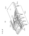
- Fig. 8 shows a semiconductor device described in Japanese Patent Laying-Open Gazette No. 7-250485 .
- the semiconductor device shown in Fig. 8 is a perspective view showing a module (Intelligent Power Module: hereinafter abbreviated as IPM) 80 storing power devices and an IC-ed control device controlling these power devices in a single package.
- IPM Intelligent Power Module
- the IPM 80 comprises a control IC 2100 which is an IC-ed control circuit and power chips 2200 which are power devices in an upper package OP10.
- the control IC 2100 and the power chips 2200 are electrically connected with control terminals TM10 and main circuit terminals TM20 respectively in the package.
- the upper package OP10 and a package base BP10 are formed by molding, and resin, such as epoxy resin, for example, is the main component thereof.
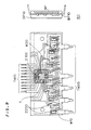
- Fig. 9 shows a plan perspective view and a sectional view in case of observing the IPM 80 from the side of the upper package OP10 (upper surface side).
- control IC 2100 is electrically connected with the control terminals TM10 through gold wires W20, and the power chips 2200 are electrically connected with the main circuit terminals TM20 through aluminum wires W10.
- the main circuit terminals TM20 have functions for serving not only as terminals but also as die pads for mounting the control IC 2100 and the power chips 2200.
- a heat sink HP is arranged on lower portions of the control terminals TM10 and the main circuit terminals TM20, to be in a structure of radiating heat generated by the power chips 2200 in a device operation through the heat sink HP.
- a fabrication process for the IPM 80 of such a structure is first adapted to prepare a lead frame which is one of elements forming the IPM 80, for die-bonding the control IC 2100 and the power chips 2200 to prescribed positions of this lead frame. The process is then adapted to connect the control IC 2100 and the control terminals TM10 with each other through the gold wires W20 and to connect the power chips 2200 and the main circuit terminals TM20 with each other through the aluminum wires W10, thereby completing packaging on the lead frame.
- the diameter of the gold wires W20 is about 30 ⁇ m
- the diameter of the aluminum wires W10 is about 300 ⁇ m.
- the IPM 80 is completed by performing transfer molding in a state mounting the aforementioned packaged lead frame on the heat sink HP.
- the transfer molding is a method of performing forming of resin by holding the packaged lead frame with upper and lower molds and press-fitting plastified (plastification) thermosetting resin (hereinafter referred to as mold resin) into cavities of these molds.
- mold resin press-fitting plastified (plastification) thermosetting resin
- the gold wires W20 are thinner than the aluminum wires W10 as described above, and hence deformation and breakage of the gold wires such as wire deformation in which the shape of the gold wires W20 is lost by press fitting of mold resin, a wire touch in which adjacent gold wires W20 come into contact with each other and wire disconnection in which the gold wires W20 are broken may take place.
- a method generally employed in order to prevent the aforementioned phenomena is a method of coating a region where gold wires are employed, i.e., a placed region of a control IC by employing resin such as polyimide, for example, in advance of transfer molding.
- resin such as polyimide
- a region X to which hatching is applied is the object region, when describing with reference to Fig. 9 .
- EP 0 420 267 relates to the technique of sealing semiconductor devices in resin.
- the present invention aims at soling the aforementioned problems, and providing a semiconductor device of high reliability by preventing deformation and breakage of gold wires without increasing the fabrication cost.
- the present invention provides a semiconductor device in accordance with independent claim 1; further a process for forming a semiconductor device is given in independent claim 3. Further preferred embodiments are given in the dependent claims.
- FIG. 1 An embodiment 1 of the semiconductor device according to the present invention is described while employing Fig. 1 showing a fabrication step for a module (Intelligent Power Module: hereinafter abbreviated as IPM) 100 storing power devices (power devices) and an IC-ed control unit (control device) in a single package (refer to Fig. 3 shown later).
- IPM Intelligent Power Module
- Fig. 1 is a diagram showing a state of placing a lead frame 10 forming the IPM 100 of Fig. 3 on a substantially rectangular cavity 22 of a molding die 20.
- the lead frame 10 has power device die pads 1 and control device die pads 2 extending from a tie bar 5 in plural respectively, and power devices PD are mounted on the power device die pads 1 while control devices CD are mounted on the control device die pads 2, and fixed by die bonding.
- the power device die pads 1 and the control device die pads 2 are arranged on single sides of the lead frame respectively. Namely, the power device die pads 1 are arranged/formed on a slightly lower side than the plane center, and the control device die pads 2 are arranged/formed on a slightly upper side than the plane center in Fig. 1 .
- the power devices PD are electrically connected with prescribed portions on the lead frame 10 through aluminum wires W1
- the control devices CD are electrically connected with prescribed portions on the lead frame 10 through gold wires W2, and packaging is completed.
- the semiconductor device is so structured that a region (first region) where the aluminum wires W1 are arranged and a region (second region) where the gold wires W2 are arranged do not mix with each other.
- the lead frame 10 is so position-controlled that the power device die pads 1 and the control device die pads 2 completely go in the cavity 22 and placed on the molding die 20.
- the molding die 20 is the so-called lower molding die of a transfer molding equipment for forming resin by holding a packaged lead frame with upper and lower molding dies and press-fitting plastified (plastification) thermosetting resin (hereinafter referred to as mold resin) into cavities of these molding dies, and the cavity 22 is a concave part which is formed in this lower molding die. While an upper molding die opposed to the molding die 20 exists, it is omitted in the figure.
- the region where the gold wires W2 are arranged may not be coated with resin such as polyimide for a reason described later, and hence such a structure is not shown in Fig. 1 .
- a single mold gate 21 (resin inlet port) is provided in the molding die 20, to intersect with a substantially central portion of one longer side of the cavity 22.
- the mold gate 21 is a groove for introducing mold resin into the cavity 22.
- This mold gate 21 is formed to be positioned on a side where the power device die pads 1 are arranged, i.e., a side where the power devices PD are arranged in a state placing the lead frame 10.
- the contour shape of the cavity 22 in plan view is in a shape incapable of placing the lead frame 10 in such a state that the arrangement side of the power devices PD and the arrangement side of the control devices CD are reversed. Therefore, it can be said that the molding die 20 shown in Fig. 1 is in such a structure that the mold gate 21 is provided on the power device side, and it can be said that the IPM 100 formed by the molding die 20 of such a structure is an IPM into which resin is injected from the power device side.
- FIG. 1 shows the structure of forming the mold gate 21 on the molding die 20 which is the lower mold for simplifying the illustration, the same can be provided on an upper molding die which is not illustrated, as a matter of course.
- the contour shape of the cavity 22 in plan view is properly modified, and it is in a structure that no concave part is provided on lower surfaces of the power device die pads 1 so that the mold resin does not infiltrate therein due to relation of heat radiation in reality.
- mold resin MR is in a short shot state, and the mold resin MR introduced from the mold gate 21 of Fig. 1 does not reach the region where the gold wires W2 are arranged. While those of about 30 ⁇ m in diameter are employed for the gold wires W2 at this point, those of about 300 ⁇ m in diameter are employed for the aluminum wires W1, whereby the same have sufficient strength against inflow pressure of the resin.
- the aluminum wires W1 are not deformed or broken even if the mold resin is injected at a relatively fast speed (first speed) until the mold resin MR reaches the region where the gold wires W2 are arranged, i.e., until a prescribed time (previously known by a test) elapses after injection start, whereby the productivity can be improved following improvement of the injection speed for the mold resin.
- a semiconductor device having high reliability can be obtained, while the region where the gold wires W2 are arranged may not be coated with resin such as polyimide dissimilarly to the IPM 80 described with reference to Fig. 9 , a step accompanying coating becomes unnecessary, fabrications steps are simplified, and the fabrication cost can be reduced.
- resin such as polyimide dissimilarly to the IPM 80 described with reference to Fig. 9
- the injection speed for the mold resin MR is set at 6 mm/sec. until reaching the region where the gold wires W2 are arranged and at about 0.3 mm/sec. thereafter, the productivity can be improved, while deformation and breakage of the gold wires W2 can be prevented.
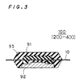
- Fig. 3 shows a sectional view illustrating the overall structure of the IPM 100.
- Fig. 3 is a sectional view of the substantially rectangular IPM 100 in a shorter side direction.
- the IPM 100 is formed by the first package 91 (including the lead frame 10) 91 formed in the transfer molding step described with reference to Fig. 1 , a heat sink 92 mounting this first package 91 and radiating heat generated by the power devices in a device operation to the exterior, and a second package 93 covering the first package 91 and the heat sink 92.
- traces of the mold gate 21 remain on an end surface of one longer side direction of the first package 91, i.e., on an end surface of the side where the power devices PD are arranged, and an injection direction of the mold resin, i.e., the arrangement side of the power devices PD on the IPM 100 can be clearly known.
- transfer molding of two times is performed for forming the first package 91 by performing transfer molding on the lead frame 10 and thereafter forming the second package 93 by performing transfer molding on the first package 91 and the heat sink 92 in the IPM 100.
- the device is in a structure capable of univocally settling the distances from the lower surfaces of the power device die pads 1 to the heat sink 92 by mounting the first package 91 on the heat sink 92.
- the distances from the lower surfaces of the power device die pads 1 of Fig. 1 to the heat sink 92 of Fig. 3 can be correctly maintained, and a semiconductor device excellent in insulation property and heat radiation property can be obtained.
- the lead frame 10 is formed by a metal plate having a uniform thickness
- the lead frame 10 of such a structure can be used since the same is in a structure excellent in heat radiation property as described above and hence deformation by heat or the like does not take place even if the thickness of the power device die pads 1 is equalized with that of the control device die pads 2.
- the injection speed for the mold resin there is no limitation for the injection speed for the mold resin, whereby the injection time may be short even if the same is of a large volume.
- the injection direction for the mold resin there is no limitation in particular in the injection direction for the mold resin either, while the injection direction for the mold resin is set in the same direction as that for the first package, in order to perform an efficient operation in consideration of transportation of the first package 91 and the like.
- the aforementioned overall structure of the IPM 100 is similar also in an IPM 200 to an IPM 400 described later, and redundant description is omitted.
- the mold gate is not restricted to a piece.
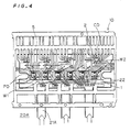
- Fig. 4 is a diagram illustrating a fabrication step for an IPM 200 according to the embodiment 2, and is a diagram showing a state of placing a lead frame 10 forming the IPM 200 on a substantially rectangular cavity 22 of a molding die 20A.
- Three mold gates 21A of the same groove width are provided substantially at regular intervals on the molding die 20A, to intersect with one longer side of the cavity 22.
- These mold gates 21A are formed to be positioned on a side where power device die pads 1 are arranged, i.e., a side where power devices PD are arranged in a state placing the lead frame 10.
- mold resin MR is in a short shot state, and the mold resin MR introduced from the three mold gates 21 does not reach a region where gold wires W2 are arranged.
- the mold resin MR is substantially homogeneously diffused in the cavity 22 in this state. This is because the mold resin MR is introduced from the three mold gates 21A, injection is well-balanced, and it comes to that the mold resin MR is so diffused that its forward end surface is substantially parallel to the longer side of the cavity 22.
- the mold resin MR is substantially homogeneously diffused in the cavity 22, whereby a prescribed time up to when the mold resin MR reaches the region where the gold wires W2 are arranged can be correctly known, and deformation and breakage of the gold wires W2 can be more reliably prevented.
- the forward end surface of the mold resin MR does not partially project, whereby occurrence of difference in a time up to reaching the region where the gold wires W2 are arranged is prevented in a projecting part and a part which is not so, and the prescribed time up to reaching the region where the gold wires W2 are arranged is uniformalized. Therefore, the timing for switching the injection speed for the mold resin can be correctly decided, and the gold wires W2 are prevented from being subjected to deformation and breakage by the mold resin whose injection speed is fast.
- the number of the mold gates 21A is not restricted to three, but properly decided in consideration of the size of the cavity and the like.
- the groove widths of the mold gates may not be identical.
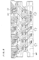
- Fig. 6 is a diagram illustrating a fabrication step for an IPM 300 related to such a modification, and is a diagram showing a state of placing a lead frame 10 forming the IPM 300 on a substantially rectangular cavity 22 of a molding die 20B.
- Three mold gates 211B, 212B and 213B whose groove widths are different are provided on the molding die 20B, to intersect with one longer side of the cavity 22. Referring to Fig. 6 , the groove widths increase in order of the mold gates 211B, 212B and 213B.
- These mold gates 211B, 212B and 213B are formed to be positioned on a side where power device die pads 1 are arranged, i.e., a side where power devices PD are arranged in a state placing the lead frame 10.
- mold resin is heated/softened in a transfer pot, extruded by a transfer plunger, and injected into a cavity through mold gates.
- a transfer plunger extruded by a transfer plunger
- the distances from the transfer pot to the plurality of mold gates are not identical.
- the mold resin is supplied with relatively strong pressure to a mold gate which is on a position close to the transfer pot in this case, pressure of the mold resin supplied to a mold gate on a position far from the transfer pot weakens.
- the groove widths of the mold gates 211B, 212B and 213B differ from each other, whereby the injection amounts of the mold resin per unit time can be made identical, and the mold resin can be homogeneously diffused in the cavity.
- the groove widths of the mold gates 211B, 212B and 213B are so decided that injection amounts per unit time become identical, in consideration of pressure of the mold resin supplied from the transfer pot.
- mold resin can be homogeneously diffused with a single mold gate.
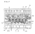
- Fig. 7 is a diagram illustrating a fabrication step for an IPM 400 according to the embodiment 3, and is a diagram showing a state of placing a lead frame 10 forming the IPM 400 on a substantially rectangular cavity 22 of a molding die 20C.
- the molding die 20C is, to intersect with one longer side of the cavity 22, provided with a single mold gate 21C whose groove width is extremely wide as compared with this longer side.
- This mold gate 21C is formed to be positioned on a side where power device die pads 1 are arranged, i.e., a side where power devices PD are arranged in a state placing the lead frame 10.
- mold resin MR introduced from the mold gate 21C is substantially homogeneously diffused in the cavity 22. This state is similar to the state described with reference to Fig. 5 , and hence illustration is omitted.
- the mold resin MR is substantially homogeneously diffused in the cavity 22, whereby such an effect that a prescribed time up to when the mold resin MR reaches a region where gold wires W2 are arranged can be correctly known and deformation and breakage of the gold wires W2 can be further reliably prevented is similar to that of the IPM 200 described as the embodiment 2.
- resin whose viscosity is relatively low may be used in case of injecting the same at a relatively fast speed (first speed), and resin whose viscosity is relatively high may be used in case of injecting the same at a relatively slow speed (second speed).
- a first mold resin layer is formed with the resin whose viscosity is relatively low on the region (first region) where the aluminum wires W1 and a second mold resin layer is formed with the resin whose viscosity is relatively high on the region (second region) where the gold wires W2 are arranged.
- first and second mold resin layers are not completely integrated due to difference in solidification time or the like but can be distinguished as first and second mold resin layers as described above in a mold resin layer formed with the mold resin MR injected at a relatively fast speed (first speed) and a mold resin layer formed with the mold resin MR injected at a relatively slow speed (second speed).
Applications Claiming Priority (1)
| Application Number | Priority Date | Filing Date | Title |
|---|---|---|---|
| PCT/JP1996/003496 WO1998024122A1 (fr) | 1996-11-28 | 1996-11-28 | Dispositif a semi-conducteur |
Publications (3)
| Publication Number | Publication Date |
|---|---|
| EP0910121A1 EP0910121A1 (en) | 1999-04-21 |
| EP0910121A4 EP0910121A4 (en) | 2000-12-06 |
| EP0910121B1 true EP0910121B1 (en) | 2009-01-07 |
Family
ID=14154168
Family Applications (1)
| Application Number | Title | Priority Date | Filing Date |
|---|---|---|---|
| EP96940147A Expired - Lifetime EP0910121B1 (en) | 1996-11-28 | 1996-11-28 | Semiconductor device |
Country Status (5)
| Country | Link |
|---|---|
| US (1) | US6002166A (ja) |
| EP (1) | EP0910121B1 (ja) |
| JP (1) | JP3338063B2 (ja) |
| DE (1) | DE69637809D1 (ja) |
| WO (1) | WO1998024122A1 (ja) |
Families Citing this family (25)
| Publication number | Priority date | Publication date | Assignee | Title |
|---|---|---|---|---|
| DE19805785C1 (de) * | 1998-02-12 | 1999-06-17 | Siemens Ag | Leistungshalbleiter-Modul mit thermischer Laststromsicherung |
| JP4256502B2 (ja) * | 1998-11-12 | 2009-04-22 | 新光電気工業株式会社 | 半導体装置用リードフレームと半導体装置 |
| JP3813775B2 (ja) * | 1999-11-05 | 2006-08-23 | ローム株式会社 | マルチチップモジュール |
| JP4037589B2 (ja) * | 2000-03-07 | 2008-01-23 | 三菱電機株式会社 | 樹脂封止形電力用半導体装置 |
| KR100442847B1 (ko) | 2001-09-17 | 2004-08-02 | 페어차일드코리아반도체 주식회사 | 3차원 구조를 갖는 전력 반도체 모듈 및 그 제조방법 |
| US6900527B1 (en) * | 2001-09-19 | 2005-05-31 | Amkor Technology, Inc. | Lead-frame method and assembly for interconnecting circuits within a circuit module |
| JP2003124437A (ja) * | 2001-10-19 | 2003-04-25 | Mitsubishi Electric Corp | 半導体装置 |
| US6617679B2 (en) * | 2002-02-08 | 2003-09-09 | Advanced Energy Industries, Inc. | Semiconductor package for multiple high power transistors |
| JP3828036B2 (ja) * | 2002-03-28 | 2006-09-27 | 三菱電機株式会社 | 樹脂モールド型デバイスの製造方法及び製造装置 |
| US7145223B2 (en) * | 2002-05-22 | 2006-12-05 | Matsushita Electric Industrial Co., Ltd. | Semiconductor device |
| DE102005038755B4 (de) * | 2005-08-17 | 2016-03-10 | Robert Bosch Gmbh | Mikromechanisches Bauelement |
| KR101255334B1 (ko) * | 2006-05-08 | 2013-04-16 | 페어차일드코리아반도체 주식회사 | 저 열저항 파워 모듈 및 그 제조방법 |
| KR101194041B1 (ko) * | 2006-12-07 | 2012-10-24 | 페어차일드코리아반도체 주식회사 | 고전력 반도체 패키지 |
| KR101391924B1 (ko) * | 2007-01-05 | 2014-05-07 | 페어차일드코리아반도체 주식회사 | 반도체 패키지 |
| KR101489325B1 (ko) * | 2007-03-12 | 2015-02-06 | 페어차일드코리아반도체 주식회사 | 플립-칩 방식의 적층형 파워 모듈 및 그 파워 모듈의제조방법 |
| JP2011049442A (ja) * | 2009-08-28 | 2011-03-10 | Asahi Kasei Electronics Co Ltd | 半導体装置及びその製造方法 |
| JP5565372B2 (ja) * | 2011-04-22 | 2014-08-06 | 株式会社デンソー | 電子装置の製造方法 |
| JP2013070026A (ja) | 2011-09-08 | 2013-04-18 | Rohm Co Ltd | 半導体装置、半導体装置の製造方法、半導体装置の実装構造、およびパワー用半導体装置 |
| JP5278529B2 (ja) * | 2011-12-29 | 2013-09-04 | 三菱電機株式会社 | 半導体モジュール |
| DE102012222679A1 (de) * | 2012-12-10 | 2014-06-12 | Robert Bosch Gmbh | Verfahren zur Herstellung eines Schaltmoduls und eines zugehörigen Gittermoduls sowie ein zugehöriges Gittermodul und korrespondierende elektronische Baugruppe |
| JP6065581B2 (ja) * | 2012-12-26 | 2017-01-25 | サンケン電気株式会社 | パワー半導体モジュールおよびその製造方法 |
| DE112014007140B4 (de) * | 2014-11-07 | 2024-05-02 | Mitsubishi Electric Corporation | Leistungshalbleiteranordnung und Verfahren zum Herstellen derselben |
| JP2022064768A (ja) | 2020-10-14 | 2022-04-26 | 富士電機株式会社 | 半導体装置の製造方法及び半導体装置 |
| CN115939119B (zh) * | 2022-11-17 | 2023-11-03 | 海信家电集团股份有限公司 | 功率模块和电子设备 |
| CN115799238A (zh) * | 2022-11-17 | 2023-03-14 | 海信家电集团股份有限公司 | 功率模块和电子设备 |
Family Cites Families (18)
| Publication number | Priority date | Publication date | Assignee | Title |
|---|---|---|---|---|
| JPS56122157A (en) * | 1980-02-29 | 1981-09-25 | Nec Corp | Semiconductor device |
| JPS6063122A (ja) * | 1983-09-16 | 1985-04-11 | Michio Osada | 半導体素子の樹脂封入成形方法及びその金型装置 |
| JPH0680748B2 (ja) * | 1986-03-31 | 1994-10-12 | 株式会社東芝 | 樹脂封止型半導体装置 |
| DE3684184D1 (de) * | 1985-06-20 | 1992-04-16 | Toshiba Kawasaki Kk | Verkapselte halbleiteranordnung. |
| JPS6398631A (ja) * | 1986-10-16 | 1988-04-30 | Nec Home Electronics Ltd | カプセル型液晶表示装置 |
| JPH0713984B2 (ja) * | 1989-06-28 | 1995-02-15 | シャープ株式会社 | 半導体装置の製造方法 |
| JP2588283B2 (ja) * | 1989-09-29 | 1997-03-05 | 株式会社東芝 | 樹脂封止型半導体装置 |
| JPH03188661A (ja) * | 1989-12-18 | 1991-08-16 | Toshiba Corp | 樹脂封止型半導体装置 |
| JPH0529539A (ja) * | 1991-07-17 | 1993-02-05 | Matsushita Electric Works Ltd | マルチチツプモジユール |
| JPH0682699B2 (ja) * | 1992-04-01 | 1994-10-19 | 道男 長田 | 半導体素子の樹脂封止成形方法 |
| FR2690274B1 (fr) * | 1992-04-15 | 1997-08-22 | Motorola Semiconducteurs | Boitier pour dispositif a semiconducteur et procede de formation de boitier pour dispositif a semiconducteur. |
| JP2708320B2 (ja) * | 1992-04-17 | 1998-02-04 | 三菱電機株式会社 | マルチチップ型半導体装置及びその製造方法 |
| JP2701712B2 (ja) * | 1993-11-11 | 1998-01-21 | 日本電気株式会社 | 半導体装置 |
| JP3325697B2 (ja) * | 1994-01-20 | 2002-09-17 | 三菱電機株式会社 | パワーデバイスの制御装置およびモータの駆動制御装置 |
| JP2601228B2 (ja) * | 1994-11-18 | 1997-04-16 | サンケン電気株式会社 | 樹脂封止型回路装置の製造方法 |
| JP3429921B2 (ja) * | 1995-10-26 | 2003-07-28 | 三菱電機株式会社 | 半導体装置 |
| US5767567A (en) * | 1996-09-10 | 1998-06-16 | Magemos Corporation | Design of device layout for integration with power mosfet packaging to achieve better lead wire connections and lower on resistance |
| US5872403A (en) * | 1997-01-02 | 1999-02-16 | Lucent Technologies, Inc. | Package for a power semiconductor die and power supply employing the same |
-
1996
- 1996-11-28 DE DE69637809T patent/DE69637809D1/de not_active Expired - Lifetime
- 1996-11-28 US US09/117,171 patent/US6002166A/en not_active Expired - Lifetime
- 1996-11-28 EP EP96940147A patent/EP0910121B1/en not_active Expired - Lifetime
- 1996-11-28 JP JP52236698A patent/JP3338063B2/ja not_active Expired - Lifetime
- 1996-11-28 WO PCT/JP1996/003496 patent/WO1998024122A1/ja active Application Filing
Also Published As
| Publication number | Publication date |
|---|---|
| US6002166A (en) | 1999-12-14 |
| EP0910121A1 (en) | 1999-04-21 |
| JP3338063B2 (ja) | 2002-10-28 |
| WO1998024122A1 (fr) | 1998-06-04 |
| EP0910121A4 (en) | 2000-12-06 |
| DE69637809D1 (de) | 2009-02-26 |
Similar Documents
| Publication | Publication Date | Title |
|---|---|---|
| EP0910121B1 (en) | Semiconductor device | |
| US5527740A (en) | Manufacturing dual sided wire bonded integrated circuit chip packages using offset wire bonds and support block cavities | |
| US8497158B2 (en) | Leadframe strip and mold apparatus for an electronic component and method of encapsulating an electronic component | |
| US6558980B2 (en) | Plastic molded type semiconductor device and fabrication process thereof | |
| US5789280A (en) | Leadframe having secured outer leads, semiconductor device using the leadframe and method of making them | |
| EP0409196B1 (en) | Plastic molded type semiconductor device | |
| US5837567A (en) | Lead frame and semiconductor device | |
| JPH1126489A (ja) | ゲートスロットを有するサブストレートならびに半導体パッケージ成形用の金型および成形方法 | |
| KR200309906Y1 (ko) | 반도체 패키지 제조용 리드프레임 | |
| US6277225B1 (en) | Stress reduction feature for LOC lead frame | |
| US5623163A (en) | Leadframe for semiconductor devices | |
| EP0657922B1 (en) | A packaged semiconductor device and method of its manufacture | |
| KR100591718B1 (ko) | 수지-밀봉형 반도체 장치 | |
| US5672550A (en) | Method of encapsulating semiconductor devices using a lead frame with resin tablets arranged on lead frame | |
| JP2983105B2 (ja) | 半導体装置およびその製法 | |
| US5811132A (en) | Mold for semiconductor packages | |
| JP3609821B1 (ja) | 半導体装置封止用金型およびそれを用いた半導体装置封止方法 | |
| JP3813680B2 (ja) | 半導体装置の製造方法 | |
| KR100531423B1 (ko) | 반도체 패키지 제조용 리드프레임 및 이에 적용되는 몰드다이, 그리고 이를 이용한 패키지 제조장치. | |
| KR100258876B1 (ko) | 반도체 시험용 패키지의 제조방법 | |
| JPH08330343A (ja) | 電子部品の樹脂封止装置およびこれを用いた樹脂封止方法 | |
| JPH09129661A (ja) | 成形装置および成形方法 | |
| JPH08156009A (ja) | 樹脂モールド装置 | |
| JP2003045905A (ja) | 樹脂封止方法及び樹脂封止装置 | |
| JPH11111744A (ja) | 半導体装置の製造方法 |
Legal Events
| Date | Code | Title | Description |
|---|---|---|---|
| PUAI | Public reference made under article 153(3) epc to a published international application that has entered the european phase |
Free format text: ORIGINAL CODE: 0009012 |
|
| 17P | Request for examination filed |
Effective date: 19980728 |
|
| AK | Designated contracting states |
Kind code of ref document: A1 Designated state(s): DE FR GB |
|
| A4 | Supplementary search report drawn up and despatched |
Effective date: 20001025 |
|
| AK | Designated contracting states |
Kind code of ref document: A4 Designated state(s): DE FR GB |
|
| RIC1 | Information provided on ipc code assigned before grant |
Free format text: 7H 01L 21/56 A, 7H 01L 23/29 B, 7H 01L 25/04 B, 7H 01L 23/495 B |
|
| RAP1 | Party data changed (applicant data changed or rights of an application transferred) |
Owner name: MITSUBISHI DENKI KABUSHIKI KAISHA |
|
| GRAP | Despatch of communication of intention to grant a patent |
Free format text: ORIGINAL CODE: EPIDOSNIGR1 |
|
| GRAS | Grant fee paid |
Free format text: ORIGINAL CODE: EPIDOSNIGR3 |
|
| GRAA | (expected) grant |
Free format text: ORIGINAL CODE: 0009210 |
|
| AK | Designated contracting states |
Kind code of ref document: B1 Designated state(s): DE FR GB |
|
| REG | Reference to a national code |
Ref country code: GB Ref legal event code: FG4D |
|
| REF | Corresponds to: |
Ref document number: 69637809 Country of ref document: DE Date of ref document: 20090226 Kind code of ref document: P |
|
| PLBE | No opposition filed within time limit |
Free format text: ORIGINAL CODE: 0009261 |
|
| STAA | Information on the status of an ep patent application or granted ep patent |
Free format text: STATUS: NO OPPOSITION FILED WITHIN TIME LIMIT |
|
| 26N | No opposition filed |
Effective date: 20091008 |
|
| REG | Reference to a national code |
Ref country code: GB Ref legal event code: 746 Effective date: 20110513 |
|
| REG | Reference to a national code |
Ref country code: DE Ref legal event code: R084 Ref document number: 69637809 Country of ref document: DE Effective date: 20110506 Ref country code: DE Ref legal event code: R084 Ref document number: 69637809 Country of ref document: DE Effective date: 20110627 |
|
| PGFP | Annual fee paid to national office [announced via postgrant information from national office to epo] |
Ref country code: FR Payment date: 20121130 Year of fee payment: 17 |
|
| PGFP | Annual fee paid to national office [announced via postgrant information from national office to epo] |
Ref country code: GB Payment date: 20121128 Year of fee payment: 17 |
|
| GBPC | Gb: european patent ceased through non-payment of renewal fee |
Effective date: 20131128 |
|
| REG | Reference to a national code |
Ref country code: FR Ref legal event code: ST Effective date: 20140731 |
|
| PG25 | Lapsed in a contracting state [announced via postgrant information from national office to epo] |
Ref country code: GB Free format text: LAPSE BECAUSE OF NON-PAYMENT OF DUE FEES Effective date: 20131128 Ref country code: FR Free format text: LAPSE BECAUSE OF NON-PAYMENT OF DUE FEES Effective date: 20131202 |
|
| PGFP | Annual fee paid to national office [announced via postgrant information from national office to epo] |
Ref country code: DE Payment date: 20151125 Year of fee payment: 20 |
|
| REG | Reference to a national code |
Ref country code: DE Ref legal event code: R071 Ref document number: 69637809 Country of ref document: DE |