EP0817282A2 - Halbleiterbauelement - Google Patents
Halbleiterbauelement Download PDFInfo
- Publication number
- EP0817282A2 EP0817282A2 EP97304379A EP97304379A EP0817282A2 EP 0817282 A2 EP0817282 A2 EP 0817282A2 EP 97304379 A EP97304379 A EP 97304379A EP 97304379 A EP97304379 A EP 97304379A EP 0817282 A2 EP0817282 A2 EP 0817282A2
- Authority
- EP
- European Patent Office
- Prior art keywords
- single crystal
- nitride
- substrate
- aluminum nitride
- iii
- Prior art date
- Legal status (The legal status is an assumption and is not a legal conclusion. Google has not performed a legal analysis and makes no representation as to the accuracy of the status listed.)
- Granted
Links
- 239000004065 semiconductor Substances 0.000 title claims abstract description 61
- 239000013078 crystal Substances 0.000 claims abstract description 260
- 239000000758 substrate Substances 0.000 claims abstract description 158
- PMHQVHHXPFUNSP-UHFFFAOYSA-M copper(1+);methylsulfanylmethane;bromide Chemical compound Br[Cu].CSC PMHQVHHXPFUNSP-UHFFFAOYSA-M 0.000 claims abstract description 91
- 150000004767 nitrides Chemical class 0.000 claims abstract description 88
- 229910002601 GaN Inorganic materials 0.000 claims abstract description 54
- JMASRVWKEDWRBT-UHFFFAOYSA-N Gallium nitride Chemical compound [Ga]#N JMASRVWKEDWRBT-UHFFFAOYSA-N 0.000 claims abstract description 52
- 239000000956 alloy Substances 0.000 claims abstract description 13
- 229910045601 alloy Inorganic materials 0.000 claims abstract description 13
- PZNSFCLAULLKQX-UHFFFAOYSA-N Boron nitride Chemical compound N#B PZNSFCLAULLKQX-UHFFFAOYSA-N 0.000 claims abstract description 10
- 229910052582 BN Inorganic materials 0.000 claims abstract description 9
- NWAIGJYBQQYSPW-UHFFFAOYSA-N azanylidyneindigane Chemical compound [In]#N NWAIGJYBQQYSPW-UHFFFAOYSA-N 0.000 claims abstract description 8
- 238000003776 cleavage reaction Methods 0.000 claims description 20
- 230000007017 scission Effects 0.000 claims description 20
- 229910052723 transition metal Inorganic materials 0.000 claims description 10
- 150000003624 transition metals Chemical class 0.000 claims description 10
- RTAQQCXQSZGOHL-UHFFFAOYSA-N Titanium Chemical compound [Ti] RTAQQCXQSZGOHL-UHFFFAOYSA-N 0.000 claims description 9
- 229910052719 titanium Inorganic materials 0.000 claims description 9
- 239000010936 titanium Substances 0.000 claims description 9
- 150000001875 compounds Chemical class 0.000 claims description 4
- 238000002441 X-ray diffraction Methods 0.000 claims description 3
- 230000010355 oscillation Effects 0.000 abstract description 7
- 239000010408 film Substances 0.000 description 136
- 230000015572 biosynthetic process Effects 0.000 description 26
- 238000000034 method Methods 0.000 description 18
- 239000007789 gas Substances 0.000 description 16
- 239000000463 material Substances 0.000 description 16
- 229910052594 sapphire Inorganic materials 0.000 description 14
- 239000010980 sapphire Substances 0.000 description 14
- 238000010438 heat treatment Methods 0.000 description 13
- QGZKDVFQNNGYKY-UHFFFAOYSA-N Ammonia Chemical compound N QGZKDVFQNNGYKY-UHFFFAOYSA-N 0.000 description 10
- 239000000843 powder Substances 0.000 description 10
- XCZXGTMEAKBVPV-UHFFFAOYSA-N trimethylgallium Chemical compound C[Ga](C)C XCZXGTMEAKBVPV-UHFFFAOYSA-N 0.000 description 10
- BLRPTPMANUNPDV-UHFFFAOYSA-N Silane Chemical compound [SiH4] BLRPTPMANUNPDV-UHFFFAOYSA-N 0.000 description 9
- UFHFLCQGNIYNRP-UHFFFAOYSA-N Hydrogen Chemical compound [H][H] UFHFLCQGNIYNRP-UHFFFAOYSA-N 0.000 description 8
- GWEVSGVZZGPLCZ-UHFFFAOYSA-N Titan oxide Chemical compound O=[Ti]=O GWEVSGVZZGPLCZ-UHFFFAOYSA-N 0.000 description 8
- QVGXLLKOCUKJST-UHFFFAOYSA-N atomic oxygen Chemical compound [O] QVGXLLKOCUKJST-UHFFFAOYSA-N 0.000 description 8
- 230000017525 heat dissipation Effects 0.000 description 8
- 239000011812 mixed powder Substances 0.000 description 8
- 229910052760 oxygen Inorganic materials 0.000 description 8
- 239000001301 oxygen Substances 0.000 description 8
- IJGRMHOSHXDMSA-UHFFFAOYSA-N Atomic nitrogen Chemical compound N#N IJGRMHOSHXDMSA-UHFFFAOYSA-N 0.000 description 7
- 239000012159 carrier gas Substances 0.000 description 7
- 230000006866 deterioration Effects 0.000 description 6
- -1 gallium nitride compound Chemical class 0.000 description 6
- 229910052984 zinc sulfide Inorganic materials 0.000 description 6
- OKTJSMMVPCPJKN-UHFFFAOYSA-N Carbon Chemical compound [C] OKTJSMMVPCPJKN-UHFFFAOYSA-N 0.000 description 5
- 229910026161 MgAl2O4 Inorganic materials 0.000 description 5
- 238000006243 chemical reaction Methods 0.000 description 5
- 229910052710 silicon Inorganic materials 0.000 description 5
- 239000010703 silicon Substances 0.000 description 5
- 229910052596 spinel Inorganic materials 0.000 description 5
- 238000004544 sputter deposition Methods 0.000 description 5
- LFQSCWFLJHTTHZ-UHFFFAOYSA-N Ethanol Chemical compound CCO LFQSCWFLJHTTHZ-UHFFFAOYSA-N 0.000 description 4
- 230000000052 comparative effect Effects 0.000 description 4
- 229910003460 diamond Inorganic materials 0.000 description 4
- 239000010432 diamond Substances 0.000 description 4
- 238000001312 dry etching Methods 0.000 description 4
- 229910052739 hydrogen Inorganic materials 0.000 description 4
- 239000001257 hydrogen Substances 0.000 description 4
- 239000012535 impurity Substances 0.000 description 4
- 239000000203 mixture Substances 0.000 description 4
- 238000003786 synthesis reaction Methods 0.000 description 4
- IBEFSUTVZWZJEL-UHFFFAOYSA-N trimethylindium Chemical compound C[In](C)C IBEFSUTVZWZJEL-UHFFFAOYSA-N 0.000 description 4
- 229910052782 aluminium Inorganic materials 0.000 description 3
- XAGFODPZIPBFFR-UHFFFAOYSA-N aluminium Chemical compound [Al] XAGFODPZIPBFFR-UHFFFAOYSA-N 0.000 description 3
- 229910052799 carbon Inorganic materials 0.000 description 3
- 238000000295 emission spectrum Methods 0.000 description 3
- 229910052757 nitrogen Inorganic materials 0.000 description 3
- 239000012299 nitrogen atmosphere Substances 0.000 description 3
- 238000002128 reflection high energy electron diffraction Methods 0.000 description 3
- JLTRXTDYQLMHGR-UHFFFAOYSA-N trimethylaluminium Chemical compound C[Al](C)C JLTRXTDYQLMHGR-UHFFFAOYSA-N 0.000 description 3
- PIGFYZPCRLYGLF-UHFFFAOYSA-N Aluminum nitride Chemical compound [Al]#N PIGFYZPCRLYGLF-UHFFFAOYSA-N 0.000 description 2
- GYHNNYVSQQEPJS-UHFFFAOYSA-N Gallium Chemical compound [Ga] GYHNNYVSQQEPJS-UHFFFAOYSA-N 0.000 description 2
- 230000008859 change Effects 0.000 description 2
- 230000007547 defect Effects 0.000 description 2
- 230000002542 deteriorative effect Effects 0.000 description 2
- 238000009792 diffusion process Methods 0.000 description 2
- 229910002804 graphite Inorganic materials 0.000 description 2
- 239000010439 graphite Substances 0.000 description 2
- 230000006698 induction Effects 0.000 description 2
- 239000012212 insulator Substances 0.000 description 2
- 238000004519 manufacturing process Methods 0.000 description 2
- 238000002156 mixing Methods 0.000 description 2
- 229910003465 moissanite Inorganic materials 0.000 description 2
- 238000001451 molecular beam epitaxy Methods 0.000 description 2
- 230000003287 optical effect Effects 0.000 description 2
- 238000011056 performance test Methods 0.000 description 2
- 230000008569 process Effects 0.000 description 2
- 238000009877 rendering Methods 0.000 description 2
- 229910010271 silicon carbide Inorganic materials 0.000 description 2
- 239000012808 vapor phase Substances 0.000 description 2
- IPWKGIFRRBGCJO-IMJSIDKUSA-N Ala-Ser Chemical compound C[C@H]([NH3+])C(=O)N[C@@H](CO)C([O-])=O IPWKGIFRRBGCJO-IMJSIDKUSA-N 0.000 description 1
- 229910001218 Gallium arsenide Inorganic materials 0.000 description 1
- FYYHWMGAXLPEAU-UHFFFAOYSA-N Magnesium Chemical compound [Mg] FYYHWMGAXLPEAU-UHFFFAOYSA-N 0.000 description 1
- ZLMJMSJWJFRBEC-UHFFFAOYSA-N Potassium Chemical compound [K] ZLMJMSJWJFRBEC-UHFFFAOYSA-N 0.000 description 1
- BUGBHKTXTAQXES-UHFFFAOYSA-N Selenium Chemical compound [Se] BUGBHKTXTAQXES-UHFFFAOYSA-N 0.000 description 1
- XUIMIQQOPSSXEZ-UHFFFAOYSA-N Silicon Chemical compound [Si] XUIMIQQOPSSXEZ-UHFFFAOYSA-N 0.000 description 1
- NINIDFKCEFEMDL-UHFFFAOYSA-N Sulfur Chemical compound [S] NINIDFKCEFEMDL-UHFFFAOYSA-N 0.000 description 1
- ATJFFYVFTNAWJD-UHFFFAOYSA-N Tin Chemical compound [Sn] ATJFFYVFTNAWJD-UHFFFAOYSA-N 0.000 description 1
- HCHKCACWOHOZIP-UHFFFAOYSA-N Zinc Chemical compound [Zn] HCHKCACWOHOZIP-UHFFFAOYSA-N 0.000 description 1
- 238000013459 approach Methods 0.000 description 1
- 230000008901 benefit Effects 0.000 description 1
- 229910052790 beryllium Inorganic materials 0.000 description 1
- ATBAMAFKBVZNFJ-UHFFFAOYSA-N beryllium atom Chemical compound [Be] ATBAMAFKBVZNFJ-UHFFFAOYSA-N 0.000 description 1
- 239000013590 bulk material Substances 0.000 description 1
- 238000005229 chemical vapour deposition Methods 0.000 description 1
- 238000000748 compression moulding Methods 0.000 description 1
- 238000010276 construction Methods 0.000 description 1
- 238000007796 conventional method Methods 0.000 description 1
- 238000000354 decomposition reaction Methods 0.000 description 1
- 229910001873 dinitrogen Inorganic materials 0.000 description 1
- 230000000694 effects Effects 0.000 description 1
- 230000007613 environmental effect Effects 0.000 description 1
- 238000005530 etching Methods 0.000 description 1
- 229910052733 gallium Inorganic materials 0.000 description 1
- 230000006872 improvement Effects 0.000 description 1
- 238000003475 lamination Methods 0.000 description 1
- 229910052749 magnesium Inorganic materials 0.000 description 1
- 239000011777 magnesium Substances 0.000 description 1
- 230000008018 melting Effects 0.000 description 1
- 238000002844 melting Methods 0.000 description 1
- 229910052751 metal Inorganic materials 0.000 description 1
- 239000002184 metal Substances 0.000 description 1
- 239000003960 organic solvent Substances 0.000 description 1
- 239000011591 potassium Substances 0.000 description 1
- 229910052700 potassium Inorganic materials 0.000 description 1
- 238000002360 preparation method Methods 0.000 description 1
- 230000002265 prevention Effects 0.000 description 1
- 230000000644 propagated effect Effects 0.000 description 1
- 230000005855 radiation Effects 0.000 description 1
- 230000009467 reduction Effects 0.000 description 1
- 229910052711 selenium Inorganic materials 0.000 description 1
- 239000011669 selenium Substances 0.000 description 1
- 238000004611 spectroscopical analysis Methods 0.000 description 1
- 238000000859 sublimation Methods 0.000 description 1
- 230000008022 sublimation Effects 0.000 description 1
- 229910052717 sulfur Inorganic materials 0.000 description 1
- 239000011593 sulfur Substances 0.000 description 1
- 229910052714 tellurium Inorganic materials 0.000 description 1
- PORWMNRCUJJQNO-UHFFFAOYSA-N tellurium atom Chemical compound [Te] PORWMNRCUJJQNO-UHFFFAOYSA-N 0.000 description 1
- 239000010409 thin film Substances 0.000 description 1
- 229910052718 tin Inorganic materials 0.000 description 1
- 239000011135 tin Substances 0.000 description 1
- 230000007704 transition Effects 0.000 description 1
- GETQZCLCWQTVFV-UHFFFAOYSA-N trimethylamine Chemical compound CN(C)C GETQZCLCWQTVFV-UHFFFAOYSA-N 0.000 description 1
- 238000001771 vacuum deposition Methods 0.000 description 1
- 230000008016 vaporization Effects 0.000 description 1
- 229910052725 zinc Inorganic materials 0.000 description 1
- 239000011701 zinc Substances 0.000 description 1
Images


Classifications
-
- H—ELECTRICITY
- H01—ELECTRIC ELEMENTS
- H01S—DEVICES USING THE PROCESS OF LIGHT AMPLIFICATION BY STIMULATED EMISSION OF RADIATION [LASER] TO AMPLIFY OR GENERATE LIGHT; DEVICES USING STIMULATED EMISSION OF ELECTROMAGNETIC RADIATION IN WAVE RANGES OTHER THAN OPTICAL
- H01S5/00—Semiconductor lasers
- H01S5/30—Structure or shape of the active region; Materials used for the active region
- H01S5/32—Structure or shape of the active region; Materials used for the active region comprising PN junctions, e.g. hetero- or double- heterostructures
- H01S5/323—Structure or shape of the active region; Materials used for the active region comprising PN junctions, e.g. hetero- or double- heterostructures in AIIIBV compounds, e.g. AlGaAs-laser, InP-based laser
- H01S5/32308—Structure or shape of the active region; Materials used for the active region comprising PN junctions, e.g. hetero- or double- heterostructures in AIIIBV compounds, e.g. AlGaAs-laser, InP-based laser emitting light at a wavelength less than 900 nm
- H01S5/32341—Structure or shape of the active region; Materials used for the active region comprising PN junctions, e.g. hetero- or double- heterostructures in AIIIBV compounds, e.g. AlGaAs-laser, InP-based laser emitting light at a wavelength less than 900 nm blue laser based on GaN or GaP
-
- H—ELECTRICITY
- H01—ELECTRIC ELEMENTS
- H01L—SEMICONDUCTOR DEVICES NOT COVERED BY CLASS H10
- H01L33/00—Semiconductor devices having potential barriers specially adapted for light emission; Processes or apparatus specially adapted for the manufacture or treatment thereof or of parts thereof; Details thereof
- H01L33/005—Processes
- H01L33/0062—Processes for devices with an active region comprising only III-V compounds
- H01L33/0075—Processes for devices with an active region comprising only III-V compounds comprising nitride compounds
Definitions
- the present invention relates to semiconductor devices using a III-group element nitride (hereinafter, III-V nitride)for use in, for example, a reader of a high-density optical disk, including short-wavelength light emitting devices, such as a light emitting diode or a laser diode, light-receiving devices such as a photodiode, high-temperature semiconductor devices which can operate even in a high-temperature environment, and high-speed operation semiconductor devices.
- III-V nitride III-group element nitride
- a III-V nitride having a wurtzite structure is a direct transition type semiconductor having a wide forbidden band and, hence, has attracted attention as a material for a short-wavelength light emitting device or a light-receiving device and, further, a high-temperature semiconductor device and a high-speed semiconductor device.
- the III-V nitrides having the above wurtzite structure include gallium nitride (GaN), aluminum nitride (AlN), boron nitride (BN), indium nitride (InN), and single-crystalline alloys of these nitrides.
- the forbidden band width can be varied by varying the type of the material and the composition of the single-crystalline alloy.
- gallium nitride and single-crystalline alloys thereof have been actively studied as the material of light emitting devices.
- blue and bluish green LEDs (light emitting diodes) using a gallium nitride compound semiconductor have been put to practical use, and, in the next stage, practical use of short-wavelength LDs (laser diodes) in a reader for a high-density optical disk is expected in the art.
- a single crystal film of a semiconductor should be grown on a substrate of a single crystal of the same crystal structure.
- III-V nitrides a single crystal having a size large enough to be used as the substrate could have not been synthesized, and, hence, hetero-epitaxial growth wherein a single crystal film of a III-V nitride is grown on a dissimilar substrate has been used in the art.
- Substrates known to be usable for the hetero-epitaxial growth include the (0001) plane (plane C) and the (11-20) plane (plane A) of a single crystal of sapphire, the (111) plane of a single crystal of silicon, the (0001) plane of a single crystal of 6H-SiC, and the (111) plane of a single crystal of MgAl 2 O 4 .
- the single crystal substrate of sapphire among these substrates permits the growth of a single crystal film of a gallium nitride compound semiconductor having good crystallinity through a low-temperature growth buffer layer and, in addition, is relatively inexpensive. Therefore, it is most commonly used in blue and bluish green LEDs utilizing the above gallium nitride compound semiconductor.
- LDs those in an infrared region using a GaAs compound semiconductor or an InP compound semiconductor have been put to practical use, but blue-emitting LDs using a III-V nitride are still under study and there are some reports thereon. Examples of such reports include Jpn. J. Appl. Phys., Vol. 35 (1996), pp. L74-L76, Jpn. J. Appl. Phys., Vol. 35 (1996), pp. L217-L220, and Appl. Phys. Lett., Vol. 68, No. 15 (1996), pp. 2105-2107. All the LDs cited in these reports are of a pulse oscillation type.
- III-V nitrides have not been yet put to practical use, although application of III-V nitrides as a light emitting device has been partly realized. This also is because many defects such as dislocation are included in the single crystal film of a III-V nitride. The dislocation is propagated under high temperature conditions, leading to remarkably deteriorated performance, which results in a shortened service life. Further, the dislocation lowers the mobility of the carrier unfavorably, making it impossible to realize high-speed operation.
- heat dissipation should be improved because light emitting devices, particularly LDs, have a high calorific value at the time of light emission, high-speed semiconductor devices have a high calorific value at the time of high-speed operation, and, further, high-temperature semiconductor devices also need the prevention of deterioration thereof.
- substrates having high heat conductivity is desired.
- all of substrates made of sapphire, silicon, MgAl 2 O 4 , and the like, which permit the crystal growth of a necessary single crystal film have low heat conductivity. Therefore, in devices where high output and temperature stability are required, these substrates are used in the form bonded to a heat sink material. Jpn. J. Appl.
- the substrate in this example is a thin-film single crystal substrate comprising a single crystal substrate of diamond bearing at least one single crystal layer formed of at least one material selected from among gallium nitride, indium nitride, aluminum nitride and the like.
- This example is aimed at providing a substrate having high heat conductivity, low coefficient of thermal expansion, and excellent heat resistance and environmental resistance.
- This single crystal substrate of diamond also is unsatisfactory in matching in lattice constant and coefficient of thermal expansion with the single crystal of a III-V nitride.
- substrate materials such as sapphire, silicon, SiC, and MgAl 2 O 4 , which have hitherto been used for the growth of a single crystal film of a III-V nitride are unsatisfactory in matching in lattice constant and coefficient of thermal expansion with the III-V nitride.
- the heat conductivity is so low that, for use in light emitting devices, the substrate should be bonded to a heat sink. Further, in this case, since sapphire is not electrically conductive, it is difficult to handle an electrode in the bonding to the heat sink.
- an object of the present invention is to grow a single crystal film of a III-V nitride having good crystallinity on a substrate having good matching in lattice constant and coefficient of thermal expansion with a III-V nitride, particularly on a substrate having a cleavage surface and good thermal conductivity and capable of offering a relatively large single crystal, thereby providing semiconductor devices using a III-V nitride, such as short-wavelength light emitting devices capable of conducting continuous oscillation, light receiving devices, high-temperature semiconductor devices, and high-speed semiconductor devices.
- the above object can be attained by a semiconductor device comprising a single crystal substrate of aluminum nitride and a single crystal film of at least one III-V nitride provided on the substrate, wherein the at least one III-V nitride of the single crystal film is selected from the group consisting of gallium nitride, aluminum nitride, boron nitride, indium nitride, and single-crystalline alloys of these compounds.
- the single crystal film may be formed onto the aluminum nitride single crystal substrate either directly or through a low-temperature growth buffer layer consisting of at least one III-V nitride selected from the group consisting of gallium nitride, aluminum nitride, boron nitride, indium nitride, and single-crystalline alloys of these compounds.
- Semiconductor devices referred to in the present invention include light emitting devices, light receiving devices, high-temperature semiconductor devices, and high-speed semiconductor devices, and examples of the light emitting devices include light emitting diodes (LEDs) and laser diodes (LDs).
- LEDs light emitting diodes
- LDs laser diodes
- the mirror facet for a laser cavity can be formed by the cleavage of a single crystal substrate of aluminum nitride and a single crystal film of a III-V nitride.
- the (10-10) or (11-20) plane of a single crystal film of a III-V nitride is utilized as the cleavage surface, and, for this purpose, the (0001) plane of a single crystal of aluminum nitride is used as the substrate.
- the (0001) plane of the single crystal film of a III-V nitride may be utilized as the cleavage surface, and, for this purpose, the (10-10) or (11-20) plane of the single crystal of aluminum nitride may be advantageously used as the substrate.
- the present invention using a single crystal of aluminum nitride as the substrate, it is also possible to construct a semiconductor device in such a manner that the provision of a low-temperature growth buffer layer of a III-V nitride, which has been necessary for growing a single crystal film of a III-V nitride having excellent crystallinity and smooth film surface, is omitted and a single crystal film of a III-V nitride film is formed directly on a single crystal substrate of aluminum nitride.
- Fig. 1 is a schematic cross-sectional view of a principal part of the semiconductor device according to the present invention.
- Fig. 2 is a schematic cross-sectional view of a heating furnace used in the preparation of the single crystal substrate of aluminum nitride in Example 1.
- Fig. 3 is a schematic cross-sectional view of the structure of the light emitting diode prepared in Example 1.
- Fig. 4 is a schematic cross-sectional view of the structure of the laser diode prepared in Example 2.
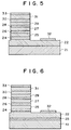
- Fig. 5 is a schematic cross-sectional view of the structure of the laser diode prepared in Example 3.
- Fig. 6 is a schematic cross-sectional view of the structure of the laser diode prepared in Comparative Example 1.
- Fig. 7 is a schematic cross-sectional view of the structure of the diode prepared in Example 7.
- Fig. 8 is a schematic cross-sectional view of the structure of the diode prepared in Comparative Example 2.
- a III-V nitride is grown on a single crystal substrate of aluminum nitride (AlN), which has lattice constant and coefficient of thermal expansion close to those of the III-V nitride and good thermal conductivity and can be produced in a relatively large single crystal form, to form a single crystal film having excellent crystallinity, thereby realizing semiconductor devices such as light emitting devices suitable for light emission at short wavelengths.
- AlN aluminum nitride
- the single crystal of a III-V nitride does not naturally occur and should be artificially synthesized, and single crystals of boron nitride, gallium nitride, and aluminum nitride have hitherto been artificially synthesized.
- a single crystal of aluminum nitride can be stably and inexpensively synthesized in a relatively large size, rendering this single crystal suitable for use as a substrate in the formation of a semiconductor device.
- the present inventors have proposed in Japanese Patent Application No. 141236/1996 a process for preparing a single crystal of a nitride having a larger size and a higher quality.
- This process comprises mixing a powder of a nitride, such as AlN, with a powder of an oxide which can be reacted with the nitride under heating to decompose and vaporize the nitride, and heating the mixed powders in a nitrogen atmosphere optionally containing hydrogen and/or carbon at a temperature below the sublimation temperature or melting temperature of the nitride to permit the nitride powder to be reacted with the oxide powder, thereby decomposing and vaporizing the nitride powder and permitting the decomposed and vaporized component to be grown from a vapor phase on the substrate to provide a nitride such as AlN.
- a single crystal of aluminum nitride having a size sufficient for practical use as a bulk material specifically a single crystal of aluminum nitride of not less than 10 mm in both length and width and not less than 300 ⁇ m in thickness
- This large and high-quality single crystal of aluminum nitride is best suited as a substrate for the semiconductor device according to the present invention.
- the use of an oxide of a group IVa or Va element, especially a TiO 2 powder, as the oxide to be mixed with the AlN powder is preferred.
- a high-quality single crystal of aluminum nitride wherein not less than 90% by mole of a total content of components other than nitrogen is accounted for by Al and the oxygen content is not more than 500 ppm, is particularly preferred as the substrate for the semiconductor device according to the present invention.
- the contents of the components constituting the aluminum nitride single crystal substrate are indicated based on a total content of the components other than nitrogen, unless otherwise specified.
- the crystallinity of the above single crystal of aluminum nitride is preferably such that the half value width of a rocking curve obtained by X-ray diffractometry is 1.5 min or less.
- the thickness of aluminum nitride as the substrate is preferably not less than 300 ⁇ m. When the thickness is less than 300 ⁇ m, the crystallinity is likely to be lowered.
- the single crystal of aluminum nitride contains a transition metal in an amount of 10 ppb to not more than 0.1% by mole with the transition metal being preferably titanium.
- the transition metal is likely to bond to oxygen deteriorating the performance of the semiconductor device and serves to capture the oxygen impurities contained in a minute amount in the single crystal to reduce the diffusion of oxygen from the single crystal into the semiconductor device, preventing the deterioration of the performance of the semiconductor device.
- the content of the transition metal is less than 10 ppb, the above effect cannot be attained.
- it exceeds 0.1% by mole the transition metal and its nitride and oxide and the like are precipitated as an undesired material, deteriorating the crystallinity of the single crystal of aluminum nitride.
- the crystallinity of the single crystal film formed on the single crystal substrate becomes better as the lattice constant and the coefficient of thermal expansion of the single crystal substrate approach those of the single crystal film.
- Aluminum nitride used as the substrate in the present invention is a III-V nitride in itself. Therefore, the lattice constant and the coefficient of thermal expansion thereof are closer to those of the III-V nitride constituting the single crystal film than those of sapphire, silicon, SiC, and MgAl 2 O 4 .
- the III-V nitride film formed on the single crystal substrate of aluminum nitride has good crystallinity, and the light emitting device of the present invention produced by using this single crystal film has better properties than light emitting devices having conventional structures. Therefore, unlike the prior art wherein the provision of a low-temperature growth buffer layer is necessary and indispensable for forming a single crystal film of a III-V nitride having good crystallinity on a dissimilar substrate, the present invention does not necessarily require the provision of the buffer layer.
- LD should have a mirror facet for a laser cavity in its structure.
- a high evenness is required of the mirror facet, and hence the creation of the mirror facet by cleavage is preferred.
- the single crystal film and the single crystal substrate are matched in crystal orientation and are coincident with each other in cleavage surface. Therefore, unlike conventional sapphire substrates and the like, the mirror facet can be easily formed by the cleavage of the single crystal substrate and the single crystal film.
- the use of a substrate of a (0001), (10-10), or (11-20) plane as the single crystal substrate of aluminum nitride is preferred.
- the formation of a mirror facet perpendicular to the substrate surface by utilizing the (10-10) or (11-20) plane as the cleavage surface facilitates the formation of the device.
- the formation of a mirror facet perpendicular to the substrate surface by utilizing the (0001) or (1-210) plane as the cleavage surface in the case of the substrate of the (10-10) plane and utilizing the (0001) or (1-100) plane as the cleavage surface in the case of the substrate of the (11-20) plane facilitates the formation of the device.
- the cleavage surface is inclined relative to the substrate, rendering the handling at the time of formation of the device difficult.
- the substrate of a (10-10) plane or the substrate of a (11-20) plane is preferred.
- the reason for this is as follows.
- the cleavage surface is present for every 30° rotation, the cleavage surface is not always flat, making it difficult to form an even mirror facet, whereas in the case of the substrate of a (10-10) plane and the substrate of a (11-20) plane, the cleavage surface is present for every 90° rotation, and a flat mirror facet can be relatively easily formed.
- the roughness (in terms of Ra specified by Japanese Industrial Standard) of the surface on which a single crystal film of a III-V nitride is to be formed is preferably not more than 0.1 ⁇ m from the viewpoint of growing a singe crystal film of a III-V nitride having excellent crystallinity and surface smoothness of the film on the surface of the substrate.
- the single crystal film of a III-V nitride grown on the single crystal substrate of aluminum nitride is a film of a III-V nitride having a wurtzite structure
- III-V nitrides include GaN, AlN, BN, InN, and single-crystalline alloys thereof, such as Al x Ga (1-x) N, In x Ga (1-x) N, B x Ga (1-x) N, B x A1 (1-x) N, In x Al (1-x) N, and B x In (1-x) N.
- the single-crystalline alloys in addition to the above three-component single-crystalline alloys, four-component and other multi-component single-crystalline alloys may be used.
- Single crystal films of these III-V nitrides may be grown on the single crystal substrate of aluminum nitride by any conventional method for forming a single crystal film on a substrate, and examples of such methods include MBE (Molecular Beam Epitaxy method), MOCVD (Metal Organic Chemical Vapor Deposition method), sputtering, and vacuum deposition. In these methods, heating the substrate to a high temperature is necessary for the growth of a single crystal film.
- the substrate temperature at which the single crystal film can be grown varies depending upon the kind of the film to be grown and the film forming method. In the case of a single crystal of a III-V nitride, the substrate temperature is preferably between 500°C and 1300°C.
- a single crystal film of a III-V nitride can be grown on the substrate of aluminum nitride without interposition of any low-temperature growth buffer layer.
- the formation of a low-temperature growth buffer layer of a III-V nitride on the substrate followed by the formation of a single crystal film on the buffer layer is preferred from the viewpoint of growing a single crystal film of a III-V nitride having excellent crystallinity and smoothness of the film surface.
- a III-V nitride having a wurtzite structure may be used as the buffer layer.
- the nitride has matched lattice.
- the material of the buffer layer is not limited to the material identical with the material of the single crystal film grown on the buffer layer.
- the low-temperature growth buffer layer may be formed by the same method as described above in connection with the formation of the single crystal film of a III-V nitride. In this case, however, the substrate temperature should be below that for the formation of the single crystal film to grow an amorphous or polycrystalline film.
- the substrate temperature for the formation of the low-temperature buffer layer varies depending upon the kind of the film to be grown and the film forming method. In general, however, it is between 20°C and 900°C. In this connection, it should be noted that the low-temperature growth buffer layer is amorphous or polycrystalline immediately after the formation thereof and, when the substrate temperature is raised to form a single crystal film on the buffer layer, is in many cases converted to a single crystal type.
- the electric conductivity is controlled by adding impurities.
- impurities at least one element selected from among silicon, tin, oxygen, sulfur, selenium, tellurium and the like may be added to impart n-type conductivity, while at least one element selected from among zinc, beryllium, magnesium, potassium and the like may be added to impart p-type conductivity.
- the electric conductivity may be controlled by adding impurities.
- a single crystal film 2 of a III-V nitride on a single crystal substrate 1 of aluminum nitride followed by the lamination of a single crystal film of a III-V nitride, with the band gap being varied by varying the material or the composition of the single-crystalline alloy, on the surface of the single crystal film 2 and the provision of predetermined electrodes can provide semiconductor devices of the present invention such as light emitting diodes and laser diodes.
- a single crystal of aluminum nitride as a substrate was prepared by the following procedure.
- An AlN powder having a purity of 99% and a TiO 2 powder having a purity of 99% were mixed together in a molar ratio of TiO 2 to AlN powder of 0.75.
- the mixture was then subjected to ultrasonic mixing in ethanol and then dried to remove ethanol, thereby preparing a mixed powder.
- a c-plane-cut, ⁇ -type SiC single crystal plate having a size of 10 mm square was provided as a substrate for crystal growth.
- the mixed powder and the single crystal plate of SiC were placed in a heating furnace as shown in Fig. 2.
- a heating furnace 3 is provided with an induction heating coil 4 and a heat insulator muffle 5, and a vessel-like lidded graphite crucible 6 is provided on the inside of the heat insulator muffle 5, while a non-lidded BN crucible 7 is placed on the inside of the graphite crucible 6.
- An inlet 8a and an outlet 8b for an atmospheric gas are provided at the top of the heating furnace 3.
- the mixed powder 9 after compression molding was placed within the BN crucible 7 in the heating furnace 3, and the single crystal plate of SiC as a substrate 10 was set above so as to face the mixed powder 9.
- the interior of the heating furnace 3 was once evacuated, and a nitrogen gas was introduced through the inlet 8a into the furnace 3 to bring the pressure within the furnace 3 to 1 atm (760 Torr). Then, the temperature around the mixed powder 9 was heated by induction heating to 1800°C, a temperature below the decomposition temperature of AlN (2200°C), while the temperature around the substrate 10 was heated to 1700°C by controlling the heating section. The system was held in this state for 24 hr. In this case, the components of the vapor phase within the heating furnace 3 were analyzed by spectroscopy. As a result, it was found that the partial pressure of oxygen was 0.05 Torr with the ratio of the partial pressure of carbon (Pr) to the partial pressure of oxygen (Po), Pr/Po, being 2.0.
- the single crystal of aluminum nitride thus obtained was ground to give an even surface and washed with an organic solvent, and the (0001) plane thereof was used as a substrate to form a light emitting diode (LED) with an active layer of In 0.1 Ga 0.9 N.
- LED light emitting diode
- the structure of this light emitting diode is shown in Fig. 3.
- a light emitting diode (LED) with an active layer of In 0.1 Ga 0.9 N was prepared by using the above aluminum nitride substrate 11, forming a single crystal film 12 of n-type GaN on the surface of the aluminum nitride substrate 11 through a low-temperature growth buffer layer 13 of n-type GaN, forming a single crystal film 14 of n-type In 0.1 Ga 0.9 N and a single crystal film 15 of p-type GaN thereon in that order, and forming electrodes 16 and 17.
- the single crystal film of each III-V nitride was grown by the MOCVD under atmospheric pressure according to the following procedure.
- the low-temperature growth buffer layer 13 of n-type GaN was formed as follows. Hydrogen was introduced as a carrier gas into the reaction chamber at a flow rate of 10 liter/min together with NH 3 , trimethylgallium, and SiH 4 (diluted with H 2 to a concentration of 10 ppm) as the source gases respectively at flow rates of 4.0 liter/min, 30 ⁇ mol/min, and 4 nmol/min, and the system was kept in this state at a substrate temperature of 500°C for one min.
- a low-temperature buffer layer 13 of n-type GaN was grown with a thickness of 25 nm on the single crystal substrate 11 of aluminum nitride. Thereafter, the temperature of the substrate was raised to 1000°C while keeping the above gas introduction conditions, and a single crystal film 12 of n-type GaN was grown in this state on the low-temperature buffer layer 13 to a thickness of 4 ⁇ m over a period of 60 min.
- the temperature of the substrate was brought to 800°C, and a hydrogen gas was introduced as a carrier gas into the reaction chamber at a flow rate of 10 liter/min together with NH 3 , trimethylindium, trimethylgallium, and SiH 4 (diluted with H 2 to a concentration of 10 ppm) as the source gases, respectively, at flow rates of 4.0 liter/min, 24 ⁇ mol/min, 2 ⁇ mol/min, and 1 nmol/min.
- a single crystal film 14 of n-type In 0.1 Ga 0.9 N was grown on the single crystal film 12 of n-type GaN to a thickness of 20 nm over a period of 7 min.
- the temperature of the substrate was again raised to 1000°C, and a single crystal film 15 of p-type GaN was grown on the single crystal film 14 of n-type In 0.1 Ga 0.9 N to a thickness of 0.8 ⁇ m over a period of 15 min.
- the gases used were the same as those used in the growth of the single crystal film 12 of n-type GaN, except that biscyclopentadiethylmagnesium was used instead of SiH 4 at a flow rate of 3.6 ⁇ mol/min.
- the whole substrate with the single crystal films grown thereon was annealed in a nitrogen atmosphere at 700°C. Thereafter, each of the single crystal nitride films was partially processed by reactive dry etching to expose part of the single crystal layer 12 of n-type GaN on the surface. Finally, aluminum electrodes 16 and 17 were formed by sputtering respectively on the single crystal film 15 of p-type GaN as the uppermost layer and the exposed single crystal film 12 of n-type GaN to prepare the LED.
- each of the single crystal film 12 of n-type GaN, the single crystal film 14 of n-type In 0.1 Ga 0.9 N, and the single crystal film 15 of p-type GaN was a single crystal film having a wurtzite structure, and that the (0001) plane of the single crystal film was grown in parallel with the (0001) plane of the single crystal substrate 11 of aluminum nitride.
- the LED thus obtained was evaluated for the properties thereof at room temperature. As a result, a blue light emission having a peak wavelength at 440 nm was confirmed. Continuous light emission of the LED for 1 hr neither caused such a large temperature rise of the device as will influence the performance of the device nor resulted in a deterioration in the properties such as brightness.
- the (0001) plane of the same single crystal of aluminum nitride as used in Example 1 was used as a substrate to prepare a laser diode (LD), with a structure shown in Fig. 4, having a quantum well structure 27 of In 0.2 Ga 0.8 N/In 0.05 Ga 0.95 N as an active layer.
- LD laser diode
- a low-temperature growth buffer layer 23 of n-type GaN was formed on the surface of the substrate 21 of aluminum nitride, and subsequently a single crystal film 22 of n-type GaN, a single crystal film 24 of n-type In 0.1 Ga 0.9 N, a single crystal film 25 of n-type Al 0.15 Ga 0.85 N, a single crystal film 26 of n-type GaN, a quantum-well structure 27 of In 0.2 Ga 0.8 N/In 0.05 Ga 0.95 N, a single crystal film 28 of p-type Al 0.2 Ga 0.8 N, a single crystal film 29 of p-type GaN, a single crystal film 30 of p-type Al 0.15 Ga 0.85 N, and a single crystal film 31 of p-type GaN were formed thereon in that order, followed by the formation of electrodes 32 and 33 to prepare the LD.
- the single crystal film of each of the above III-V nitrides was grown by the MOCVD under atmospheric pressure according to the following procedure.
- the low-temperature growth buffer layer 23 of n-type GaN was grown on the single crystal substrate 21 of aluminum nitride at a substrate temperature of 500°C.
- hydrogen was introduced as a carrier gas into the reaction chamber at a flow rate of 10 liter/min together with NH 3 , trimethylgallium, and SiH 4 (diluted with H 2 to a concentration of 10 ppm) as the source gases, respectively, at flow rates of 4.0 liter/min, 30 ⁇ mol/min, and 4 nmol/min to grow the low-temperature growth buffer layer 23 of n-type GaN to a thickness of 25 nm.
- the temperature of the substrate was raised to 1000°C while keeping the above gas introduction conditions, and a single crystal film 22 of n-type GaN was grown in this state on the low-temperature buffer layer 23 of n-type GaN to a thickness of 4 ⁇ m over a period of 60 min.
- Hydrogen gas was then introduced as a carrier gas into the reaction chamber at a flow rate of 10 liter/min together with NH 3 , trimethylindium, trimethylgallium, and SiH 4 (diluted with H 2 to a concentration of 10 ppm) as the source gases, respectively, at flow rates of 4.0 liter/min, 24 ⁇ mol/min, 2 ⁇ mol/min, and 1 nmol/min to grow the single crystal film 24 of n-type In 0.1 Ga 0.9 N on the single crystal film 22 of n-type GaN to a thickness of 100 nm over a period of 35 min.
- the temperature of the substrate was again raised to 1000°C, and a single crystal film 25 of n-type Al 0.15 Ga 0.85 N was grown.
- NH 3 , trimethylaluminum, trimethylgallium, and SiH 4 (diluted with H 2 to a concentration of 10 ppm) were used as the source gases, respectively, at flow rates of 4.0 liter/min, 6 ⁇ mol/min, 24 ⁇ mol/min, and 4 nmol/min to grow the single crystal film of n-type Al 0.15 Ga 0.85 N to a thickness of 400 nm over a period of 5 min.
- a single crystal film 26 of n-type GaN was then grown on the single crystal film 25 of n-type Al 0.15 Ga 0.85 N.
- the gases used were the same as those used in the growth of the single crystal film 22 of n-type GaN, and the single crystal film 26 of n-type GaN was grown to a thickness of 100 nm over a period of 2 min.
- In 0.2 Ga 0.8 N and In 0.05 Ga 0.95 N were laminated on the single crystal film 26 of n-type GaN in respective thicknesses of 2.5 nm and 5.0 nm to form a quantum well structure 27 of 26 periods.
- a hydrogen gas was used as a carrier gas at a flow rate of 10 liter/min together with NH 3 , trimethylgallium, and trimethylindium as the source gases, respectively, at flow rates of 4.0 liter/min, 1 ⁇ mol/min, and 24 ⁇ mol/min.
- a hydrogen gas was used as a carrier gas at a flow rate of 10 liter/min together with NH 3 , trimethylgallium, and trimethylindium as the source gases, respectively, at flow rates of 4.0 liter/min, 1 ⁇ mol/min, and 1.2 ⁇ mol/min.
- a single crystal film 28 of p-type Al 0.2 Ga 0.8 N was grown.
- NH 3 , trimethylaluminum, trimethylgallium, and biscyclopentadiethylmagnesium were used as the source gases, respectively, at flow rates of 4.0 liter/min, 10 ⁇ mol/min, 24 ⁇ mol/min, and 3.6 ⁇ mol/min to grow the single crystal film 28 of p-type Al 0.2 Ga 0.8 N to a thickness of 200 nm over a period of 4 min.
- a single crystal film 29 of p-type GaN was grown on the single crystal film 28 of p-type Al 0.2 Ga 0.8 N.
- the gases used for growth were the same as those used in the growth of the single crystal film 22 of n-type GaN, except that biscyclopentadiethylmagnesium was used instead of SiH 4 (diluted with H 2 to a concentration of 10 ppm) at a flow rate of 3.6 ⁇ mol/min.
- the single crystal film 29 was grown to a thickness of 100 nm.
- a single crystal film 30 of p-type Al 0.15 Ga 0.85 N was grown on the single crystal film 29 of p-type GaN.
- the source gases used for the growth were the same as those used in the growth of the single crystal film 25 of n-type Al 0.15 Ga 0.85 N, except that biscyclopentadiethylmagnesium was used instead of SiH 4 (diluted with H 2 to a concentration of 10 ppm) at a flow rate of 3.6 ⁇ mol/min.
- the single crystal film 30 was grown to a thickness of 400 nm over a period of 8 min.
- a single crystal film 31 of p-type GaN was grown thereon to a thickness of 500 nm in the same manner as in the formation of the single crystal film 29 of p-type GaN.
- each of the single crystal nitride films was partially processed by reactive dry etching to expose part of the lower single crystal layer 22 of n-type GaN to the surface.
- the (10-10) plane of the single crystal substrate 21 of aluminum nitride was cleaved to form alaser cavity.
- Aluminum electrodes 32 and 33 were then formed by sputtering respectively on the single crystal film 31 of p-type GaN as the uppermost layer and the exposed single crystal film 22 of n-type GaN to the prepare the LD.
- each of the layers was a single crystal film having a wurtzite structure, and the (0001) plane of the single crystal film was grown in parallel with the (0001) plane of the single crystal substrate 21 of aluminum nitride.
- the LED thus obtained was evaluated for the properties thereof at room temperature. As a result, the emission of laser beams having a peak wavelength at 420 nm and a half value width of 0.9 nm was confirmed. Continuous light emission of the LED for 1 hr neither caused such a large temperature rise of the device as will influence the performance of the device nor resulted in a deterioration in the properties such as brightness.
- An LD having a structure shown in Fig. 5 was prepared in the same manner as in Example 2, except that the low-temperature growth buffer layer 23 shown in Fig. 4 was not formed.
- the LD shown in Fig. 5 has the same structure as that shown in Fig. 4 in Example 2, except that the low-temperature growth buffer layer 23 is absent.
- this LD having the structure shown in Fig. 5 were evaluated at room temperature. As a result, the emission of laser beams having a peak wavelength at 420 nm and a half value width of 1.0 nm was confirmed. Continuous light emission of the LED for 1 hr neither caused such a large temperature rise of the device as will influence the performance of the device nor resulted in a deterioration in the properties such as brightness. These results show that there is no significant difference in practical performance of the LD between the provision of no low-temperature growth buffer layer and the provision of the low-temperature growth buffer layer in Example 2.
- an LD was formed in the same manner as in Example 2, except that a sapphire single crystal substrate 41 constituted of the (0001) plane face of a sapphire single crystal was used and the laser cavity was formed by dry etching.
- the LD shown in Fig. 6 has the same structure as that shown in Fig. 4 in Example 2, except that these LDs are different from each other in the material of the substrate and the method for forming the laser cavity.
- the LD thus obtained was evaluated for the properties thereof at room temperature. As a result, the emission of laser beams having a peak wavelength at 420 nm and a half value width of 1.8 nm was confirmed. However, continuous light emission of the LD for 10 min resulted in distinctly lowered luminance.
- the (10-10) plane of a single crystal of aluminum nitride was synthesized in the same manner as in Example 1, except that the (10-10) plane of 6H-SiC was used as the single crystal substrate of SiC in the synthesis of the single crystal of aluminum nitride as the substrate.
- the LD shown in Fig. 4 was prepared in the same manner as in Example 2, except that this (10-10) plane of the single crystal of aluminum nitride was used as the substrate and the (0001) plane was cleaved.
- the LD thus obtained was evaluated for the properties thereof at room temperature.
- the emission of laser beams having a peak wavelength at 420 nm and a half value width of 0.6 nm was confirmed.
- an LD having a narrower half value width in the emission spectrum can be formed by using the (10-10) plane as the single crystal substrate of aluminum nitride and constructing a laser cavity by the cleavage of the (0001) plane and the use of the (0001) plane in the formation of the laser cavity is preferred.
- the (0001) planes of single crystals of aluminum nitride were synthesized in the same manner as in Example 1, except that, in the synthesis of the single crystal of aluminum nitride as the substrate, the (0001) plane of 6H-SiC was used as the single crystal substrate of SiC and the time for the growth of the single crystals of aluminum nitride was 50 min and 1 hr.
- the LDs each having a structure shown in Fig. 4 were prepared in the same manner as in Example 2, except that the (0001) plane of each of the single crystals of aluminum nitride different from each other in thickness was used as the substrate.
- the LDs thus obtained were evaluated for the properties thereof at room temperature.
- the emission of laser beams each having a peak wavelength at 420 nm and having respective half value widths of 1.6 nm and 1.5 nm was confirmed. After light emission for 24 hr, the half-value widths were measured again and found to be 1.8 nm and 1.5 nm, respectively.
- the (0001) planes of single crystals of aluminum nitride were synthesized in the same manner as in Example 1, except that, in the synthesis of the single crystal of aluminum nitride as the substrate, the molar ratio of TiO 2 to AlN in the mixed powder was changed to 0.001, 0.2, and 10, that the (0001) plane of 6H-SiC was used as the single crystal substrate of SiC, and that the temperature around the mixed powder was 1900°C.
- the titanium contents of the single crystals thus obtained were respectively 8 ppb, 0.06% by mole, and 0.15% by mole of a total content of the components other than nitrogen.
- LDs each having a structure shown in Fig. 4 were prepared in the same manner as in Example 2, except that the (0001) plane of each of the single crystals of aluminum nitride different from each other in titanium content was used as the substrate.
- the LDs thus obtained were evaluated for the properties thereof at room temperature.
- the emission of laser beams each having a peak wavelength at 420 nm and having respective half value widths of 0.8 nm, 1.0 nm, and 1.9 nm was confirmed. After light emission for 24 hr, the half value widths were measured again and found to be 1.5 nm, 1.0 nm, and 1.9 nm, respectively.
- a p-n junction diode of Al 0.5 Ga 0.5 N having a structure shown in Fig. 7 was formed using, as a substrate, the (0001) plane of the same single crystal of aluminum nitride as used in Example 1. Specifically, as shown in Fig. 7, a single crystal film 34 of n-type Al 0.5 Ga 0.5 N was formed on the surface of the single crystal substrate 21 of aluminum nitride, and a single crystal film 35 of p-type Al 0.5 Ga 0.5 N was formed thereon, followed by provision of electrodes 36 and 37 to prepare a diode.
- the single crystal film of each of the above III-V nitrides was grown by the MOCVD under atmospheric pressure according to the following procedure.
- the single crystal film 34 of n-type Al 0.5 Ga 0.5 N was grown on the single crystal substrate 21 of aluminum nitride at a substrate temperature of 1000°C.
- hydrogen was introduced as a carrier gas into the reaction chamber at a flow rate of 10 liter/min together with NH 3 , trimethylaluminum, trimethylgallium, and SiH 4 (diluted with H 2 to a concentration of 10 ppm) as the source gases, respectively, at flow rates of 4.0 liter/min, 10 ⁇ mol/min, 16 ⁇ mol/min, and 4 nmol/min to grow the single crystal film 34 of n-type Al 0.5 Ga 0.5 N to a thickness of 300 nm over a period of 3 min.
- a single crystal film 35 of p-type Al 0.5 Ga 0.5 N was grown while keeping the substrate temperature at 1000°C.
- NH 3 , trimethylammonium, trimethylgallium, and biscyclopentadiethylmagnesium were used as the source gasses at respective flow rates of 4.0 liter/min, 10 ⁇ mol/min, 15 ⁇ mol/min, and 3.6 nmol/min to grow the single crystal film 35 of p-type Al 0.5 Ga 0.5 N to a thickness of 320 nm over a period of 4 min.
- each of the single crystal films 34 and 35 was partially processed by reactive dry etching to expose part of the lower single crystal film 34 of n-type Al 0.5 Ga 0.5 N on the surface. Thereafter, titanium electrodes 36 and 37 were formed by sputtering respectively on the exposed single crystal film 34 of n-type Al 0.5 Ga 0.5 N and the single crystal film 35 of p-type Al 0.5 Ga 0.5 N as the uppermost layer by sputtering to prepare a diode.
- the electric characteristics of the diode thus obtained were evaluated. As a result, it was found that the diode has good rectification characteristics at room temperature and functions as a diode. Further, the temperature was raised to 200°C, and the same performance test was carried out. As a result, rectification characteristics were confirmed, indicating that the diode functions as a diode even at a high temperature.
- a diode was formed in the same manner as in Example 7, except that, as shown in Fig. 8, a single crystal substrate 41 constituted of the (0001) plane of a sapphire single crystal was used. Specifically, the diode shown in Fig. 8 has the same structure as the diode shown in Fig. 7 in Example 7, except that these diodes are different from each other in the material of the substrate.
- the electric characteristics of the diode thus obtained were evaluated. As a result, it was found that the diode has rectification characteristics at room temperature and functions as a diode. Further, the temperature was raised to 200°C, and the same performance test was carried out. As a result, no rectification characteristics could be confirmed.
- the use of a large single crystal substrate of aluminum nitride which is matched in lattice constant and coefficient of thermal expansion with a III-V nitride and has a cleavage surface and good heat dissipation permits a single crystal film of a III-V nitride having good crystallinity to be grown on the substrate, thus making it possible to provide semiconductor devices using a III-V nitride, for example, short-wavelength light emitting devices capable of conducting continuous oscillation, light receiving devices, high-temperature semiconductor devices, and high-speed semiconductor devices.
- the present invention can eliminate the need to provide any low-temperature growth buffer layer which has been required in the art.
- the invention provides semiconductor devices having heat dissipation good enough to eliminate the need to mount any heat sink, thus realizing light emitting devices such as light emitting diodes and laser diodes particularly using a III-V nitride. In the case of a laser diode, this enables a laser cavity to be prepared by taking advantage of cleavage of the substrate.
Landscapes
- Physics & Mathematics (AREA)
- Engineering & Computer Science (AREA)
- Condensed Matter Physics & Semiconductors (AREA)
- Microelectronics & Electronic Packaging (AREA)
- Power Engineering (AREA)
- Computer Hardware Design (AREA)
- Manufacturing & Machinery (AREA)
- General Physics & Mathematics (AREA)
- Electromagnetism (AREA)
- Optics & Photonics (AREA)
- Led Devices (AREA)
- Semiconductor Lasers (AREA)
- Crystals, And After-Treatments Of Crystals (AREA)
Applications Claiming Priority (4)
| Application Number | Priority Date | Filing Date | Title |
|---|---|---|---|
| JP16397496 | 1996-06-25 | ||
| JP163974/96 | 1996-06-25 | ||
| JP119515/97 | 1997-05-09 | ||
| JP11951597A JP3644191B2 (ja) | 1996-06-25 | 1997-05-09 | 半導体素子 |
Publications (3)
| Publication Number | Publication Date |
|---|---|
| EP0817282A2 true EP0817282A2 (de) | 1998-01-07 |
| EP0817282A3 EP0817282A3 (de) | 1998-10-14 |
| EP0817282B1 EP0817282B1 (de) | 2007-08-15 |
Family
ID=26457232
Family Applications (1)
| Application Number | Title | Priority Date | Filing Date |
|---|---|---|---|
| EP97304379A Expired - Lifetime EP0817282B1 (de) | 1996-06-25 | 1997-06-23 | Halbleiterbauelement |
Country Status (4)
| Country | Link |
|---|---|
| US (1) | US5909036A (de) |
| EP (1) | EP0817282B1 (de) |
| JP (1) | JP3644191B2 (de) |
| DE (1) | DE69738008T2 (de) |
Cited By (5)
| Publication number | Priority date | Publication date | Assignee | Title |
|---|---|---|---|---|
| DE19953839A1 (de) * | 1999-11-09 | 2001-05-10 | Paul Drude Inst Fuer Festkoerp | Hocheffiziente UV-Emitter auf Nitridhalbleiterbasis |
| EP1142024A1 (de) * | 1998-11-16 | 2001-10-10 | Emcore Corporation | Iii-nitrid-quantentopfstrukturen mit indiumreichen clustern und deren herstellungsverfahren |
| EP1166411A1 (de) * | 1999-03-29 | 2002-01-02 | Cutting Edge Optronics, Inc. | Laserdioden modul |
| US6396081B1 (en) | 1998-06-30 | 2002-05-28 | Osram Opto Semiconductor Gmbh & Co. Ohg | Light source for generating a visible light |
| US8604660B2 (en) | 2007-08-17 | 2013-12-10 | Robert Bosch Gmbh | Stator of an electric machine |
Families Citing this family (68)
| Publication number | Priority date | Publication date | Assignee | Title |
|---|---|---|---|---|
| US5679152A (en) * | 1994-01-27 | 1997-10-21 | Advanced Technology Materials, Inc. | Method of making a single crystals Ga*N article |
| JP5071215B2 (ja) * | 1996-06-25 | 2012-11-14 | 住友電気工業株式会社 | 半導体素子 |
| JPH10335750A (ja) * | 1997-06-03 | 1998-12-18 | Sony Corp | 半導体基板および半導体装置 |
| JP4119501B2 (ja) * | 1997-07-10 | 2008-07-16 | ローム株式会社 | 半導体発光素子 |
| JP3043689B2 (ja) * | 1997-11-17 | 2000-05-22 | 日本ピラー工業株式会社 | 単結晶SiC及びその製造方法 |
| JP2000174392A (ja) * | 1998-12-04 | 2000-06-23 | Nichia Chem Ind Ltd | 窒化物半導体発光素子 |
| US6713789B1 (en) * | 1999-03-31 | 2004-03-30 | Toyoda Gosei Co., Ltd. | Group III nitride compound semiconductor device and method of producing the same |
| JP2000332362A (ja) | 1999-05-24 | 2000-11-30 | Sony Corp | 半導体装置および半導体発光素子 |
| JP2001168388A (ja) * | 1999-09-30 | 2001-06-22 | Sharp Corp | 窒化ガリウム系化合物半導体チップ及びその製造方法ならびに窒化ガリウム系化合物半導体ウエハー |
| JP4601808B2 (ja) * | 1999-12-06 | 2010-12-22 | パナソニック株式会社 | 窒化物半導体装置 |
| JP3659101B2 (ja) * | 1999-12-13 | 2005-06-15 | 富士ゼロックス株式会社 | 窒化物半導体素子及びその製造方法 |
| US6486499B1 (en) * | 1999-12-22 | 2002-11-26 | Lumileds Lighting U.S., Llc | III-nitride light-emitting device with increased light generating capability |
| US6596079B1 (en) * | 2000-03-13 | 2003-07-22 | Advanced Technology Materials, Inc. | III-V nitride substrate boule and method of making and using the same |
| JP3968968B2 (ja) * | 2000-07-10 | 2007-08-29 | 住友電気工業株式会社 | 単結晶GaN基板の製造方法 |
| US6599362B2 (en) | 2001-01-03 | 2003-07-29 | Sandia Corporation | Cantilever epitaxial process |
| US6773504B2 (en) * | 2001-04-12 | 2004-08-10 | Sumitomo Electric Industries, Ltd. | Oxygen doping method to gallium nitride single crystal substrate and oxygen-doped N-type gallium nitride freestanding single crystal substrate |
| US8633093B2 (en) | 2001-04-12 | 2014-01-21 | Sumitomo Electric Industries Ltd. | Oxygen doping method to gallium nitride single crystal substrate |
| US6888867B2 (en) * | 2001-08-08 | 2005-05-03 | Nobuhiko Sawaki | Semiconductor laser device and fabrication method thereof |
| JP2003059835A (ja) * | 2001-08-13 | 2003-02-28 | Sony Corp | 窒化物半導体の成長方法 |
| US7211146B2 (en) * | 2001-09-21 | 2007-05-01 | Crystal Is, Inc. | Powder metallurgy crucible for aluminum nitride crystal growth |
| US6955858B2 (en) * | 2001-12-07 | 2005-10-18 | North Carolina State University | Transition metal doped ferromagnetic III-V nitride material films and methods of fabricating the same |
| US7638346B2 (en) | 2001-12-24 | 2009-12-29 | Crystal Is, Inc. | Nitride semiconductor heterostructures and related methods |
| US8545629B2 (en) | 2001-12-24 | 2013-10-01 | Crystal Is, Inc. | Method and apparatus for producing large, single-crystals of aluminum nitride |
| US20060005763A1 (en) * | 2001-12-24 | 2006-01-12 | Crystal Is, Inc. | Method and apparatus for producing large, single-crystals of aluminum nitride |
| US6878975B2 (en) * | 2002-02-08 | 2005-04-12 | Agilent Technologies, Inc. | Polarization field enhanced tunnel structures |
| JP4307113B2 (ja) * | 2002-03-19 | 2009-08-05 | 宣彦 澤木 | 半導体発光素子およびその製造方法 |
| JP4457564B2 (ja) * | 2002-04-26 | 2010-04-28 | 沖電気工業株式会社 | 半導体装置の製造方法 |
| JP2004047763A (ja) * | 2002-07-12 | 2004-02-12 | Hitachi Cable Ltd | 窒化物半導体の製造方法および半導体ウェハならびに半導体デバイス |
| JP4333092B2 (ja) * | 2002-07-12 | 2009-09-16 | 日立電線株式会社 | 窒化物半導体の製造方法 |
| KR20060024421A (ko) * | 2003-06-30 | 2006-03-16 | 켄이치로 미야하라 | 박막 형성용 기판, 박막 기판, 및 발광소자 |
| JP3841092B2 (ja) | 2003-08-26 | 2006-11-01 | 住友電気工業株式会社 | 発光装置 |
| US7250360B2 (en) * | 2005-03-02 | 2007-07-31 | Cornell Research Foundation, Inc. | Single step, high temperature nucleation process for a lattice mismatched substrate |
| KR101172091B1 (ko) * | 2005-10-06 | 2012-08-09 | 엘지이노텍 주식회사 | 피형 질화물 반도체 및 그 제조 방법 |
| JP2009517329A (ja) * | 2005-11-28 | 2009-04-30 | クリスタル・イズ,インコーポレイテッド | 低欠陥の大きな窒化アルミニウム結晶及びそれを製造する方法 |
| CN101331249B (zh) * | 2005-12-02 | 2012-12-19 | 晶体公司 | 掺杂的氮化铝晶体及其制造方法 |
| RU2315135C2 (ru) | 2006-02-06 | 2008-01-20 | Владимир Семенович Абрамов | Метод выращивания неполярных эпитаксиальных гетероструктур на основе нитридов элементов iii группы |
| US9034103B2 (en) * | 2006-03-30 | 2015-05-19 | Crystal Is, Inc. | Aluminum nitride bulk crystals having high transparency to ultraviolet light and methods of forming them |
| US8012257B2 (en) * | 2006-03-30 | 2011-09-06 | Crystal Is, Inc. | Methods for controllable doping of aluminum nitride bulk crystals |
| SG174771A1 (en) * | 2006-06-09 | 2011-10-28 | Soitec Silicon On Insulator | High volume delivery system for gallium trichloride |
| US20100224890A1 (en) * | 2006-09-18 | 2010-09-09 | Cree, Inc. | Light emitting diode chip with electrical insulation element |
| JP4884157B2 (ja) * | 2006-10-13 | 2012-02-29 | 日本電信電話株式会社 | 窒化物半導体の製造方法 |
| KR101390425B1 (ko) | 2006-11-22 | 2014-05-19 | 소이텍 | 화학기상증착 챔버용 온도제어 퍼지 게이트 밸브 |
| US9481943B2 (en) | 2006-11-22 | 2016-11-01 | Soitec | Gallium trichloride injection scheme |
| JP5575482B2 (ja) | 2006-11-22 | 2014-08-20 | ソイテック | 単結晶iii−v族半導体材料のエピタキシャル堆積法、及び堆積システム |
| EP2084304B1 (de) | 2006-11-22 | 2013-06-26 | Soitec | Verfahren und vorrichtung zur epitaktischen abscheidung von einkristallinen iii-v halbleiter material unter verwendung von galliumtrichlorid |
| WO2008064077A2 (en) * | 2006-11-22 | 2008-05-29 | S.O.I.Tec Silicon On Insulator Technologies | Methods for high volume manufacture of group iii-v semiconductor materials |
| WO2008064080A1 (en) * | 2006-11-22 | 2008-05-29 | S.O.I.Tec Silicon On Insulator Technologies | High volume delivery system for gallium trichloride |
| US9481944B2 (en) | 2006-11-22 | 2016-11-01 | Soitec | Gas injectors including a funnel- or wedge-shaped channel for chemical vapor deposition (CVD) systems and CVD systems with the same |
| US9580836B2 (en) | 2006-11-22 | 2017-02-28 | Soitec | Equipment for high volume manufacture of group III-V semiconductor materials |
| JP2009123718A (ja) * | 2007-01-16 | 2009-06-04 | Showa Denko Kk | Iii族窒化物化合物半導体素子及びその製造方法、iii族窒化物化合物半導体発光素子及びその製造方法、並びにランプ |
| US9771666B2 (en) | 2007-01-17 | 2017-09-26 | Crystal Is, Inc. | Defect reduction in seeded aluminum nitride crystal growth |
| CN107059116B (zh) | 2007-01-17 | 2019-12-31 | 晶体公司 | 引晶的氮化铝晶体生长中的缺陷减少 |
| US8080833B2 (en) | 2007-01-26 | 2011-12-20 | Crystal Is, Inc. | Thick pseudomorphic nitride epitaxial layers |
| US9437430B2 (en) * | 2007-01-26 | 2016-09-06 | Crystal Is, Inc. | Thick pseudomorphic nitride epitaxial layers |
| US8088220B2 (en) * | 2007-05-24 | 2012-01-03 | Crystal Is, Inc. | Deep-eutectic melt growth of nitride crystals |
| US8383439B2 (en) * | 2007-10-25 | 2013-02-26 | Showa Denko K.K. | Apparatus for manufacturing group-III nitride semiconductor layer, method of manufacturing group-III nitride semiconductor layer, group-III nitride semiconductor light-emitting device, method of manufacturing group-III nitride semiconductor light-emitting device, and lamp |
| EP2231898A2 (de) * | 2007-12-20 | 2010-09-29 | S.O.I.Tec Silicon on Insulator Technologies | Verfahren für in-situ-kammerreinigungsverfahren für die massenherstellung von halbleitermaterialien |
| JP2009206226A (ja) * | 2008-02-27 | 2009-09-10 | Sanyo Electric Co Ltd | 窒化物系半導体レーザ素子およびその製造方法 |
| JP5367420B2 (ja) * | 2009-03-12 | 2013-12-11 | 古河電気工業株式会社 | 半導体レーザ素子 |
| US20100314551A1 (en) * | 2009-06-11 | 2010-12-16 | Bettles Timothy J | In-line Fluid Treatment by UV Radiation |
| EP2562829A4 (de) | 2010-03-01 | 2014-12-10 | Dowa Electronics Materials Co Ltd | Halbleiterelement und herstellungsverfahren dafür |
| JP5806734B2 (ja) | 2010-06-30 | 2015-11-10 | クリスタル アイエス, インコーポレーテッドCrystal Is, Inc. | 熱勾配制御による窒化アルミニウム大単結晶成長 |
| JP2011049610A (ja) * | 2010-12-10 | 2011-03-10 | Sumitomo Electric Ind Ltd | AlN結晶の表面処理方法、AlN結晶基板、エピタキシャル層付AlN結晶基板および半導体デバイス |
| JP5100919B2 (ja) * | 2011-03-22 | 2012-12-19 | 日本碍子株式会社 | 窒化ガリウム層の製造方法およびこれに用いる種結晶基板 |
| US8962359B2 (en) | 2011-07-19 | 2015-02-24 | Crystal Is, Inc. | Photon extraction from nitride ultraviolet light-emitting devices |
| CN108511567A (zh) | 2013-03-15 | 2018-09-07 | 晶体公司 | 与赝配电子和光电器件的平面接触 |
| US20160049552A1 (en) * | 2013-03-29 | 2016-02-18 | Asahi Kasei Kabushiki Kaisha | Manufacturing method of semiconductor light-emitting element, and semiconductor light-emitting element |
| JP2015185831A (ja) * | 2014-03-26 | 2015-10-22 | 旭化成株式会社 | 窒化物半導体発光素子 |
Citations (3)
| Publication number | Priority date | Publication date | Assignee | Title |
|---|---|---|---|---|
| US3565704A (en) * | 1967-12-19 | 1971-02-23 | Westinghouse Electric Corp | Aluminum nitride films and processes for producing the same |
| JPH08116092A (ja) * | 1994-08-26 | 1996-05-07 | Rohm Co Ltd | 半導体発光素子およびその製法 |
| JPH09186404A (ja) * | 1995-12-28 | 1997-07-15 | Fujitsu Ltd | GaN堆積ウエーハ及び光半導体装置 |
Family Cites Families (2)
| Publication number | Priority date | Publication date | Assignee | Title |
|---|---|---|---|---|
| JP2664056B2 (ja) * | 1987-08-10 | 1997-10-15 | 住友電気工業株式会社 | 薄膜単結晶基板 |
| US5693963A (en) * | 1994-09-19 | 1997-12-02 | Kabushiki Kaisha Toshiba | Compound semiconductor device with nitride |
-
1997
- 1997-05-09 JP JP11951597A patent/JP3644191B2/ja not_active Expired - Fee Related
- 1997-06-23 DE DE69738008T patent/DE69738008T2/de not_active Expired - Lifetime
- 1997-06-23 EP EP97304379A patent/EP0817282B1/de not_active Expired - Lifetime
- 1997-06-24 US US08/881,126 patent/US5909036A/en not_active Expired - Lifetime
Patent Citations (3)
| Publication number | Priority date | Publication date | Assignee | Title |
|---|---|---|---|---|
| US3565704A (en) * | 1967-12-19 | 1971-02-23 | Westinghouse Electric Corp | Aluminum nitride films and processes for producing the same |
| JPH08116092A (ja) * | 1994-08-26 | 1996-05-07 | Rohm Co Ltd | 半導体発光素子およびその製法 |
| JPH09186404A (ja) * | 1995-12-28 | 1997-07-15 | Fujitsu Ltd | GaN堆積ウエーハ及び光半導体装置 |
Non-Patent Citations (3)
| Title |
|---|
| PATENT ABSTRACTS OF JAPAN vol. 096, no. 009, 30 September 1996 -& JP 08 116092 A (ROHM CO LTD), 7 May 1996 * |
| PATENT ABSTRACTS OF JAPAN vol. 097, no. 011, 28 November 1997 -& JP 09 186404 A (FUJITSU LTD), 15 July 1997 * |
| SLACK ET AL: 'AlN single crystals' JOURNAL OF CRYSTAL GROWTH vol. 42, 1977, AMSTERDAM, NL, pages 560 - 563 * |
Cited By (6)
| Publication number | Priority date | Publication date | Assignee | Title |
|---|---|---|---|---|
| US6396081B1 (en) | 1998-06-30 | 2002-05-28 | Osram Opto Semiconductor Gmbh & Co. Ohg | Light source for generating a visible light |
| EP1142024A1 (de) * | 1998-11-16 | 2001-10-10 | Emcore Corporation | Iii-nitrid-quantentopfstrukturen mit indiumreichen clustern und deren herstellungsverfahren |
| EP1142024A4 (de) * | 1998-11-16 | 2007-08-08 | Emcore Corp | Iii-nitrid-quantentopfstrukturen mit indiumreichen clustern und deren herstellungsverfahren |
| EP1166411A1 (de) * | 1999-03-29 | 2002-01-02 | Cutting Edge Optronics, Inc. | Laserdioden modul |
| DE19953839A1 (de) * | 1999-11-09 | 2001-05-10 | Paul Drude Inst Fuer Festkoerp | Hocheffiziente UV-Emitter auf Nitridhalbleiterbasis |
| US8604660B2 (en) | 2007-08-17 | 2013-12-10 | Robert Bosch Gmbh | Stator of an electric machine |
Also Published As
| Publication number | Publication date |
|---|---|
| EP0817282B1 (de) | 2007-08-15 |
| EP0817282A3 (de) | 1998-10-14 |
| US5909036A (en) | 1999-06-01 |
| DE69738008T2 (de) | 2008-05-15 |
| JP3644191B2 (ja) | 2005-04-27 |
| DE69738008D1 (de) | 2007-09-27 |
| JPH1074980A (ja) | 1998-03-17 |
Similar Documents
| Publication | Publication Date | Title |
|---|---|---|
| US5909036A (en) | Group III-V nitride semiconductor device | |
| US8306081B1 (en) | High indium containing InGaN substrates for long wavelength optical devices | |
| US8207054B2 (en) | Group III nitride semiconductor substrate, substrate for group III nitride semiconductor device, and methods of making same | |
| Denbaars | Gallium-nitride-based materials for blue to ultraviolet optoelectronics devices | |
| US6407409B2 (en) | Method and apparatus for single crystal gallium nitride (GAN) bulk synthesis | |
| US5389571A (en) | Method of fabricating a gallium nitride based semiconductor device with an aluminum and nitrogen containing intermediate layer | |
| US20050218411A1 (en) | Hafnium nitride buffer layers for growth of GaN on silicon | |
| US6420283B1 (en) | methods for producing compound semiconductor substrates and light emitting elements | |
| US6648966B2 (en) | Wafer produced thereby, and associated methods and devices using the wafer | |
| JPH11135889A (ja) | 結晶成長用基板及びそれを用いた発光装置 | |
| US20050006635A1 (en) | Semiconductor apparatus, method for growing nitride semiconductor and method for producing semiconductor apparatus | |
| US20020096674A1 (en) | Nucleation layer growth and lift-up of process for GaN wafer | |
| Shen et al. | Growth of wurtzite GaN films on αAl2O3 substrates using light-radiation heating metal-organic chemical vapor deposition | |
| JP4862855B2 (ja) | 半導体素子 | |
| JPH10290051A (ja) | 半導体装置とその製造方法 | |
| US9099843B1 (en) | High operating temperature laser diodes | |
| JP2001119103A (ja) | 結晶成長方法および結晶成長装置および立方晶系iii族窒化物結晶および半導体デバイス | |
| JP4137042B2 (ja) | 半導体素子 | |
| JP4069949B2 (ja) | 半導体素子 | |
| JP4647286B2 (ja) | 半導体装置およびその製造方法 | |
| JPH07240374A (ja) | 3−5族化合物半導体結晶 | |
| JP4002643B2 (ja) | 単結晶基板とその上に成長させた窒化ガリウム系化合物半導体結晶とから構成されるエピタキシャルウェハ | |
| US5694412A (en) | Epitaxial visible-light-emitting devices with light extracted through the substrate and method of making same | |
| JP2008528414A (ja) | c面配向GaN又はAlxGa1−xN基板製造方法及びc面配向GaN又はAlxGa1−xN基板使用方法 | |
| JPH1160393A (ja) | 結晶成長用基板及びそれを用いた発光装置 |
Legal Events
| Date | Code | Title | Description |
|---|---|---|---|
| PUAI | Public reference made under article 153(3) epc to a published international application that has entered the european phase |
Free format text: ORIGINAL CODE: 0009012 |
|
| AK | Designated contracting states |
Kind code of ref document: A2 Designated state(s): DE FR GB |
|
| PUAL | Search report despatched |
Free format text: ORIGINAL CODE: 0009013 |
|
| AK | Designated contracting states |
Kind code of ref document: A3 Designated state(s): AT BE CH DE DK ES FI FR GB GR IE IT LI LU MC NL PT SE |
|
| 17P | Request for examination filed |
Effective date: 19981201 |
|
| AKX | Designation fees paid |
Free format text: DE FR GB |
|
| GRAP | Despatch of communication of intention to grant a patent |
Free format text: ORIGINAL CODE: EPIDOSNIGR1 |
|
| RIC1 | Information provided on ipc code assigned before grant |
Ipc: H01S 5/323 20060101ALI20070122BHEP Ipc: H01L 33/00 20060101AFI20070122BHEP |
|
| RIN1 | Information on inventor provided before grant (corrected) |
Inventor name: SOGABE, KOUICHI Inventor name: TANAKA, MOTOYUKI |
|
| GRAS | Grant fee paid |
Free format text: ORIGINAL CODE: EPIDOSNIGR3 |
|
| GRAA | (expected) grant |
Free format text: ORIGINAL CODE: 0009210 |
|
| AK | Designated contracting states |
Kind code of ref document: B1 Designated state(s): DE FR GB |
|
| REG | Reference to a national code |
Ref country code: GB Ref legal event code: FG4D |
|
| REF | Corresponds to: |
Ref document number: 69738008 Country of ref document: DE Date of ref document: 20070927 Kind code of ref document: P |
|
| ET | Fr: translation filed | ||
| PLBE | No opposition filed within time limit |
Free format text: ORIGINAL CODE: 0009261 |
|
| STAA | Information on the status of an ep patent application or granted ep patent |
Free format text: STATUS: NO OPPOSITION FILED WITHIN TIME LIMIT |
|
| 26N | No opposition filed |
Effective date: 20080516 |
|
| PGFP | Annual fee paid to national office [announced via postgrant information from national office to epo] |
Ref country code: FR Payment date: 20110621 Year of fee payment: 15 |
|
| PGFP | Annual fee paid to national office [announced via postgrant information from national office to epo] |
Ref country code: GB Payment date: 20110622 Year of fee payment: 15 |
|
| PGFP | Annual fee paid to national office [announced via postgrant information from national office to epo] |
Ref country code: DE Payment date: 20110615 Year of fee payment: 15 |
|
| GBPC | Gb: european patent ceased through non-payment of renewal fee |
Effective date: 20120623 |
|
| REG | Reference to a national code |
Ref country code: FR Ref legal event code: ST Effective date: 20130228 |
|
| REG | Reference to a national code |
Ref country code: DE Ref legal event code: R119 Ref document number: 69738008 Country of ref document: DE Effective date: 20130101 |
|
| PG25 | Lapsed in a contracting state [announced via postgrant information from national office to epo] |
Ref country code: DE Free format text: LAPSE BECAUSE OF NON-PAYMENT OF DUE FEES Effective date: 20130101 Ref country code: FR Free format text: LAPSE BECAUSE OF NON-PAYMENT OF DUE FEES Effective date: 20120702 Ref country code: GB Free format text: LAPSE BECAUSE OF NON-PAYMENT OF DUE FEES Effective date: 20120623 |