EP0810671A2 - Halbleiterbauelement vom Isolationsgate-Bipolartransistortyp - Google Patents
Halbleiterbauelement vom Isolationsgate-Bipolartransistortyp Download PDFInfo
- Publication number
- EP0810671A2 EP0810671A2 EP97108307A EP97108307A EP0810671A2 EP 0810671 A2 EP0810671 A2 EP 0810671A2 EP 97108307 A EP97108307 A EP 97108307A EP 97108307 A EP97108307 A EP 97108307A EP 0810671 A2 EP0810671 A2 EP 0810671A2
- Authority
- EP
- European Patent Office
- Prior art keywords
- layer
- emitter
- type
- conductivity
- source
- Prior art date
- Legal status (The legal status is an assumption and is not a legal conclusion. Google has not performed a legal analysis and makes no representation as to the accuracy of the status listed.)
- Withdrawn
Links
- 239000004065 semiconductor Substances 0.000 title claims abstract description 62
- 239000012535 impurity Substances 0.000 claims abstract description 26
- 239000010410 layer Substances 0.000 description 197
- 238000009792 diffusion process Methods 0.000 description 33
- 239000002131 composite material Substances 0.000 description 20
- VYPSYNLAJGMNEJ-UHFFFAOYSA-N Silicium dioxide Chemical compound O=[Si]=O VYPSYNLAJGMNEJ-UHFFFAOYSA-N 0.000 description 16
- 230000003071 parasitic effect Effects 0.000 description 16
- 229910052814 silicon oxide Inorganic materials 0.000 description 16
- 238000000034 method Methods 0.000 description 13
- 239000005360 phosphosilicate glass Substances 0.000 description 10
- -1 boron ions Chemical class 0.000 description 9
- 238000004519 manufacturing process Methods 0.000 description 8
- 230000015556 catabolic process Effects 0.000 description 6
- 230000003647 oxidation Effects 0.000 description 6
- 238000007254 oxidation reaction Methods 0.000 description 6
- 238000000206 photolithography Methods 0.000 description 6
- 239000002344 surface layer Substances 0.000 description 6
- XAGFODPZIPBFFR-UHFFFAOYSA-N aluminium Chemical compound [Al] XAGFODPZIPBFFR-UHFFFAOYSA-N 0.000 description 5
- 229910052782 aluminium Inorganic materials 0.000 description 5
- 229910052796 boron Inorganic materials 0.000 description 5
- 229910021420 polycrystalline silicon Inorganic materials 0.000 description 5
- 229920005591 polysilicon Polymers 0.000 description 5
- OAICVXFJPJFONN-UHFFFAOYSA-N Phosphorus Chemical compound [P] OAICVXFJPJFONN-UHFFFAOYSA-N 0.000 description 4
- 239000000370 acceptor Substances 0.000 description 4
- 229910052785 arsenic Inorganic materials 0.000 description 4
- 229910052698 phosphorus Inorganic materials 0.000 description 4
- 239000011574 phosphorus Substances 0.000 description 4
- 230000003321 amplification Effects 0.000 description 3
- 239000011229 interlayer Substances 0.000 description 3
- 238000003199 nucleic acid amplification method Methods 0.000 description 3
- 239000000969 carrier Substances 0.000 description 2
- 238000010586 diagram Methods 0.000 description 2
- 238000005530 etching Methods 0.000 description 2
- 239000007943 implant Substances 0.000 description 2
- 238000009413 insulation Methods 0.000 description 2
- 229920006395 saturated elastomer Polymers 0.000 description 2
- 239000000758 substrate Substances 0.000 description 2
- 238000010276 construction Methods 0.000 description 1
- 238000007796 conventional method Methods 0.000 description 1
- 230000001419 dependent effect Effects 0.000 description 1
- 230000008034 disappearance Effects 0.000 description 1
- 230000000694 effects Effects 0.000 description 1
Images


Classifications
-
- H—ELECTRICITY
- H01—ELECTRIC ELEMENTS
- H01L—SEMICONDUCTOR DEVICES NOT COVERED BY CLASS H10
- H01L29/00—Semiconductor devices specially adapted for rectifying, amplifying, oscillating or switching and having potential barriers; Capacitors or resistors having potential barriers, e.g. a PN-junction depletion layer or carrier concentration layer; Details of semiconductor bodies or of electrodes thereof ; Multistep manufacturing processes therefor
- H01L29/66—Types of semiconductor device ; Multistep manufacturing processes therefor
- H01L29/68—Types of semiconductor device ; Multistep manufacturing processes therefor controllable by only the electric current supplied, or only the electric potential applied, to an electrode which does not carry the current to be rectified, amplified or switched
- H01L29/70—Bipolar devices
- H01L29/72—Transistor-type devices, i.e. able to continuously respond to applied control signals
- H01L29/739—Transistor-type devices, i.e. able to continuously respond to applied control signals controlled by field-effect, e.g. bipolar static induction transistors [BSIT]
- H01L29/7393—Insulated gate bipolar mode transistors, i.e. IGBT; IGT; COMFET
- H01L29/7395—Vertical transistors, e.g. vertical IGBT
-
- H—ELECTRICITY
- H01—ELECTRIC ELEMENTS
- H01L—SEMICONDUCTOR DEVICES NOT COVERED BY CLASS H10
- H01L29/00—Semiconductor devices specially adapted for rectifying, amplifying, oscillating or switching and having potential barriers; Capacitors or resistors having potential barriers, e.g. a PN-junction depletion layer or carrier concentration layer; Details of semiconductor bodies or of electrodes thereof ; Multistep manufacturing processes therefor
- H01L29/02—Semiconductor bodies ; Multistep manufacturing processes therefor
- H01L29/06—Semiconductor bodies ; Multistep manufacturing processes therefor characterised by their shape; characterised by the shapes, relative sizes, or dispositions of the semiconductor regions ; characterised by the concentration or distribution of impurities within semiconductor regions
- H01L29/0684—Semiconductor bodies ; Multistep manufacturing processes therefor characterised by their shape; characterised by the shapes, relative sizes, or dispositions of the semiconductor regions ; characterised by the concentration or distribution of impurities within semiconductor regions characterised by the shape, relative sizes or dispositions of the semiconductor regions or junctions between the regions
- H01L29/0692—Surface layout
- H01L29/0696—Surface layout of cellular field-effect devices, e.g. multicellular DMOS transistors or IGBTs
-
- H—ELECTRICITY
- H01—ELECTRIC ELEMENTS
- H01L—SEMICONDUCTOR DEVICES NOT COVERED BY CLASS H10
- H01L29/00—Semiconductor devices specially adapted for rectifying, amplifying, oscillating or switching and having potential barriers; Capacitors or resistors having potential barriers, e.g. a PN-junction depletion layer or carrier concentration layer; Details of semiconductor bodies or of electrodes thereof ; Multistep manufacturing processes therefor
- H01L29/02—Semiconductor bodies ; Multistep manufacturing processes therefor
- H01L29/06—Semiconductor bodies ; Multistep manufacturing processes therefor characterised by their shape; characterised by the shapes, relative sizes, or dispositions of the semiconductor regions ; characterised by the concentration or distribution of impurities within semiconductor regions
- H01L29/10—Semiconductor bodies ; Multistep manufacturing processes therefor characterised by their shape; characterised by the shapes, relative sizes, or dispositions of the semiconductor regions ; characterised by the concentration or distribution of impurities within semiconductor regions with semiconductor regions connected to an electrode not carrying current to be rectified, amplified or switched and such electrode being part of a semiconductor device which comprises three or more electrodes
- H01L29/1095—Body region, i.e. base region, of DMOS transistors or IGBTs
Definitions
- the present invention generally relates to semiconductor devices, and in particular to a semiconductor device structure for an insulated gate bipolar transistor (IGBT).
- IGBT insulated gate bipolar transistor
- an insulated gate bipolar transistor that is also called a conductivity modulation type transistor.
- a known semiconductor structure of pnp type IGBT includes a p + -type collector layer (minority carrier injected layer) having a rear surface connected to a collector electrode 1, n + -type buffer layer 3 laminated on the collector layer 2, and an n - -type conductivity modulation layer (n base) 4 formed by epitaxial growth on the buffer layer 3.
- the semiconductor structure further includes a gate electrode 6 made of polysilicon and formed on the surface of the conductivity modulation layer 4 through a gate insulating film 5, p-type emitter layer (p base) 7 formed as a well in a surface of the conductivity modulation layer 4 in a self-aligned manner using the gate electrode 6 as a mask, n + -type source layer 9 formed as a well, and an aluminum emitter electrode 8 formed on the emitter layer 7.
- a gate electrode 6 made of polysilicon and formed on the surface of the conductivity modulation layer 4 through a gate insulating film 5, p-type emitter layer (p base) 7 formed as a well in a surface of the conductivity modulation layer 4 in a self-aligned manner using the gate electrode 6 as a mask, n + -type source layer 9 formed as a well, and an aluminum emitter electrode 8 formed on the emitter layer 7.
- the impurity concentration of the p-type emitter layer 7 or that of the n + -type source layer 9 needs to be lowered. If the impurity concentration of the p-type emitter layer 7 is lowered, however, the diffusion resistance r B in the emitter layer 7 is undesirably increased. If the impurity concentration of the n + -type source layer 9 is lowered, the contact resistance between the source layer 9 and the emitter electrode 8 is increased.
- the emitter electrode 8 does not directly contact the stripe-like source layer 9 which extends in the gate-width (channel-width) direction of the gate electrode 6, but is in conductive contact with a plurality of branch portions 9a that extend like a comb from the source layer 9, such that the diffusion resistance r S exists as a parasitic element in each narrowed branch portion 9a.
- the diffusion resistance r S is equivalently present between the source layer 9 and the emitter electrode 8 even if the voltage drop due to the diffusion resistance r B increases with a rapid increase in the hole current I H flowing into the emitter electrode 8 through the portion of the emitter layer 7 right under the source layer 9 upon load short-circuiting, for example, the voltage drop due to the diffusion resistance r S increases at the same time with a rapid increase in the electron current I E flowing through the source layer 9.
- the IGBT structure of Fig. 17(a) shows increased capability to withstand breakdown upon load short-circuiting.
- a plurality of mutually isolated source layers 9b are formed such that these layers 9b are spaced from each other in the gate-width (channel-width) direction of the gate electrode 6, and the emitter electrode 8 is formed to overlap these source layers 9b.
- the emitter electrode 8 is not conducted to the channel right under the gate electrode 6 through the portions interposed between the source layers 9b, and thus the diffusion resistance r S exists as a parasitic element between the source layer 9b and the emitter electrode 8, as in the structure of Fig. 17(a).
- the structure of Fig. 17(b) also shows improved capability to withstand breakdown upon load short-circuiting, due to the concurrent increases in the voltage drops due to the diffusion resistance.
- these structures are effective to improve the ability to prevent latch-up by rapidly increasing the voltage drop due to the diffusion resistance r S of the source layer 9, where excess voltage is applied upon load short-circuiting, for example.
- the normal ON state when no excess voltage is applied, however, electron current flows through the diffusion resistance r S , and the voltage drop due to the resistance is continued, with a result of an increased ON-state voltage (collector saturation voltage) V CE(sat) , and increased ON-state loss.
- a semiconductor device which comprises: a first-conductivity-type collector layer having a rear surface on which a collector electrode is formed; a second-conductivity-type buffer layer laminated on the collector layer; a second-conductivity-type conductivity modulation layer formed on the buffer layer; a first-conductivity-type emitter layer formed as a well in a surface of the conductivity modulation layer; a second-conductivity-type source layer formed in a surface of a well edge portion of the emitter layer; a gate electrode formed through a gate insulating film to overlap the source layer and the conductivity modulation layer; and an emitter electrode that is in ohmic contact with both the emitter layer and the source layer; wherein the second-conductivity-type source layer includes a second-conductivity-type source region formed in the well edge of the emitter layer, and a second-conductivity-type source contact region formed adjacent to the source region and held in oh
- the second-conductivity-type source layer does not have a uniform impurity concentration, but consists of a high-impurity-concentration source contact region, and a source region having a lower impurity concentration than the source contact region.
- the current amplification factor of a parasitic transistor (consisting of the conductivity modulation layer, emitter layer and source region), which tends to latch up upon load short-circuiting, is lower than that of the known structure, thus assuring improved ability to prevent latch-up of the parasitic transistor upon load short-circuiting.
- the first-conductivity-type emitter layer includes a first-conductivity-type high-impurity-concentration main emitter region in the form of a well, and a first-conductivity-type outer-contact emitter region in the form of a well, which is formed adjacent to a well edge of the main emitter region, to be located outside of the main emitter region and to have a depth smaller than that of the main emitter region.
- the emitter layer is divided into regions having different impurity concentrations, i.e., into the outer-contact emitter region which provides the channel diffusion layer of the MOS portion, and the high-impurity-concentration main emitter region, the diffusion resistance value of the portion right under the source contact region is reduced due to the high impurity concentration of the main emitter region, without incurring variations in the threshold voltage of the MOS portion, thus minimizing the likelihood of latch-up.
- the present structure shows improved ability to prevent latch-up of the parasitic transistor.
- the first-conductivity-type emitter layer further includes a first-conductivity-type inner-contact emitter region in the form of a well, which is formed adjacent to the well edge of the main emitter region, to be located inside the main emitter region, has a depth smaller than that of the main emitter region and has a higher impurity concentration than the main emitter region.
- the diffusion resistance value is further reduced since the inner-contact emitter region having a higher impurity concentration than the main emitter region is formed in addition to the high-impurity-concentration emitter region.
- the main emitter region may include a first-conductivity-type comb-shaped expanded portion which extends through a connected portion between the source region and the source contact region up to a surface of the source layer.
- the diffusion resistance exists as parasitic elements in narrowed portions of the second-conductivity-type source region that are defined by the expanded portion of the emitter region.
- a semiconductor device comprising: a first-conductivity-type first insulated gate bipolar transistor (IGBT) in which current is controlled by a gate electrode; and a first-conductivity-type second IGBT which is connected to the first IGBT in parallel to provide a monolithic structure, and in which current is controlled by the gate electrode, the second IGBT having a threshold voltage V TH2 that is higher on the order of 1 volt than a threshold voltage V TH1 of the first IGBT.
- IGBT insulated gate bipolar transistor
- the threshold voltage of the composite IGBT is made equal to the low threshold voltage of the first IGBT, whereby normal switch-on/off operations can be effected without any problem, and the ON-state voltage is not increased.
- the value of the collector saturation current of the composite IGBT is made lower than that of the first IGBT 1, thus assuring improved capability to withstand short-circuiting of a load.
- the first IGBT has an ON-state resistance that is higher than an ON-state resistance of the second IGBT.
- the Transconductance of the IGBT 1 becomes smaller than that of the IGBT 2, thereby enabling the composite IGBT to suppress the excess current upon load short-circuiting.
- a semiconductor device which comprises: a first-conductivity-type collector layer having a rear surface on which a collector electrode is formed; a second-conductivity-type buffer layer laminated on the collector layer; a second-conductivity-type conductivity modulation layer formed on the buffer layer; a first-conductivity-type emitter layer formed as a well in a surface of the conductivity modulation layer; a second-conductivity-type source layer formed in a surface of a well edge portion of the emitter layer; a first gate electrode formed through a gate insulating film to overlap the source layer and the conductivity modulation layer; a second-conductivity-type source contact layer formed in a surface of the emitter layer to be spaced from the source layer; a second gate electrode formed through a gate insulating film to overlap the source layer and the source contact layer; and an emitter electrode that is in ohmic contact with both the emitter layer and the source contact layer.
- the lateral MOSFET consisting of the source contact layer, source layer and second gate electrode operates in a saturated region (non-linear region), in which the excess current is unlikely to flow since the current is limited by the saturation current.
- the present semiconductor device has an improved ability to prevent latch-up of a parasitic transistor. Since the lateral MOSFET is turned off upon turn-off of the IGBT, the source layer is not connected to the emitter electrode and brought into a floating condition. This makes it possible to prevent latch-up which would otherwise be likely to occur upon turn-off.
- the semiconductor device further includes a second emitter electrode which is in ohmic contact with the surface of the well edge portion of the emitter layer. Since the current flows into the second emitter electrode through a shorter path in the emitter layer, the diffusion resistance value is lowered, and the capability to withstand load short-circuiting can be further improved.
- Fig. 1 is a cross sectional view showing an IGBT semiconductor structure according to a first embodiment of the present invention.
- the IGBT semiconductor structure of the present embodiment which is of pnp type, includes a p - -type collector layer (minority carrier injected layer) 2 having a rear surface connected to a collector electrode 1, n + -type buffer layer 3 laminated on the other (front) surface of this collector layer 2, n-type conductivity modulation layer (n base) 4 that is epitaxially grown on the buffer layer 3, and p + -type main emitter regions (p base) 7a in the form of deep wells, which are formed in the surface of the conductivity modulation layer 4.
- the semiconductor structure further includes gate electrodes 6 made of polysilicon and formed on the surface of the conductivity modulation layer 4 through gate insulating films 5, outer-contact p-type emitter regions 7b formed adjacent to the well edges of the main emitter regions 7a, i.e., formed in the surface of the conductivity modulation layer 4 outside of and contiguous to the main emitter regions 7a at a smaller depth than the latter, small-depth n-type source regions 9A formed in the surfaces of the outer-contact emitter regions 7b, n + -type source contact regions 9B formed in the surfaces of the main emitter regions 7a and connected to the n-type source regions 9A, and emitter electrodes 8 made of aluminum and held in ohmic contact with both the source contact regions 9B and main emitter regions 7a.
- each n + -type source layer 9 of the known structure is divided into the source region 9A of a limited size, and the high-impurity-concentration source contact region 9B that is in ohmic contact with the corresponding emitter electrode 8.
- n-type source layer 9A having a relatively low impurity concentration, rather than that of n + -type, is used in the present embodiment, a parasitic transistor (npn type transistor consisting of n - -type conductivity modulation layer 4, p-type outer-contact emitter region 7b and n-type source region 9A) which tends to latch up upon load short-circuiting, has a lower current amplification factor h FE than that of the known structure shown in Fig. 16.
- the present structure has an improved ability to prevent latch-up, and increased capability to withstand breakdown upon load short-circuiting.
- the contact resistance is not increased, and the ON-state voltage can be maintained at a low level, while the turn-on speed is not reduced.
- each emitter layer (7a, 7b) is divided into regions having different impurity concentrations, namely, into the p-type outer-contact emitter region 7b which provides a channel diffusion layer of a MOS portion, and the p + -type main emitter region 7a.
- the diffusion resistance (p base resistance) r B in the portion of the emitter layer right below the source contact region 9B is particularly reduced owing to the increased impurity concentration of the main emitter region 7a, without incurring variations in the threshold voltage of the MOS portion.
- the present structure exhibits improved ability to prevent latch-up than the known structure.
- n + -type buffer layer 3 is laminated on the p + -type collector layer 2 to provide a semiconductor substrate 10, as shown in Fig. 2(a).
- the n - -type conductivity modulation layer (n base) 4 is then epitaxially grown on the n + -type buffer layer 3.
- an initial oxidation process is effected, so that the surface of the n - -type conductivity modulation layer 4 is covered with a thick silicon oxide film 11.
- openings 11a for forming the main emitter regions 7a are formed through the silicon oxide film 11 in a photolithographic process, as shown in Fig. 2(b).
- boron ions B + are implanted so as to dope acceptors.
- the boron ions are driven into the n - -type conductivity modulation layer 4, so as to form well-shaped p + -type main emitter regions 7a, as shown in Fig. 2(c).
- Another oxidation process is then conducted so that the openings 11a are covered with thick silicon oxide films 11b.
- each silicon oxide film 11b on the main emitter region 7a is left as an implant mask 11c while the remaining portions of oxide films 11, 11b are removed in a photolithographic process, as shown in Fig. 2(d).
- a gate oxidation process is conducted to form gate insulating films 5, as shown in Fig. 2(e)
- the gate electrodes 6 made of polysilicon are formed on portions between adjacent main emitter regions 7a, 7a by photolithography.
- boron ions B + are implanted (channel doping) in a self-aligning manner using the silicon oxide films 11c and gate electrodes 6 as masks, so as to dope acceptors, as shown in Fig. 3(a). Thereafter, channel driving is conducted to diffuse p-type regions into small-depth end portions of the wells of the p + -type main emitter regions 7a, so that the outer-contact emitter regions 7b are formed outside the well edges of the main emitter regions 7a.
- the main emitter region 7a is provided at its opposite ends with high-impurity-concentration (heavily doped) regions 7c of nearly p ++ type.
- high concentration of phosphorus or arsenic ions are implanted as donors in a self-aligning manner using the silicon oxide films 11c and gate electrodes 6 as masks, to provide small-depth n-type source layers 9' in surface layers of the main emitter regions 7a and outer-contact emitter regions 7b.
- the n-type source region 9A is formed in the surface layer of each outer-contact emitter region 7b, while the p + -type region 9B' is formed in the surface layer of each inner-contact emitter region 7c of the main emitter region 7a.
- phospho-silicate glass (PSG) layers 12 serving as inter-layer insulation films are formed on the gate electrodes 6 by photolithography with contact holes 8a for the emitter electrode 8 being formed.
- the contact holes 8a are provided exactly on the p + -type regions 9B'.
- a high concentration of phosphorus or arsenic ions are implanted again as donors through the contact holes 8a, using the phospho-silicate glass layers 12 and silicon oxide films 11c as masks, so as to increase the concentration of the inner regions of the n-type source regions 9A, to thus form the n + -type source contact regions 9B.
- the emitter electrode 8 made of aluminum is formed as shown in Fig. 3(d).
- the collector electrode 1 is also formed on the rear surface of the p + -type collector layer 2.
- the high-impurity-concentration source contact regions 9B can be obtained without increasing the concentration of the source regions 9A, merely by adding to the conventional method a step of doping n-type impurities through the contact holes 8a before forming the emitter electrode 8, using as masks the phospho-silicate glass layers 12 serving as the inter-layer insulating films.
- the high-impurity-concentration p + -type inner-contact emitter regions 7c can be provided in addition to the p + -type main emitter regions 7a, whereby the p base resistance r B can be remarkably reduced.
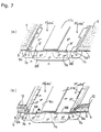
- Fig. 4 is an enlarged perspective view showing an IGBT semiconductor structure according to a second embodiment of the present invention.
- Fig. 5 is a graph showing the relationship between the surface position and the surface concentration in a cross section cut along the line A-A' of Fig. 4.
- the IGBT semiconductor structure of the present embodiment includes the outer-contact emitter region 7b adjacently formed outside the surface of the main emitter region 7a, small-depth n-type source region 9A formed in the surface of the outer-contact emitter region 7b, and small-depth n + -type source contact region 9B formed in the surface of the inner-contact emitter region 7c.
- the p + -type main emitter region 7a has comb-shaped expanded portions 7d which extend through the interface between the n-type source region 9A and the n + -type source contact region 9B up to the surface of these regions 9A, 9B.
- the n-type source region 9A is provided with narrowed portions interposed between the expanded portions 7d, and the diffusion resistance r S exists as parasitic elements in these narrowed portions. Since the portion of the n-source region 9A located right under the gate electrode 6 extends over the entire width of the electrode, a whole-width channel is provided right under the gate electrode 6 when a positive potential is applied to the electrode 6, assuring substantially the same channel resistance as that of the first embodiment.
- the potential of the n-type source region 9A also increases as compared with the that of the emitter electrode 8, due to the voltage drop of the diffusion resistance r S caused by electron current.
- the pn junction between the n-type source region 9A and the p-type outer-contact emitter region 7b is even less likely to forward-biased, as compared with the first embodiment, thus assuring increased ability to prevent latch-up. While no excess current flows in the normal on condition of the IGBT, however, the diffusion resistance r S is added as the ON-state voltage, resulting in an increase in the ON-state resistance compared to that of the first embodiment.
- the n + -type buffer layer 3 is laminated on the p + -type collector layer 2 to provide a semiconductor substrate 10, as shown in Fig. 2(a).
- the n - -type conductivity modulation layer (n base) 4 is then epitaxially grown on the n + -type buffer layer 3.
- an initial oxidation process is conducted so that the surface of the n - -type conductivity modulation layer 4 is covered with a thick silicon oxide film 11.
- a mask 11e having an opening 11a or forming the main emitter region 7a is formed from the silicon oxide film 11 by photolithography, as shown in Fig. 6(a).
- This opening 11a has opposite edges each having rectangular recesses 11d. Then, boron ions B + are implanted so as to dope acceptors, which are then driven into the n - -type conductivity modulation layer 4 so as to form the well-shaped p + -type main emitter region 7a. With the edges of the mask 11e having the rectangular recesses, the main emitter region 7a has rectangular protruding portions that are spaced along the edges of the well. Another oxidation process is then conducted, to cover the opening 11d with a thick silicon oxide film.
- a middle portion of the silicon oxide film on the main emitter region 7a is left as an implant mask 11c while the remaining portion is removed by photolithography.
- a gate oxidation process is conducted to form the gate insulating films 5, as shown in Fig. 6(b)
- the gate electrodes 6 made of polysilicon are formed on portions between adjacent main emitter regions 7a, 7a by photolithography.
- boron ions B + are implanted (channel doping) in a self-aligning manner using the silicon oxide film 11c and gate electrodes 6 as masks, to thus dope acceptors. Thereafter, channel driving is conducted so as to diffuse p-type regions into small-depth end portions of the well of the p + -type main emitter region 7a, so that the outer-contact emitter regions 7b are formed outside the well edges of the main emitter region 7a.
- the main emitter region 7a is provided with inner-contact emitter regions 7c that are heavily-doped regions of nearly p ++ type.
- a high concentration of phosphorus or arsenic ions are implanted as donors in a self-aligning manner using the silicon oxide film 11c and gate electrodes 6 as masks, to form small-depth n-type source layers 9' in surface layers of the main emitter region 7a and outer-contact emitter regions 7b.
- the n-type source regions 9A are formed in the surface layers of the outer-contact emitter regions 7b, while the p + -type regions 9B' are formed in the surface layers of the inner-contact emitter regions 7c of the main emitter region 7a.
- phospho-silicate glass (PSG) layers 12 serving as inter-layer insulation films are formed on the gate electrodes 6 by photolithography with contact holes 8a for forming the emitter electrode 8 being formed.
- the contact holes 8a are provided exactly on the p + -type regions 9B'.
- the end portions of the phospho-silicate glass layers 12 defining the contact holes 8a extend over the pn junctions formed between alternately arranged n and p + regions.
- a high concentration of phosphorus or arsenic ions are implanted again as donors through the contact holes 8a, using the phospho-silicate glass layers 12 and silicon oxide film 11c as masks, so as to increase the concentration of the inner regions of the n-type source layers 9 to thus form the n + -type source contact regions 9B.
- the portions of the source layers 9 located right under the phospho-silicate glass layers 12 remain as the n-type source regions 9A.
- the emitter electrode 8 made of aluminum is formed, as shown in Fig. 4.
- the collector electrode 1 is also formed on the rear surface of the p + -type collector layer 2, as shown in Fig. 1.
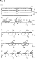
- Fig. 8(a) is a circuit diagram showing the circuit construction of IGBT according to a third embodiment of the present invention.
- Fig. 8(b) is a graph showing the relationship between the emitter-gate voltage and the collector saturation current.
- the IGBT 100 of the present embodiment is a composite IGBT combining a pnp-type first IGBT 1 having a low threshold voltage V TH1 and a pnp-type second IGBT 2 having a high threshold voltage V TH2 .
- the threshold voltage V TH2 of the second IGBT 2 is set to be higher than the threshold voltage V TH1 of the first IGBT 1, so that a difference between these threshold voltages V TH1 and V TH2 is on the order of 1V, which is much greater than a range of ⁇ 0.3V of errors between these threshold voltages encountered in a normal process.
- the lower threshold value V TH1 is set to 4V
- the higher threshold value V TH2 is set to 8V.
- the device size of the first IGBT 1 is made substantially equivalent to that of the second IGBT 2.
- the composite IGBT 100 of the present embodiment has a characteristic (solid line) of the collector saturation current Ic with respect to the emitter-gate voltage V GE , which is intermediate between the characteristic (one-dot chain line) of the first IGBT 1 with the lower threshold voltage V TH1 and that (broken line) of the second IGBT 2 with the higher threshold voltage V TH2 .
- a gate voltage V GE (of 15V, for example) which is considerably higher than the threshold voltage V TH1 is applied to the gate electrode. If a voltage equivalent to the supply voltage V CC is applied between the emitter and collector upon load short-circuiting, therefore, excess current flows through the first IGBT 1 with a result of breakdown.
- the ON-state voltage (collector saturation voltage) becomes high due to a small margin between the threshold voltage V TH2 and the gate voltage applied in normal switch-on operations.
- the integrated circuit of this type is not suitable for switching operations.
- the threshold voltage coincides with the threshold voltage V TH1 , and normal switch-on/off operations can be thus accomplished without any problem as in the first IGBT 1, and the ON-state voltage does not increase.
- the current value of the collector saturation current I C of the composite IGBT 100 is lower than that of the first IGBT upon load short-circuiting.
- the composite IGBT 100 shows improved capability to withstand load short-circuiting.
- Fig. 9 is a cross sectional view showing a first semiconductor structure which provides the composite IGBT 100 of Fig. 8(a).
- This semiconductor structure includes p-type, low-impurity-concentration emitter layers 17a in the form of wells formed in the surface of an n - -type conductivity modulation layer (n base) 4, and p-type, high-impurity-concentration emitter layers 17b in the form of wells formed in the surface of the conductivity modulation layer 4.
- each portion of the structure including an emitter layer 17a is part of the IGBT 1 having the low threshold voltage V TH1
- each portion including an emitter layer 17b is part of the IGBT 2 having the high threshold voltage V TH2 .
- the threshold voltage of the IGBT differs between two adjacent p-type wells.
- Fig. 10 is a cross sectional view showing a second semiconductor structure that provides the composite IGBT 100 of Fig. 8(a).
- this semiconductor structure one half (region A) of each p-type emitter layer (well) 17 is formed with a low impurity concentration, and the other half (region B) is formed with a high impurity concentration.
- each portion of the structure including a region A is part of the IGBT 1 having the low threshold voltage V TH1
- each portion of the structure including a region B is part of the IGBT 2 having the high threshold voltage V TH2 .
- Fig. 11 is a cross sectional view showing a third semiconductor structure which provides the composite IGBT 100 of Fig. 8(a).
- This semiconductor structure includes p-type emitter layers (wells) 17 in the form of planar stripes (only one being shown) formed in the surface of the n - -type conductivity modulation layer (n base) 4.
- Each emitter layer 17 has p-type low-concentration regions 17A and p-type high-concentration regions 17B that are alternately arranged in the longitudinal direction of the stripe-like layer 17.
- Each portion of the structure including a p-type low-concentration region 17A is part of the IGBT 1 having the low threshold voltage V TH1
- each portion including a p-type high-concentration region 17B is part of the IGBT 2 having the high threshold voltage V TH2 .
- Fig. 12(a) is a cross sectional view showing another semiconductor structure that realizes the composite IGBT 100.
- Fig. 12(b) is a graph showing the relationship between the collector saturation current and the emitter-gate voltage in the semiconductor structure of Fig. 12(a).
- This semiconductor structure includes p-type, low-impurity-concentration emitter layers 17a in the form of wells formed in the surface of the n - -type conductivity modulation layer (n base) 4, and p-type, high-impurity-concentration emitter layers 17b in the form of wells formed in the surface of the conductivity modulation layer 4.
- the channel length L a in the emitter layers 17a is made longer than the channel length L b in the emitter layers 17b.
- each portion of the structure including an emitter layer 17a is part of the IGBT 1 having the low threshold voltage V TH1
- each portion including an emitter layer 17b is part of the IGBT 2 having the high threshold voltage V TH2 .
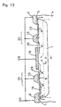
- Fig. 13 is a cross sectional view showing a semiconductor structure of IGBT according to a fourth embodiment of the present invention.
- the semiconductor structure of the present embodiment includes a p-type emitter layer (p base) 7 formed as a well in the surface of the conductivity modulation layer (n base) 4, and first gate electrodes 6 and second gate electrodes 16 made of polysilicon and formed on the conductivity modulation layer 4 through gate insulating films 5.
- the structure further includes n + -type source layers 19 and n + -type source contact layers 29 which are formed as wells in the surface of the emitter layer (p base) 7 in self-aligned manner using the first gate electrodes 6, 16 as masks, and an emitter electrode 18 made of aluminum and held in ohmic contact with both the n + -type source layers 29 and emitter layer 7.
- Each of the second gate electrodes 16 is formed so as to overlap the corresponding source layer 19 and source contact layer 29, to thus provide a switching lateral MOSFET 20 wherein the source layer 19 serves as a drain, and the source contact layer 29 serves as a source.
- the switching lateral MOSFET 20 When the IGBT is turned on with a positive potential applied to the first gate electrodes 6 and the second gate electrodes 16, the switching lateral MOSFET 20 is turned on so that electron current I E flows through an n channel of the switching lateral MOSFET 20. If load short-circuiting occurs, the switching lateral MOSFET 20 operates in a saturation region (non-linear region) in which the electron current I E is limited by the saturation current, and therefore excess current is unlikely to flow. Since this state is equivalent to occurrence of high channel resistance, the potential of the source layer 19 is increased to be higher than the potential of the emitter electrode 18, and the pn junction between the source layer 19 and the emitter layer 7 is less likely to be forward-biased, thus assuring high ability to prevent latch-up.
- the n-channel of the switching lateral MOSFET 20 disappears, and the conductance between the source layer 19 and the source contact layer 29 is interrupted, whereby the source layer 19 is held in a floating condition.
- the DMOS structure of the conventional IGBT as shown in Fig. 16 when the potential of the gate electrode 6 is dropped to be lower than the threshold voltage upon turn-off, the electron current is sharply reduced due to disappearance of a channel of DMOS, and latch-up may occur during a rapid increase in the emitter-collector voltage, with the pn junction between the source layer 9 and the emitter layer 7 being forward biased due to an increase in a hole current component.
- the source layer 19 is not grounded but brought into the floating condition upon turn-off, and thus latch-up does not occur even with the above pn junction being forward biased.
- Fig. 14(a) shows a planar pattern of the semiconductor structure of Fig. 13
- Fig. 14(b) is a cross sectional view taken along line A-A' of Fig. 14(a)
- Fig. 14(c) is a cross sectional view taken along line B-B' of Fig. 14(a).
- the n + -type source layer 19 consists of a channel-width equivalent portion 19a (i.e., a portion having a width corresponding to that of the channel width; note that the channel width is the vertical dimension as seen in Fig. 14(A) and the direction perpendicular to the paper plane as seen in Fig. 13) located right under the edge of the strip gate electrode 6, and a small-width portion 19b (i.e.
- the diffusion resistance r S exists as a parasitic element in the small-width portion 19b, as well as the channel resistance r C of the switching lateral MOSFET 20. This leads to improved capability to withstand load short-circuiting.
- Fig. 15(a) shows a planar pattern of an improvement of the structure shown in Fig. 14, Fig. 15(b) is a cross sectional view taken along line A-A' of Fig. 15(a), and Fig. 15(c) is a cross sectional view taken along line B-B' of Fig. 15(a).
- the diffusion resistance r B in the path of hole current I H is increased due to an increased distance between the source layer 19 as a source for injecting the electron current I E and the emitter electrode 18 for collecting the hole current I H . Therefore, the diffusion resistance r B needs to be further lowered.
- second emitter electrodes 28 are provided for collecting only the hole current I H , so that the first emitter electrode 18 serves as a source for injecting only the electron current I E .
- the second emitter electrodes 28 are disposed between adjacent small-width portions 19b of the source layer 19.
- Second gate electrodes 26 are formed in strip shape, and an n + -type source contact layer 39 is also formed in the shape of a strip to extend in parallel with the electrode 26. Since the second emitter electrodes 28 are formed adjacent to the source layer 19, the length of the path of the hole current I H in the emitter layer 7 is reduced, and the diffusion resistance r B is lowered, thereby assuring further improved capability to withstand load short-circuiting.
- npn-type IGBT may be easily provided by inverting the conductivity type.
- the present invention yields the following effects.
Landscapes
- Engineering & Computer Science (AREA)
- Microelectronics & Electronic Packaging (AREA)
- Power Engineering (AREA)
- Physics & Mathematics (AREA)
- Ceramic Engineering (AREA)
- Condensed Matter Physics & Semiconductors (AREA)
- General Physics & Mathematics (AREA)
- Computer Hardware Design (AREA)
- Bipolar Transistors (AREA)
- Insulated Gate Type Field-Effect Transistor (AREA)
Applications Claiming Priority (2)
| Application Number | Priority Date | Filing Date | Title |
|---|---|---|---|
| JP13680196A JP3209091B2 (ja) | 1996-05-30 | 1996-05-30 | 絶縁ゲートバイポーラトランジスタを備えた半導体装置 |
| JP136801/96 | 1996-05-30 |
Publications (2)
| Publication Number | Publication Date |
|---|---|
| EP0810671A2 true EP0810671A2 (de) | 1997-12-03 |
| EP0810671A3 EP0810671A3 (de) | 1999-01-07 |
Family
ID=15183843
Family Applications (1)
| Application Number | Title | Priority Date | Filing Date |
|---|---|---|---|
| EP97108307A Withdrawn EP0810671A3 (de) | 1996-05-30 | 1997-05-22 | Halbleiterbauelement vom Isolationsgate-Bipolartransistortyp |
Country Status (3)
| Country | Link |
|---|---|
| US (1) | US5894139A (de) |
| EP (1) | EP0810671A3 (de) |
| JP (1) | JP3209091B2 (de) |
Cited By (6)
| Publication number | Priority date | Publication date | Assignee | Title |
|---|---|---|---|---|
| DE19750413A1 (de) * | 1997-11-14 | 1999-05-20 | Asea Brown Boveri | Bipolartransistor mit isolierter Steuerelektrode (IGBT) |
| EP1067607A2 (de) * | 1999-07-05 | 2001-01-10 | Fuji Electric Co. Ltd. | Transistor mit isoliertem Gate und Verfahren zur Herstellung |
| EP1104027A2 (de) * | 1999-11-29 | 2001-05-30 | Intersil Corporation | Leistungshalbleiteranordnung mit einem Ballastwiderstandsbereich |
| FR2810160A1 (fr) * | 2000-06-07 | 2001-12-14 | Mitsubishi Electric Corp | Dispositif a semiconducteur |
| EP1450411A1 (de) * | 2003-02-21 | 2004-08-25 | STMicroelectronics S.r.l. | MOS-Leistungsbauelement mit hoher Integrationsdichte und dessen Herstellungsverfahren |
| CN102299150A (zh) * | 2010-06-22 | 2011-12-28 | 茂达电子股份有限公司 | 具有可调输出电容值的功率半导体组件以及制作方法 |
Families Citing this family (17)
| Publication number | Priority date | Publication date | Assignee | Title |
|---|---|---|---|---|
| JP3149773B2 (ja) * | 1996-03-18 | 2001-03-26 | 富士電機株式会社 | 電流制限回路を備えた絶縁ゲートバイポーラトランジスタ |
| JP4164962B2 (ja) * | 1999-10-08 | 2008-10-15 | 株式会社デンソー | 絶縁ゲート型バイポーラトランジスタ |
| AU2001283217A1 (en) * | 2000-08-08 | 2002-02-18 | Advanced Power Technology, Inc. | Power mos device with asymmetrical channel structure |
| JP3979258B2 (ja) * | 2002-05-21 | 2007-09-19 | 富士電機デバイステクノロジー株式会社 | Mis半導体装置およびその製造方法 |
| JP4830263B2 (ja) * | 2004-04-26 | 2011-12-07 | 富士電機株式会社 | 高耐圧絶縁ゲート形バイポーラトランジスタ |
| JP5036234B2 (ja) * | 2006-07-07 | 2012-09-26 | 三菱電機株式会社 | 半導体装置 |
| JP4857353B2 (ja) * | 2009-03-02 | 2012-01-18 | 株式会社日立製作所 | 半導体装置、およびそれを用いたプラズマディスプレイ駆動用半導体装置 |
| TWI424564B (zh) * | 2011-01-13 | 2014-01-21 | Anpec Electronics Corp | Insulator gate with high operational response speed |
| US9024413B2 (en) | 2013-01-17 | 2015-05-05 | Infineon Technologies Ag | Semiconductor device with IGBT cell and desaturation channel structure |
| JP6500579B2 (ja) * | 2015-04-28 | 2019-04-17 | セイコーエプソン株式会社 | 回路装置、電子機器及び移動体 |
| US9780202B2 (en) | 2015-08-31 | 2017-10-03 | Ixys Corporation | Trench IGBT with waved floating P-well electron injection |
| US10367085B2 (en) | 2015-08-31 | 2019-07-30 | Littelfuse, Inc. | IGBT with waved floating P-Well electron injection |
| US9780168B2 (en) * | 2015-08-31 | 2017-10-03 | Ixys Corporation | IGBT with waved floating P-well electron injection |
| DE102015117994B8 (de) | 2015-10-22 | 2018-08-23 | Infineon Technologies Ag | Leistungshalbleitertransistor mit einer vollständig verarmten Kanalregion |
| DE102016118012A1 (de) * | 2016-09-23 | 2018-03-29 | Infineon Technologies Ag | Halbleiterbauelement und Verfahren zum Bilden eines Halbleiterbauelements |
| JP6280629B2 (ja) * | 2016-12-15 | 2018-02-14 | 株式会社東芝 | 半導体装置 |
| JP6869376B2 (ja) * | 2017-12-21 | 2021-05-12 | 三菱電機株式会社 | 半導体装置 |
Citations (13)
| Publication number | Priority date | Publication date | Assignee | Title |
|---|---|---|---|---|
| DE3519389A1 (de) * | 1984-05-30 | 1985-12-19 | Kabushiki Kaisha Toshiba, Kawasaki, Kanagawa | Mosfet mit veraenderlicher leitfaehigkeit |
| JPS62266871A (ja) * | 1986-05-15 | 1987-11-19 | Fuji Electric Co Ltd | たて形mosfet |
| JPS6384164A (ja) * | 1986-09-29 | 1988-04-14 | Nissan Motor Co Ltd | 縦形mosfet |
| US4857983A (en) * | 1987-05-19 | 1989-08-15 | General Electric Company | Monolithically integrated semiconductor device having bidirectional conducting capability and method of fabrication |
| EP0336393A2 (de) * | 1988-04-05 | 1989-10-11 | Kabushiki Kaisha Toshiba | Halbleiteranordnung, deren Struktur die Wirkung des parasitischen Transistors erschwert und Verfahren zur Herstellung |
| JPH02106073A (ja) * | 1988-10-15 | 1990-04-18 | Fuji Electric Co Ltd | 伝導度変調型mosfetの製造方法 |
| JPH0411780A (ja) * | 1990-04-30 | 1992-01-16 | Nippondenso Co Ltd | 絶縁ゲート型バイポーラトランジスタ |
| JPH04196174A (ja) * | 1990-11-26 | 1992-07-15 | Fuji Electric Co Ltd | 絶縁ゲートバイポーラトランジスタ |
| EP0538004A2 (de) * | 1991-10-14 | 1993-04-21 | Mitsubishi Denki Kabushiki Kaisha | Feldeffekt-Halbleiteranordnung und Verfahren zur Herstellung |
| EP0561267A2 (de) * | 1992-03-18 | 1993-09-22 | Mitsubishi Denki Kabushiki Kaisha | Halbleiterbauelement mit isoliertem Gate und dessen Herstellungsverfahren |
| EP0581246A2 (de) * | 1992-07-28 | 1994-02-02 | Fuji Electric Co., Ltd. | Halbleiterbauelement vom MOS-Typ |
| US5378903A (en) * | 1993-03-23 | 1995-01-03 | Fuji Electric Co., Ltd. | Semiconductor device with low on-voltage and large controllable turn-off current |
| EP0658940A1 (de) * | 1993-11-23 | 1995-06-21 | Siemens Aktiengesellschaft | Durch Feldeffekt steuerbares Halbleiterbauelement |
Family Cites Families (5)
| Publication number | Priority date | Publication date | Assignee | Title |
|---|---|---|---|---|
| US5338693A (en) * | 1987-01-08 | 1994-08-16 | International Rectifier Corporation | Process for manufacture of radiation resistant power MOSFET and radiation resistant power MOSFET |
| JPH0783117B2 (ja) * | 1988-04-15 | 1995-09-06 | 三菱電機株式会社 | 半導体装置 |
| JP2752184B2 (ja) * | 1989-09-11 | 1998-05-18 | 株式会社東芝 | 電力用半導体装置 |
| US5247207A (en) * | 1989-12-20 | 1993-09-21 | National Semiconductor Corporation | Signal bus line driver circuit |
| US5296725A (en) * | 1992-06-10 | 1994-03-22 | North Carolina State University At Raleigh | Integrated multicelled semiconductor switching device for high current applications |
-
1996
- 1996-05-30 JP JP13680196A patent/JP3209091B2/ja not_active Expired - Fee Related
-
1997
- 1997-05-22 EP EP97108307A patent/EP0810671A3/de not_active Withdrawn
- 1997-05-28 US US08/864,290 patent/US5894139A/en not_active Expired - Fee Related
Patent Citations (13)
| Publication number | Priority date | Publication date | Assignee | Title |
|---|---|---|---|---|
| DE3519389A1 (de) * | 1984-05-30 | 1985-12-19 | Kabushiki Kaisha Toshiba, Kawasaki, Kanagawa | Mosfet mit veraenderlicher leitfaehigkeit |
| JPS62266871A (ja) * | 1986-05-15 | 1987-11-19 | Fuji Electric Co Ltd | たて形mosfet |
| JPS6384164A (ja) * | 1986-09-29 | 1988-04-14 | Nissan Motor Co Ltd | 縦形mosfet |
| US4857983A (en) * | 1987-05-19 | 1989-08-15 | General Electric Company | Monolithically integrated semiconductor device having bidirectional conducting capability and method of fabrication |
| EP0336393A2 (de) * | 1988-04-05 | 1989-10-11 | Kabushiki Kaisha Toshiba | Halbleiteranordnung, deren Struktur die Wirkung des parasitischen Transistors erschwert und Verfahren zur Herstellung |
| JPH02106073A (ja) * | 1988-10-15 | 1990-04-18 | Fuji Electric Co Ltd | 伝導度変調型mosfetの製造方法 |
| JPH0411780A (ja) * | 1990-04-30 | 1992-01-16 | Nippondenso Co Ltd | 絶縁ゲート型バイポーラトランジスタ |
| JPH04196174A (ja) * | 1990-11-26 | 1992-07-15 | Fuji Electric Co Ltd | 絶縁ゲートバイポーラトランジスタ |
| EP0538004A2 (de) * | 1991-10-14 | 1993-04-21 | Mitsubishi Denki Kabushiki Kaisha | Feldeffekt-Halbleiteranordnung und Verfahren zur Herstellung |
| EP0561267A2 (de) * | 1992-03-18 | 1993-09-22 | Mitsubishi Denki Kabushiki Kaisha | Halbleiterbauelement mit isoliertem Gate und dessen Herstellungsverfahren |
| EP0581246A2 (de) * | 1992-07-28 | 1994-02-02 | Fuji Electric Co., Ltd. | Halbleiterbauelement vom MOS-Typ |
| US5378903A (en) * | 1993-03-23 | 1995-01-03 | Fuji Electric Co., Ltd. | Semiconductor device with low on-voltage and large controllable turn-off current |
| EP0658940A1 (de) * | 1993-11-23 | 1995-06-21 | Siemens Aktiengesellschaft | Durch Feldeffekt steuerbares Halbleiterbauelement |
Non-Patent Citations (7)
| Title |
|---|
| HAGINO H ET AL: "AN EXPERIMENTAL AND NUMERICAL STUDY ON THE FORWARD BIASED SOA OF IGBT'S" 1 March 1996 , IEEE TRANSACTIONS ON ELECTRON DEVICES, VOL. 43, NR. 3, PAGE(S) 490 - 500 XP000588568 * page 491, column 2, paragraph 3 - page 492, column 1, paragraph 1; figure 2C * * |
| PATENT ABSTRACTS OF JAPAN vol. 012, no. 150 (E-606), 10 May 1988 -& JP 62 266871 A (FUJI ELECTRIC CO LTD), 19 November 1987 * |
| PATENT ABSTRACTS OF JAPAN vol. 012, no. 320 (E-651), 30 August 1988 -& JP 63 084164 A (NISSAN MOTOR CO LTD), 14 April 1988 * |
| PATENT ABSTRACTS OF JAPAN vol. 014, no. 320 (E-0950), 10 July 1990 -& JP 02 106073 A (FUJI ELECTRIC CO LTD), 18 April 1990 * |
| PATENT ABSTRACTS OF JAPAN vol. 016, no. 162 (E-1192), 20 April 1992 -& JP 04 011780 A (NIPPONDENSO CO LTD), 16 January 1992 * |
| PATENT ABSTRACTS OF JAPAN vol. 016, no. 521 (E-1285), 27 October 1992 & JP 04 196174 A (FUJI ELECTRIC CO LTD), 15 July 1992 * |
| ZENG J ET AL: "DESIGN OF IGBTS FOR LATCH-UP FREE OPERATION" 1 August 1994 , SOLID STATE ELECTRONICS, VOL. 37, NR. 8, PAGE(S) 1471 - 1475 XP000453718 * abstract; figure 1 * * |
Cited By (12)
| Publication number | Priority date | Publication date | Assignee | Title |
|---|---|---|---|---|
| DE19750413A1 (de) * | 1997-11-14 | 1999-05-20 | Asea Brown Boveri | Bipolartransistor mit isolierter Steuerelektrode (IGBT) |
| EP1067607A2 (de) * | 1999-07-05 | 2001-01-10 | Fuji Electric Co. Ltd. | Transistor mit isoliertem Gate und Verfahren zur Herstellung |
| EP1067607A3 (de) * | 1999-07-05 | 2003-08-06 | Fuji Electric Co. Ltd. | Transistor mit isoliertem Gate und Verfahren zur Herstellung |
| EP1104027A2 (de) * | 1999-11-29 | 2001-05-30 | Intersil Corporation | Leistungshalbleiteranordnung mit einem Ballastwiderstandsbereich |
| EP1104027A3 (de) * | 1999-11-29 | 2004-02-18 | Intersil Corporation | Leistungshalbleiteranordnung mit einem Ballastwiderstandsbereich |
| KR100749979B1 (ko) * | 1999-11-29 | 2007-08-16 | 페어차일드 세미컨덕터 코포레이션 | 전력 소자의 단락 회로 내구력을 개선하기 위한 강화된바디 효과가 있는 에미터 안정 저항기 |
| FR2810160A1 (fr) * | 2000-06-07 | 2001-12-14 | Mitsubishi Electric Corp | Dispositif a semiconducteur |
| DE10127391B4 (de) * | 2000-06-07 | 2013-12-24 | Mitsubishi Denki K.K. | Halbleiter-Vorrichtung |
| EP1450411A1 (de) * | 2003-02-21 | 2004-08-25 | STMicroelectronics S.r.l. | MOS-Leistungsbauelement mit hoher Integrationsdichte und dessen Herstellungsverfahren |
| US7091558B2 (en) | 2003-02-21 | 2006-08-15 | Stmicroelectronics S.R.L. | MOS power device with high integration density and manufacturing process thereof |
| CN102299150A (zh) * | 2010-06-22 | 2011-12-28 | 茂达电子股份有限公司 | 具有可调输出电容值的功率半导体组件以及制作方法 |
| CN102299150B (zh) * | 2010-06-22 | 2013-06-12 | 茂达电子股份有限公司 | 具有可调输出电容值的功率半导体组件以及制作方法 |
Also Published As
| Publication number | Publication date |
|---|---|
| JP3209091B2 (ja) | 2001-09-17 |
| US5894139A (en) | 1999-04-13 |
| EP0810671A3 (de) | 1999-01-07 |
| JPH09321290A (ja) | 1997-12-12 |
Similar Documents
| Publication | Publication Date | Title |
|---|---|---|
| US5894139A (en) | Semiconductor device structure for insulated gate bipolar transistor | |
| US5105243A (en) | Conductivity-modulation metal oxide field effect transistor with single gate structure | |
| US7968940B2 (en) | Insulated gate bipolar transistor device comprising a depletion-mode MOSFET | |
| JP3469967B2 (ja) | 電力装置集積化構造体 | |
| EP0110331B1 (de) | MOS-Transistor | |
| US20090057711A1 (en) | Semiconductor device with a u-shape drift region | |
| JPH08264764A (ja) | 半導体装置 | |
| US20030096481A1 (en) | Self-alignment of seperated regions in a lateral MOSFET structure of an integrated circuit | |
| US7180158B2 (en) | Semiconductor device and method of manufacture | |
| US4975751A (en) | High breakdown active device structure with low series resistance | |
| JP2590863B2 (ja) | 導電変調型mosfet | |
| EP0658939A2 (de) | Spannungsgesteuerter Thyristor und Verfahren zu seiner Herstellung | |
| JP2718907B2 (ja) | Pic構造体及びその製造方法 | |
| JPH0851197A (ja) | 電流飽和特性を有するmos制御サイリスタ | |
| JPH10501103A (ja) | Ligbt素子が形成されている半導体装置 | |
| US5237186A (en) | Conductivity-modulation metal oxide field effect transistor with single gate structure | |
| JP3522887B2 (ja) | 高耐圧半導体素子 | |
| JPH0855860A (ja) | 半導体装置 | |
| JP3063278B2 (ja) | 縦型電界効果トランジスタ | |
| JPH0992826A (ja) | 半導体素子及びそのシミュレーション方法 | |
| US6147382A (en) | Semiconductor switching device with segmented sources | |
| US11532710B2 (en) | Laterally diffused metal oxide semiconductor device with isolation structures for recovery charge removal | |
| JPH06275818A (ja) | 電力用半導体素子 | |
| JP3249175B2 (ja) | 絶縁ゲート付きサイリスタ及び高耐圧半導体装置 | |
| EP0845813A1 (de) | Bipolartransistor mit isolierter Gateelektrode |
Legal Events
| Date | Code | Title | Description |
|---|---|---|---|
| PUAI | Public reference made under article 153(3) epc to a published international application that has entered the european phase |
Free format text: ORIGINAL CODE: 0009012 |
|
| AK | Designated contracting states |
Kind code of ref document: A2 Designated state(s): CH DE LI |
|
| PUAL | Search report despatched |
Free format text: ORIGINAL CODE: 0009013 |
|
| AK | Designated contracting states |
Kind code of ref document: A3 Designated state(s): CH DE LI |
|
| 17P | Request for examination filed |
Effective date: 19990525 |
|
| STAA | Information on the status of an ep patent application or granted ep patent |
Free format text: STATUS: THE APPLICATION IS DEEMED TO BE WITHDRAWN |
|
| 18D | Application deemed to be withdrawn |
Effective date: 20060220 |