EP0649566B1 - Verfahren zur herstellung von speicherkondensatoren für dram-zellen - Google Patents
Verfahren zur herstellung von speicherkondensatoren für dram-zellen Download PDFInfo
- Publication number
- EP0649566B1 EP0649566B1 EP93912589A EP93912589A EP0649566B1 EP 0649566 B1 EP0649566 B1 EP 0649566B1 EP 93912589 A EP93912589 A EP 93912589A EP 93912589 A EP93912589 A EP 93912589A EP 0649566 B1 EP0649566 B1 EP 0649566B1
- Authority
- EP
- European Patent Office
- Prior art keywords
- layer
- auxiliary layer
- sio
- dummies
- storage
- Prior art date
- Legal status (The legal status is an assumption and is not a legal conclusion. Google has not performed a legal analysis and makes no representation as to the accuracy of the status listed.)
- Expired - Lifetime
Links
- 238000003860 storage Methods 0.000 title claims abstract description 67
- 238000000034 method Methods 0.000 title claims abstract description 32
- 239000003990 capacitor Substances 0.000 title claims abstract description 28
- 229910021420 polycrystalline silicon Inorganic materials 0.000 claims abstract description 43
- 229920005591 polysilicon Polymers 0.000 claims abstract description 43
- VYPSYNLAJGMNEJ-UHFFFAOYSA-N Silicium dioxide Chemical compound O=[Si]=O VYPSYNLAJGMNEJ-UHFFFAOYSA-N 0.000 claims abstract description 30
- 229910052681 coesite Inorganic materials 0.000 claims abstract description 15
- 229910052906 cristobalite Inorganic materials 0.000 claims abstract description 15
- 239000000377 silicon dioxide Substances 0.000 claims abstract description 15
- 229910052682 stishovite Inorganic materials 0.000 claims abstract description 15
- 229910052905 tridymite Inorganic materials 0.000 claims abstract description 15
- 239000000758 substrate Substances 0.000 claims description 27
- 238000005530 etching Methods 0.000 claims description 25
- 229920002120 photoresistant polymer Polymers 0.000 claims description 21
- 230000008021 deposition Effects 0.000 claims description 15
- 238000001312 dry etching Methods 0.000 claims description 7
- 229910052581 Si3N4 Inorganic materials 0.000 claims 7
- 238000000151 deposition Methods 0.000 abstract description 13
- 238000004519 manufacturing process Methods 0.000 abstract description 8
- 235000012239 silicon dioxide Nutrition 0.000 abstract 2
- 229910004298 SiO 2 Inorganic materials 0.000 description 31
- 239000004642 Polyimide Substances 0.000 description 4
- 229920001721 polyimide Polymers 0.000 description 4
- 230000015572 biosynthetic process Effects 0.000 description 3
- 238000003631 wet chemical etching Methods 0.000 description 3
- 238000005516 engineering process Methods 0.000 description 2
- 229910017855 NH 4 F Inorganic materials 0.000 description 1
- XUIMIQQOPSSXEZ-UHFFFAOYSA-N Silicon Chemical compound [Si] XUIMIQQOPSSXEZ-UHFFFAOYSA-N 0.000 description 1
- OEYIOHPDSNJKLS-UHFFFAOYSA-N choline Chemical compound C[N+](C)(C)CCO OEYIOHPDSNJKLS-UHFFFAOYSA-N 0.000 description 1
- 229960001231 choline Drugs 0.000 description 1
- 239000002131 composite material Substances 0.000 description 1
- 238000001020 plasma etching Methods 0.000 description 1
- 238000007781 pre-processing Methods 0.000 description 1
- 238000004886 process control Methods 0.000 description 1
- 229910052710 silicon Inorganic materials 0.000 description 1
- 239000010703 silicon Substances 0.000 description 1
Images

Classifications
-
- H—ELECTRICITY
- H10—SEMICONDUCTOR DEVICES; ELECTRIC SOLID-STATE DEVICES NOT OTHERWISE PROVIDED FOR
- H10B—ELECTRONIC MEMORY DEVICES
- H10B12/00—Dynamic random access memory [DRAM] devices
-
- H—ELECTRICITY
- H10—SEMICONDUCTOR DEVICES; ELECTRIC SOLID-STATE DEVICES NOT OTHERWISE PROVIDED FOR
- H10D—INORGANIC ELECTRIC SEMICONDUCTOR DEVICES
- H10D1/00—Resistors, capacitors or inductors
- H10D1/01—Manufacture or treatment
- H10D1/041—Manufacture or treatment of capacitors having no potential barriers
- H10D1/042—Manufacture or treatment of capacitors having no potential barriers using deposition processes to form electrode extensions
-
- H—ELECTRICITY
- H10—SEMICONDUCTOR DEVICES; ELECTRIC SOLID-STATE DEVICES NOT OTHERWISE PROVIDED FOR
- H10B—ELECTRONIC MEMORY DEVICES
- H10B12/00—Dynamic random access memory [DRAM] devices
- H10B12/01—Manufacture or treatment
- H10B12/02—Manufacture or treatment for one transistor one-capacitor [1T-1C] memory cells
- H10B12/03—Making the capacitor or connections thereto
- H10B12/033—Making the capacitor or connections thereto the capacitor extending over the transistor
-
- H—ELECTRICITY
- H10—SEMICONDUCTOR DEVICES; ELECTRIC SOLID-STATE DEVICES NOT OTHERWISE PROVIDED FOR
- H10D—INORGANIC ELECTRIC SEMICONDUCTOR DEVICES
- H10D1/00—Resistors, capacitors or inductors
- H10D1/60—Capacitors
- H10D1/68—Capacitors having no potential barriers
- H10D1/692—Electrodes
- H10D1/711—Electrodes having non-planar surfaces, e.g. formed by texturisation
- H10D1/716—Electrodes having non-planar surfaces, e.g. formed by texturisation having vertical extensions
-
- Y—GENERAL TAGGING OF NEW TECHNOLOGICAL DEVELOPMENTS; GENERAL TAGGING OF CROSS-SECTIONAL TECHNOLOGIES SPANNING OVER SEVERAL SECTIONS OF THE IPC; TECHNICAL SUBJECTS COVERED BY FORMER USPC CROSS-REFERENCE ART COLLECTIONS [XRACs] AND DIGESTS
- Y10—TECHNICAL SUBJECTS COVERED BY FORMER USPC
- Y10S—TECHNICAL SUBJECTS COVERED BY FORMER USPC CROSS-REFERENCE ART COLLECTIONS [XRACs] AND DIGESTS
- Y10S438/00—Semiconductor device manufacturing: process
- Y10S438/942—Masking
- Y10S438/947—Subphotolithographic processing
Definitions
- a stacked-capacitor DRAM cell comprises a MOS transistor and a storage capacitor, the MOS transistor being arranged in a silicon substrate and the storage capacitor consisting of two doped polysilicon layers and an interposed dielectric layer which are arranged on the surface of the substrate .
- the storage capacitor completely or partially covers that area which is occupied by the transistor.
- the storage node ie the electrode of the storage capacitor on which the information is stored in the form of charge
- the bottom surface which is arranged on the surface of the substrate, it comprises a jacket surface which projects upwards.
- the dielectric layer is arranged on the surface of the bottom surface and on the inside and outside on the surface of the outer surface.
- the cell plate, ie the second electrode of the storage capacitor is then arranged on the surface of the dielectric layer. In this way, the area of the capacitor can be increased drastically compared to the area occupied on the substrate.
- an auxiliary layer is first produced on the surface of the substrate. Openings are made in this.
- a thin layer of doped polysilicon is deposited on the auxiliary layer with the openings. The part of the polysilicon layer deposited on the side walls and the bottom of the openings forms the later storage node.
- the side walls of the openings should therefore be as vertical as possible.
- a storage dielectric is applied over the entire surface. This runs both on the inner and on the outer surfaces of the free-standing jacket part of the storage node.
- the cell plate is then applied over the entire surface as a counter electrode.
- the auxiliary layer is applied to the surface of the substrate in which the MOS transistors were previously manufactured. A cell contact must be made between the storage node and the respective active region of the associated transistor. This can follow directly or via additional, electrically conductive structures.
- the surface of the substrate is usually covered with an insulating layer. When producing the opening in the auxiliary layer, it must be ensured that there is no uncontrolled structuring of the insulating layer lying under the auxiliary layer. If holes are created in the insulating layer in addition to the cell contacts to other conductive areas during the production of the openings, short circuits occur via these the storage node subsequently formed. This should be avoided.
- p. 69 to form a polysilicon support under the auxiliary layer which is formed from SiO 2 in the region of the storage node. This is produced before deposition of the auxiliary layer by deposition of a polysilicon layer over the entire area and subsequent structuring using a photoresist mask.
- the size of the polysilicon base is dimensioned so that the SiO 2 etching to form the opening in the auxiliary layer meets it securely. With this etching, the polysilicon base acts as an etching stop.
- the polysilicon pad remains in the memory cell as part of the later storage node.
- auxiliary layer From Y. Kawamoto et al, Symp. On VLSI-Technology 1990, p. 13 it is known to form the auxiliary layer from polyimide.
- the production of the openings in the auxiliary layer is then not critical since polyimide can be etched with good selectivity to SiO 2 .
- a polysilicon layer is deposited on the surface of the auxiliary polyimide layer in order to produce the storage nodes. Because of the low temperature stability of the polyimide, the temperature during the polysilicon deposition must be limited.
- DE-A-4 113 233 discloses a method for producing storage capacitors for DRAM cells.
- the invention is based on the problem of specifying a further method for producing storage capacitors for DRAM cells, which is suitable for use in the production of a stacked capacitor DRAM cell and in which an uncontrolled free etching of electrically conductive structures in the substrate during Production of openings in an auxiliary layer arranged on the surface of the substrate is reliably avoided.
- a first auxiliary layer made of polysilicon is deposited over the entire surface of a substrate provided with SiO 2 .
- Transistors and possibly electrical connecting elements are previously produced in the substrate.
- the first auxiliary layer is structured in accordance with the arrangement of the storage capacitors, so that it has openings which each run between storage nodes of adjacent storage capacitors.
- a second auxiliary layer made of SiO 2 is deposited over the entire surface, the openings in the first auxiliary layer being filled with SiO 2 .
- SiO 2 can be etched with good selectivity to polysilicon, so that the surface of the first auxiliary layer is exposed in a selective etching process by etching back the second auxiliary layer.
- SiO 2 remains in the openings as a placeholder.
- the first auxiliary layer is selectively completely removed to SiO 2 , so that the placeholders remain.
- the process control prior to the deposition of the first auxiliary layer in particular ensures that a conductive structure for connecting the storage nodes is only covered by a thin SiO 2 layer. This is removed by briefly etching back SiO 2 over the entire area.
- the storage nodes By depositing a doped polysilicon layer over the entire surface and exposing the surface of the placeholders in the upper area of the placeholders, the storage nodes are formed. In this way, the storage nodes completely cover the area within the placeholders and the side walls of the placeholders essentially. Storage nodes produced in this way are essentially cylindrical, the area within the placeholders forming the base area and the portion of the polysilicon layer arranged on the side walls of the placeholders forming the outer surface of a cylinder. After removing the placeholders selectively for the storage nodes, storage dielectric and a conductive layer as a cell plate are produced over the entire surface.
- the first auxiliary layer is formed from polysilicon and SiO 2 is continuously present under the first auxiliary layer and because polysilicon can be etched with good selectivity for SiO 2 , uncontrolled exposure of electrical structures below the SiO 2 is required when the openings in the first auxiliary layer are formed - Surface not to be feared.
- the first auxiliary layer is structured using a photoresist mask. All other structuring can be self-adjusted, i.e. H. done without another photoresist mask. A photoresist mask would be necessary anyway to structure the storage nodes. The introduction of additional photoresist masks is avoided in the method according to the invention.
- a photoresist layer to expose the surface in the upper region of the placeholder, which is removed by back-exposure and development only in the upper part of the placeholders covered with the doped polysilicon layer.
- the placeholder is e.g. B. removed by SiO 2 etching, in which the etching removal is set over the etching time.
- an Si 3 N 4 layer is deposited which is thinner than it corresponds to half the width of the openings in the first auxiliary layer.
- the surface of the Si 3 N 4 layer is exposed in the region of the first auxiliary layer.
- the surface of the first auxiliary layer is then exposed in an Si 3 N 4 etching selective to polysilicon.
- the placeholders are surrounded by the portion of the Si 3 N 4 layer surrounding them in the openings.
- the placeholders are removed by SiO 2 etching which is selective with respect to Si 3 N 4 .
- An Si 3 N 4 etching is then carried out selectively with respect to polysilicon and SiO 2 , the residues of the Si 3 N 4 layer being removed completely.
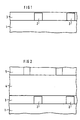
- the method according to the invention is based on a substrate 1 (see FIG. 1) in which transistors for a DRAM cell arrangement were previously produced. For the sake of clarity, these transistors are not shown in detail in FIG. 1.
- the substrate 1 comprises electrically conductive structures 2, via which the transistors are electrically connected to storage capacitors to be produced by the method according to the invention.
- An insulating layer 3 is provided on the surface of the substrate 1, which completely covers the electrically conductive structures 2 and other electrically conductive components, which are not shown.
- the insulating layer 3 consists essentially of SiO 2 .
- a first auxiliary layer 4 is applied to the entire surface of the insulating layer 3 (see FIG. 2).
- the first auxiliary layer 4 is made of polysilicon z. B. applied by CVD deposition.
- the first auxiliary layer 4 is z. B. 1 micron applied.
- the thickness of the first auxiliary layer 4 determines the height of the cylindrical side surfaces of the storage nodes to be produced later.
- a photoresist mask 5 is applied to the first auxiliary layer 4.
- the photoresist mask 5 is produced by depositing a photoresist layer, exposing and developing the photoresist layer. In a dry etching step, e.g. B.
- the first auxiliary layer 4 is structured using the photoresist mask 5 as an etching mask (see FIGS. 2 and 3). In the first auxiliary layer 4 Openings 6 formed. The openings 6 each run between locations at which storage nodes of adjacent storage capacitors are later produced. The remaining first auxiliary layer 4 covers those areas of the surface of the insulating layer 3 which are later covered by storage nodes.
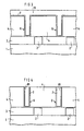
- An Si 3 N 4 layer 7 is subsequently covered over the entire surface in a thickness of, for. B. 20 nm deposited.
- a second auxiliary layer 8 is deposited over the entire surface of the Si 3 N 4 layer 7.
- the second auxiliary layer 8 is formed from SiO 2 .
- the second auxiliary layer 8 is deposited in such a thickness that the openings 6 are completely filled with SiO 2 .
- the thickness is z. B. 200 nm.
- the deposition of the second auxiliary layer 8 takes place, for. B. Compliant.
- the second auxiliary layer 8 is removed outside the openings 6.
- the surface of the Si 3 N 4 layer 7 is first exposed.
- the Si 3 N 4 layer 7 is removed from horizontal surfaces of the first auxiliary layer 4 made of polysilicon.
- the etching takes place selectively to polysilicon.
- the openings 6 remain filled with a placeholder 81 made of SiO 2 , which is the remainder of the second auxiliary layer 8.
- Si 3 N 4 of the Si 3 N 4 layer 7 remains arranged between the placeholder 81 and the surrounding first auxiliary layer 4 or the underlying insulating layer 3 (see FIG. 4).
- the first auxiliary layer 4 by wet chemical etching with z. B. Choline removed. This etching step is carried out selectively for SiO 2 and Si 3 N 4 . Since under the first auxiliary layer 4 the insulating layer 3 covers the entire surface is arranged from SiO 2 , it is ensured when removing the first auxiliary layer 4 that no uncontrolled etching into the insulating layer 3 takes place.
- the SiO 2 acts as an etch stop in the wet chemical etching.
- the insulating layer 3 above the electrically conductive structures 2 is subsequently removed in a dry etching process in order to open contact with the electrically conductive structures 2.
- the preprocessing must ensure that this dry etching process in SiO 2 can not produce undesired short circuits. This is done in particular by adjusting the layer thickness of the insulating layer 3.
- a doped polysilicon layer 9 is deposited over the entire surface in a thickness of z. B. 100 nm.
- the doped polysilicon layer 9 is deposited substantially conformally and completely covers the placeholder 81 (see FIG. 5).
- a photoresist layer is then deposited over the entire surface, which completely covers the doped polysilicon layer 9.
- the photoresist layer is back exposed and developed. During back exposure, the photoresist layer is exposed only to a predeterminable depth, so that only the upper part of the photoresist layer is removed during development.
- the photoresist layer is exposed to such an extent that a developed photoresist layer 10 is formed which leaves the upper part of the placeholders 81 covered with the doped polysilicon layer 9 uncovered (see FIG. 6).
- the doped polysilicon layer 9 is then structured in an anisotropic dry etching process in such a way that the horizontal surface of the placeholder 81 and the surrounding Si 3 N 4 of the Si 3 N 4 layer 7 is exposed. This creates storage nodes 91.
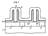
- the placeholders 81 are selectively removed from Si 3 N 4 and polysilicon in an etching step using NH 4 F, HF (5: 1).
- the Si 3 N 4 acts as an etch stop.
- the remaining part of the Si 3 N 4 layer 7 is then completely removed in a wet chemical etching process with hot HNO 3 .
- the Si 3 N 4 acts as an etch stop.
- the Si 3 N 4 layer 7 can be dispensed with. This leads to process simplification.
- a storage dielectric z. B produced by producing thermal SiO 2 , Si 3 N 4 and thermal SiO 2 .
- a cell plate 12 made of doped polysilicon is produced over the entire surface of the storage dielectric 11.
- the extent of the individual storage capacitors is determined by the geometry of the storage nodes 91 (see FIG. 7).
- the storage capacitor includes the surface of the inside and outside of the cylindrical part of the storage node 91.
- the storage nodes are connected to the corresponding transistors via the electrically conductive structures 2.
- the invention was explained on the basis of an exemplary embodiment in which the insulating layer 3 has a flat surface.
- the method according to the invention can be used analogously if the insulating layer is provided with a surface topology.
Landscapes
- Engineering & Computer Science (AREA)
- Manufacturing & Machinery (AREA)
- Semiconductor Memories (AREA)
- Semiconductor Integrated Circuits (AREA)
Applications Claiming Priority (3)
| Application Number | Priority Date | Filing Date | Title |
|---|---|---|---|
| DE4222467A DE4222467C1 (enExample) | 1992-07-08 | 1992-07-08 | |
| DE4222467 | 1992-07-08 | ||
| PCT/DE1993/000516 WO1994001891A1 (de) | 1992-07-08 | 1993-06-15 | Verfahren zur herstellung von speicherkondensatoren für dram-zellen |
Publications (2)
| Publication Number | Publication Date |
|---|---|
| EP0649566A1 EP0649566A1 (de) | 1995-04-26 |
| EP0649566B1 true EP0649566B1 (de) | 1997-11-26 |
Family
ID=6462779
Family Applications (1)
| Application Number | Title | Priority Date | Filing Date |
|---|---|---|---|
| EP93912589A Expired - Lifetime EP0649566B1 (de) | 1992-07-08 | 1993-06-15 | Verfahren zur herstellung von speicherkondensatoren für dram-zellen |
Country Status (8)
| Country | Link |
|---|---|
| US (1) | US5496757A (enExample) |
| EP (1) | EP0649566B1 (enExample) |
| JP (1) | JP3330605B2 (enExample) |
| KR (1) | KR100309614B1 (enExample) |
| AT (1) | ATE160652T1 (enExample) |
| DE (2) | DE4222467C1 (enExample) |
| TW (1) | TW358242B (enExample) |
| WO (1) | WO1994001891A1 (enExample) |
Families Citing this family (10)
| Publication number | Priority date | Publication date | Assignee | Title |
|---|---|---|---|---|
| DE19640273C1 (de) * | 1996-09-30 | 1998-03-12 | Siemens Ag | Verfahren zur Herstellung barrierenfreier Halbleiterspeicheranordnungen |
| US5998256A (en) * | 1996-11-01 | 1999-12-07 | Micron Technology, Inc. | Semiconductor processing methods of forming devices on a substrate, forming device arrays on a substrate, forming conductive lines on a substrate, and forming capacitor arrays on a substrate, and integrated circuitry |
| US6395613B1 (en) * | 2000-08-30 | 2002-05-28 | Micron Technology, Inc. | Semiconductor processing methods of forming a plurality of capacitors on a substrate, bit line contacts and method of forming bit line contacts |
| KR100227070B1 (ko) * | 1996-11-04 | 1999-10-15 | 구본준 | 커패시터 및 그의 제조방법 |
| US6590250B2 (en) | 1997-11-25 | 2003-07-08 | Micron Technology, Inc. | DRAM capacitor array and integrated device array of substantially identically shaped devices |
| JP2000077619A (ja) * | 1998-08-27 | 2000-03-14 | Oki Electric Ind Co Ltd | 半導体装置及びその製造方法 |
| US6157067A (en) | 1999-01-04 | 2000-12-05 | International Business Machines Corporation | Metal oxide semiconductor capacitor utilizing dummy lithographic patterns |
| KR100338959B1 (ko) * | 2000-08-31 | 2002-06-01 | 박종섭 | 반도체 소자의 커패시터 하부전극 제조방법 |
| KR100502410B1 (ko) | 2002-07-08 | 2005-07-19 | 삼성전자주식회사 | 디램 셀들 |
| US7468323B2 (en) * | 2004-02-27 | 2008-12-23 | Micron Technology, Inc. | Method of forming high aspect ratio structures |
Family Cites Families (5)
| Publication number | Priority date | Publication date | Assignee | Title |
|---|---|---|---|---|
| JPS62286270A (ja) * | 1986-06-05 | 1987-12-12 | Sony Corp | 半導体メモリ装置 |
| IT1245495B (it) * | 1990-01-26 | 1994-09-27 | Mitsubishi Electric Corp | Memoria ad accesso casuale dinamica avente un condensatore del tipo impilato e procedimento di fabbricazione di essa |
| DD299990A5 (de) * | 1990-02-23 | 1992-05-14 | Dresden Forschzentr Mikroelek | Ein-Transistor-Speicherzellenanordnung und Verfahren zu deren Herstellung |
| JP2519569B2 (ja) * | 1990-04-27 | 1996-07-31 | 三菱電機株式会社 | 半導体記憶装置およびその製造方法 |
| JPH0629483A (ja) * | 1991-04-29 | 1994-02-04 | Micron Technol Inc | スタック型iセルキャパシタおよびその製造方法 |
-
1992
- 1992-07-08 DE DE4222467A patent/DE4222467C1/de not_active Expired - Fee Related
-
1993
- 1993-06-15 JP JP50280694A patent/JP3330605B2/ja not_active Expired - Fee Related
- 1993-06-15 WO PCT/DE1993/000516 patent/WO1994001891A1/de not_active Ceased
- 1993-06-15 DE DE59307748T patent/DE59307748D1/de not_active Expired - Fee Related
- 1993-06-15 US US08/351,464 patent/US5496757A/en not_active Expired - Lifetime
- 1993-06-15 KR KR1019950700021A patent/KR100309614B1/ko not_active Expired - Fee Related
- 1993-06-15 EP EP93912589A patent/EP0649566B1/de not_active Expired - Lifetime
- 1993-06-15 AT AT93912589T patent/ATE160652T1/de not_active IP Right Cessation
- 1993-07-07 TW TW082105415A patent/TW358242B/zh not_active IP Right Cessation
Non-Patent Citations (2)
| Title |
|---|
| 1989 SYMPOSIUM ON VLSI TECHNOLOGY, Nr. 89/IEEE CAT., 22-25 Mai 1989, pp. 69,70; K. WAKAMIYA et al.: 'Novel stacked capacitor cell for 64Mb DRAM' * |
| IEEE Transactions on Electron Devices, Vol. 38, Nr. 2, Februar 1991, New York, US, pp. 255-261; KAGA et al.: 'Crown-shaped stacked-capacitor cell for 1.5-V operation 64-Mb DRAM's' * |
Also Published As
| Publication number | Publication date |
|---|---|
| KR100309614B1 (ko) | 2002-08-27 |
| EP0649566A1 (de) | 1995-04-26 |
| DE4222467C1 (enExample) | 1993-06-24 |
| US5496757A (en) | 1996-03-05 |
| HK1002337A1 (en) | 1998-08-14 |
| JP3330605B2 (ja) | 2002-09-30 |
| KR950702748A (ko) | 1995-07-29 |
| WO1994001891A1 (de) | 1994-01-20 |
| JPH07509346A (ja) | 1995-10-12 |
| ATE160652T1 (de) | 1997-12-15 |
| TW358242B (en) | 1999-05-11 |
| DE59307748D1 (de) | 1998-01-08 |
Similar Documents
| Publication | Publication Date | Title |
|---|---|---|
| DE4031411C2 (de) | Verfahren zur Herstellung einer einen Kondensator aufweisenden Halbleitervorrichtung | |
| DE19727232C2 (de) | Analoges integriertes Halbleiterbauelement und Verfahren zu dessen Herstellung | |
| DE4201506C2 (de) | Verfahren zur Herstellung von DRAM-Speicherzellen mit Stapelkondensatoren mit Flossenstruktur | |
| DE19933480A1 (de) | Zylindrischer Kondensator und Verfahren für dessen Herstellung | |
| DE4412089A1 (de) | Verfahren zur Herstellung eines Kondensators für ein hochintegriertes Halbleiterspeicherbauelement | |
| DE10007018A1 (de) | Halbleiterbauelemente mit Kondensator und Herstellungsverfahren hierfür | |
| WO2001001489A1 (de) | Dram-zellenanordnung und verfahren zu deren herstellung | |
| DE10347462A1 (de) | Bodenelektrode eines Kondensators einer Halbleitervorrichtung und Verfahren zur Herstellung derselben | |
| EP0649566B1 (de) | Verfahren zur herstellung von speicherkondensatoren für dram-zellen | |
| DE4327813C2 (de) | Verfahren zur Herstellung eines DRAM's | |
| DE4408565A1 (de) | Halbleiterspeichereinrichtung und Verfahren zu ihrer Herstellung | |
| DE19729602C2 (de) | Halbleitereinrichtung mit Kurzschlußverhinderung in der Verdrahtungsschicht und zugehöriges Herstellungsverfahren | |
| DE19925657A1 (de) | Verfahren zum Ausbilden eines selbstpositionierenden Kontakts in einem Halbleiterbauelement | |
| DE19860884A1 (de) | Verfahren zur Herstellung eines Dram-Zellenkondensators | |
| DE4328510A1 (de) | Verfahren zur Herstellung eines Halbleiterspeicherbauelementes mit einem Kondensator und damit herstellbares Halbleiterspeicherbauelement | |
| DE10012198B4 (de) | Zylindrisches Kondensatorbauelement mit innenseitigem HSG-Silicium und Verfahren zu seiner Herstellung | |
| DE4426311A1 (de) | Leiterbahnstruktur eines Halbleiterbauelementes und Verfahren zu ihrer Herstellung | |
| DE4034995A1 (de) | Hochintegriertes halbleiterspeicherbauelement und verfahren zu seiner herstellung | |
| DE10310080B4 (de) | Verfahren zum Ausbilden tieferer Gräben unabhängig von lithografisch bedingten, kritischen Abmessungen | |
| DE10351030A1 (de) | Transistorstruktur, Speicherzelle, DRAM und Verfahren zur Herstellung einer Transistorstruktur in einem Halbleitersubstrat | |
| DE4333989B4 (de) | Verfahren zur Herstellung eines Kondensators in einem Halbleiterspeicherbauelement | |
| DE60215513T2 (de) | Zweischichthartmaske zum ätzverfahren eines edram-gates | |
| DE4441166C2 (de) | Verfahren zur Herstellung eines Kondensators einer Halbleiterspeichervorrichtung | |
| DE19842684C1 (de) | Auf einem Stützgerüst angeordneter Kondensator in einer Halbleiteranordnung und Herstellverfahren | |
| DE19525576A1 (de) | Dünnfilmtransistor und Verfahren zu dessen Herstellung |
Legal Events
| Date | Code | Title | Description |
|---|---|---|---|
| PUAI | Public reference made under article 153(3) epc to a published international application that has entered the european phase |
Free format text: ORIGINAL CODE: 0009012 |
|
| 17P | Request for examination filed |
Effective date: 19941205 |
|
| AK | Designated contracting states |
Kind code of ref document: A1 Designated state(s): AT DE FR GB IE IT NL |
|
| GRAG | Despatch of communication of intention to grant |
Free format text: ORIGINAL CODE: EPIDOS AGRA |
|
| 17Q | First examination report despatched |
Effective date: 19970321 |
|
| GRAH | Despatch of communication of intention to grant a patent |
Free format text: ORIGINAL CODE: EPIDOS IGRA |
|
| GRAH | Despatch of communication of intention to grant a patent |
Free format text: ORIGINAL CODE: EPIDOS IGRA |
|
| GRAA | (expected) grant |
Free format text: ORIGINAL CODE: 0009210 |
|
| AK | Designated contracting states |
Kind code of ref document: B1 Designated state(s): AT DE FR GB IE IT NL |
|
| REF | Corresponds to: |
Ref document number: 160652 Country of ref document: AT Date of ref document: 19971215 Kind code of ref document: T |
|
| REF | Corresponds to: |
Ref document number: 59307748 Country of ref document: DE Date of ref document: 19980108 |
|
| ET | Fr: translation filed | ||
| ITF | It: translation for a ep patent filed | ||
| GBT | Gb: translation of ep patent filed (gb section 77(6)(a)/1977) |
Effective date: 19980127 |
|
| PGFP | Annual fee paid to national office [announced via postgrant information from national office to epo] |
Ref country code: AT Payment date: 19980604 Year of fee payment: 6 |
|
| PGFP | Annual fee paid to national office [announced via postgrant information from national office to epo] |
Ref country code: NL Payment date: 19980629 Year of fee payment: 6 |
|
| PLBE | No opposition filed within time limit |
Free format text: ORIGINAL CODE: 0009261 |
|
| STAA | Information on the status of an ep patent application or granted ep patent |
Free format text: STATUS: NO OPPOSITION FILED WITHIN TIME LIMIT |
|
| 26N | No opposition filed | ||
| PG25 | Lapsed in a contracting state [announced via postgrant information from national office to epo] |
Ref country code: AT Free format text: LAPSE BECAUSE OF NON-PAYMENT OF DUE FEES Effective date: 19990615 |
|
| PG25 | Lapsed in a contracting state [announced via postgrant information from national office to epo] |
Ref country code: NL Free format text: LAPSE BECAUSE OF NON-PAYMENT OF DUE FEES Effective date: 20000101 |
|
| NLV4 | Nl: lapsed or anulled due to non-payment of the annual fee |
Effective date: 20000101 |
|
| REG | Reference to a national code |
Ref country code: GB Ref legal event code: IF02 |
|
| PGFP | Annual fee paid to national office [announced via postgrant information from national office to epo] |
Ref country code: GB Payment date: 20060615 Year of fee payment: 14 |
|
| GBPC | Gb: european patent ceased through non-payment of renewal fee |
Effective date: 20070615 |
|
| PG25 | Lapsed in a contracting state [announced via postgrant information from national office to epo] |
Ref country code: GB Free format text: LAPSE BECAUSE OF NON-PAYMENT OF DUE FEES Effective date: 20070615 |
|
| PGFP | Annual fee paid to national office [announced via postgrant information from national office to epo] |
Ref country code: IT Payment date: 20080623 Year of fee payment: 16 |
|
| PGFP | Annual fee paid to national office [announced via postgrant information from national office to epo] |
Ref country code: IE Payment date: 20080619 Year of fee payment: 16 Ref country code: DE Payment date: 20080812 Year of fee payment: 16 |
|
| PGFP | Annual fee paid to national office [announced via postgrant information from national office to epo] |
Ref country code: FR Payment date: 20080613 Year of fee payment: 16 |
|
| REG | Reference to a national code |
Ref country code: FR Ref legal event code: ST Effective date: 20100226 |
|
| REG | Reference to a national code |
Ref country code: IE Ref legal event code: MM4A |
|
| PG25 | Lapsed in a contracting state [announced via postgrant information from national office to epo] |
Ref country code: IE Free format text: LAPSE BECAUSE OF NON-PAYMENT OF DUE FEES Effective date: 20090615 Ref country code: FR Free format text: LAPSE BECAUSE OF NON-PAYMENT OF DUE FEES Effective date: 20090630 |
|
| PG25 | Lapsed in a contracting state [announced via postgrant information from national office to epo] |
Ref country code: DE Free format text: LAPSE BECAUSE OF NON-PAYMENT OF DUE FEES Effective date: 20100101 |
|
| PG25 | Lapsed in a contracting state [announced via postgrant information from national office to epo] |
Ref country code: IT Free format text: LAPSE BECAUSE OF NON-PAYMENT OF DUE FEES Effective date: 20090615 |