EP0645805B1 - Method for mounting a semiconductor device on a circuit board, and a circuit board with a semiconductor device mounted thereon - Google Patents
Method for mounting a semiconductor device on a circuit board, and a circuit board with a semiconductor device mounted thereon Download PDFInfo
- Publication number
- EP0645805B1 EP0645805B1 EP94115187A EP94115187A EP0645805B1 EP 0645805 B1 EP0645805 B1 EP 0645805B1 EP 94115187 A EP94115187 A EP 94115187A EP 94115187 A EP94115187 A EP 94115187A EP 0645805 B1 EP0645805 B1 EP 0645805B1
- Authority
- EP
- European Patent Office
- Prior art keywords
- semiconductor device
- circuit board
- thermoplastic
- temperature
- conductive adhesive
- Prior art date
- Legal status (The legal status is an assumption and is not a legal conclusion. Google has not performed a legal analysis and makes no representation as to the accuracy of the status listed.)
- Expired - Lifetime
Links
Images


Classifications
-
- H10W72/20—
-
- H10W72/30—
-
- H10W74/012—
-
- H10W74/15—
-
- H10W72/072—
-
- H10W72/073—
-
- H10W72/251—
-
- H10W72/856—
-
- H10W90/724—
-
- H10W90/734—
-
- Y—GENERAL TAGGING OF NEW TECHNOLOGICAL DEVELOPMENTS; GENERAL TAGGING OF CROSS-SECTIONAL TECHNOLOGIES SPANNING OVER SEVERAL SECTIONS OF THE IPC; TECHNICAL SUBJECTS COVERED BY FORMER USPC CROSS-REFERENCE ART COLLECTIONS [XRACs] AND DIGESTS
- Y10—TECHNICAL SUBJECTS COVERED BY FORMER USPC
- Y10T—TECHNICAL SUBJECTS COVERED BY FORMER US CLASSIFICATION
- Y10T29/00—Metal working
- Y10T29/49—Method of mechanical manufacture
- Y10T29/49002—Electrical device making
- Y10T29/49117—Conductor or circuit manufacturing
- Y10T29/49124—On flat or curved insulated base, e.g., printed circuit, etc.
- Y10T29/49126—Assembling bases
-
- Y—GENERAL TAGGING OF NEW TECHNOLOGICAL DEVELOPMENTS; GENERAL TAGGING OF CROSS-SECTIONAL TECHNOLOGIES SPANNING OVER SEVERAL SECTIONS OF THE IPC; TECHNICAL SUBJECTS COVERED BY FORMER USPC CROSS-REFERENCE ART COLLECTIONS [XRACs] AND DIGESTS
- Y10—TECHNICAL SUBJECTS COVERED BY FORMER USPC
- Y10T—TECHNICAL SUBJECTS COVERED BY FORMER US CLASSIFICATION
- Y10T29/00—Metal working
- Y10T29/49—Method of mechanical manufacture
- Y10T29/49002—Electrical device making
- Y10T29/49117—Conductor or circuit manufacturing
- Y10T29/49124—On flat or curved insulated base, e.g., printed circuit, etc.
- Y10T29/4913—Assembling to base an electrical component, e.g., capacitor, etc.
-
- Y—GENERAL TAGGING OF NEW TECHNOLOGICAL DEVELOPMENTS; GENERAL TAGGING OF CROSS-SECTIONAL TECHNOLOGIES SPANNING OVER SEVERAL SECTIONS OF THE IPC; TECHNICAL SUBJECTS COVERED BY FORMER USPC CROSS-REFERENCE ART COLLECTIONS [XRACs] AND DIGESTS
- Y10—TECHNICAL SUBJECTS COVERED BY FORMER USPC
- Y10T—TECHNICAL SUBJECTS COVERED BY FORMER US CLASSIFICATION
- Y10T29/00—Metal working
- Y10T29/49—Method of mechanical manufacture
- Y10T29/49002—Electrical device making
- Y10T29/49117—Conductor or circuit manufacturing
- Y10T29/49124—On flat or curved insulated base, e.g., printed circuit, etc.
- Y10T29/49155—Manufacturing circuit on or in base
Definitions
- the present invention relates to a method for mounting a semiconductor device on a circuit board, and also relates to the circuit board with the semiconductor device mounted thereon. More particularly, the invention relates to a method for mounting a semiconductor device facedown on a circuit board by the use of a conductive adhesive, and also relates to the circuit board on which the semiconductor device is mounted by using this method.
- a circuit board can include a chip carrier or the like.
- thermoplastic conductive adhesive It is known from WO-A-8803704 a method to attach a semiconductor die to a circuit board by means of a thermoplastic conductive adhesive.
- a conventional encapsulating step follows to obtain a substrate with a semiconductor die mounted thereon comprising a joining layer formed of a thermoplastic conductive adhesive, the die being encapsulated by epoxy.
- JP-A-5218137 a method to bond a semiconductor element to a circuit board by means of a thermoplastic resin, and to fix the element to the board by curing a thermosetting resin covering the thermoplastic resin at a temperature lower than the plasticizing temperature of the thermoplastic resin.
- EP-A-332402 a method of manufacturing a connection construction for connecting a first conductor provided on a first member to a second conductor provided on a second member and disposed opposite to the first conductor.
- This method comprises the steps of depositing a conductive adhesive on the first conductor of the first member, hardening the conductive adhesive after bonding a conductive particle to the conductive adhesive with a portion thereof exposed, interposing the electrically insulating adhesive between the the first member and the second member and pressing the first member and the second member to each other and hardening the electrically insulating adhesive with the conductive particle contacting the second conductor.
- the conventional mounting method is disadvantageous in that a reliable connection between a semiconductor device and a circuit board cannot be obtained.
- the method for mounting a semiconductor device on a circuit board of the present invention includes the steps of :
- the above-mentioned method further includes the step of forming a bump electrode on the terminal electrode of the semiconductor device, the step being performed prior to the joining step.
- a circuit board with a semiconductor device mounted thereon includes:
- the above-mentioned circuit board further includes a bump electrode on the terminal electrode of the semiconductor device.
- thermoplastic conductive adhesive contains a thermoplastic resin and a conductive filler.
- thermosetting resin has a glass transition point equal to or higher than the maximum operating temperature for the semiconductor device.
- the plasticizing temperature of the thermoplastic conductive adhesive is equal to or higher than the maximum operating temperature for the semiconductor device.
- thermosetting resin is capable to maintain the compression force to the joining layer over the operating temperature range for the semiconductor device.
- the invention described herein makes possible the advantages of (1) providing a highly reliable circuit board with a semiconductor device mounted thereon, and (2) providing a method for mounting a semiconductor device on a circuit board with high reliability.
- a conductive adhesive layer 3 is formed using a thermoplastic conductive adhesive. Then, with the conductive adhesive layers 3 of the semiconductor device 1 aligned with corresponding connecting electrodes 5 of a circuit board 4 , the semiconductor device 1 is placed facedown (with its terminal electrodes 2 facing downward) on the circuit board 4 .
- thermoplastic conductive adhesive constituting the conductive adhesive layers 3 is heated at a temperature equal to or higher than its plasticizing temperature (e.g. 125°C), thereby improving the adhesion of the conductive adhesive layers 3 to the terminal electrodes 2 and to the connecting electrodes 5 .
- the thermoplastic conductive adhesive is then cooled to a temperature lower than the plasticizing temperature, e.g., it is cooled to room temperature (25°C), resulting in joining layers 6 as shown in Figure 1B .
- the terminal electrodes 2 of the semiconductor device 1 are electrically connected to and mechanically fixed to the corresponding connecting electrodes 5 of the circuit board 4 by means of the joining layers 6 formed of the thermoplastic conductive adhesive.
- thermosetting resin 7 e.g. an epoxy resin
- the liquid thermosetting resin 7 is then cured at a temperature equal or higher than the plasticizing temperature of the thermoplastic conductive adhesive used for the conductive adhesive layers 3 (e.g., it is cured at 150°C).
- thermosetting resin 7 While the thermosetting resin 7 is being cured, the thermoplastic conductive adhesive constituting the joining layers 6 is plasticized again.
- Figure 1C diagrammatically illustrates the curing of the thermosetting resin 7 , where the reference numeral 8 denotes the joining layers composed of the thus plasticized thermoplastic conductive adhesive.
- the liquid thermosetting resin 7 is cured and shrinks, thereby forming a cured resin layer 9 .
- the compression force of the cured resin layer 9 is applied to the plasticized joining layers 8 , so that the adhesion of the joining layers 8 to the semiconductor device 1 and to the circuit board 4 is improved, thereby improving the stability of the connection between the semiconductor device 1 and the circuit board 4 .
- the liquid thermosetting resin 7 used herein is a thermosetting resin which is cured at temperatures equal to or higher than the plasticizing temperature of the thermoplastic conductive adhesive used for the conductive adhesive layer 3 .
- thermosetting resin After the thermosetting resin has been cured, it is cooled to a temperature lower than the plasticizing temperature of the thermoplastic conductive adhesive, thereby allowing the plasticized joining layers 8 to solidify and turn into the joining layers 6 again.
- the circuit board 4 with the semiconductor device 1 mounted thereon is obtained as shown in Figure 1D , in which the semiconductor device 1 is electrically connected to the circuit board 4 by the joining layers 6 of the thermoplastic conductive adhesive, and the gap between the semiconductor device 1 and the circuit board 4 is filled with the cured resin layer 9 .
- the semiconductor device 1 is joined to the circuit board 4 by means of the joining layers 6 made of the thermoplastic conductive adhesive, and the gap between the semiconductor device 1 and the circuit board 4 is filled with the resin layer 9 made of the thermosetting resin. Accordingly, the joining layers 6 of the thermoplastic conductive adhesive, which serve as the joint between the semiconductor device 1 and the circuit board 4 , are not substantially affected by the thermal stress induced by the difference in coefficients of thermal expansion between the semiconductor device 1 and the circuit board 4 . Therefore, the present invention can provide a highly reliable circuit board with a semiconductor device mounted thereon.
- thermoplastic conductive adhesive is used to join the semiconductor device to the circuit board, after which a liquid thermosetting resin filled between the semiconductor device and the circuit board is cured at a temperature equal to or higher than the plasticizing temperature of the thermoplastic conductive adhesive.
- thermoplastic conductive adhesive joint between the semiconductor device and the circuit board softens (i.e., it is plasticised) and is accordingly kept flexible during the curing of the thermosetting resin. Therefore, the internal distortion, which would arise in the joint by the shrinkage of the thermosetting resin during the curing thereof, is reduced. This makes it possible to ensure the stability of the electrical and mechanical connection between the semiconductor device and the circuit board.
- the sealing resin is cured at a temperature equal to or higher than the maximum operating temperature. This allows the compression force of the sealing resin to be applied to the joint between the semiconductor device and the circuit board over the operating temperature range for the semiconductor device. Thus, the connection between the semiconductor device and the circuit board can be kept stable over the operating temperature range for the semiconductor device. Therefore, the present invention can provide a highly reliable circuit board with a semiconductor device mounted thereon.
- thermosetting resin a sealing resin having a glass transition point equal to or higher than the maximum operating temperature for the semiconductor device is used as the thermosetting resin.
- the semiconductor device to operate at temperatures equal to or lower than the glass transition point of the sealing resin filled between the semiconductor device and the circuit board, so that the coefficient of thermal expansion of the sealing resin is small.
- the connection between the semiconductor device and the circuit board can be kept stable over the operating temperature range for the semiconductor device. This makes it possible to provide a highly reliable circuit board with a semiconductor device mounted thereon.
- the plasticizing temperature of the thermoplastic conductive adhesive is equal to or higher than the operating temperature of the semiconductor device. This is because the thermoplastic conductive adhesive has a higher strength at a temperature lower than the plasticizing temperature than at the temperature equal to or higher than the plasticizing temperature. Even at a temperature lower than the plasticizing temperature of the thermoplastic conductive adhesive, the thermoplastic conductive adhesive is more flexible than solder. Therefore, the thermoplastic conductive adhesive layer of the present invention has a higher stress resistance than the solder used in conventional mounting technology.
- the operating temperature of the semiconductor device is in the range of -45°C to 125°C.
- the plasticizing temperature of the thermoplastic conductive adhesive is preferably equal to or lower than 150°C. More preferable, as mentioned above, the plasticizing temperature of the thermoplastic conductive adhesive is equal to or higher than 125°C, which is the maximum operating temperature for the semiconductor device.
- the curing temperature of the thermosetting resin is preferably higher than 150°C so that the stress caused by the shrinkage of the thermosetting resin during the curing functions as a compression stress for the joining layer over the operating temperature range for the semiconductor device.
- the glass transition point is preferably equal to or higher than 125°C, more preferably higher than 150°C so as to keep a low thermal expansion coefficient and a high mechanical strength over the operating temperature range for the semiconductor device.
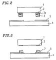
- the adhesive layers 3 of the thermoplastic conductive adhesive are directly formed on the terminal electrodes 2 of the semiconductor device 1 .
- the adhesive layers 3 can also be formed as follows: As shown in Figure 2 , a bump electrode 2a is formed on each terminal electrode 2 , after which an adhesive layer 3 is formed on each of the thus formed bump electrodes 2a .
- the height of the bump electrodes 2a is preferably set such that the distance of the gap between the semiconductor device 1 and the circuit board 4 is in the range of 20 ⁇ m to 100 ⁇ m. If the gap is smaller than 20 ⁇ m, it is difficult to fill the gap with sealing resin. If the gap is larger than 100 ⁇ m, it is difficult to form the bump electrodes 2a .
- adhesive layers 3 can be formed directly on the connecting electrodes 5 of the circuit board 4 .
- the same steps as those of the above-described embodiment shown in Figures 1B to 1D are performed, so that a highly reliable circuit board with a semiconductor device mounted thereon can be obtained.
- the cured resin layer 9 is formed only in a gap between the semiconductor device 1 and the circuit board 4 .
- the present invention is not limited to this construction, the resin layer 9 may cover the peripheral portions of the semiconductor device 1 also, as shown in Figure 4 .
- thermoplastic conductive adhesive used in the present invention can be any thermoplastic conductive adhesive made of a thermoplastic resin such as a polyester resin containing a conductive filler such as Ag or the like. It can further contain an organic solvent.
- thermosetting resin used in the present invention can be any insulating resin, such as an epoxy resin, a silicone resin, a polyimide resin or a phenol resin, curable at temperatures equal to or higher than the plasticizing temperature of the thermoplastic conductive adhesive. Furthermore, an inorganic filler such as silica can be added to the thermosetting resin, thereby reducing its coefficient of thermal expansion. Using this thermosetting resin with a reduced coefficient of thermal expansion, the reliability of the connection between the semiconductor device and the circuit board can be further increased.
Landscapes
- Wire Bonding (AREA)
Applications Claiming Priority (9)
| Application Number | Priority Date | Filing Date | Title |
|---|---|---|---|
| JP5242647A JP2548891B2 (ja) | 1993-09-29 | 1993-09-29 | 半導体装置の実装方法とその実装体 |
| JP5242645A JP2721789B2 (ja) | 1993-09-29 | 1993-09-29 | 半導体装置の封止方法 |
| JP24264693 | 1993-09-29 | ||
| JP242647/93 | 1993-09-29 | ||
| JP24264793 | 1993-09-29 | ||
| JP242646/93 | 1993-09-29 | ||
| JP242645/93 | 1993-09-29 | ||
| JP24264593 | 1993-09-29 | ||
| JP5242646A JP2721790B2 (ja) | 1993-09-29 | 1993-09-29 | 半導体装置の封止方法 |
Publications (3)
| Publication Number | Publication Date |
|---|---|
| EP0645805A2 EP0645805A2 (en) | 1995-03-29 |
| EP0645805A3 EP0645805A3 (OSRAM) | 1995-04-12 |
| EP0645805B1 true EP0645805B1 (en) | 2000-11-29 |
Family
ID=27333060
Family Applications (1)
| Application Number | Title | Priority Date | Filing Date |
|---|---|---|---|
| EP94115187A Expired - Lifetime EP0645805B1 (en) | 1993-09-29 | 1994-09-27 | Method for mounting a semiconductor device on a circuit board, and a circuit board with a semiconductor device mounted thereon |
Country Status (4)
| Country | Link |
|---|---|
| US (2) | US5670826A (OSRAM) |
| EP (1) | EP0645805B1 (OSRAM) |
| KR (1) | KR0171438B1 (OSRAM) |
| DE (1) | DE69426347T2 (OSRAM) |
Families Citing this family (47)
| Publication number | Priority date | Publication date | Assignee | Title |
|---|---|---|---|---|
| US5376561A (en) * | 1990-12-31 | 1994-12-27 | Kopin Corporation | High density electronic circuit modules |
| JP3534501B2 (ja) * | 1995-08-25 | 2004-06-07 | 株式会社ルネサステクノロジ | 半導体装置の製造方法 |
| US6159770A (en) * | 1995-11-08 | 2000-12-12 | Fujitsu Limited | Method and apparatus for fabricating semiconductor device |
| US6072239A (en) | 1995-11-08 | 2000-06-06 | Fujitsu Limited | Device having resin package with projections |
| US6376921B1 (en) | 1995-11-08 | 2002-04-23 | Fujitsu Limited | Semiconductor device, method for fabricating the semiconductor device, lead frame and method for producing the lead frame |
| US6329711B1 (en) | 1995-11-08 | 2001-12-11 | Fujitsu Limited | Semiconductor device and mounting structure |
| JP2951882B2 (ja) | 1996-03-06 | 1999-09-20 | 松下電器産業株式会社 | 半導体装置の製造方法及びこれを用いて製造した半導体装置 |
| JP3409957B2 (ja) * | 1996-03-06 | 2003-05-26 | 松下電器産業株式会社 | 半導体ユニット及びその形成方法 |
| JP2828021B2 (ja) * | 1996-04-22 | 1998-11-25 | 日本電気株式会社 | ベアチップ実装構造及び製造方法 |
| US5808874A (en) | 1996-05-02 | 1998-09-15 | Tessera, Inc. | Microelectronic connections with liquid conductive elements |
| US5918363A (en) * | 1996-05-20 | 1999-07-06 | Motorola, Inc. | Method for marking functional integrated circuit chips with underfill material |
| JP3201957B2 (ja) * | 1996-06-27 | 2001-08-27 | インターナショナル・ビジネス・マシーンズ・コーポレーション | 金属バンプ、金属バンプの製造方法、接続構造体 |
| US6020220A (en) * | 1996-07-09 | 2000-02-01 | Tessera, Inc. | Compliant semiconductor chip assemblies and methods of making same |
| JPH1041694A (ja) * | 1996-07-25 | 1998-02-13 | Sharp Corp | 半導体素子の基板実装構造及びその実装方法 |
| JP3431406B2 (ja) * | 1996-07-30 | 2003-07-28 | 株式会社東芝 | 半導体パッケージ装置 |
| DE19639934A1 (de) * | 1996-09-27 | 1998-04-09 | Siemens Ag | Verfahren zur Flipchip-Kontaktierung eines Halbleiterchips mit geringer Anschlußzahl |
| JP2924830B2 (ja) * | 1996-11-15 | 1999-07-26 | 日本電気株式会社 | 半導体装置及びその製造方法 |
| JPH10214925A (ja) * | 1996-11-28 | 1998-08-11 | Nitto Denko Corp | 半導体素子封止用封止ラベル |
| US6635514B1 (en) | 1996-12-12 | 2003-10-21 | Tessera, Inc. | Compliant package with conductive elastomeric posts |
| US6417029B1 (en) | 1996-12-12 | 2002-07-09 | Tessera, Inc. | Compliant package with conductive elastomeric posts |
| KR100384314B1 (ko) * | 1996-12-27 | 2003-05-16 | 마츠시타 덴끼 산교 가부시키가이샤 | 회로기판에의 전자부품 실장방법 및 장치 |
| JPH1126631A (ja) * | 1997-07-02 | 1999-01-29 | Matsushita Electric Ind Co Ltd | 半導体装置とその製造方法 |
| US6228206B1 (en) * | 1997-07-30 | 2001-05-08 | Drug Delivery Technologies, Inc. | Bonding agent composition containing conductive filler and method of bonding electrode to printed conductive trace with same |
| EP1194030B1 (en) * | 1997-10-02 | 2005-08-03 | Matsushita Electric Industrial Co., Ltd. | Method for mounting semiconductor element to circuit board, and semiconductor device |
| US6038133A (en) * | 1997-11-25 | 2000-03-14 | Matsushita Electric Industrial Co., Ltd. | Circuit component built-in module and method for producing the same |
| JPH11163501A (ja) * | 1997-12-02 | 1999-06-18 | Rohm Co Ltd | 電子部品の実装方法、およびその方法によって製造された電子回路装置 |
| FR2773642B1 (fr) * | 1998-01-13 | 2000-03-03 | Schlumberger Ind Sa | Procede de connexion de plots d'un composant a circuits integres a des plages de connexion d'un substrat plastique au moyen de protuberances |
| JP3834424B2 (ja) * | 1998-05-29 | 2006-10-18 | 株式会社東芝 | 半導体装置 |
| JP3692935B2 (ja) * | 1998-07-01 | 2005-09-07 | セイコーエプソン株式会社 | 半導体装置の製造方法 |
| AU4802199A (en) * | 1998-07-28 | 2000-02-21 | Hitachi Chemical Company, Ltd. | Semiconductor device and method for manufacturing the same |
| US6224711B1 (en) | 1998-08-25 | 2001-05-01 | International Business Machines Corporation | Assembly process for flip chip package having a low stress chip and resulting structure |
| JP3982932B2 (ja) * | 1998-12-11 | 2007-09-26 | 株式会社沖データ | Ledアレイヘッド |
| JP3459787B2 (ja) * | 1999-04-02 | 2003-10-27 | Nec化合物デバイス株式会社 | 光半導体モジュール及びその製造方法 |
| US6376051B1 (en) | 1999-03-10 | 2002-04-23 | Matsushita Electric Industrial Co., Ltd. | Mounting structure for an electronic component and method for producing the same |
| JP3423897B2 (ja) * | 1999-04-01 | 2003-07-07 | 宮崎沖電気株式会社 | 半導体装置の製造方法 |
| US6544880B1 (en) * | 1999-06-14 | 2003-04-08 | Micron Technology, Inc. | Method of improving copper interconnects of semiconductor devices for bonding |
| AU2001244016A1 (en) * | 2000-03-31 | 2001-10-15 | Dyconex Patente Ag | Method for fabricating electrical connecting elements, and connecting element |
| US7547579B1 (en) * | 2000-04-06 | 2009-06-16 | Micron Technology, Inc. | Underfill process |
| US6512183B2 (en) * | 2000-10-10 | 2003-01-28 | Matsushita Electric Industrial Co., Ltd. | Electronic component mounted member and repair method thereof |
| JP2003152021A (ja) * | 2001-11-09 | 2003-05-23 | Seiko Epson Corp | 半導体装置及びその製造方法、回路基板並びに電子機器 |
| US7645262B2 (en) | 2002-04-11 | 2010-01-12 | Second Sight Medical Products, Inc. | Biocompatible bonding method and electronics package suitable for implantation |
| US20040161220A1 (en) * | 2002-09-09 | 2004-08-19 | Adc Telecommunications, Inc. | Method for face-mounting optical components and devices using same |
| US7047633B2 (en) * | 2003-05-23 | 2006-05-23 | National Starch And Chemical Investment Holding, Corporation | Method of using pre-applied underfill encapsulant |
| US7239016B2 (en) * | 2003-10-09 | 2007-07-03 | Denso Corporation | Semiconductor device having heat radiation plate and bonding member |
| DE102009058435A1 (de) * | 2009-12-16 | 2011-06-22 | Giesecke & Devrient GmbH, 81677 | Befestigen und elektrisch leitendes Verbinden eines Chipmoduls mit einer Chipkarte |
| US9064820B2 (en) | 2012-04-05 | 2015-06-23 | Mekiec Manufacturing Corporation (Thailand) Ltd | Method and encapsulant for flip-chip assembly |
| WO2019171523A1 (ja) * | 2018-03-08 | 2019-09-12 | 三菱電機株式会社 | 半導体素子、半導体装置、電力変換装置、及び、半導体素子の製造方法 |
Citations (2)
| Publication number | Priority date | Publication date | Assignee | Title |
|---|---|---|---|---|
| JPH05218137A (ja) * | 1992-02-05 | 1993-08-27 | Toshiba Corp | 半導体装置の製造方法 |
| US5360942A (en) * | 1993-11-16 | 1994-11-01 | Olin Corporation | Multi-chip electronic package module utilizing an adhesive sheet |
Family Cites Families (14)
| Publication number | Priority date | Publication date | Assignee | Title |
|---|---|---|---|---|
| US3795047A (en) * | 1972-06-15 | 1974-03-05 | Ibm | Electrical interconnect structuring for laminate assemblies and fabricating methods therefor |
| JPS5357481A (en) * | 1976-11-04 | 1978-05-24 | Canon Inc | Connecting process |
| JPS54105774A (en) * | 1978-02-08 | 1979-08-20 | Hitachi Ltd | Method of forming pattern on thin film hybrid integrated circuit |
| CN87107692A (zh) * | 1986-11-13 | 1988-05-25 | Mt化学公司 | 半导体器件的制造方法 |
| JPS63249393A (ja) * | 1987-04-03 | 1988-10-17 | シャープ株式会社 | 電子部品の接続方法 |
| US4917466A (en) * | 1987-08-13 | 1990-04-17 | Shin-Etsu Polymer Co., Ltd. | Method for electrically connecting IC chips, a resinous bump-forming composition used therein and a liquid-crystal display unit electrically connected thereby |
| JPS6472547A (en) * | 1987-09-12 | 1989-03-17 | Oki Electric Ind Co Ltd | Semiconductor device and manufacture thereof |
| JP2596960B2 (ja) * | 1988-03-07 | 1997-04-02 | シャープ株式会社 | 接続構造 |
| US5121190A (en) * | 1990-03-14 | 1992-06-09 | International Business Machines Corp. | Solder interconnection structure on organic substrates |
| JP2843658B2 (ja) * | 1990-08-02 | 1999-01-06 | 東レ・ダウコーニング・シリコーン株式会社 | フリップチップ型半導体装置 |
| JP2940269B2 (ja) * | 1990-12-26 | 1999-08-25 | 日本電気株式会社 | 集積回路素子の接続方法 |
| JP2699726B2 (ja) * | 1991-11-15 | 1998-01-19 | 松下電器産業株式会社 | 半導体装置の実装方法 |
| US5318651A (en) * | 1991-11-27 | 1994-06-07 | Nec Corporation | Method of bonding circuit boards |
| US5412867A (en) * | 1992-05-25 | 1995-05-09 | Matsushita Electric Industrial Co., Ltd. | Method of joining flat electrodes |
-
1994
- 1994-09-27 KR KR1019940024239A patent/KR0171438B1/ko not_active Expired - Fee Related
- 1994-09-27 DE DE69426347T patent/DE69426347T2/de not_active Expired - Lifetime
- 1994-09-27 EP EP94115187A patent/EP0645805B1/en not_active Expired - Lifetime
-
1996
- 1996-09-09 US US08/709,606 patent/US5670826A/en not_active Expired - Lifetime
- 1996-10-15 US US08/731,521 patent/US5651179A/en not_active Expired - Lifetime
Patent Citations (2)
| Publication number | Priority date | Publication date | Assignee | Title |
|---|---|---|---|---|
| JPH05218137A (ja) * | 1992-02-05 | 1993-08-27 | Toshiba Corp | 半導体装置の製造方法 |
| US5360942A (en) * | 1993-11-16 | 1994-11-01 | Olin Corporation | Multi-chip electronic package module utilizing an adhesive sheet |
Non-Patent Citations (2)
| Title |
|---|
| Hawley's condensed Chemical Dictionary, pub. Van Nostrand '87, pg. 467 * |
| PATENT ABSTRACTS OF JAPAN vol. 017, no. 657 (E - 1470) 6 December 1993 (1993-12-06) * |
Also Published As
| Publication number | Publication date |
|---|---|
| DE69426347T2 (de) | 2001-05-17 |
| KR0171438B1 (ko) | 1999-10-15 |
| US5651179A (en) | 1997-07-29 |
| EP0645805A3 (OSRAM) | 1995-04-12 |
| EP0645805A2 (en) | 1995-03-29 |
| US5670826A (en) | 1997-09-23 |
| DE69426347D1 (de) | 2001-01-04 |
Similar Documents
| Publication | Publication Date | Title |
|---|---|---|
| EP0645805B1 (en) | Method for mounting a semiconductor device on a circuit board, and a circuit board with a semiconductor device mounted thereon | |
| US6175159B1 (en) | Semiconductor package | |
| US5677575A (en) | Semiconductor package having semiconductor chip mounted on board in face-down relation | |
| KR100256293B1 (ko) | 반도체장치 및 그 제조방법 | |
| EP1043771B1 (en) | Method of fabricating a resin sealed electronic device | |
| KR100336329B1 (ko) | 반도체장치의제조방법 | |
| KR100352865B1 (ko) | 반도체 장치 및 그 제조방법 | |
| KR20000005915A (ko) | 반도체장치와그제조방법 | |
| US6661099B2 (en) | Semiconductor device, semiconductor package for use therein, and manufacturing method thereof | |
| US6894384B1 (en) | Semiconductor device and method of manufacturing the same | |
| JPH06334070A (ja) | 混成集積回路装置 | |
| JP2705658B2 (ja) | 電子デバイス組立体およびその製造方法 | |
| JP2637684B2 (ja) | 半導体装置の封止方法 | |
| JP2721790B2 (ja) | 半導体装置の封止方法 | |
| JP2548891B2 (ja) | 半導体装置の実装方法とその実装体 | |
| JP3045940B2 (ja) | 半導体装置およびその製造方法 | |
| JP2721789B2 (ja) | 半導体装置の封止方法 | |
| JP2752286B2 (ja) | 混成集積回路装置 | |
| JPH06232208A (ja) | 半導体装置の封止方法と封止構造 | |
| JPH06232207A (ja) | 半導体装置の封止方法と封止構造 | |
| JP2678111B2 (ja) | 半導体装置の取り外し方法 | |
| JPH01187833A (ja) | 半導体装置 | |
| JPH05121593A (ja) | 混成集積回路 | |
| KR20010017144A (ko) | 적층형 플립 칩 패키지용 캐리어 테이프 제조방법 | |
| JPS61109026A (ja) | 液晶表示素子 |
Legal Events
| Date | Code | Title | Description |
|---|---|---|---|
| PUAI | Public reference made under article 153(3) epc to a published international application that has entered the european phase |
Free format text: ORIGINAL CODE: 0009012 |
|
| PUAL | Search report despatched |
Free format text: ORIGINAL CODE: 0009013 |
|
| 17P | Request for examination filed |
Effective date: 19940928 |
|
| AK | Designated contracting states |
Kind code of ref document: A2 Designated state(s): DE FR GB NL |
|
| AK | Designated contracting states |
Kind code of ref document: A3 Designated state(s): DE FR GB NL |
|
| RAP1 | Party data changed (applicant data changed or rights of an application transferred) |
Owner name: MATSUSHITA ELECTRIC INDUSTRIAL CO., LTD. |
|
| K1C1 | Correction of patent application (title page) published |
Effective date: 19950329 |
|
| 17Q | First examination report despatched |
Effective date: 19951208 |
|
| GRAG | Despatch of communication of intention to grant |
Free format text: ORIGINAL CODE: EPIDOS AGRA |
|
| GRAG | Despatch of communication of intention to grant |
Free format text: ORIGINAL CODE: EPIDOS AGRA |
|
| GRAH | Despatch of communication of intention to grant a patent |
Free format text: ORIGINAL CODE: EPIDOS IGRA |
|
| GRAH | Despatch of communication of intention to grant a patent |
Free format text: ORIGINAL CODE: EPIDOS IGRA |
|
| GRAA | (expected) grant |
Free format text: ORIGINAL CODE: 0009210 |
|
| AK | Designated contracting states |
Kind code of ref document: B1 Designated state(s): DE FR GB NL |
|
| REF | Corresponds to: |
Ref document number: 69426347 Country of ref document: DE Date of ref document: 20010104 |
|
| ET | Fr: translation filed | ||
| PLBE | No opposition filed within time limit |
Free format text: ORIGINAL CODE: 0009261 |
|
| STAA | Information on the status of an ep patent application or granted ep patent |
Free format text: STATUS: NO OPPOSITION FILED WITHIN TIME LIMIT |
|
| 26N | No opposition filed | ||
| REG | Reference to a national code |
Ref country code: GB Ref legal event code: IF02 |
|
| PGFP | Annual fee paid to national office [announced via postgrant information from national office to epo] |
Ref country code: FR Payment date: 20100921 Year of fee payment: 17 |
|
| PGFP | Annual fee paid to national office [announced via postgrant information from national office to epo] |
Ref country code: GB Payment date: 20100922 Year of fee payment: 17 |
|
| PGFP | Annual fee paid to national office [announced via postgrant information from national office to epo] |
Ref country code: NL Payment date: 20100916 Year of fee payment: 17 |
|
| PGFP | Annual fee paid to national office [announced via postgrant information from national office to epo] |
Ref country code: DE Payment date: 20100922 Year of fee payment: 17 |
|
| REG | Reference to a national code |
Ref country code: NL Ref legal event code: V1 Effective date: 20120401 |
|
| GBPC | Gb: european patent ceased through non-payment of renewal fee |
Effective date: 20110927 |
|
| REG | Reference to a national code |
Ref country code: FR Ref legal event code: ST Effective date: 20120531 |
|
| REG | Reference to a national code |
Ref country code: DE Ref legal event code: R119 Ref document number: 69426347 Country of ref document: DE Effective date: 20120403 |
|
| PG25 | Lapsed in a contracting state [announced via postgrant information from national office to epo] |
Ref country code: NL Free format text: LAPSE BECAUSE OF NON-PAYMENT OF DUE FEES Effective date: 20120401 Ref country code: DE Free format text: LAPSE BECAUSE OF NON-PAYMENT OF DUE FEES Effective date: 20120403 |
|
| PG25 | Lapsed in a contracting state [announced via postgrant information from national office to epo] |
Ref country code: FR Free format text: LAPSE BECAUSE OF NON-PAYMENT OF DUE FEES Effective date: 20110930 Ref country code: GB Free format text: LAPSE BECAUSE OF NON-PAYMENT OF DUE FEES Effective date: 20110927 |