EP0569716B1 - Entschachtelungsschaltung zum Regenerieren von digitalen Daten - Google Patents
Entschachtelungsschaltung zum Regenerieren von digitalen Daten Download PDFInfo
- Publication number
- EP0569716B1 EP0569716B1 EP93105966A EP93105966A EP0569716B1 EP 0569716 B1 EP0569716 B1 EP 0569716B1 EP 93105966 A EP93105966 A EP 93105966A EP 93105966 A EP93105966 A EP 93105966A EP 0569716 B1 EP0569716 B1 EP 0569716B1
- Authority
- EP
- European Patent Office
- Prior art keywords
- data
- circuit
- pointer
- error
- error correcting
- Prior art date
- Legal status (The legal status is an assumption and is not a legal conclusion. Google has not performed a legal analysis and makes no representation as to the accuracy of the status listed.)
- Expired - Lifetime
Links
Images


Classifications
-
- G—PHYSICS
- G11—INFORMATION STORAGE
- G11B—INFORMATION STORAGE BASED ON RELATIVE MOVEMENT BETWEEN RECORD CARRIER AND TRANSDUCER
- G11B20/00—Signal processing not specific to the method of recording or reproducing; Circuits therefor
- G11B20/10—Digital recording or reproducing
-
- G—PHYSICS
- G11—INFORMATION STORAGE
- G11B—INFORMATION STORAGE BASED ON RELATIVE MOVEMENT BETWEEN RECORD CARRIER AND TRANSDUCER
- G11B20/00—Signal processing not specific to the method of recording or reproducing; Circuits therefor
- G11B20/10—Digital recording or reproducing
- G11B20/18—Error detection or correction; Testing, e.g. of drop-outs
- G11B20/1806—Pulse code modulation systems for audio signals
- G11B20/1809—Pulse code modulation systems for audio signals by interleaving
-
- H—ELECTRICITY
- H03—ELECTRONIC CIRCUITRY
- H03M—CODING; DECODING; CODE CONVERSION IN GENERAL
- H03M13/00—Coding, decoding or code conversion, for error detection or error correction; Coding theory basic assumptions; Coding bounds; Error probability evaluation methods; Channel models; Simulation or testing of codes
- H03M13/27—Coding, decoding or code conversion, for error detection or error correction; Coding theory basic assumptions; Coding bounds; Error probability evaluation methods; Channel models; Simulation or testing of codes using interleaving techniques
Definitions
- the present invention relates to a de-interleave circuit for regenerating digital data in a digital data regenerating apparatus in accordance with the precharacterizing part of claim 1.
- a de-interleave circuit of said kind is known from EP-A-86 566.
- CD Compact disks
- MD minidisk
- the MD player is employing a magnetooptic recording system. Further, the interleave method used in the MD system is adapted to facilitate "waveform joining" and provide an interleave effect to that obtainable in the CD system.
- FIG. 9 The sequence of de-interleave in the MD system is shown in FIG. 9. On the left of FIG. 9, there are shown the data for 1 frame regenerated from the disk. The data regenerated at the start of the frame following the subcode is the 8-bit data W12 n , A. The data generated next is the data W12 n , B.
- n the frame number
- P n the C1 parity
- Q n the C2 parity
- the C1 correction is applied to the data W12 n , A, W12 n , B obtained 1 frame before, W12 n+1 , A, W12 n+1 , B obtained 1 frame before, ... , in order of mention and one coded word is provided by the data of 32 bytes.
- C1 flags C1 pointers
- the RAM used is that having a data width of 8 bits, only 1 bit out of them is used as the C1 flag.
- the C2 correction is applied to the data W12 n , A obtained 108 frames before, W12 n , B obtained 105 frames before, ... , in order of mention and one coded word is provided by the data of 28 bytes.
- the C1 flag is utilized for calculation of the C2 error correction to thereby prevent false correction or utilized for erasure correction.
- the C1 flag of each data is used. More specifically, when there is set up a C1 flag, a C2 pointer (C2 flag) is set up as the error data.
- the C2 pointer is attached to each 8-bit data to be paired therewith.
- the apparatus for error correction and the de-interleave circuit known from EP-A-86 566 is directed to simultaneously or parallelly execute an error correction and pointer setting by a microprogram stored in a memory. Said parallel operations are improving the efficiency of the calculation processing needed for error correction.
- the known apparatus is not designed to operate in a number of different operating modes such as MD and CD with the same microprogram and not to reduce the capacity of a buffer memory.
- the present invention has been made in view of the above described problem and it is an object of the present invention to provide a de-interleave circuit which is applicable to de-interleaving in the MD system, while it is realized with the use of a 32K-bit buffer RAM, and, in addition, capable of using the error correcting program in common with the CD system.
- a de-interleave circuit for regenerating digital data in a digital data regenerating apparatus which receives errors in the data which is formed of a predetermined number of words corresponding to one frame and encoded in a C1 and C2 error code in parallel, the error code word being interleaved in a plurality of frames, the circuit comprising
- a de-interleave circuit is arranged such that C2 error correcting flags in one word are correspondingly set up for the data of a corresponding number of words and the number of error correchting flags assembled for said corresponding number of data words are made different in the CD mode and in the MD mode, and thus error correction is made possible by using a common microprogram in both modes, and the capacity for the C2 error correcting flags (C2 pointers) in the C2 correction in the MD mode is made smaller than in the CD mode.
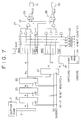
- FIG. 1 is a block diagram showing the arrangement of a circuit for regenerating digital data to which a de-interleave circuit according to the present invention is applied.
- an EFM signal read from an MD is EFM demodulated in an EFM demodulator circuit 1.
- PCM audio data as the demodulated output i.e., data of 8 bits (one symbol in parallel) is recorded in a buffer RAM 3 of 32K bits through an external bus 2.
- the RAM 3 functions as a buffer for de-interleaving the CIRC (Cross Interleave Read Solomon Code) and the related error connection.
- CIRC Cross Interleave Read Solomon Code
- the de-interleaved C1 and C2 data of 32 symbols and 28 symbols, respectively, are input through an input circuit 4 to be supplied to an error correcting circuit 6 through an internal bus 5.
- the sequence of the data in this stage is as shown in FIG. 9.
- C2 error correcting flags herein called C2 pointers are set up for uncorrected information.
- C1 pointers are copied.
- C2 pointers are established for the whole of the C2 information (hereinafter called "all pointer").
- a C2 flag or pointer setting circuit 7 and a flag or pointer processing circuit 8 are provided, each being connected to the internal bus 5.
- the C2 pointer setting circuit 7 and the pointer processing circuit 8 are adapted to be controlled by a microprogram sequencer 9.
- pointers "1" for all of the 8 bits are set by the C2 pointer setting circuit 7 in the internal bus 5 upon issuance of the C2 pointer setting instruction from the microprogram sequencer 9 and then the pointers are set, through an output circuit 10, in the external bus (data bus) 2 connected with the RAM 3.
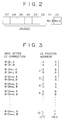
- C2 pointers are written 12 times for the data of 24 bytes in the CD mode as shown in FIG. 3, C2 pointers are written at the same address four times over in the MD mode. Therefore, the microprogram can be used in common.
- the C1 pointer is copied as the C2 pointer if the C1 correction is considered to have been correctly made.
- the pointer processing circuit 8 When the copying instruction is issued from the microprogram sequencer 9, the pointer processing circuit 8 operates under a C1 pointer read instruction and a C2 pointer write instruction issued by the microprogram sequencer 9.
- the pointer processing circuit 8 there are connected in series 8-bit D-FF (flip-flops) 11 1 to 11 8 with the enable terminal (E) as shown in FIG. 4.
- the D-FF 11 1 to 11 8 use the C1 pointer read instruction as the enable input.
- the flip-flop D-FF 11 1 in the first stage receives the LSB (least significant bit) of the C1 pointer supplied from the internal bus 5 as the data (D) input.
- the C1 pointer is written only in the LSB.
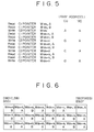
- the microprogram at the pointer copying portion in the CD mode is as shown in FIG. 5. More specifically, the operation reading the C1 pointer two times and writing the C2 pointer one time is repeated.
- a C2 pointer arranged in 8 bits is first recorded as a set of the data in the RAM. Namely, 1 byte of the C2 pointer is assigned to the 8 bytes of the data W12 n , A to W12 n+3 , B. The C2 pointer remains recorded in the RAM 3 for a period of 7D.
- the total capacity of the buffer RAM 3, in contrast to (1) to (3) above, becomes 48 + 1,620 + 1,296 + 12 + 212 3,188 bytes.
- PCM audio information after error correction, is supplied to a D/A interface circuit 13 through the external bus 2 and subjected, therein, to interpolation, parallel/serial conversion, and so on.
- a data request processing circuit 14 is provided for receiving requests from several reading/writing circuits for allocation of storage location of the buffer RAM 3. More specifically, when the error correcting circuit 6 uses the buffer RAM 3, the error correcting circuit 6 outputs the request to the data request processing circuit 14. Other than that, write requests or read requests from the D/A interface circuit 13 and the EFM demodulator circuit 1 are input to the data request processing circuit 14. When two or more requests arrive simultaneously, one out of them is accepted according to predetermined priority. Then, at the request, an address generator circuit 15 generates a real address in the buffer RAM 3.
- the D/A interface circuit 13 Since the data for which a C2 pointer is set up is error data which has not been corrected even by the C2 correction, the D/A interface circuit 13 performs such operation as interpolation, namely, it obtains and outputs the average value of the correct data before and after the error data.
- a C2 pointer and the data which has undergone error correction after de-interleaving are placed while a timing pulse DABSRE is at high level.
- the timing pulse DABSRE has four pulses in a set as shown in FIG. 8, and the pointer P L (low order), pointer P U (high order), data W X , B (low order), and data W X , A (high order) are placed on the data bus 2 in order of mention in accordance with the four pulses.
- the above data are stored into four 8-bit registers 21 to 24 having the timing pulse DABSRE as the enable (E) input.
- the register 21 functions as that for the low-order pointer P L and the register 22 functions as that for the high-order pointer P U .
- a 4-bit counter 25 making a counting operation in synchronism with the fall of the timing pulse DABSRE.
- This counter 25 loads (0, 0, 0, 0) therein responding to the timing pulse XRFCKRS generated at the head of the frame. Relationships between the count value of the counter 25 and the timing pulse DABSRE are shown in the timing chart of FIG. 8.
- the pointer corresponding to the 2-byte data is selected according to the count value of the counter 25 from among the 8-bit C2 pointers stored in the registers 21 and 22.
- the low-order pointer P L selected from the C2 pointers in the register 21 is passed through a gate circuit 28 and latched by a latch circuit 30, while the high-order pointer P U selected from the C2 pointers in the register 22 is passed through a gate circuit 29 and latched by a latch circuit 31.
- the timing pulse DABSRE has three pulses in a set and the low-order 2 bits of the C2 pointer stored in the register 22 can be obtained by means of the gate circuit 29 as the pointer in common for the data W X , A/W X , B.
- the content of the C2 pointer is checked in the D/A interface circuit 13. Since the data with a C2 pointer set up therefor is error data, it is subjected to interpolation or other treatment.
- the capacity for the C2 pointers can be decreased to 1/4 of that in the CD player where 1 byte for the C2 pointer was required for 2-byte data. Therefore, it becomes possible to realize a de-interleave circuit using 32K-bit RAM.
Landscapes
- Engineering & Computer Science (AREA)
- Signal Processing (AREA)
- Multimedia (AREA)
- Physics & Mathematics (AREA)
- Probability & Statistics with Applications (AREA)
- Theoretical Computer Science (AREA)
- Error Detection And Correction (AREA)
- Detection And Correction Of Errors (AREA)
- Signal Processing For Digital Recording And Reproducing (AREA)
Claims (2)
- Entschachtelungsschaltung zum Regenerieren von digitalen Daten in einem digitalen Datenregeneriergerät, das Fehler in den Daten empfängt, die aus einer vorbestimmten Anzahl von Worten entsprechend einem Rahmen gebildet und in einem C1- und C2-Fehlercode parallel codiert sind, wobei das Fehlercodewort in einer Vielzahl von Rahmen verschachtelt ist, wobei die Schaltung aufweist:dadurch gekennzeichnet, daßeine Demodulatorschaltung (1) zum Demodulieren von Digitaldaten,einen Puffer-RAM (3) zum Zwischenspeichern von demodulierten Daten und von Flag-Daten, von denen eine Fehlerkorrektur und Ausgabe ausgeführt werden,eine Fehlerkorrekturschaltung (6), die Daten von dem Puffer-RAM (3) über eine Eingabeschaltung empfängt und eine Fehlerkorrektur der empfangenen Daten ausführt,einen Mikroprogramm-Sequenzer (9), undeine C2-Flag-Setzschaltung (7), die durch den Mikroprogramm-Sequenzer (9) gesteuert ist,die Fehlerkorrekturschaltung (6) Fehler in den parallel empfangenen Daten durch Ansammeln von C2-Fehler-Korrektur-Flags in einem Wort korrigiert, wobei jede Fehler-Korrektur-Flag innerhalb eines Wortes ein jeweiliges Datenwort innerhalb einer entsprechenden Anzahl von Datenwörtern (W12n,A - W12n+3,B; W12n+4,A - W12n+7,B; W12n+8,A - W12n+11,B) darstellt und die C2-Flag-Setzschaltung (7) und eine Flag-Verarbeitungsschaltung (8), gesteuert durch den Mikroprogramm-Sequenzer (9) C2-Fehler-Korrekturflags aufbauen, während die Anzahl der für die entsprechende Anzahl von Datenwörtern angesammelten C2-Fehler-Korrektur-Flags verschieden gemacht ist in jeder einer Vielzahl von verschiedenen Betriebsarten (MD, CD-Modus).
- Entschachtelungsschaltung nach Anspruch 1, bei der die Fehlerkorrekturschaltung (6) eine Fehlerkorrektur mittels eines gemeinsamen Mikroprogrammes in der Vielzahl von verschiedenen Betriebsarten ausführt.
Applications Claiming Priority (2)
| Application Number | Priority Date | Filing Date | Title |
|---|---|---|---|
| JP11979892A JP3259323B2 (ja) | 1992-04-13 | 1992-04-13 | デ・インターリーブ回路 |
| JP119798/92 | 1992-04-13 |
Publications (3)
| Publication Number | Publication Date |
|---|---|
| EP0569716A2 EP0569716A2 (de) | 1993-11-18 |
| EP0569716A3 EP0569716A3 (en) | 1994-07-27 |
| EP0569716B1 true EP0569716B1 (de) | 1998-06-17 |
Family
ID=14770493
Family Applications (1)
| Application Number | Title | Priority Date | Filing Date |
|---|---|---|---|
| EP93105966A Expired - Lifetime EP0569716B1 (de) | 1992-04-13 | 1993-04-13 | Entschachtelungsschaltung zum Regenerieren von digitalen Daten |
Country Status (5)
| Country | Link |
|---|---|
| US (1) | US5528608A (de) |
| EP (1) | EP0569716B1 (de) |
| JP (1) | JP3259323B2 (de) |
| KR (1) | KR100259435B1 (de) |
| DE (1) | DE69319181T2 (de) |
Families Citing this family (67)
| Publication number | Priority date | Publication date | Assignee | Title |
|---|---|---|---|---|
| KR100211830B1 (ko) * | 1995-03-16 | 1999-08-02 | 윤종용 | 미니디스크의 적응변환 오디오 코딩회로 |
| WO1996037050A1 (en) * | 1995-05-15 | 1996-11-21 | Advanced Hardware Architectures, Inc. | Reconfigurable interleaver/deinterleaver and address generator for data streams interleaved according to one of a plurality of interleaving schemes |
| TW301740B (de) * | 1995-05-31 | 1997-04-01 | Sony Co Ltd | |
| US5793724A (en) * | 1996-01-22 | 1998-08-11 | Sony Corporation | Optical disk error-correcting code system correlating error correction with sector address |
| GB2329508B (en) * | 1997-06-28 | 2000-01-12 | United Microelectronics Corp | Controller circuit apparatus for cd-rom drives |
| TW334533B (en) * | 1997-06-28 | 1998-06-21 | United Microelectronics Corp | The control circuit apparatus for CD-ROM optical disk driver |
| US6298085B1 (en) | 1997-10-23 | 2001-10-02 | Sony Corporation | Source encoding using shuffling of data to provide robust error recovery in a burst error-environment |
| US6581170B1 (en) | 1997-10-23 | 2003-06-17 | Sony Corporation | Source coding to provide for robust error recovery during transmission losses |
| NL1007427C2 (nl) * | 1997-11-03 | 1999-05-04 | United Microelectronics Corp | Stuurschakelingsinrichting voor CD-ROM-aandrijfmechanismen. |
| US6519369B1 (en) | 1999-02-12 | 2003-02-11 | Sony Corporation | Method and apparatus for filter tap expansion |
| US6307979B1 (en) | 1999-02-12 | 2001-10-23 | Sony Corporation | Classified adaptive error recovery method and apparatus |
| US6170074B1 (en) | 1999-02-12 | 2001-01-02 | Sony Corporation | Source coding to provide for robust error recovery |
| US6151416A (en) * | 1999-02-12 | 2000-11-21 | Sony Corporation | Method and apparatus for adaptive class tap selection according to multiple classification |
| US6591398B1 (en) | 1999-02-12 | 2003-07-08 | Sony Corporation | Multiple processing system |
| US6535148B1 (en) | 1999-02-12 | 2003-03-18 | Sony Corporation | Method and apparatus for truncated decoding |
| US6192161B1 (en) | 1999-02-12 | 2001-02-20 | Sony Corporation | Method and apparatus for adaptive filter tap selection according to a class |
| US6154761A (en) * | 1999-02-12 | 2000-11-28 | Sony Corporation | Classified adaptive multiple processing system |
| US6621936B1 (en) | 1999-02-12 | 2003-09-16 | Sony Corporation | Method and apparatus for spatial class reduction |
| US7730300B2 (en) | 1999-03-30 | 2010-06-01 | Sony Corporation | Method and apparatus for protecting the transfer of data |
| US7565546B2 (en) | 1999-03-30 | 2009-07-21 | Sony Corporation | System, method and apparatus for secure digital content transmission |
| US6697489B1 (en) | 1999-03-30 | 2004-02-24 | Sony Corporation | Method and apparatus for securing control words |
| US6549672B1 (en) | 1999-06-29 | 2003-04-15 | Sony Corporation | Method and apparatus for recovery of encoded data using central value |
| US6473876B1 (en) | 1999-06-29 | 2002-10-29 | Sony Corporation | Method and apparatus for encoding of bitstreams using rotation |
| US6493842B1 (en) | 1999-06-29 | 2002-12-10 | Sony Corporation | Time-varying randomization for data synchronization and implicit information transmission |
| US6389562B1 (en) | 1999-06-29 | 2002-05-14 | Sony Corporation | Source code shuffling to provide for robust error recovery |
| US6522785B1 (en) | 1999-09-24 | 2003-02-18 | Sony Corporation | Classified adaptive error recovery method and apparatus |
| US6351494B1 (en) | 1999-09-24 | 2002-02-26 | Sony Corporation | Classified adaptive error recovery method and apparatus |
| US7039614B1 (en) | 1999-11-09 | 2006-05-02 | Sony Corporation | Method for simulcrypting scrambled data to a plurality of conditional access devices |
| US6539517B1 (en) | 1999-11-09 | 2003-03-25 | Sony Corporation | Data transformation for explicit transmission of control information |
| US6754371B1 (en) | 1999-12-07 | 2004-06-22 | Sony Corporation | Method and apparatus for past and future motion classification |
| US7225164B1 (en) | 2000-02-15 | 2007-05-29 | Sony Corporation | Method and apparatus for implementing revocation in broadcast networks |
| US7151831B2 (en) | 2001-06-06 | 2006-12-19 | Sony Corporation | Partial encryption and PID mapping |
| US7350082B2 (en) | 2001-06-06 | 2008-03-25 | Sony Corporation | Upgrading of encryption |
| US7747853B2 (en) | 2001-06-06 | 2010-06-29 | Sony Corporation | IP delivery of secure digital content |
| US7895616B2 (en) | 2001-06-06 | 2011-02-22 | Sony Corporation | Reconstitution of program streams split across multiple packet identifiers |
| US6934903B1 (en) * | 2001-12-17 | 2005-08-23 | Advanced Micro Devices, Inc. | Using microcode to correct ECC errors in a processor |
| US7823174B2 (en) | 2002-01-02 | 2010-10-26 | Sony Corporation | Macro-block based content replacement by PID mapping |
| US7218738B2 (en) | 2002-01-02 | 2007-05-15 | Sony Corporation | Encryption and content control in a digital broadcast system |
| US7215770B2 (en) | 2002-01-02 | 2007-05-08 | Sony Corporation | System and method for partially encrypted multimedia stream |
| US7242773B2 (en) | 2002-09-09 | 2007-07-10 | Sony Corporation | Multiple partial encryption using retuning |
| US7039938B2 (en) | 2002-01-02 | 2006-05-02 | Sony Corporation | Selective encryption for video on demand |
| US7765567B2 (en) | 2002-01-02 | 2010-07-27 | Sony Corporation | Content replacement by PID mapping |
| US7233669B2 (en) | 2002-01-02 | 2007-06-19 | Sony Corporation | Selective encryption to enable multiple decryption keys |
| US7302059B2 (en) | 2002-01-02 | 2007-11-27 | Sony Corporation | Star pattern partial encryption |
| US7155012B2 (en) | 2002-01-02 | 2006-12-26 | Sony Corporation | Slice mask and moat pattern partial encryption |
| US7376233B2 (en) | 2002-01-02 | 2008-05-20 | Sony Corporation | Video slice and active region based multiple partial encryption |
| US7292691B2 (en) | 2002-01-02 | 2007-11-06 | Sony Corporation | Progressive video refresh slice detection |
| US7530084B2 (en) | 2002-05-28 | 2009-05-05 | Sony Corporation | Method and apparatus for synchronizing dynamic graphics |
| US8818896B2 (en) | 2002-09-09 | 2014-08-26 | Sony Corporation | Selective encryption with coverage encryption |
| US8572408B2 (en) | 2002-11-05 | 2013-10-29 | Sony Corporation | Digital rights management of a digital device |
| US7724907B2 (en) | 2002-11-05 | 2010-05-25 | Sony Corporation | Mechanism for protecting the transfer of digital content |
| US8645988B2 (en) | 2002-12-13 | 2014-02-04 | Sony Corporation | Content personalization for digital content |
| US8667525B2 (en) | 2002-12-13 | 2014-03-04 | Sony Corporation | Targeted advertisement selection from a digital stream |
| US20040165586A1 (en) * | 2003-02-24 | 2004-08-26 | Read Christopher Jensen | PID filters based network routing |
| US7409702B2 (en) | 2003-03-20 | 2008-08-05 | Sony Corporation | Auxiliary program association table |
| US7292692B2 (en) | 2003-03-25 | 2007-11-06 | Sony Corporation | Content scrambling with minimal impact on legacy devices |
| US7286667B1 (en) | 2003-09-15 | 2007-10-23 | Sony Corporation | Decryption system |
| US7346163B2 (en) | 2003-10-31 | 2008-03-18 | Sony Corporation | Dynamic composition of pre-encrypted video on demand content |
| US7620180B2 (en) | 2003-11-03 | 2009-11-17 | Sony Corporation | Preparation of content for multiple conditional access methods in video on demand |
| US7263187B2 (en) | 2003-10-31 | 2007-08-28 | Sony Corporation | Batch mode session-based encryption of video on demand content |
| US7853980B2 (en) | 2003-10-31 | 2010-12-14 | Sony Corporation | Bi-directional indices for trick mode video-on-demand |
| US7343013B2 (en) | 2003-12-16 | 2008-03-11 | Sony Corporation | Composite session-based encryption of video on demand content |
| US7895617B2 (en) | 2004-12-15 | 2011-02-22 | Sony Corporation | Content substitution editor |
| US8041190B2 (en) | 2004-12-15 | 2011-10-18 | Sony Corporation | System and method for the creation, synchronization and delivery of alternate content |
| US7861141B2 (en) * | 2005-10-21 | 2010-12-28 | Mediatek Inc. | Method and device for error analysis of optical disc |
| US8185921B2 (en) | 2006-02-28 | 2012-05-22 | Sony Corporation | Parental control of displayed content using closed captioning |
| US7555464B2 (en) | 2006-03-01 | 2009-06-30 | Sony Corporation | Multiple DRM management |
Family Cites Families (28)
| Publication number | Priority date | Publication date | Assignee | Title |
|---|---|---|---|---|
| JPS54139406A (en) * | 1978-04-21 | 1979-10-29 | Sony Corp | Digital signal transmission method |
| JPS5710558A (en) * | 1980-06-20 | 1982-01-20 | Sony Corp | Error correcting method |
| CA1161565A (en) * | 1980-06-20 | 1984-01-31 | Yoichiro Sako | Method of error correction |
| JPS5753807A (en) * | 1980-09-16 | 1982-03-31 | Toshiba Corp | Processsor of digital signal |
| JPS5753806A (en) * | 1980-09-16 | 1982-03-31 | Toshiba Corp | Processor of digital signal |
| WO1982003719A1 (fr) * | 1981-04-16 | 1982-10-28 | Odaka Kentaro | Procede de codage de correction d'erreurs |
| US4394642A (en) * | 1981-09-21 | 1983-07-19 | Sperry Corporation | Apparatus for interleaving and de-interleaving data |
| GB2107496B (en) * | 1981-09-30 | 1985-11-20 | Hitachi Ltd | Error flag processor |
| JPS58123253A (ja) * | 1982-01-19 | 1983-07-22 | Sony Corp | エラ−訂正装置 |
| JPH0823970B2 (ja) * | 1982-01-27 | 1996-03-06 | 三菱電機株式会社 | ディジタルデータ処理システム |
| BR8407223A (pt) * | 1983-12-16 | 1985-11-26 | Sony Corp | Aparelho para reproducao de discos |
| EP0156440B1 (de) * | 1984-03-24 | 1990-01-24 | Koninklijke Philips Electronics N.V. | Verfahren zur Informationsübertragung mit Fehlerkorrektur für Datenworte, ein Fehlerkorrektur-Dekodierverfahren für solche Datenworte, eine Anordnung zur Informationsübertragung zur Verwendung mit dem Verfahren, ein Gerät für Informationsdekodierung zur Verwendung mit dem Verfahren und eine Anordnung zur Verwendung mit solchem Gerät |
| JPS6194474A (ja) * | 1984-10-15 | 1986-05-13 | Pioneer Electronic Corp | 磁気記録再生装置 |
| JP2557340B2 (ja) * | 1984-10-31 | 1996-11-27 | 株式会社東芝 | デジタル再生装置におけるデインタ−リ−ブ処理用メモリの制御方法 |
| DE3776161D1 (de) * | 1986-03-04 | 1992-03-05 | Sony Corp | Digitalwiedergabegeraet. |
| AU606125B2 (en) * | 1987-02-06 | 1991-01-31 | Sony Corporation | Apparatus for reproducing a digital signal |
| US4949342A (en) * | 1987-04-14 | 1990-08-14 | Matsushita Electric Industrial Co., Ltd. | Code error detecting method |
| JP2863168B2 (ja) * | 1988-03-25 | 1999-03-03 | ソニー株式会社 | 誤り検出方法 |
| JPH0210574A (ja) * | 1988-06-28 | 1990-01-16 | Matsushita Electric Ind Co Ltd | 復調回路 |
| US4916701A (en) * | 1988-09-21 | 1990-04-10 | International Business Machines Corporation | Method and system for correcting long bursts of consecutive errors |
| JP2722647B2 (ja) * | 1989-04-11 | 1998-03-04 | 富士通株式会社 | 磁気テープ制御装置 |
| JPH03105769A (ja) * | 1989-09-20 | 1991-05-02 | Matsushita Electric Ind Co Ltd | 情報再生装置 |
| JPH03205659A (ja) * | 1989-10-27 | 1991-09-09 | Pioneer Electron Corp | ディジタル情報信号記録媒体及びその演奏装置 |
| JP3109087B2 (ja) * | 1990-08-24 | 2000-11-13 | ソニー株式会社 | 符号化装置及び復号化装置 |
| US5222069A (en) * | 1990-09-20 | 1993-06-22 | Ampex Systems Corporation | Miscorrection arrangement for the concealment of misdetected or miscorrected digital signals |
| US5210760A (en) * | 1991-02-15 | 1993-05-11 | International Business Machines Corporation | Optimized pointer control system |
| US5255272A (en) * | 1991-02-25 | 1993-10-19 | Storage Technology Corporation | Predictive tape drive error correction apparatus |
| US5369652A (en) * | 1993-06-14 | 1994-11-29 | International Business Machines Corporation | Error detection and correction having one data format recordable on record media using a diverse number of concurrently recorded tracks |
-
1992
- 1992-04-13 JP JP11979892A patent/JP3259323B2/ja not_active Expired - Lifetime
-
1993
- 1993-04-07 KR KR1019930005748A patent/KR100259435B1/ko not_active Expired - Lifetime
- 1993-04-13 DE DE69319181T patent/DE69319181T2/de not_active Expired - Lifetime
- 1993-04-13 EP EP93105966A patent/EP0569716B1/de not_active Expired - Lifetime
-
1995
- 1995-04-07 US US08/419,508 patent/US5528608A/en not_active Expired - Lifetime
Also Published As
| Publication number | Publication date |
|---|---|
| JP3259323B2 (ja) | 2002-02-25 |
| KR930022340A (ko) | 1993-11-23 |
| DE69319181T2 (de) | 1999-02-11 |
| EP0569716A3 (en) | 1994-07-27 |
| US5528608A (en) | 1996-06-18 |
| KR100259435B1 (ko) | 2000-06-15 |
| JPH05290527A (ja) | 1993-11-05 |
| EP0569716A2 (de) | 1993-11-18 |
| DE69319181D1 (de) | 1998-07-23 |
Similar Documents
| Publication | Publication Date | Title |
|---|---|---|
| EP0569716B1 (de) | Entschachtelungsschaltung zum Regenerieren von digitalen Daten | |
| US5757824A (en) | Code error correction apparatus | |
| KR910000349B1 (ko) | 인터리이브회로 | |
| EP1233523A1 (de) | Verfahren und Gerät zur Fehlerkorrekturkodendekodierung | |
| EP1388944A1 (de) | Cross-interleave Reed-Solomon Codekorrektion | |
| GB1591059A (en) | Digital signal processing method and apparatus | |
| US6038692A (en) | Error correcting memory system | |
| US5440571A (en) | Circuit of addressing a memory buffer for error correction in a digital audio tape recorder | |
| JP2730892B2 (ja) | ディスク記録方法 | |
| JP2664267B2 (ja) | 符号誤り訂正装置 | |
| KR0155734B1 (ko) | 디지탈 신호처리방법 및 장치 | |
| US5222001A (en) | Signal processing circuit of digital audio tape recorder | |
| KR100207616B1 (ko) | 에러플래그 처리방법 및 회로 | |
| JP2594314B2 (ja) | データ構造変換方式 | |
| JP3114177B2 (ja) | エラー訂正回路 | |
| JP2604713B2 (ja) | 誤り訂正方法 | |
| KR950005753Y1 (ko) | 컴팩트 디스크의 서브코드 인터리브 디코더회로 | |
| KR930010933B1 (ko) | Dat의 데이타 기록 제어장치 및 방법 | |
| JP2856402B2 (ja) | ディジタル信号再生装置 | |
| JPH0363973A (ja) | 誤り訂正装置 | |
| JP3697728B2 (ja) | メモリアクセス方法、メモリコントロール装置及び再生装置 | |
| JPS61211879A (ja) | 回転ヘツド式デジタルテ−プレコ−ダ | |
| KR100238132B1 (ko) | 광 디스크 재생장치의 어드레스 생성장치 | |
| JP2665153B2 (ja) | バッファ制御回路 | |
| JP2501184B2 (ja) | アドレス生成回路 |
Legal Events
| Date | Code | Title | Description |
|---|---|---|---|
| PUAI | Public reference made under article 153(3) epc to a published international application that has entered the european phase |
Free format text: ORIGINAL CODE: 0009012 |
|
| AK | Designated contracting states |
Kind code of ref document: A2 Designated state(s): DE FR GB |
|
| PUAL | Search report despatched |
Free format text: ORIGINAL CODE: 0009013 |
|
| AK | Designated contracting states |
Kind code of ref document: A3 Designated state(s): DE FR GB |
|
| 17P | Request for examination filed |
Effective date: 19941019 |
|
| 17Q | First examination report despatched |
Effective date: 19970206 |
|
| GRAG | Despatch of communication of intention to grant |
Free format text: ORIGINAL CODE: EPIDOS AGRA |
|
| GRAG | Despatch of communication of intention to grant |
Free format text: ORIGINAL CODE: EPIDOS AGRA |
|
| GRAH | Despatch of communication of intention to grant a patent |
Free format text: ORIGINAL CODE: EPIDOS IGRA |
|
| GRAH | Despatch of communication of intention to grant a patent |
Free format text: ORIGINAL CODE: EPIDOS IGRA |
|
| GRAA | (expected) grant |
Free format text: ORIGINAL CODE: 0009210 |
|
| AK | Designated contracting states |
Kind code of ref document: B1 Designated state(s): DE FR GB |
|
| REF | Corresponds to: |
Ref document number: 69319181 Country of ref document: DE Date of ref document: 19980723 |
|
| ET | Fr: translation filed | ||
| PLBE | No opposition filed within time limit |
Free format text: ORIGINAL CODE: 0009261 |
|
| 26N | No opposition filed | ||
| REG | Reference to a national code |
Ref country code: GB Ref legal event code: IF02 |
|
| PGFP | Annual fee paid to national office [announced via postgrant information from national office to epo] |
Ref country code: DE Payment date: 20120420 Year of fee payment: 20 |
|
| PGFP | Annual fee paid to national office [announced via postgrant information from national office to epo] |
Ref country code: FR Payment date: 20120507 Year of fee payment: 20 Ref country code: GB Payment date: 20120419 Year of fee payment: 20 |
|
| REG | Reference to a national code |
Ref country code: DE Ref legal event code: R071 Ref document number: 69319181 Country of ref document: DE |
|
| REG | Reference to a national code |
Ref country code: GB Ref legal event code: PE20 Expiry date: 20130412 |
|
| PG25 | Lapsed in a contracting state [announced via postgrant information from national office to epo] |
Ref country code: GB Free format text: LAPSE BECAUSE OF EXPIRATION OF PROTECTION Effective date: 20130412 Ref country code: DE Free format text: LAPSE BECAUSE OF EXPIRATION OF PROTECTION Effective date: 20130416 |