EP0447850B1 - Verfahren und Vorrichtung zum Herstellen eines durchsichtigen leitenden Films - Google Patents
Verfahren und Vorrichtung zum Herstellen eines durchsichtigen leitenden Films Download PDFInfo
- Publication number
- EP0447850B1 EP0447850B1 EP91102978A EP91102978A EP0447850B1 EP 0447850 B1 EP0447850 B1 EP 0447850B1 EP 91102978 A EP91102978 A EP 91102978A EP 91102978 A EP91102978 A EP 91102978A EP 0447850 B1 EP0447850 B1 EP 0447850B1
- Authority
- EP
- European Patent Office
- Prior art keywords
- sputtering
- transparent conductive
- conductive film
- target
- electric field
- Prior art date
- Legal status (The legal status is an assumption and is not a legal conclusion. Google has not performed a legal analysis and makes no representation as to the accuracy of the status listed.)
- Expired - Lifetime
Links
- 238000000034 method Methods 0.000 title claims description 23
- 238000004544 sputter deposition Methods 0.000 claims description 83
- 230000005684 electric field Effects 0.000 claims description 33
- 239000000758 substrate Substances 0.000 claims description 29
- 229910052760 oxygen Inorganic materials 0.000 claims description 24
- 229910020923 Sn-O Inorganic materials 0.000 claims description 11
- 229910007541 Zn O Inorganic materials 0.000 claims description 6
- 230000015572 biosynthetic process Effects 0.000 claims description 2
- QVGXLLKOCUKJST-UHFFFAOYSA-N atomic oxygen Chemical compound [O] QVGXLLKOCUKJST-UHFFFAOYSA-N 0.000 description 19
- 239000001301 oxygen Substances 0.000 description 19
- 238000007599 discharging Methods 0.000 description 14
- 239000007789 gas Substances 0.000 description 12
- XKRFYHLGVUSROY-UHFFFAOYSA-N Argon Chemical compound [Ar] XKRFYHLGVUSROY-UHFFFAOYSA-N 0.000 description 10
- 150000001450 anions Chemical class 0.000 description 8
- 230000007423 decrease Effects 0.000 description 8
- 239000000203 mixture Substances 0.000 description 6
- 229910052786 argon Inorganic materials 0.000 description 5
- 238000001755 magnetron sputter deposition Methods 0.000 description 4
- XOLBLPGZBRYERU-UHFFFAOYSA-N tin dioxide Chemical compound O=[Sn]=O XOLBLPGZBRYERU-UHFFFAOYSA-N 0.000 description 4
- MYMOFIZGZYHOMD-UHFFFAOYSA-N Dioxygen Chemical compound O=O MYMOFIZGZYHOMD-UHFFFAOYSA-N 0.000 description 3
- 230000003247 decreasing effect Effects 0.000 description 3
- 229910001882 dioxygen Inorganic materials 0.000 description 3
- 238000002474 experimental method Methods 0.000 description 3
- 229910052738 indium Inorganic materials 0.000 description 3
- 229910052718 tin Inorganic materials 0.000 description 3
- 238000007796 conventional method Methods 0.000 description 2
- PJXISJQVUVHSOJ-UHFFFAOYSA-N indium(III) oxide Inorganic materials [O-2].[O-2].[O-2].[In+3].[In+3] PJXISJQVUVHSOJ-UHFFFAOYSA-N 0.000 description 2
- 239000011261 inert gas Substances 0.000 description 2
- 229920006395 saturated elastomer Polymers 0.000 description 2
- 239000011248 coating agent Substances 0.000 description 1
- 238000000576 coating method Methods 0.000 description 1
- 230000001419 dependent effect Effects 0.000 description 1
- 238000000151 deposition Methods 0.000 description 1
- 230000002542 deteriorative effect Effects 0.000 description 1
- 238000005530 etching Methods 0.000 description 1
- 238000010574 gas phase reaction Methods 0.000 description 1
- 239000011521 glass Substances 0.000 description 1
- 239000004973 liquid crystal related substance Substances 0.000 description 1
- 238000004519 manufacturing process Methods 0.000 description 1
- 239000000463 material Substances 0.000 description 1
- 239000011159 matrix material Substances 0.000 description 1
- 238000012986 modification Methods 0.000 description 1
- 230000004048 modification Effects 0.000 description 1
- 238000001771 vacuum deposition Methods 0.000 description 1
- 229910052725 zinc Inorganic materials 0.000 description 1
Images

Classifications
-
- C—CHEMISTRY; METALLURGY
- C23—COATING METALLIC MATERIAL; COATING MATERIAL WITH METALLIC MATERIAL; CHEMICAL SURFACE TREATMENT; DIFFUSION TREATMENT OF METALLIC MATERIAL; COATING BY VACUUM EVAPORATION, BY SPUTTERING, BY ION IMPLANTATION OR BY CHEMICAL VAPOUR DEPOSITION, IN GENERAL; INHIBITING CORROSION OF METALLIC MATERIAL OR INCRUSTATION IN GENERAL
- C23C—COATING METALLIC MATERIAL; COATING MATERIAL WITH METALLIC MATERIAL; SURFACE TREATMENT OF METALLIC MATERIAL BY DIFFUSION INTO THE SURFACE, BY CHEMICAL CONVERSION OR SUBSTITUTION; COATING BY VACUUM EVAPORATION, BY SPUTTERING, BY ION IMPLANTATION OR BY CHEMICAL VAPOUR DEPOSITION, IN GENERAL
- C23C14/00—Coating by vacuum evaporation, by sputtering or by ion implantation of the coating forming material
- C23C14/06—Coating by vacuum evaporation, by sputtering or by ion implantation of the coating forming material characterised by the coating material
- C23C14/08—Oxides
- C23C14/086—Oxides of zinc, germanium, cadmium, indium, tin, thallium or bismuth
-
- C—CHEMISTRY; METALLURGY
- C23—COATING METALLIC MATERIAL; COATING MATERIAL WITH METALLIC MATERIAL; CHEMICAL SURFACE TREATMENT; DIFFUSION TREATMENT OF METALLIC MATERIAL; COATING BY VACUUM EVAPORATION, BY SPUTTERING, BY ION IMPLANTATION OR BY CHEMICAL VAPOUR DEPOSITION, IN GENERAL; INHIBITING CORROSION OF METALLIC MATERIAL OR INCRUSTATION IN GENERAL
- C23C—COATING METALLIC MATERIAL; COATING MATERIAL WITH METALLIC MATERIAL; SURFACE TREATMENT OF METALLIC MATERIAL BY DIFFUSION INTO THE SURFACE, BY CHEMICAL CONVERSION OR SUBSTITUTION; COATING BY VACUUM EVAPORATION, BY SPUTTERING, BY ION IMPLANTATION OR BY CHEMICAL VAPOUR DEPOSITION, IN GENERAL
- C23C14/00—Coating by vacuum evaporation, by sputtering or by ion implantation of the coating forming material
- C23C14/06—Coating by vacuum evaporation, by sputtering or by ion implantation of the coating forming material characterised by the coating material
- C23C14/08—Oxides
-
- C—CHEMISTRY; METALLURGY
- C23—COATING METALLIC MATERIAL; COATING MATERIAL WITH METALLIC MATERIAL; CHEMICAL SURFACE TREATMENT; DIFFUSION TREATMENT OF METALLIC MATERIAL; COATING BY VACUUM EVAPORATION, BY SPUTTERING, BY ION IMPLANTATION OR BY CHEMICAL VAPOUR DEPOSITION, IN GENERAL; INHIBITING CORROSION OF METALLIC MATERIAL OR INCRUSTATION IN GENERAL
- C23C—COATING METALLIC MATERIAL; COATING MATERIAL WITH METALLIC MATERIAL; SURFACE TREATMENT OF METALLIC MATERIAL BY DIFFUSION INTO THE SURFACE, BY CHEMICAL CONVERSION OR SUBSTITUTION; COATING BY VACUUM EVAPORATION, BY SPUTTERING, BY ION IMPLANTATION OR BY CHEMICAL VAPOUR DEPOSITION, IN GENERAL
- C23C14/00—Coating by vacuum evaporation, by sputtering or by ion implantation of the coating forming material
- C23C14/22—Coating by vacuum evaporation, by sputtering or by ion implantation of the coating forming material characterised by the process of coating
- C23C14/34—Sputtering
- C23C14/35—Sputtering by application of a magnetic field, e.g. magnetron sputtering
-
- H—ELECTRICITY
- H10—SEMICONDUCTOR DEVICES; ELECTRIC SOLID-STATE DEVICES NOT OTHERWISE PROVIDED FOR
- H10F—INORGANIC SEMICONDUCTOR DEVICES SENSITIVE TO INFRARED RADIATION, LIGHT, ELECTROMAGNETIC RADIATION OF SHORTER WAVELENGTH OR CORPUSCULAR RADIATION
- H10F71/00—Manufacture or treatment of devices covered by this subclass
- H10F71/138—Manufacture of transparent electrodes, e.g. transparent conductive oxides [TCO] or indium tin oxide [ITO] electrodes
-
- Y—GENERAL TAGGING OF NEW TECHNOLOGICAL DEVELOPMENTS; GENERAL TAGGING OF CROSS-SECTIONAL TECHNOLOGIES SPANNING OVER SEVERAL SECTIONS OF THE IPC; TECHNICAL SUBJECTS COVERED BY FORMER USPC CROSS-REFERENCE ART COLLECTIONS [XRACs] AND DIGESTS
- Y02—TECHNOLOGIES OR APPLICATIONS FOR MITIGATION OR ADAPTATION AGAINST CLIMATE CHANGE
- Y02E—REDUCTION OF GREENHOUSE GAS [GHG] EMISSIONS, RELATED TO ENERGY GENERATION, TRANSMISSION OR DISTRIBUTION
- Y02E10/00—Energy generation through renewable energy sources
- Y02E10/50—Photovoltaic [PV] energy
Definitions
- This invention relates to a method and an apparatus for producing a transparent conductive film and in particular to a method and an apparatus for producing an In-O, Sn-O, Zn-O, Cd-Sn-O or Cd-In-O based transparent conductive film used as an electrode for a liquid crystal display element or the like and a solar battery or the like.
- the sputtering methods are superior to the other producing methods in that a transparent conductive film of relatively low electric resistance is easily obtained and that this transparent conductive film can be formed uniformly and well controllably on a large-sized substrate with a good reproducibility or repeatability.
- the magnetron sputtering method which utilizes plasma confinement by a magnetic field on a surface of a target is generally used because it has a large film-forming speed and is superior for mass production.
- a DC power supply is normally used because it is superior in points of cost, uniformity of electric discharging, film-forming speed or the like.
- the temperature of a substrate and the partial pressure of oxygen are known as factors which affect the electrical resistivity of the transparent conductive film.
- the substrate temperature it is known that the higher the substrate temperature, the lower the electrical resistivity of the resulting film.
- the partial pressure of oxygen it is known that in a region of lower oxygen partial pressure, the density of a carrier is larger, and the mobility is smaller because there are many vacancies of oxygen as a donor in such a region. Whereas in a region of higher oxygen partial pressure, the density of a carrier is smaller and the mobility is larger.
- the transparent electrode have a lower electric resistance because of enlargement of a display screen size.
- the prior art sputtering methods can no longer meet the requirements.
- a transparent conductive film is used in the scanning signal electrode. If the electric resistance of the transparent conductive film is high, the image quality is deteriorated. Therefore, the electric resistance of the transparent conductive film must be low.
- a transparent conductive film is normally formed on an organic color filter. Therefore, the temperature of forming the transparent conductive film is limited to about 160 to 200°C due to the heat-resisting temperature of the filter, and a requirement for forming the transparent conductive film at a lower temperature is getting stronger.
- a transparent oxide conductive film is formed by a sputtering method
- anions of oxygen are generated by ionization of oxygen in the introduced oxygen gas or a target composition.
- These anions smash into a substrate, thereby giving micro-damages to the transparent conductive film that is being formed and consequently deteriorating the film characteristics such as resistance or the like. Since these anions are accelerated by an electric field to be generated by the negative electric potential of the target, the degree to which the formed transparent conductive film is deteriorated is proportional to the energy of the anions, i.e., the negative electric potential of the target.
- the target during sputtering is understood to be in the negative electric potential and an absolute value thereof is called a sputtering voltage or a discharging voltage.
- the intensity of a magnetic field on the surface of the target was increased and the density of plasma by magnetron discharging was increased, resulting in a decrease or lowering in the electric discharging voltage.
- the target electric potential is -400V
- the electrical resistivity of the transparent conductive film at that time linearly dropped relative to the sputtering voltage within the sputtering voltage range of 400 to 250V. It was expected that the electrical resistivity would further lower also in the range of the sputtering voltage of 250V or below.
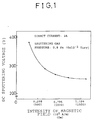
- Fig. 1 shows the relationship between the intensity of the magnetic field on the surface of the target and the discharging voltage during sputtering.
- the sputtering voltage effectively decreases with the increase in the intensity of the magnetic field.
- the decrease in the sputtering voltage is almost saturated, and the sputtering voltage becomes about 250V at 1.273 x 10 5 A/m (1600 Oe).
- the intensity of the magnetic field is further increased, the decrease in the sputtering voltage cannot be expected any more.
- this invention has an object, by eliminating the problems associated with the conventional methods, of providing a method of and an apparatus for producing a transparent conductive film with still lower electric resistance.
- the inventors of this invention Upon diligent studies to attain the above-described object, the inventors of this invention have found that the sputtering voltage can further be lowered or decreased by superimposing an RF electric field on a DC electric field for discharging purpose while, at the same time, increasing the intensity of the magnetic field on the surface of the target.
- This invention has been made on the basis of the above-described finding.
- This invention is a method of producing an In-O, Sn-O, Zn-O, Cd-Sn-O or Cd-In-O based transparent conductive film with an optional addition of a donor element, wherein the sputtering is carried out by maintaining an intensity of a magnetic field on a surface of a target at a level of 0.477 x 10 5 A/m (600 Oe) or greater and sputtering the target so as to form the transparent conductive film on a substrate by charging the target, simultaneously with said maintaining of the magnetic field intensity, with a DC electric field superimposed with an RF electric field so as to lower the sputtering voltage to 250 volts or less.
- the inventors of this invention succeeded in largely lowering the sputtering voltage below 250V by superimposing, as a means of increasing the density of plasma, the RF electric field on the DC electric field for generating the discharging.
- the superimposition of the RF electric field is effective when the intensity of the magnetic field on the surface of the target is 0.477 x 10 5 A/m (600 Oe) or more.
- the intensity of the magnetic field is below 0.477 x 10 5 A/m (600 Oe)
- the sputtering voltage contrarily increases by the superimposition of the RF electric field. Therefore, in superimposing the high-frequency electric filed, the intensity of the magnetic field on the surface of the target must be maintained at 0.477 x 10 5 A/m (600 Oe) or greater.
- an In, Sn, Zn, Cd-Sn, Cd-In based metallic target or the like or its sintered oxide based target with an addition, depending on necessity, of a donor element is used.
- Sn is generally used for an In-O based target
- Sb for an Sn-O based target
- In, Al, Si or the like for a Zn-O based target, respectively.
- the In-O based target with an addition of a small amount of Sn results in a film of the lowest resistance value. In addition, it is superior in the etching characteristics of the resultant film. It is therefore preferable to use the ITO target.
- the target may be of a sintered oxide target, and a DC power supply can be used as the electric discharging power supply because the sintered oxide target itself has a high electric conductivity.
- a mixture gas of an inert gas such, for example, as Ar or the like added by oxygen may be used.
- Ar is used as the inert gas, it is preferable to make the mixture gas pressure to the order of about 0.133 Pa (10 -3 Torr), and the oxygen partial pressure to the order of about 0.001 Pa (10 -5 Torr).
- Another aspect of this invention is an apparatus for producing an In-O, Sn-O, Zn-O, Cd-Sn-O or Cd-In-O based transparent conductive film with an optional addition of a donor element, the apparatus having a vacuum chamber adapted to support therein a substrate and a target in an opposed relationship to each other for forming by sputtering the transparent conductive film on the substrate by plasma discharge generated therebetween, wherein the apparatus comprises means for forming a magnetic field having a predetermined intensity of 0.477 x 10 5 A/m (600 Oe) or greater on a surface of the target, and power supply means for sputtering used in forming the transparent conductive film, said power supply means including DC power supply means for charging the target with a DC electric field, and RF power supply means for charging the target with a RF electric field superimposed on the DC electric field, said power supply means so constructed and arranged as to supply an electric field to the target by superimposing the RF electric field on the DC electric field while maintaining a sp
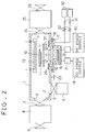
- Fig. 2 is a sectional view of an apparatus for producing a transparent conductive film according to one embodiment of this invention.
- numeral 1 denotes a vacuum chamber, i.e., a sputtering chamber.
- this sputtering chamber 1 there are provided three openings, i.e., an exhaust port 2, a loading port 3 and an unloading port 4.
- the exhaust port 2 is communicated with an evacuating means 6 such as a cryopump or the like via a valve 5 so that the sputtering chamber 1 can be adjusted in its vacuum degree by the evacuating means 6.
- an evacuating means 6 such as a cryopump or the like
- the loading port 3 is communicated with a loading chamber 8 via a valve 7.
- This loading chamber 8 is also provided at its loading port with a valve 9.
- the sputtering chamber 1 is communicated with a sputtering gas supply source 30, from which a sputter gas such, for example, as argon and oxygen is supplied independently or as a mixture gas through stop valves 31, mass flow controllers 32 and a nozzle 33.
- the partial pressures of the above-described argon gas and oxygen gas are respectively controlled for setting to the order, for example, of 0.113 Pa (10 -3 Torr) with argon gas and 0.001 Pa (10 -5 Torr) with oxygen gas.
- a substrate 11 supported on a substrate holder 10, and a sputter cathode 12.
- This substrate holder 10 is either fixed or so arranged as to be linearly movable inside the sputtering chamber 1 while maintaining a parallel relationship with the sputter cathode 12.
- a means for linearly driving the substrate holder as described above is also provided.
- a heater 13 to control the substrate temperature in the film-forming process to a predetermined temperature.
- the sputter cathode 12 is water-cooled, and on the front surface thereof there is fixed a target 14 with a brading material.
- a cathode case 17 which contains therein a permanent magnet 16 supported on a pole piece 15.
- This permanent magnet 16 is for generating a magnetic field for magnetron discharging.
- the intensity of the magnetic field on the surface of the target 14 is adjusted by varying the distance between the permanent magnet 16 and the target 14, the intensity of the magnetic field being made adjustable up to a maximum of 1.273 x 10 5 A/m (1600 Oe).
- a DC power supply means 19 as a main power supply and an RF (e.g., 13.56MHz) power supply means 20 as an auxiliary power supply are used.
- the DC power supply means 19 is connected, via an RF filter 21 for preventing the incoming RF electric field, and the RF power supply means 20 is connected via a matching box 22, respectively to the cathode case 17 and further to the sputter cathode 12.
- the sputtering chamber 1 is grounded as shown by numeral 23. It is thus so arranged that, by making the sputtering chamber 1 to be at earth potential, the cathode case 17 is charged with a negative voltage so that DC magnetron sputtering can be carried out inside the vacuum chamber 1.
- the unloading port 4 of the vacuum chamber 1 is communicated with an unloading chamber 25 via a valve 24.
- This unloading chamber 25 is also provided at its unloading port with a valve 26.
- the substrate 11 is mounted on the substrate holder 10 from the side of the loading chamber 8, and the substrate having formed a transparent conductive film on the surface thereof is unloaded from the side of the unloading chamber 25.
- numeral 27 denotes an anti-deposition plate and numeral 29 denotes an earth shield.
- a sintered target of In 2 O 3 with an addition of 10% by weight of SnO 2 was used.
- the distance between the target and the substrate was set at 80mm, and the intensity of the magnetic field was set at 1.273 x 10 5 A/m (1600 Oe), and the DC power supply was controlled to maintain a constant current supply of 2A.
- an RF electric field of 13.56MHz was superimposed, while varying the electric power, on the discharging by the DC electric field.
- the DC sputtering voltage at this time was measured.
- a sputtering gas as a sputtering gas, a mixture gas of argon and oxygen was introduced into the sputtering chamber 1, and the total pressure therein was adjusted to 0.8 Pa (6 x 10 -3 Torr).
- the results are shown in Fig. 3.
- the sputtering voltage lowered or decreased with an increase in the RF electric power when the high-frequency electric field was charged by superimposition.
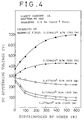
- the DC sputtering voltage was also measured when the intensity of the magnetic field was varied within the range of 0.238 x 10 5 and 1.273x10 5 A/m (300 and 1600 Oe) and, at the same time, when the RF electric field was charged by superimpostion while varying the electric power.
- the results are shown in Fig. 4. As can be seen from the graph of this figure, when the intensity of the magnetic field was 0.477x10 5 A/m (600 Oe) or greater, the DC sputtering voltage lowered by the superimposition of the RF electric field.
- the intensity of the magnetic field was 0.398 x 10 5 A/m (500 Oe) or below
- the sputtering voltage increased as a result of the superimposition of the RF electric field. Therefore, in order to lower the sputtering voltage by superimposing the RF electric field, the intensity of the magnetic field on the surface of the target must be maintained at 0.477 x 10 5 A/m (600 Oe) or greater.
- an oxide target 14 (125mm x 406mm in size) of In 2 O 3 with an addition of 10% by weight of SnO 2 and a substrate 11 made of a transparent glass (No. 7059 of Corning Co. make, 1.1mm in thickness).
- a sputtering gas a mixture gas of argon and oxygen was introduced into the sputtering chamber 1, and the total pressure therein was adjusted to 0.8 Pa (6 x 10 -3 Torr).
- the sputtering voltage was varied, in the range of 250V and more, only by varying the intensity of the magnetic field.
- the intensity of the magnetic field was 1.273 x 10 5 A/m (1600 Oe) at the sputtering voltage of 250V
- the sputtering voltage was varied in the range of 250V or less by superimposing the RF electric field while maintaining the intensity of the magnetic field at 1.273 x 10 5 A/m (1600 Oe).
- the electrical resistivity of the ITO film was measured by varying the partial pressure of oxygen in the order of 0.001 Pa (10 -5 Torr) under the respective conditions, and a most optimum value was selected.
- Film forming was carried out by moving the substrate from the side of the loading port 3 towards the side of the unloading port 4 at an equal speed, while maintaining the substrate temperature at 200°C under the above-described conditions.
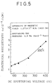
- Fig. 5 shows the relationship between the sputtering voltage and the electrical resistivity of the ITO film obtained.
- the electrical resistivities of the ITO film of as low as 1.9 x 10 -4 ⁇ cm at the sputtering voltage of 250V and 1.25 x 10 -4 ⁇ cm by still further lowering the voltage to 80V, as compared with 4.5 x 10 -4 ⁇ cm at the sputtering voltage of 420V.
- an SnO based or a ZnO based sintered body may also be used as well.
- the electric resistance is deteriorated by the incidence of the anions of oxygen or the like.
- the electrical resistivity of the formed transparent conductive film can be lowered by lowering the sputtering voltage, like in the case of using the above-described ITO based target.
Landscapes
- Chemical & Material Sciences (AREA)
- Chemical Kinetics & Catalysis (AREA)
- Engineering & Computer Science (AREA)
- Materials Engineering (AREA)
- Mechanical Engineering (AREA)
- Metallurgy (AREA)
- Organic Chemistry (AREA)
- Physical Vapour Deposition (AREA)
- Manufacturing Of Electric Cables (AREA)
- Electrodes Of Semiconductors (AREA)
- Physical Deposition Of Substances That Are Components Of Semiconductor Devices (AREA)
Claims (2)
- Verfahren zum Herstellen eines auf In-O, Sn-O, Zn-O, Cd-Sn-O oder Cd-In-O basierenden durchsichtigen leitfähigen Films mit einer wahlweisen Zugabe eines Donatorelements, umfassend die Schritte:Aufrechterhalten einer Intensität eines Magnetfeldes auf einer Oberfläche eines Targets (14) auf einen Wert von mindestens 0,477x105A/m (6000e), undSputtern des Targets (14), um auf einem Substrat (11) den durchsichtigen leitfähigen Film auszubilden, indem gleichzeitig mit dem Aufrechterhalten der Magnetfeldintensität dem Target ein elektrisches Gleichstromfeld, welches mit einem elektrischen Hochfrequenzfeld zur Verringerung der Sputterspannung auf 250 Volt oder niedriger überlagert ist, zugeführt wird.
- Vorrichtung zum Herstellen eines auf In-O, Sn-O, Cd-Sn-O oder Cd-In-O basierenden durchsichtigen leitfähigen Films mit einer wahlweisen Zugabe eines Donatorelementes, umfassend:eine Vakuumkammer (1), die zur Aufnahme eines Substrats (11) und eines Targets (14) in gegenüberliegender Anordnung darin geeignet ist, um auf dem Substrat (11) durch Sputtern den durchsichtigen leitfähigen Film durch eine Plasmaentladung zwischen dem Target (14) und dem Substrat (11) auszubilden,Mittel (16) zum Erzeugen eines Magnetfeldes mit einer bestimmten Intensität von mindestens 0,477x105A/m (6000e) auf der Oberfläche des Targets (14), undStromversorgungsmittel zum Sputtern, die zum Ausbilden des durchsichtigen leitfähigen Films verwendet werden, wobei die Stromversorgungsmittel Gleichstromversorgungsmittel (19) umfassen, um dem Target (14) ein elektrisches Gleichstromfeld zuzuführen, sowie Hochfrequenz-Stromversorgungsmittel (20) zum Überlagern des elektrischen Gleichstromfeldes mit einem elektrischen Hochfrequenzfeld., wobei die Stromversorgungsmittel (19, 20) derart ausgebildet und angeordnet sind, daß das Target einem elektrischen Feld ausgesetzt wird, indem das elektrische Gleichstromfeld mit dem elektrischen Hochfrequenzfeld überlagert wird, während eine Sputterspannung bei der Ausbildung des durchsichtigen leitfähigen Films auf höchstens 250 Volt gehalten wird.
Applications Claiming Priority (2)
| Application Number | Priority Date | Filing Date | Title |
|---|---|---|---|
| JP44558/90 | 1990-02-27 | ||
| JP2044558A JP2936276B2 (ja) | 1990-02-27 | 1990-02-27 | 透明導電膜の製造方法およびその製造装置 |
Publications (3)
| Publication Number | Publication Date |
|---|---|
| EP0447850A2 EP0447850A2 (de) | 1991-09-25 |
| EP0447850A3 EP0447850A3 (en) | 1993-10-27 |
| EP0447850B1 true EP0447850B1 (de) | 1996-12-18 |
Family
ID=12694830
Family Applications (1)
| Application Number | Title | Priority Date | Filing Date |
|---|---|---|---|
| EP91102978A Expired - Lifetime EP0447850B1 (de) | 1990-02-27 | 1991-02-27 | Verfahren und Vorrichtung zum Herstellen eines durchsichtigen leitenden Films |
Country Status (5)
| Country | Link |
|---|---|
| US (1) | US5180476A (de) |
| EP (1) | EP0447850B1 (de) |
| JP (1) | JP2936276B2 (de) |
| KR (1) | KR950000009B1 (de) |
| DE (1) | DE69123618T2 (de) |
Cited By (1)
| Publication number | Priority date | Publication date | Assignee | Title |
|---|---|---|---|---|
| RU2206634C2 (ru) * | 2001-07-10 | 2003-06-20 | Брагин Вадим Игоревич | Отражающее покрытие |
Families Citing this family (51)
| Publication number | Priority date | Publication date | Assignee | Title |
|---|---|---|---|---|
| JPH07509534A (ja) * | 1991-12-28 | 1995-10-19 | ハイヤー ヴァキュウム インダストリ カンパニー リミテッド | 発熱反射ガラスと発熱透明ガラス及びそれらの製造方法 |
| JP2905342B2 (ja) * | 1992-09-07 | 1999-06-14 | 財団法人国際超電導産業技術研究センター | YBa2Cu3Ox超電導薄膜の製造方法 |
| JP2912506B2 (ja) * | 1992-10-21 | 1999-06-28 | シャープ株式会社 | 透明導電膜の形成方法 |
| FR2699934B1 (fr) * | 1992-12-30 | 1995-03-17 | Lorraine Inst Nat Polytech | Procédé de contrôle de la concentration en métalloïde d'un dépôt réalisés par voie physique en phase vapeur réactive à l'aide d'un plasma froid de pulvérisation. |
| JPH0715051A (ja) * | 1993-06-24 | 1995-01-17 | Mitsubishi Electric Corp | Ybco超電導薄膜の製造方法 |
| EP0639655B1 (de) * | 1993-07-28 | 2000-09-27 | Asahi Glass Company Ltd. | Verfahren und Vorrichtung zur Kathodenzerstäubung |
| DE69431573T2 (de) * | 1993-07-28 | 2003-06-12 | Asahi Glass Co., Ltd. | Verfahren zur Herstellung von Schichten |
| JP2642849B2 (ja) * | 1993-08-24 | 1997-08-20 | 株式会社フロンテック | 薄膜の製造方法および製造装置 |
| FR2711450B1 (fr) * | 1993-10-18 | 1996-01-05 | Pixel Int Sa | Installation et procédé pour la fabrication d'écrans plats de visualisation. |
| DE4336830A1 (de) * | 1993-10-28 | 1995-05-04 | Leybold Ag | Plasma-Zerstäubungsanlage mit Mikrowellenunterstützung |
| US5708233A (en) * | 1994-02-22 | 1998-01-13 | Kabushiki Kaisha Ohara | Thermoelectric semiconductor material |
| JPH07278795A (ja) * | 1994-04-13 | 1995-10-24 | Showa Techno Kooto Kk | 紫外線及び赤外線の遮蔽機能を有する透明な合成樹脂製スクリーン用材料の製造方法 |
| DE4413378A1 (de) * | 1994-04-19 | 1995-10-26 | Leybold Ag | Einrichtung zum Beschichten eines Substrats |
| JPH07316810A (ja) * | 1994-05-27 | 1995-12-05 | Fuji Xerox Co Ltd | スパッタリング装置 |
| JP3119172B2 (ja) | 1995-09-13 | 2000-12-18 | 日新電機株式会社 | プラズマcvd法及び装置 |
| US6137048A (en) * | 1996-11-07 | 2000-10-24 | Midwest Research Institute | Process for fabricating polycrystalline semiconductor thin-film solar cells, and cells produced thereby |
| JPH11302843A (ja) * | 1998-02-17 | 1999-11-02 | Canon Inc | 酸化亜鉛膜の堆積方法および堆積装置、光起電力素子 |
| GB2342927B (en) * | 1998-10-23 | 2003-05-07 | Trikon Holdings Ltd | Apparatus and methods for sputtering |
| JP4510967B2 (ja) * | 1999-12-03 | 2010-07-28 | 大阪府 | 導電性光選択透過シート |
| GB2361244B (en) * | 2000-04-14 | 2004-02-11 | Trikon Holdings Ltd | A method of depositing dielectric |
| DE10023459A1 (de) * | 2000-05-12 | 2001-11-15 | Balzers Process Systems Gmbh | Indium-Zinn-Oxid (ITO)-Schicht und Verfahren zur Herstellung derselben |
| CN1237199C (zh) * | 2000-06-21 | 2006-01-18 | 日本板硝子株式会社 | 具有透明导电薄膜的基片和使用该基片的有机电致发光装置 |
| US20030159925A1 (en) * | 2001-01-29 | 2003-08-28 | Hiroaki Sako | Spattering device |
| JP2003239069A (ja) * | 2002-02-15 | 2003-08-27 | Ulvac Japan Ltd | 薄膜の製造方法及び装置 |
| DE10224990B3 (de) * | 2002-06-05 | 2004-03-11 | Fraunhofer-Gesellschaft zur Förderung der angewandten Forschung e.V. | Verfahren zur Abscheidung transparenter leitfähiger Schichten |
| JP2006162686A (ja) * | 2004-12-02 | 2006-06-22 | Ricoh Co Ltd | 光偏向素子、該素子を備えた光偏向装置及び画像表示装置 |
| TWI310408B (en) * | 2004-12-23 | 2009-06-01 | Ind Tech Res Inst | Cadmium tin oxide multi-layer laminate and its producing method |
| US20070040501A1 (en) * | 2005-08-18 | 2007-02-22 | Aitken Bruce G | Method for inhibiting oxygen and moisture degradation of a device and the resulting device |
| US7722929B2 (en) * | 2005-08-18 | 2010-05-25 | Corning Incorporated | Sealing technique for decreasing the time it takes to hermetically seal a device and the resulting hermetically sealed device |
| US7829147B2 (en) * | 2005-08-18 | 2010-11-09 | Corning Incorporated | Hermetically sealing a device without a heat treating step and the resulting hermetically sealed device |
| EP2194157A4 (de) * | 2007-08-24 | 2012-08-01 | Ulvac Inc | Verfahren zur formung einer transparenten leitfähigen folie |
| CL2008002636A1 (es) | 2007-09-07 | 2009-06-19 | Avery Dennison Corp | Un rótulo para cubrir identificación existente en sustratos como paquetes o envases de tal manera que el sustrato puede ser reutilizado, hoja de rótulos y método de fabricación. |
| EP2197043A4 (de) * | 2007-09-19 | 2012-06-27 | Ulvac Inc | Solarbatterie-herstellungsverfahren |
| CN101790795A (zh) * | 2007-09-19 | 2010-07-28 | 株式会社爱发科 | 太阳能电池的制造方法 |
| JPWO2009084441A1 (ja) * | 2007-12-28 | 2011-05-19 | 株式会社アルバック | 透明導電膜の成膜方法及び成膜装置 |
| DE112009000156T5 (de) * | 2008-01-24 | 2011-06-22 | ULVAC, Inc., Kanagawa | Verfahren zur Herstellung einer Flüssigkristallanzeigevorrichtung |
| CN102439697B (zh) * | 2009-04-03 | 2015-08-19 | 应用材料公司 | 高压rf-dc溅射及改善此工艺的膜均匀性和阶梯覆盖率的方法 |
| US20120160663A1 (en) * | 2010-12-14 | 2012-06-28 | Alliance For Sustainable Energy, Llc. | Sputter Deposition and Annealing of High Conductivity Transparent Oxides |
| KR20140074922A (ko) * | 2011-09-07 | 2014-06-18 | 어플라이드 머티어리얼스, 인코포레이티드 | 터치 패널에서 사용하기 위한 투명 보디를 제조하는 방법 및 시스템 |
| JP6228846B2 (ja) * | 2011-11-28 | 2017-11-08 | 日東電工株式会社 | 透明導電性フィルムの製造方法 |
| JP6215062B2 (ja) * | 2013-01-16 | 2017-10-18 | 日東電工株式会社 | 透明導電フィルムの製造方法 |
| JP6261987B2 (ja) * | 2013-01-16 | 2018-01-17 | 日東電工株式会社 | 透明導電フィルムおよびその製造方法 |
| JP5976846B2 (ja) * | 2013-01-16 | 2016-08-24 | 日東電工株式会社 | 透明導電フィルムおよびその製造方法 |
| JP6261988B2 (ja) * | 2013-01-16 | 2018-01-17 | 日東電工株式会社 | 透明導電フィルムおよびその製造方法 |
| JP2014220272A (ja) * | 2013-05-01 | 2014-11-20 | 株式会社アルバック | 発光ダイオードの製造方法 |
| DE102013210155A1 (de) | 2013-05-31 | 2014-12-04 | Fraunhofer-Gesellschaft zur Förderung der angewandten Forschung e.V. | Verfahren zum Abscheiden einer transparenten, elektrisch leitfähigen Metalloxidschicht |
| JP5613805B2 (ja) * | 2013-09-02 | 2014-10-29 | 学校法人金沢工業大学 | 酸化亜鉛系透明導電膜、マグネトロンスパッタリング用焼結体ターゲット、液晶ディスプレイ及びタッチパネル、ならびに酸化亜鉛系透明導電膜を含んでなる機器 |
| JP6211557B2 (ja) | 2014-04-30 | 2017-10-11 | 日東電工株式会社 | 透明導電性フィルム及びその製造方法 |
| CN106460153B (zh) * | 2014-04-30 | 2019-05-10 | 日东电工株式会社 | 透明导电性膜及其制造方法 |
| CN105637111A (zh) * | 2014-05-20 | 2016-06-01 | 日东电工株式会社 | 透明导电性薄膜及其制造方法 |
| WO2016144312A1 (en) | 2015-03-09 | 2016-09-15 | Whirlpool Corporation | Microwave oven having door with transparent panel |
Citations (1)
| Publication number | Priority date | Publication date | Assignee | Title |
|---|---|---|---|---|
| EP0416241A2 (de) * | 1989-09-07 | 1991-03-13 | Leybold Aktiengesellschaft | Vorrichtung zum Beschichten eines Substrats |
Family Cites Families (7)
| Publication number | Priority date | Publication date | Assignee | Title |
|---|---|---|---|---|
| DE3300525A1 (de) * | 1983-01-10 | 1984-07-12 | Merck Patent Gmbh, 6100 Darmstadt | Targets fuer die kathodenzerstaeubung |
| US4500408A (en) * | 1983-07-19 | 1985-02-19 | Varian Associates, Inc. | Apparatus for and method of controlling sputter coating |
| JPS60132319A (ja) * | 1983-12-20 | 1985-07-15 | Fuji Xerox Co Ltd | 薄膜形成方法 |
| JPS63109164A (ja) * | 1986-10-27 | 1988-05-13 | Seiko Epson Corp | マグネトロンスパツタ装置 |
| US4849081A (en) * | 1988-06-22 | 1989-07-18 | The Boc Group, Inc. | Formation of oxide films by reactive sputtering |
| JPH0772346B2 (ja) * | 1989-03-03 | 1995-08-02 | 日本真空技術株式会社 | 低抵抗透明導電膜の製造方法 |
| EP0421015B1 (de) * | 1989-10-06 | 1995-01-18 | Nihon Shinku Gijutsu Kabushiki Kaisha | Verfahren zur Herstellung eines leitenden, durchsichtigen Films |
-
1990
- 1990-02-27 JP JP2044558A patent/JP2936276B2/ja not_active Expired - Lifetime
-
1991
- 1991-02-26 KR KR1019910003106A patent/KR950000009B1/ko not_active Expired - Lifetime
- 1991-02-26 US US07/660,840 patent/US5180476A/en not_active Expired - Lifetime
- 1991-02-27 EP EP91102978A patent/EP0447850B1/de not_active Expired - Lifetime
- 1991-02-27 DE DE69123618T patent/DE69123618T2/de not_active Expired - Lifetime
Patent Citations (1)
| Publication number | Priority date | Publication date | Assignee | Title |
|---|---|---|---|---|
| EP0416241A2 (de) * | 1989-09-07 | 1991-03-13 | Leybold Aktiengesellschaft | Vorrichtung zum Beschichten eines Substrats |
Cited By (1)
| Publication number | Priority date | Publication date | Assignee | Title |
|---|---|---|---|---|
| RU2206634C2 (ru) * | 2001-07-10 | 2003-06-20 | Брагин Вадим Игоревич | Отражающее покрытие |
Also Published As
| Publication number | Publication date |
|---|---|
| JP2936276B2 (ja) | 1999-08-23 |
| US5180476A (en) | 1993-01-19 |
| EP0447850A2 (de) | 1991-09-25 |
| KR910021495A (ko) | 1991-12-20 |
| EP0447850A3 (en) | 1993-10-27 |
| KR950000009B1 (ko) | 1995-01-07 |
| DE69123618D1 (de) | 1997-01-30 |
| DE69123618T2 (de) | 1997-07-03 |
| JPH03249171A (ja) | 1991-11-07 |
Similar Documents
| Publication | Publication Date | Title |
|---|---|---|
| EP0447850B1 (de) | Verfahren und Vorrichtung zum Herstellen eines durchsichtigen leitenden Films | |
| US4046660A (en) | Sputter coating with charged particle flux control | |
| US7879209B2 (en) | Cathode for sputter coating | |
| US5116479A (en) | Process for producing transparent conductive film comprising indium oxide | |
| WO2004106581A2 (en) | Transparent conductive oxides | |
| EP0385475A2 (de) | Verfahren zur Herstellung eines durchsichtigen leitenden Films | |
| US20090127098A1 (en) | Sputtering apparatus of forming thin film | |
| Webb | Conductivity imaging of the erosion pattern for ZnO prepared by planar RF magnetron sputtering | |
| EP0421015B1 (de) | Verfahren zur Herstellung eines leitenden, durchsichtigen Films | |
| US20050211550A1 (en) | Device for reactive sputtering | |
| US6495000B1 (en) | System and method for DC sputtering oxide films with a finned anode | |
| Ridge et al. | The application of ion plating to the continuous coating of flexible plastic sheet | |
| US3516915A (en) | Sputtering technique | |
| JPH09316632A (ja) | 透明材料からなる支持体の上に光学的に透明でかつ導電性の層を付着させるための方法 | |
| US20060049041A1 (en) | Anode for sputter coating | |
| JPH09170077A (ja) | 真空処理チャンバ、真空チャンバ用マグネトロン装置および真空スパッタリング法 | |
| Petrov et al. | Effect of ion bombardment during growth on the electrical resistivity of magnetron-sputtered carbon films | |
| JPH0892740A (ja) | マグネトロンスパッタ装置 | |
| JP2633340B2 (ja) | 透明導電膜の形成方法 | |
| JPH0273963A (ja) | 低温基体への薄膜形成方法 | |
| JP3968128B2 (ja) | 薄膜抵抗体の成膜方法及び装置 | |
| JPH06330283A (ja) | 透明導電膜の成膜装置および成膜方法 | |
| Uetani et al. | Ultra thin TiN films prepared by an advanced ion-plating method | |
| JP3528930B2 (ja) | 透明導電膜の製造方法 | |
| JPH062123A (ja) | スパッタリング成膜装置 |
Legal Events
| Date | Code | Title | Description |
|---|---|---|---|
| PUAI | Public reference made under article 153(3) epc to a published international application that has entered the european phase |
Free format text: ORIGINAL CODE: 0009012 |
|
| AK | Designated contracting states |
Kind code of ref document: A2 Designated state(s): DE FR NL |
|
| PUAL | Search report despatched |
Free format text: ORIGINAL CODE: 0009013 |
|
| AK | Designated contracting states |
Kind code of ref document: A3 Designated state(s): DE FR NL |
|
| 17P | Request for examination filed |
Effective date: 19940407 |
|
| 17Q | First examination report despatched |
Effective date: 19941207 |
|
| GRAG | Despatch of communication of intention to grant |
Free format text: ORIGINAL CODE: EPIDOS AGRA |
|
| GRAH | Despatch of communication of intention to grant a patent |
Free format text: ORIGINAL CODE: EPIDOS IGRA |
|
| GRAH | Despatch of communication of intention to grant a patent |
Free format text: ORIGINAL CODE: EPIDOS IGRA |
|
| GRAA | (expected) grant |
Free format text: ORIGINAL CODE: 0009210 |
|
| AK | Designated contracting states |
Kind code of ref document: B1 Designated state(s): DE FR NL |
|
| REF | Corresponds to: |
Ref document number: 69123618 Country of ref document: DE Date of ref document: 19970130 |
|
| ET | Fr: translation filed | ||
| ET | Fr: translation filed |
Free format text: CORRECTIONS |
|
| PLBE | No opposition filed within time limit |
Free format text: ORIGINAL CODE: 0009261 |
|
| STAA | Information on the status of an ep patent application or granted ep patent |
Free format text: STATUS: NO OPPOSITION FILED WITHIN TIME LIMIT |
|
| 26N | No opposition filed | ||
| PGFP | Annual fee paid to national office [announced via postgrant information from national office to epo] |
Ref country code: FR Payment date: 20100226 Year of fee payment: 20 |
|
| PGFP | Annual fee paid to national office [announced via postgrant information from national office to epo] |
Ref country code: NL Payment date: 20100215 Year of fee payment: 20 Ref country code: DE Payment date: 20100429 Year of fee payment: 20 |
|
| REG | Reference to a national code |
Ref country code: DE Ref legal event code: R071 Ref document number: 69123618 Country of ref document: DE |
|
| REG | Reference to a national code |
Ref country code: NL Ref legal event code: V4 Effective date: 20110227 |
|
| PG25 | Lapsed in a contracting state [announced via postgrant information from national office to epo] |
Ref country code: NL Free format text: LAPSE BECAUSE OF EXPIRATION OF PROTECTION Effective date: 20110227 |
|
| PG25 | Lapsed in a contracting state [announced via postgrant information from national office to epo] |
Ref country code: DE Free format text: LAPSE BECAUSE OF EXPIRATION OF PROTECTION Effective date: 20110227 |