US6137048A - Process for fabricating polycrystalline semiconductor thin-film solar cells, and cells produced thereby - Google Patents
Process for fabricating polycrystalline semiconductor thin-film solar cells, and cells produced thereby Download PDFInfo
- Publication number
- US6137048A US6137048A US09/218,206 US21820698A US6137048A US 6137048 A US6137048 A US 6137048A US 21820698 A US21820698 A US 21820698A US 6137048 A US6137048 A US 6137048A
- Authority
- US
- United States
- Prior art keywords
- layer
- cadmium
- stannate
- temperature
- depositing
- Prior art date
- Legal status (The legal status is an assumption and is not a legal conclusion. Google has not performed a legal analysis and makes no representation as to the accuracy of the status listed.)
- Expired - Lifetime
Links
- 238000000034 method Methods 0.000 title claims abstract description 90
- 239000004065 semiconductor Substances 0.000 title claims abstract description 62
- 239000010409 thin film Substances 0.000 title claims abstract description 32
- 230000008569 process Effects 0.000 title description 36
- 229910052980 cadmium sulfide Inorganic materials 0.000 claims abstract description 109
- WUPHOULIZUERAE-UHFFFAOYSA-N 3-(oxolan-2-yl)propanoic acid Chemical compound OC(=O)CCC1CCCO1 WUPHOULIZUERAE-UHFFFAOYSA-N 0.000 claims abstract description 106
- MARUHZGHZWCEQU-UHFFFAOYSA-N 5-phenyl-2h-tetrazole Chemical compound C1=CC=CC=C1C1=NNN=N1 MARUHZGHZWCEQU-UHFFFAOYSA-N 0.000 claims abstract description 88
- 229910052793 cadmium Inorganic materials 0.000 claims abstract description 74
- 229940071182 stannate Drugs 0.000 claims abstract description 70
- 238000000151 deposition Methods 0.000 claims abstract description 52
- BNEMLSQAJOPTGK-UHFFFAOYSA-N zinc;dioxido(oxo)tin Chemical compound [Zn+2].[O-][Sn]([O-])=O BNEMLSQAJOPTGK-UHFFFAOYSA-N 0.000 claims abstract description 43
- 239000000758 substrate Substances 0.000 claims abstract description 37
- 239000000463 material Substances 0.000 claims abstract description 35
- 238000004544 sputter deposition Methods 0.000 claims abstract description 23
- 238000010438 heat treatment Methods 0.000 claims abstract description 17
- 238000002202 sandwich sublimation Methods 0.000 claims abstract description 17
- 239000011029 spinel Substances 0.000 claims abstract description 11
- 229910052596 spinel Inorganic materials 0.000 claims abstract description 11
- 239000013078 crystal Substances 0.000 claims abstract description 10
- 239000010408 film Substances 0.000 claims description 89
- YKYOUMDCQGMQQO-UHFFFAOYSA-L cadmium dichloride Chemical compound Cl[Cd]Cl YKYOUMDCQGMQQO-UHFFFAOYSA-L 0.000 claims description 32
- 238000004519 manufacturing process Methods 0.000 claims description 13
- 238000005240 physical vapour deposition Methods 0.000 claims description 7
- 238000004070 electrodeposition Methods 0.000 claims description 6
- 238000007650 screen-printing Methods 0.000 claims description 5
- 238000005507 spraying Methods 0.000 claims description 4
- 229910004613 CdTe Inorganic materials 0.000 claims description 3
- UFHFLCQGNIYNRP-UHFFFAOYSA-N Hydrogen Chemical compound [H][H] UFHFLCQGNIYNRP-UHFFFAOYSA-N 0.000 claims description 3
- 239000001257 hydrogen Substances 0.000 claims description 3
- 229910052739 hydrogen Inorganic materials 0.000 claims description 3
- XOLBLPGZBRYERU-UHFFFAOYSA-N tin dioxide Chemical compound O=[Sn]=O XOLBLPGZBRYERU-UHFFFAOYSA-N 0.000 description 37
- 229910001887 tin oxide Inorganic materials 0.000 description 17
- 230000003287 optical effect Effects 0.000 description 16
- 230000008021 deposition Effects 0.000 description 15
- 230000008901 benefit Effects 0.000 description 13
- 230000005540 biological transmission Effects 0.000 description 12
- 238000001552 radio frequency sputter deposition Methods 0.000 description 12
- 238000010521 absorption reaction Methods 0.000 description 11
- 238000006243 chemical reaction Methods 0.000 description 11
- 238000000137 annealing Methods 0.000 description 10
- 238000012545 processing Methods 0.000 description 8
- 230000003746 surface roughness Effects 0.000 description 8
- 230000002829 reductive effect Effects 0.000 description 7
- BDOSMKKIYDKNTQ-UHFFFAOYSA-N cadmium atom Chemical compound [Cd] BDOSMKKIYDKNTQ-UHFFFAOYSA-N 0.000 description 6
- 238000003486 chemical etching Methods 0.000 description 6
- 241000223080 Sweet potato virus C Species 0.000 description 5
- 230000015572 biosynthetic process Effects 0.000 description 5
- 238000005229 chemical vapour deposition Methods 0.000 description 5
- 230000007423 decrease Effects 0.000 description 5
- PXHVJJICTQNCMI-UHFFFAOYSA-N Nickel Chemical compound [Ni] PXHVJJICTQNCMI-UHFFFAOYSA-N 0.000 description 4
- XLOMVQKBTHCTTD-UHFFFAOYSA-N Zinc monoxide Chemical compound [Zn]=O XLOMVQKBTHCTTD-UHFFFAOYSA-N 0.000 description 4
- 238000000224 chemical solution deposition Methods 0.000 description 4
- 229910052738 indium Inorganic materials 0.000 description 4
- APFVFJFRJDLVQX-UHFFFAOYSA-N indium atom Chemical compound [In] APFVFJFRJDLVQX-UHFFFAOYSA-N 0.000 description 4
- 229910052751 metal Inorganic materials 0.000 description 4
- 239000002184 metal Substances 0.000 description 4
- 230000005855 radiation Effects 0.000 description 4
- 239000011701 zinc Substances 0.000 description 4
- OKTJSMMVPCPJKN-UHFFFAOYSA-N Carbon Chemical compound [C] OKTJSMMVPCPJKN-UHFFFAOYSA-N 0.000 description 3
- VYPSYNLAJGMNEJ-UHFFFAOYSA-N Silicium dioxide Chemical compound O=[Si]=O VYPSYNLAJGMNEJ-UHFFFAOYSA-N 0.000 description 3
- 230000002411 adverse Effects 0.000 description 3
- 239000012298 atmosphere Substances 0.000 description 3
- QVGXLLKOCUKJST-UHFFFAOYSA-N atomic oxygen Chemical compound [O] QVGXLLKOCUKJST-UHFFFAOYSA-N 0.000 description 3
- 239000010949 copper Substances 0.000 description 3
- 230000001627 detrimental effect Effects 0.000 description 3
- 230000005670 electromagnetic radiation Effects 0.000 description 3
- 239000011521 glass Substances 0.000 description 3
- 229910002804 graphite Inorganic materials 0.000 description 3
- 239000010439 graphite Substances 0.000 description 3
- 230000006872 improvement Effects 0.000 description 3
- 238000012986 modification Methods 0.000 description 3
- 230000004048 modification Effects 0.000 description 3
- 229910052760 oxygen Inorganic materials 0.000 description 3
- 239000001301 oxygen Substances 0.000 description 3
- 230000009467 reduction Effects 0.000 description 3
- 230000004044 response Effects 0.000 description 3
- 230000003595 spectral effect Effects 0.000 description 3
- 239000000126 substance Substances 0.000 description 3
- 229910052725 zinc Inorganic materials 0.000 description 3
- XKRFYHLGVUSROY-UHFFFAOYSA-N Argon Chemical compound [Ar] XKRFYHLGVUSROY-UHFFFAOYSA-N 0.000 description 2
- RYGMFSIKBFXOCR-UHFFFAOYSA-N Copper Chemical compound [Cu] RYGMFSIKBFXOCR-UHFFFAOYSA-N 0.000 description 2
- GRYLNZFGIOXLOG-UHFFFAOYSA-N Nitric acid Chemical compound O[N+]([O-])=O GRYLNZFGIOXLOG-UHFFFAOYSA-N 0.000 description 2
- NBIIXXVUZAFLBC-UHFFFAOYSA-N Phosphoric acid Chemical compound OP(O)(O)=O NBIIXXVUZAFLBC-UHFFFAOYSA-N 0.000 description 2
- BUGBHKTXTAQXES-UHFFFAOYSA-N Selenium Chemical compound [Se] BUGBHKTXTAQXES-UHFFFAOYSA-N 0.000 description 2
- HCHKCACWOHOZIP-UHFFFAOYSA-N Zinc Chemical compound [Zn] HCHKCACWOHOZIP-UHFFFAOYSA-N 0.000 description 2
- 229910007709 ZnTe Inorganic materials 0.000 description 2
- 239000006117 anti-reflective coating Substances 0.000 description 2
- 230000015556 catabolic process Effects 0.000 description 2
- 239000011248 coating agent Substances 0.000 description 2
- 238000000576 coating method Methods 0.000 description 2
- 238000007796 conventional method Methods 0.000 description 2
- 238000001816 cooling Methods 0.000 description 2
- 229910052802 copper Inorganic materials 0.000 description 2
- 230000007547 defect Effects 0.000 description 2
- 238000006731 degradation reaction Methods 0.000 description 2
- 230000000694 effects Effects 0.000 description 2
- 238000005530 etching Methods 0.000 description 2
- 238000001704 evaporation Methods 0.000 description 2
- PCHJSUWPFVWCPO-UHFFFAOYSA-N gold Chemical compound [Au] PCHJSUWPFVWCPO-UHFFFAOYSA-N 0.000 description 2
- 229910052737 gold Inorganic materials 0.000 description 2
- 239000010931 gold Substances 0.000 description 2
- 229910003437 indium oxide Inorganic materials 0.000 description 2
- PJXISJQVUVHSOJ-UHFFFAOYSA-N indium(iii) oxide Chemical compound [O-2].[O-2].[O-2].[In+3].[In+3] PJXISJQVUVHSOJ-UHFFFAOYSA-N 0.000 description 2
- AMGQUBHHOARCQH-UHFFFAOYSA-N indium;oxotin Chemical compound [In].[Sn]=O AMGQUBHHOARCQH-UHFFFAOYSA-N 0.000 description 2
- 239000006193 liquid solution Substances 0.000 description 2
- 238000001755 magnetron sputter deposition Methods 0.000 description 2
- 238000005259 measurement Methods 0.000 description 2
- 229910052759 nickel Inorganic materials 0.000 description 2
- 229910017604 nitric acid Inorganic materials 0.000 description 2
- 229910052711 selenium Inorganic materials 0.000 description 2
- 239000011669 selenium Substances 0.000 description 2
- 238000009718 spray deposition Methods 0.000 description 2
- 229910052718 tin Inorganic materials 0.000 description 2
- 239000011787 zinc oxide Substances 0.000 description 2
- 229910004611 CdZnTe Inorganic materials 0.000 description 1
- GYHNNYVSQQEPJS-UHFFFAOYSA-N Gallium Chemical compound [Ga] GYHNNYVSQQEPJS-UHFFFAOYSA-N 0.000 description 1
- 230000005355 Hall effect Effects 0.000 description 1
- 229910004262 HgTe Inorganic materials 0.000 description 1
- VEXZGXHMUGYJMC-UHFFFAOYSA-N Hydrochloric acid Chemical compound Cl VEXZGXHMUGYJMC-UHFFFAOYSA-N 0.000 description 1
- 238000004566 IR spectroscopy Methods 0.000 description 1
- NINIDFKCEFEMDL-UHFFFAOYSA-N Sulfur Chemical compound [S] NINIDFKCEFEMDL-UHFFFAOYSA-N 0.000 description 1
- UCKMPCXJQFINFW-UHFFFAOYSA-N Sulphide Chemical compound [S-2] UCKMPCXJQFINFW-UHFFFAOYSA-N 0.000 description 1
- ATJFFYVFTNAWJD-UHFFFAOYSA-N Tin Chemical compound [Sn] ATJFFYVFTNAWJD-UHFFFAOYSA-N 0.000 description 1
- 238000002441 X-ray diffraction Methods 0.000 description 1
- 239000002253 acid Substances 0.000 description 1
- 150000007513 acids Chemical class 0.000 description 1
- 238000005275 alloying Methods 0.000 description 1
- 229910000147 aluminium phosphate Inorganic materials 0.000 description 1
- 229910021417 amorphous silicon Inorganic materials 0.000 description 1
- 229910052786 argon Inorganic materials 0.000 description 1
- 239000012300 argon atmosphere Substances 0.000 description 1
- 238000000089 atomic force micrograph Methods 0.000 description 1
- 238000004630 atomic force microscopy Methods 0.000 description 1
- 230000004888 barrier function Effects 0.000 description 1
- 230000009286 beneficial effect Effects 0.000 description 1
- 230000003139 buffering effect Effects 0.000 description 1
- 230000000052 comparative effect Effects 0.000 description 1
- 150000001875 compounds Chemical class 0.000 description 1
- 239000004020 conductor Substances 0.000 description 1
- 238000010276 construction Methods 0.000 description 1
- 238000005336 cracking Methods 0.000 description 1
- 238000002425 crystallisation Methods 0.000 description 1
- 230000008025 crystallization Effects 0.000 description 1
- 230000003247 decreasing effect Effects 0.000 description 1
- 230000003111 delayed effect Effects 0.000 description 1
- 238000009792 diffusion process Methods 0.000 description 1
- 239000002019 doping agent Substances 0.000 description 1
- 238000005516 engineering process Methods 0.000 description 1
- 230000008020 evaporation Effects 0.000 description 1
- 229910052733 gallium Inorganic materials 0.000 description 1
- -1 gold or nickel Chemical class 0.000 description 1
- 229910000041 hydrogen chloride Inorganic materials 0.000 description 1
- 238000007689 inspection Methods 0.000 description 1
- 230000000670 limiting effect Effects 0.000 description 1
- 239000010808 liquid waste Substances 0.000 description 1
- 229910001635 magnesium fluoride Inorganic materials 0.000 description 1
- 229910052976 metal sulfide Inorganic materials 0.000 description 1
- 150000002739 metals Chemical class 0.000 description 1
- 239000000203 mixture Substances 0.000 description 1
- 150000002902 organometallic compounds Chemical class 0.000 description 1
- 230000036961 partial effect Effects 0.000 description 1
- 238000002161 passivation Methods 0.000 description 1
- 230000001681 protective effect Effects 0.000 description 1
- 239000010453 quartz Substances 0.000 description 1
- 238000005546 reactive sputtering Methods 0.000 description 1
- 238000001953 recrystallisation Methods 0.000 description 1
- 238000007670 refining Methods 0.000 description 1
- 238000011160 research Methods 0.000 description 1
- 235000019592 roughness Nutrition 0.000 description 1
- 238000004626 scanning electron microscopy Methods 0.000 description 1
- 230000003678 scratch resistant effect Effects 0.000 description 1
- 229910052710 silicon Inorganic materials 0.000 description 1
- 239000010703 silicon Substances 0.000 description 1
- 239000000377 silicon dioxide Substances 0.000 description 1
- 239000005361 soda-lime glass Substances 0.000 description 1
- 239000007921 spray Substances 0.000 description 1
- 229910052717 sulfur Inorganic materials 0.000 description 1
- 239000011593 sulfur Substances 0.000 description 1
- 230000001502 supplementing effect Effects 0.000 description 1
- 229910052714 tellurium Inorganic materials 0.000 description 1
- PORWMNRCUJJQNO-UHFFFAOYSA-N tellurium atom Chemical compound [Te] PORWMNRCUJJQNO-UHFFFAOYSA-N 0.000 description 1
- 238000012360 testing method Methods 0.000 description 1
- 238000005979 thermal decomposition reaction Methods 0.000 description 1
- 238000002834 transmittance Methods 0.000 description 1
- 239000012780 transparent material Substances 0.000 description 1
Images


Classifications
-
- H—ELECTRICITY
- H10—SEMICONDUCTOR DEVICES; ELECTRIC SOLID-STATE DEVICES NOT OTHERWISE PROVIDED FOR
- H10F—INORGANIC SEMICONDUCTOR DEVICES SENSITIVE TO INFRARED RADIATION, LIGHT, ELECTROMAGNETIC RADIATION OF SHORTER WAVELENGTH OR CORPUSCULAR RADIATION
- H10F10/00—Individual photovoltaic cells, e.g. solar cells
- H10F10/10—Individual photovoltaic cells, e.g. solar cells having potential barriers
- H10F10/16—Photovoltaic cells having only PN heterojunction potential barriers
- H10F10/162—Photovoltaic cells having only PN heterojunction potential barriers comprising only Group II-VI materials, e.g. CdS/CdTe photovoltaic cells
-
- H—ELECTRICITY
- H10—SEMICONDUCTOR DEVICES; ELECTRIC SOLID-STATE DEVICES NOT OTHERWISE PROVIDED FOR
- H10F—INORGANIC SEMICONDUCTOR DEVICES SENSITIVE TO INFRARED RADIATION, LIGHT, ELECTROMAGNETIC RADIATION OF SHORTER WAVELENGTH OR CORPUSCULAR RADIATION
- H10F71/00—Manufacture or treatment of devices covered by this subclass
- H10F71/125—The active layers comprising only Group II-VI materials, e.g. CdS, ZnS or CdTe
-
- H—ELECTRICITY
- H10—SEMICONDUCTOR DEVICES; ELECTRIC SOLID-STATE DEVICES NOT OTHERWISE PROVIDED FOR
- H10F—INORGANIC SEMICONDUCTOR DEVICES SENSITIVE TO INFRARED RADIATION, LIGHT, ELECTROMAGNETIC RADIATION OF SHORTER WAVELENGTH OR CORPUSCULAR RADIATION
- H10F71/00—Manufacture or treatment of devices covered by this subclass
- H10F71/138—Manufacture of transparent electrodes, e.g. transparent conductive oxides [TCO] or indium tin oxide [ITO] electrodes
-
- Y—GENERAL TAGGING OF NEW TECHNOLOGICAL DEVELOPMENTS; GENERAL TAGGING OF CROSS-SECTIONAL TECHNOLOGIES SPANNING OVER SEVERAL SECTIONS OF THE IPC; TECHNICAL SUBJECTS COVERED BY FORMER USPC CROSS-REFERENCE ART COLLECTIONS [XRACs] AND DIGESTS
- Y02—TECHNOLOGIES OR APPLICATIONS FOR MITIGATION OR ADAPTATION AGAINST CLIMATE CHANGE
- Y02E—REDUCTION OF GREENHOUSE GAS [GHG] EMISSIONS, RELATED TO ENERGY GENERATION, TRANSMISSION OR DISTRIBUTION
- Y02E10/00—Energy generation through renewable energy sources
- Y02E10/50—Photovoltaic [PV] energy
- Y02E10/543—Solar cells from Group II-VI materials
-
- Y—GENERAL TAGGING OF NEW TECHNOLOGICAL DEVELOPMENTS; GENERAL TAGGING OF CROSS-SECTIONAL TECHNOLOGIES SPANNING OVER SEVERAL SECTIONS OF THE IPC; TECHNICAL SUBJECTS COVERED BY FORMER USPC CROSS-REFERENCE ART COLLECTIONS [XRACs] AND DIGESTS
- Y02—TECHNOLOGIES OR APPLICATIONS FOR MITIGATION OR ADAPTATION AGAINST CLIMATE CHANGE
- Y02P—CLIMATE CHANGE MITIGATION TECHNOLOGIES IN THE PRODUCTION OR PROCESSING OF GOODS
- Y02P70/00—Climate change mitigation technologies in the production process for final industrial or consumer products
- Y02P70/50—Manufacturing or production processes characterised by the final manufactured product
Definitions
- the present invention relates generally to photovoltaic devices and more particularly to polycrystalline thin-film CdS/CdTe heterojunction solar cells comprising a thin transparent conducting film of cadmium stannate and a buffer layer of zinc stannate. Improved methods for their fabrication are disclosed and claimed which simplify the steps for applying the first three layers of the devices (transparent conducting oxide or TCO layer, buffer layer and CdS window layer).
- Photovoltaic devices utilize the specific conductivity properties of semiconductors to convert the visible and near visible light energy of the sun into usable electrical energy. This conversion results from the absorption of radiant energy in the semiconductor materials which frees some valence electrons, thereby generating electron-hole pairs.
- the energy required to generate electron-hole pairs in a semiconductor material is referred to as the band gap energy, which in general is the minimum energy needed to excite an electron from the valence band to the conduction band.
- Cadmium telluride has long been recognized as a promising semiconductor material for thin-film solar cells due to its near-optimum band gap of 1.44 eV and high absorption coefficient.
- CdTe is typically coupled with a second semiconductor material of different conductivity type such as cadmium sulfide (CdS) to produce a high-efficiency heterojunction photovoltaic cell.
- CdS cadmium sulfide
- Small-area CdS/CdTe heterojunction solar cells with solar energy to electrical energy conversion efficiencies of more than 15% and commercial-scale modules with efficiencies of about 9% have been produced using various deposition techniques, including close-space sublimation or "CSS" (U.S. Pat. No. 5,304,499, issued Apr.
- Thin film CdS/CdTe superstrate-type solar cells typically comprise an optically transparent substrate through which radiant energy enters the device, the intermediate layers of dissimilar semiconductor materials (e.g., CdS and CdTe), and a conductive film back contact.
- a thin layer of transparent conductive oxide (TCO) is deposited between the substrate and the first semiconductor layer to function as a front contact current collector.
- TCOs such as tin oxide, indium oxide, and zinc oxide, have high sheet resistivities (typically about 10 ohms per square), and hence poor conductivity, at thicknesses necessary for good optical transmission.
- conventional TCOs are not efficient current collectors in solar cells of any appreciable size (i.e., greater than about one square centimeter), particularly in commercial-scale modules.
- One way around the current collection limitation described above is to incorporate a more efficient current collection means, such as a front contact current collector grid, into the TCO layer.
- These current collector grids generally comprise a network of very low resistivity material that collects electrical current from the transparent conductive layer and channels the current to a central current collector.
- U.S. Pat. Nos. 4,647,711; 4,595,790; and 4,595,791 to Basol et al. each disclose a photovoltaic device having a metallic conductive grid integrated into the TCO layer to decrease the series resistance of the device.
- Low sheet resistance is a primary requirement of any contact on a semiconductor device to reduce the barrier to carrier flow between the semiconductor device and the external electronic circuit.
- High optical transmission is also very important to increase the amount of electromagnetic radiation that is absorbed by the semiconductor material, thereby optimizing the operation of the photovoltaic device by maximizing the number of photogenerated electrons available for collection.
- conventional TCOs can have high inherent resistivity. High sheet resistance causes ohmic losses in the transparent conducting film which decreases the overall conversion efficiency of the device.
- the TCO To reduce the sheet resistance of these conventional TCO films, and thus potentially improve device performance, the TCO must be deposited as a relatively thick layer.
- the thicker the transparent conducting film the lower the transmission and thus the less electromagnetic radiation that reaches the semiconductor material, thereby reducing the conversion efficiency of the solar cell.
- TCO layers in thin film solar cell devices
- tin oxide SnO 2
- CVD chemical vapor deposition
- a very thin semiconductor window layer typically with a thickness of around 600 ⁇ .
- SnO 2 films can be very difficult to pattern which limits their commercial applications. It is especially important for commercial applications that the transparent conducting film be easy to pattern or etch, particularly for advanced module and display device processing.
- Transparent conducting films suitable for commercial use must also be easy to produce, inexpensive, durable, stable under standard processing conditions, and chemically compatible with adjacent semiconductor materials, specifically the CdS window layer.
- heterojunction solar cells such as CdS/CdTe structures
- they can have a relatively wide band gap in the window-layer component of the cell (e.g., CdS with a bandgap of about 2.4 eV) which allows more of the electromagnetic solar radiation to pass through the front layer component and penetrate into the underlying direct band gap component where the electromagnetic solar radiation is absorbed (e.g., CdTe with a bandgap of about 1.44 eV), to create electron-hole pairs.
- the window-layer component with its wider band gap does absorb some of the electromagnetic solar radiation, especially in the shorter wavelengths below about 500 nm before it can reach the underlying absorption layer.
- the thinner the CdS layer the greater the probability of pinhole defects which create localized TCO/CdTe junctions that result in reduced open-circuit voltage (V oc ) and fill factor (F.F.). Creation of such localized TCO/CdTe junctions can lower the V oc of a CdS/CdTe heterojunction solar cell from a range of 800-850 mV down to a range of about 300-400 mV, depending on the severity and density of the pinholes, thickness of the CdS layer and several other factors.
- Another problem commonly associated with fabrication of thin film semiconductor devices is the formation of the back electrical contacts in a low resistance, ohmic manner to the CdTe layers. It is well known that p-CdTe is very difficult to dope to high levels.
- One conventional technique is to chemically etch the CdTe layer prior to deposition of the metallic-back contact to form a tellurium-rich p + conductivity region at the exposed surface of the CdTe. Then the back contact is either deposited on the etched surface of the CdTe layer using metals such as gold or nickel, or it is formed by applying a HgTe:Cu doped graphite paste.
- the chemical etching can enhance a desirable ohmic contact between the CdTe layer and the back contact layer, it can also have a detrimental effect on the V oc and fill factor (F.F.), thereby adversely affecting solar energy conversion efficiency of the device.
- an annealing step which typically involves heating the CdS/CdTe semiconductor heterojunction structure in a CdCl 2 atmosphere, is considered by persons skilled in the art to be almost essential to produce high-efficiency CdTe devices.
- Such annealing provides a number of benefits, including increased grain size, grain boundary passivation, improved CdS/CdTe interface alloying, and reduced lattice mismatch between the CdS and CdTe layers.
- CdCl 2 heat treatment like chemical etching, is difficult to control, and over-processing can significantly reduce both device performance and product yield.
- grain growth although a generally desirable result of CdCl 2 heat treatment, can induce stress at the TCO/CdS interface, causing blistering or peeling of the semiconductor layers.
- U.S. Pat. No. 5,393,675 to Compaan discloses a thin film photovoltaic cell having CdS and CdTe layers deposited sequentially onto a conductive tin oxide layer by RF magnetron sputtering.
- the patent does not disclose a CdTe device including layers of cadmium stannate and zinc stannate, nor a method of depositing layers of a transparent conducting oxide or CdS at ambient temperature.
- U.S. Pat. No. 4,231,808 to Tabei et al. discloses methods for manufacturing CdTe thin film solar cells containing a CdTe thin layer involving a shallow p-n homogeneous junction.
- An n-CdTe film was deposited by RF sputtering at 300° C., then heat treated to form a shallow p-n junction.
- This patent does not disclose or suggest a heterojunction CdS/CdTe thin film device such as claimed herein, nor a method for depositing the first two or three layers of such a cell by RF sputtering at ambient temperature.
- U.S. Pat. No. 4,445,965 to Milnes discloses a method for making thin semiconductor films for use in solar cells, using single or near-single crystal material of CdTe or related semiconductors. There is no suggestion of a process for fabrication of polycrystalline CdS/CdTe thin-film solar cells.
- U.S. Pat. No. 5,180,476 to Ishibashi et al. discloses methods for making transparent conductive films by sputter deposition at temperatures over 200° C., using materials based upon oxides of indium, tin, zinc, cadmium/tin or cadmium/indium. There is no suggestion of sputter deposition of materials such as those used in the present invention at ambient temperatures.
- U.S. Pat. No.4,709,466 to McCandless et al. discloses a post-deposition annealing process for fabricating thin-film photovoltaic devices in which the devices' fill factor is increased from 46 to 54 percent.
- U.S. Pat. No. 5,714,391 to Omura et al. discloses a method for manufacturing a compound semiconductor thin film for a photoelectric or solar cell device.
- the thin film is derived from a metal sulfide produced by thermal decomposition of a sulfur-containing metal organic compound.
- CdS/CdTe cells are said to be improved by employing such a CdS layer deposited at a substrate temperature of 450° C. There is no suggestion of depositing such layers at ambient temperatures.
- these first three steps can be carried out by radio frequency (RF) sputtering at room or ambient temperature.
- RF radio frequency
- Our prior application Ser. No. 09/149,430 discloses methods of preparing similar devices including a buffer layer of zinc stannate interposed between the TCO front contact layer (which can be cadmium stannate) and the CdS front window layer of a CdS/CdTe heterojunction device.
- the method includes steps of applying a TCO layer to a transparent substrate, depositing a zinc stannate layer onto this TCO layer, then depositing as thin films two or more layers of semiconductor materials to form a p/n or p/i/n junction onto the layer of zinc stannate, and finally depositing an electrically conductive film onto the thin film layers of semiconductor materials to form a rear contact.
- the main aspect of the present invention is improved methods for fabricating thin-film CdS/CdTe heterojunction photovoltaic devices, in particular methods for applying at least two layers of the devices using RF sputtering at ambient temperatures. Such methods can result in reduced thermal budgets and process time for the overall manufacturing process.
- Another aspect of the invention is to eliminate a separate annealing step for converting amorphous cadmium stannate to polycrystalline material by integrating this process into other steps at elevated temperature.
- TCO transparent conductive oxide
- the layers of cadmium and zinc stannates are normally amorphous as applied.
- the first and second semiconductor layers are cadmium sulfide and cadmium telluride respectively.
- the heat treatment step (e) can be accomplished simultaneously.
- the device is preferably subjected to treatment with cadmium chloride at elevated temperature, which temperature is lower than that in step (e), and a thin electrically conductive film is deposited upon the cadmium telluride layer to serve as a rear electrical contact.
- the cadmium sulfide window layer is also deposited by radio frequency sputtering at ambient temperature, and the cadmium telluride layer is deposited by close space sublimination at a temperature of at least about 500° C., which temperature is effective to convert the cadmium stannate layer to a single-phase spinel crystal structure (thereby eliminating the separate annealing step).
- the cadmium telluride layer is applied at lower temperature (Ambient temperature--550° C.) by methods including electrodeposition, screen printing, sputtering, spraying or physical vapor deposition (PVD) and the device is then subjected to heat treatment in the range of from about 500° to about 630° C.
- the cadmium sulfide layer can be applied by close space sublimation, preferably at temperatures in the range of from about 500° to about 600° C., followed by the depositing of the cadmium telluride layer by close space sublimation, preferably at temperatures in the range of from about 500° to about 630° C.
- step (e) treating the device formed by steps (a) through (d) with cadmium chloride at elevated temperature which temperature is lower than that in step (d), thereafter depositing a thin electrically conductive film upon the cadmium telluride layer to serve as a rear electrical contact, whereby
- the amorphous cadmium stannate is converted to a substantially single-phase polycrystalline material with a spinel structure in step (d).
- thin-film CdS/CdTe heterojunction photovoltaic devices prepared by all of the methods described above are provided.
- FIG. 1 is a cross-sectional view (not in actual scale or proportion) of two photovoltaic devices, such as solar cells, representing a prior art device and a device of the present invention.
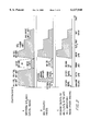
- FIG. 2 is a graph showing comparative temperature profiles and steps of two prior art processes for fabricating photovoltaic devices and the preferred method of the present invention.
- FIG. 3 is a graph showing temperature profiles and steps of an alternative embodiment of the present invention.
- FIG. 4 is a graph showing temperature profiles and steps of a second alternative embodiment of the present invention.
- FIG. 5 is a graph of current versus voltage for a photovoltaic device of the present invention.
- FIG. 1 shows cross-sectional views of two photovoltaic devices--one of the prior art and one of the improved device of the present invention.
- the prior art and inventive devices generally referred to by reference numerals 20 and 22, respectively, each contain a transparent substrate 24 through which radiant energy enters the device.
- the substrate can be made of any transparent material that can withstand the processing temperatures employed, such as glass, silica, or quartz.
- a thin transparent conductive oxide (TCO) film 25 is deposited onto the transparent substrate.
- the TCO layer is tin oxide or indium tin oxide (ITO), while in the present invention the TCO layer is cadmium stannate.
- Cadmium stannate TCO layers have numerous advantages including superior electrical, optical, and mechanical properties and stability at elevated temperatures, as described in our previous application U.S. Ser. No. 08/746,798.
- Each device includes an insulating buffer layer 26 atop the TCO layer, which in the prior art is also an insulating tin oxide film and in the present invention is zinc stannate.
- the cadmium stannate layer 25 is deposited between the transparent substrate 24 and the buffer layer 26 to serve as a front contact current collector, thus replacing the conventional TCO films commonly used in photovoltaic devices.
- a first semiconductor layer 28 is deposited upon the buffer layer 26 and a second semiconductor layer 30 is deposited upon the first semiconductor layer to form a heterojunction.
- the first semiconductor layer is preferably of CdS and can be termed a "window" layer 28.
- This term will be used hereafter in this application, as this layer is transparent to a large portion of the electromagnetic energy entering from the transparent substrate.
- the CdS layer in the prior art device is deposited at about 500°-600° C. by CSS techniques or in liquid solution by chemical bath deposition (CBD) at about 100° C.
- the CdS layer is applied by RF sputtering at ambient temperature.
- ambient or room temperature it is meant that the sputtered layer is applied at a temperature which is not elevated, but is normal in the laboratory or manufacturing facility, e.g. less than about 40° C.
- the conductivities of the first and second semiconductor layers are not the same. Both devices are shown with a second semiconductor layer of CdTe, as this material has highly desirable properties.
- the present invention can also be practiced using other semiconductor material combinations, such as amorphous silicon and polycrystalline thin-film silicon.
- a back electrical contact 34 is applied to the second semiconductor layer of CdTe or other material and is in ohmic contact therewith.
- Back electrical contacts can be of metal, semicondutor, or combination thereof, e.g. gold, ZnTe or nickel, or other suitable conductive materials, such as an HgTe-doped graphite paste.
- the devices 20 and 22 can include a front electrical contact 32 on the TCO film 25, the function and construction of which is known in the art and not a part of this invention.
- substrate 24 must be optically transparent over the range of light wavelengths for which transmission through the substrate is desired. Also, substrate 24 must be of a material capable of withstanding heat treatment at temperatures of 500° C. or more, as described below, and the TCO film 25, normally of cadmium stannate, must adhere to the substrate 24 material. The thermal expansion coefficient of the substrate 24 material must be close enough to that of the TCO film 25 and the semiconductor layers to prevent cracking or buckling of these films during heat treatment.
- an anti-reflective coating can be applied to the outer surface of substrate 24, using known materials such as MgF 2 .
- the TCO layer 25 can comprise any suitable transparent conductive oxide material known in the art, such as tin oxide, indium oxide, indium tin oxide (ITO), zinc oxide or cadmium stannate. Because of its properties and its ambient temperature method of deposition, cadmium stannate is preferred. Compared with the conventional tin oxide TCO films, cadmium stannate films are more conductive, more transparent, smoother (i.e., have lower surface roughness) and are exceptionally stable to elevated temperatures. The preferred method of depositing cadmium stannate by RF sputtering at ambient temperatures is described in our application U.S. Ser. No. 08/746,798. The process is normally carried out in an oxygen atmosphere.
- the TCO layer 25 of cadmium stannate is deposited by RF sputtering at ambient temperature.
- the cadmium stannate typically is applied in amorphous form.
- a buffer layer 26 of zinc stannate is deposited, also by RF sputtering at ambient temperature in an oxygen atmosphere, as described in detail in our application Ser. No. 09/149,430.
- the zinc stannate is also applied in amorphous form, and is later recrystallized.
- such zinc stannate layers provide a wider bandgap, higher transparency, high resistivity (comparable to that of the CdS film) and excellent chemical stability.
- a window layer 28 of CdS is normally applied next, preferably also by RF sputtering at ambient temperature in an argon atmosphere.
- the CdS layer can be deposited by close-space sublimination at a suitable temperature, e.g. 500°-600° C.
- a thin layer of CdTe or other semiconductor 30 is then deposited upon the window layer of CdS to form a heterojunction.
- the CdTe layer is applied by close-space sublimation at a temperature of at least about 500° C. The resulting temperature profile is effective to convert the cadmium stannate TCO layer to a single-phase spinel crystal structure with improved electrical and optical properties, and also to convert the zinc stannate buffer layer to a polycrystalline form.
- the CdTe layer can be deposited at lower temperatures, i.e. from about ambient temperature to about 550° C., by processes such as electrodeposition, screen printing, sputtering, spraying or physical vapor deposition (PVD), followed by heat treatment of the device at a temperature in the range of from about 500° to about 630° C., which treatment is also effective to crystallize the layers of cadmium stannate and zinc stannate.
- PVD physical vapor deposition
- the back electrical contact is applied to the device by any suitable method, such as evaporating, sputtering or screen printing.
- FIG. 2 illustrates temperature-time profiles for three processes of fabricating CdS/CdTe photovoltaic cells.
- FIG. 2A is a conventional process for producing a cell with a tin oxide TCO layer.
- FIG. 2B is the process of our previous application Ser. No. 09/149,430, and
- FIG. 2C is the preferred process for fabricating a cell using a cadmium stannate TCO layer, zinc stannate buffer layer, and cadmimum sulfide window layer, applying the three initial layers by RF sputtering at ambient temperature.
- the advantages of the temperature profile of this inventive process will be apparent upon inspection.
- FIG. 2A is a conventional process for producing a cell with a tin oxide TCO layer.
- FIG. 2B is the process of our previous application Ser. No. 09/149,430
- FIG. 2C is the preferred process for fabricating a cell using a cadmium stannate TCO layer, zinc stannate buffer
- tin oxide TCO and buffer layers are deposited by chemical vapor deposition (CVD) at temperatures of 500°-600° C.
- the letters "C" and "I” in FIG. 2A indicate conductive and insulating layers of tin oxide.
- a CdS semiconductor layer is deposited by either close-space sublimation at more than 500° C. or by chemical bath deposition at about 100° C.
- a CdTe semiconductor layer is deposited by close-space sublimation at 500°-630° C., followed by treatment with CdCl 2 vapor at about 400° C. and the application of the back contact at about 200°-300° C.
- the high temperatures required for the application of the tin oxide layers of FIG. 2A are largely eliminated by the depositing of cadmium stannate and zinc stannate as the TCO and buffer layers, respectively, except that the cadmium stannate requires annealing at 500°-630° C. for recrystallization before the zinc stannate is applied.
- the CdS semiconductor layer is deposited by chemical bath deposition at about 100° C., as can be done in the process of FIG. 2A. The final three steps are as described above for the process of FIG. 2A.
- the same layers of cadmium stannate, zinc stannate and cadmium sulfide are applied as in the process of FIG. 2B, but all three layers are preferably applied by RF sputtering at ambient temperature.
- the subsequent three steps of depositing CdTe by CSS, CdCl 2 treatment and application of a back contact are the same as in the processes of FIGS. 2A and 2B, except that the temperature profile of the CSS step itself is effective to convert the cadmium stannate TCO layer to a single phase spinel crystal structure. This eliminates the necessity of heating the cadmium stannate before the second step to recrystallize it.
- An additional optional step not shown is to anneal the first three layers in hydrogen at about 400° C. for removing oxides from the CdS surface before CdTe deposition.
- FIG. 3 illustrates an alternate procedure for the method of the invention.
- the first three layers of cadmium stannate, zinc stannate and CdS are applied by RF sputtering at ambient temperature as in FIG. 2C, but as the fourth step, the CdTe absorption layer is applied by a lower temperature (i.e. ambient temperature--550° C.,) process such as electrodeposition, screen printing, sputtering, PVD, or spraying.
- This step is followed by a heat treatment at about 500°-630° C. for a time effective to convert the amorphous cadmium stannate to the single-phase spinel crystal structure.
- the device is subjected to treatment in a CdCl 2 vapor at about 400° C., and the back contact is applied and annealed at a temperature of range of about 200°-300° C.
- the temperature profile for the final three steps of the process is similar to those in FIGS. 2A, 2B and 2C, except that the portions at elevated temperature are displaced to the right, i.e. delayed in time.
- FIG. 4 illustrates a second alternate version of the method of the invention.
- the CdS window layer is deposited by close-space sublimation at about 500°-600° C.
- the absorption layer of CdTe is then applied by close-space sublimation, preferably at a temperature range of about 500° C. to about 630° C.
- the device is then treated with CdCl 2 at about 400° C. and the back contact is applied and annealed at a temperature range of about 200°-300° C.
- the resistivity of cadmium stannate films is significantly lower (approximately two to six times lower) than that of conventional SnO 2 films deposited on similar substrates.
- the photovoltaic devices of the present invention offer the important advantage of reduced series resistance and increased fill factor, and hence improved efficiency, due to the presence of these low-resistivity cadmium stannate films.
- the TCO film is made too thick, decreased optical transmission may result.
- Another significant advantage associated with the photovoltaic device of the present invention is the improved optical transmission and electrical resistance of the cadmium stannate film, as compared to existing devices comprising conventional TCO films.
- conventional TCOs can have high inherent sheet resistances, which causes ohmic losses in the transparent conducting film and reduces the efficiency of the device.
- the thickness of the TCO layer must be increased, which decreases the optical transmission.
- the TCO can be deposited in a thin layer, thereby improving the optical transmission and hence the amount of electromagnetic radiation that reaches the semiconductor material.
- the photovoltaic device of the present invention with cadmium stannate TCO offers improved device short circuit currents, and hence improved performance.
- a yet further significant advantage of the photovoltaic device of the present invention is the improved surface morphology of the transparent conducting film which provides improved device performance.
- FIG. 4 of our previous application U.S. Ser. No. 08/746,798 provides a comparison of the surface morphologies of a conventional SnO 2 film (FIG. 4a) and a cadmium stannate film (FIG. 4b).
- FIG. 4 the surface of the cadmium stannate film is significantly smoother than the surface of the SnO 2 film.
- Data obtained from atomic force micrography (AFM) indicate that the average surface roughness of the cadmium stannate film is an order of magnitude lower than that of the SnO 2 film.
- AFM atomic force micrography
- the CdS film is either partially or completely consumed, forming a CdS 1-x Te x intermixed layer.
- the CdS consumption reportedly increases as the CdS film thickness decreases (B. E. McCandless and S. S. Hegedus, 22nd IEEE SPVC Proc. (1991) pp. 967-972).
- pinholes can develop and create TCO/CdTe junctions which reduces the open circuit voltage and fill factor.
- the probability of pinhole formation increases as the SnO 2 surface roughness increases (A. Rohatgi, et al., 22nd IEEE SPVC Proc. (1991) pp. 962-966).
- Cadmium stannate films are also much easier to pattern than conventional SnO 2 films (by etching in either HCl or HF), thus facilitating production and significantly expanding commercial applications.
- Patterned cadmium stannate films provide excellent edge definition, which is particularly important for certain commercial applications, such as in advanced photovoltaic module and flat panel display device processing.
- the photovoltaic device of the present invention is also more durable and stable (chemically and thermally) than existing devices due to the improved mechanical properties of the cadmium stannate film.
- cadmium stannate films deposited on glass substrates have good adhesion, are reasonably hard and scratch resistant, and exhibit high stability at elevated temperatures and over long periods of time.
- the cadmium stannate films are less affected by post-deposition processing (i.e., CdTe deposition or CdCl 2 heat-treatment) than conventional TCO films, thus improving process reproducibility and product yield.
- a significant advantage associated with the photovoltaic device of the present invention is the improved device performance due to the high resistivity and high transmittance of the zinc stannate film 26.
- the conversion efficiency of a heterojunction semiconductor device can be increased by reducing the window layer absorption, which increases short-circuit current (J sc ).
- J sc short-circuit current
- this is achieved by reducing the thickness of the CdS film to improve the blue spectral response.
- a relatively thin CdS film increases the probability of pinholes thereby forming localized TCO/CdTe junctions, which generally results in a reduced open-circuit voltage (V oc ) and fill factor.
- the CdS film is either partially or completely consumed forming a CdS 1-x Te x intermixed layer.
- the CdS consumption reportedly increases as the CdS film thickness decreases (B. E.) McChadless and S. S. Hegedus, 22nd IEEE SPVC Proc. (1991) pp. 967-972).
- additional pinholes can develop and create localized TCO/CdTe junctions, which reduce the open circuit voltage and fill factor.
- the photovoltaic device of the present invention minimizes these problems by including a zinc stannate film 26 between the TCO film 25 and the first semiconductor layer 28 (the CdS window layer). Because the resistivity of the zinc stannate film 26 matches the resistivity of the CdS window layer, the CdS film can be deposited in a thin layer without sacrificing open-circuit voltage (V oc ) and fill factor (F.F.).
- Zinc stannate films are not etched by strong acids (e.g., HCl, HNO 3 and nitric/phosphoric acid), thus are resistant to the chemicals used in conventional ohmic contact processing. Because the zinc stannate film functions as a "stop etch" protective buffer layer, the photovoltaic devices of the present invention are much less likely than conventional devices to short as a result of over etching.
- strong acids e.g., HCl, HNO 3 and nitric/phosphoric acid
- Another significant advantage associated with the photovoltaic device of the present invention is the improved mechanical properties due to the buffering effect of the zinc stannate buffer film.
- the zinc stannate films deposited on TCO-coated substrates have remarkably good adhesion and are less affected by CdCl 2 heat treatment than conventional photovoltaic devices, thus improving process reproducibility and product yield.
- a yet further significant advantage of the photovoltaic device of the present invention is the improved reproducibility in device performance as a result of the zinc stannate buffer film.
- FIG. 4 of our prior application Ser. No. 09/149,430 which shows the efficiency of 30 identically processed devices (18 Cd 2 SnO 4 -based CdTe cells and 12 SnO 2 -based CdTe cells), all of which included a zinc stannate film (no anti-reflection coating).
- the devices had an average efficiency of 13.83% with a standard deviation of 0.375.
- Photovoltaic devices as shown in FIG. 1 were fabricated by the method of FIG. 2C.
- Films of cadmium stannate (TCO), zinc stannate (buffer) and CdS (window) were all deposited by RF magnetron sputtering at room temperature (about 20°-40° C.).
- the sputtering was carried out in a modified CVC SC-3000 system, evacuated to a base pressure of about 1 ⁇ 10 -6 Torr and then backfilled with high purity oxygen (for cadmium stannate and zinc stannate films) or argon (for CdS film).
- Corning 7059 glass or soda-lime glass was placed in a sample holder parallel to the target surface.
- No antireflective coating was used on the substrates.
- the distance between the substrate and the target was varied from 6 to 9 cm.
- Commercial hot-press oxide targets were used in this work.
- Deposition was performed at a partial pressure of 10-20 ⁇ 10 -3 Torr, with the rf power between 50 and 150 watts.
- the electrical, optical and compositional properties of these films were characterized using Hall effect measurements, optical and infrared spectroscopy, X-ray diffraction (XRD), scanning electron microscopy (SEM) and atomic force microscopy (AFM).
- the device was annealed in hydrogen at 400° C. for 15 minutes. Following this annealing step, a CdTe film approximately 10 micrometers thick was deposited by close-space sublimation techniques. During deposition, the substrate and source temperatures were 625° C. and 660° C., respectively. The space between the substrate and the source was 0.2 cm. Deposition was initiated at a total pressure of 15 Torr in a He/O 2 ambient (14.5 Torr He, 0.5 Torr O 2 ). After CdTe deposition, the devices received a CdCl 2 vapor treatment at 400° C. for about 15 minutes in air. Finally, a HgTe-doped graphite paste back contact was applied to the devices.
- the preliminary device results of Examples 1-4 demonstrated that cells produced by the method of the present invention provide high open-circuit voltage, high fill factor and lower short-circuit current density values.
- the lower current density values can be attributed to the slightly lower transmission of the cadmium stannate TCO layers and the higher absorption of the thicker sputtered CdS films.
- the lower transmission of the cadmium stannate layers can be improved by modifying the temperature profile of the CdTe deposition step (namely, by post-thermal annealing of the first three layers).
- the higher absorption of the sputtered CdS layers can be reduced by reducing the thickness of the sputtered CdS layer through optimizing the thickness of the zinc stannate and cadmium stannate layers.
- CdS/CdTe cells with efficiencies approaching 14 percent can be produced by optimizing the process of the invention.
- CdS/CdTe thin-film solar cells are fabricated by the inventive alternate method of FIG. 3 and tested as described above. Electrical properties comparable to those of Examples 1-4 are obtained.
- CdS/CdTe thin-film solar cells are fabricated by the inventive alternate method of FIG. 4 and tested as described above. Electrical properties comparable to those of Examples 1-4 are obtained.
Landscapes
- Photovoltaic Devices (AREA)
Abstract
Description
              TABLE 1
______________________________________
Manu-                           CdS Window
  facturer TCO layer Buffer layer Layer
______________________________________
No. 1   CVD-SnO.sub.2
                   Sputtered I--SnO.sub.2
                                CSS-CdS
   550°-600° C. (for R & D) 550°-600° C.
                                 No. 2 CVD-SnO.sub.2 Spray-Cd-doped
                                Spray-CdS
   550°-600° C. SnO.sub.2 500°-550° C.
                                500-550° C.
  No. 3 CVD-SnO.sub.2 NA Electro-deposition-
   550°-600° C.  CdS ˜100° C.
  Present work RF sputtered RF sputtered RF sputtered
   Cd.sub.2 SnO.sub.4, RT Zn.sub.2 SnO.sub.4, RT CdS, RT
______________________________________
              TABLE 2
______________________________________
          Voc    Jsc         F.F.   Efficiency
  Example (mV) (mA/cm2) (percent) (percent)
______________________________________
1         820    20.9        70.5   12.1
  2 810 20.6 74.8 12.5
  3 814 20.7 72.8 12.3
  4 814 21.1 71.9 12.4
______________________________________
Claims (18)
Priority Applications (1)
| Application Number | Priority Date | Filing Date | Title |
|---|---|---|---|
| US09/218,206 US6137048A (en) | 1996-11-07 | 1998-12-22 | Process for fabricating polycrystalline semiconductor thin-film solar cells, and cells produced thereby |
Applications Claiming Priority (4)
| Application Number | Priority Date | Filing Date | Title |
|---|---|---|---|
| US08/740,347 US6221495B1 (en) | 1996-11-07 | 1996-11-07 | Thin transparent conducting films of cadmium stannate |
| US08/746,798 US5922142A (en) | 1996-11-07 | 1996-11-18 | Photovoltaic devices comprising cadmium stannate transparent conducting films and method for making |
| US09/149,430 US6169246B1 (en) | 1998-09-08 | 1998-09-08 | Photovoltaic devices comprising zinc stannate buffer layer and method for making |
| US09/218,206 US6137048A (en) | 1996-11-07 | 1998-12-22 | Process for fabricating polycrystalline semiconductor thin-film solar cells, and cells produced thereby |
Related Parent Applications (2)
| Application Number | Title | Priority Date | Filing Date |
|---|---|---|---|
| US08/746,798 Continuation-In-Part US5922142A (en) | 1996-11-07 | 1996-11-18 | Photovoltaic devices comprising cadmium stannate transparent conducting films and method for making |
| US09/149,430 Continuation-In-Part US6169246B1 (en) | 1996-11-07 | 1998-09-08 | Photovoltaic devices comprising zinc stannate buffer layer and method for making |
Publications (1)
| Publication Number | Publication Date |
|---|---|
| US6137048A true US6137048A (en) | 2000-10-24 |
Family
ID=27386830
Family Applications (1)
| Application Number | Title | Priority Date | Filing Date |
|---|---|---|---|
| US09/218,206 Expired - Lifetime US6137048A (en) | 1996-11-07 | 1998-12-22 | Process for fabricating polycrystalline semiconductor thin-film solar cells, and cells produced thereby |
Country Status (1)
| Country | Link |
|---|---|
| US (1) | US6137048A (en) |
Cited By (103)
| Publication number | Priority date | Publication date | Assignee | Title |
|---|---|---|---|---|
| US20030022471A1 (en) * | 1997-12-17 | 2003-01-30 | Matsushita Electric Industrial Co., Ltd. | Semiconductor thin film, method and apparatus for producing the same, and semiconductor device and method of producing the same |
| WO2003052837A1 (en) * | 2001-12-13 | 2003-06-26 | Midwest Research Institute | Semiconductor device with higher oxygen (o2) concentration within window layers and method for making |
| US6671026B2 (en) * | 2000-01-12 | 2003-12-30 | Schott Glas | Flat panel liquid-crystal display such as for a laptop computer |
| US6707526B2 (en) * | 2000-01-12 | 2004-03-16 | Schott Glas | Flat panel liquid crystal display such as for a laptop computer, having alkali-free aluminoborosilicate glass |
| US20040248340A1 (en) * | 2001-10-05 | 2004-12-09 | Nicola Romeo | Process for large-scale production of cdte/cds thin film solar cells |
| US20050257824A1 (en) * | 2004-05-24 | 2005-11-24 | Maltby Michael G | Photovoltaic cell including capping layer |
| US20060141266A1 (en) * | 2004-12-23 | 2006-06-29 | Industrial Technology Research Institute | Cadmium tin oxide multi-layer laminate and producing method thereof |
| US20070031593A1 (en) * | 2005-08-02 | 2007-02-08 | Alexey Krasnov | Method of thermally tempering coated article with transparent conductive oxide (TCO) coating using flame(s) in tempering furnace adjacent TCO to burn off oxygen and product made using same |
| US20070227587A1 (en) * | 2006-03-31 | 2007-10-04 | Walsh Kevin M | Photoelectric Cells Utilizing Accumulation Barriers For Charge Transport |
| EP1938964A1 (en) | 2006-12-29 | 2008-07-02 | E.I. Du Pont De Nemours And Company | Intrusion resistant safety glazings and solar cell modules |
| US20090078318A1 (en) * | 2007-09-25 | 2009-03-26 | First Solar, Inc. | Photovoltaic Devices Including An Interfacial Layer |
| WO2009043725A3 (en) * | 2007-10-04 | 2009-06-11 | Carlo Taliani | Process for preparing a solar cell |
| US20090194165A1 (en) * | 2008-01-31 | 2009-08-06 | Primestar Solar, Inc. | Ultra-high current density cadmium telluride photovoltaic modules |
| WO2009116990A1 (en) * | 2008-03-17 | 2009-09-24 | Midwest Research Institute | High quality transparent conducting oxide thin films |
| US20090242030A1 (en) * | 2008-03-26 | 2009-10-01 | E. I. Du Pont De Nemours And Company | High performance anti-spall laminate article |
| US20090250100A1 (en) * | 2008-04-04 | 2009-10-08 | E.I. Du Pont De Nemours And Company | Solar cell modules comprising high melt flow poly(vinyl butyral) encapsulants |
| US20090288701A1 (en) * | 2008-05-23 | 2009-11-26 | E.I.Du Pont De Nemours And Company | Solar cell laminates having colored multi-layer encapsulant sheets |
| US20100101647A1 (en) * | 2008-10-24 | 2010-04-29 | E.I. Du Pont De Nemours And Company | Non-autoclave lamination process for manufacturing solar cell modules |
| US20100129665A1 (en) * | 2008-11-24 | 2010-05-27 | E.I. Du Pont De Nemours And Company | Laminated articles comprising a sheet of a blend of ethylene copolymers |
| US20100154867A1 (en) * | 2008-12-19 | 2010-06-24 | E. I. Du Pont De Nemours And Company | Mechanically reliable solar cell modules |
| US20100163099A1 (en) * | 2008-12-31 | 2010-07-01 | E. I. Du Pont De Nemours And Company | Solar cell modules comprising encapsulant sheets with low haze and high moisture resistance |
| US20100180943A1 (en) * | 2009-01-22 | 2010-07-22 | E. I. Du Pont De Nemours And Company | Poly(vinyl butyral) encapsulant comprising chelating agents for solar cell modules |
| US20100186815A1 (en) * | 2009-01-29 | 2010-07-29 | First Solar, Inc. | Photovoltaic Device With Improved Crystal Orientation |
| US20100200063A1 (en) * | 2009-02-12 | 2010-08-12 | Derek Djeu | Thin film solar cell |
| US20100243437A1 (en) * | 2009-03-25 | 2010-09-30 | Alliance For Sustainable Energy, Llc | Research-scale, cadmium telluride (cdte) device development platform |
| US20100288354A1 (en) * | 2009-05-18 | 2010-11-18 | First Solar, Inc. | Cadmium stannate tco structure with diffusion barrier layer and separation layer |
| US20100319775A1 (en) * | 2009-06-22 | 2010-12-23 | First Solar, Inc. | Method and Apparatus for Annealing a Deposited Cadmium Stannate Layer |
| US20110023943A1 (en) * | 2009-07-31 | 2011-02-03 | E. I. Du Pont De Nemours And Company | Cross-linkable encapsulants for photovoltaic cells |
| US20110083972A1 (en) * | 2009-10-08 | 2011-04-14 | First Solar, Inc. | Electrochemical method and apparatus for removing coating from a substrate |
| US7939363B1 (en) * | 2010-10-27 | 2011-05-10 | General Electric Company | Systems and methods of intermixing cadmium sulfide layers and cadmium telluride layers for thin film photovoltaic devices |
| US7943415B1 (en) | 2010-10-27 | 2011-05-17 | Primestar Solar Inc. | Methods of sputtering cadmium sulfide layers for use in cadmium telluride based thin film photovoltaic devices |
| US20110136287A1 (en) * | 2008-06-06 | 2011-06-09 | Ii-Vi Incorporated | ANNEALING OF SEMI-INSULATING CdZnTe CRYSTALS |
| US20110143490A1 (en) * | 2009-12-15 | 2011-06-16 | Primestar Solar, Inc. | Methods of manufacturing cadmium telluride thin film photovoltaic devices |
| US20110139246A1 (en) * | 2009-12-16 | 2011-06-16 | Primestar Solar, Inc. | Methods for forming a transparent conductive oxide layer on a substrate |
| US20110147230A1 (en) * | 2009-12-18 | 2011-06-23 | First Solar, Inc. | Film Removal |
| WO2011075461A1 (en) * | 2009-12-18 | 2011-06-23 | First Solar, Inc. | Photovoltaic device back contact |
| CN102122581A (en) * | 2010-12-28 | 2011-07-13 | 福州大学 | Quantum dot sensitized zinc stannate nanocrystalline thin-film solar cell and preparation method thereof |
| WO2011084770A1 (en) * | 2009-12-21 | 2011-07-14 | Alion, Inc. | Methods for making thin film polycrystalline photovoltaic devices using additional chemical element and products thereof |
| CN102130207A (en) * | 2009-12-15 | 2011-07-20 | 初星太阳能公司 | Cadmium telluride thin film photovoltaic device and manufacturing method thereof |
| US20110197958A1 (en) * | 2010-02-12 | 2011-08-18 | Alliance For Sustainable Energy, Llc | Amorphous tin-cadmium oxide films and the production thereof |
| US20110227131A1 (en) * | 2010-03-18 | 2011-09-22 | Zhibo Zhao | Photovoltaic device with crystalline layer |
| US20110232758A1 (en) * | 2010-03-25 | 2011-09-29 | Rohm And Haas Electronic Materials Llc | Thin film photovoltaic cell |
| EP2371989A1 (en) * | 2010-03-30 | 2011-10-05 | PrimeStar Solar, Inc | Methods of forming a conductive transparent oxide film layer for use in a cadmium telluride based thin film photovoltaic device |
| CN102206801A (en) * | 2010-03-30 | 2011-10-05 | 初星太阳能公司 | Methods of forming a conductive transparent oxide film layer for use in a cadmium telluride based thin film photovoltaic device |
| CN102208485A (en) * | 2010-03-30 | 2011-10-05 | 初星太阳能公司 | Method of forming a conductive transparent oxide film layer for use in a cadmium telluride based thin film photovoltaic device |
| CN102208484A (en) * | 2010-03-30 | 2011-10-05 | 初星太阳能公司 | Methods of forming a conductive transparent oxide film layer for use in a cadmium telluride based thin film photovoltaic device |
| WO2011123117A1 (en) * | 2010-03-31 | 2011-10-06 | University Of Rochester | Photovoltaic cells with improved electrical contact |
| US20110240117A1 (en) * | 2010-04-02 | 2011-10-06 | Yu Yang | Photovoltaic device with transparent conducting layer |
| US20110259423A1 (en) * | 2010-04-22 | 2011-10-27 | General Electric Company | Methods for forming back contact electrodes for cadmium telluride photovoltaic cells |
| US20110259424A1 (en) * | 2010-04-21 | 2011-10-27 | EncoreSolar, Inc. | Method of fabricating solar cells with electrodeposited compound interface layers |
| EP2385151A1 (en) * | 2010-04-29 | 2011-11-09 | PrimeStar Solar, Inc | System and methods for high-rate co-sputtering of thin film layers on photovoltaic module substrates |
| US20110284078A1 (en) * | 2010-05-21 | 2011-11-24 | EncoreSolar, Inc. | Method of forming cadmium telluride thin film |
| US8080727B2 (en) | 2008-11-24 | 2011-12-20 | E. I. Du Pont De Nemours And Company | Solar cell modules comprising an encapsulant sheet of a blend of ethylene copolymers |
| US20110315209A1 (en) * | 2010-06-29 | 2011-12-29 | Primestar Solar | Selectively deposited thin film devices and methods for forming selectively deposited thin films |
| EP2403016A1 (en) * | 2010-07-02 | 2012-01-04 | PrimeStar Solar, Inc | Methods of forming a conductive transparent oxide film layer for use in a cadmium telluride based thin film photovoltaic device |
| US20120000768A1 (en) * | 2010-07-02 | 2012-01-05 | Primestar Solar, Inc. | Methods for sputtering a resistive transparent buffer thin film for use in cadmium telluride based photovoltaic devices |
| US20120012454A1 (en) * | 2010-07-15 | 2012-01-19 | National Taiwan University Of Science And Technology | Fabrication method of crystallized transparent conducting oxides on self-assembled organic layer modified substrate |
| DE202007019352U1 (en) | 2006-08-30 | 2012-01-31 | E.I. Du Pont De Nemours And Company | Solar cell modules comprising poly (allylamine) and poly (vinylamine) primed polyester films |
| WO2012016053A1 (en) | 2010-07-30 | 2012-02-02 | E. I. Du Pont De Nemours And Company | Cross-linkable ionomeric encapsulants for photovoltaic cells |
| WO2012021593A1 (en) * | 2010-08-13 | 2012-02-16 | First Solar, Inc. | Photovoltaic device with oxide layer |
| US20120067392A1 (en) * | 2010-09-22 | 2012-03-22 | Markus Gloeckler | Photovoltaic device containing an n-type dopant source |
| US8173482B2 (en) | 2010-04-30 | 2012-05-08 | Primestar Solar, Inc. | Devices and methods of protecting a cadmium sulfide for further processing |
| US8188562B2 (en) | 2011-05-31 | 2012-05-29 | Primestar Solar, Inc. | Multi-layer N-type stack for cadmium telluride based thin film photovoltaic devices and methods of making |
| US20120132261A1 (en) * | 2010-06-30 | 2012-05-31 | Benyamin Buller | Cadmium stannate sputter |
| EP2298032A4 (en) * | 2008-05-06 | 2012-06-20 | Agency Science Tech & Res | ELECTROCONDUCTIVE STRUCTURE FOR AN OPTICAL TRANSMITTER DEVICE |
| US20120174973A1 (en) * | 2009-09-30 | 2012-07-12 | Lg Innotek Co., Ltd. | Solar Cell Apparatus and Method For Manufacturing the Same |
| CN102593195A (en) * | 2010-11-30 | 2012-07-18 | 通用电气公司 | Electrode, photovoltaic device, and method of making |
| US20120192923A1 (en) * | 2011-02-01 | 2012-08-02 | General Electric Company | Photovoltaic device |
| US8236601B2 (en) | 2010-07-02 | 2012-08-07 | Primestar Solar, Inc. | Apparatus and methods of forming a conductive transparent oxide film layer for use in a cadmium telluride based thin film photovoltaic device |
| US8241930B2 (en) | 2011-05-31 | 2012-08-14 | Primestar Solar, Inc. | Methods of forming a window layer in a cadmium telluride based thin film photovoltaic device |
| US8247686B2 (en) | 2011-05-31 | 2012-08-21 | Primestar Solar, Inc. | Multi-layer N-type stack for cadmium telluride based thin film photovoltaic devices and methods of making |
| US8247682B2 (en) | 2010-06-29 | 2012-08-21 | Primestar Solar, Inc. | Metallic gridlines as front contacts of a cadmium telluride based thin film photovoltaic device |
| DE102012103243A1 (en) * | 2011-04-19 | 2012-10-25 | Primestar Solar, Inc. | Method for temporally varying the laser intensity during scoring of a photovoltaic device |
| US20120285375A1 (en) * | 2010-04-23 | 2012-11-15 | Primestar Solar, Inc. | Apparatus for treating thin film layers during photovoltaic module manufacture |
| US8349144B2 (en) | 2010-09-28 | 2013-01-08 | Primestar Solar, Inc. | Methods of sputtering using a non-bonded semiconducting target |
| US8354586B2 (en) | 2010-10-01 | 2013-01-15 | Guardian Industries Corp. | Transparent conductor film stack with cadmium stannate, corresponding photovoltaic device, and method of making same |
| US8399095B2 (en) | 2008-10-31 | 2013-03-19 | E I Du Pont De Nemours And Company | Solar cells modules comprising low haze encapsulants |
| US8445776B2 (en) | 2008-06-02 | 2013-05-21 | E I Du Pont De Nemours And Company | Solar cell module having a low haze encapsulant layer |
| US8460521B2 (en) | 2010-09-28 | 2013-06-11 | Primestar Solar, Inc. | Sputtering cathode having a non-bonded semiconducting target |
| US8476105B2 (en) | 2010-12-22 | 2013-07-02 | General Electric Company | Method of making a transparent conductive oxide layer and a photovoltaic device |
| US8525019B2 (en) | 2010-07-01 | 2013-09-03 | Primestar Solar, Inc. | Thin film article and method for forming a reduced conductive area in transparent conductive films for photovoltaic modules |
| US20130230945A1 (en) * | 2012-03-05 | 2013-09-05 | First Solar, Inc | Method and apparatus for forming a transparent conductive oxide using hydrogen |
| US20130252367A1 (en) * | 2012-03-26 | 2013-09-26 | Primestar Solar, Inc. | System and process for forming thin film photovoltaic device |
| US20130255779A1 (en) * | 2008-10-06 | 2013-10-03 | Corsam Technologies Llc | Intermediate thermal expansion coefficient glass |
| WO2013103730A3 (en) * | 2012-01-03 | 2013-12-19 | Heliovolt Corporation | Using amorphous zinc-tin oxide alloys in the emitter structure of cigs pv devices |
| EP2202803A3 (en) * | 2007-11-22 | 2014-01-22 | Antec Solar GmbH | CdS/CdTe modules with optimised efficiency |
| US8728855B2 (en) | 2012-09-28 | 2014-05-20 | First Solar, Inc. | Method of processing a semiconductor assembly |
| US8747630B2 (en) | 2007-01-16 | 2014-06-10 | Alliance For Sustainable Energy, Llc | Transparent conducting oxides and production thereof |
| WO2014100301A1 (en) | 2012-12-19 | 2014-06-26 | E. I. Du Pont De Nemours And Company | Cross-linked polymers and their use in photovoltaic modules |
| US8791356B2 (en) | 2010-07-23 | 2014-07-29 | First Solar, Inc. | Photovoltaic (PV) module with improved bus tape to foil ribbon contact |
| US9034686B2 (en) * | 2012-06-29 | 2015-05-19 | First Solar, Inc. | Manufacturing methods for semiconductor devices |
| US9054245B2 (en) | 2012-03-02 | 2015-06-09 | First Solar, Inc. | Doping an absorber layer of a photovoltaic device via diffusion from a window layer |
| US9093599B2 (en) | 2013-07-26 | 2015-07-28 | First Solar, Inc. | Vapor deposition apparatus for continuous deposition of multiple thin film layers on a substrate |
| US9117965B2 (en) * | 2011-10-28 | 2015-08-25 | Dow Global Technologies Llc | Method of manufacture of chalcogenide-based photovoltaic cells |
| WO2015171575A1 (en) | 2014-05-09 | 2015-11-12 | E. I. Du Pont De Nemours And Company | Encapsulant composition comprising a copolymer of ethylene, vinyl acetate and a third comonomer |
| US9276142B2 (en) | 2010-12-17 | 2016-03-01 | First Solar, Inc. | Methods for forming a transparent oxide layer for a photovoltaic device |
| US9496426B2 (en) | 2012-02-10 | 2016-11-15 | Alliance For Sustainable Energy, Llc | Thin film photovoltaic devices with a minimally conductive buffer layer |
| CN106299036A (en) * | 2016-11-23 | 2017-01-04 | 绍兴文理学院 | A kind of SnZnO cushion for solaode |
| US9643883B2 (en) | 2011-08-12 | 2017-05-09 | Corsam Technologies Llc | Fusion formable alkali-free intermediate thermal expansion coefficient glass |
| WO2019173262A1 (en) | 2018-03-08 | 2019-09-12 | E. I. Du Pont De Nemours And Company | Photovoltaic module and encapsulant composition having improved resistance to potential induced degradation |
| CN110835743A (en) * | 2018-08-17 | 2020-02-25 | 中智(泰兴)电力科技有限公司 | 9-cavity vertical HWCVD-PVD integrated equipment for solar cell manufacturing |
| US10651323B2 (en) | 2012-11-19 | 2020-05-12 | Alliance For Sustainable Energy, Llc | Devices and methods featuring the addition of refractory metals to contact interface layers |
| US12588297B2 (en) | 2021-06-01 | 2026-03-24 | First Solar, Inc. | Photovoltaic devices including an interfacial layer |
Citations (13)
| Publication number | Priority date | Publication date | Assignee | Title |
|---|---|---|---|---|
| US4231808A (en) * | 1978-09-05 | 1980-11-04 | Fuji Photo Film Co., Ltd. | Thin film photovoltaic cell and a method of manufacturing the same |
| US4445965A (en) * | 1980-12-01 | 1984-05-01 | Carnegie-Mellon University | Method for making thin film cadmium telluride and related semiconductors for solar cells |
| US4595791A (en) * | 1985-01-29 | 1986-06-17 | The Standard Oil Company | Thin-film photovoltaic devices incorporating current collector grid and method of making |
| US4595790A (en) * | 1984-12-28 | 1986-06-17 | Sohio Commercial Development Co. | Method of making current collector grid and materials therefor |
| US4596645A (en) * | 1984-10-23 | 1986-06-24 | California Institute Of Technology | Reactively-sputtered zinc semiconductor films of high conductivity for heterojunction devices |
| US4647711A (en) * | 1985-01-29 | 1987-03-03 | The Standard Oil Company | Stable front contact current collector for photovoltaic devices and method of making same |
| US4709466A (en) * | 1985-04-15 | 1987-12-01 | The University Of Delaware | Process for fabricating thin film photovoltaic solar cells |
| US5180476A (en) * | 1990-02-27 | 1993-01-19 | Nihon Shinku Gijutsu Kabushiki Kaisha | Method for producing transparent conductive films |
| US5261968A (en) * | 1992-01-13 | 1993-11-16 | Photon Energy, Inc. | Photovoltaic cell and method |
| US5304399A (en) * | 1990-09-11 | 1994-04-19 | Hitachi Chemical Co., Ltd. | Method of producing epoxy resin film |
| US5304499A (en) * | 1991-10-03 | 1994-04-19 | Battelle-Institut E.V. | Methods of making pn CdTe/CdS thin film solar cells |
| US5393675A (en) * | 1993-05-10 | 1995-02-28 | The University Of Toledo | Process for RF sputtering of cadmium telluride photovoltaic cell |
| US5714391A (en) * | 1995-05-17 | 1998-02-03 | Matsushita Electric Industrial Co., Ltd. | Method of manufacturing a compound semiconductor thin film for a photoelectric or solar cell device |
-
1998
- 1998-12-22 US US09/218,206 patent/US6137048A/en not_active Expired - Lifetime
Patent Citations (13)
| Publication number | Priority date | Publication date | Assignee | Title |
|---|---|---|---|---|
| US4231808A (en) * | 1978-09-05 | 1980-11-04 | Fuji Photo Film Co., Ltd. | Thin film photovoltaic cell and a method of manufacturing the same |
| US4445965A (en) * | 1980-12-01 | 1984-05-01 | Carnegie-Mellon University | Method for making thin film cadmium telluride and related semiconductors for solar cells |
| US4596645A (en) * | 1984-10-23 | 1986-06-24 | California Institute Of Technology | Reactively-sputtered zinc semiconductor films of high conductivity for heterojunction devices |
| US4595790A (en) * | 1984-12-28 | 1986-06-17 | Sohio Commercial Development Co. | Method of making current collector grid and materials therefor |
| US4595791A (en) * | 1985-01-29 | 1986-06-17 | The Standard Oil Company | Thin-film photovoltaic devices incorporating current collector grid and method of making |
| US4647711A (en) * | 1985-01-29 | 1987-03-03 | The Standard Oil Company | Stable front contact current collector for photovoltaic devices and method of making same |
| US4709466A (en) * | 1985-04-15 | 1987-12-01 | The University Of Delaware | Process for fabricating thin film photovoltaic solar cells |
| US5180476A (en) * | 1990-02-27 | 1993-01-19 | Nihon Shinku Gijutsu Kabushiki Kaisha | Method for producing transparent conductive films |
| US5304399A (en) * | 1990-09-11 | 1994-04-19 | Hitachi Chemical Co., Ltd. | Method of producing epoxy resin film |
| US5304499A (en) * | 1991-10-03 | 1994-04-19 | Battelle-Institut E.V. | Methods of making pn CdTe/CdS thin film solar cells |
| US5261968A (en) * | 1992-01-13 | 1993-11-16 | Photon Energy, Inc. | Photovoltaic cell and method |
| US5393675A (en) * | 1993-05-10 | 1995-02-28 | The University Of Toledo | Process for RF sputtering of cadmium telluride photovoltaic cell |
| US5714391A (en) * | 1995-05-17 | 1998-02-03 | Matsushita Electric Industrial Co., Ltd. | Method of manufacturing a compound semiconductor thin film for a photoelectric or solar cell device |
Non-Patent Citations (6)
| Title |
|---|
| Wu X.; Sheldon, P.; Mahathongdy, Y.; Ribelin, R.; Mason, A.; Moutinho, H.R.; Coutts, T.J.; CdS/CdTe Thin Film Solar Cell with a Zinc Stannate Buffer Layer , NREL, Department of Energy, Oct. 1998. * |
| Wu X.; Sheldon, P.; Mahathongdy, Y.; Ribelin, R.; Mason, A.; Moutinho, H.R.; Coutts, T.J.; CdS/CdTe Thin-Film Solar Cell with a Zinc Stannate Buffer Layer, NREL, Department of Energy, Oct. 1998. |
| Wu, X.; Sheldon, P.; Coutts, T.J.; Rose D.H.; Moutinho, H.R.; Application of Cd2SnO4 Transparent Conducting Oxides in Cd2S/CdTe Thin Film Devices , NREL, Department of Energy, 26th PVSD, pp. 347 350, Sep. 30 Oct. 3, 1997. * |
| Wu, X.; Sheldon, P.; Coutts, T.J.; Rose D.H.; Moutinho, H.R.; Application of Cd2SnO4 Transparent Conducting Oxides in Cd2S/CdTe Thin-Film Devices, NREL, Department of Energy, 26th PVSD, pp. 347-350, Sep. 30-Oct. 3, 1997. |
| Wu, X.; Sheldon, P.; Coutts, T.J.; Rose, D.H.; Mulligan, W.P.; Moutinho, H.R.; CP394, NREL, Department of Energy, Photovoltaics Program Review, CdS/CdTe Thin Film Devices Using a Cd2SnO4 Transparent Conducting Oxide , pp 693 702, AIP Press, 1997. * |
| Wu, X.; Sheldon, P.; Coutts, T.J.; Rose, D.H.; Mulligan, W.P.; Moutinho, H.R.; CP394, NREL, Department of Energy, Photovoltaics Program Review, CdS/CdTe Thin-Film Devices Using a Cd2SnO4 Transparent Conducting Oxide, pp 693-702, AIP Press, 1997. |
Cited By (171)
| Publication number | Priority date | Publication date | Assignee | Title |
|---|---|---|---|---|
| US6528397B1 (en) * | 1997-12-17 | 2003-03-04 | Matsushita Electric Industrial Co., Ltd. | Semiconductor thin film, method of producing the same, apparatus for producing the same, semiconductor device and method of producing the same |
| US20030022471A1 (en) * | 1997-12-17 | 2003-01-30 | Matsushita Electric Industrial Co., Ltd. | Semiconductor thin film, method and apparatus for producing the same, and semiconductor device and method of producing the same |
| US6806498B2 (en) | 1997-12-17 | 2004-10-19 | Matsushita Electric Industrial Co., Ltd. | Semiconductor thin film, method and apparatus for producing the same, and semiconductor device and method of producing the same |
| US6671026B2 (en) * | 2000-01-12 | 2003-12-30 | Schott Glas | Flat panel liquid-crystal display such as for a laptop computer |
| US6707526B2 (en) * | 2000-01-12 | 2004-03-16 | Schott Glas | Flat panel liquid crystal display such as for a laptop computer, having alkali-free aluminoborosilicate glass |
| US7211462B2 (en) * | 2001-10-05 | 2007-05-01 | Solar Systems & Equipments S.R.L. | Process for large-scale production of CdTe/CdS thin film solar cells |
| US20040248340A1 (en) * | 2001-10-05 | 2004-12-09 | Nicola Romeo | Process for large-scale production of cdte/cds thin film solar cells |
| US20050009228A1 (en) * | 2001-12-13 | 2005-01-13 | Xuanzhi Wu | Semiconductor device with higher oxygen (02) concentration within window layers and method for making |
| WO2003052837A1 (en) * | 2001-12-13 | 2003-06-26 | Midwest Research Institute | Semiconductor device with higher oxygen (o2) concentration within window layers and method for making |
| US20050257824A1 (en) * | 2004-05-24 | 2005-11-24 | Maltby Michael G | Photovoltaic cell including capping layer |
| AU2005330568B2 (en) * | 2004-05-24 | 2011-12-08 | First Solar, Inc. | Photovoltaic cell including capping layer |
| US20060141266A1 (en) * | 2004-12-23 | 2006-06-29 | Industrial Technology Research Institute | Cadmium tin oxide multi-layer laminate and producing method thereof |
| US7648783B2 (en) * | 2004-12-23 | 2010-01-19 | Industrial Research Technology Institute | Cadmium tin oxide multi-layer laminate and producing method thereof |
| US20070031593A1 (en) * | 2005-08-02 | 2007-02-08 | Alexey Krasnov | Method of thermally tempering coated article with transparent conductive oxide (TCO) coating using flame(s) in tempering furnace adjacent TCO to burn off oxygen and product made using same |
| US7744955B2 (en) * | 2005-08-02 | 2010-06-29 | Guardian Industries Corp. | Method of thermally tempering coated article with transparent conductive oxide (TCO) coating using flame(s) in tempering furnace adjacent TCO to burn off oxygen and product made using same |
| US20070227587A1 (en) * | 2006-03-31 | 2007-10-04 | Walsh Kevin M | Photoelectric Cells Utilizing Accumulation Barriers For Charge Transport |
| DE202007019352U1 (en) | 2006-08-30 | 2012-01-31 | E.I. Du Pont De Nemours And Company | Solar cell modules comprising poly (allylamine) and poly (vinylamine) primed polyester films |
| EP2286994A1 (en) | 2006-12-29 | 2011-02-23 | E. I. du Pont de Nemours and Company | Intrusion resistant safety glazings and solar cell modules |
| EP1938964A1 (en) | 2006-12-29 | 2008-07-02 | E.I. Du Pont De Nemours And Company | Intrusion resistant safety glazings and solar cell modules |
| US8747630B2 (en) | 2007-01-16 | 2014-06-10 | Alliance For Sustainable Energy, Llc | Transparent conducting oxides and production thereof |
| KR101503557B1 (en) | 2007-09-25 | 2015-03-17 | 퍼스트 솔라, 인코포레이티드 | Photovoltaic devices including an interfacial layer |
| WO2009045293A3 (en) * | 2007-09-25 | 2009-05-28 | First Solar Inc | Photovoltaic devices including an interfacial layer |
| US20090078318A1 (en) * | 2007-09-25 | 2009-03-26 | First Solar, Inc. | Photovoltaic Devices Including An Interfacial Layer |
| US20100282320A1 (en) * | 2007-09-25 | 2010-11-11 | First Solar, Inc. | Photovoltaic Devices Including an Interfacial Layer |
| WO2009043725A3 (en) * | 2007-10-04 | 2009-06-11 | Carlo Taliani | Process for preparing a solar cell |
| US20100282319A1 (en) * | 2007-10-04 | 2010-11-11 | Carlo Taliani | Process for Preparing a Solar Cell |
| US8343797B2 (en) | 2007-10-04 | 2013-01-01 | Carlo Taliani | Process for preparing a solar cell |
| CN101884119B (en) * | 2007-10-04 | 2013-09-25 | 卡洛·塔利亚尼 | Method for making solar cells |
| EP2202803A3 (en) * | 2007-11-22 | 2014-01-22 | Antec Solar GmbH | CdS/CdTe modules with optimised efficiency |
| US20090194165A1 (en) * | 2008-01-31 | 2009-08-06 | Primestar Solar, Inc. | Ultra-high current density cadmium telluride photovoltaic modules |
| US8253012B2 (en) | 2008-03-17 | 2012-08-28 | Alliance For Sustainable Energy, Llc | High quality transparent conducting oxide thin films |
| US20100171082A1 (en) * | 2008-03-17 | 2010-07-08 | Alliance For Sustainable Energy , Llc | HIGH QUALITY DOPED ZnO THIN FILMS |
| WO2009116990A1 (en) * | 2008-03-17 | 2009-09-24 | Midwest Research Institute | High quality transparent conducting oxide thin films |
| US20090242030A1 (en) * | 2008-03-26 | 2009-10-01 | E. I. Du Pont De Nemours And Company | High performance anti-spall laminate article |
| US20090250100A1 (en) * | 2008-04-04 | 2009-10-08 | E.I. Du Pont De Nemours And Company | Solar cell modules comprising high melt flow poly(vinyl butyral) encapsulants |
| EP2298032A4 (en) * | 2008-05-06 | 2012-06-20 | Agency Science Tech & Res | ELECTROCONDUCTIVE STRUCTURE FOR AN OPTICAL TRANSMITTER DEVICE |
| US20090288701A1 (en) * | 2008-05-23 | 2009-11-26 | E.I.Du Pont De Nemours And Company | Solar cell laminates having colored multi-layer encapsulant sheets |
| US8445776B2 (en) | 2008-06-02 | 2013-05-21 | E I Du Pont De Nemours And Company | Solar cell module having a low haze encapsulant layer |
| US8268663B2 (en) * | 2008-06-06 | 2012-09-18 | Ii-Vi Incorporated | Annealing of semi-insulating CdZnTe crystals |
| US20110136287A1 (en) * | 2008-06-06 | 2011-06-09 | Ii-Vi Incorporated | ANNEALING OF SEMI-INSULATING CdZnTe CRYSTALS |
| US20130255779A1 (en) * | 2008-10-06 | 2013-10-03 | Corsam Technologies Llc | Intermediate thermal expansion coefficient glass |
| US10196297B2 (en) | 2008-10-06 | 2019-02-05 | Corning, Incorporated | Intermediate thermal expansion coefficient glass |
| US9266769B2 (en) * | 2008-10-06 | 2016-02-23 | Corsam Technologies Llc | Intermediate thermal expansion coefficient glass |
| US20100101647A1 (en) * | 2008-10-24 | 2010-04-29 | E.I. Du Pont De Nemours And Company | Non-autoclave lamination process for manufacturing solar cell modules |
| US8399095B2 (en) | 2008-10-31 | 2013-03-19 | E I Du Pont De Nemours And Company | Solar cells modules comprising low haze encapsulants |
| US20100129665A1 (en) * | 2008-11-24 | 2010-05-27 | E.I. Du Pont De Nemours And Company | Laminated articles comprising a sheet of a blend of ethylene copolymers |
| US8084129B2 (en) | 2008-11-24 | 2011-12-27 | E. I. Du Pont De Nemours And Company | Laminated articles comprising a sheet of a blend of ethylene copolymers |
| US8080727B2 (en) | 2008-11-24 | 2011-12-20 | E. I. Du Pont De Nemours And Company | Solar cell modules comprising an encapsulant sheet of a blend of ethylene copolymers |
| WO2010080469A2 (en) | 2008-12-19 | 2010-07-15 | E. I. Du Pont De Nemours And Company | Mechanically reliable solar cell modules |
| US20100154867A1 (en) * | 2008-12-19 | 2010-06-24 | E. I. Du Pont De Nemours And Company | Mechanically reliable solar cell modules |
| US20100163099A1 (en) * | 2008-12-31 | 2010-07-01 | E. I. Du Pont De Nemours And Company | Solar cell modules comprising encapsulant sheets with low haze and high moisture resistance |
| US8399081B2 (en) | 2008-12-31 | 2013-03-19 | E I Du Pont De Nemours And Company | Solar cell modules comprising encapsulant sheets with low haze and high moisture resistance |
| US8338699B2 (en) | 2009-01-22 | 2012-12-25 | E I Du Pont De Nemours And Company | Poly(vinyl butyral) encapsulant comprising chelating agents for solar cell modules |
| US20100180943A1 (en) * | 2009-01-22 | 2010-07-22 | E. I. Du Pont De Nemours And Company | Poly(vinyl butyral) encapsulant comprising chelating agents for solar cell modules |
| CN102365707B (en) * | 2009-01-29 | 2015-02-04 | 第一太阳能有限公司 | Photovoltaic device with improved crystal orientation |
| US20100186815A1 (en) * | 2009-01-29 | 2010-07-29 | First Solar, Inc. | Photovoltaic Device With Improved Crystal Orientation |
| EP2392025A4 (en) * | 2009-01-29 | 2012-07-11 | First Solar Inc | PHOTOVOLTAIC DEVICE WITH ENHANCED CRYSTALLINE ORIENTATION |
| US20100200063A1 (en) * | 2009-02-12 | 2010-08-12 | Derek Djeu | Thin film solar cell |
| US20100243437A1 (en) * | 2009-03-25 | 2010-09-30 | Alliance For Sustainable Energy, Llc | Research-scale, cadmium telluride (cdte) device development platform |
| US20100288354A1 (en) * | 2009-05-18 | 2010-11-18 | First Solar, Inc. | Cadmium stannate tco structure with diffusion barrier layer and separation layer |
| EP2433307A4 (en) * | 2009-05-18 | 2012-10-31 | First Solar Inc | TCO STRUCTURE OF CADMIUM STANNATE WITH DIFFUSION STOP LAYER AND SEPARATION LAYER |
| JP2012531051A (en) * | 2009-06-22 | 2012-12-06 | ファースト ソーラー インコーポレイテッド | Method and apparatus for annealing deposited cadmium stannate layer |
| US20100319775A1 (en) * | 2009-06-22 | 2010-12-23 | First Solar, Inc. | Method and Apparatus for Annealing a Deposited Cadmium Stannate Layer |
| EP2446470A4 (en) * | 2009-06-22 | 2014-07-02 | First Solar Inc | METHOD AND APPARATUS FOR RECOVERING DEPOSITED CADMIUM STANNATE LAYER |
| US8609777B2 (en) | 2009-07-31 | 2013-12-17 | E I Du Pont De Nemours And Company | Cross-linkable encapsulants for photovoltaic cells |
| US20110023943A1 (en) * | 2009-07-31 | 2011-02-03 | E. I. Du Pont De Nemours And Company | Cross-linkable encapsulants for photovoltaic cells |
| US20120174973A1 (en) * | 2009-09-30 | 2012-07-12 | Lg Innotek Co., Ltd. | Solar Cell Apparatus and Method For Manufacturing the Same |
| US8779282B2 (en) * | 2009-09-30 | 2014-07-15 | Lg Innotek Co., Ltd. | Solar cell apparatus and method for manufacturing the same |
| US20110083972A1 (en) * | 2009-10-08 | 2011-04-14 | First Solar, Inc. | Electrochemical method and apparatus for removing coating from a substrate |
| US8252618B2 (en) | 2009-12-15 | 2012-08-28 | Primestar Solar, Inc. | Methods of manufacturing cadmium telluride thin film photovoltaic devices |
| US20110143490A1 (en) * | 2009-12-15 | 2011-06-16 | Primestar Solar, Inc. | Methods of manufacturing cadmium telluride thin film photovoltaic devices |
| US8143515B2 (en) | 2009-12-15 | 2012-03-27 | Primestar Solar, Inc. | Cadmium telluride thin film photovoltaic devices and methods of manufacturing the same |
| CN102130207A (en) * | 2009-12-15 | 2011-07-20 | 初星太阳能公司 | Cadmium telluride thin film photovoltaic device and manufacturing method thereof |
| US8303779B2 (en) | 2009-12-16 | 2012-11-06 | Primestar Solar, Inc. | Methods for forming a transparent conductive oxide layer on a substrate |
| US20110139246A1 (en) * | 2009-12-16 | 2011-06-16 | Primestar Solar, Inc. | Methods for forming a transparent conductive oxide layer on a substrate |
| US20110147230A1 (en) * | 2009-12-18 | 2011-06-23 | First Solar, Inc. | Film Removal |
| WO2011075461A1 (en) * | 2009-12-18 | 2011-06-23 | First Solar, Inc. | Photovoltaic device back contact |
| US20110146784A1 (en) * | 2009-12-18 | 2011-06-23 | First Solar, Inc. | Photovoltaic device back contact |
| WO2011084770A1 (en) * | 2009-12-21 | 2011-07-14 | Alion, Inc. | Methods for making thin film polycrystalline photovoltaic devices using additional chemical element and products thereof |
| US20110197958A1 (en) * | 2010-02-12 | 2011-08-18 | Alliance For Sustainable Energy, Llc | Amorphous tin-cadmium oxide films and the production thereof |
| US8568828B2 (en) | 2010-02-12 | 2013-10-29 | Alliance For Sustainable Energy, Llc | Amorphous tin-cadmium oxide films and the production thereof |
| WO2011116097A3 (en) * | 2010-03-18 | 2012-11-22 | First Solar, Inc | Photovoltaic device with crystalline layer |
| US8741687B2 (en) * | 2010-03-18 | 2014-06-03 | First Solar, Inc. | Photovoltaic device with crystalline layer |
| US20110227131A1 (en) * | 2010-03-18 | 2011-09-22 | Zhibo Zhao | Photovoltaic device with crystalline layer |
| CN103384919A (en) * | 2010-03-18 | 2013-11-06 | 第一太阳能有限公司 | Photovoltaic device with crystalline layer |
| US20110232758A1 (en) * | 2010-03-25 | 2011-09-29 | Rohm And Haas Electronic Materials Llc | Thin film photovoltaic cell |
| US8390122B2 (en) | 2010-03-30 | 2013-03-05 | Primestar Solar, Inc. | Sputtering targets including excess cadmium for forming a cadmium stannate layer |
| CN102208483B (en) * | 2010-03-30 | 2016-04-13 | 初星太阳能公司 | Form the method be used for based on the conductive transparent oxide rete of the thin-film photovoltaic device of cadmium telluride |
| US8043954B1 (en) | 2010-03-30 | 2011-10-25 | Primestar Solar, Inc. | Methods of forming a conductive transparent oxide film layer for use in a cadmium telluride based thin film photovoltaic device |
| US8043955B1 (en) | 2010-03-30 | 2011-10-25 | Primestar Solar, Inc. | Methods of forming a conductive transparent oxide film layer for use in a cadmium telluride based thin film photovoltaic device |
| CN102206801A (en) * | 2010-03-30 | 2011-10-05 | 初星太阳能公司 | Methods of forming a conductive transparent oxide film layer for use in a cadmium telluride based thin film photovoltaic device |
| CN102208483A (en) * | 2010-03-30 | 2011-10-05 | 初星太阳能公司 | Methods of forming a conductive transparent oxide film layer for use in a cadmium telluride based thin film photovoltaic device |
| CN102208484B (en) * | 2010-03-30 | 2016-09-21 | 初星太阳能公司 | The forming method of the conductive transparent oxide film layer used by film photovoltaic device based on cadmium telluride |
| US8053350B2 (en) | 2010-03-30 | 2011-11-08 | Primestar Solar, Inc | Methods of forming a conductive transparent oxide film layer for use in a cadmium telluride based thin film photovoltaic device |
| CN102208485B (en) * | 2010-03-30 | 2015-11-25 | 初星太阳能公司 | Based on the formation method of the film photovoltaic device of cadmium telluride conductive transparent oxide rete used |
| CN102208484A (en) * | 2010-03-30 | 2011-10-05 | 初星太阳能公司 | Methods of forming a conductive transparent oxide film layer for use in a cadmium telluride based thin film photovoltaic device |
| EP2371989A1 (en) * | 2010-03-30 | 2011-10-05 | PrimeStar Solar, Inc | Methods of forming a conductive transparent oxide film layer for use in a cadmium telluride based thin film photovoltaic device |
| CN102206801B (en) * | 2010-03-30 | 2016-08-03 | 初星太阳能公司 | The forming method of the conductive transparent oxide film layer used by film photovoltaic device based on cadmium telluride |
| CN102208485A (en) * | 2010-03-30 | 2011-10-05 | 初星太阳能公司 | Method of forming a conductive transparent oxide film layer for use in a cadmium telluride based thin film photovoltaic device |
| US8257561B2 (en) | 2010-03-30 | 2012-09-04 | Primestar Solar, Inc. | Methods of forming a conductive transparent oxide film layer for use in a cadmium telluride based thin film photovoltaic device |
| WO2011123117A1 (en) * | 2010-03-31 | 2011-10-06 | University Of Rochester | Photovoltaic cells with improved electrical contact |
| US20110240117A1 (en) * | 2010-04-02 | 2011-10-06 | Yu Yang | Photovoltaic device with transparent conducting layer |
| US8580603B2 (en) * | 2010-04-21 | 2013-11-12 | EncoreSolar, Inc. | Method of fabricating solar cells with electrodeposited compound interface layers |
| US20110259424A1 (en) * | 2010-04-21 | 2011-10-27 | EncoreSolar, Inc. | Method of fabricating solar cells with electrodeposited compound interface layers |
| US20110259423A1 (en) * | 2010-04-22 | 2011-10-27 | General Electric Company | Methods for forming back contact electrodes for cadmium telluride photovoltaic cells |
| US8524524B2 (en) * | 2010-04-22 | 2013-09-03 | General Electric Company | Methods for forming back contact electrodes for cadmium telluride photovoltaic cells |
| US9054241B2 (en) | 2010-04-22 | 2015-06-09 | First Solar, Inc. | Back contact electrodes for cadmium telluride photovoltaic cells |
| US20120285375A1 (en) * | 2010-04-23 | 2012-11-15 | Primestar Solar, Inc. | Apparatus for treating thin film layers during photovoltaic module manufacture |
| EP2385151A1 (en) * | 2010-04-29 | 2011-11-09 | PrimeStar Solar, Inc | System and methods for high-rate co-sputtering of thin film layers on photovoltaic module substrates |
| US8173482B2 (en) | 2010-04-30 | 2012-05-08 | Primestar Solar, Inc. | Devices and methods of protecting a cadmium sulfide for further processing |
| US20110284078A1 (en) * | 2010-05-21 | 2011-11-24 | EncoreSolar, Inc. | Method of forming cadmium telluride thin film |
| US8247682B2 (en) | 2010-06-29 | 2012-08-21 | Primestar Solar, Inc. | Metallic gridlines as front contacts of a cadmium telluride based thin film photovoltaic device |
| US8460765B2 (en) * | 2010-06-29 | 2013-06-11 | Primestar Solar, Inc. | Methods for forming selectively deposited thin films |
| US20110315209A1 (en) * | 2010-06-29 | 2011-12-29 | Primestar Solar | Selectively deposited thin film devices and methods for forming selectively deposited thin films |
| US20120132261A1 (en) * | 2010-06-30 | 2012-05-31 | Benyamin Buller | Cadmium stannate sputter |
| US8525019B2 (en) | 2010-07-01 | 2013-09-03 | Primestar Solar, Inc. | Thin film article and method for forming a reduced conductive area in transparent conductive films for photovoltaic modules |
| US8241938B2 (en) * | 2010-07-02 | 2012-08-14 | Primestar Solar, Inc. | Methods of forming a conductive transparent oxide film layer for use in a cadmium telluride based thin film photovoltaic device |
| EP2403016A1 (en) * | 2010-07-02 | 2012-01-04 | PrimeStar Solar, Inc | Methods of forming a conductive transparent oxide film layer for use in a cadmium telluride based thin film photovoltaic device |
| CN102315326B (en) * | 2010-07-02 | 2016-03-02 | 初星太阳能公司 | The formation method of the conductive transparent oxide rete used in cadmium telluride-based film photovoltaic device |
| US20120003784A1 (en) * | 2010-07-02 | 2012-01-05 | Primestar Solar, Inc. | Methods of forming a conductive transparent oxide film layer for use in a cadmium telluride based thin film photovoltaic device |
| US20120000768A1 (en) * | 2010-07-02 | 2012-01-05 | Primestar Solar, Inc. | Methods for sputtering a resistive transparent buffer thin film for use in cadmium telluride based photovoltaic devices |
| CN102315326A (en) * | 2010-07-02 | 2012-01-11 | 初星太阳能公司 | The formation method of the conductive, transparent oxide membranous layer that uses in the cadmium telluride-based film photovoltaic device |
| US8236601B2 (en) | 2010-07-02 | 2012-08-07 | Primestar Solar, Inc. | Apparatus and methods of forming a conductive transparent oxide film layer for use in a cadmium telluride based thin film photovoltaic device |
| US20120012454A1 (en) * | 2010-07-15 | 2012-01-19 | National Taiwan University Of Science And Technology | Fabrication method of crystallized transparent conducting oxides on self-assembled organic layer modified substrate |
| US8791356B2 (en) | 2010-07-23 | 2014-07-29 | First Solar, Inc. | Photovoltaic (PV) module with improved bus tape to foil ribbon contact |
| WO2012016053A1 (en) | 2010-07-30 | 2012-02-02 | E. I. Du Pont De Nemours And Company | Cross-linkable ionomeric encapsulants for photovoltaic cells |
| US8609980B2 (en) | 2010-07-30 | 2013-12-17 | E I Du Pont De Nemours And Company | Cross-linkable ionomeric encapsulants for photovoltaic cells |
| CN103180962A (en) * | 2010-08-13 | 2013-06-26 | 第一太阳能有限公司 | Photovoltaic device with oxide layer |
| US9640679B2 (en) | 2010-08-13 | 2017-05-02 | First Solar, Inc. | Photovoltaic device with oxide layer |
| WO2012021593A1 (en) * | 2010-08-13 | 2012-02-16 | First Solar, Inc. | Photovoltaic device with oxide layer |
| US9559247B2 (en) * | 2010-09-22 | 2017-01-31 | First Solar, Inc. | Photovoltaic device containing an N-type dopant source |
| US20120067392A1 (en) * | 2010-09-22 | 2012-03-22 | Markus Gloeckler | Photovoltaic device containing an n-type dopant source |
| US8349144B2 (en) | 2010-09-28 | 2013-01-08 | Primestar Solar, Inc. | Methods of sputtering using a non-bonded semiconducting target |
| US8460521B2 (en) | 2010-09-28 | 2013-06-11 | Primestar Solar, Inc. | Sputtering cathode having a non-bonded semiconducting target |
| US8354586B2 (en) | 2010-10-01 | 2013-01-15 | Guardian Industries Corp. | Transparent conductor film stack with cadmium stannate, corresponding photovoltaic device, and method of making same |
| US7939363B1 (en) * | 2010-10-27 | 2011-05-10 | General Electric Company | Systems and methods of intermixing cadmium sulfide layers and cadmium telluride layers for thin film photovoltaic devices |
| US7943415B1 (en) | 2010-10-27 | 2011-05-17 | Primestar Solar Inc. | Methods of sputtering cadmium sulfide layers for use in cadmium telluride based thin film photovoltaic devices |
| US8349084B2 (en) | 2010-10-27 | 2013-01-08 | General Electric Company | Apparatus and systems for intermixing cadmium sulfide layers and cadmium telluride layers for thin film photovoltaic devices |
| CN102593195A (en) * | 2010-11-30 | 2012-07-18 | 通用电气公司 | Electrode, photovoltaic device, and method of making |
| EP2472590A3 (en) * | 2010-11-30 | 2013-07-31 | General Electric Company | Electrode, photovoltaic device, and method of making |
| US9276142B2 (en) | 2010-12-17 | 2016-03-01 | First Solar, Inc. | Methods for forming a transparent oxide layer for a photovoltaic device |
| US8476105B2 (en) | 2010-12-22 | 2013-07-02 | General Electric Company | Method of making a transparent conductive oxide layer and a photovoltaic device |
| CN102122581B (en) * | 2010-12-28 | 2012-07-04 | 福州大学 | Preparation method of quantum dot sensitized zinc stannate nanocrystalline thin-film solar cell |
| CN102122581A (en) * | 2010-12-28 | 2011-07-13 | 福州大学 | Quantum dot sensitized zinc stannate nanocrystalline thin-film solar cell and preparation method thereof |
| US20120192923A1 (en) * | 2011-02-01 | 2012-08-02 | General Electric Company | Photovoltaic device |
| DE102012103243A1 (en) * | 2011-04-19 | 2012-10-25 | Primestar Solar, Inc. | Method for temporally varying the laser intensity during scoring of a photovoltaic device |
| DE102012103243B4 (en) * | 2011-04-19 | 2021-04-08 | First Solar Malaysia Sdn.Bhd | Method for changing the laser intensity over time during the scribing of a photovoltaic device |
| US8241930B2 (en) | 2011-05-31 | 2012-08-14 | Primestar Solar, Inc. | Methods of forming a window layer in a cadmium telluride based thin film photovoltaic device |
| US8247686B2 (en) | 2011-05-31 | 2012-08-21 | Primestar Solar, Inc. | Multi-layer N-type stack for cadmium telluride based thin film photovoltaic devices and methods of making |
| US8188562B2 (en) | 2011-05-31 | 2012-05-29 | Primestar Solar, Inc. | Multi-layer N-type stack for cadmium telluride based thin film photovoltaic devices and methods of making |
| US9643883B2 (en) | 2011-08-12 | 2017-05-09 | Corsam Technologies Llc | Fusion formable alkali-free intermediate thermal expansion coefficient glass |
| US9117965B2 (en) * | 2011-10-28 | 2015-08-25 | Dow Global Technologies Llc | Method of manufacture of chalcogenide-based photovoltaic cells |
| WO2013103730A3 (en) * | 2012-01-03 | 2013-12-19 | Heliovolt Corporation | Using amorphous zinc-tin oxide alloys in the emitter structure of cigs pv devices |
| US9496426B2 (en) | 2012-02-10 | 2016-11-15 | Alliance For Sustainable Energy, Llc | Thin film photovoltaic devices with a minimally conductive buffer layer |
| US9054245B2 (en) | 2012-03-02 | 2015-06-09 | First Solar, Inc. | Doping an absorber layer of a photovoltaic device via diffusion from a window layer |
| CN104334767A (en) * | 2012-03-05 | 2015-02-04 | 第一太阳能有限公司 | Method and apparatus for forming transparent conductive oxides using hydrogen |
| WO2013134127A1 (en) * | 2012-03-05 | 2013-09-12 | First Solar, Inc. | Method and apparatus for forming a transparent conductive oxide using hydrogen |
| CN104334767B (en) * | 2012-03-05 | 2017-06-09 | 第一太阳能有限公司 | Method and apparatus for forming transparent conductive oxides using hydrogen |
| US9236523B2 (en) * | 2012-03-05 | 2016-01-12 | First Solar, Inc | Method and apparatus for forming a transparent conductive oxide using hydrogen |
| US20130230945A1 (en) * | 2012-03-05 | 2013-09-05 | First Solar, Inc | Method and apparatus for forming a transparent conductive oxide using hydrogen |
| US20130252367A1 (en) * | 2012-03-26 | 2013-09-26 | Primestar Solar, Inc. | System and process for forming thin film photovoltaic device |
| US9034686B2 (en) * | 2012-06-29 | 2015-05-19 | First Solar, Inc. | Manufacturing methods for semiconductor devices |
| US8728855B2 (en) | 2012-09-28 | 2014-05-20 | First Solar, Inc. | Method of processing a semiconductor assembly |
| US10651323B2 (en) | 2012-11-19 | 2020-05-12 | Alliance For Sustainable Energy, Llc | Devices and methods featuring the addition of refractory metals to contact interface layers |
| WO2014100301A1 (en) | 2012-12-19 | 2014-06-26 | E. I. Du Pont De Nemours And Company | Cross-linked polymers and their use in photovoltaic modules |
| US9093599B2 (en) | 2013-07-26 | 2015-07-28 | First Solar, Inc. | Vapor deposition apparatus for continuous deposition of multiple thin film layers on a substrate |
| WO2015171575A1 (en) | 2014-05-09 | 2015-11-12 | E. I. Du Pont De Nemours And Company | Encapsulant composition comprising a copolymer of ethylene, vinyl acetate and a third comonomer |
| CN106299036A (en) * | 2016-11-23 | 2017-01-04 | 绍兴文理学院 | A kind of SnZnO cushion for solaode |
| WO2019173262A1 (en) | 2018-03-08 | 2019-09-12 | E. I. Du Pont De Nemours And Company | Photovoltaic module and encapsulant composition having improved resistance to potential induced degradation |
| CN110835743A (en) * | 2018-08-17 | 2020-02-25 | 中智(泰兴)电力科技有限公司 | 9-cavity vertical HWCVD-PVD integrated equipment for solar cell manufacturing |
| US12588297B2 (en) | 2021-06-01 | 2026-03-24 | First Solar, Inc. | Photovoltaic devices including an interfacial layer |
Similar Documents
| Publication | Publication Date | Title |
|---|---|---|
| US6137048A (en) | Process for fabricating polycrystalline semiconductor thin-film solar cells, and cells produced thereby | |
| US6169246B1 (en) | Photovoltaic devices comprising zinc stannate buffer layer and method for making | |
| US5922142A (en) | Photovoltaic devices comprising cadmium stannate transparent conducting films and method for making | |
| Compaan et al. | High efficiency, magnetron sputtered CdS/CdTe solar cells | |
| AU2011201197B2 (en) | Methods of forming a conductive transparent oxide film layer for use in a cadmium telluride based thin film photovoltaic device | |
| US20130133734A1 (en) | Photovoltaic cell | |
| CN102208483A (en) | Methods of forming a conductive transparent oxide film layer for use in a cadmium telluride based thin film photovoltaic device | |
| EP2383363B1 (en) | Cadmium sulfide layers for use in cadmium telluride based thin film photovoltaic devices and method of their manufacture | |
| US8303779B2 (en) | Methods for forming a transparent conductive oxide layer on a substrate | |
| CN102208485B (en) | Based on the formation method of the film photovoltaic device of cadmium telluride conductive transparent oxide rete used | |
| AU2011201273B2 (en) | Methods of forming a conductive transparent oxide film layer for use in a cadmium telluride based thin film photovoltaic device | |
| EP2403016B1 (en) | Methods of forming a conductive transparent oxide film layer for use in a cadmium telluride based thin film photovoltaic device | |
| CN102782860A (en) | Photovoltaic cell having a novel TCO layer built therein | |
| US8236601B2 (en) | Apparatus and methods of forming a conductive transparent oxide film layer for use in a cadmium telluride based thin film photovoltaic device | |
| Compaan | The status of and challenges in CdTe thin-film solar-cell technology | |
| JP2001223376A (en) | Manufacturing method for polycrystal semiconductor thin-film solar battery, and solar battery manufactured thereby | |
| Wu | FOR FABRICATING CdS/CdTe POLYCRYSTALLINE THIN-FILM SOLAR CELLS | |
| DE10003491A1 (en) | Preparation of thin film semiconductor layer on photovoltaic device for solar cell comprises forming cadmium stannate layer on substrate, forming zinc stannate layer, semiconducting window layer and second semiconducting layer and heating | |
| Naghavi | Contacts, Buffers, Substrates, and Interfaces | |
| Su et al. | CdTe thin film solar cell on flexible metallic substrate |
Legal Events
| Date | Code | Title | Description |
|---|---|---|---|
| AS | Assignment |
Owner name: MIDWEST RESEARCH INSTITUTE, MISSOURI Free format text: ASSIGNMENT OF ASSIGNORS INTEREST;ASSIGNORS:WU, XUANZHI;SHELDON, PETER;REEL/FRAME:009675/0752 Effective date: 19981222 |
|
| AS | Assignment |
Owner name: ENERGY, UNITED STATES DEPARTMENT OF, DISTRICT OF C Free format text: CONFIRMATORY LICENSE;ASSIGNOR:MIDWEST RESEARCH INSTITUTE;REEL/FRAME:010150/0276 Effective date: 19990706 |
|
| STCF | Information on status: patent grant |
Free format text: PATENTED CASE |
|
| FPAY | Fee payment |
Year of fee payment: 4 |
|
| FEPP | Fee payment procedure |
Free format text: PAT HOLDER NO LONGER CLAIMS SMALL ENTITY STATUS, ENTITY STATUS SET TO UNDISCOUNTED (ORIGINAL EVENT CODE: STOL); ENTITY STATUS OF PATENT OWNER: LARGE ENTITY |
|
| FPAY | Fee payment |
Year of fee payment: 8 |
|
| AS | Assignment |
Owner name: ALLIANCE FOR SUSTAINABLE ENERGY, LLC, COLORADO Free format text: ASSIGNMENT OF ASSIGNORS INTEREST;ASSIGNOR:MIDWEST RESEARCH INSTITUTE;REEL/FRAME:021603/0337 Effective date: 20080912 Owner name: ALLIANCE FOR SUSTAINABLE ENERGY, LLC,COLORADO Free format text: ASSIGNMENT OF ASSIGNORS INTEREST;ASSIGNOR:MIDWEST RESEARCH INSTITUTE;REEL/FRAME:021603/0337 Effective date: 20080912 |
|
| FPAY | Fee payment |
Year of fee payment: 12 |