EP0447850B1 - Method and apparatus for producing transparent conductive film - Google Patents
Method and apparatus for producing transparent conductive film Download PDFInfo
- Publication number
- EP0447850B1 EP0447850B1 EP91102978A EP91102978A EP0447850B1 EP 0447850 B1 EP0447850 B1 EP 0447850B1 EP 91102978 A EP91102978 A EP 91102978A EP 91102978 A EP91102978 A EP 91102978A EP 0447850 B1 EP0447850 B1 EP 0447850B1
- Authority
- EP
- European Patent Office
- Prior art keywords
- sputtering
- transparent conductive
- conductive film
- target
- electric field
- Prior art date
- Legal status (The legal status is an assumption and is not a legal conclusion. Google has not performed a legal analysis and makes no representation as to the accuracy of the status listed.)
- Expired - Lifetime
Links
- 238000000034 method Methods 0.000 title claims description 23
- 238000004544 sputter deposition Methods 0.000 claims description 83
- 230000005684 electric field Effects 0.000 claims description 33
- 239000000758 substrate Substances 0.000 claims description 29
- 229910052760 oxygen Inorganic materials 0.000 claims description 24
- 229910020923 Sn-O Inorganic materials 0.000 claims description 11
- 229910007541 Zn O Inorganic materials 0.000 claims description 6
- 230000015572 biosynthetic process Effects 0.000 claims description 2
- QVGXLLKOCUKJST-UHFFFAOYSA-N atomic oxygen Chemical compound [O] QVGXLLKOCUKJST-UHFFFAOYSA-N 0.000 description 19
- 239000001301 oxygen Substances 0.000 description 19
- 238000007599 discharging Methods 0.000 description 14
- 239000007789 gas Substances 0.000 description 12
- XKRFYHLGVUSROY-UHFFFAOYSA-N Argon Chemical compound [Ar] XKRFYHLGVUSROY-UHFFFAOYSA-N 0.000 description 10
- 150000001450 anions Chemical class 0.000 description 8
- 230000007423 decrease Effects 0.000 description 8
- 239000000203 mixture Substances 0.000 description 6
- 229910052786 argon Inorganic materials 0.000 description 5
- 238000001755 magnetron sputter deposition Methods 0.000 description 4
- XOLBLPGZBRYERU-UHFFFAOYSA-N tin dioxide Chemical compound O=[Sn]=O XOLBLPGZBRYERU-UHFFFAOYSA-N 0.000 description 4
- MYMOFIZGZYHOMD-UHFFFAOYSA-N Dioxygen Chemical compound O=O MYMOFIZGZYHOMD-UHFFFAOYSA-N 0.000 description 3
- 230000003247 decreasing effect Effects 0.000 description 3
- 229910001882 dioxygen Inorganic materials 0.000 description 3
- 238000002474 experimental method Methods 0.000 description 3
- 229910052738 indium Inorganic materials 0.000 description 3
- 229910052718 tin Inorganic materials 0.000 description 3
- 238000007796 conventional method Methods 0.000 description 2
- PJXISJQVUVHSOJ-UHFFFAOYSA-N indium(III) oxide Inorganic materials [O-2].[O-2].[O-2].[In+3].[In+3] PJXISJQVUVHSOJ-UHFFFAOYSA-N 0.000 description 2
- 239000011261 inert gas Substances 0.000 description 2
- 229920006395 saturated elastomer Polymers 0.000 description 2
- 239000011248 coating agent Substances 0.000 description 1
- 238000000576 coating method Methods 0.000 description 1
- 230000001419 dependent effect Effects 0.000 description 1
- 238000000151 deposition Methods 0.000 description 1
- 230000002542 deteriorative effect Effects 0.000 description 1
- 238000005530 etching Methods 0.000 description 1
- 238000010574 gas phase reaction Methods 0.000 description 1
- 239000011521 glass Substances 0.000 description 1
- 239000004973 liquid crystal related substance Substances 0.000 description 1
- 238000004519 manufacturing process Methods 0.000 description 1
- 239000000463 material Substances 0.000 description 1
- 239000011159 matrix material Substances 0.000 description 1
- 238000012986 modification Methods 0.000 description 1
- 230000004048 modification Effects 0.000 description 1
- 238000001771 vacuum deposition Methods 0.000 description 1
- 229910052725 zinc Inorganic materials 0.000 description 1
Images

Classifications
-
- C—CHEMISTRY; METALLURGY
- C23—COATING METALLIC MATERIAL; COATING MATERIAL WITH METALLIC MATERIAL; CHEMICAL SURFACE TREATMENT; DIFFUSION TREATMENT OF METALLIC MATERIAL; COATING BY VACUUM EVAPORATION, BY SPUTTERING, BY ION IMPLANTATION OR BY CHEMICAL VAPOUR DEPOSITION, IN GENERAL; INHIBITING CORROSION OF METALLIC MATERIAL OR INCRUSTATION IN GENERAL
- C23C—COATING METALLIC MATERIAL; COATING MATERIAL WITH METALLIC MATERIAL; SURFACE TREATMENT OF METALLIC MATERIAL BY DIFFUSION INTO THE SURFACE, BY CHEMICAL CONVERSION OR SUBSTITUTION; COATING BY VACUUM EVAPORATION, BY SPUTTERING, BY ION IMPLANTATION OR BY CHEMICAL VAPOUR DEPOSITION, IN GENERAL
- C23C14/00—Coating by vacuum evaporation, by sputtering or by ion implantation of the coating forming material
- C23C14/06—Coating by vacuum evaporation, by sputtering or by ion implantation of the coating forming material characterised by the coating material
- C23C14/08—Oxides
- C23C14/086—Oxides of zinc, germanium, cadmium, indium, tin, thallium or bismuth
-
- C—CHEMISTRY; METALLURGY
- C23—COATING METALLIC MATERIAL; COATING MATERIAL WITH METALLIC MATERIAL; CHEMICAL SURFACE TREATMENT; DIFFUSION TREATMENT OF METALLIC MATERIAL; COATING BY VACUUM EVAPORATION, BY SPUTTERING, BY ION IMPLANTATION OR BY CHEMICAL VAPOUR DEPOSITION, IN GENERAL; INHIBITING CORROSION OF METALLIC MATERIAL OR INCRUSTATION IN GENERAL
- C23C—COATING METALLIC MATERIAL; COATING MATERIAL WITH METALLIC MATERIAL; SURFACE TREATMENT OF METALLIC MATERIAL BY DIFFUSION INTO THE SURFACE, BY CHEMICAL CONVERSION OR SUBSTITUTION; COATING BY VACUUM EVAPORATION, BY SPUTTERING, BY ION IMPLANTATION OR BY CHEMICAL VAPOUR DEPOSITION, IN GENERAL
- C23C14/00—Coating by vacuum evaporation, by sputtering or by ion implantation of the coating forming material
- C23C14/06—Coating by vacuum evaporation, by sputtering or by ion implantation of the coating forming material characterised by the coating material
- C23C14/08—Oxides
-
- C—CHEMISTRY; METALLURGY
- C23—COATING METALLIC MATERIAL; COATING MATERIAL WITH METALLIC MATERIAL; CHEMICAL SURFACE TREATMENT; DIFFUSION TREATMENT OF METALLIC MATERIAL; COATING BY VACUUM EVAPORATION, BY SPUTTERING, BY ION IMPLANTATION OR BY CHEMICAL VAPOUR DEPOSITION, IN GENERAL; INHIBITING CORROSION OF METALLIC MATERIAL OR INCRUSTATION IN GENERAL
- C23C—COATING METALLIC MATERIAL; COATING MATERIAL WITH METALLIC MATERIAL; SURFACE TREATMENT OF METALLIC MATERIAL BY DIFFUSION INTO THE SURFACE, BY CHEMICAL CONVERSION OR SUBSTITUTION; COATING BY VACUUM EVAPORATION, BY SPUTTERING, BY ION IMPLANTATION OR BY CHEMICAL VAPOUR DEPOSITION, IN GENERAL
- C23C14/00—Coating by vacuum evaporation, by sputtering or by ion implantation of the coating forming material
- C23C14/22—Coating by vacuum evaporation, by sputtering or by ion implantation of the coating forming material characterised by the process of coating
- C23C14/34—Sputtering
- C23C14/35—Sputtering by application of a magnetic field, e.g. magnetron sputtering
-
- H—ELECTRICITY
- H01—ELECTRIC ELEMENTS
- H01L—SEMICONDUCTOR DEVICES NOT COVERED BY CLASS H10
- H01L31/00—Semiconductor devices sensitive to infrared radiation, light, electromagnetic radiation of shorter wavelength or corpuscular radiation and specially adapted either for the conversion of the energy of such radiation into electrical energy or for the control of electrical energy by such radiation; Processes or apparatus specially adapted for the manufacture or treatment thereof or of parts thereof; Details thereof
- H01L31/18—Processes or apparatus specially adapted for the manufacture or treatment of these devices or of parts thereof
- H01L31/1884—Manufacture of transparent electrodes, e.g. TCO, ITO
-
- Y—GENERAL TAGGING OF NEW TECHNOLOGICAL DEVELOPMENTS; GENERAL TAGGING OF CROSS-SECTIONAL TECHNOLOGIES SPANNING OVER SEVERAL SECTIONS OF THE IPC; TECHNICAL SUBJECTS COVERED BY FORMER USPC CROSS-REFERENCE ART COLLECTIONS [XRACs] AND DIGESTS
- Y02—TECHNOLOGIES OR APPLICATIONS FOR MITIGATION OR ADAPTATION AGAINST CLIMATE CHANGE
- Y02E—REDUCTION OF GREENHOUSE GAS [GHG] EMISSIONS, RELATED TO ENERGY GENERATION, TRANSMISSION OR DISTRIBUTION
- Y02E10/00—Energy generation through renewable energy sources
- Y02E10/50—Photovoltaic [PV] energy
Definitions
- This invention relates to a method and an apparatus for producing a transparent conductive film and in particular to a method and an apparatus for producing an In-O, Sn-O, Zn-O, Cd-Sn-O or Cd-In-O based transparent conductive film used as an electrode for a liquid crystal display element or the like and a solar battery or the like.
- the sputtering methods are superior to the other producing methods in that a transparent conductive film of relatively low electric resistance is easily obtained and that this transparent conductive film can be formed uniformly and well controllably on a large-sized substrate with a good reproducibility or repeatability.
- the magnetron sputtering method which utilizes plasma confinement by a magnetic field on a surface of a target is generally used because it has a large film-forming speed and is superior for mass production.
- a DC power supply is normally used because it is superior in points of cost, uniformity of electric discharging, film-forming speed or the like.
- the temperature of a substrate and the partial pressure of oxygen are known as factors which affect the electrical resistivity of the transparent conductive film.
- the substrate temperature it is known that the higher the substrate temperature, the lower the electrical resistivity of the resulting film.
- the partial pressure of oxygen it is known that in a region of lower oxygen partial pressure, the density of a carrier is larger, and the mobility is smaller because there are many vacancies of oxygen as a donor in such a region. Whereas in a region of higher oxygen partial pressure, the density of a carrier is smaller and the mobility is larger.
- the transparent electrode have a lower electric resistance because of enlargement of a display screen size.
- the prior art sputtering methods can no longer meet the requirements.
- a transparent conductive film is used in the scanning signal electrode. If the electric resistance of the transparent conductive film is high, the image quality is deteriorated. Therefore, the electric resistance of the transparent conductive film must be low.
- a transparent conductive film is normally formed on an organic color filter. Therefore, the temperature of forming the transparent conductive film is limited to about 160 to 200°C due to the heat-resisting temperature of the filter, and a requirement for forming the transparent conductive film at a lower temperature is getting stronger.
- a transparent oxide conductive film is formed by a sputtering method
- anions of oxygen are generated by ionization of oxygen in the introduced oxygen gas or a target composition.
- These anions smash into a substrate, thereby giving micro-damages to the transparent conductive film that is being formed and consequently deteriorating the film characteristics such as resistance or the like. Since these anions are accelerated by an electric field to be generated by the negative electric potential of the target, the degree to which the formed transparent conductive film is deteriorated is proportional to the energy of the anions, i.e., the negative electric potential of the target.
- the target during sputtering is understood to be in the negative electric potential and an absolute value thereof is called a sputtering voltage or a discharging voltage.
- the intensity of a magnetic field on the surface of the target was increased and the density of plasma by magnetron discharging was increased, resulting in a decrease or lowering in the electric discharging voltage.
- the target electric potential is -400V
- the electrical resistivity of the transparent conductive film at that time linearly dropped relative to the sputtering voltage within the sputtering voltage range of 400 to 250V. It was expected that the electrical resistivity would further lower also in the range of the sputtering voltage of 250V or below.
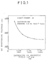
- Fig. 1 shows the relationship between the intensity of the magnetic field on the surface of the target and the discharging voltage during sputtering.
- the sputtering voltage effectively decreases with the increase in the intensity of the magnetic field.
- the decrease in the sputtering voltage is almost saturated, and the sputtering voltage becomes about 250V at 1.273 x 10 5 A/m (1600 Oe).
- the intensity of the magnetic field is further increased, the decrease in the sputtering voltage cannot be expected any more.
- this invention has an object, by eliminating the problems associated with the conventional methods, of providing a method of and an apparatus for producing a transparent conductive film with still lower electric resistance.
- the inventors of this invention Upon diligent studies to attain the above-described object, the inventors of this invention have found that the sputtering voltage can further be lowered or decreased by superimposing an RF electric field on a DC electric field for discharging purpose while, at the same time, increasing the intensity of the magnetic field on the surface of the target.
- This invention has been made on the basis of the above-described finding.
- This invention is a method of producing an In-O, Sn-O, Zn-O, Cd-Sn-O or Cd-In-O based transparent conductive film with an optional addition of a donor element, wherein the sputtering is carried out by maintaining an intensity of a magnetic field on a surface of a target at a level of 0.477 x 10 5 A/m (600 Oe) or greater and sputtering the target so as to form the transparent conductive film on a substrate by charging the target, simultaneously with said maintaining of the magnetic field intensity, with a DC electric field superimposed with an RF electric field so as to lower the sputtering voltage to 250 volts or less.
- the inventors of this invention succeeded in largely lowering the sputtering voltage below 250V by superimposing, as a means of increasing the density of plasma, the RF electric field on the DC electric field for generating the discharging.
- the superimposition of the RF electric field is effective when the intensity of the magnetic field on the surface of the target is 0.477 x 10 5 A/m (600 Oe) or more.
- the intensity of the magnetic field is below 0.477 x 10 5 A/m (600 Oe)
- the sputtering voltage contrarily increases by the superimposition of the RF electric field. Therefore, in superimposing the high-frequency electric filed, the intensity of the magnetic field on the surface of the target must be maintained at 0.477 x 10 5 A/m (600 Oe) or greater.
- an In, Sn, Zn, Cd-Sn, Cd-In based metallic target or the like or its sintered oxide based target with an addition, depending on necessity, of a donor element is used.
- Sn is generally used for an In-O based target
- Sb for an Sn-O based target
- In, Al, Si or the like for a Zn-O based target, respectively.
- the In-O based target with an addition of a small amount of Sn results in a film of the lowest resistance value. In addition, it is superior in the etching characteristics of the resultant film. It is therefore preferable to use the ITO target.
- the target may be of a sintered oxide target, and a DC power supply can be used as the electric discharging power supply because the sintered oxide target itself has a high electric conductivity.
- a mixture gas of an inert gas such, for example, as Ar or the like added by oxygen may be used.
- Ar is used as the inert gas, it is preferable to make the mixture gas pressure to the order of about 0.133 Pa (10 -3 Torr), and the oxygen partial pressure to the order of about 0.001 Pa (10 -5 Torr).
- Another aspect of this invention is an apparatus for producing an In-O, Sn-O, Zn-O, Cd-Sn-O or Cd-In-O based transparent conductive film with an optional addition of a donor element, the apparatus having a vacuum chamber adapted to support therein a substrate and a target in an opposed relationship to each other for forming by sputtering the transparent conductive film on the substrate by plasma discharge generated therebetween, wherein the apparatus comprises means for forming a magnetic field having a predetermined intensity of 0.477 x 10 5 A/m (600 Oe) or greater on a surface of the target, and power supply means for sputtering used in forming the transparent conductive film, said power supply means including DC power supply means for charging the target with a DC electric field, and RF power supply means for charging the target with a RF electric field superimposed on the DC electric field, said power supply means so constructed and arranged as to supply an electric field to the target by superimposing the RF electric field on the DC electric field while maintaining a sp
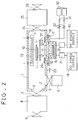
- Fig. 2 is a sectional view of an apparatus for producing a transparent conductive film according to one embodiment of this invention.
- numeral 1 denotes a vacuum chamber, i.e., a sputtering chamber.
- this sputtering chamber 1 there are provided three openings, i.e., an exhaust port 2, a loading port 3 and an unloading port 4.
- the exhaust port 2 is communicated with an evacuating means 6 such as a cryopump or the like via a valve 5 so that the sputtering chamber 1 can be adjusted in its vacuum degree by the evacuating means 6.
- an evacuating means 6 such as a cryopump or the like
- the loading port 3 is communicated with a loading chamber 8 via a valve 7.
- This loading chamber 8 is also provided at its loading port with a valve 9.
- the sputtering chamber 1 is communicated with a sputtering gas supply source 30, from which a sputter gas such, for example, as argon and oxygen is supplied independently or as a mixture gas through stop valves 31, mass flow controllers 32 and a nozzle 33.
- the partial pressures of the above-described argon gas and oxygen gas are respectively controlled for setting to the order, for example, of 0.113 Pa (10 -3 Torr) with argon gas and 0.001 Pa (10 -5 Torr) with oxygen gas.
- a substrate 11 supported on a substrate holder 10, and a sputter cathode 12.
- This substrate holder 10 is either fixed or so arranged as to be linearly movable inside the sputtering chamber 1 while maintaining a parallel relationship with the sputter cathode 12.
- a means for linearly driving the substrate holder as described above is also provided.
- a heater 13 to control the substrate temperature in the film-forming process to a predetermined temperature.
- the sputter cathode 12 is water-cooled, and on the front surface thereof there is fixed a target 14 with a brading material.
- a cathode case 17 which contains therein a permanent magnet 16 supported on a pole piece 15.
- This permanent magnet 16 is for generating a magnetic field for magnetron discharging.
- the intensity of the magnetic field on the surface of the target 14 is adjusted by varying the distance between the permanent magnet 16 and the target 14, the intensity of the magnetic field being made adjustable up to a maximum of 1.273 x 10 5 A/m (1600 Oe).
- a DC power supply means 19 as a main power supply and an RF (e.g., 13.56MHz) power supply means 20 as an auxiliary power supply are used.
- the DC power supply means 19 is connected, via an RF filter 21 for preventing the incoming RF electric field, and the RF power supply means 20 is connected via a matching box 22, respectively to the cathode case 17 and further to the sputter cathode 12.
- the sputtering chamber 1 is grounded as shown by numeral 23. It is thus so arranged that, by making the sputtering chamber 1 to be at earth potential, the cathode case 17 is charged with a negative voltage so that DC magnetron sputtering can be carried out inside the vacuum chamber 1.
- the unloading port 4 of the vacuum chamber 1 is communicated with an unloading chamber 25 via a valve 24.
- This unloading chamber 25 is also provided at its unloading port with a valve 26.
- the substrate 11 is mounted on the substrate holder 10 from the side of the loading chamber 8, and the substrate having formed a transparent conductive film on the surface thereof is unloaded from the side of the unloading chamber 25.
- numeral 27 denotes an anti-deposition plate and numeral 29 denotes an earth shield.
- a sintered target of In 2 O 3 with an addition of 10% by weight of SnO 2 was used.
- the distance between the target and the substrate was set at 80mm, and the intensity of the magnetic field was set at 1.273 x 10 5 A/m (1600 Oe), and the DC power supply was controlled to maintain a constant current supply of 2A.
- an RF electric field of 13.56MHz was superimposed, while varying the electric power, on the discharging by the DC electric field.
- the DC sputtering voltage at this time was measured.
- a sputtering gas as a sputtering gas, a mixture gas of argon and oxygen was introduced into the sputtering chamber 1, and the total pressure therein was adjusted to 0.8 Pa (6 x 10 -3 Torr).
- the results are shown in Fig. 3.
- the sputtering voltage lowered or decreased with an increase in the RF electric power when the high-frequency electric field was charged by superimposition.
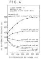
- the DC sputtering voltage was also measured when the intensity of the magnetic field was varied within the range of 0.238 x 10 5 and 1.273x10 5 A/m (300 and 1600 Oe) and, at the same time, when the RF electric field was charged by superimpostion while varying the electric power.
- the results are shown in Fig. 4. As can be seen from the graph of this figure, when the intensity of the magnetic field was 0.477x10 5 A/m (600 Oe) or greater, the DC sputtering voltage lowered by the superimposition of the RF electric field.
- the intensity of the magnetic field was 0.398 x 10 5 A/m (500 Oe) or below
- the sputtering voltage increased as a result of the superimposition of the RF electric field. Therefore, in order to lower the sputtering voltage by superimposing the RF electric field, the intensity of the magnetic field on the surface of the target must be maintained at 0.477 x 10 5 A/m (600 Oe) or greater.
- an oxide target 14 (125mm x 406mm in size) of In 2 O 3 with an addition of 10% by weight of SnO 2 and a substrate 11 made of a transparent glass (No. 7059 of Corning Co. make, 1.1mm in thickness).
- a sputtering gas a mixture gas of argon and oxygen was introduced into the sputtering chamber 1, and the total pressure therein was adjusted to 0.8 Pa (6 x 10 -3 Torr).
- the sputtering voltage was varied, in the range of 250V and more, only by varying the intensity of the magnetic field.
- the intensity of the magnetic field was 1.273 x 10 5 A/m (1600 Oe) at the sputtering voltage of 250V
- the sputtering voltage was varied in the range of 250V or less by superimposing the RF electric field while maintaining the intensity of the magnetic field at 1.273 x 10 5 A/m (1600 Oe).
- the electrical resistivity of the ITO film was measured by varying the partial pressure of oxygen in the order of 0.001 Pa (10 -5 Torr) under the respective conditions, and a most optimum value was selected.
- Film forming was carried out by moving the substrate from the side of the loading port 3 towards the side of the unloading port 4 at an equal speed, while maintaining the substrate temperature at 200°C under the above-described conditions.
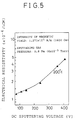
- Fig. 5 shows the relationship between the sputtering voltage and the electrical resistivity of the ITO film obtained.
- the electrical resistivities of the ITO film of as low as 1.9 x 10 -4 ⁇ cm at the sputtering voltage of 250V and 1.25 x 10 -4 ⁇ cm by still further lowering the voltage to 80V, as compared with 4.5 x 10 -4 ⁇ cm at the sputtering voltage of 420V.
- an SnO based or a ZnO based sintered body may also be used as well.
- the electric resistance is deteriorated by the incidence of the anions of oxygen or the like.
- the electrical resistivity of the formed transparent conductive film can be lowered by lowering the sputtering voltage, like in the case of using the above-described ITO based target.
Description
- This invention relates to a method and an apparatus for producing a transparent conductive film and in particular to a method and an apparatus for producing an In-O, Sn-O, Zn-O, Cd-Sn-O or Cd-In-O based transparent conductive film used as an electrode for a liquid crystal display element or the like and a solar battery or the like.
- There are conventionally known methods of producing this kind of transparent conductive film such as coating, vacuum deposition, and gas-phase reaction methods as well as sputtering methods including a DC or RF double-pole sputtering method and a DC or RF magnetron sputtering method. Among these producing methods, the sputtering methods are superior to the other producing methods in that a transparent conductive film of relatively low electric resistance is easily obtained and that this transparent conductive film can be formed uniformly and well controllably on a large-sized substrate with a good reproducibility or repeatability. Among the producing methods by these sputtering methods, the magnetron sputtering method which utilizes plasma confinement by a magnetic field on a surface of a target is generally used because it has a large film-forming speed and is superior for mass production. Further, as an electric power supply for generating electric discharging, a DC power supply is normally used because it is superior in points of cost, uniformity of electric discharging, film-forming speed or the like.
- In the method of producing a transparent conductive film by sputtering methods, the temperature of a substrate and the partial pressure of oxygen are known as factors which affect the electrical resistivity of the transparent conductive film. As regards the substrate temperature, it is known that the higher the substrate temperature, the lower the electrical resistivity of the resulting film. On the other hand, as regards the partial pressure of oxygen, it is known that in a region of lower oxygen partial pressure, the density of a carrier is larger, and the mobility is smaller because there are many vacancies of oxygen as a donor in such a region. Whereas in a region of higher oxygen partial pressure, the density of a carrier is smaller and the mobility is larger. Thus, there is an optimum partial pressure of oxygen that will result in an electrical resistivity of a minimum value from an even balance of the density and the mobility. Thus, it was a practice in the prior art sputtering methods to produce a transparent conductive film having a lower electrical resistivity wherein parameters of the substrate temperature and the partial pressure of oxygen were controlled.
- However, it is required in the present-day display element that the transparent electrode have a lower electric resistance because of enlargement of a display screen size. The prior art sputtering methods can no longer meet the requirements. Especially, in a display element of simple matrix drive system, a transparent conductive film is used in the scanning signal electrode. If the electric resistance of the transparent conductive film is high, the image quality is deteriorated. Therefore, the electric resistance of the transparent conductive film must be low. In addition, in a full color STN display element which is attracting attention recently, a transparent conductive film is normally formed on an organic color filter. Therefore, the temperature of forming the transparent conductive film is limited to about 160 to 200°C due to the heat-resisting temperature of the filter, and a requirement for forming the transparent conductive film at a lower temperature is getting stronger.
- The inventors of this invention already found out, as disclosed in Japanese Patent Application No. 150086/1989 (Japanese Published Unexamined Patent Application No. 232358/1990), that the factors largely affecting the electrical resistivity in producing a transparent conductive film by sputtering methods are the discharging voltage during sputtering, aside from the above-described substrate temperature and the partial pressure of oxygen. Consequently, a method of producing a transparent conductive film was proposed in which a transparent conductive film of lower resistance can be obtained by sputtering at a low sputtering voltage. This method is based on the following idea. Namely, when a transparent oxide conductive film is formed by a sputtering method, anions of oxygen are generated by ionization of oxygen in the introduced oxygen gas or a target composition. These anions smash into a substrate, thereby giving micro-damages to the transparent conductive film that is being formed and consequently deteriorating the film characteristics such as resistance or the like. Since these anions are accelerated by an electric field to be generated by the negative electric potential of the target, the degree to which the formed transparent conductive film is deteriorated is proportional to the energy of the anions, i.e., the negative electric potential of the target.
- Here, the target during sputtering is understood to be in the negative electric potential and an absolute value thereof is called a sputtering voltage or a discharging voltage.
- In the producing method of the above-described patent application, the intensity of a magnetic field on the surface of the target was increased and the density of plasma by magnetron discharging was increased, resulting in a decrease or lowering in the electric discharging voltage. By lowering the sputtering voltage down to about 250V in the above-described method while that in the conventional DC magnetron sputtering method is about 400V (the target electric potential is -400V), it was possible to largely decrease the electrical resistivity of the formed transparent conductive films which were produced at various substrate temperatures ranging from the room temperature to 400°C or above. The electrical resistivity of the transparent conductive film at that time linearly dropped relative to the sputtering voltage within the sputtering voltage range of 400 to 250V. It was expected that the electrical resistivity would further lower also in the range of the sputtering voltage of 250V or below.
- However, in the above-described method of controlling the sputtering voltage by varying only the intensity of the magnetic field, it is difficult to lower the sputtering voltage below 250V as can be seen from Fig. 1 which shows the relationship between the intensity of the magnetic field on the surface of the target and the discharging voltage during sputtering. Namely, up to about 0.796 x 10⁵ A/m (1000 Oe) the sputtering voltage effectively decreases with the increase in the intensity of the magnetic field. Above 0.796 x 10⁵ A/m (1000 Oe), however, the decrease in the sputtering voltage is almost saturated, and the sputtering voltage becomes about 250V at 1.273 x 10⁵ A/m (1600 Oe). As a consequence, even though the intensity of the magnetic field is further increased, the decrease in the sputtering voltage cannot be expected any more.
- Therefore, this invention has an object, by eliminating the problems associated with the conventional methods, of providing a method of and an apparatus for producing a transparent conductive film with still lower electric resistance.
- Upon diligent studies to attain the above-described object, the inventors of this invention have found that the sputtering voltage can further be lowered or decreased by superimposing an RF electric field on a DC electric field for discharging purpose while, at the same time, increasing the intensity of the magnetic field on the surface of the target.
- This invention has been made on the basis of the above-described finding. This invention is a method of producing an In-O, Sn-O, Zn-O, Cd-Sn-O or Cd-In-O based transparent conductive film with an optional addition of a donor element, wherein the sputtering is carried out by maintaining an intensity of a magnetic field on a surface of a target at a level of 0.477 x 10⁵ A/m (600 Oe) or greater and sputtering the target so as to form the transparent conductive film on a substrate by charging the target, simultaneously with said maintaining of the magnetic field intensity, with a DC electric field superimposed with an RF electric field so as to lower the sputtering voltage to 250 volts or less.
- As explained above with reference to Fig. 1, when only the magnetic field is varied, the lowering or decrease in the sputtering voltage is saturated around 0.796 x 10⁵ A/m (1000 Oe) and, consequently, it is difficult to lower the sputtering voltage below 250V. In order to further lower the sputtering voltage, the density of plasma may be increased. By increasing the density of plasma, the plasma impedance is lowered and the discharging voltage is lowered. The inventors of this invention succeeded in largely lowering the sputtering voltage below 250V by superimposing, as a means of increasing the density of plasma, the RF electric field on the DC electric field for generating the discharging. Here, the superimposition of the RF electric field is effective when the intensity of the magnetic field on the surface of the target is 0.477 x 10⁵ A/m (600 Oe) or more. When the intensity of the magnetic field is below 0.477 x 10⁵ A/m (600 Oe), the sputtering voltage contrarily increases by the superimposition of the RF electric field. Therefore, in superimposing the high-frequency electric filed, the intensity of the magnetic field on the surface of the target must be maintained at 0.477 x 10⁵ A/m (600 Oe) or greater.
- As the above-described target, an In, Sn, Zn, Cd-Sn, Cd-In based metallic target or the like or its sintered oxide based target with an addition, depending on necessity, of a donor element is used. As an element to be added, Sn is generally used for an In-O based target, Sb for an Sn-O based target, In, Al, Si or the like for a Zn-O based target, respectively. Among these targets, the In-O based target with an addition of a small amount of Sn (hereinafter called as ITO) results in a film of the lowest resistance value. In addition, it is superior in the etching characteristics of the resultant film. It is therefore preferable to use the ITO target.
- The target may be of a sintered oxide target, and a DC power supply can be used as the electric discharging power supply because the sintered oxide target itself has a high electric conductivity.
- As a sputtering gas, a mixture gas of an inert gas such, for example, as Ar or the like added by oxygen may be used. When Ar is used as the inert gas, it is preferable to make the mixture gas pressure to the order of about 0.133 Pa (10-3 Torr), and the oxygen partial pressure to the order of about 0.001 Pa (10-5 Torr).
- Another aspect of this invention is an apparatus for producing an In-O, Sn-O, Zn-O, Cd-Sn-O or Cd-In-O based transparent conductive film with an optional addition of a donor element, the apparatus having a vacuum chamber adapted to support therein a substrate and a target in an opposed relationship to each other for forming by sputtering the transparent conductive film on the substrate by plasma discharge generated therebetween, wherein the apparatus comprises means for forming a magnetic field having a predetermined intensity of 0.477 x 10⁵ A/m (600 Oe) or greater on a surface of the target, and power supply means for sputtering used in forming the transparent conductive film, said power supply means including DC power supply means for charging the target with a DC electric field, and RF power supply means for charging the target with a RF electric field superimposed on the DC electric field, said power supply means so constructed and arranged as to supply an electric field to the target by superimposing the RF electric field on the DC electric field while maintaining a sputtering voltage during formation of the transparent conductive film at 250 volts or less.
- According to this invention, it is possible to sputter at a sputtering voltage of 250V or less. Therefore, the energy of the anions of oxygen to be incident on the substrate is kept low, resulting in a smaller damage to the transparent conductive film. A transparent conductive film of lower electric resistance can thus be obtained.
- The above and other objects and the attendant advantages of this invention will become readily apparent by reference to the following detailed description when considered in conjunction with the accompanying drawings wherein:
- Fig. 1 is a characteristic graph showing the relationship between the intensity of magnetron magnetic field and the DC sputtering voltage;
- Fig. 2 is a sectional view of an apparatus for producing a transparent conductive film according to one embodiment of this invention;
- Fig. 3 is a characteristic graph showing the relationship between the superimposed RF electric power and the DC sputtering voltage;
- Fig. 4 is a graph showing the relationship between the superimposed RF electric power and the DC sputtering voltage at varying intensities of the magnetron magnetic field; and
- Fig. 5 is a graph showing the relationship between the DC sputtering voltage and the electrical resistivity of ITO transparent conductive film.
- A method and an apparatus for producing a transparent conductive film according to a preferred embodiment of this invention will now be described with reference to the accompanying drawings.
- Fig. 2 is a sectional view of an apparatus for producing a transparent conductive film according to one embodiment of this invention. In the figure, numeral 1 denotes a vacuum chamber, i.e., a sputtering chamber. In this
sputtering chamber 1, there are provided three openings, i.e., anexhaust port 2, aloading port 3 and an unloadingport 4. Theexhaust port 2 is communicated with an evacuating means 6 such as a cryopump or the like via avalve 5 so that the sputteringchamber 1 can be adjusted in its vacuum degree by the evacuating means 6. - The
loading port 3 is communicated with aloading chamber 8 via a valve 7. Thisloading chamber 8 is also provided at its loading port with avalve 9. The sputteringchamber 1 is communicated with a sputteringgas supply source 30, from which a sputter gas such, for example, as argon and oxygen is supplied independently or as a mixture gas throughstop valves 31,mass flow controllers 32 and a nozzle 33. The partial pressures of the above-described argon gas and oxygen gas are respectively controlled for setting to the order, for example, of 0.113 Pa (10-3 Torr) with argon gas and 0.001 Pa (10-5 Torr) with oxygen gas. - In the
sputtering chamber 1, there are provided in parallely opposing relationship asubstrate 11 supported on asubstrate holder 10, and asputter cathode 12. Thissubstrate holder 10 is either fixed or so arranged as to be linearly movable inside the sputteringchamber 1 while maintaining a parallel relationship with thesputter cathode 12. Although not illustrated, a means for linearly driving the substrate holder as described above is also provided. - Behind the
substrate 11, there is provided aheater 13 to control the substrate temperature in the film-forming process to a predetermined temperature. Thesputter cathode 12 is water-cooled, and on the front surface thereof there is fixed atarget 14 with a brading material. In the rear portion of thesputter cathode 12, there is disposed via an insulating plate 18 acathode case 17 which contains therein apermanent magnet 16 supported on apole piece 15. Thispermanent magnet 16 is for generating a magnetic field for magnetron discharging. The intensity of the magnetic field on the surface of thetarget 14 is adjusted by varying the distance between thepermanent magnet 16 and thetarget 14, the intensity of the magnetic field being made adjustable up to a maximum of 1.273 x 10⁵ A/m (1600 Oe). - As an electric power supply for plasma discharging, a DC power supply means 19 as a main power supply and an RF (e.g., 13.56MHz) power supply means 20 as an auxiliary power supply are used. The DC power supply means 19 is connected, via an
RF filter 21 for preventing the incoming RF electric field, and the RF power supply means 20 is connected via amatching box 22, respectively to thecathode case 17 and further to thesputter cathode 12. The sputteringchamber 1 is grounded as shown bynumeral 23. It is thus so arranged that, by making thesputtering chamber 1 to be at earth potential, thecathode case 17 is charged with a negative voltage so that DC magnetron sputtering can be carried out inside thevacuum chamber 1. - The unloading
port 4 of thevacuum chamber 1 is communicated with an unloadingchamber 25 via avalve 24. This unloadingchamber 25 is also provided at its unloading port with avalve 26. - The
substrate 11 is mounted on thesubstrate holder 10 from the side of theloading chamber 8, and the substrate having formed a transparent conductive film on the surface thereof is unloaded from the side of the unloadingchamber 25. - In the figure, numeral 27 denotes an anti-deposition plate and numeral 29 denotes an earth shield.
- In the apparatus as shown in Fig. 2, a sintered target of In2O3 with an addition of 10% by weight of SnO2 was used. The distance between the target and the substrate was set at 80mm, and the intensity of the magnetic field was set at 1.273 x 10⁵ A/m (1600 Oe), and the DC power supply was controlled to maintain a constant current supply of 2A. Under the above conditions, an RF electric field of 13.56MHz was superimposed, while varying the electric power, on the discharging by the DC electric field. The DC sputtering voltage at this time was measured. In this experiment example, as a sputtering gas, a mixture gas of argon and oxygen was introduced into the sputtering
chamber 1, and the total pressure therein was adjusted to 0.8 Pa (6 x 10⁻³ Torr). The results are shown in Fig. 3. As can be seen from the graph in Fig. 3, as compared with the sputtering voltage of 250V at the time without superimposition of high-frequency electric field, the sputtering voltage lowered or decreased with an increase in the RF electric power when the high-frequency electric field was charged by superimposition. The sputtering voltage lowered down to 70V at the time of superimposition of RF electric power of 600W. - The DC sputtering voltage was also measured when the intensity of the magnetic field was varied within the range of 0.238 x 10⁵ and 1.273x10⁵ A/m (300 and 1600 Oe) and, at the same time, when the RF electric field was charged by superimpostion while varying the electric power. The results are shown in Fig. 4. As can be seen from the graph of this figure, when the intensity of the magnetic field was 0.477x10⁵ A/m (600 Oe) or greater, the DC sputtering voltage lowered by the superimposition of the RF electric field. However, when the intensity of the magnetic field was 0.398 x 10⁵ A/m (500 Oe) or below, the sputtering voltage increased as a result of the superimposition of the RF electric field. Therefore, in order to lower the sputtering voltage by superimposing the RF electric field, the intensity of the magnetic field on the surface of the target must be maintained at 0.477 x 10⁵ A/m (600 Oe) or greater.
- Inside the sputtering
chamber 1 of the above-described apparatus, there were disposed an oxide target 14 (125mm x 406mm in size) of In2O3 with an addition of 10% by weight of SnO2 and asubstrate 11 made of a transparent glass (No. 7059 of Corning Co. make, 1.1mm in thickness). As a sputtering gas, a mixture gas of argon and oxygen was introduced into the sputteringchamber 1, and the total pressure therein was adjusted to 0.8 Pa (6 x 10⁻³ Torr). The sputtering voltage was varied, in the range of 250V and more, only by varying the intensity of the magnetic field. Since the intensity of the magnetic field was 1.273 x 10⁵ A/m (1600 Oe) at the sputtering voltage of 250V, the sputtering voltage was varied in the range of 250V or less by superimposing the RF electric field while maintaining the intensity of the magnetic field at 1.273 x 10⁵ A/m (1600 Oe). - Here, since a most optimum value of the electrical resistivity of the ITO film is dependent on the conditions of partial pressure of oxygen, the electrical resistivity of the ITO film was measured by varying the partial pressure of oxygen in the order of 0.001 Pa (10-5 Torr) under the respective conditions, and a most optimum value was selected.
- Film forming was carried out by moving the substrate from the side of the
loading port 3 towards the side of the unloadingport 4 at an equal speed, while maintaining the substrate temperature at 200°C under the above-described conditions. - Fig. 5 shows the relationship between the sputtering voltage and the electrical resistivity of the ITO film obtained. As can be seen from this figure, there were obtained the electrical resistivities of the ITO film of as low as 1.9 x 10⁻⁴ Ω cm at the sputtering voltage of 250V and 1.25 x 10⁻⁴ Ω cm by still further lowering the voltage to 80V, as compared with 4.5 x 10⁻⁴ Ω cm at the sputtering voltage of 420V.
- The reason for these low sputtering voltages is considered to be as follows. Namely, in this method of producing a transparent conductive film, by sputtering at a low sputtering voltage of 250V or less, i.e., at a target voltage of -250V or less, that energy of the anions incident on the transparent conductive film which gives damages thereto and which causes the rise in the electric resistance, is reduced or decreased. As a consequence, in the ITO film, for instance, divalent In or Sn which serves as an acceptor decreases and the carrier density increases, thereby lowering the electrical resistivity of the ITO film.
- In the above embodiment, an explanation was made about a case in which an ITO based target was used. As a target, an SnO based or a ZnO based sintered body may also be used as well. When a transparent conductive film is formed by using this SnO based or ZnO based sintered body, the electric resistance is deteriorated by the incidence of the anions of oxygen or the like. However, the electrical resistivity of the formed transparent conductive film can be lowered by lowering the sputtering voltage, like in the case of using the above-described ITO based target.
- According to this invention, as described above, since it is possible to decrease that incident energy of the anions which may give rise to the increase in the resistance of the transparent conductive film, a transparent conductive film of a lower resistance than that of the conventional sputtering method can be obtained.
- For example, when an ITO transparent conductive film was produced on a substrate of 200°C, in the conventional sputtering method (sputtering voltage about 400V) it was only possible to obtain a transparent conductive film with an electrical resistivity in the order of 4 to 5 x 10⁻⁴Ωcm. On the contrary, when this invention was used, it was possible to obtain a transparent conductive film with as low an electrical resistivity as about 1.25 x 10⁻⁴Ωcm, i.e., about 1/3 of the value in the conventional method.
- It is readily apparent that the above-described has the advantage of wide commercial utility. It should be understood that the specific form of the invention hereinabove described is intended to be representative only, as certain modifications within the scope of these teachings will be apparent to those skilled in the art.
- Accordingly, reference should be made to the following claims in determining the full scope of the invention.
Claims (2)
- A method of producing an In-O, Sn-O, Zn-O, Cd-Sn-O or Cd-In-O based transparent conductive film with an optional addition of a donor element, said method comprising the steps of:maintaining an intensity of a magnetic field on a surface of a target (14) at a level of at least 0.477 · 105 A/m (600 Oe); andsputtering the target (14) so as to form the transparent conductive film on a substrate (11) by charging the target, simultaneously with said maintaining of the magnetic field intensity, with a DC electric field superimposed with an RF electric field so as to lower the sputtering voltage to 250 volts or less.
- An apparatus for producing an In-O, Sn-O, Zn-O, Cd-Sn-O or Cd-In-O based transparent conductive film with an optional addition of a donor element, said apparatus comprising:a vacuum chamber (1) adapted to support therein a substrate (11) and a target (14) in opposed relationship to each other for forming by sputtering the transparent conductive film on the substrate (11) by plasma discharge generated therebetween;means (16) for forming a magnetic field having a predetermined intensity of 0,477 · 105 A/m (600 Oe) or greater on a surface of the target (14); andpower supply means for sputtering used in forming the transparent conductive film, said power supply means including DC power supply means (19) for supplying the target with a DC electric field, and RF power supply means (20) for superimposing an RF electric field on the DC electric field, said power supply means (19,20) so constructed and arranged as to supply an electric field to the target (14) by superimposing the RF electric field on the DC electric field while maintaining a sputtering voltage during formation of the transparent conductive film at 250 volts or less.
Applications Claiming Priority (2)
| Application Number | Priority Date | Filing Date | Title |
|---|---|---|---|
| JP44558/90 | 1990-02-27 | ||
| JP2044558A JP2936276B2 (en) | 1990-02-27 | 1990-02-27 | Method and apparatus for manufacturing transparent conductive film |
Publications (3)
| Publication Number | Publication Date |
|---|---|
| EP0447850A2 EP0447850A2 (en) | 1991-09-25 |
| EP0447850A3 EP0447850A3 (en) | 1993-10-27 |
| EP0447850B1 true EP0447850B1 (en) | 1996-12-18 |
Family
ID=12694830
Family Applications (1)
| Application Number | Title | Priority Date | Filing Date |
|---|---|---|---|
| EP91102978A Expired - Lifetime EP0447850B1 (en) | 1990-02-27 | 1991-02-27 | Method and apparatus for producing transparent conductive film |
Country Status (5)
| Country | Link |
|---|---|
| US (1) | US5180476A (en) |
| EP (1) | EP0447850B1 (en) |
| JP (1) | JP2936276B2 (en) |
| KR (1) | KR950000009B1 (en) |
| DE (1) | DE69123618T2 (en) |
Families Citing this family (51)
| Publication number | Priority date | Publication date | Assignee | Title |
|---|---|---|---|---|
| CA2126674A1 (en) * | 1991-12-28 | 1993-07-08 | Chull W. Han | Exothermic reflexible glass, exothermic transparent glass and process of manufacturing them |
| JP2905342B2 (en) * | 1992-09-07 | 1999-06-14 | 財団法人国際超電導産業技術研究センター | Method for producing YBa2Cu3Ox superconducting thin film |
| JP2912506B2 (en) * | 1992-10-21 | 1999-06-28 | シャープ株式会社 | Method for forming transparent conductive film |
| FR2699934B1 (en) * | 1992-12-30 | 1995-03-17 | Lorraine Inst Nat Polytech | Process for controlling the metalloid concentration of a deposit made physically by reactive vapor phase using a cold spray plasma. |
| JPH0715051A (en) * | 1993-06-24 | 1995-01-17 | Mitsubishi Electric Corp | Manufacture of ybco superconducting thin film |
| SG46607A1 (en) * | 1993-07-28 | 1998-02-20 | Asahi Glass Co Ltd | Method of an apparatus for sputtering |
| EP0905273B1 (en) * | 1993-07-28 | 2002-10-16 | Asahi Glass Company Ltd. | Method for producing films |
| JP2642849B2 (en) * | 1993-08-24 | 1997-08-20 | 株式会社フロンテック | Thin film manufacturing method and manufacturing apparatus |
| FR2711450B1 (en) * | 1993-10-18 | 1996-01-05 | Pixel Int Sa | Installation and method for manufacturing flat display screens. |
| DE4336830A1 (en) * | 1993-10-28 | 1995-05-04 | Leybold Ag | Plasma sputtering installation with microwave assistance |
| US5708233A (en) * | 1994-02-22 | 1998-01-13 | Kabushiki Kaisha Ohara | Thermoelectric semiconductor material |
| JPH07278795A (en) * | 1994-04-13 | 1995-10-24 | Showa Techno Kooto Kk | Production of material for transparent synthetic resin-made screen having ultraviolet and infrared ray shielding function |
| DE4413378A1 (en) * | 1994-04-19 | 1995-10-26 | Leybold Ag | Appts. for coating substrate with material |
| JPH07316810A (en) * | 1994-05-27 | 1995-12-05 | Fuji Xerox Co Ltd | Sputtering device |
| JP3119172B2 (en) | 1995-09-13 | 2000-12-18 | 日新電機株式会社 | Plasma CVD method and apparatus |
| US6137048A (en) * | 1996-11-07 | 2000-10-24 | Midwest Research Institute | Process for fabricating polycrystalline semiconductor thin-film solar cells, and cells produced thereby |
| JPH11302843A (en) * | 1998-02-17 | 1999-11-02 | Canon Inc | Method for depositing zinc oxide film, apparatus therefor and photovoltaic element |
| GB2342927B (en) | 1998-10-23 | 2003-05-07 | Trikon Holdings Ltd | Apparatus and methods for sputtering |
| JP4510967B2 (en) * | 1999-12-03 | 2010-07-28 | 大阪府 | Conductive light selective transmission sheet |
| GB2361244B (en) * | 2000-04-14 | 2004-02-11 | Trikon Holdings Ltd | A method of depositing dielectric |
| DE10023459A1 (en) * | 2000-05-12 | 2001-11-15 | Balzers Process Systems Gmbh | Depositing transparent conducting indium-tin oxide layers on substrate used in the production of transparent conducting electrodes in organic LED displays comprises using combined HF/DC sputtering of indium-tin oxide target |
| US6787989B2 (en) * | 2000-06-21 | 2004-09-07 | Nippon Sheet Glass Co., Ltd. | Substrate with transparent conductive film and organic electroluminescence device using the same |
| US20030159925A1 (en) * | 2001-01-29 | 2003-08-28 | Hiroaki Sako | Spattering device |
| JP2003239069A (en) * | 2002-02-15 | 2003-08-27 | Ulvac Japan Ltd | Method and system for manufacturing thin film |
| DE10224990B3 (en) * | 2002-06-05 | 2004-03-11 | Fraunhofer-Gesellschaft zur Förderung der angewandten Forschung e.V. | Process for the deposition of transparent conductive layers |
| JP2006162686A (en) * | 2004-12-02 | 2006-06-22 | Ricoh Co Ltd | Optical deflecting element, optical deflector provided with the element, and picture display device |
| TWI310408B (en) * | 2004-12-23 | 2009-06-01 | Ind Tech Res Inst | Cadmium tin oxide multi-layer laminate and its producing method |
| US7722929B2 (en) * | 2005-08-18 | 2010-05-25 | Corning Incorporated | Sealing technique for decreasing the time it takes to hermetically seal a device and the resulting hermetically sealed device |
| US20070040501A1 (en) | 2005-08-18 | 2007-02-22 | Aitken Bruce G | Method for inhibiting oxygen and moisture degradation of a device and the resulting device |
| US7829147B2 (en) * | 2005-08-18 | 2010-11-09 | Corning Incorporated | Hermetically sealing a device without a heat treating step and the resulting hermetically sealed device |
| EP2194157A4 (en) * | 2007-08-24 | 2012-08-01 | Ulvac Inc | Method for forming transparent conductive film |
| MX2010002651A (en) | 2007-09-07 | 2010-03-25 | Avery Dennison Corp | Block out label, label sheet, and related method. |
| US20100206719A1 (en) * | 2007-09-19 | 2010-08-19 | Ulvac, Inc. | Method for manufacturing solar cell |
| EP2197043A4 (en) * | 2007-09-19 | 2012-06-27 | Ulvac Inc | Solar battery manufacturing method |
| DE112008003492T5 (en) * | 2007-12-28 | 2010-10-28 | ULVAC, Inc., Chigasaki-shi | Layer-forming method and apparatus for layering transparent, electrically-conductive layers |
| DE112009000156T5 (en) * | 2008-01-24 | 2011-06-22 | ULVAC, Inc., Kanagawa | Process for producing a liquid crystal display device |
| KR20120004502A (en) * | 2009-04-03 | 2012-01-12 | 어플라이드 머티어리얼스, 인코포레이티드 | High pressure rf-dc sputtering and methods to improve film uniformity and step-coverage of this process |
| US20120160663A1 (en) * | 2010-12-14 | 2012-06-28 | Alliance For Sustainable Energy, Llc. | Sputter Deposition and Annealing of High Conductivity Transparent Oxides |
| KR20140074922A (en) * | 2011-09-07 | 2014-06-18 | 어플라이드 머티어리얼스, 인코포레이티드 | Method and system for manufacturing a transparent body for use in a touch panel |
| KR20170060192A (en) * | 2011-11-28 | 2017-05-31 | 닛토덴코 가부시키가이샤 | Method for manufacturing transparent electroconductive film |
| JP6261987B2 (en) * | 2013-01-16 | 2018-01-17 | 日東電工株式会社 | Transparent conductive film and method for producing the same |
| JP6215062B2 (en) * | 2013-01-16 | 2017-10-18 | 日東電工株式会社 | Method for producing transparent conductive film |
| KR101756568B1 (en) | 2013-01-16 | 2017-07-10 | 닛토덴코 가부시키가이샤 | Transparent conductive film and production method therefor |
| JP6261988B2 (en) * | 2013-01-16 | 2018-01-17 | 日東電工株式会社 | Transparent conductive film and method for producing the same |
| JP2014220272A (en) * | 2013-05-01 | 2014-11-20 | 株式会社アルバック | Method of manufacturing light-emitting diode |
| DE102013210155A1 (en) | 2013-05-31 | 2014-12-04 | Fraunhofer-Gesellschaft zur Förderung der angewandten Forschung e.V. | Method for depositing a transparent, electrically conductive metal oxide layer |
| JP5613805B2 (en) * | 2013-09-02 | 2014-10-29 | 学校法人金沢工業大学 | Zinc oxide-based transparent conductive film, sintered compact target for magnetron sputtering, liquid crystal display and touch panel, and equipment comprising zinc oxide-based transparent conductive film |
| CN106460153B (en) * | 2014-04-30 | 2019-05-10 | 日东电工株式会社 | Transparent and electrically conductive film and its manufacturing method |
| JP6211557B2 (en) | 2014-04-30 | 2017-10-11 | 日東電工株式会社 | Transparent conductive film and method for producing the same |
| CN105637111A (en) * | 2014-05-20 | 2016-06-01 | 日东电工株式会社 | Transparent conductive film and method for producing same |
| WO2016144312A1 (en) | 2015-03-09 | 2016-09-15 | Whirlpool Corporation | Microwave oven having door with transparent panel |
Citations (1)
| Publication number | Priority date | Publication date | Assignee | Title |
|---|---|---|---|---|
| EP0416241A2 (en) * | 1989-09-07 | 1991-03-13 | Leybold Aktiengesellschaft | Apparatus for coating a substrate |
Family Cites Families (7)
| Publication number | Priority date | Publication date | Assignee | Title |
|---|---|---|---|---|
| DE3300525A1 (en) * | 1983-01-10 | 1984-07-12 | Merck Patent Gmbh, 6100 Darmstadt | TARGETS FOR CATHOD SPRAYING |
| US4500408A (en) * | 1983-07-19 | 1985-02-19 | Varian Associates, Inc. | Apparatus for and method of controlling sputter coating |
| JPS60132319A (en) * | 1983-12-20 | 1985-07-15 | Fuji Xerox Co Ltd | Method for formation of thin film |
| JPS63109164A (en) * | 1986-10-27 | 1988-05-13 | Seiko Epson Corp | Magnetron sputtering device |
| US4849081A (en) * | 1988-06-22 | 1989-07-18 | The Boc Group, Inc. | Formation of oxide films by reactive sputtering |
| JPH0772346B2 (en) * | 1989-03-03 | 1995-08-02 | 日本真空技術株式会社 | Method for producing low resistance transparent conductive film |
| DE68920741T2 (en) * | 1989-10-06 | 1995-05-18 | Ulvac Corp | Process for producing a conductive, transparent film. |
-
1990
- 1990-02-27 JP JP2044558A patent/JP2936276B2/en not_active Expired - Lifetime
-
1991
- 1991-02-26 KR KR1019910003106A patent/KR950000009B1/en not_active IP Right Cessation
- 1991-02-26 US US07/660,840 patent/US5180476A/en not_active Expired - Lifetime
- 1991-02-27 EP EP91102978A patent/EP0447850B1/en not_active Expired - Lifetime
- 1991-02-27 DE DE69123618T patent/DE69123618T2/en not_active Expired - Lifetime
Patent Citations (1)
| Publication number | Priority date | Publication date | Assignee | Title |
|---|---|---|---|---|
| EP0416241A2 (en) * | 1989-09-07 | 1991-03-13 | Leybold Aktiengesellschaft | Apparatus for coating a substrate |
Also Published As
| Publication number | Publication date |
|---|---|
| DE69123618T2 (en) | 1997-07-03 |
| JPH03249171A (en) | 1991-11-07 |
| JP2936276B2 (en) | 1999-08-23 |
| EP0447850A3 (en) | 1993-10-27 |
| KR910021495A (en) | 1991-12-20 |
| EP0447850A2 (en) | 1991-09-25 |
| KR950000009B1 (en) | 1995-01-07 |
| US5180476A (en) | 1993-01-19 |
| DE69123618D1 (en) | 1997-01-30 |
Similar Documents
| Publication | Publication Date | Title |
|---|---|---|
| EP0447850B1 (en) | Method and apparatus for producing transparent conductive film | |
| US7879209B2 (en) | Cathode for sputter coating | |
| US4046660A (en) | Sputter coating with charged particle flux control | |
| US5116479A (en) | Process for producing transparent conductive film comprising indium oxide | |
| EP1636397A2 (en) | Transparent conductive oxides | |
| EP0385475A2 (en) | Method of forming a transparent conductive film | |
| US20090127098A1 (en) | Sputtering apparatus of forming thin film | |
| GB1586838A (en) | Reactive sputtering methods and apparatus | |
| US3294669A (en) | Apparatus for sputtering in a highly purified gas atmosphere | |
| Webb | Conductivity imaging of the erosion pattern for ZnO prepared by planar RF magnetron sputtering | |
| US3395089A (en) | Method of depositing films of controlled specific resistivity and temperature coefficient of resistance using cathode sputtering | |
| US20060049041A1 (en) | Anode for sputter coating | |
| US20080000768A1 (en) | Electrically Coupled Target Panels | |
| US6495000B1 (en) | System and method for DC sputtering oxide films with a finned anode | |
| US20050211550A1 (en) | Device for reactive sputtering | |
| EP0421015B1 (en) | Process for producing transparent conductive film | |
| Ridge et al. | The application of ion plating to the continuous coating of flexible plastic sheet | |
| US3516915A (en) | Sputtering technique | |
| JP3798037B2 (en) | Magnetron sputtering equipment | |
| Petrov et al. | Effect of ion bombardment during growth on the electrical resistivity of magnetron-sputtered carbon films | |
| JP2633340B2 (en) | Method for forming transparent conductive film | |
| JPH0273963A (en) | Formation of thin film on low-temperature substrate | |
| JP3528930B2 (en) | Method for manufacturing transparent conductive film | |
| Uetani et al. | Ultra thin TiN films prepared by an advanced ion-plating method | |
| JPH062123A (en) | Film forming device by sputtering |
Legal Events
| Date | Code | Title | Description |
|---|---|---|---|
| PUAI | Public reference made under article 153(3) epc to a published international application that has entered the european phase |
Free format text: ORIGINAL CODE: 0009012 |
|
| AK | Designated contracting states |
Kind code of ref document: A2 Designated state(s): DE FR NL |
|
| PUAL | Search report despatched |
Free format text: ORIGINAL CODE: 0009013 |
|
| AK | Designated contracting states |
Kind code of ref document: A3 Designated state(s): DE FR NL |
|
| 17P | Request for examination filed |
Effective date: 19940407 |
|
| 17Q | First examination report despatched |
Effective date: 19941207 |
|
| GRAG | Despatch of communication of intention to grant |
Free format text: ORIGINAL CODE: EPIDOS AGRA |
|
| GRAH | Despatch of communication of intention to grant a patent |
Free format text: ORIGINAL CODE: EPIDOS IGRA |
|
| GRAH | Despatch of communication of intention to grant a patent |
Free format text: ORIGINAL CODE: EPIDOS IGRA |
|
| GRAA | (expected) grant |
Free format text: ORIGINAL CODE: 0009210 |
|
| AK | Designated contracting states |
Kind code of ref document: B1 Designated state(s): DE FR NL |
|
| REF | Corresponds to: |
Ref document number: 69123618 Country of ref document: DE Date of ref document: 19970130 |
|
| ET | Fr: translation filed | ||
| ET | Fr: translation filed |
Free format text: CORRECTIONS |
|
| PLBE | No opposition filed within time limit |
Free format text: ORIGINAL CODE: 0009261 |
|
| STAA | Information on the status of an ep patent application or granted ep patent |
Free format text: STATUS: NO OPPOSITION FILED WITHIN TIME LIMIT |
|
| 26N | No opposition filed | ||
| PGFP | Annual fee paid to national office [announced via postgrant information from national office to epo] |
Ref country code: FR Payment date: 20100226 Year of fee payment: 20 |
|
| PGFP | Annual fee paid to national office [announced via postgrant information from national office to epo] |
Ref country code: NL Payment date: 20100215 Year of fee payment: 20 Ref country code: DE Payment date: 20100429 Year of fee payment: 20 |
|
| REG | Reference to a national code |
Ref country code: DE Ref legal event code: R071 Ref document number: 69123618 Country of ref document: DE |
|
| REG | Reference to a national code |
Ref country code: NL Ref legal event code: V4 Effective date: 20110227 |
|
| PG25 | Lapsed in a contracting state [announced via postgrant information from national office to epo] |
Ref country code: NL Free format text: LAPSE BECAUSE OF EXPIRATION OF PROTECTION Effective date: 20110227 |
|
| PG25 | Lapsed in a contracting state [announced via postgrant information from national office to epo] |
Ref country code: DE Free format text: LAPSE BECAUSE OF EXPIRATION OF PROTECTION Effective date: 20110227 |