EP0136509B1 - Aktive Matrix-Anzeigevorrichtung - Google Patents
Aktive Matrix-Anzeigevorrichtung Download PDFInfo
- Publication number
- EP0136509B1 EP0136509B1 EP84109905A EP84109905A EP0136509B1 EP 0136509 B1 EP0136509 B1 EP 0136509B1 EP 84109905 A EP84109905 A EP 84109905A EP 84109905 A EP84109905 A EP 84109905A EP 0136509 B1 EP0136509 B1 EP 0136509B1
- Authority
- EP
- European Patent Office
- Prior art keywords
- thin film
- light shielding
- shielding layer
- electrode
- transparent
- Prior art date
- Legal status (The legal status is an assumption and is not a legal conclusion. Google has not performed a legal analysis and makes no representation as to the accuracy of the status listed.)
- Expired
Links
- 239000011159 matrix material Substances 0.000 title claims description 11
- 239000010408 film Substances 0.000 claims description 38
- 239000000758 substrate Substances 0.000 claims description 32
- 239000010409 thin film Substances 0.000 claims description 26
- 239000003990 capacitor Substances 0.000 claims description 23
- 239000004973 liquid crystal related substance Substances 0.000 claims description 21
- 238000003860 storage Methods 0.000 claims description 16
- 230000000153 supplemental effect Effects 0.000 claims description 15
- 239000004065 semiconductor Substances 0.000 claims description 14
- 239000000463 material Substances 0.000 claims description 7
- 239000002184 metal Substances 0.000 claims description 2
- 229910052751 metal Inorganic materials 0.000 claims description 2
- 230000005540 biological transmission Effects 0.000 description 7
- 238000004519 manufacturing process Methods 0.000 description 6
- 229910052581 Si3N4 Inorganic materials 0.000 description 4
- 238000009413 insulation Methods 0.000 description 4
- HQVNEWCFYHHQES-UHFFFAOYSA-N silicon nitride Chemical compound N12[Si]34N5[Si]62N3[Si]51N64 HQVNEWCFYHHQES-UHFFFAOYSA-N 0.000 description 4
- 229910021417 amorphous silicon Inorganic materials 0.000 description 3
- 230000000593 degrading effect Effects 0.000 description 3
- 230000000694 effects Effects 0.000 description 3
- 239000011521 glass Substances 0.000 description 3
- VYPSYNLAJGMNEJ-UHFFFAOYSA-N silicon dioxide Inorganic materials O=[Si]=O VYPSYNLAJGMNEJ-UHFFFAOYSA-N 0.000 description 3
- 230000002238 attenuated effect Effects 0.000 description 2
- 239000004020 conductor Substances 0.000 description 2
- 230000005284 excitation Effects 0.000 description 2
- 229910021420 polycrystalline silicon Inorganic materials 0.000 description 2
- 239000004642 Polyimide Substances 0.000 description 1
- XUIMIQQOPSSXEZ-UHFFFAOYSA-N Silicon Chemical compound [Si] XUIMIQQOPSSXEZ-UHFFFAOYSA-N 0.000 description 1
- 230000000903 blocking effect Effects 0.000 description 1
- UHYPYGJEEGLRJD-UHFFFAOYSA-N cadmium(2+);selenium(2-) Chemical compound [Se-2].[Cd+2] UHYPYGJEEGLRJD-UHFFFAOYSA-N 0.000 description 1
- 150000001875 compounds Chemical class 0.000 description 1
- 230000008878 coupling Effects 0.000 description 1
- 238000010168 coupling process Methods 0.000 description 1
- 238000005859 coupling reaction Methods 0.000 description 1
- 229910021419 crystalline silicon Inorganic materials 0.000 description 1
- 230000003247 decreasing effect Effects 0.000 description 1
- 238000000151 deposition Methods 0.000 description 1
- 230000008021 deposition Effects 0.000 description 1
- 238000010586 diagram Methods 0.000 description 1
- 238000004518 low pressure chemical vapour deposition Methods 0.000 description 1
- 238000001451 molecular beam epitaxy Methods 0.000 description 1
- 238000005268 plasma chemical vapour deposition Methods 0.000 description 1
- 229920001721 polyimide Polymers 0.000 description 1
- 238000007789 sealing Methods 0.000 description 1
- 229910052710 silicon Inorganic materials 0.000 description 1
- 239000010703 silicon Substances 0.000 description 1
- 229910052814 silicon oxide Inorganic materials 0.000 description 1
- 125000006850 spacer group Chemical group 0.000 description 1
- 238000004544 sputter deposition Methods 0.000 description 1
Images

Classifications
-
- G—PHYSICS
- G02—OPTICS
- G02F—OPTICAL DEVICES OR ARRANGEMENTS FOR THE CONTROL OF LIGHT BY MODIFICATION OF THE OPTICAL PROPERTIES OF THE MEDIA OF THE ELEMENTS INVOLVED THEREIN; NON-LINEAR OPTICS; FREQUENCY-CHANGING OF LIGHT; OPTICAL LOGIC ELEMENTS; OPTICAL ANALOGUE/DIGITAL CONVERTERS
- G02F1/00—Devices or arrangements for the control of the intensity, colour, phase, polarisation or direction of light arriving from an independent light source, e.g. switching, gating or modulating; Non-linear optics
- G02F1/01—Devices or arrangements for the control of the intensity, colour, phase, polarisation or direction of light arriving from an independent light source, e.g. switching, gating or modulating; Non-linear optics for the control of the intensity, phase, polarisation or colour
- G02F1/13—Devices or arrangements for the control of the intensity, colour, phase, polarisation or direction of light arriving from an independent light source, e.g. switching, gating or modulating; Non-linear optics for the control of the intensity, phase, polarisation or colour based on liquid crystals, e.g. single liquid crystal display cells
- G02F1/133—Constructional arrangements; Operation of liquid crystal cells; Circuit arrangements
- G02F1/136—Liquid crystal cells structurally associated with a semi-conducting layer or substrate, e.g. cells forming part of an integrated circuit
- G02F1/1362—Active matrix addressed cells
- G02F1/136213—Storage capacitors associated with the pixel electrode
-
- G—PHYSICS
- G02—OPTICS
- G02F—OPTICAL DEVICES OR ARRANGEMENTS FOR THE CONTROL OF LIGHT BY MODIFICATION OF THE OPTICAL PROPERTIES OF THE MEDIA OF THE ELEMENTS INVOLVED THEREIN; NON-LINEAR OPTICS; FREQUENCY-CHANGING OF LIGHT; OPTICAL LOGIC ELEMENTS; OPTICAL ANALOGUE/DIGITAL CONVERTERS
- G02F1/00—Devices or arrangements for the control of the intensity, colour, phase, polarisation or direction of light arriving from an independent light source, e.g. switching, gating or modulating; Non-linear optics
- G02F1/01—Devices or arrangements for the control of the intensity, colour, phase, polarisation or direction of light arriving from an independent light source, e.g. switching, gating or modulating; Non-linear optics for the control of the intensity, phase, polarisation or colour
- G02F1/13—Devices or arrangements for the control of the intensity, colour, phase, polarisation or direction of light arriving from an independent light source, e.g. switching, gating or modulating; Non-linear optics for the control of the intensity, phase, polarisation or colour based on liquid crystals, e.g. single liquid crystal display cells
- G02F1/133—Constructional arrangements; Operation of liquid crystal cells; Circuit arrangements
- G02F1/136—Liquid crystal cells structurally associated with a semi-conducting layer or substrate, e.g. cells forming part of an integrated circuit
- G02F1/1362—Active matrix addressed cells
- G02F1/1368—Active matrix addressed cells in which the switching element is a three-electrode device
-
- H—ELECTRICITY
- H01—ELECTRIC ELEMENTS
- H01L—SEMICONDUCTOR DEVICES NOT COVERED BY CLASS H10
- H01L29/00—Semiconductor devices adapted for rectifying, amplifying, oscillating or switching, or capacitors or resistors with at least one potential-jump barrier or surface barrier, e.g. PN junction depletion layer or carrier concentration layer; Details of semiconductor bodies or of electrodes thereof ; Multistep manufacturing processes therefor
- H01L29/66—Types of semiconductor device ; Multistep manufacturing processes therefor
- H01L29/68—Types of semiconductor device ; Multistep manufacturing processes therefor controllable by only the electric current supplied, or only the electric potential applied, to an electrode which does not carry the current to be rectified, amplified or switched
- H01L29/76—Unipolar devices, e.g. field effect transistors
- H01L29/772—Field effect transistors
- H01L29/78—Field effect transistors with field effect produced by an insulated gate
- H01L29/786—Thin film transistors, i.e. transistors with a channel being at least partly a thin film
- H01L29/78606—Thin film transistors, i.e. transistors with a channel being at least partly a thin film with supplementary region or layer in the thin film or in the insulated bulk substrate supporting it for controlling or increasing the safety of the device
- H01L29/78633—Thin film transistors, i.e. transistors with a channel being at least partly a thin film with supplementary region or layer in the thin film or in the insulated bulk substrate supporting it for controlling or increasing the safety of the device with a light shield
-
- G—PHYSICS
- G02—OPTICS
- G02F—OPTICAL DEVICES OR ARRANGEMENTS FOR THE CONTROL OF LIGHT BY MODIFICATION OF THE OPTICAL PROPERTIES OF THE MEDIA OF THE ELEMENTS INVOLVED THEREIN; NON-LINEAR OPTICS; FREQUENCY-CHANGING OF LIGHT; OPTICAL LOGIC ELEMENTS; OPTICAL ANALOGUE/DIGITAL CONVERTERS
- G02F1/00—Devices or arrangements for the control of the intensity, colour, phase, polarisation or direction of light arriving from an independent light source, e.g. switching, gating or modulating; Non-linear optics
- G02F1/01—Devices or arrangements for the control of the intensity, colour, phase, polarisation or direction of light arriving from an independent light source, e.g. switching, gating or modulating; Non-linear optics for the control of the intensity, phase, polarisation or colour
- G02F1/13—Devices or arrangements for the control of the intensity, colour, phase, polarisation or direction of light arriving from an independent light source, e.g. switching, gating or modulating; Non-linear optics for the control of the intensity, phase, polarisation or colour based on liquid crystals, e.g. single liquid crystal display cells
- G02F1/133—Constructional arrangements; Operation of liquid crystal cells; Circuit arrangements
- G02F1/1333—Constructional arrangements; Manufacturing methods
- G02F1/1335—Structural association of cells with optical devices, e.g. polarisers or reflectors
- G02F1/133509—Filters, e.g. light shielding masks
- G02F1/133512—Light shielding layers, e.g. black matrix
-
- G—PHYSICS
- G02—OPTICS
- G02F—OPTICAL DEVICES OR ARRANGEMENTS FOR THE CONTROL OF LIGHT BY MODIFICATION OF THE OPTICAL PROPERTIES OF THE MEDIA OF THE ELEMENTS INVOLVED THEREIN; NON-LINEAR OPTICS; FREQUENCY-CHANGING OF LIGHT; OPTICAL LOGIC ELEMENTS; OPTICAL ANALOGUE/DIGITAL CONVERTERS
- G02F1/00—Devices or arrangements for the control of the intensity, colour, phase, polarisation or direction of light arriving from an independent light source, e.g. switching, gating or modulating; Non-linear optics
- G02F1/01—Devices or arrangements for the control of the intensity, colour, phase, polarisation or direction of light arriving from an independent light source, e.g. switching, gating or modulating; Non-linear optics for the control of the intensity, phase, polarisation or colour
- G02F1/13—Devices or arrangements for the control of the intensity, colour, phase, polarisation or direction of light arriving from an independent light source, e.g. switching, gating or modulating; Non-linear optics for the control of the intensity, phase, polarisation or colour based on liquid crystals, e.g. single liquid crystal display cells
- G02F1/133—Constructional arrangements; Operation of liquid crystal cells; Circuit arrangements
- G02F1/1333—Constructional arrangements; Manufacturing methods
- G02F1/1335—Structural association of cells with optical devices, e.g. polarisers or reflectors
- G02F1/133509—Filters, e.g. light shielding masks
- G02F1/133514—Colour filters
-
- G—PHYSICS
- G02—OPTICS
- G02F—OPTICAL DEVICES OR ARRANGEMENTS FOR THE CONTROL OF LIGHT BY MODIFICATION OF THE OPTICAL PROPERTIES OF THE MEDIA OF THE ELEMENTS INVOLVED THEREIN; NON-LINEAR OPTICS; FREQUENCY-CHANGING OF LIGHT; OPTICAL LOGIC ELEMENTS; OPTICAL ANALOGUE/DIGITAL CONVERTERS
- G02F2202/00—Materials and properties
- G02F2202/10—Materials and properties semiconductor
- G02F2202/103—Materials and properties semiconductor a-Si
-
- G—PHYSICS
- G02—OPTICS
- G02F—OPTICAL DEVICES OR ARRANGEMENTS FOR THE CONTROL OF LIGHT BY MODIFICATION OF THE OPTICAL PROPERTIES OF THE MEDIA OF THE ELEMENTS INVOLVED THEREIN; NON-LINEAR OPTICS; FREQUENCY-CHANGING OF LIGHT; OPTICAL LOGIC ELEMENTS; OPTICAL ANALOGUE/DIGITAL CONVERTERS
- G02F2202/00—Materials and properties
- G02F2202/10—Materials and properties semiconductor
- G02F2202/104—Materials and properties semiconductor poly-Si
-
- G—PHYSICS
- G02—OPTICS
- G02F—OPTICAL DEVICES OR ARRANGEMENTS FOR THE CONTROL OF LIGHT BY MODIFICATION OF THE OPTICAL PROPERTIES OF THE MEDIA OF THE ELEMENTS INVOLVED THEREIN; NON-LINEAR OPTICS; FREQUENCY-CHANGING OF LIGHT; OPTICAL LOGIC ELEMENTS; OPTICAL ANALOGUE/DIGITAL CONVERTERS
- G02F2202/00—Materials and properties
- G02F2202/10—Materials and properties semiconductor
- G02F2202/106—Cd×Se or Cd×Te and alloys
Definitions
- the present invention relates to an active matrix type diplay apparatus of transmission type using a thin film transistor (TFT) array.
- TFT thin film transistor
- a display apparatus using a liquid crystal material, an electroluminescent (EL) film or the like which is a large-capacity and high-density active matrix type display apparatus used for television or graphic display, has been developed for practical use.
- a semiconductor switch for driving and controlling each pixel is used so as to perform high-constrast display without cross-talk.
- MOSFETs formed on a single crystalline Si substrate orTFTs formed on a transparent substrate which can perform transmission type display are used as such semiconductor switches.
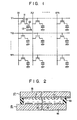
- Figs. 1 and 2 show an equivalent circuit of an active matrix type display apparatus having the TFT array and a schematic sectional view thereof.
- reference numeral 11 denotes a TFT as a switching element; and 12, a display pixel electrode which is connected to the source of the TFT 11 through a connecting portion 10.
- the connecting portion 10 is a small region which connects the source of the TFT 11 with the display pixel electrode 12 having a large area.
- the connecting portion 10 can be integrally formed with the display pixel electrode 12 and the source electrode of the TFT 11, or can be formed of a different conductive material. Gates of the TFTs 11 of each row are commonly connected to respective gate buses Y1, Y2,..., Yn.
- a first electrode substrate 15 comprises a transparent insulating substrate 16 formed of, e.g., glass on which the TFT array (not shown) and the display pixel electrode 12 driven thereby are formed.
- a second electrode substrate 17 comprises a transparent insulating substrate 18 formed of, e.g., glass on which the opposing electrode 13 formed of a transparent conductive film is formed.
- the liquid crystal layer 14 is sandwiched between these first and second electrode substrates 15 and 17.
- Reference numeral 19 denotes a spacer or sealing portion.
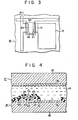
- FIG. 3 is a plan view showing a pattern of the first electrode substrate 15, and Fig. 4 is a detailed sectional view thereof.
- Japanese Patent Disclosure 56-27114 shows a pixel portion similar to that of Fig. 4.
- the first electrode substrate 15 can be obtained in the following manner.
- a drain electrode 20 formed of a transparent conductive film, the display pixel electrode 12 and a source electrode 21 integrally formed with the connecting portion 10 are formed on the transparent insulation substrate 16.
- a semiconductor thin film 22 is deposited on the thus obtained structure.
- a gate electrode 24 formed of, e.g., an AI film is formed on the semiconductorthin film 22 through a gate insulating film 23.
- a passivating film 25 formed of, e.g., an Si0 2 film is formed on the resultant structure, thus obtaining the first electrode substrate 15.
- the gate buses Y1, Y2,..., Yn are sequentially scanned and driven by a scanning signal.
- the TFTs 11 are sequentially turned on by each gate bus during a time period of T/n.
- Tf here means a frame scanning period.
- a TFT is easily subjected to light influence.
- a hydrogenated amorphous silicon film a-Si:H
- conductivity becomes more than thousand times of that upon irradiation with light.
- a leakage current is increased, thereby degrading performance of a transmission type display apparatus.
- a light shielding layer must be provided on the TFT portion.
- the signal voltage supplied through the TFT 11 and the connecting portion 10 is stored by a capacitor consisting of the display pixel electrode 12, the opposing electrode 13 and the liquid crystal layer 14.
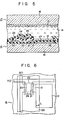
- a supplemental storage capacitor is connected in parallel to the capacitance of the liquid crystal layer 1 ' 4.
- a capacitor electrode 26 formed of a transparent conductive film is formed on the transparent insulating substrate 16, as shown in Fig. 5.
- a display apparatus similar to that shown in Fig. 5 is disclosed in Japanese Patent Disclosure 58-130561.
- an insulating film 27 formed of, e.g., an Si0 2 film is formed on the capacitor electrode 26.
- the TFT array and the display pixel electrode 12 are formed in the same manner as in Fig. 4.
- Prior art document US ⁇ A ⁇ 4. 239 346 describes a compact liquid crystal display system in which a metallic light blocking layer constitutes a part of a storage capacitor of a MOSFET. However, the system is a reflection type liquid crystal display device using a semiconductor backplate, and does not employ a liquid crystal display device of transmission type.
- the present invention provides an active matrix type display apparatus, comprising:
- an electrically conductive light shielding layer is provided on a TFT portion of a first electrode substrate and is set at a predetermined potential, and a part thereof opposes a part of a display pixel electrode through an insulating film so as to form an supplemental storage capacitor.
- the TFT portion is covered by the light shielding layer, and the supplemental storage capacitor is formed between the light shielding layer and the display pixel electrode, thereby obtaining a transmission type display apparatus having a good resistance to ambient light and a high signal-voltage storing property. Furthermore, according to the present invention, since the light shielding layer also serves as the supplemental storage capacitor electrode, the manufacturing process does not become complicated and the number of steps is not increased, and therefore a high manufacturing yield can be obtained.
- Figs. 6 and 7 show a structure of one pixel portion according to this embodiment of the present invention corresponding to Figs. 3 and 4, respectively. Therefore, the same reference numerals as in Figs. 3 and 4 denote the same parts in Figs. 6 and 7 and a detailed description thereof is omitted.
- the apparatus shown in Figs. 6 and 7 is different from the conventional apparatus in that an electrically conductive light shielding layer 28 is formed on a transparent insulating substrate 16 so as to cover a TFT region before forming a TFT 11, a display pixel electrode 12 and a connecting portion 10.
- This light shielding layer 28 comprises a metal film formed of, e.g., AI, Mo or Cr.
- a silicon nitride film 29 serving as an insulating film is formed on the light shielding layer 28, and the TFT 11 and the display pixel electrode 12 are formed thereon.
- each light shielding layer 28 is commonly provided along a column direction and is set at a predetermined potential such as a ground potential by an external circuit. This is because, if not, a drain electrode of the TFT 11 causes capacitive coupling with a source electrode 21 through the light shielding layer 28.
- the predetermined potential is not limited to the ground potential.
- the light shielding layer 28 opposes the entire surface of the display pixel electrode 12, transmission display cannot be performed.
- the light shielding layer 28 is formed to overlap a part of the display pixel electrode 12, and this overlapped portion forms the supplemental storage capacitor.
- the connecting portion 10 also forms a capacitor with the light shielding layer 28 and forms a portion of the supplemental storage capacitor.
- a capacitance C 1 of this supplemental storage capacitor can be determined by a permittivity and a thickness of the silicon nitride film 29 and an overlapped area of the light shielding layer 28, the display pixel electrode 12 and the connecting portion 10.
- a capacitance C 1 0.5 ⁇ 1 pF can easily be obtained by an overlapped area which is not so large as to practically affect light transmission at the display pixel portion.
- the capacitance C 1 was 0.85 pF.
- a capacitance formed in the overlapped portion of the connecting portion 10 and the light shielding layer 28 was in the order of 0.01 pF and contribution to the supplemental storage capacitor was extremely small.
- the display pixel electrode 12, the opposing electrode 13 and the liquid crystal layer 14 formed therebetween serve as a signal voltage storing capacitor.
- a pixel area S is 150 pmxl50 pm
- a dielectric constant e of a liquid crystal material is 8, and a thickness t of a cell is 8 pm
- a capacitance C 2 of this capacitor is about 0.2 pF.
- V o is the signal voltage initially stored in the display electrode.
- a display electrode potential drops to 1/3 or less of the initial potential V o , thereby undesirably decreasing an effective voltage applied to the liquid crystal layer and degrading the performance of the LCD.
- the manufacturing process does not become complicated and the number of steps is not increased, thereby improving a yield.
- Fig. 8 is a sectional view of one pixel portion according to another embodiment of the present invention corresponding to Fig. 7.
- a TFT 11 has a vertically inverted structure of that of the above embodiment.
- the same reference numerals as in Fig. 7 denote the same parts in Fig. 8.
- a gate electrode 24 of the TFT 11 is directly formed on a transparent insulating substrate 16. Since incidence of light from a side of a second elecgrode substrate 17 causes a problem, a light shielding layer 28 is formed on the TFT 11 and a display pixel electrode 12.
- the light shielding layer 28 overlaps with a part of the display pixel electrode 12 and a connecting portion 10 through a silicon nitride film 29, thereby constructing a supplemental storage capacitor in the same manner as in the above embodiment.
- the same effect as in the above embodiment can be obtained from this embodiment.
- a gate insulating film and an insulation film between a light shielding layer and a display pixel electrode are not limited to a silicon oxide film and silicon nitride film, but can be formed of an inorganic insulation film such as a silicon oxynitride film, or of an organic insulation film of, for example, polyimide.
- a light shielding layer can be formed of any conductive material which do not transmit light therethrough.
- this layer can be formed of a material having a relatively high resistance and can be a thin film of 100 nm to 200 nm.
- Each of the above-mentioned layers can be formed by plasma CVD, normal pressure or low pressure CVD, deposition, sputtering, molecular beam epitaxy, spin-on glass, or the like.
- a transparent electrode is directly formed as an opposing electrode on a transparent substrate in the above embodiments, the transparent electrode can be formed on a color filter formed on an insulating substrate, or the color filter can be provided after forming the transparent electrode.
- the present invention can be effectively applied to a display apparatus using an EL thin film instead of a liquid crystal material.
Claims (6)
Applications Claiming Priority (2)
| Application Number | Priority Date | Filing Date | Title |
|---|---|---|---|
| JP153771/83 | 1983-08-23 | ||
| JP58153771A JPS6045219A (ja) | 1983-08-23 | 1983-08-23 | アクテイブマトリクス型表示装置 |
Publications (3)
| Publication Number | Publication Date |
|---|---|
| EP0136509A2 EP0136509A2 (de) | 1985-04-10 |
| EP0136509A3 EP0136509A3 (en) | 1986-09-03 |
| EP0136509B1 true EP0136509B1 (de) | 1989-05-31 |
Family
ID=15569776
Family Applications (1)
| Application Number | Title | Priority Date | Filing Date |
|---|---|---|---|
| EP84109905A Expired EP0136509B1 (de) | 1983-08-23 | 1984-08-20 | Aktive Matrix-Anzeigevorrichtung |
Country Status (4)
| Country | Link |
|---|---|
| US (1) | US4759610A (de) |
| EP (1) | EP0136509B1 (de) |
| JP (1) | JPS6045219A (de) |
| DE (1) | DE3478514D1 (de) |
Families Citing this family (162)
| Publication number | Priority date | Publication date | Assignee | Title |
|---|---|---|---|---|
| JP3307150B2 (ja) * | 1995-03-20 | 2002-07-24 | ソニー株式会社 | アクティブマトリクス型表示装置 |
| US4904061A (en) * | 1984-10-22 | 1990-02-27 | Seiko Epson Corporation | Projection-type liquid crystal display device with even color |
| EP0198168A1 (de) * | 1985-02-21 | 1986-10-22 | OIS Optical Imaging Systems, Inc. | Aktive Matrix-Flüssigkristallanzeigen und Verfahren zu deren Herstellung |
| GB8508656D0 (en) * | 1985-04-03 | 1985-05-09 | Gen Electric Co Plc | Liquid crystal displays |
| DE3524085A1 (de) * | 1985-07-05 | 1987-01-08 | Vdo Schindling | Fluessigkristallzelle |
| JPS6280626A (ja) * | 1985-10-04 | 1987-04-14 | Hosiden Electronics Co Ltd | 液晶表示素子 |
| JPS6319876A (ja) * | 1986-07-11 | 1988-01-27 | Fuji Xerox Co Ltd | 薄膜トランジスタ装置 |
| JPH0691252B2 (ja) * | 1986-11-27 | 1994-11-14 | 日本電気株式会社 | 薄膜トランジスタアレイ |
| US5191450A (en) * | 1987-04-14 | 1993-03-02 | Seiko Epson Corporation | Projection-type color display device having a driving circuit for producing a mirror-like image |
| DE3852776T2 (de) * | 1987-04-14 | 1995-06-22 | Seiko Epson Corp | Projektions-Farbflüssigkristall-Anzeigevorrichtung. |
| JP2620240B2 (ja) * | 1987-06-10 | 1997-06-11 | 株式会社日立製作所 | 液晶表示装置 |
| US4810061A (en) * | 1987-06-24 | 1989-03-07 | Alps Electric Co., Ltd. | Liquid crystal element having conductive wiring part extending from top of transistor light shield to edge |
| US5198377A (en) * | 1987-07-31 | 1993-03-30 | Kinya Kato | Method of manufacturing an active matrix cell |
| US4918504A (en) * | 1987-07-31 | 1990-04-17 | Nippon Telegraph And Telephone Corporation | Active matrix cell |
| US4943839A (en) * | 1987-08-19 | 1990-07-24 | Ricoh Company, Ltd. | Contact type image sensor |
| US4839707A (en) * | 1987-08-27 | 1989-06-13 | Hughes Aircraft Company | LCMOS displays fabricated with implant treated silicon wafers |
| US5327001A (en) * | 1987-09-09 | 1994-07-05 | Casio Computer Co., Ltd. | Thin film transistor array having single light shield layer over transistors and gate and drain lines |
| US5229644A (en) * | 1987-09-09 | 1993-07-20 | Casio Computer Co., Ltd. | Thin film transistor having a transparent electrode and substrate |
| US4778258A (en) * | 1987-10-05 | 1988-10-18 | General Electric Company | Protective tab structure for use in the fabrication of matrix addressed thin film transistor liquid crystal displays |
| JPH01217325A (ja) * | 1988-02-25 | 1989-08-30 | Sharp Corp | 液晶表示装置 |
| US5231039A (en) * | 1988-02-25 | 1993-07-27 | Sharp Kabushiki Kaisha | Method of fabricating a liquid crystal display device |
| DE68917774T2 (de) * | 1988-04-30 | 1995-03-16 | Sharp Kk | Dünnfilm-Halbleitervorrichtung und damit hergestellte Flüssigkristallanzeige. |
| US5187551A (en) * | 1988-04-30 | 1993-02-16 | Sharp Kabushiki Kaisha | Thin film semiconductor device and liquid crystal display apparatus thereof for preventing irradiated light from reaching the semiconductor layers |
| JPH01302769A (ja) * | 1988-05-30 | 1989-12-06 | Seikosha Co Ltd | 逆スタガー型シリコン薄膜トランジスタの製造方法 |
| JPH0816756B2 (ja) * | 1988-08-10 | 1996-02-21 | シャープ株式会社 | 透過型アクティブマトリクス液晶表示装置 |
| US5042918A (en) * | 1988-11-15 | 1991-08-27 | Kabushiki Kaisha Toshiba | Liquid crystal display device |
| KR920008056B1 (ko) * | 1988-11-30 | 1992-09-22 | 주식회사 금성사 | 박막액정칼라티브이의 박막액티브매트릭스의 구조 |
| EP0376648B1 (de) * | 1988-12-26 | 1994-05-25 | Sharp Kabushiki Kaisha | Flüssigkristallanzeigevorrichtung |
| JP2600929B2 (ja) * | 1989-01-27 | 1997-04-16 | 松下電器産業株式会社 | 液晶画像表示装置およびその製造方法 |
| US4990460A (en) * | 1989-01-27 | 1991-02-05 | Nec Corporation | Fabrication method for thin film field effect transistor array suitable for liquid crystal display |
| US5270229A (en) * | 1989-03-07 | 1993-12-14 | Matsushita Electric Industrial Co., Ltd. | Thin film semiconductor device and process for producing thereof |
| JPH0734467B2 (ja) * | 1989-11-16 | 1995-04-12 | 富士ゼロックス株式会社 | イメージセンサ製造方法 |
| EP0438138B1 (de) * | 1990-01-17 | 1995-03-15 | Kabushiki Kaisha Toshiba | Flüssigkristall-Anzeigevorrichtung mit aktiver Matrix |
| JPH07112053B2 (ja) * | 1990-04-13 | 1995-11-29 | 富士ゼロックス株式会社 | 薄膜スイッチング素子アレイ |
| JPH0453929A (ja) * | 1990-06-22 | 1992-02-21 | Fujitsu Ltd | 反射型液晶装置 |
| GB2245741A (en) * | 1990-06-27 | 1992-01-08 | Philips Electronic Associated | Active matrix liquid crystal devices |
| JP3226223B2 (ja) * | 1990-07-12 | 2001-11-05 | 株式会社東芝 | 薄膜トランジスタアレイ装置および液晶表示装置 |
| JPH0824193B2 (ja) * | 1990-10-16 | 1996-03-06 | 工業技術院長 | 平板型光弁駆動用半導体装置の製造方法 |
| US5402254B1 (en) * | 1990-10-17 | 1998-09-22 | Hitachi Ltd | Liquid crystal display device with tfts in which pixel electrodes are formed in the same plane as the gate electrodes with anodized oxide films before the deposition of silicon |
| US5618739A (en) * | 1990-11-15 | 1997-04-08 | Seiko Instruments Inc. | Method of making light valve device using semiconductive composite substrate |
| US5347154A (en) * | 1990-11-15 | 1994-09-13 | Seiko Instruments Inc. | Light valve device using semiconductive composite substrate |
| US5177475A (en) * | 1990-12-19 | 1993-01-05 | Xerox Corporation | Control of liquid crystal devices |
| US5475514A (en) * | 1990-12-31 | 1995-12-12 | Kopin Corporation | Transferred single crystal arrayed devices including a light shield for projection displays |
| FR2679057B1 (fr) * | 1991-07-11 | 1995-10-20 | Morin Francois | Structure d'ecran a cristal liquide, a matrice active et a haute definition. |
| US6556257B2 (en) * | 1991-09-05 | 2003-04-29 | Sony Corporation | Liquid crystal display device |
| FR2682492B1 (fr) * | 1991-10-11 | 1993-12-03 | Thomson Lcd | Afficheur a matrice active utilisant un plan de masse enterre. |
| JP2900662B2 (ja) * | 1991-10-18 | 1999-06-02 | 三菱電機株式会社 | 薄膜トランジスタアレイ |
| JPH05249478A (ja) * | 1991-12-25 | 1993-09-28 | Toshiba Corp | 液晶表示装置 |
| JPH06194687A (ja) * | 1992-10-30 | 1994-07-15 | Nec Corp | 透過型アクティブマトリクス型液晶素子 |
| FR2687844A1 (fr) * | 1992-02-26 | 1993-08-27 | Chouan Yannick | Procede de fabrication d'un transistor en couches minces a double grille et a masque optique. |
| JP3205373B2 (ja) * | 1992-03-12 | 2001-09-04 | 株式会社日立製作所 | 液晶表示装置 |
| FR2689287B1 (fr) * | 1992-03-30 | 1997-01-03 | France Telecom | Ecran d'affichage a masque optique et procede de realisation de cet ecran. |
| JP2543286B2 (ja) * | 1992-04-22 | 1996-10-16 | インターナショナル・ビジネス・マシーンズ・コーポレイション | 液晶表示装置 |
| GB9211283D0 (en) * | 1992-05-28 | 1992-07-15 | Philips Electronics Uk Ltd | Liquid crystal display devices |
| JP3526058B2 (ja) * | 1992-08-19 | 2004-05-10 | セイコーインスツルメンツ株式会社 | 光弁用半導体装置 |
| US5633176A (en) * | 1992-08-19 | 1997-05-27 | Seiko Instruments Inc. | Method of producing a semiconductor device for a light valve |
| EP0592063A3 (en) * | 1992-09-14 | 1994-07-13 | Toshiba Kk | Active matrix liquid crystal display device |
| JPH0798460A (ja) | 1992-10-21 | 1995-04-11 | Seiko Instr Inc | 半導体装置及び光弁装置 |
| JP2924506B2 (ja) * | 1992-10-27 | 1999-07-26 | 日本電気株式会社 | アクティブマトリックス型液晶表示装置の画素構造 |
| KR960006205B1 (ko) * | 1992-12-30 | 1996-05-09 | 엘지전자주식회사 | 티에프티-엘씨디(tft-lcd)의 구조 |
| JP2812851B2 (ja) * | 1993-03-24 | 1998-10-22 | シャープ株式会社 | 反射型液晶表示装置 |
| JP2975844B2 (ja) * | 1993-06-24 | 1999-11-10 | 三洋電機株式会社 | 液晶表示装置 |
| KR0141774B1 (ko) * | 1994-06-17 | 1998-06-15 | 구자홍 | 액정표시장치 및 그 제조방법 |
| TW289097B (de) * | 1994-08-24 | 1996-10-21 | Hitachi Ltd | |
| JPH0887034A (ja) * | 1994-09-16 | 1996-04-02 | Toshiba Corp | 液晶表示装置およびその製造方法 |
| TW347477B (en) * | 1994-09-30 | 1998-12-11 | Sanyo Electric Co | Liquid crystal display with storage capacitors for holding electric charges |
| JP2770763B2 (ja) * | 1995-01-31 | 1998-07-02 | 日本電気株式会社 | アクティブマトリクス液晶表示装置 |
| FR2731526B1 (fr) * | 1995-03-09 | 1997-04-04 | Thomson Consumer Electronics | Ecran a cristaux liquides a angle de vue ameliore |
| JPH0926603A (ja) * | 1995-05-08 | 1997-01-28 | Semiconductor Energy Lab Co Ltd | 表示装置 |
| FR2734404B1 (fr) * | 1995-05-16 | 1997-06-27 | Thomson Lcd | Procede de fabrication de tft etages directs avec interconnexion grille-source ou drain |
| KR970011972A (ko) * | 1995-08-11 | 1997-03-29 | 쯔지 하루오 | 투과형 액정 표시 장치 및 그 제조 방법 |
| KR0171102B1 (ko) * | 1995-08-29 | 1999-03-20 | 구자홍 | 액정표시장치 구조 및 제조방법 |
| JP3184771B2 (ja) * | 1995-09-14 | 2001-07-09 | キヤノン株式会社 | アクティブマトリックス液晶表示装置 |
| JPH0990397A (ja) * | 1995-09-28 | 1997-04-04 | Sharp Corp | アクティブマトリクス基板およびそれを用いた表示装置 |
| JP3272212B2 (ja) * | 1995-09-29 | 2002-04-08 | シャープ株式会社 | 透過型液晶表示装置およびその製造方法 |
| US6800875B1 (en) * | 1995-11-17 | 2004-10-05 | Semiconductor Energy Laboratory Co., Ltd. | Active matrix electro-luminescent display device with an organic leveling layer |
| TWI228625B (en) * | 1995-11-17 | 2005-03-01 | Semiconductor Energy Lab | Display device |
| JPH09146108A (ja) * | 1995-11-17 | 1997-06-06 | Semiconductor Energy Lab Co Ltd | 液晶表示装置およびその駆動方法 |
| JP2720862B2 (ja) * | 1995-12-08 | 1998-03-04 | 日本電気株式会社 | 薄膜トランジスタおよび薄膜トランジスタアレイ |
| TW309633B (de) * | 1995-12-14 | 1997-07-01 | Handotai Energy Kenkyusho Kk | |
| US6682961B1 (en) | 1995-12-29 | 2004-01-27 | Samsung Electronics Co., Ltd. | Thin film transistor array panel used for a liquid crystal display and a manufacturing method thereof |
| US5782665A (en) * | 1995-12-29 | 1998-07-21 | Xerox Corporation | Fabricating array with storage capacitor between cell electrode and dark matrix |
| JP3729955B2 (ja) * | 1996-01-19 | 2005-12-21 | 株式会社半導体エネルギー研究所 | 半導体装置の作製方法 |
| JP3645378B2 (ja) | 1996-01-19 | 2005-05-11 | 株式会社半導体エネルギー研究所 | 半導体装置の作製方法 |
| US6478263B1 (en) | 1997-01-17 | 2002-11-12 | Semiconductor Energy Laboratory Co., Ltd. | Semiconductor device and its manufacturing method |
| JP3645380B2 (ja) | 1996-01-19 | 2005-05-11 | 株式会社半導体エネルギー研究所 | 半導体装置の作製方法、情報端末、ヘッドマウントディスプレイ、ナビゲーションシステム、携帯電話、ビデオカメラ、投射型表示装置 |
| JP3645379B2 (ja) | 1996-01-19 | 2005-05-11 | 株式会社半導体エネルギー研究所 | 半導体装置の作製方法 |
| US6180439B1 (en) * | 1996-01-26 | 2001-01-30 | Semiconductor Energy Laboratory Co., Ltd. | Method for fabricating a semiconductor device |
| US7056381B1 (en) | 1996-01-26 | 2006-06-06 | Semiconductor Energy Laboratory Co., Ltd. | Fabrication method of semiconductor device |
| JP3647542B2 (ja) * | 1996-02-20 | 2005-05-11 | 株式会社半導体エネルギー研究所 | 液晶表示装置 |
| JP3205501B2 (ja) * | 1996-03-12 | 2001-09-04 | シャープ株式会社 | アクティブマトリクス表示装置およびその修正方法 |
| US6100562A (en) | 1996-03-17 | 2000-08-08 | Semiconductor Energy Laboratory Co., Ltd. | Method of manufacturing a semiconductor device |
| JP2734444B2 (ja) * | 1996-03-22 | 1998-03-30 | 日本電気株式会社 | 液晶表示装置 |
| JP3468986B2 (ja) * | 1996-04-16 | 2003-11-25 | 株式会社半導体エネルギー研究所 | アクティブマトリクス回路および表示装置 |
| JP3685869B2 (ja) | 1996-05-08 | 2005-08-24 | 株式会社半導体エネルギー研究所 | 液晶表示装置 |
| US6005648A (en) * | 1996-06-25 | 1999-12-21 | Semiconductor Energy Laboratory Co., Ltd. | Display device |
| JP3126661B2 (ja) * | 1996-06-25 | 2001-01-22 | 株式会社半導体エネルギー研究所 | 液晶表示装置 |
| JPH1020298A (ja) * | 1996-07-03 | 1998-01-23 | Sharp Corp | 液晶表示装置 |
| JP3708637B2 (ja) * | 1996-07-15 | 2005-10-19 | 株式会社半導体エネルギー研究所 | 液晶表示装置 |
| JP3634089B2 (ja) * | 1996-09-04 | 2005-03-30 | 株式会社半導体エネルギー研究所 | 表示装置 |
| TWI236556B (en) | 1996-10-16 | 2005-07-21 | Seiko Epson Corp | Substrate for a liquid crystal equipment, liquid crystal equipment and projection type display equipment |
| US7872728B1 (en) | 1996-10-22 | 2011-01-18 | Seiko Epson Corporation | Liquid crystal panel substrate, liquid crystal panel, and electronic device and projection display device using the same |
| US6831623B2 (en) * | 1996-10-22 | 2004-12-14 | Seiko Epson Corporation | Liquid crystal panel substrate, liquid crystal panel, and electronic equipment and projection type display device both using the same |
| JP3716580B2 (ja) | 1997-02-27 | 2005-11-16 | セイコーエプソン株式会社 | 液晶装置及びその製造方法、並びに投写型表示装置 |
| JP3784491B2 (ja) * | 1997-03-28 | 2006-06-14 | 株式会社半導体エネルギー研究所 | アクティブマトリクス型の表示装置 |
| TW508470B (en) * | 1997-05-09 | 2002-11-01 | Hitachi Ltd | Liquid crystal display device |
| JP4396599B2 (ja) * | 1997-10-31 | 2010-01-13 | セイコーエプソン株式会社 | 液晶装置及び電子機器並びに投射型表示装置 |
| JPH11202349A (ja) * | 1998-01-12 | 1999-07-30 | Semiconductor Energy Lab Co Ltd | 表示装置 |
| CN101533192B (zh) * | 1998-02-09 | 2011-08-03 | 精工爱普生株式会社 | 液晶板及电子设备 |
| GB9803764D0 (en) * | 1998-02-23 | 1998-04-15 | Cambridge Display Tech Ltd | Display devices |
| JP4312851B2 (ja) | 1998-04-27 | 2009-08-12 | 株式会社半導体エネルギー研究所 | 半導体装置およびその作製方法 |
| JP3941901B2 (ja) * | 1998-04-28 | 2007-07-11 | 株式会社半導体エネルギー研究所 | 半導体装置の作製方法 |
| GB9811477D0 (en) * | 1998-05-29 | 1998-07-29 | Sharp Kk | Liquid crystal device |
| KR100333179B1 (ko) | 1998-06-30 | 2002-08-24 | 주식회사 현대 디스플레이 테크놀로지 | 박막트랜지스터액정표시소자및그의제조방법 |
| US6313481B1 (en) | 1998-08-06 | 2001-11-06 | Semiconductor Energy Laboratory Co., Ltd. | Semiconductor device and a method of manufacturing the same |
| JP3141860B2 (ja) * | 1998-10-28 | 2001-03-07 | ソニー株式会社 | 液晶表示装置の製造方法 |
| US6475836B1 (en) | 1999-03-29 | 2002-11-05 | Semiconductor Energy Laboratory Co., Ltd. | Semiconductor device and manufacturing method thereof |
| US7288420B1 (en) * | 1999-06-04 | 2007-10-30 | Semiconductor Energy Laboratory Co., Ltd. | Method for manufacturing an electro-optical device |
| JP2001109404A (ja) * | 1999-10-01 | 2001-04-20 | Sanyo Electric Co Ltd | El表示装置 |
| GB9928353D0 (en) * | 1999-12-01 | 2000-01-26 | Koninkl Philips Electronics Nv | Liquid crystal display and method of manufacture |
| US6590227B2 (en) * | 1999-12-27 | 2003-07-08 | Semiconductor Energy Laboratory Co., Ltd. | Active matrix display device |
| TW521303B (en) * | 2000-02-28 | 2003-02-21 | Semiconductor Energy Lab | Electronic device |
| GB0014962D0 (en) * | 2000-06-20 | 2000-08-09 | Koninkl Philips Electronics Nv | Matrix array display devices with light sensing elements and associated storage capacitors |
| US20020097350A1 (en) * | 2000-09-19 | 2002-07-25 | Haven Duane A. | Thin film transistors suitable for use in flat panel displays |
| DE10057696A1 (de) * | 2000-11-21 | 2002-05-16 | Siemens Ag | LC-Display und Verfahren zum Steuern der Hinterleuchtung eines LC-Displays |
| US6897477B2 (en) * | 2001-06-01 | 2005-05-24 | Semiconductor Energy Laboratory Co., Ltd. | Semiconductor device, manufacturing method thereof, and display device |
| AU2002336341A1 (en) * | 2002-02-20 | 2003-09-09 | Planar Systems, Inc. | Light sensitive display |
| US7009663B2 (en) | 2003-12-17 | 2006-03-07 | Planar Systems, Inc. | Integrated optical light sensitive active matrix liquid crystal display |
| US7053967B2 (en) | 2002-05-23 | 2006-05-30 | Planar Systems, Inc. | Light sensitive display |
| US7023503B2 (en) * | 2002-02-20 | 2006-04-04 | Planar Systems, Inc. | Image sensor with photosensitive thin film transistors |
| US7372510B2 (en) * | 2002-03-01 | 2008-05-13 | Planar Systems, Inc. | Reflection resistant touch screens |
| JP4551049B2 (ja) * | 2002-03-19 | 2010-09-22 | 三菱電機株式会社 | 表示装置 |
| US20060034492A1 (en) * | 2002-10-30 | 2006-02-16 | Roy Siegel | Hand recognition system |
| US20080084374A1 (en) | 2003-02-20 | 2008-04-10 | Planar Systems, Inc. | Light sensitive display |
| US20050134749A1 (en) * | 2003-12-19 | 2005-06-23 | Adiel Abileah | Reflection resistant display |
| JP2007532978A (ja) * | 2004-04-13 | 2007-11-15 | ジ・アリゾナ・ボード・オブ・リージェンツ・オン・ビハーフ・オブ・ザ・ユニバーシティー・オブ・アリゾナ | 電気的に活性の液晶眼科用装置のパターン化された電極 |
| US7773139B2 (en) | 2004-04-16 | 2010-08-10 | Apple Inc. | Image sensor with photosensitive thin film transistors |
| KR101017157B1 (ko) * | 2004-06-30 | 2011-02-25 | 엘지디스플레이 주식회사 | 액정 표시 장치용 어레이 기판 및 그 제조 방법 |
| US8350466B2 (en) | 2004-09-17 | 2013-01-08 | Semiconductor Energy Laboratory Co., Ltd. | Display device and manufacturing method thereof |
| US7753751B2 (en) | 2004-09-29 | 2010-07-13 | Semiconductor Energy Laboratory Co., Ltd. | Method of fabricating the display device |
| US8772783B2 (en) * | 2004-10-14 | 2014-07-08 | Semiconductor Energy Laboratory Co., Ltd. | Display device |
| US7525194B2 (en) * | 2005-07-27 | 2009-04-28 | Palo Alto Research Center Incorporated | System including self-assembled interconnections |
| US7504331B2 (en) * | 2005-07-27 | 2009-03-17 | Palo Alto Research Center Incorporated | Method of fabricating self-assembled electrical interconnections |
| US7662708B2 (en) * | 2005-07-27 | 2010-02-16 | Palo Alto Research Center Incorporated | Self-assembled interconnection particles |
| KR101230307B1 (ko) | 2006-02-17 | 2013-02-06 | 삼성디스플레이 주식회사 | 액정 표시 장치 |
| TWI387822B (zh) * | 2008-07-01 | 2013-03-01 | Chunghwa Picture Tubes Ltd | 薄膜電晶體陣列基板及其製造方法 |
| TWI607670B (zh) * | 2009-01-08 | 2017-12-01 | 半導體能源研究所股份有限公司 | 發光裝置及電子裝置 |
| JP5630169B2 (ja) * | 2010-09-14 | 2014-11-26 | カシオ計算機株式会社 | トランジスタ構造体の製造方法 |
| JP5630170B2 (ja) * | 2010-09-14 | 2014-11-26 | カシオ計算機株式会社 | トランジスタ構造体の製造方法 |
| US9310923B2 (en) | 2010-12-03 | 2016-04-12 | Apple Inc. | Input device for touch sensitive devices |
| US8928635B2 (en) | 2011-06-22 | 2015-01-06 | Apple Inc. | Active stylus |
| US9329703B2 (en) | 2011-06-22 | 2016-05-03 | Apple Inc. | Intelligent stylus |
| US8638320B2 (en) | 2011-06-22 | 2014-01-28 | Apple Inc. | Stylus orientation detection |
| TWI451179B (zh) | 2011-11-17 | 2014-09-01 | Au Optronics Corp | 畫素結構及其製造方法 |
| KR101945237B1 (ko) * | 2012-06-01 | 2019-02-08 | 삼성디스플레이 주식회사 | 유기 발광 표시 장치 |
| US9557845B2 (en) | 2012-07-27 | 2017-01-31 | Apple Inc. | Input device for and method of communication with capacitive devices through frequency variation |
| US9176604B2 (en) | 2012-07-27 | 2015-11-03 | Apple Inc. | Stylus device |
| US9652090B2 (en) | 2012-07-27 | 2017-05-16 | Apple Inc. | Device for digital communication through capacitive coupling |
| US10048775B2 (en) | 2013-03-14 | 2018-08-14 | Apple Inc. | Stylus detection and demodulation |
| US10845901B2 (en) | 2013-07-31 | 2020-11-24 | Apple Inc. | Touch controller architecture |
| US10061450B2 (en) | 2014-12-04 | 2018-08-28 | Apple Inc. | Coarse scan and targeted active mode scan for touch |
| US10474277B2 (en) | 2016-05-31 | 2019-11-12 | Apple Inc. | Position-based stylus communication |
Family Cites Families (13)
| Publication number | Priority date | Publication date | Assignee | Title |
|---|---|---|---|---|
| US3840695A (en) * | 1972-10-10 | 1974-10-08 | Westinghouse Electric Corp | Liquid crystal image display panel with integrated addressing circuitry |
| US3824003A (en) * | 1973-05-07 | 1974-07-16 | Hughes Aircraft Co | Liquid crystal display panel |
| US4040073A (en) * | 1975-08-29 | 1977-08-02 | Westinghouse Electric Corporation | Thin film transistor and display panel using the transistor |
| JPS5854393B2 (ja) * | 1976-08-31 | 1983-12-05 | シャープ株式会社 | 液晶表示装置 |
| JPS5499576A (en) * | 1978-01-23 | 1979-08-06 | Sharp Corp | Thin-film transistor and its manufacture |
| US4196973A (en) * | 1978-08-21 | 1980-04-08 | Timex Corporation | Transflector for illuminated electrooptic displays |
| US4239346A (en) * | 1979-05-23 | 1980-12-16 | Hughes Aircraft Company | Compact liquid crystal display system |
| US4431271A (en) * | 1979-09-06 | 1984-02-14 | Canon Kabushiki Kaisha | Display device with a thin film transistor and storage condenser |
| JPS56107287A (en) * | 1980-01-31 | 1981-08-26 | Tokyo Shibaura Electric Co | Image display unit |
| DE3153620C2 (de) * | 1980-04-01 | 1992-01-23 | Canon K.K., Tokio/Tokyo, Jp | |
| JPS58159516A (ja) * | 1982-03-18 | 1983-09-21 | Seiko Epson Corp | 液晶表示パネル |
| JPS595229A (ja) * | 1982-07-01 | 1984-01-12 | Asahi Glass Co Ltd | 画像表示装置 |
| US4545112A (en) * | 1983-08-15 | 1985-10-08 | Alphasil Incorporated | Method of manufacturing thin film transistors and transistors made thereby |
-
1983
- 1983-08-23 JP JP58153771A patent/JPS6045219A/ja active Pending
-
1984
- 1984-08-20 DE DE8484109905T patent/DE3478514D1/de not_active Expired
- 1984-08-20 EP EP84109905A patent/EP0136509B1/de not_active Expired
-
1986
- 1986-09-29 US US06/913,560 patent/US4759610A/en not_active Expired - Lifetime
Also Published As
| Publication number | Publication date |
|---|---|
| JPS6045219A (ja) | 1985-03-11 |
| EP0136509A3 (en) | 1986-09-03 |
| US4759610A (en) | 1988-07-26 |
| DE3478514D1 (en) | 1989-07-06 |
| EP0136509A2 (de) | 1985-04-10 |
Similar Documents
| Publication | Publication Date | Title |
|---|---|---|
| EP0136509B1 (de) | Aktive Matrix-Anzeigevorrichtung | |
| US5028122A (en) | Liquid crystal active-matrix display device | |
| JP4483235B2 (ja) | トランジスタアレイ基板の製造方法及びトランジスタアレイ基板 | |
| US6855954B1 (en) | Thin film transistor, fabrication method thereof and liquid crystal display having the thin film transistor | |
| EP0376437B1 (de) | Flüssigkristallanzeige mit aktiver Matrix | |
| US5062690A (en) | Liquid crystal display with redundant FETS and redundant crossovers connected by laser-fusible links | |
| US6376270B1 (en) | Method of making an array of TFTs having an insulation layer with a low dielectric constant | |
| TW446832B (en) | Liquid crystal display device | |
| EP0372821B1 (de) | Flüssigkristallanzeigetafel mit verminderten Pixeldefekten | |
| EP0661581B1 (de) | Flüssigkristall-Anzeigevorrichtung mit aktiver Matrix | |
| US4938567A (en) | Electro-optical display panel with control transistors and method for making it | |
| US6222595B1 (en) | TFT-LCD having pixel electrode overlapping scan and data lines except at the intersection of lines | |
| JPH1031235A (ja) | 液晶表示装置 | |
| US5231039A (en) | Method of fabricating a liquid crystal display device | |
| GB2329061A (en) | Liquid crystal display and method of manufacturing the same. | |
| JP2000227611A (ja) | 液晶表示装置とその製造方法 | |
| US20010045995A1 (en) | Liquid crystal display and manufacturing method therfor | |
| JP2003344866A5 (de) | ||
| US7705925B2 (en) | Method of manufacturing an array substrate for use in a LCD device | |
| US7936424B2 (en) | Liquid crystal display panel with light leakage prevention film and method for manufacturing the same | |
| JP2584290B2 (ja) | 液晶表示装置の製造方法 | |
| US5432625A (en) | Display screen having opaque conductive optical mask and TFT of semiconductive, insulating, and conductive layers on first transparent conductive film | |
| US6278502B1 (en) | Pixel capacitor formed from multiple layers | |
| JP2639980B2 (ja) | 液晶表示装置 | |
| JP3405988B2 (ja) | 埋込み接地面を利用する活性マトリックス表示装置 |
Legal Events
| Date | Code | Title | Description |
|---|---|---|---|
| PUAI | Public reference made under article 153(3) epc to a published international application that has entered the european phase |
Free format text: ORIGINAL CODE: 0009012 |
|
| 17P | Request for examination filed |
Effective date: 19840917 |
|
| AK | Designated contracting states |
Designated state(s): DE FR GB |
|
| PUAL | Search report despatched |
Free format text: ORIGINAL CODE: 0009013 |
|
| AK | Designated contracting states |
Kind code of ref document: A3 Designated state(s): DE FR GB |
|
| 17Q | First examination report despatched |
Effective date: 19880308 |
|
| GRAA | (expected) grant |
Free format text: ORIGINAL CODE: 0009210 |
|
| AK | Designated contracting states |
Kind code of ref document: B1 Designated state(s): DE FR GB |
|
| REF | Corresponds to: |
Ref document number: 3478514 Country of ref document: DE Date of ref document: 19890706 |
|
| ET | Fr: translation filed | ||
| PLBE | No opposition filed within time limit |
Free format text: ORIGINAL CODE: 0009261 |
|
| STAA | Information on the status of an ep patent application or granted ep patent |
Free format text: STATUS: NO OPPOSITION FILED WITHIN TIME LIMIT |
|
| 26N | No opposition filed | ||
| REG | Reference to a national code |
Ref country code: GB Ref legal event code: 746 Effective date: 19981026 |
|
| REG | Reference to a national code |
Ref country code: FR Ref legal event code: D6 |
|
| REG | Reference to a national code |
Ref country code: GB Ref legal event code: IF02 |
|
| PGFP | Annual fee paid to national office [announced via postgrant information from national office to epo] |
Ref country code: FR Payment date: 20030808 Year of fee payment: 20 |
|
| PGFP | Annual fee paid to national office [announced via postgrant information from national office to epo] |
Ref country code: GB Payment date: 20030820 Year of fee payment: 20 |
|
| PGFP | Annual fee paid to national office [announced via postgrant information from national office to epo] |
Ref country code: DE Payment date: 20030828 Year of fee payment: 20 |
|
| PG25 | Lapsed in a contracting state [announced via postgrant information from national office to epo] |
Ref country code: GB Free format text: LAPSE BECAUSE OF EXPIRATION OF PROTECTION Effective date: 20040819 |
|
| REG | Reference to a national code |
Ref country code: GB Ref legal event code: PE20 |