WO2021049033A1 - メモリシステム - Google Patents
メモリシステム Download PDFInfo
- Publication number
- WO2021049033A1 WO2021049033A1 PCT/JP2019/036211 JP2019036211W WO2021049033A1 WO 2021049033 A1 WO2021049033 A1 WO 2021049033A1 JP 2019036211 W JP2019036211 W JP 2019036211W WO 2021049033 A1 WO2021049033 A1 WO 2021049033A1
- Authority
- WO
- WIPO (PCT)
- Prior art keywords
- data
- signal
- output
- memory
- controller
- Prior art date
- Legal status (The legal status is an assumption and is not a legal conclusion. Google has not performed a legal analysis and makes no representation as to the accuracy of the status listed.)
- Ceased
Links
Images







Classifications
-
- G—PHYSICS
- G06—COMPUTING OR CALCULATING; COUNTING
- G06F—ELECTRIC DIGITAL DATA PROCESSING
- G06F3/00—Input arrangements for transferring data to be processed into a form capable of being handled by the computer; Output arrangements for transferring data from processing unit to output unit, e.g. interface arrangements
- G06F3/06—Digital input from, or digital output to, record carriers, e.g. RAID, emulated record carriers or networked record carriers
- G06F3/0601—Interfaces specially adapted for storage systems
- G06F3/0628—Interfaces specially adapted for storage systems making use of a particular technique
- G06F3/0655—Vertical data movement, i.e. input-output transfer; data movement between one or more hosts and one or more storage devices
-
- G—PHYSICS
- G06—COMPUTING OR CALCULATING; COUNTING
- G06F—ELECTRIC DIGITAL DATA PROCESSING
- G06F12/00—Accessing, addressing or allocating within memory systems or architectures
- G06F12/02—Addressing or allocation; Relocation
- G06F12/0223—User address space allocation, e.g. contiguous or non contiguous base addressing
- G06F12/023—Free address space management
- G06F12/0238—Memory management in non-volatile memory, e.g. resistive RAM or ferroelectric memory
- G06F12/0246—Memory management in non-volatile memory, e.g. resistive RAM or ferroelectric memory in block erasable memory, e.g. flash memory
-
- G—PHYSICS
- G11—INFORMATION STORAGE
- G11C—STATIC STORES
- G11C16/00—Erasable programmable read-only memories
- G11C16/02—Erasable programmable read-only memories electrically programmable
- G11C16/06—Auxiliary circuits, e.g. for writing into memory
- G11C16/26—Sensing or reading circuits; Data output circuits
-
- G—PHYSICS
- G06—COMPUTING OR CALCULATING; COUNTING
- G06F—ELECTRIC DIGITAL DATA PROCESSING
- G06F13/00—Interconnection of, or transfer of information or other signals between, memories, input/output devices or central processing units
- G06F13/14—Handling requests for interconnection or transfer
- G06F13/16—Handling requests for interconnection or transfer for access to memory bus
- G06F13/1668—Details of memory controller
-
- G—PHYSICS
- G06—COMPUTING OR CALCULATING; COUNTING
- G06F—ELECTRIC DIGITAL DATA PROCESSING
- G06F3/00—Input arrangements for transferring data to be processed into a form capable of being handled by the computer; Output arrangements for transferring data from processing unit to output unit, e.g. interface arrangements
- G06F3/06—Digital input from, or digital output to, record carriers, e.g. RAID, emulated record carriers or networked record carriers
- G06F3/0601—Interfaces specially adapted for storage systems
- G06F3/0602—Interfaces specially adapted for storage systems specifically adapted to achieve a particular effect
- G06F3/0604—Improving or facilitating administration, e.g. storage management
-
- G—PHYSICS
- G06—COMPUTING OR CALCULATING; COUNTING
- G06F—ELECTRIC DIGITAL DATA PROCESSING
- G06F3/00—Input arrangements for transferring data to be processed into a form capable of being handled by the computer; Output arrangements for transferring data from processing unit to output unit, e.g. interface arrangements
- G06F3/06—Digital input from, or digital output to, record carriers, e.g. RAID, emulated record carriers or networked record carriers
- G06F3/0601—Interfaces specially adapted for storage systems
- G06F3/0668—Interfaces specially adapted for storage systems adopting a particular infrastructure
- G06F3/0671—In-line storage system
- G06F3/0673—Single storage device
- G06F3/0679—Non-volatile semiconductor memory device, e.g. flash memory, one time programmable memory [OTP]
-
- G—PHYSICS
- G11—INFORMATION STORAGE
- G11C—STATIC STORES
- G11C16/00—Erasable programmable read-only memories
- G11C16/02—Erasable programmable read-only memories electrically programmable
- G11C16/04—Erasable programmable read-only memories electrically programmable using variable threshold transistors, e.g. FAMOS
- G11C16/0483—Erasable programmable read-only memories electrically programmable using variable threshold transistors, e.g. FAMOS comprising cells having several storage transistors connected in series
-
- G—PHYSICS
- G11—INFORMATION STORAGE
- G11C—STATIC STORES
- G11C7/00—Arrangements for writing information into, or reading information out from, a digital store
- G11C7/10—Input/output [I/O] data interface arrangements, e.g. I/O data control circuits, I/O data buffers
- G11C7/1051—Data output circuits, e.g. read-out amplifiers, data output buffers, data output registers, data output level conversion circuits
- G11C7/1063—Control signal output circuits, e.g. status or busy flags, feedback command signals
-
- G—PHYSICS
- G11—INFORMATION STORAGE
- G11C—STATIC STORES
- G11C7/00—Arrangements for writing information into, or reading information out from, a digital store
- G11C7/22—Read-write [R-W] timing or clocking circuits; Read-write [R-W] control signal generators or management
-
- G—PHYSICS
- G06—COMPUTING OR CALCULATING; COUNTING
- G06F—ELECTRIC DIGITAL DATA PROCESSING
- G06F2212/00—Indexing scheme relating to accessing, addressing or allocation within memory systems or architectures
- G06F2212/72—Details relating to flash memory management
- G06F2212/7201—Logical to physical mapping or translation of blocks or pages
Definitions
- the embodiment relates to a memory system.
- NAND flash memory as a semiconductor storage device is known.
- the memory system of the embodiment includes a semiconductor memory and a controller that gives an instruction to read data from the semiconductor memory, and the semiconductor memory is read from a memory cell transistor that holds data and the memory cell transistor.
- the controller includes an output circuit that performs processing for outputting the data to the controller and a data generation circuit that generates the first data.
- the output circuit of the controller is the same.
- the first signal is output to the semiconductor memory within the first period during the processing, and the semiconductor memory generates a second signal based on the first signal during the first period and the second period.
- the first data is output to the controller together with the second signal, and after the end of the second period, the semiconductor memory outputs the data read from the memory cell transistor together with the second signal to the controller. ..
- FIG. 1 is a block diagram conceptually showing the overall configuration of the memory system according to the embodiment.
- FIG. 2 is a block diagram showing a configuration example of a NAND flash memory.
- FIG. 3 is a circuit diagram showing a configuration example of a memory cell array of a NAND flash memory.
- FIG. 4 is a block diagram showing a configuration example of the output circuit.
- FIG. 5 is a flowchart of an example to be compared with the embodiment.
- FIG. 6A is a timing chart for explaining a data output operation according to an example to be compared with the embodiment.
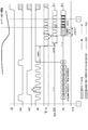
- FIG. 6B is a timing chart for explaining the stabilization of the power supply output in the data output operation according to the first embodiment.
- FIG. 7 is a flowchart for explaining stabilization of the power supply output in the data output operation according to the first embodiment.
- FIG. 8 is a timing chart showing the timing of each signal in the standby time and the delay time according to the first setting example.
- FIG. 9 is a timing chart showing the timing of each signal in the standby time and the delay time according to the second setting example.
- FIG. 10 is a timing chart showing the timing of each signal in the standby time and the delay time according to the third setting example.
- FIG. 11 is a timing chart showing the timing of each signal in the standby time and the delay time according to the fourth setting example.
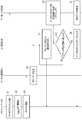
- FIG. 12 is a flowchart for explaining stabilization of the power supply output in the data output operation according to the second embodiment.
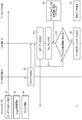
- FIG. 13 is a flowchart for explaining stabilization of the power supply output in the data output operation according to the third embodiment.
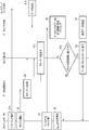
- FIG. 14 is a flowchart for explaining stabilization of the power supply output in the data output operation according to the fourth embodiment.
- FIG. 15 is a timing chart showing the timing of each signal in the electric standby time and the delay time according to the fifth embodiment.
- FIG. 1 is a configuration diagram conceptually showing the overall configuration of the memory system 1 of the present embodiment.
- the memory system 1 of the present embodiment includes at least a semiconductor memory 3 and a memory controller (controller) 2 that controls the semiconductor memory 3.
- the semiconductor memory 3 may be a non-volatile memory, and for example, a NAND flash memory is suitable.
- NAND flash memory is suitable.
- memory controllers 2 and the NAND flash memory 3 it is possible to combine these memory controllers 2 and the NAND flash memory 3 to form one semiconductor device. Examples thereof include memory cards such as SD TM cards and SSDs (solid state drives). Further, the memory controller 2 can use a SoC (system on chip) or the like.
- SoC system on chip
- the NAND flash memory 3 includes a plurality of memory cell transistors and stores data non-volatilely.
- the memory controller 2 is connected to the NAND flash memory 3 by the NAND bus. Further, the memory controller 2 is also connected to the external host device 4 by the host bus.
- the memory controller 2 controls the NAND flash memory 3 and accesses the NAND flash memory 3 in response to an instruction received from the host device 4.
- the host device 4 is, for example, a digital camera, a personal computer, or the like, and the host bus is, for example, a bus that follows an SDTM interface.
- the NAND bus sends and receives signals according to the NAND interface.
- the memory controller 2 controls the NAND flash memory 3. As a specific example, the memory controller 2 controls to write data to the NAND flash memory 3 and read the already stored data from the NAND flash memory 3.
- the memory controller 2 includes a host interface circuit (host I / F) 5, a built-in memory (RAM: Random Access Memory) 6, a processor (CPU: Central Processing Unit) 7, a buffer memory 8, and a NAND interface circuit (NAND I / F) 9. , And an ECC (Error Checking and Correcting) circuit 10. Further, various other constituent parts are mounted depending on the design.
- host I / F host interface circuit
- RAM Random Access Memory
- processor CPU: Central Processing Unit
- NAND I / F NAND interface circuit
- ECC Error Checking and Correcting
- the host interface circuit 5 is connected to the host device 4 via the host bus, and transfers the instructions and data received from the host device 4 to the processor 7 and the buffer memory 8, respectively. Further, the data in the buffer memory 8 is transferred to the host device 4 in response to the instruction of the processor 7.
- the processor 7 controls the operation of the entire memory controller 2. For example, when the processor 7 receives a data write instruction from the host device 4, the processor 7 issues a write instruction to the NAND interface circuit 9 in response to the reception. The same applies when reading and erasing data. Further, the processor 7 executes various processes for managing the NAND flash memory 3, such as wear leveling.
- the operation of the memory controller 2 described below may be realized by the processor 7 executing software (firmware), or may be realized by hardware.
- the NAND interface circuit 9 is connected to the NAND flash memory 3 via the NAND bus and controls communication with the NAND flash memory 3. Then, the NAND interface circuit 9 transmits and receives various signals to the NAND flash memory 3 based on the instruction received from the processor 7.
- the buffer memory 8 temporarily holds write data and read data.
- the built-in memory (RAM) 6 is, for example, a semiconductor memory such as a DRAM or SRAM, and is used as a work area of the processor 7.
- the built-in memory 6 holds firmware for managing the NAND flash memory 3, various management tables, and the like.
- the ECC circuit 10 performs error detection and error correction processing on the data stored in the NAND flash memory 3. That is, the ECC circuit 10 generates an error correction code when writing data, assigns it to the written data, and decodes the error correction code when reading the data.
- the NAND bus will be described with reference to FIG.
- the memory controller 2 and the NAND flash memory 3 are connected by a NAND bus.
- the NAND bus includes a plurality of signal lines, and includes a signal line group connected to the input / output pad group 21 connected to the input / output circuit 12 and a signal line connected to the logic control pad group 22 connected to the logic control circuit 13. Divided into groups.
- These signal lines include chip enable signal / CE, command latch enable signal CLE, address latch enable signal ALE, write enable signal / WE, read enable signal / RE, write protect signal / WP, and ready signal according to the NAND interface.
- the busy signal / RB, the data signal DQ, the data strobe signal DQS, and / DQS are transmitted and received.
- the signals CLE, ALE, / WE, / RE, and / WP are received by the NAND flash memory 3. Further, the signal / RB and the signal / CE are each received by the NAND flash memory 3.
- the chip enable signal / CE is a signal for enabling the NAND flash memory 3.
- the command latch enable signal CLE makes it possible to latch the command CMD transmitted as the data signal DQ to the command register 15A of the register 15 described later.
- the signal CLE notifies the NAND flash memory 3 that the signal DQ flowing through the NAND flash memory 3 is the command CMD while the signal CLE is at the “H (High)” level.
- the signal DQ is, for example, an 8-bit signal.
- the address latch enable signal ALE makes it possible to latch the address ADD transmitted as the data signal DQ to the address register 15B of the register 15 described later.
- the signal ALE notifies the NAND flash memory 3 that the signal DQ transmitted to the NAND flash memory 3 is the address ADD while the signal ALE is at the “H” level.
- the write enable signal / WE enables writing.
- the signal / WE instructs the NAND flash memory 3 to capture the signal DQ transmitted to the NAND flash memory 3 while the signal / WE is at the “L (Low)” level.
- the read enable signals RE and / RE are used to instruct the NAND flash memory 3 to output the data signal DQ, and for example, to control the operation timing of the NAND flash memory 3 when outputting the signal DQ.
- the write protect signal / WP instructs the NAND flash memory 3 to prohibit data writing and erasing.
- the ready / busy signal / RB indicate whether the NAND flash memory 3 is in a ready state (a state in which an external instruction is accepted) or a busy state (a state in which an external instruction is not accepted), respectively.
- the data signal DQ is, for example, an 8-bit signal.
- the signal DQ is an entity of data transmitted / received between the NAND flash memory 3 and the memory controller 2, and includes a command CMD, an address ADD, and a data DAT.
- the bidirectional data strobe signals DQS and / DQS used as reference signals are used, for example, to control the operation timing of the NAND flash memory 3 related to the signal DQ.
- the NAND flash memory 3 includes a memory cell array 11, an input / output circuit 12, a logic control circuit 13, a register 15, a sequencer 16, a voltage generation circuit 17, a driver 18, a row decoder 19, a sense amplifier 20, an input / output pad group 21, and the like. It also includes a logic control pad group 22, a data generation circuit 14, and the like.
- the memory cell array 11 includes a plurality of blocks BLK (BLK0, BLK1, ).
- the block BLK includes a plurality of non-volatile memory cell transistors (not shown) associated with word lines and bit lines.
- the block BLK is, for example, a data erasing unit, and the data in the same block BLK is erased all at once.
- Each block BLK includes a plurality of string units SU (SU0, SU1, ).
- Each string unit SU includes a plurality of NAND strings NS.
- the number of blocks in the memory cell array 11 and the number of string units US in one block BLK and the number of NAND strings in one string unit SU can be set to any number.
- FIG. 3 shows a circuit of one block BLK in the memory cell array 11.
- each string unit SU is composed of a set of NAND strings NS.
- Each of the NAND strings NS includes, for example, 64 memory cell transistors MT (MT0 to MT63), a selection transistor ST1, and a selection transistor ST2.
- the number of memory cell transistors MT included in one NAND string NS is not limited to 64, and may be 8, 16, 96, or the like, and the number is not limited.
- the memory cell transistor MT includes a laminated gate including a control gate and a charge storage layer. Each memory cell transistor MT is connected in series between the selection transistors ST1 and ST2.
- the connection in the following description is not limited to an electrical connection in which the elements to be connected are in contact with each other, but also another conductive element between at least two elements, for example, wiring (metal wiring, polysilicon wiring, etc.). ) Intervenes.
- the gates of the selection transistors ST1 of the string units SU0 to SU3 are connected to the selection gate lines SGD0 to SGD3, respectively. Further, the gates of the selection transistors ST2 of all the string units SU in the block BLK are commonly connected to the selection gate line SGS.
- the control gates of the memory cell transistors MT0 to MT7 in the same block BLK are connected to the word lines WL0 to WL7, respectively. That is, the word line WL of the same address is commonly connected to all string units SU in the same block BLK, and the selected gate line SGS is commonly connected to all string units SU in the same block BLK. There is.
- the selection gate line SGD is connected to only one of the string units SU in the same block BLK.
- the other end of the selection transistor ST1 of the NAND string NS in the same row is m bit lines BL (BL0 to BL (m-1)). (M is a natural number)).
- the bit line BL is commonly connected to the NAND string NS in the same row over a plurality of blocks BLK.
- the other end of the selection transistor ST2 is connected to the source line SL.
- the source line SL is commonly connected to a plurality of NAND strings NS over a plurality of blocks BLK.
- data erasure is performed collectively for the memory cell transistors MT in the same block BLK, for example.
- the data read operation and the data write operation collectively perform the data read operation and the write operation for a plurality of memory cell transistors MT commonly connected to any word line WL in any string unit SU of any block BLK. Can be done.
- Such a set of memory cell transistors MT sharing a word line WL in one string unit SU is referred to as, for example, a cell unit CU. That is, the cell unit CU is a set of memory cell transistors MT capable of collectively executing a write operation or a read operation.
- one memory cell transistor MT can hold, for example, a plurality of bit data. Then, in the same cell unit CU, a set of 1 bits held by each of the memory cell transistors MT in the same bits is called a "page". That is, the "page" can also be defined as a part of the memory space formed in the set of memory cell transistors MT in the same cell unit CU.
- One page is, for example, 128 Kbit (16 KByte).
- the input / output circuit 12 includes at least an input circuit 12A, an output circuit 12B, and a control circuit 12C.
- the input / output circuit 12 transmits / receives a data signal DQ to / from the memory controller 2.
- the input / output circuit 12 transfers the command CMD and the address ADD included in the signal DQ input to the input / output pad group 21 to the command register 15A and the address register 15B of the register 15, respectively.
- the input / output circuit 12 transfers the write data DAT included in the signal DQ input to the input / output pad group 21 to the data register 20B of the sense amplifier 20, and is also transferred from the data register 20B of the sense amplifier 20.
- the read data DAT is transferred to the input / output pad group 21.
- FIG. 4 is a circuit diagram of the output circuit 12B.
- the output circuit 12B includes a shift register unit 31A and a multiplexer (MUX) 31D [selection circuit].
- the shift register unit 31A includes a shift register 31B [holding circuit] composed of a plurality of flip-flops 31C connected in series.
- the shift register 31B is arranged in each of the signal lines DQ0 to DQ7, and temporarily holds data in each of the signal lines DQ0 to DQ7.
- the number of flip-flops 31C is appropriately set according to the timing control of the signal DQ, and is, for example, eight.
- One of the plurality of input terminals of the multiplexer 31D is connected to the input terminal D of the flip-flop 31C of the first stage (on the rightmost side of the paper in FIG. 4), and the output terminal Q thereof is the input terminal of the flip-flop 31C of the next stage. Connected to D.
- the output terminal Q of the next-stage flip-flop 31C is connected to the input terminal D of the next-stage flip-flop 31C, and is similarly connected thereafter.
- the output terminal Q of the flip-flop 31C in the final stage is connected to one of the signal lines DQ0 to DQ7 (signal line DQ0 in the example of FIG. 4).
- internal clocks iCLK having different cycles are input from the sequencer 16 to the clock terminals of the flip-flops 31C.
- Each flip-flop 31C latches the input data at the timing when the internal clock iCLK input to each clock terminal rises.
- the multiplexer 31D selects 8 bits of the read data DAT of one page (16KBbyte) read from the memory cell array 11 into the sense amplifier unit 20A and stored in the data register 20B, and transfers the data to the shift register unit 31A. ..
- the transferred 8-bit data is sequentially transferred while being held by the flip-flop 31C that functions as a buffer.
- the memory controller 2 toggles the read enable signals RE and / RE after the read data is temporarily held by the shift register 31B
- the read data held by the shift register 31B is transferred to the final stage flip-flop 31C. It is output as DQ data by 8 bits from the output terminal Q. That is, the output circuit 12B converts the 16KByte parallel data into 8-bit serial data.
- the logic control circuit 13 receives signals / CE, CLE, ALE, / WE, / RE, and / WP from the memory controller 2. Further, the logic control circuit 13 transfers the signal / RB to the memory controller 2 and notifies the memory controller 2 whether the NAND flash memory 3 is in the ready state or the busy state.
- the logic control circuit 13 includes a correction circuit 13a including a phase-locked loop (PLL) circuit or a delay-locked loop (DLL) circuit.
- the correction circuit 13a has a function of correcting the duty ratios of the signals RE and / RE, which are input respectively, via the pads in the logic control pad group.
- the correction circuit 13a corrects the duty ratios of the signals RE and / RE based on the control signal from the sequencer 16, and generates the corrected signals RE and / RE.
- the corrected signals RE and / RE are sent to, for example, the input / output circuit 12, and the input / output circuit 12 toggles the signals DQS and / DQS at the timing corresponding to the corrected signals RE and / RE.
- the register 15 includes a command register 15A that holds a command CMD and an address register 15B that holds an address ADD.
- the register 15 transfers the address ADD to the low decoder 19 and the sense amplifier 20, and also transfers the command CMD to the sequencer 16.
- the sequencer 16 receives the command CMD and controls the entire NAND flash memory 3 according to the sequence based on the received command CMD. Further, the sequencer 16 sends the temperature information received from the temperature sensor or the like to the memory controller 2 via the input / output circuit 12.
- the voltage generation circuit 17 generates a voltage necessary for operations such as writing, reading, and erasing data based on an instruction from the sequencer 16.
- the voltage generation circuit 17 supplies the generated voltage to the driver (driver set) 18.
- the driver 18 supplies various voltages from the voltage generation circuit 17 to the low decoder 19 and the sense amplifier 20 based on the address ADD transferred from the address register 15B of the register 15.
- the driver 18 supplies various voltages to the row decoder 19 based on, for example, the row address in the address.
- the row decoder 19 receives the row address included in the address ADD transferred from the address register 15B of the register 15, and selects the memory cell transistor in the row based on the row address. Then, the voltage from the driver 18 is transferred to the memory cell transistor in the selected row via the row decoder 19.
- the sense amplifier 20 includes a sense amplifier unit 20A and a data register 20B. At the time of reading data, for example, the sense amplifier unit 20A reads (senses) the read data DAT read from the memory cell transistor into the bit line, and transfers the read read data DAT to the data register 20B. The read data DAT held in the data register 20B is transferred to the output circuit 12B.
- the write data DAT to which the write data DAT is transferred from the input circuit 12A to the data register 20B is written to the memory cell transistor by the sense amplifier unit 20A via the bit line.
- the sense amplifier 20 receives the column address included in the address ADD from the address register 15B of the register 15, and outputs column data based on the column address.
- the sense amplifier unit 20A reads data from the memory cell transistor and transfers the data to the data register 20B in response to the read command given by the memory controller 2, and the data corresponds to the data out command given by the memory controller 2.
- the data held by the register 20B is transferred to the output circuit 12B.
- period tR The period from when the read command is given from the memory controller 2 until the sense amplifier 20A reads the data from the memory cell array 11 and the read data is held in the data register 20B is called "period tR". During the period tR, both the ready busy signal R / Bn and the internal busy signal are at the “L” level (ready state).
- the input / output pad group 21 transfers the data signals DQ, DQS, and / DQS received from the memory controller 2 to the input / output circuit 12. Further, the input / output pad group 21 transfers the signal DQ transmitted from the input / output circuit 12 to the outside of the NAND flash memory 3.
- the logic control pad group 22 transfers the signals / CE, CLE, ALE, / WE, / RE, and / WP received from the memory controller 2 to the logic control circuit 13. Further, the logic control pad group 22 transfers / RB transmitted from the logic control circuit 13 to the outside of the NAND flash memory 3.
- the data generation circuit 14 outputs dummy data from the output circuit 12B in response to the signals DQS and / DQS, for example, based on an instruction from the sequencer 16. Specifically, the memory controller 2 toggles the read enable signals RE and / RE, and the NAND flash memory 3 receives the signals RE and / RE to generate signals DQS and / DQS. The data generation circuit 14 receives the signals DQS and / DQS, generates preset dummy data, and outputs the dummy data from the output circuit 12B to the memory controller 2. When the memory controller 2 determines that the received data is dummy data, the memory controller 2 does not process the data or processes the received data as invalid data.
- the dummy data may be, for example, a random pattern.
- the dummy data may be a pattern in which each signal of the signal lines DQ0 to DQ7 repeatedly toggles at the "H" level and the "L" level, such as 55h-AAh-55h-AAh ... , It may be a fixed value data pattern.
- the data generation circuit 14 may be included in the logic control circuit 13 or the input / output circuit 12.
- the control circuit 12C of the input / output circuit 12 may have a function as a data generation circuit 14.
- FIG. 4 shows a configuration example of the output circuit 12B.
- FIG. 6A shows a data read timing chart according to the comparative example
- FIG. 6B shows a data read timing chart according to the present embodiment.
- FIG. 6A shows the standby time tWHR2 and the delay time (latency) set in the NAND flash memory 3 in the comparative example.
- the NAND flash memory 3 according to the comparative example has the same circuit configuration as the NAND flash memory 3 according to the present embodiment, but the operation related to the standby time t WHR2 and the delay time is different.
- the sense amplifier unit 20A of the sense amplifier 20 reads the data of one page (for example, 16KByte) from the memory cell array 11, and the data register 20B sets the data register 20B. Stores the read data.
- a data out command is issued from the memory controller 2 to the NAND flash memory 3.
- the data-out command includes, for example, one or more command signals (“05h” and “” E0h) given as an 8-bit signal DQ and one or more address signals (column address ADD) given as an 8-bit signal DQ. And a low address ADD), which is a command set.
- the standby time t WHR2 [first period]
- the read data of 16KByte read from the memory cell array 11 is output from the data register 20B. It is the time required for the data to be transferred to the circuit 12B and for the output circuit 12B to complete the preparation for outputting the first 8 bits as DQ data to the memory controller 2.
- Data may be output. That is, in the comparative example, the memory controller 2 issues a data out command to the NAND flash memory 3 and then waits for the standby time t WHR2 before instructing the NAND flash memory 3 to output data. Cannot toggle the signals RE and / RE for.
- a delay time (latency) [second period] is further added after the waiting time t WHR2 [first period] has elapsed.
- the signals DQS and / DQS transmitted from the NAND flash memory 3 also start toggling with a delay of the period t DQSRE.
- the correction circuit 13a of the logic control circuit 13 described above corrects the duty ratio of the signals RE and / RE input from the memory controller 2 via the logic control pad group 22, and the input / output circuit 12 is corrected.
- the signals DQS and / DQS are generated based on the signals RE and / RE.
- the signals DQS and / DQS are used, for example, to control the operation timing of the NAND flash memory 3 related to the signal DQ. Therefore, the NAND flash memory 3 can start outputting valid data as soon as the signals DQS and / DQS start toggling, for example. However, immediately after the memory controller 2 starts toggling the signals RE and / RE, the power supply VDD of the NAND flash memory 3 may become unstable. Therefore, for example, the above-mentioned delay time is set in order to suspend the output of valid data until the power supply VDD, which has become unstable due to the start of the toggle of the signals RE and / RE, is stabilized.
- the timing at which the output of valid data is started is delayed by a delay time from the timing at which the toggle of the signals DQS and / DQS is started.
- This delay time is preferably a long time for stabilizing the power supply VDD, but is preferably a short time for speeding up the operation.
- the delay time is set in order to secure the time required for correction processing by a phase lock loop (PLL) or delay lock loop (DLL) provided in the correction circuit (DCC) 13a, for example, duty ratio correction or timing correction. It may be set.
- PLL phase lock loop
- DLL delay lock loop
- the sequencer 16 counts either one of the signals RE and / RE, or one of the signals DQS and / DQS, and after reaching a predetermined number of counts, transfers the data register 20B to the output circuit 12B. Starts the output of the data (valid data).
- FIG. 5 is a flowchart showing data output in the comparative example.
- the sense amplifier unit 20A of the sense amplifier 20 reads data from the memory cell array 11, for example, data of 16 KBbyte per page by a read command issued from the memory controller 2 in advance, and the data register 20B reads the data. It is assumed that the data is stored.
- the memory controller 2 issues a data out command via the data signal lines DQ0 to DQ7 while toggle the signal / WE (step S1). This command is output to the sense amplifier 20, and the preset time measurement is started from the time when the signal / WE toggle is stopped (step S2).
- read data is transferred from the data register 20B to the multiplexer 31D in the output circuit 12B (step S3).
- the multiplexer 32D selects, for example, 16 KBbyte data by 8 bits and transfers the data to the shift register unit 31A.
- this standby time t WHR2 step S4: NO
- step S4 when the period of the standby time t WHR2 ends (step S4: YES), the output circuit 12B is ready to output data to the memory controller 2, so that the memory controller 2 receives the read enable signal RE and Toggle / RE is started (step S5).
- the NAND flash memory 3 that has received the toggle of the signals RE and / RE starts the toggle of the signals DQS and / DQS.
- the data generation circuit 14 that has received the toggle of the signals DQS and / DQS outputs the dummy data set in advance from the output circuit 12B.
- the output circuit 12B outputs invalid dummy data to the signal lines DQ0 to DQ7 during the preset delay time, and is stored in the shift register unit 31A after the end of the preset delay time.
- the data is output to the signal lines DQ0 to DQ7 (step S6).
- data can be continuously transferred from the data register 20B to the multiplexer 31D of the output circuit 12B (step S7). Further, data is output from the output circuit 12B to the memory controller 2.
- the time from when the memory controller 2 issues the data out command until the first valid 8-bit data is output from the NAND flash memory 3 is at least inside the NAND flash memory 3. It includes the waiting time t WHR2 required for the data transfer process and the delay time required to wait for the unstable power supply VDD to stabilize in response to the toggle of the signals RE and / RE. For example, if the delay time is short, the data output is started before the output of the power supply VDD becomes stable, so that the level of the output data may become unstable.
- the memory controller 2 starts the toggle of the signal RE and / RE after the waiting time t WHR2 ', which is shorter than the waiting time t WHR2 required for the internal data transfer processing in the NAND flash memory 3, elapses. .. Then, in the NAND flash memory 3, the input / output circuit 12 generates signals DQS and / DQS based on the signals RE and / RE received from the memory controller 2 and outputs them to the output circuit 12B, and also outputs the data generation circuit 14 Generates dummy data based on the signals DQS and / DQS and outputs the dummy data to the output circuit 12B. The output circuit 12B outputs dummy data to the memory controller 2 during the delay time. The memory controller 2 does not correspond to the received dummy data. Instead, the output of the power supply is stabilized.
- the dummy data may be, for example, a random pattern or a preset data pattern, and is not particularly limited.
- Step S1 the memory controller 2 issues a read command in advance, and the desired data is read from the memory cell array 11 and stored in the data register 20B.
- Step S1 the memory controller 2 issues a data out command to the NAND flash memory 3.
- This data out command is a command set including a first command signal "05h” given as an 8-bit signal DQ, a column address signal ADD, a low address signal ADD, and a second command signal "E0h".
- the memory controller 2 toggles the signal / WE in a cycle of time t WC in accordance with the issuance of the data out command.
- the memory controller 2 issues a data out command and starts time measurement (step S2). Then, the memory controller 2 toggles the signals RE and / RE in a cycle of time t RC within the period of the waiting time t WHR2, that is, after the elapse of t WHR2'which is shorter than the waiting time t WHR2 (step). S5).
- the number of times the signals RE and / RE are toggled and the toggle start timing within the period of the standby time t WHR2 can be appropriately set by, for example, a set feature.
- the data of, for example, 16 KBbyte held by the data register 20B is transferred to the multiplexer 31D in the input / output circuit 12 (step S3).
- the multiplexer 31D transfers, for example, 16 KBbyte data to each shift register 31B of the shift register unit 31A by 8 bits at a time.
- the toggle of the signals DQS and / DQS is started in the NAND flash memory 3 with a delay of the period t DQSRE'.
- the data generation circuit 14 generates dummy data after the start of toggle of the signals DQS and / DQS, and outputs the dummy data to the output circuit 12B (step S8).
- the output circuit 12B outputs dummy data together with the signals DQS and / DQS to the memory controller 2 during the delay time provided in advance (step S11).
- FIG. 6B an example is shown in which the toggle of the signals DQS and / DQS starts and the output of dummy data starts.
- timings are not limited. As described above, the memory controller 2 does not process the dummy data. Further, since the timing of starting the toggle of the signals RE and / RE is advanced, the output of the power supply VDD is more stable at the timing when the output of valid data other than dummy data is started.
- step S12 when the number of toggles of the signal DQS reaches the set number of times (step S12: YES), the data signal DQ read from the shift register unit 31A of the output circuit 12B to the memory controller 2 is output (step S6). In cooperation with this output, data can be continuously transferred from the data register 20B to the multiplexer 31D of the output circuit 12B (step S7). Further, data is output from the output circuit 12B to the memory controller 2. Further, the output time or the number of cycles (the number of toggles) of the dummy data in the signal DQ is appropriately set and is not limited. In the comparative example shown in FIG.
- the toggle of the signals RE and / RE is started, and then the toggle of the signals DQS and / DQS is started. Further, the timing at which the output of valid data is started is delayed by a delay time from the timing at which the toggle of the signals DQS and / DQS is started.
- the power supply VDD becomes unstable due to the start of toggle of the signals RE and / RE, the output of effective data can be started after the power supply VDD becomes stable by setting the delay time long.
- the time from when the memory controller 2 issues the data out command until the first valid 8-bit data is output from the NAND flash memory 3 is at least the standby time t WHR2 . It is longer than the sum of the delay times.
- the toggle of the signal RE and / RE [first signal] is started during the waiting time t WHR 2 [first period] shown in FIG. 6B, followed by the signal DQS. And / DQS [second signal] toggle is initiated.
- the data generation circuit 14 generates dummy data [first data] after an arbitrary number of toggles of the signals DQS and / DQS has elapsed, and outputs the dummy data [first data] from the output circuit 12B to the memory controller 2.
- the memory controller 2 does not treat the dummy data as valid data (data read from the memory cell array 11 and stored in the data register 20B), and does not perform data processing.
- the memory controller 2 can determine whether or not the data is dummy data based on, for example, the number of times the signal DQS is toggled.
- the dummy data has a pattern of repeating toggles such as 55h-AAh-55h-AAh ..., it may be determined whether or not the dummy data is dummy data based on the number of times the dummy data is toggled instead of the number of times the signal DQS is toggled. ..
- the toggle of the signals RE and / RE and the toggle of the signals DQS and / DQS are continuously started during the waiting time t WHR2, and then dummy data is output. Therefore , the standby time t WHR2 and the delay time can be overlapped in time, and the output of the power supply VDD can be stabilized from an earlier stage than in the comparative example. Therefore, when the timing at which the output of valid data is started is set to the same timing as the comparative example described with reference to FIG. 6A, the delay time (latency) for stabilizing the output of the power supply is set longer. can do. Thereby, for example, as shown in FIG. 6B, it is possible to start the output of valid data after the output of the power supply VDD becomes stable, and it is possible to improve the read reliability of the data.
- the signal RE and / RE toggle is started from an earlier stage.
- Signals DQS and / DQS are toggled and the delay time at which dummy data is output ends earlier, so the timing at which valid data output starts is earlier than in the comparative example, and the actual data The read time can be increased.
- the timing at which the memory controller 2 starts toggling the signals RE and / RE with respect to the standby time t WHR2 , or the timing at which the output of dummy data ends and the output of valid data starts is shown in the first embodiment.
- the setting is not limited to that shown in 6B, and can be appropriately set according to the design and device specifications. An example of timing setting will be described below.
- the toggle of the signals RE and / RE starts within the waiting time t WHR2 , the toggle of the signals DQS and / DQS is started so as to follow immediately after that, and the output of the dummy data in the signal DQ is started.
- the toggle of the signals RE and / RE and the toggle of the signals DQS and / DQS are continuously performed at least until the end of the output of the dummy data in the signal DQ.
- the standby time t WHR2 is set to 300 nsec
- the toggle of the signal RE and / RE is set to 2.5 nsec for one cycle time t RC.
- these time settings are not limited, and can be appropriately set by the memory controller 2.
- the time can be set in the same way for other setting examples.
- the second setting example shown in FIG. 9 is set at the timing of ending the dummy data in the delay time (latency) after the toggle of the waiting time t WHR2 is completed. It is the same as the first embodiment described above. In the second setting example, the timing can be set more easily than in the first setting example. Also in this second setting example, the standby time t WHR2 is set to 300 nsec, and the toggle of the signal RE and / RE is set to 2.5 nsec for one cycle time t RC.
- the toggle of the signals RE and / RE and the toggle of the signals DQS and / DQS are started, and the output of dummy data is started. Further, within the waiting time t WHR2 , the signals RE and / RE and the signals DQS and / DQS that have reached the set number of toggles terminate the toggle, but the output of dummy data in the signal DQ is continued. .. Then, it waits for the toggle of the signals RE and / RE to start the data output.
- the toggle of the signals RE and / RE and the signals DQS and / DQS is restarted, and the output of the dummy data in the signal DQ ends.
- the standby time t WHR2 is set to 300 nsec
- the toggle of the signals RE and / RE is set to 2.5 nsec for one cycle time t RC.
- the power consumption can be suppressed.
- the standby time t WHR2 is set to 300 nsec
- the toggle of the signals RE and / RE is set to 2.5 nsec for one cycle time t RC.
- the power consumption can be suppressed as in the third setting example.
- the memory controller 2 starts the signal / WE toggle and issues the address ADD and the data out command (step S1).
- the data stored in the data register 20B is transferred to the multiplexer 31D in the input / output circuit 12 (step S3).
- the multiplexer 31D stores, for example, 16 KBbyte data in each shift register 31B by 8 bits at a time.
- the memory controller 2 starts the time measurement from the time when the data out command is issued and the signal / WE toggle is stopped (step S2). Then, within the period of the waiting time t WHR2 , the memory controller 2 starts the toggle of the waiting time t RC for one cycle of the signals RE and / RE (step S4).
- the NAND flash memory 3 starts toggle the signals DQS and / DQS after a set amount of time.
- the data generation circuit 14 After starting to toggle the signals DQS and / DQS, the data generation circuit 14 generates dummy data and outputs it to the output circuit 12B (step S8).
- the output circuit 12B outputs dummy data together with the signals DQS and / DQS to the memory controller 2 via the signal lines DQ0 to DQ7 (step S11).
- the duty ratio correction process by the PLL / DLL provided in the correction circuit 13a of the logic control circuit 13 is performed (step S13).
- the data stored in the data register 20B is transferred to the multiplexer 31D (step S3).
- the multiplexer 31D stores, for example, 16 KBbyte data in each shift register 31B by 8 bits at a time.
- step S12 YES
- the toggle of the signal DQS reaches the set number of times (or the output time of the toggle) (step S12: YES)
- step S12 the output time of the toggle
- the data read into the shift register 31B Is started to be output to the memory controller 2 (step S6).
- step S6 data can be continuously transferred from the data register 20B to the multiplexer 31D of the output circuit 12B (step S7). Further, data can be output from the output circuit 12B to the memory controller 2.
- the present embodiment by stabilizing the output of the power supply from an earlier stage than in the comparative example, it is possible to start the data output after stabilizing the output of the power supply. Further, the latency can be set longer in order to stabilize the output of the power supply from an early stage. Therefore, it is possible to secure the time for performing other processing such as the duty ratio correction processing within the delay time. Further, by performing these correction processing times by utilizing the standby time and the delay time, a sufficient processing time can be used and the accuracy of the correction can be improved.
- This embodiment is a flow in which the issuance of the data out command in the first embodiment described above and the step of starting the toggle of the signal RE and / RE are interchanged. That is, the data out command is issued after the toggle of the signals RE and / RE is started first.
- the memory controller 2 starts toggling the signals RE and / RE (step S5). After that, the memory controller 2 issues an address ADD and a data out command (step S1). After issuing the data out command, the memory controller 2 starts time measurement (step S2). The memory controller 2 starts toggle of signals DQS and / DQS after a preset time or the number of times of toggle of signals RE and / RE elapses within a period of standby time t WHR2 after the start of measurement. , When the signal DQS and / DQS toggle is started, the data generation circuit 14 generates dummy data and outputs it to the output circuit 12B (step S8).
- the output circuit 12B outputs dummy data together with the signals DQS and / DQS to the memory controller 2 via the signal lines DQ0 to DQ7 during the delay time (step S11). Also in this embodiment, the memory controller 2 determines that the received data is dummy data and does not process it.
- the data stored in the data register 20B is transferred to the multiplexer 31D in the input / output circuit 12 (step S3).
- the multiplexer 31D stores, for example, 16 KBbyte data in each shift register 31B by 8 bits at a time.
- step S12 when the toggle of the signal DQS reaches the set number of times (step S12: YES), that is, when the delay time (latency) ends, data is transmitted from the shift register unit 31A of the output circuit 12B to the memory controller 2. It is output (step S6). In cooperation with this output, data can be continuously transferred from the data register 20B to the multiplexer 31D of the output circuit 12B (step S7). Further, data can be output from the output circuit 12B to the memory controller 2.
- this embodiment can obtain the same effect as that of the first embodiment described above. Further, in the present embodiment, the timing of issuing the data out command and the start of the toggle of the signals RE and / RE is not specified, and the data out command is issued after the start of the toggle of the signals RE and / RE. May be good. Also in this embodiment, the data is read from the memory cell array 11 by the sense amplifier 20 and transferred to the multiplexer 31D of the output circuit 12B at the same time or in parallel during the standby time and the period during which the dummy data is output. Since it can be processed, the power supply can be stabilized and appropriate data can be output.
- the toggle of the signals RE and / RE is started, and then the data out command is issued.
- the memory controller 2 issues a read command to the NAND flash memory 3 together with the address ADD and the like (step S14).
- the sense amplifier unit 20A reads data from the memory cell array 11 and stores it in the data register 20B (step S15). At the same time, the memory controller 2 initiates the toggle of the signals RE and / RE (step S5).
- the NAND flash memory 3 starts the toggle of the signals DQS and / DQS after the toggle of the signals RE and / RE is started.
- the data generation circuit 14 After starting to toggle the signals DQS and / DQS, the data generation circuit 14 generates dummy data and outputs it to the output circuit 12B (step S8).
- the output circuit 12B outputs dummy data together with the signals DQS and / DQS to the memory controller 2 via the signal lines DQ0 to DQ7 (step S11). Also in this embodiment, even if the dummy data is output from the output circuit 12B to the memory controller 2, it is determined to be invalid data and is not processed.
- the memory controller 2 issues a data out command to the NAND flash memory 3 (step S1). After issuing the data out command, the memory controller 2 starts time measurement (step S2). Within the period of the standby time t WHR2, the data stored in the data register 20B is transferred to the multiplexer 31D of the output circuit 12B (step S3). For example, the multiplexer 31D initially stores 16 KBbyte data in each shift register 31B by 8 bits.
- step S12 when the toggle of the signal DQS reaches the set number of times (step S12: YES), that is, when the delay time (latency) ends, data is transmitted from the shift register unit 31A of the output circuit 12B to the memory controller 2. It is output (step S6). In cooperation with this output, data can be continuously transferred from the data register 20B to the multiplexer 31D of the output circuit 12B (step S7). Further, data can be output from the output circuit 12B to the memory controller 2.
- this embodiment can obtain the same effect as that of the first embodiment described above. Further, in the present embodiment, the toggle of the signals RE and / RE can be started during the period after the issuance of the read command and before the issuance of the data out command.
- a get feature command is used to output a preset set value in the NAND flash memory 3. Specifically, as shown in FIG. 15, when the memory controller 2 issues the read command XXh of the get feature command, the period corresponding to the above-mentioned waiting time t WHR2 (time t WB + set time t FEAT + time t).
- the toggle of the signals RE and / RE is started, and the NAND flash memory 3 starts the toggle of the signals DQS and / DQS correspondingly.
- the data generation circuit 14 After starting to toggle the signals DQS and / DQS, the data generation circuit 14 generates dummy data and outputs it to the output circuit 12B.
- the output circuit 12B outputs dummy data to the memory controller 2 via the signal lines DQ0 to DQ7.
- the NAND flash memory 3 outputs the set value to the memory controller 2 after the output of the dummy data is completed.
- the NAND flash memory 3 of the present embodiment has a set time t FEAT , timing of start and end of toggle of signals RE and / RE, timing of start and end of toggle of signals DQS and / DQS, number of times of each toggle, and /
- each set value of the dummy data output time (when the dummy data is a pattern that repeats toggles such as 55h-AAh-55h-AAh ..., the number of toggles) is held in a feature register (not shown in advance).
- a feature register not shown in advance.
Landscapes
- Engineering & Computer Science (AREA)
- Theoretical Computer Science (AREA)
- Physics & Mathematics (AREA)
- General Engineering & Computer Science (AREA)
- General Physics & Mathematics (AREA)
- Human Computer Interaction (AREA)
- Microelectronics & Electronic Packaging (AREA)
- Read Only Memory (AREA)
- Dram (AREA)
Priority Applications (9)
| Application Number | Priority Date | Filing Date | Title |
|---|---|---|---|
| CN202510440484.XA CN120279967A (zh) | 2019-09-13 | 2019-09-13 | 存储器系统 |
| JP2021545091A JPWO2021049033A1 (https=) | 2019-09-13 | 2019-09-13 | |
| CN201980098583.7A CN114127697B (zh) | 2019-09-13 | 2019-09-13 | 存储器系统 |
| PCT/JP2019/036211 WO2021049033A1 (ja) | 2019-09-13 | 2019-09-13 | メモリシステム |
| TW111112753A TWI861483B (zh) | 2019-09-13 | 2020-08-25 | 半導體記憶裝置 |
| TW109128932A TWI764251B (zh) | 2019-09-13 | 2020-08-25 | 記憶體系統 |
| US17/575,749 US11868648B2 (en) | 2019-09-13 | 2022-01-14 | Memory system |
| US18/520,612 US12135898B2 (en) | 2019-09-13 | 2023-11-28 | Memory system |
| US18/899,647 US20250021260A1 (en) | 2019-09-13 | 2024-09-27 | Memory system |
Applications Claiming Priority (1)
| Application Number | Priority Date | Filing Date | Title |
|---|---|---|---|
| PCT/JP2019/036211 WO2021049033A1 (ja) | 2019-09-13 | 2019-09-13 | メモリシステム |
Related Child Applications (1)
| Application Number | Title | Priority Date | Filing Date |
|---|---|---|---|
| US17/575,749 Continuation US11868648B2 (en) | 2019-09-13 | 2022-01-14 | Memory system |
Publications (1)
| Publication Number | Publication Date |
|---|---|
| WO2021049033A1 true WO2021049033A1 (ja) | 2021-03-18 |
Family
ID=74867014
Family Applications (1)
| Application Number | Title | Priority Date | Filing Date |
|---|---|---|---|
| PCT/JP2019/036211 Ceased WO2021049033A1 (ja) | 2019-09-13 | 2019-09-13 | メモリシステム |
Country Status (5)
| Country | Link |
|---|---|
| US (3) | US11868648B2 (https=) |
| JP (1) | JPWO2021049033A1 (https=) |
| CN (2) | CN120279967A (https=) |
| TW (2) | TWI861483B (https=) |
| WO (1) | WO2021049033A1 (https=) |
Cited By (4)
| Publication number | Priority date | Publication date | Assignee | Title |
|---|---|---|---|---|
| CN115223635A (zh) * | 2021-04-15 | 2022-10-21 | 爱思开海力士有限公司 | 存储器系统及存储器系统的操作方法 |
| CN115376592A (zh) * | 2021-05-20 | 2022-11-22 | 爱思开海力士有限公司 | 存储装置及其操作方法 |
| JP2023137230A (ja) * | 2022-03-18 | 2023-09-29 | キオクシア株式会社 | 半導体記憶装置 |
| US20240311047A1 (en) * | 2023-03-16 | 2024-09-19 | Kioxia Corporation | Memory system |
Families Citing this family (2)
| Publication number | Priority date | Publication date | Assignee | Title |
|---|---|---|---|---|
| JPWO2021049033A1 (https=) * | 2019-09-13 | 2021-03-18 | ||
| US12265708B2 (en) * | 2023-06-27 | 2025-04-01 | Viavi Solutions Inc. | Timing alignment for data structure read commands |
Citations (2)
| Publication number | Priority date | Publication date | Assignee | Title |
|---|---|---|---|---|
| JP2013050996A (ja) * | 2006-10-04 | 2013-03-14 | Marvell World Trade Ltd | フラッシュメモリデバイスを指定する集積回路 |
| JP2018163440A (ja) * | 2017-03-24 | 2018-10-18 | 東芝メモリ株式会社 | メモリシステム |
Family Cites Families (29)
| Publication number | Priority date | Publication date | Assignee | Title |
|---|---|---|---|---|
| GB1406987A (en) | 1971-08-04 | 1975-09-24 | Priestley T P | Hydraulic actuator |
| KR100281105B1 (ko) * | 1998-02-04 | 2001-02-01 | 김영환 | 디램의 데이타 출력 회로 |
| JP2002150789A (ja) * | 2000-11-09 | 2002-05-24 | Hitachi Ltd | 不揮発性半導体記憶装置 |
| US6788593B2 (en) * | 2001-02-28 | 2004-09-07 | Rambus, Inc. | Asynchronous, high-bandwidth memory component using calibrated timing elements |
| JP4237109B2 (ja) * | 2004-06-18 | 2009-03-11 | エルピーダメモリ株式会社 | 半導体記憶装置及びリフレッシュ周期制御方法 |
| KR100673903B1 (ko) * | 2005-04-30 | 2007-01-25 | 주식회사 하이닉스반도체 | 비트라인 오버 드라이빙 스킴을 가진 반도체 메모리 소자 및 그의 비트라인 감지증폭기 구동방법 |
| JP4295253B2 (ja) * | 2005-07-06 | 2009-07-15 | 富士通マイクロエレクトロニクス株式会社 | 強誘電体記憶装置 |
| JP4967452B2 (ja) * | 2006-05-18 | 2012-07-04 | 富士通セミコンダクター株式会社 | 半導体メモリ |
| KR100764060B1 (ko) * | 2006-09-29 | 2007-10-09 | 삼성전자주식회사 | 불휘발성 메모리 장치 및 시스템 그리고 그것을 위한메모리 셀 어레이 구조 |
| US20080086590A1 (en) | 2006-10-04 | 2008-04-10 | Masayuki Urabe | Flash Memory Control Interface |
| KR100868105B1 (ko) * | 2006-12-13 | 2008-11-11 | 삼성전자주식회사 | 저항 메모리 장치 |
| US20080273389A1 (en) * | 2007-03-21 | 2008-11-06 | Micron Technology, Inc. | Flash memory cells, NAND cell units, methods of forming NAND cell units, and methods of programming NAND cell unit strings |
| US9431091B2 (en) | 2008-06-06 | 2016-08-30 | Uniquify, Inc. | Multiple gating modes and half-frequency dynamic calibration for DDR memory controllers |
| JP2011197819A (ja) * | 2010-03-17 | 2011-10-06 | Toshiba Corp | 半導体装置 |
| KR102049306B1 (ko) * | 2011-12-12 | 2019-11-27 | 삼성전자주식회사 | 메모리 셀의 리드 또는 라이트 동작 방법 과 장치 및 이를 포함하는 메모리 시스템 |
| US8913448B2 (en) | 2012-10-25 | 2014-12-16 | Micron Technology, Inc. | Apparatuses and methods for capturing data in a memory |
| JP2014154197A (ja) * | 2013-02-13 | 2014-08-25 | Toshiba Corp | 不揮発性記憶装置 |
| KR102235521B1 (ko) | 2015-02-13 | 2021-04-05 | 삼성전자주식회사 | 특정 패턴을 갖는 저장 장치 및 그것의 동작 방법 |
| TWI579860B (zh) * | 2015-03-23 | 2017-04-21 | 國立成功大學 | 一種記憶細胞及具該記憶細胞的內容可定址記憶體 |
| CN104882157B (zh) * | 2015-05-26 | 2017-05-10 | 湖北中部慧易数据科技有限公司 | 一种磁随机存储系统及其读取操作方法 |
| JP6509711B2 (ja) * | 2015-10-29 | 2019-05-08 | 東芝メモリ株式会社 | 不揮発性半導体記憶装置及びメモリシステム |
| US9786359B2 (en) * | 2016-01-29 | 2017-10-10 | Taiwan Semiconductor Manufacturing Company, Ltd. | Static random access memory (SRAM) tracking cells and methods of forming same |
| KR102403339B1 (ko) | 2016-02-22 | 2022-06-02 | 에스케이하이닉스 주식회사 | 데이터 정렬 장치 |
| KR102902406B1 (ko) | 2017-02-14 | 2025-12-19 | 에스케이하이닉스 주식회사 | 저장 장치 및 그 동작 방법 |
| JP2019128829A (ja) * | 2018-01-25 | 2019-08-01 | 東芝メモリ株式会社 | 半導体記憶装置及びメモリシステム |
| JP2020047340A (ja) | 2018-09-19 | 2020-03-26 | キオクシア株式会社 | 不揮発性メモリ及びメモリシステム |
| JPWO2021049033A1 (https=) * | 2019-09-13 | 2021-03-18 | ||
| JP7350644B2 (ja) | 2019-12-04 | 2023-09-26 | キオクシア株式会社 | 出力回路 |
| JP7282699B2 (ja) | 2020-01-21 | 2023-05-29 | キオクシア株式会社 | 半導体記憶装置 |
-
2019
- 2019-09-13 JP JP2021545091A patent/JPWO2021049033A1/ja active Pending
- 2019-09-13 WO PCT/JP2019/036211 patent/WO2021049033A1/ja not_active Ceased
- 2019-09-13 CN CN202510440484.XA patent/CN120279967A/zh active Pending
- 2019-09-13 CN CN201980098583.7A patent/CN114127697B/zh active Active
-
2020
- 2020-08-25 TW TW111112753A patent/TWI861483B/zh active
- 2020-08-25 TW TW109128932A patent/TWI764251B/zh active
-
2022
- 2022-01-14 US US17/575,749 patent/US11868648B2/en active Active
-
2023
- 2023-11-28 US US18/520,612 patent/US12135898B2/en active Active
-
2024
- 2024-09-27 US US18/899,647 patent/US20250021260A1/en active Pending
Patent Citations (2)
| Publication number | Priority date | Publication date | Assignee | Title |
|---|---|---|---|---|
| JP2013050996A (ja) * | 2006-10-04 | 2013-03-14 | Marvell World Trade Ltd | フラッシュメモリデバイスを指定する集積回路 |
| JP2018163440A (ja) * | 2017-03-24 | 2018-10-18 | 東芝メモリ株式会社 | メモリシステム |
Cited By (8)
| Publication number | Priority date | Publication date | Assignee | Title |
|---|---|---|---|---|
| CN115223635A (zh) * | 2021-04-15 | 2022-10-21 | 爱思开海力士有限公司 | 存储器系统及存储器系统的操作方法 |
| CN115376592A (zh) * | 2021-05-20 | 2022-11-22 | 爱思开海力士有限公司 | 存储装置及其操作方法 |
| CN115376592B (zh) * | 2021-05-20 | 2025-10-28 | 爱思开海力士有限公司 | 存储装置及其操作方法 |
| JP2023137230A (ja) * | 2022-03-18 | 2023-09-29 | キオクシア株式会社 | 半導体記憶装置 |
| US12136469B2 (en) | 2022-03-18 | 2024-11-05 | Kioxia Corporation | Semiconductor memory device |
| JP7703473B2 (ja) | 2022-03-18 | 2025-07-07 | キオクシア株式会社 | 半導体記憶装置 |
| US20240311047A1 (en) * | 2023-03-16 | 2024-09-19 | Kioxia Corporation | Memory system |
| US12511075B2 (en) * | 2023-03-16 | 2025-12-30 | Kioxia Corporation | Memory system |
Also Published As
| Publication number | Publication date |
|---|---|
| US20220137870A1 (en) | 2022-05-05 |
| CN120279967A (zh) | 2025-07-08 |
| US20240094941A1 (en) | 2024-03-21 |
| CN114127697A (zh) | 2022-03-01 |
| TWI764251B (zh) | 2022-05-11 |
| TWI861483B (zh) | 2024-11-11 |
| TW202115568A (zh) | 2021-04-16 |
| CN114127697B (zh) | 2025-04-29 |
| US20250021260A1 (en) | 2025-01-16 |
| TW202230124A (zh) | 2022-08-01 |
| US12135898B2 (en) | 2024-11-05 |
| US11868648B2 (en) | 2024-01-09 |
| JPWO2021049033A1 (https=) | 2021-03-18 |
Similar Documents
| Publication | Publication Date | Title |
|---|---|---|
| TWI764251B (zh) | 記憶體系統 | |
| TWI640994B (zh) | 半導體儲存裝置、快閃記憶體及其連續讀出方法 | |
| US11114170B2 (en) | Memory system | |
| KR20180035173A (ko) | 반도체 기억장치 및 이를 위한 연속 판독 방법 | |
| US10236044B2 (en) | Memory system | |
| US10347305B2 (en) | Memory device for performing latch operation and method for operating the same | |
| US11461051B2 (en) | Storage device and method of operating the same | |
| US11200932B2 (en) | Non-volatile memory device, controller and memory system | |
| KR102937638B1 (ko) | 메모리 장치 및 그 동작 방법 | |
| US20200143856A1 (en) | Memory device and operating method thereof | |
| US20120159284A1 (en) | Semiconductor memory device capable of transferring various types of data | |
| US11862288B2 (en) | Semiconductor storage device | |
| US11436152B2 (en) | Data transmission circuit for preventing a node from floating and method of operating the same | |
| JP7456010B2 (ja) | メモリシステム | |
| US12020772B2 (en) | Semiconductor memory device with a variable delay for a data select signal and a counter for counting a selected data signal during a test operation | |
| TWI776607B (zh) | 半導體裝置及連續讀出方法 | |
| JP2012119033A (ja) | メモリシステム |
Legal Events
| Date | Code | Title | Description |
|---|---|---|---|
| 121 | Ep: the epo has been informed by wipo that ep was designated in this application |
Ref document number: 19945265 Country of ref document: EP Kind code of ref document: A1 |
|
| ENP | Entry into the national phase |
Ref document number: 2021545091 Country of ref document: JP Kind code of ref document: A |
|
| NENP | Non-entry into the national phase |
Ref country code: DE |
|
| 122 | Ep: pct application non-entry in european phase |
Ref document number: 19945265 Country of ref document: EP Kind code of ref document: A1 |
|
| WWG | Wipo information: grant in national office |
Ref document number: 201980098583.7 Country of ref document: CN |