WO2021049033A1 - Memory system - Google Patents
Memory system Download PDFInfo
- Publication number
- WO2021049033A1 WO2021049033A1 PCT/JP2019/036211 JP2019036211W WO2021049033A1 WO 2021049033 A1 WO2021049033 A1 WO 2021049033A1 JP 2019036211 W JP2019036211 W JP 2019036211W WO 2021049033 A1 WO2021049033 A1 WO 2021049033A1
- Authority
- WO
- WIPO (PCT)
- Prior art keywords
- data
- signal
- output
- memory
- controller
- Prior art date
Links
Images


Classifications
-
- G—PHYSICS
- G06—COMPUTING; CALCULATING OR COUNTING
- G06F—ELECTRIC DIGITAL DATA PROCESSING
- G06F3/00—Input arrangements for transferring data to be processed into a form capable of being handled by the computer; Output arrangements for transferring data from processing unit to output unit, e.g. interface arrangements
- G06F3/06—Digital input from, or digital output to, record carriers, e.g. RAID, emulated record carriers or networked record carriers
- G06F3/0601—Interfaces specially adapted for storage systems
- G06F3/0628—Interfaces specially adapted for storage systems making use of a particular technique
- G06F3/0655—Vertical data movement, i.e. input-output transfer; data movement between one or more hosts and one or more storage devices
-
- G—PHYSICS
- G06—COMPUTING; CALCULATING OR COUNTING
- G06F—ELECTRIC DIGITAL DATA PROCESSING
- G06F12/00—Accessing, addressing or allocating within memory systems or architectures
- G06F12/02—Addressing or allocation; Relocation
- G06F12/0223—User address space allocation, e.g. contiguous or non contiguous base addressing
- G06F12/023—Free address space management
- G06F12/0238—Memory management in non-volatile memory, e.g. resistive RAM or ferroelectric memory
- G06F12/0246—Memory management in non-volatile memory, e.g. resistive RAM or ferroelectric memory in block erasable memory, e.g. flash memory
-
- G—PHYSICS
- G06—COMPUTING; CALCULATING OR COUNTING
- G06F—ELECTRIC DIGITAL DATA PROCESSING
- G06F13/00—Interconnection of, or transfer of information or other signals between, memories, input/output devices or central processing units
- G06F13/14—Handling requests for interconnection or transfer
- G06F13/16—Handling requests for interconnection or transfer for access to memory bus
- G06F13/1668—Details of memory controller
-
- G—PHYSICS
- G06—COMPUTING; CALCULATING OR COUNTING
- G06F—ELECTRIC DIGITAL DATA PROCESSING
- G06F3/00—Input arrangements for transferring data to be processed into a form capable of being handled by the computer; Output arrangements for transferring data from processing unit to output unit, e.g. interface arrangements
- G06F3/06—Digital input from, or digital output to, record carriers, e.g. RAID, emulated record carriers or networked record carriers
- G06F3/0601—Interfaces specially adapted for storage systems
- G06F3/0602—Interfaces specially adapted for storage systems specifically adapted to achieve a particular effect
- G06F3/0604—Improving or facilitating administration, e.g. storage management
-
- G—PHYSICS
- G06—COMPUTING; CALCULATING OR COUNTING
- G06F—ELECTRIC DIGITAL DATA PROCESSING
- G06F3/00—Input arrangements for transferring data to be processed into a form capable of being handled by the computer; Output arrangements for transferring data from processing unit to output unit, e.g. interface arrangements
- G06F3/06—Digital input from, or digital output to, record carriers, e.g. RAID, emulated record carriers or networked record carriers
- G06F3/0601—Interfaces specially adapted for storage systems
- G06F3/0668—Interfaces specially adapted for storage systems adopting a particular infrastructure
- G06F3/0671—In-line storage system
- G06F3/0673—Single storage device
- G06F3/0679—Non-volatile semiconductor memory device, e.g. flash memory, one time programmable memory [OTP]
-
- G—PHYSICS
- G11—INFORMATION STORAGE
- G11C—STATIC STORES
- G11C7/00—Arrangements for writing information into, or reading information out from, a digital store
- G11C7/10—Input/output [I/O] data interface arrangements, e.g. I/O data control circuits, I/O data buffers
- G11C7/1051—Data output circuits, e.g. read-out amplifiers, data output buffers, data output registers, data output level conversion circuits
- G11C7/1063—Control signal output circuits, e.g. status or busy flags, feedback command signals
-
- G—PHYSICS
- G11—INFORMATION STORAGE
- G11C—STATIC STORES
- G11C7/00—Arrangements for writing information into, or reading information out from, a digital store
- G11C7/22—Read-write [R-W] timing or clocking circuits; Read-write [R-W] control signal generators or management
-
- G—PHYSICS
- G06—COMPUTING; CALCULATING OR COUNTING
- G06F—ELECTRIC DIGITAL DATA PROCESSING
- G06F2212/00—Indexing scheme relating to accessing, addressing or allocation within memory systems or architectures
- G06F2212/72—Details relating to flash memory management
- G06F2212/7201—Logical to physical mapping or translation of blocks or pages
Definitions
- the embodiment relates to a memory system.
- NAND flash memory as a semiconductor storage device is known.
- the memory system of the embodiment includes a semiconductor memory and a controller that gives an instruction to read data from the semiconductor memory, and the semiconductor memory is read from a memory cell transistor that holds data and the memory cell transistor.
- the controller includes an output circuit that performs processing for outputting the data to the controller and a data generation circuit that generates the first data.
- the output circuit of the controller is the same.
- the first signal is output to the semiconductor memory within the first period during the processing, and the semiconductor memory generates a second signal based on the first signal during the first period and the second period.
- the first data is output to the controller together with the second signal, and after the end of the second period, the semiconductor memory outputs the data read from the memory cell transistor together with the second signal to the controller. ..
- FIG. 1 is a block diagram conceptually showing the overall configuration of the memory system according to the embodiment.
- FIG. 2 is a block diagram showing a configuration example of a NAND flash memory.
- FIG. 3 is a circuit diagram showing a configuration example of a memory cell array of a NAND flash memory.
- FIG. 4 is a block diagram showing a configuration example of the output circuit.
- FIG. 5 is a flowchart of an example to be compared with the embodiment.
- FIG. 6A is a timing chart for explaining a data output operation according to an example to be compared with the embodiment.
- FIG. 6B is a timing chart for explaining the stabilization of the power supply output in the data output operation according to the first embodiment.
- FIG. 7 is a flowchart for explaining stabilization of the power supply output in the data output operation according to the first embodiment.
- FIG. 8 is a timing chart showing the timing of each signal in the standby time and the delay time according to the first setting example.
- FIG. 9 is a timing chart showing the timing of each signal in the standby time and the delay time according to the second setting example.
- FIG. 10 is a timing chart showing the timing of each signal in the standby time and the delay time according to the third setting example.
- FIG. 11 is a timing chart showing the timing of each signal in the standby time and the delay time according to the fourth setting example.
- FIG. 12 is a flowchart for explaining stabilization of the power supply output in the data output operation according to the second embodiment.
- FIG. 13 is a flowchart for explaining stabilization of the power supply output in the data output operation according to the third embodiment.
- FIG. 14 is a flowchart for explaining stabilization of the power supply output in the data output operation according to the fourth embodiment.
- FIG. 15 is a timing chart showing the timing of each signal in the electric standby time and the delay time according to the fifth embodiment.
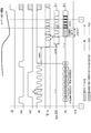
- FIG. 1 is a configuration diagram conceptually showing the overall configuration of the memory system 1 of the present embodiment.
- the memory system 1 of the present embodiment includes at least a semiconductor memory 3 and a memory controller (controller) 2 that controls the semiconductor memory 3.
- the semiconductor memory 3 may be a non-volatile memory, and for example, a NAND flash memory is suitable.
- NAND flash memory is suitable.
- memory controllers 2 and the NAND flash memory 3 it is possible to combine these memory controllers 2 and the NAND flash memory 3 to form one semiconductor device. Examples thereof include memory cards such as SD TM cards and SSDs (solid state drives). Further, the memory controller 2 can use a SoC (system on chip) or the like.
- SoC system on chip
- the NAND flash memory 3 includes a plurality of memory cell transistors and stores data non-volatilely.
- the memory controller 2 is connected to the NAND flash memory 3 by the NAND bus. Further, the memory controller 2 is also connected to the external host device 4 by the host bus.
- the memory controller 2 controls the NAND flash memory 3 and accesses the NAND flash memory 3 in response to an instruction received from the host device 4.
- the host device 4 is, for example, a digital camera, a personal computer, or the like, and the host bus is, for example, a bus that follows an SDTM interface.
- the NAND bus sends and receives signals according to the NAND interface.
- the memory controller 2 controls the NAND flash memory 3. As a specific example, the memory controller 2 controls to write data to the NAND flash memory 3 and read the already stored data from the NAND flash memory 3.
- the memory controller 2 includes a host interface circuit (host I / F) 5, a built-in memory (RAM: Random Access Memory) 6, a processor (CPU: Central Processing Unit) 7, a buffer memory 8, and a NAND interface circuit (NAND I / F) 9. , And an ECC (Error Checking and Correcting) circuit 10. Further, various other constituent parts are mounted depending on the design.
- host I / F host interface circuit
- RAM Random Access Memory
- processor CPU: Central Processing Unit
- NAND I / F NAND interface circuit
- ECC Error Checking and Correcting
- the host interface circuit 5 is connected to the host device 4 via the host bus, and transfers the instructions and data received from the host device 4 to the processor 7 and the buffer memory 8, respectively. Further, the data in the buffer memory 8 is transferred to the host device 4 in response to the instruction of the processor 7.
- the processor 7 controls the operation of the entire memory controller 2. For example, when the processor 7 receives a data write instruction from the host device 4, the processor 7 issues a write instruction to the NAND interface circuit 9 in response to the reception. The same applies when reading and erasing data. Further, the processor 7 executes various processes for managing the NAND flash memory 3, such as wear leveling.
- the operation of the memory controller 2 described below may be realized by the processor 7 executing software (firmware), or may be realized by hardware.
- the NAND interface circuit 9 is connected to the NAND flash memory 3 via the NAND bus and controls communication with the NAND flash memory 3. Then, the NAND interface circuit 9 transmits and receives various signals to the NAND flash memory 3 based on the instruction received from the processor 7.
- the buffer memory 8 temporarily holds write data and read data.
- the built-in memory (RAM) 6 is, for example, a semiconductor memory such as a DRAM or SRAM, and is used as a work area of the processor 7.
- the built-in memory 6 holds firmware for managing the NAND flash memory 3, various management tables, and the like.
- the ECC circuit 10 performs error detection and error correction processing on the data stored in the NAND flash memory 3. That is, the ECC circuit 10 generates an error correction code when writing data, assigns it to the written data, and decodes the error correction code when reading the data.
- the NAND bus will be described with reference to FIG.
- the memory controller 2 and the NAND flash memory 3 are connected by a NAND bus.
- the NAND bus includes a plurality of signal lines, and includes a signal line group connected to the input / output pad group 21 connected to the input / output circuit 12 and a signal line connected to the logic control pad group 22 connected to the logic control circuit 13. Divided into groups.
- These signal lines include chip enable signal / CE, command latch enable signal CLE, address latch enable signal ALE, write enable signal / WE, read enable signal / RE, write protect signal / WP, and ready signal according to the NAND interface.
- the busy signal / RB, the data signal DQ, the data strobe signal DQS, and / DQS are transmitted and received.
- the signals CLE, ALE, / WE, / RE, and / WP are received by the NAND flash memory 3. Further, the signal / RB and the signal / CE are each received by the NAND flash memory 3.
- the chip enable signal / CE is a signal for enabling the NAND flash memory 3.
- the command latch enable signal CLE makes it possible to latch the command CMD transmitted as the data signal DQ to the command register 15A of the register 15 described later.
- the signal CLE notifies the NAND flash memory 3 that the signal DQ flowing through the NAND flash memory 3 is the command CMD while the signal CLE is at the “H (High)” level.
- the signal DQ is, for example, an 8-bit signal.
- the address latch enable signal ALE makes it possible to latch the address ADD transmitted as the data signal DQ to the address register 15B of the register 15 described later.
- the signal ALE notifies the NAND flash memory 3 that the signal DQ transmitted to the NAND flash memory 3 is the address ADD while the signal ALE is at the “H” level.
- the write enable signal / WE enables writing.
- the signal / WE instructs the NAND flash memory 3 to capture the signal DQ transmitted to the NAND flash memory 3 while the signal / WE is at the “L (Low)” level.
- the read enable signals RE and / RE are used to instruct the NAND flash memory 3 to output the data signal DQ, and for example, to control the operation timing of the NAND flash memory 3 when outputting the signal DQ.
- the write protect signal / WP instructs the NAND flash memory 3 to prohibit data writing and erasing.
- the ready / busy signal / RB indicate whether the NAND flash memory 3 is in a ready state (a state in which an external instruction is accepted) or a busy state (a state in which an external instruction is not accepted), respectively.
- the data signal DQ is, for example, an 8-bit signal.
- the signal DQ is an entity of data transmitted / received between the NAND flash memory 3 and the memory controller 2, and includes a command CMD, an address ADD, and a data DAT.
- the bidirectional data strobe signals DQS and / DQS used as reference signals are used, for example, to control the operation timing of the NAND flash memory 3 related to the signal DQ.
- the NAND flash memory 3 includes a memory cell array 11, an input / output circuit 12, a logic control circuit 13, a register 15, a sequencer 16, a voltage generation circuit 17, a driver 18, a row decoder 19, a sense amplifier 20, an input / output pad group 21, and the like. It also includes a logic control pad group 22, a data generation circuit 14, and the like.
- the memory cell array 11 includes a plurality of blocks BLK (BLK0, BLK1, ).
- the block BLK includes a plurality of non-volatile memory cell transistors (not shown) associated with word lines and bit lines.
- the block BLK is, for example, a data erasing unit, and the data in the same block BLK is erased all at once.
- Each block BLK includes a plurality of string units SU (SU0, SU1, ).
- Each string unit SU includes a plurality of NAND strings NS.
- the number of blocks in the memory cell array 11 and the number of string units US in one block BLK and the number of NAND strings in one string unit SU can be set to any number.
- FIG. 3 shows a circuit of one block BLK in the memory cell array 11.
- each string unit SU is composed of a set of NAND strings NS.
- Each of the NAND strings NS includes, for example, 64 memory cell transistors MT (MT0 to MT63), a selection transistor ST1, and a selection transistor ST2.
- the number of memory cell transistors MT included in one NAND string NS is not limited to 64, and may be 8, 16, 96, or the like, and the number is not limited.
- the memory cell transistor MT includes a laminated gate including a control gate and a charge storage layer. Each memory cell transistor MT is connected in series between the selection transistors ST1 and ST2.
- the connection in the following description is not limited to an electrical connection in which the elements to be connected are in contact with each other, but also another conductive element between at least two elements, for example, wiring (metal wiring, polysilicon wiring, etc.). ) Intervenes.
- the gates of the selection transistors ST1 of the string units SU0 to SU3 are connected to the selection gate lines SGD0 to SGD3, respectively. Further, the gates of the selection transistors ST2 of all the string units SU in the block BLK are commonly connected to the selection gate line SGS.
- the control gates of the memory cell transistors MT0 to MT7 in the same block BLK are connected to the word lines WL0 to WL7, respectively. That is, the word line WL of the same address is commonly connected to all string units SU in the same block BLK, and the selected gate line SGS is commonly connected to all string units SU in the same block BLK. There is.
- the selection gate line SGD is connected to only one of the string units SU in the same block BLK.
- the other end of the selection transistor ST1 of the NAND string NS in the same row is m bit lines BL (BL0 to BL (m-1)). (M is a natural number)).
- the bit line BL is commonly connected to the NAND string NS in the same row over a plurality of blocks BLK.
- the other end of the selection transistor ST2 is connected to the source line SL.
- the source line SL is commonly connected to a plurality of NAND strings NS over a plurality of blocks BLK.
- data erasure is performed collectively for the memory cell transistors MT in the same block BLK, for example.
- the data read operation and the data write operation collectively perform the data read operation and the write operation for a plurality of memory cell transistors MT commonly connected to any word line WL in any string unit SU of any block BLK. Can be done.
- Such a set of memory cell transistors MT sharing a word line WL in one string unit SU is referred to as, for example, a cell unit CU. That is, the cell unit CU is a set of memory cell transistors MT capable of collectively executing a write operation or a read operation.
- one memory cell transistor MT can hold, for example, a plurality of bit data. Then, in the same cell unit CU, a set of 1 bits held by each of the memory cell transistors MT in the same bits is called a "page". That is, the "page" can also be defined as a part of the memory space formed in the set of memory cell transistors MT in the same cell unit CU.
- One page is, for example, 128 Kbit (16 KByte).
- the input / output circuit 12 includes at least an input circuit 12A, an output circuit 12B, and a control circuit 12C.
- the input / output circuit 12 transmits / receives a data signal DQ to / from the memory controller 2.
- the input / output circuit 12 transfers the command CMD and the address ADD included in the signal DQ input to the input / output pad group 21 to the command register 15A and the address register 15B of the register 15, respectively.
- the input / output circuit 12 transfers the write data DAT included in the signal DQ input to the input / output pad group 21 to the data register 20B of the sense amplifier 20, and is also transferred from the data register 20B of the sense amplifier 20.
- the read data DAT is transferred to the input / output pad group 21.
- FIG. 4 is a circuit diagram of the output circuit 12B.
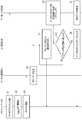
- the output circuit 12B includes a shift register unit 31A and a multiplexer (MUX) 31D [selection circuit].
- the shift register unit 31A includes a shift register 31B [holding circuit] composed of a plurality of flip-flops 31C connected in series.
- the shift register 31B is arranged in each of the signal lines DQ0 to DQ7, and temporarily holds data in each of the signal lines DQ0 to DQ7.
- the number of flip-flops 31C is appropriately set according to the timing control of the signal DQ, and is, for example, eight.
- One of the plurality of input terminals of the multiplexer 31D is connected to the input terminal D of the flip-flop 31C of the first stage (on the rightmost side of the paper in FIG. 4), and the output terminal Q thereof is the input terminal of the flip-flop 31C of the next stage. Connected to D.
- the output terminal Q of the next-stage flip-flop 31C is connected to the input terminal D of the next-stage flip-flop 31C, and is similarly connected thereafter.
- the output terminal Q of the flip-flop 31C in the final stage is connected to one of the signal lines DQ0 to DQ7 (signal line DQ0 in the example of FIG. 4).
- internal clocks iCLK having different cycles are input from the sequencer 16 to the clock terminals of the flip-flops 31C.
- Each flip-flop 31C latches the input data at the timing when the internal clock iCLK input to each clock terminal rises.
- the multiplexer 31D selects 8 bits of the read data DAT of one page (16KBbyte) read from the memory cell array 11 into the sense amplifier unit 20A and stored in the data register 20B, and transfers the data to the shift register unit 31A. ..
- the transferred 8-bit data is sequentially transferred while being held by the flip-flop 31C that functions as a buffer.
- the memory controller 2 toggles the read enable signals RE and / RE after the read data is temporarily held by the shift register 31B
- the read data held by the shift register 31B is transferred to the final stage flip-flop 31C. It is output as DQ data by 8 bits from the output terminal Q. That is, the output circuit 12B converts the 16KByte parallel data into 8-bit serial data.
- the logic control circuit 13 receives signals / CE, CLE, ALE, / WE, / RE, and / WP from the memory controller 2. Further, the logic control circuit 13 transfers the signal / RB to the memory controller 2 and notifies the memory controller 2 whether the NAND flash memory 3 is in the ready state or the busy state.
- the logic control circuit 13 includes a correction circuit 13a including a phase-locked loop (PLL) circuit or a delay-locked loop (DLL) circuit.
- the correction circuit 13a has a function of correcting the duty ratios of the signals RE and / RE, which are input respectively, via the pads in the logic control pad group.
- the correction circuit 13a corrects the duty ratios of the signals RE and / RE based on the control signal from the sequencer 16, and generates the corrected signals RE and / RE.
- the corrected signals RE and / RE are sent to, for example, the input / output circuit 12, and the input / output circuit 12 toggles the signals DQS and / DQS at the timing corresponding to the corrected signals RE and / RE.
- the register 15 includes a command register 15A that holds a command CMD and an address register 15B that holds an address ADD.
- the register 15 transfers the address ADD to the low decoder 19 and the sense amplifier 20, and also transfers the command CMD to the sequencer 16.
- the sequencer 16 receives the command CMD and controls the entire NAND flash memory 3 according to the sequence based on the received command CMD. Further, the sequencer 16 sends the temperature information received from the temperature sensor or the like to the memory controller 2 via the input / output circuit 12.
- the voltage generation circuit 17 generates a voltage necessary for operations such as writing, reading, and erasing data based on an instruction from the sequencer 16.
- the voltage generation circuit 17 supplies the generated voltage to the driver (driver set) 18.
- the driver 18 supplies various voltages from the voltage generation circuit 17 to the low decoder 19 and the sense amplifier 20 based on the address ADD transferred from the address register 15B of the register 15.
- the driver 18 supplies various voltages to the row decoder 19 based on, for example, the row address in the address.
- the row decoder 19 receives the row address included in the address ADD transferred from the address register 15B of the register 15, and selects the memory cell transistor in the row based on the row address. Then, the voltage from the driver 18 is transferred to the memory cell transistor in the selected row via the row decoder 19.
- the sense amplifier 20 includes a sense amplifier unit 20A and a data register 20B. At the time of reading data, for example, the sense amplifier unit 20A reads (senses) the read data DAT read from the memory cell transistor into the bit line, and transfers the read read data DAT to the data register 20B. The read data DAT held in the data register 20B is transferred to the output circuit 12B.
- the write data DAT to which the write data DAT is transferred from the input circuit 12A to the data register 20B is written to the memory cell transistor by the sense amplifier unit 20A via the bit line.
- the sense amplifier 20 receives the column address included in the address ADD from the address register 15B of the register 15, and outputs column data based on the column address.
- the sense amplifier unit 20A reads data from the memory cell transistor and transfers the data to the data register 20B in response to the read command given by the memory controller 2, and the data corresponds to the data out command given by the memory controller 2.
- the data held by the register 20B is transferred to the output circuit 12B.
- period tR The period from when the read command is given from the memory controller 2 until the sense amplifier 20A reads the data from the memory cell array 11 and the read data is held in the data register 20B is called "period tR". During the period tR, both the ready busy signal R / Bn and the internal busy signal are at the “L” level (ready state).
- the input / output pad group 21 transfers the data signals DQ, DQS, and / DQS received from the memory controller 2 to the input / output circuit 12. Further, the input / output pad group 21 transfers the signal DQ transmitted from the input / output circuit 12 to the outside of the NAND flash memory 3.
- the logic control pad group 22 transfers the signals / CE, CLE, ALE, / WE, / RE, and / WP received from the memory controller 2 to the logic control circuit 13. Further, the logic control pad group 22 transfers / RB transmitted from the logic control circuit 13 to the outside of the NAND flash memory 3.
- the data generation circuit 14 outputs dummy data from the output circuit 12B in response to the signals DQS and / DQS, for example, based on an instruction from the sequencer 16. Specifically, the memory controller 2 toggles the read enable signals RE and / RE, and the NAND flash memory 3 receives the signals RE and / RE to generate signals DQS and / DQS. The data generation circuit 14 receives the signals DQS and / DQS, generates preset dummy data, and outputs the dummy data from the output circuit 12B to the memory controller 2. When the memory controller 2 determines that the received data is dummy data, the memory controller 2 does not process the data or processes the received data as invalid data.
- the dummy data may be, for example, a random pattern.
- the dummy data may be a pattern in which each signal of the signal lines DQ0 to DQ7 repeatedly toggles at the "H" level and the "L" level, such as 55h-AAh-55h-AAh ... , It may be a fixed value data pattern.
- the data generation circuit 14 may be included in the logic control circuit 13 or the input / output circuit 12.
- the control circuit 12C of the input / output circuit 12 may have a function as a data generation circuit 14.
- FIG. 4 shows a configuration example of the output circuit 12B.
- FIG. 6A shows a data read timing chart according to the comparative example
- FIG. 6B shows a data read timing chart according to the present embodiment.
- FIG. 6A shows the standby time tWHR2 and the delay time (latency) set in the NAND flash memory 3 in the comparative example.
- the NAND flash memory 3 according to the comparative example has the same circuit configuration as the NAND flash memory 3 according to the present embodiment, but the operation related to the standby time t WHR2 and the delay time is different.
- the sense amplifier unit 20A of the sense amplifier 20 reads the data of one page (for example, 16KByte) from the memory cell array 11, and the data register 20B sets the data register 20B. Stores the read data.
- a data out command is issued from the memory controller 2 to the NAND flash memory 3.
- the data-out command includes, for example, one or more command signals (“05h” and “” E0h) given as an 8-bit signal DQ and one or more address signals (column address ADD) given as an 8-bit signal DQ. And a low address ADD), which is a command set.
- the standby time t WHR2 [first period]
- the read data of 16KByte read from the memory cell array 11 is output from the data register 20B. It is the time required for the data to be transferred to the circuit 12B and for the output circuit 12B to complete the preparation for outputting the first 8 bits as DQ data to the memory controller 2.
- Data may be output. That is, in the comparative example, the memory controller 2 issues a data out command to the NAND flash memory 3 and then waits for the standby time t WHR2 before instructing the NAND flash memory 3 to output data. Cannot toggle the signals RE and / RE for.
- a delay time (latency) [second period] is further added after the waiting time t WHR2 [first period] has elapsed.
- the signals DQS and / DQS transmitted from the NAND flash memory 3 also start toggling with a delay of the period t DQSRE.
- the correction circuit 13a of the logic control circuit 13 described above corrects the duty ratio of the signals RE and / RE input from the memory controller 2 via the logic control pad group 22, and the input / output circuit 12 is corrected.
- the signals DQS and / DQS are generated based on the signals RE and / RE.
- the signals DQS and / DQS are used, for example, to control the operation timing of the NAND flash memory 3 related to the signal DQ. Therefore, the NAND flash memory 3 can start outputting valid data as soon as the signals DQS and / DQS start toggling, for example. However, immediately after the memory controller 2 starts toggling the signals RE and / RE, the power supply VDD of the NAND flash memory 3 may become unstable. Therefore, for example, the above-mentioned delay time is set in order to suspend the output of valid data until the power supply VDD, which has become unstable due to the start of the toggle of the signals RE and / RE, is stabilized.
- the timing at which the output of valid data is started is delayed by a delay time from the timing at which the toggle of the signals DQS and / DQS is started.
- This delay time is preferably a long time for stabilizing the power supply VDD, but is preferably a short time for speeding up the operation.
- the delay time is set in order to secure the time required for correction processing by a phase lock loop (PLL) or delay lock loop (DLL) provided in the correction circuit (DCC) 13a, for example, duty ratio correction or timing correction. It may be set.
- PLL phase lock loop
- DLL delay lock loop
- the sequencer 16 counts either one of the signals RE and / RE, or one of the signals DQS and / DQS, and after reaching a predetermined number of counts, transfers the data register 20B to the output circuit 12B. Starts the output of the data (valid data).
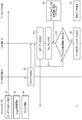
- FIG. 5 is a flowchart showing data output in the comparative example.
- the sense amplifier unit 20A of the sense amplifier 20 reads data from the memory cell array 11, for example, data of 16 KBbyte per page by a read command issued from the memory controller 2 in advance, and the data register 20B reads the data. It is assumed that the data is stored.
- the memory controller 2 issues a data out command via the data signal lines DQ0 to DQ7 while toggle the signal / WE (step S1). This command is output to the sense amplifier 20, and the preset time measurement is started from the time when the signal / WE toggle is stopped (step S2).
- read data is transferred from the data register 20B to the multiplexer 31D in the output circuit 12B (step S3).
- the multiplexer 32D selects, for example, 16 KBbyte data by 8 bits and transfers the data to the shift register unit 31A.
- this standby time t WHR2 step S4: NO
- step S4 when the period of the standby time t WHR2 ends (step S4: YES), the output circuit 12B is ready to output data to the memory controller 2, so that the memory controller 2 receives the read enable signal RE and Toggle / RE is started (step S5).
- the NAND flash memory 3 that has received the toggle of the signals RE and / RE starts the toggle of the signals DQS and / DQS.
- the data generation circuit 14 that has received the toggle of the signals DQS and / DQS outputs the dummy data set in advance from the output circuit 12B.
- the output circuit 12B outputs invalid dummy data to the signal lines DQ0 to DQ7 during the preset delay time, and is stored in the shift register unit 31A after the end of the preset delay time.
- the data is output to the signal lines DQ0 to DQ7 (step S6).
- data can be continuously transferred from the data register 20B to the multiplexer 31D of the output circuit 12B (step S7). Further, data is output from the output circuit 12B to the memory controller 2.
- the time from when the memory controller 2 issues the data out command until the first valid 8-bit data is output from the NAND flash memory 3 is at least inside the NAND flash memory 3. It includes the waiting time t WHR2 required for the data transfer process and the delay time required to wait for the unstable power supply VDD to stabilize in response to the toggle of the signals RE and / RE. For example, if the delay time is short, the data output is started before the output of the power supply VDD becomes stable, so that the level of the output data may become unstable.
- the memory controller 2 starts the toggle of the signal RE and / RE after the waiting time t WHR2 ', which is shorter than the waiting time t WHR2 required for the internal data transfer processing in the NAND flash memory 3, elapses. .. Then, in the NAND flash memory 3, the input / output circuit 12 generates signals DQS and / DQS based on the signals RE and / RE received from the memory controller 2 and outputs them to the output circuit 12B, and also outputs the data generation circuit 14 Generates dummy data based on the signals DQS and / DQS and outputs the dummy data to the output circuit 12B. The output circuit 12B outputs dummy data to the memory controller 2 during the delay time. The memory controller 2 does not correspond to the received dummy data. Instead, the output of the power supply is stabilized.
- the dummy data may be, for example, a random pattern or a preset data pattern, and is not particularly limited.
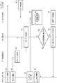
- Step S1 the memory controller 2 issues a read command in advance, and the desired data is read from the memory cell array 11 and stored in the data register 20B.
- Step S1 the memory controller 2 issues a data out command to the NAND flash memory 3.
- This data out command is a command set including a first command signal "05h” given as an 8-bit signal DQ, a column address signal ADD, a low address signal ADD, and a second command signal "E0h".
- the memory controller 2 toggles the signal / WE in a cycle of time t WC in accordance with the issuance of the data out command.
- the memory controller 2 issues a data out command and starts time measurement (step S2). Then, the memory controller 2 toggles the signals RE and / RE in a cycle of time t RC within the period of the waiting time t WHR2, that is, after the elapse of t WHR2'which is shorter than the waiting time t WHR2 (step). S5).
- the number of times the signals RE and / RE are toggled and the toggle start timing within the period of the standby time t WHR2 can be appropriately set by, for example, a set feature.
- the data of, for example, 16 KBbyte held by the data register 20B is transferred to the multiplexer 31D in the input / output circuit 12 (step S3).
- the multiplexer 31D transfers, for example, 16 KBbyte data to each shift register 31B of the shift register unit 31A by 8 bits at a time.
- the toggle of the signals DQS and / DQS is started in the NAND flash memory 3 with a delay of the period t DQSRE'.
- the data generation circuit 14 generates dummy data after the start of toggle of the signals DQS and / DQS, and outputs the dummy data to the output circuit 12B (step S8).
- the output circuit 12B outputs dummy data together with the signals DQS and / DQS to the memory controller 2 during the delay time provided in advance (step S11).
- FIG. 6B an example is shown in which the toggle of the signals DQS and / DQS starts and the output of dummy data starts.
- timings are not limited. As described above, the memory controller 2 does not process the dummy data. Further, since the timing of starting the toggle of the signals RE and / RE is advanced, the output of the power supply VDD is more stable at the timing when the output of valid data other than dummy data is started.
- step S12 when the number of toggles of the signal DQS reaches the set number of times (step S12: YES), the data signal DQ read from the shift register unit 31A of the output circuit 12B to the memory controller 2 is output (step S6). In cooperation with this output, data can be continuously transferred from the data register 20B to the multiplexer 31D of the output circuit 12B (step S7). Further, data is output from the output circuit 12B to the memory controller 2. Further, the output time or the number of cycles (the number of toggles) of the dummy data in the signal DQ is appropriately set and is not limited. In the comparative example shown in FIG.
- the toggle of the signals RE and / RE is started, and then the toggle of the signals DQS and / DQS is started. Further, the timing at which the output of valid data is started is delayed by a delay time from the timing at which the toggle of the signals DQS and / DQS is started.
- the power supply VDD becomes unstable due to the start of toggle of the signals RE and / RE, the output of effective data can be started after the power supply VDD becomes stable by setting the delay time long.
- the time from when the memory controller 2 issues the data out command until the first valid 8-bit data is output from the NAND flash memory 3 is at least the standby time t WHR2 . It is longer than the sum of the delay times.
- the toggle of the signal RE and / RE [first signal] is started during the waiting time t WHR 2 [first period] shown in FIG. 6B, followed by the signal DQS. And / DQS [second signal] toggle is initiated.
- the data generation circuit 14 generates dummy data [first data] after an arbitrary number of toggles of the signals DQS and / DQS has elapsed, and outputs the dummy data [first data] from the output circuit 12B to the memory controller 2.
- the memory controller 2 does not treat the dummy data as valid data (data read from the memory cell array 11 and stored in the data register 20B), and does not perform data processing.
- the memory controller 2 can determine whether or not the data is dummy data based on, for example, the number of times the signal DQS is toggled.
- the dummy data has a pattern of repeating toggles such as 55h-AAh-55h-AAh ..., it may be determined whether or not the dummy data is dummy data based on the number of times the dummy data is toggled instead of the number of times the signal DQS is toggled. ..
- the toggle of the signals RE and / RE and the toggle of the signals DQS and / DQS are continuously started during the waiting time t WHR2, and then dummy data is output. Therefore , the standby time t WHR2 and the delay time can be overlapped in time, and the output of the power supply VDD can be stabilized from an earlier stage than in the comparative example. Therefore, when the timing at which the output of valid data is started is set to the same timing as the comparative example described with reference to FIG. 6A, the delay time (latency) for stabilizing the output of the power supply is set longer. can do. Thereby, for example, as shown in FIG. 6B, it is possible to start the output of valid data after the output of the power supply VDD becomes stable, and it is possible to improve the read reliability of the data.
- the signal RE and / RE toggle is started from an earlier stage.
- Signals DQS and / DQS are toggled and the delay time at which dummy data is output ends earlier, so the timing at which valid data output starts is earlier than in the comparative example, and the actual data The read time can be increased.
- the timing at which the memory controller 2 starts toggling the signals RE and / RE with respect to the standby time t WHR2 , or the timing at which the output of dummy data ends and the output of valid data starts is shown in the first embodiment.
- the setting is not limited to that shown in 6B, and can be appropriately set according to the design and device specifications. An example of timing setting will be described below.
- the toggle of the signals RE and / RE starts within the waiting time t WHR2 , the toggle of the signals DQS and / DQS is started so as to follow immediately after that, and the output of the dummy data in the signal DQ is started.
- the toggle of the signals RE and / RE and the toggle of the signals DQS and / DQS are continuously performed at least until the end of the output of the dummy data in the signal DQ.
- the standby time t WHR2 is set to 300 nsec
- the toggle of the signal RE and / RE is set to 2.5 nsec for one cycle time t RC.
- these time settings are not limited, and can be appropriately set by the memory controller 2.
- the time can be set in the same way for other setting examples.
- the second setting example shown in FIG. 9 is set at the timing of ending the dummy data in the delay time (latency) after the toggle of the waiting time t WHR2 is completed. It is the same as the first embodiment described above. In the second setting example, the timing can be set more easily than in the first setting example. Also in this second setting example, the standby time t WHR2 is set to 300 nsec, and the toggle of the signal RE and / RE is set to 2.5 nsec for one cycle time t RC.
- the toggle of the signals RE and / RE and the toggle of the signals DQS and / DQS are started, and the output of dummy data is started. Further, within the waiting time t WHR2 , the signals RE and / RE and the signals DQS and / DQS that have reached the set number of toggles terminate the toggle, but the output of dummy data in the signal DQ is continued. .. Then, it waits for the toggle of the signals RE and / RE to start the data output.
- the toggle of the signals RE and / RE and the signals DQS and / DQS is restarted, and the output of the dummy data in the signal DQ ends.
- the standby time t WHR2 is set to 300 nsec
- the toggle of the signals RE and / RE is set to 2.5 nsec for one cycle time t RC.
- the power consumption can be suppressed.
- the standby time t WHR2 is set to 300 nsec
- the toggle of the signals RE and / RE is set to 2.5 nsec for one cycle time t RC.
- the power consumption can be suppressed as in the third setting example.
- the memory controller 2 starts the signal / WE toggle and issues the address ADD and the data out command (step S1).
- the data stored in the data register 20B is transferred to the multiplexer 31D in the input / output circuit 12 (step S3).
- the multiplexer 31D stores, for example, 16 KBbyte data in each shift register 31B by 8 bits at a time.
- the memory controller 2 starts the time measurement from the time when the data out command is issued and the signal / WE toggle is stopped (step S2). Then, within the period of the waiting time t WHR2 , the memory controller 2 starts the toggle of the waiting time t RC for one cycle of the signals RE and / RE (step S4).
- the NAND flash memory 3 starts toggle the signals DQS and / DQS after a set amount of time.
- the data generation circuit 14 After starting to toggle the signals DQS and / DQS, the data generation circuit 14 generates dummy data and outputs it to the output circuit 12B (step S8).
- the output circuit 12B outputs dummy data together with the signals DQS and / DQS to the memory controller 2 via the signal lines DQ0 to DQ7 (step S11).
- the duty ratio correction process by the PLL / DLL provided in the correction circuit 13a of the logic control circuit 13 is performed (step S13).
- the data stored in the data register 20B is transferred to the multiplexer 31D (step S3).
- the multiplexer 31D stores, for example, 16 KBbyte data in each shift register 31B by 8 bits at a time.
- step S12 YES
- the toggle of the signal DQS reaches the set number of times (or the output time of the toggle) (step S12: YES)
- step S12 the output time of the toggle
- the data read into the shift register 31B Is started to be output to the memory controller 2 (step S6).
- step S6 data can be continuously transferred from the data register 20B to the multiplexer 31D of the output circuit 12B (step S7). Further, data can be output from the output circuit 12B to the memory controller 2.
- the present embodiment by stabilizing the output of the power supply from an earlier stage than in the comparative example, it is possible to start the data output after stabilizing the output of the power supply. Further, the latency can be set longer in order to stabilize the output of the power supply from an early stage. Therefore, it is possible to secure the time for performing other processing such as the duty ratio correction processing within the delay time. Further, by performing these correction processing times by utilizing the standby time and the delay time, a sufficient processing time can be used and the accuracy of the correction can be improved.
- This embodiment is a flow in which the issuance of the data out command in the first embodiment described above and the step of starting the toggle of the signal RE and / RE are interchanged. That is, the data out command is issued after the toggle of the signals RE and / RE is started first.
- the memory controller 2 starts toggling the signals RE and / RE (step S5). After that, the memory controller 2 issues an address ADD and a data out command (step S1). After issuing the data out command, the memory controller 2 starts time measurement (step S2). The memory controller 2 starts toggle of signals DQS and / DQS after a preset time or the number of times of toggle of signals RE and / RE elapses within a period of standby time t WHR2 after the start of measurement. , When the signal DQS and / DQS toggle is started, the data generation circuit 14 generates dummy data and outputs it to the output circuit 12B (step S8).
- the output circuit 12B outputs dummy data together with the signals DQS and / DQS to the memory controller 2 via the signal lines DQ0 to DQ7 during the delay time (step S11). Also in this embodiment, the memory controller 2 determines that the received data is dummy data and does not process it.
- the data stored in the data register 20B is transferred to the multiplexer 31D in the input / output circuit 12 (step S3).
- the multiplexer 31D stores, for example, 16 KBbyte data in each shift register 31B by 8 bits at a time.
- step S12 when the toggle of the signal DQS reaches the set number of times (step S12: YES), that is, when the delay time (latency) ends, data is transmitted from the shift register unit 31A of the output circuit 12B to the memory controller 2. It is output (step S6). In cooperation with this output, data can be continuously transferred from the data register 20B to the multiplexer 31D of the output circuit 12B (step S7). Further, data can be output from the output circuit 12B to the memory controller 2.
- this embodiment can obtain the same effect as that of the first embodiment described above. Further, in the present embodiment, the timing of issuing the data out command and the start of the toggle of the signals RE and / RE is not specified, and the data out command is issued after the start of the toggle of the signals RE and / RE. May be good. Also in this embodiment, the data is read from the memory cell array 11 by the sense amplifier 20 and transferred to the multiplexer 31D of the output circuit 12B at the same time or in parallel during the standby time and the period during which the dummy data is output. Since it can be processed, the power supply can be stabilized and appropriate data can be output.
- the toggle of the signals RE and / RE is started, and then the data out command is issued.
- the memory controller 2 issues a read command to the NAND flash memory 3 together with the address ADD and the like (step S14).
- the sense amplifier unit 20A reads data from the memory cell array 11 and stores it in the data register 20B (step S15). At the same time, the memory controller 2 initiates the toggle of the signals RE and / RE (step S5).
- the NAND flash memory 3 starts the toggle of the signals DQS and / DQS after the toggle of the signals RE and / RE is started.
- the data generation circuit 14 After starting to toggle the signals DQS and / DQS, the data generation circuit 14 generates dummy data and outputs it to the output circuit 12B (step S8).
- the output circuit 12B outputs dummy data together with the signals DQS and / DQS to the memory controller 2 via the signal lines DQ0 to DQ7 (step S11). Also in this embodiment, even if the dummy data is output from the output circuit 12B to the memory controller 2, it is determined to be invalid data and is not processed.
- the memory controller 2 issues a data out command to the NAND flash memory 3 (step S1). After issuing the data out command, the memory controller 2 starts time measurement (step S2). Within the period of the standby time t WHR2, the data stored in the data register 20B is transferred to the multiplexer 31D of the output circuit 12B (step S3). For example, the multiplexer 31D initially stores 16 KBbyte data in each shift register 31B by 8 bits.
- step S12 when the toggle of the signal DQS reaches the set number of times (step S12: YES), that is, when the delay time (latency) ends, data is transmitted from the shift register unit 31A of the output circuit 12B to the memory controller 2. It is output (step S6). In cooperation with this output, data can be continuously transferred from the data register 20B to the multiplexer 31D of the output circuit 12B (step S7). Further, data can be output from the output circuit 12B to the memory controller 2.
- this embodiment can obtain the same effect as that of the first embodiment described above. Further, in the present embodiment, the toggle of the signals RE and / RE can be started during the period after the issuance of the read command and before the issuance of the data out command.
- a get feature command is used to output a preset set value in the NAND flash memory 3. Specifically, as shown in FIG. 15, when the memory controller 2 issues the read command XXh of the get feature command, the period corresponding to the above-mentioned waiting time t WHR2 (time t WB + set time t FEAT + time t).
- the toggle of the signals RE and / RE is started, and the NAND flash memory 3 starts the toggle of the signals DQS and / DQS correspondingly.
- the data generation circuit 14 After starting to toggle the signals DQS and / DQS, the data generation circuit 14 generates dummy data and outputs it to the output circuit 12B.
- the output circuit 12B outputs dummy data to the memory controller 2 via the signal lines DQ0 to DQ7.
- the NAND flash memory 3 outputs the set value to the memory controller 2 after the output of the dummy data is completed.
- the NAND flash memory 3 of the present embodiment has a set time t FEAT , timing of start and end of toggle of signals RE and / RE, timing of start and end of toggle of signals DQS and / DQS, number of times of each toggle, and /
- each set value of the dummy data output time (when the dummy data is a pattern that repeats toggles such as 55h-AAh-55h-AAh ..., the number of toggles) is held in a feature register (not shown in advance).
- a feature register not shown in advance.
Abstract
A memory system according to an embodiment outputs read enable signals RE and/RE, during a waiting time tWHR2 taken for a process for outputting signals to a controller, and outputs from an output circuit, dummy data preset in signals DQS and /DQS and a signal DQ.
Description
実施形態は、メモリシステムに関する。
The embodiment relates to a memory system.
半導体記憶装置としてのNAND型フラッシュメモリが知られている。
NAND flash memory as a semiconductor storage device is known.
データの読み出し信頼性を向上できるメモリシステムを提供する。
Provide a memory system that can improve the read reliability of data.
実施形態のメモリシステムは、半導体メモリと、前記半導体メモリからデータを読み出す指示を与えるコントローラと、を具備し、前記半導体メモリは、データを保持するメモリセルトランジスタと、前記メモリセルトランジスタから読み出されたデータに対して、前記コントローラへ出力するための処理を行う出力回路と、第1データを生成するデータ生成回路と、を備え、前記データの読み出し時において、前記コントローラは、前記出力回路が前記処理を行っている第1期間内に第1信号を前記半導体メモリへ出力し、前記半導体メモリは、前記第1信号に基づいて第2信号を生成し、第1期間と第2期間の期間に、前記第2信号と共に前記第1データを前記コントローラへ出力し、前記第2期間の終了後に前記半導体メモリは、前記第2信号と共に前記メモリセルトランジスタから読み出されたデータを前記コントローラへ出力する。
The memory system of the embodiment includes a semiconductor memory and a controller that gives an instruction to read data from the semiconductor memory, and the semiconductor memory is read from a memory cell transistor that holds data and the memory cell transistor. The controller includes an output circuit that performs processing for outputting the data to the controller and a data generation circuit that generates the first data. At the time of reading the data, the output circuit of the controller is the same. The first signal is output to the semiconductor memory within the first period during the processing, and the semiconductor memory generates a second signal based on the first signal during the first period and the second period. The first data is output to the controller together with the second signal, and after the end of the second period, the semiconductor memory outputs the data read from the memory cell transistor together with the second signal to the controller. ..
以下に、実施形態について図面を参照して説明する。
実施形態は、発明の技術的思想を具体化するための装置を例示する。図面は、模式的または概念的なものであり、各図面の寸法及び比率等は、必ずしも現実のものと同一とは限らない。また、構成要素の形状、構造、配置等によって、本発明の技術的思想が特定されるものではない。なお、以下の説明において、略同一の機能及び構成を有する構成要素については、同一符号を付して、詳細な説明は省略する。 Hereinafter, embodiments will be described with reference to the drawings.
The embodiment exemplifies an apparatus for embodying the technical idea of the invention. The drawings are schematic or conceptual, and the dimensions and ratios of each drawing are not necessarily the same as the actual ones. Further, the technical idea of the present invention is not specified by the shape, structure, arrangement, etc. of the constituent elements. In the following description, components having substantially the same function and configuration are designated by the same reference numerals, and detailed description thereof will be omitted.
[第1実施形態]
第1実施形態に係るメモリシステムについて説明する。
<メモリシステム全体構成>
図1は、本実施形態のメモリシステム1の全体構成を概念的に示す構成図である。
本実施形態のメモリシステム1は、少なくとも半導体メモリ3と、この半導体メモリ3を制御するメモリコントローラ(コントローラ)2と、を備えている。本実施形態では、半導体メモリ3は、不揮発性メモリであればよく、例えば、NAND型フラッシュメモリが好適する。以下の説明では、半導体記憶装置としてNAND型フラッシュメモリ3に適用した例について説明する。 [First Embodiment]
The memory system according to the first embodiment will be described.
<Overall memory system configuration>
FIG. 1 is a configuration diagram conceptually showing the overall configuration of thememory system 1 of the present embodiment.
Thememory system 1 of the present embodiment includes at least a semiconductor memory 3 and a memory controller (controller) 2 that controls the semiconductor memory 3. In the present embodiment, the semiconductor memory 3 may be a non-volatile memory, and for example, a NAND flash memory is suitable. In the following description, an example applied to the NAND flash memory 3 as a semiconductor storage device will be described.
第1実施形態に係るメモリシステムについて説明する。
<メモリシステム全体構成>
図1は、本実施形態のメモリシステム1の全体構成を概念的に示す構成図である。
本実施形態のメモリシステム1は、少なくとも半導体メモリ3と、この半導体メモリ3を制御するメモリコントローラ(コントローラ)2と、を備えている。本実施形態では、半導体メモリ3は、不揮発性メモリであればよく、例えば、NAND型フラッシュメモリが好適する。以下の説明では、半導体記憶装置としてNAND型フラッシュメモリ3に適用した例について説明する。 [First Embodiment]
The memory system according to the first embodiment will be described.
<Overall memory system configuration>
FIG. 1 is a configuration diagram conceptually showing the overall configuration of the
The
これらのメモリコントローラ2とNAND型フラッシュメモリ3とを組み合わせて、1つの半導体装置を構成することが可能である。その一例としては、SDTMカード等のメモリカードや、SSD(solid state drive)等がある。また、メモリコントローラ2は、SoC(system on chip)等を用いることができる。
It is possible to combine these memory controllers 2 and the NAND flash memory 3 to form one semiconductor device. Examples thereof include memory cards such as SD TM cards and SSDs (solid state drives). Further, the memory controller 2 can use a SoC (system on chip) or the like.
NAND型フラッシュメモリ3は、複数のメモリセルトランジスタを備え、データを不揮発に記憶する。メモリコントローラ2は、NANDバスによってNAND型フラッシュメモリ3に接続される。さらに、メモリコントローラ2は、ホストバスによって外部のホスト機器4とも接続する。このメモリコントローラ2は、NAND型フラッシュメモリ3を制御し、またホスト機器4から受信した命令に応答して、NAND型フラッシュメモリ3にアクセスする。ホスト機器4は、例えばデジタルカメラやパーソナルコンピュータ等であり、ホストバスは、例えばSDTMインターフェースに従ったバスである。NANDバスは、NANDインターフェースに従った信号の送受信を行う。
The NAND flash memory 3 includes a plurality of memory cell transistors and stores data non-volatilely. The memory controller 2 is connected to the NAND flash memory 3 by the NAND bus. Further, the memory controller 2 is also connected to the external host device 4 by the host bus. The memory controller 2 controls the NAND flash memory 3 and accesses the NAND flash memory 3 in response to an instruction received from the host device 4. The host device 4 is, for example, a digital camera, a personal computer, or the like, and the host bus is, for example, a bus that follows an SDTM interface. The NAND bus sends and receives signals according to the NAND interface.
<メモリコントローラ2の構成>
図1を参照して、メモリコントローラ2の構成の詳細について説明する。
メモリコントローラ2は、NAND型フラッシュメモリ3を制御する。具体例としては、メモリコントローラ2は、データをNAND型フラッシュメモリ3に書き込み、既に記憶されているデータをNAND型フラッシュメモリ3から読み出す制御を行う。 <Configuration ofmemory controller 2>
The details of the configuration of thememory controller 2 will be described with reference to FIG.
Thememory controller 2 controls the NAND flash memory 3. As a specific example, the memory controller 2 controls to write data to the NAND flash memory 3 and read the already stored data from the NAND flash memory 3.
図1を参照して、メモリコントローラ2の構成の詳細について説明する。
メモリコントローラ2は、NAND型フラッシュメモリ3を制御する。具体例としては、メモリコントローラ2は、データをNAND型フラッシュメモリ3に書き込み、既に記憶されているデータをNAND型フラッシュメモリ3から読み出す制御を行う。 <Configuration of
The details of the configuration of the
The
メモリコントローラ2は、ホストインターフェース回路(ホストI/F)5、内蔵メモリ(RAM:Random Access Memory)6、プロセッサ(CPU:Central Processing Unit)7、バッファメモリ8、NANDインターフェース回路(NANDI/F)9、及びECC(Error Checking and Correcting)回路10を備えている。さらに、設計に応じて、他にも種々の構成部位を搭載している。
The memory controller 2 includes a host interface circuit (host I / F) 5, a built-in memory (RAM: Random Access Memory) 6, a processor (CPU: Central Processing Unit) 7, a buffer memory 8, and a NAND interface circuit (NAND I / F) 9. , And an ECC (Error Checking and Correcting) circuit 10. Further, various other constituent parts are mounted depending on the design.
ホストインターフェース回路5は、ホストバスを介してホスト機器4と接続され、ホスト機器4から受信した命令及びデータを、それぞれプロセッサ7及びバッファメモリ8に転送する。またプロセッサ7の命令に応じて、バッファメモリ8内のデータをホスト機器4へ転送する。
The host interface circuit 5 is connected to the host device 4 via the host bus, and transfers the instructions and data received from the host device 4 to the processor 7 and the buffer memory 8, respectively. Further, the data in the buffer memory 8 is transferred to the host device 4 in response to the instruction of the processor 7.
プロセッサ7は、メモリコントローラ2全体の動作を制御する。例えば、プロセッサ7は、ホスト機器4からデータの書き込み命令を受信した際には、その受信に応じて、NANDインターフェース回路9に対して、書き込み命令を発行する。データの読み出し及び消去の際も同様である。また、プロセッサ7は、ウェアレベリング等、NAND型フラッシュメモリ3を管理するための様々な処理を実行する。なお、以下で説明するメモリコントローラ2の動作は、プロセッサ7がソフトウェア(ファームウェア)を実行することによって実現されてもよいし、またはハードウェアで実現されてもよい。
The processor 7 controls the operation of the entire memory controller 2. For example, when the processor 7 receives a data write instruction from the host device 4, the processor 7 issues a write instruction to the NAND interface circuit 9 in response to the reception. The same applies when reading and erasing data. Further, the processor 7 executes various processes for managing the NAND flash memory 3, such as wear leveling. The operation of the memory controller 2 described below may be realized by the processor 7 executing software (firmware), or may be realized by hardware.
NANDインターフェース回路9は、NANDバスを介してNAND型フラッシュメモリ3と接続され、NAND型フラッシュメモリ3との通信を司る。そしてNANDインターフェース回路9は、プロセッサ7から受信した命令に基づき、NAND型フラッシュメモリ3に対して、種々の信号を送信及び受信する。バッファメモリ8は、書き込みデータや読み出しデータを一時的に保持する。
The NAND interface circuit 9 is connected to the NAND flash memory 3 via the NAND bus and controls communication with the NAND flash memory 3. Then, the NAND interface circuit 9 transmits and receives various signals to the NAND flash memory 3 based on the instruction received from the processor 7. The buffer memory 8 temporarily holds write data and read data.
内蔵メモリ(RAM)6は、例えばDRAMやSRAM等の半導体メモリであり、プロセッサ7の作業領域として使用される。そして内蔵メモリ6は、NAND型フラッシュメモリ3を管理するためのファームウェアや各種の管理テーブル等を保持する。
ECC回路10は、NAND型フラッシュメモリ3に記憶されるデータに関する誤り検出及び誤り訂正処理を行う。すなわち、ECC回路10は、データの書き込み時には誤り訂正符号を生成して、これを書き込みデータに付与し、データの読み出し時には、誤り訂正符号を復号する。 The built-in memory (RAM) 6 is, for example, a semiconductor memory such as a DRAM or SRAM, and is used as a work area of theprocessor 7. The built-in memory 6 holds firmware for managing the NAND flash memory 3, various management tables, and the like.
TheECC circuit 10 performs error detection and error correction processing on the data stored in the NAND flash memory 3. That is, the ECC circuit 10 generates an error correction code when writing data, assigns it to the written data, and decodes the error correction code when reading the data.
ECC回路10は、NAND型フラッシュメモリ3に記憶されるデータに関する誤り検出及び誤り訂正処理を行う。すなわち、ECC回路10は、データの書き込み時には誤り訂正符号を生成して、これを書き込みデータに付与し、データの読み出し時には、誤り訂正符号を復号する。 The built-in memory (RAM) 6 is, for example, a semiconductor memory such as a DRAM or SRAM, and is used as a work area of the
The
<NAND型フラッシュメモリのNANDバス>
図2を参照して、NANDバスについて説明する。
メモリコントローラ2とNAND型フラッシュメモリ3とは、NANDバスにより接続される。NANDバスは、複数の信号線を含み、入出力回路12に接続する入出力用パッド群21に接続する信号線群と、ロジック制御回路13に接続するロジック制御用パッド群22に接続する信号線群とに分かれている。 <NAND bus of NAND flash memory>
The NAND bus will be described with reference to FIG.
Thememory controller 2 and the NAND flash memory 3 are connected by a NAND bus. The NAND bus includes a plurality of signal lines, and includes a signal line group connected to the input / output pad group 21 connected to the input / output circuit 12 and a signal line connected to the logic control pad group 22 connected to the logic control circuit 13. Divided into groups.
図2を参照して、NANDバスについて説明する。
メモリコントローラ2とNAND型フラッシュメモリ3とは、NANDバスにより接続される。NANDバスは、複数の信号線を含み、入出力回路12に接続する入出力用パッド群21に接続する信号線群と、ロジック制御回路13に接続するロジック制御用パッド群22に接続する信号線群とに分かれている。 <NAND bus of NAND flash memory>
The NAND bus will be described with reference to FIG.
The
これらの信号線は、NANDインターフェースに従ったチップイネーブル信号/CE、コマンドラッチイネーブル信号CLE、アドレスラッチイネーブル信号ALE、ライトイネーブル信号/WE、リードイネーブル信号/RE、ライトプロテクト信号/WP、及びレディ・ビジー信号/RB、データ信号DQ、データストローブ信号DQS、並びに/DQSの送受信を行う。信号CLE、ALE、/WE、/RE、及び/WPは、NAND型フラッシュメモリ3によって受け取られる。また、信号/RB及び信号/CEはそれぞれ、NAND型フラッシュメモリ3によって受け取られる。
These signal lines include chip enable signal / CE, command latch enable signal CLE, address latch enable signal ALE, write enable signal / WE, read enable signal / RE, write protect signal / WP, and ready signal according to the NAND interface. The busy signal / RB, the data signal DQ, the data strobe signal DQS, and / DQS are transmitted and received. The signals CLE, ALE, / WE, / RE, and / WP are received by the NAND flash memory 3. Further, the signal / RB and the signal / CE are each received by the NAND flash memory 3.
チップイネーブル信号/CEは、NAND型フラッシュメモリ3をイネーブルにするための信号である。コマンドラッチイネーブル信号CLEは、データ信号DQとして送信されるコマンドCMDを後述のレジスタ15のコマンドレジスタ15Aにラッチすることを可能にする。信号CLEは、信号CLEが“H(High)”レベルである間にNAND型フラッシュメモリ3に流れる信号DQがコマンドCMDであることをNAND型フラッシュメモリ3に通知する。信号DQは、例えば8bitの信号である。
The chip enable signal / CE is a signal for enabling the NAND flash memory 3. The command latch enable signal CLE makes it possible to latch the command CMD transmitted as the data signal DQ to the command register 15A of the register 15 described later. The signal CLE notifies the NAND flash memory 3 that the signal DQ flowing through the NAND flash memory 3 is the command CMD while the signal CLE is at the “H (High)” level. The signal DQ is, for example, an 8-bit signal.
アドレスラッチイネーブル信号ALEは、データ信号DQとして送信されるアドレスADDを後述のレジスタ15のアドレスレジスタ15Bにラッチすることを可能にする。信号ALEは、信号ALEが“H”レベルである間にNAND型フラッシュメモリ3に送信される信号DQがアドレスADDであることをNAND型フラッシュメモリ3に通知する。ライトイネーブル信号/WEは、書き込みを可能にする。信号/WEは、信号/WEが“L(Low)”レベルである間にNAND型フラッシュメモリ3に送信される信号DQをNAND型フラッシュメモリ3に取り込むことを指示する。
The address latch enable signal ALE makes it possible to latch the address ADD transmitted as the data signal DQ to the address register 15B of the register 15 described later. The signal ALE notifies the NAND flash memory 3 that the signal DQ transmitted to the NAND flash memory 3 is the address ADD while the signal ALE is at the “H” level. The write enable signal / WE enables writing. The signal / WE instructs the NAND flash memory 3 to capture the signal DQ transmitted to the NAND flash memory 3 while the signal / WE is at the “L (Low)” level.
リードイネーブル信号RE及び/REは、NAND型フラッシュメモリ3にデータ信号DQを出力することを指示し、例えば、信号DQを出力する際のNAND型フラッシュメモリ3の動作タイミングを制御するために使用される。ライトプロテクト信号/WPは、データ書き込み及び消去の禁止をNAND型フラッシュメモリ3に指示する。レディー・ビジー信号/RBはそれぞれ、NAND型フラッシュメモリ3がレディ状態(外部からの命令を受け付ける状態)であるか、ビジー状態(外部からの命令を受け付けない状態)であるかを示す。
The read enable signals RE and / RE are used to instruct the NAND flash memory 3 to output the data signal DQ, and for example, to control the operation timing of the NAND flash memory 3 when outputting the signal DQ. To. The write protect signal / WP instructs the NAND flash memory 3 to prohibit data writing and erasing. The ready / busy signal / RB indicate whether the NAND flash memory 3 is in a ready state (a state in which an external instruction is accepted) or a busy state (a state in which an external instruction is not accepted), respectively.
データ信号DQは、例えば8bitの信号である。信号DQは、NAND型フラッシュメモリ3とメモリコントローラ2との間で送受信されるデータの実体であり、コマンドCMD、アドレスADD、及びデータDATを含む。基準信号として用いられる双方向データストローブ信号DQS及び/DQSは、例えば、信号DQに係るNAND型フラッシュメモリ3の動作タイミングを制御するために使用される。
The data signal DQ is, for example, an 8-bit signal. The signal DQ is an entity of data transmitted / received between the NAND flash memory 3 and the memory controller 2, and includes a command CMD, an address ADD, and a data DAT. The bidirectional data strobe signals DQS and / DQS used as reference signals are used, for example, to control the operation timing of the NAND flash memory 3 related to the signal DQ.
<NAND型フラッシュメモリの構成>
次に図2を参照して、NAND型フラッシュメモリ3の構成例について説明する。
NAND型フラッシュメモリ3は、メモリセルアレイ11、入出力回路12、ロジック制御回路13、レジスタ15、シーケンサ16、電圧生成回路17、ドライバ18、ロウデコーダ19、センスアンプ20、入出力用パッド群21、及びロジック制御用パッド群22、データ生成回路14等を備えている。 <NAND flash memory configuration>
Next, a configuration example of theNAND flash memory 3 will be described with reference to FIG.
TheNAND flash memory 3 includes a memory cell array 11, an input / output circuit 12, a logic control circuit 13, a register 15, a sequencer 16, a voltage generation circuit 17, a driver 18, a row decoder 19, a sense amplifier 20, an input / output pad group 21, and the like. It also includes a logic control pad group 22, a data generation circuit 14, and the like.
次に図2を参照して、NAND型フラッシュメモリ3の構成例について説明する。
NAND型フラッシュメモリ3は、メモリセルアレイ11、入出力回路12、ロジック制御回路13、レジスタ15、シーケンサ16、電圧生成回路17、ドライバ18、ロウデコーダ19、センスアンプ20、入出力用パッド群21、及びロジック制御用パッド群22、データ生成回路14等を備えている。 <NAND flash memory configuration>
Next, a configuration example of the
The
メモリセルアレイ11は、複数のブロックBLK(BLK0、BLK1、…)を備えている。ブロックBLKは、ワード線及びビット線に関連付けられた複数の不揮発性メモリセルトランジスタ(図示せず)を含む。ブロックBLKは、例えばデータの消去単位となり、同一のブロックBLK内のデータは、一括して消去される。各ブロックBLKは、複数のストリングユニットSU(SU0、SU1、…)を備えている。各ストリングユニットSU内には、複数のNANDストリングNSを備えている。なお、メモリセルアレイ11内のブロック数、1ブロックBLK内のストリングユニットUS数、1ストリングユニットSU内のNANDストリング数は、任意の数に設定できる。
The memory cell array 11 includes a plurality of blocks BLK (BLK0, BLK1, ...). The block BLK includes a plurality of non-volatile memory cell transistors (not shown) associated with word lines and bit lines. The block BLK is, for example, a data erasing unit, and the data in the same block BLK is erased all at once. Each block BLK includes a plurality of string units SU (SU0, SU1, ...). Each string unit SU includes a plurality of NAND strings NS. The number of blocks in the memory cell array 11 and the number of string units US in one block BLK and the number of NAND strings in one string unit SU can be set to any number.
<メモリセルアレイの構成>
次に、図3を参照して、NAND型フラッシュメモリ3のメモリセルアレイの構成について説明する。図3は、メモリセルアレイ11のうちの1つのブロックBLKの回路を示している。 <Configuration of memory cell array>
Next, the configuration of the memory cell array of theNAND flash memory 3 will be described with reference to FIG. FIG. 3 shows a circuit of one block BLK in the memory cell array 11.
次に、図3を参照して、NAND型フラッシュメモリ3のメモリセルアレイの構成について説明する。図3は、メモリセルアレイ11のうちの1つのブロックBLKの回路を示している。 <Configuration of memory cell array>
Next, the configuration of the memory cell array of the
図3に示すように、各ストリングユニットSUは、NANDストリングNSの集合により構成される。NANDストリングNSの各々は、例えば64個のメモリセルトランジスタMT(MT0~MT63)と、選択トランジスタST1と、選択トランジスタST2とを備える。なお、1つのNANDストリングNS内に含まれるメモリセルトランジスタMTの個数は64個に限られず、8個、16個、96個等であってもよく、その個数は限定されるものではない。メモリセルトランジスタMTは、制御ゲートと電荷蓄積層とを含む積層ゲートを備える。各メモリセルトランジスタMTは、選択トランジスタST1及びST2の間に、直列接続される。なお、以下の説明における接続とは、被接続の要素どうしが当接する電気的な接続だけでは無く、少なくとも2つの要素間に別の導電可能な要素、例えば、配線(金属配線、ポリシリコン配線等)が介在する場合も含む。
As shown in FIG. 3, each string unit SU is composed of a set of NAND strings NS. Each of the NAND strings NS includes, for example, 64 memory cell transistors MT (MT0 to MT63), a selection transistor ST1, and a selection transistor ST2. The number of memory cell transistors MT included in one NAND string NS is not limited to 64, and may be 8, 16, 96, or the like, and the number is not limited. The memory cell transistor MT includes a laminated gate including a control gate and a charge storage layer. Each memory cell transistor MT is connected in series between the selection transistors ST1 and ST2. The connection in the following description is not limited to an electrical connection in which the elements to be connected are in contact with each other, but also another conductive element between at least two elements, for example, wiring (metal wiring, polysilicon wiring, etc.). ) Intervenes.
任意のブロックBLK内において、ストリングユニットSU0~SU3の選択トランジスタST1のゲートは、それぞれ選択ゲート線SGD0~SGD3に接続される。また、ブロックBLK内の全てのストリングユニットSUの選択トランジスタST2のゲートは、選択ゲート線SGSに共通接続される。同一のブロックBLK内のメモリセルトランジスタMT0~MT7の制御ゲートは、それぞれワード線WL0~WL7に接続される。すなわち、同じアドレスのワード線WLは、同一のブロックBLK内の全てのストリングユニットSUに共通接続されており、選択ゲート線SGSは、同一のブロックBLK内の全てのストリングユニットSUに共通接続されている。一方、選択ゲート線SGDは、同一のブロックBLK内のストリングユニットSUの1つのみに接続される。
In any block BLK, the gates of the selection transistors ST1 of the string units SU0 to SU3 are connected to the selection gate lines SGD0 to SGD3, respectively. Further, the gates of the selection transistors ST2 of all the string units SU in the block BLK are commonly connected to the selection gate line SGS. The control gates of the memory cell transistors MT0 to MT7 in the same block BLK are connected to the word lines WL0 to WL7, respectively. That is, the word line WL of the same address is commonly connected to all string units SU in the same block BLK, and the selected gate line SGS is commonly connected to all string units SU in the same block BLK. There is. On the other hand, the selection gate line SGD is connected to only one of the string units SU in the same block BLK.
また、メモリセルアレイ11内でマトリクス状に配置されたNANDストリングNSのうち、同一行にあるNANDストリングNSの選択トランジスタST1の他端は、m本のビット線BL(BL0~BL(m-1)(mは自然数))のいずれかに接続される。また、ビット線BLは、複数のブロックBLKにわたって、同一列のNANDストリングNSに共通接続される。
また、選択トランジスタST2の他端は、ソース線SLに接続される。ソース線SLは、複数のブロックBLKにわたって、複数のNANDストリングNSに共通接続される。 Further, among the NAND strings NS arranged in a matrix in thememory cell array 11, the other end of the selection transistor ST1 of the NAND string NS in the same row is m bit lines BL (BL0 to BL (m-1)). (M is a natural number)). Further, the bit line BL is commonly connected to the NAND string NS in the same row over a plurality of blocks BLK.
Further, the other end of the selection transistor ST2 is connected to the source line SL. The source line SL is commonly connected to a plurality of NAND strings NS over a plurality of blocks BLK.
また、選択トランジスタST2の他端は、ソース線SLに接続される。ソース線SLは、複数のブロックBLKにわたって、複数のNANDストリングNSに共通接続される。 Further, among the NAND strings NS arranged in a matrix in the
Further, the other end of the selection transistor ST2 is connected to the source line SL. The source line SL is commonly connected to a plurality of NAND strings NS over a plurality of blocks BLK.
上述のとおり、データの消去は、例えば、同一のブロックBLK内にあるメモリセルトランジスタMTに対して一括して行われる。これに対して、データの読み出し動作及び書き込み動作は、いずれかのブロックBLKのいずれかのストリングユニットSUにおける、いずれかのワード線WLに共通接続された複数のメモリセルトランジスタMTにつき、一括して行われ得る。このような、1つのストリングユニットSU中でワード線WLを共有するメモリセルトランジスタMTの組は、例えば、セルユニットCUと称される。つまり、セルユニットCUは、一括して書き込み動作、又は読み出し動作が実行され得るメモリセルトランジスタMTの組である。
As described above, data erasure is performed collectively for the memory cell transistors MT in the same block BLK, for example. On the other hand, the data read operation and the data write operation collectively perform the data read operation and the write operation for a plurality of memory cell transistors MT commonly connected to any word line WL in any string unit SU of any block BLK. Can be done. Such a set of memory cell transistors MT sharing a word line WL in one string unit SU is referred to as, for example, a cell unit CU. That is, the cell unit CU is a set of memory cell transistors MT capable of collectively executing a write operation or a read operation.
なお、1つのメモリセルトランジスタMTは、例えば、複数のビットデータを保持可能である。そして、同一のセルユニットCU内において、メモリセルトランジスタMTの各々が同位のビットにおいて保持する1bitの集合を「ページ」と呼ぶ。つまり、「ページ」とは、同一のセルユニットCU内のメモリセルトランジスタMTの組に形成されるメモリ空間の一部、と定義することもできる。1ページは、例えば、128Kbit(16KByte)である。
Note that one memory cell transistor MT can hold, for example, a plurality of bit data. Then, in the same cell unit CU, a set of 1 bits held by each of the memory cell transistors MT in the same bits is called a "page". That is, the "page" can also be defined as a part of the memory space formed in the set of memory cell transistors MT in the same cell unit CU. One page is, for example, 128 Kbit (16 KByte).
図2に戻って説明を続ける。入出力回路12は、少なくとも入力回路12A、出力回路12B、及び制御回路12Cを備える。入出力回路12は、メモリコントローラ2とデータ信号DQを送受信する。入出力回路12は、入出力用パッド群21に入力される信号DQに含まれるコマンドCMD及びアドレスADDをレジスタ15のコマンドレジスタ15A及びアドレスレジスタ15Bにそれぞれ転送する。また、入出力回路12は、入出力用パッド群21に入力される信号DQに含まれる書き込みデータDATをセンスアンプ20のデータレジスタ20Bに転送するとともに、センスアンプ20のデータレジスタ20Bから転送される読み出しデータDATを入出力用パッド群21に転送する。
Return to Fig. 2 and continue the explanation. The input / output circuit 12 includes at least an input circuit 12A, an output circuit 12B, and a control circuit 12C. The input / output circuit 12 transmits / receives a data signal DQ to / from the memory controller 2. The input / output circuit 12 transfers the command CMD and the address ADD included in the signal DQ input to the input / output pad group 21 to the command register 15A and the address register 15B of the register 15, respectively. Further, the input / output circuit 12 transfers the write data DAT included in the signal DQ input to the input / output pad group 21 to the data register 20B of the sense amplifier 20, and is also transferred from the data register 20B of the sense amplifier 20. The read data DAT is transferred to the input / output pad group 21.
図4は、出力回路12Bの回路図である。図示するように出力回路12Bは、シフトレジスタユニット31Aとマルチプレクサ(MUX)31D[選択回路]を含んでいる。シフトレジスタユニット31Aは、直列に接続された複数のフリップフロップ31Cで構成されるシフトレジスタ31B[保持回路]を備えている。シフトレジスタ31Bは、信号線DQ0~DQ7のそれぞれに配置され、それぞれにデータを一時的に保持する。フリップフロップ31Cの数は、信号DQのタイミング制御に応じて適宜設定され、例えば8個である。
FIG. 4 is a circuit diagram of the output circuit 12B. As shown, the output circuit 12B includes a shift register unit 31A and a multiplexer (MUX) 31D [selection circuit]. The shift register unit 31A includes a shift register 31B [holding circuit] composed of a plurality of flip-flops 31C connected in series. The shift register 31B is arranged in each of the signal lines DQ0 to DQ7, and temporarily holds data in each of the signal lines DQ0 to DQ7. The number of flip-flops 31C is appropriately set according to the timing control of the signal DQ, and is, for example, eight.
初段の(図4の紙面における最も右側の)フリップフロップ31Cの入力端子Dには、マルチプレクサ31Dの複数の入力端子の1つが接続され、その出力端子Qは、次段のフリップフロップ31Cの入力端子Dに接続される。次段のフリップフロップ31Cの出力端子Qは、次々段のフリップフロップ31Cの入力端子Dに接続され、以下同様に接続される。最終段のフリップフロップ31Cの出力端子Qは、信号線DQ0~DQ7の1つ(図4の例では信号線DQ0)に接続される。各フリップフロップ31Cのクロック端子には、シーケンサ16から、例えば、周期の異なる内部クロックiCLKが入力される。各フリップフロップ31Cは、それぞれのクロック端子に入力される内部クロックiCLKが立ち上がるタイミングで、入力されたデータをラッチする。
One of the plurality of input terminals of the multiplexer 31D is connected to the input terminal D of the flip-flop 31C of the first stage (on the rightmost side of the paper in FIG. 4), and the output terminal Q thereof is the input terminal of the flip-flop 31C of the next stage. Connected to D. The output terminal Q of the next-stage flip-flop 31C is connected to the input terminal D of the next-stage flip-flop 31C, and is similarly connected thereafter. The output terminal Q of the flip-flop 31C in the final stage is connected to one of the signal lines DQ0 to DQ7 (signal line DQ0 in the example of FIG. 4). For example, internal clocks iCLK having different cycles are input from the sequencer 16 to the clock terminals of the flip-flops 31C. Each flip-flop 31C latches the input data at the timing when the internal clock iCLK input to each clock terminal rises.
マルチプレクサ31Dは、例えばメモリセルアレイ11からセンスアンプユニット20Aに読み出されてデータレジスタ20Bに格納された1ページ(16KByte)の読み出しデータDATのうちの、8bitを選択してシフトレジスタユニット31Aへ転送する。転送された8bitのデータは、順次、バッファとして機能するフリップフロップ31Cによって保持されつつ転送される。例えば、シフトレジスタ31Bによって読み出しデータが一時的に保持された後に、メモリコントローラ2がリードイネーブル信号RE及び/REをトグルすると、シフトレジスタ31Bによって保持されていた読み出しデータが最終段のフリップフロップ31Cの出力端子Qから8bitずつDQデータとして出力されていく。すなわち、出力回路12Bによって、16KByteのパラレルデータが、8bitのシリアルデータに変換される。
For example, the multiplexer 31D selects 8 bits of the read data DAT of one page (16KBbyte) read from the memory cell array 11 into the sense amplifier unit 20A and stored in the data register 20B, and transfers the data to the shift register unit 31A. .. The transferred 8-bit data is sequentially transferred while being held by the flip-flop 31C that functions as a buffer. For example, when the memory controller 2 toggles the read enable signals RE and / RE after the read data is temporarily held by the shift register 31B, the read data held by the shift register 31B is transferred to the final stage flip-flop 31C. It is output as DQ data by 8 bits from the output terminal Q. That is, the output circuit 12B converts the 16KByte parallel data into 8-bit serial data.
再び図2に戻って説明を続ける。ロジック制御回路13は、メモリコントローラ2から信号/CE、CLE、ALE、/WE、/RE、及び/WPを受信する。また、ロジック制御回路13は、信号/RBをメモリコントローラ2に転送してNAND型フラッシュメモリ3がレディ状態であるかビジー状態であるかをメモリコントローラ2に通知する。
Return to Fig. 2 and continue the explanation. The logic control circuit 13 receives signals / CE, CLE, ALE, / WE, / RE, and / WP from the memory controller 2. Further, the logic control circuit 13 transfers the signal / RB to the memory controller 2 and notifies the memory controller 2 whether the NAND flash memory 3 is in the ready state or the busy state.
ロジック制御回路13は、位相ロックループ(PLL:Phase-Locked Loop)回路又は遅延ロックループ(DLL:Delay-Locked Loop)回路を備える補正回路13aを含む。補正回路13aは、ロジック制御用パッド群内のパッドを介して、それぞれ入力される信号RE及び/RE等のデューティ比を補正する機能を有する。この補正回路13aは、シーケンサ16からの制御信号に基づいて信号RE及び/REのデューティ比を補正し、補正された信号RE及び/REを生成する。補正された信号RE及び/REは、例えば、入出力回路12に送出され、入出力回路12は、補正された信号RE及び/REに対応するタイミングで、信号DQS及び/DQSをトグルさせる。
The logic control circuit 13 includes a correction circuit 13a including a phase-locked loop (PLL) circuit or a delay-locked loop (DLL) circuit. The correction circuit 13a has a function of correcting the duty ratios of the signals RE and / RE, which are input respectively, via the pads in the logic control pad group. The correction circuit 13a corrects the duty ratios of the signals RE and / RE based on the control signal from the sequencer 16, and generates the corrected signals RE and / RE. The corrected signals RE and / RE are sent to, for example, the input / output circuit 12, and the input / output circuit 12 toggles the signals DQS and / DQS at the timing corresponding to the corrected signals RE and / RE.
レジスタ15は、コマンドCMDを保持するコマンドレジスタ15A及びアドレスADDを保持するアドレスレジスタ15Bを備える。レジスタ15は、アドレスADDをロウデコーダ19及びセンスアンプ20に転送すると共に、コマンドCMDをシーケンサ16に転送する。
The register 15 includes a command register 15A that holds a command CMD and an address register 15B that holds an address ADD. The register 15 transfers the address ADD to the low decoder 19 and the sense amplifier 20, and also transfers the command CMD to the sequencer 16.
シーケンサ16は、コマンドCMDを受け取り、受け取ったコマンドCMDに基づくシーケンスに従って、NAND型フラッシュメモリ3の全体を制御する。また、シーケンサ16は、温度センサ等から受けた温度情報を、入出力回路12を介してメモリコントローラ2に送出する。
The sequencer 16 receives the command CMD and controls the entire NAND flash memory 3 according to the sequence based on the received command CMD. Further, the sequencer 16 sends the temperature information received from the temperature sensor or the like to the memory controller 2 via the input / output circuit 12.
電圧生成回路17は、シーケンサ16からの指示に基づき、データの書き込み、読み出し、及び消去等の動作に必要な電圧を生成する。電圧生成回路17は、生成した電圧をドライバ(ドライバセット)18に供給する。
ドライバ18は、レジスタ15のアドレスレジスタ15Bから転送されるアドレスADDに基づいて、電圧生成回路17からの種々の電圧をロウデコーダ19及びセンスアンプ20に供給する。ドライバ18は、例えば、アドレス中のロウアドレスに基づき、ロウデコーダ19に種々の電圧を供給する。 Thevoltage generation circuit 17 generates a voltage necessary for operations such as writing, reading, and erasing data based on an instruction from the sequencer 16. The voltage generation circuit 17 supplies the generated voltage to the driver (driver set) 18.
Thedriver 18 supplies various voltages from the voltage generation circuit 17 to the low decoder 19 and the sense amplifier 20 based on the address ADD transferred from the address register 15B of the register 15. The driver 18 supplies various voltages to the row decoder 19 based on, for example, the row address in the address.
ドライバ18は、レジスタ15のアドレスレジスタ15Bから転送されるアドレスADDに基づいて、電圧生成回路17からの種々の電圧をロウデコーダ19及びセンスアンプ20に供給する。ドライバ18は、例えば、アドレス中のロウアドレスに基づき、ロウデコーダ19に種々の電圧を供給する。 The
The
ロウデコーダ19は、レジスタ15のアドレスレジスタ15Bから転送されるアドレスADDに含まれるロウアドレスを受取り、当該ロウアドレスに基づく行のメモリセルトランジスタを選択する。そして、選択された行のメモリセルトランジスタには、ロウデコーダ19を介してドライバ18からの電圧が転送される。
センスアンプ20は、センスアンプユニット20A及びデータレジスタ20Bを備える。データの読み出し時には、例えば、センスアンプユニット20Aがメモリセルトランジスタからビット線に読み出された読み出しデータDATを読み出し(センスし)、読みだされた読み出しデータDATをデータレジスタ20Bに転送する。データレジスタ20Bに保持された読み出しデータDATは、出力回路12Bに転送される。データの書き込み時には、例えば、入力回路12Aから書き込みデータDATがデータレジスタ20Bに転送された書き込みデータDATが、センスアンプユニット20Aによってビット線を介してメモリセルトランジスタに書き込まれる。センスアンプ20は、レジスタ15のアドレスレジスタ15BからアドレスADDに含まれるカラムアドレスを受取り、当該カラムアドレスに基づくカラムのデータを出力する。
例えば、メモリコントローラ2から与えられるリードコマンドに対応して、センスアンプユニット20Aがメモリセルトランジスタからデータを読み出してデータレジスタ20Bに転送し、メモリコントローラ2から与えられるデータアウトコマンドに対応して、データレジスタ20Bが保持しているデータを出力回路12Bに転送する。
メモリコントローラ2からリードコマンドが与えられてから、センスアンプ20Aがメモリセルアレイ11からデータを読み出して、データレジスタ20Bに読み出したデータの保持されるまでの期間を「期間tR」と呼ぶ。期間tRの間、レディ・ビジー信号R/Bn及び内部ビジー信号が、ともに“L”レベル(レディ状態)になる。 Therow decoder 19 receives the row address included in the address ADD transferred from the address register 15B of the register 15, and selects the memory cell transistor in the row based on the row address. Then, the voltage from the driver 18 is transferred to the memory cell transistor in the selected row via the row decoder 19.
The sense amplifier 20 includes asense amplifier unit 20A and a data register 20B. At the time of reading data, for example, the sense amplifier unit 20A reads (senses) the read data DAT read from the memory cell transistor into the bit line, and transfers the read read data DAT to the data register 20B. The read data DAT held in the data register 20B is transferred to the output circuit 12B. At the time of writing data, for example, the write data DAT to which the write data DAT is transferred from the input circuit 12A to the data register 20B is written to the memory cell transistor by the sense amplifier unit 20A via the bit line. The sense amplifier 20 receives the column address included in the address ADD from the address register 15B of the register 15, and outputs column data based on the column address.
For example, thesense amplifier unit 20A reads data from the memory cell transistor and transfers the data to the data register 20B in response to the read command given by the memory controller 2, and the data corresponds to the data out command given by the memory controller 2. The data held by the register 20B is transferred to the output circuit 12B.
The period from when the read command is given from thememory controller 2 until the sense amplifier 20A reads the data from the memory cell array 11 and the read data is held in the data register 20B is called "period tR". During the period tR, both the ready busy signal R / Bn and the internal busy signal are at the “L” level (ready state).
センスアンプ20は、センスアンプユニット20A及びデータレジスタ20Bを備える。データの読み出し時には、例えば、センスアンプユニット20Aがメモリセルトランジスタからビット線に読み出された読み出しデータDATを読み出し(センスし)、読みだされた読み出しデータDATをデータレジスタ20Bに転送する。データレジスタ20Bに保持された読み出しデータDATは、出力回路12Bに転送される。データの書き込み時には、例えば、入力回路12Aから書き込みデータDATがデータレジスタ20Bに転送された書き込みデータDATが、センスアンプユニット20Aによってビット線を介してメモリセルトランジスタに書き込まれる。センスアンプ20は、レジスタ15のアドレスレジスタ15BからアドレスADDに含まれるカラムアドレスを受取り、当該カラムアドレスに基づくカラムのデータを出力する。
例えば、メモリコントローラ2から与えられるリードコマンドに対応して、センスアンプユニット20Aがメモリセルトランジスタからデータを読み出してデータレジスタ20Bに転送し、メモリコントローラ2から与えられるデータアウトコマンドに対応して、データレジスタ20Bが保持しているデータを出力回路12Bに転送する。
メモリコントローラ2からリードコマンドが与えられてから、センスアンプ20Aがメモリセルアレイ11からデータを読み出して、データレジスタ20Bに読み出したデータの保持されるまでの期間を「期間tR」と呼ぶ。期間tRの間、レディ・ビジー信号R/Bn及び内部ビジー信号が、ともに“L”レベル(レディ状態)になる。 The
The sense amplifier 20 includes a
For example, the
The period from when the read command is given from the
入出力用パッド群21は、メモリコントローラ2から受信したデータ信号DQ、DQS、及び/DQSを入出力回路12に転送する。また、入出力用パッド群21は、入出力回路12から送信された信号DQをNAND型フラッシュメモリ3の外部に転送する。
ロジック制御用パッド群22は、メモリコントローラ2から受信した信号/CE、CLE、ALE、/WE、/RE、及び/WPをロジック制御回路13に転送する。また、ロジック制御用パッド群22は、ロジック制御回路13から送信された/RBをNAND型フラッシュメモリ3の外部に転送する。 The input /output pad group 21 transfers the data signals DQ, DQS, and / DQS received from the memory controller 2 to the input / output circuit 12. Further, the input / output pad group 21 transfers the signal DQ transmitted from the input / output circuit 12 to the outside of the NAND flash memory 3.
The logiccontrol pad group 22 transfers the signals / CE, CLE, ALE, / WE, / RE, and / WP received from the memory controller 2 to the logic control circuit 13. Further, the logic control pad group 22 transfers / RB transmitted from the logic control circuit 13 to the outside of the NAND flash memory 3.
ロジック制御用パッド群22は、メモリコントローラ2から受信した信号/CE、CLE、ALE、/WE、/RE、及び/WPをロジック制御回路13に転送する。また、ロジック制御用パッド群22は、ロジック制御回路13から送信された/RBをNAND型フラッシュメモリ3の外部に転送する。 The input /
The logic
データ生成回路14は、例えばシーケンサ16からの指示に基づき、信号DQS及び/DQSに応じて、出力回路12Bからダミーデータを出力させる。具体的には、メモリコントローラ2は、リードイネーブル信号RE及び/REをトグルし、NAND型フラッシュメモリ3は、信号RE及び/REを受けて信号DQS及び/DQSを生成する。データ生成回路14は、信号DQS及び/DQSを受けて、予め設定されたダミーデータを生成して出力回路12Bからメモリコントローラ2へ出力させる。メモリコントローラ2は、受け取ったデータは、ダミーデータである判断した場合には、処理をしない又は、無効なデータであるものとして処理をする。
The data generation circuit 14 outputs dummy data from the output circuit 12B in response to the signals DQS and / DQS, for example, based on an instruction from the sequencer 16. Specifically, the memory controller 2 toggles the read enable signals RE and / RE, and the NAND flash memory 3 receives the signals RE and / RE to generate signals DQS and / DQS. The data generation circuit 14 receives the signals DQS and / DQS, generates preset dummy data, and outputs the dummy data from the output circuit 12B to the memory controller 2. When the memory controller 2 determines that the received data is dummy data, the memory controller 2 does not process the data or processes the received data as invalid data.
ダミーデータは、例えば、ランダムパターンであってもよい。あるいは、ダミーデータは、55h-AAh-55h-AAh…のように、信号線DQ0~DQ7の各信号が“H”レベルと“L”レベルとでトグルを繰り返すパターンであってもよいし、または、固定値のデータパターンであってもよい。また、データ生成回路14は、ロジック制御回路13または入出力回路12に含まれてもよい。例えば、入出力回路12の制御回路12Cがデータ生成回路14としての機能を有していてもよい。
The dummy data may be, for example, a random pattern. Alternatively, the dummy data may be a pattern in which each signal of the signal lines DQ0 to DQ7 repeatedly toggles at the "H" level and the "L" level, such as 55h-AAh-55h-AAh ... , It may be a fixed value data pattern. Further, the data generation circuit 14 may be included in the logic control circuit 13 or the input / output circuit 12. For example, the control circuit 12C of the input / output circuit 12 may have a function as a data generation circuit 14.
次に、図1乃至図4、及び図6を参照して、本実施形態のデータ生成回路14によるダミーデータ出力を利用した、NAND型フラッシュメモリ3からメモリコントローラ2へのデータ出力動作の安定化について説明する。図4は、出力回路12Bの一構成例を示している。図6Aは、比較例に係るデータ読み出しのタイミングチャートを示しており、図6Bは、本実施形態に係るデータ読み出しのタイミングチャートを示している。
Next, with reference to FIGS. 1 to 4 and 6, stabilization of the data output operation from the NAND flash memory 3 to the memory controller 2 using the dummy data output by the data generation circuit 14 of the present embodiment. Will be described. FIG. 4 shows a configuration example of the output circuit 12B. FIG. 6A shows a data read timing chart according to the comparative example, and FIG. 6B shows a data read timing chart according to the present embodiment.
図6Aは、比較例においてNAND型フラッシュメモリ3に設定されている待機時間tWHR2と遅延時間(レイテンシー:latency)を示している。比較例に係るNAND型フラッシュメモリ3は本実施形態に係るNAND型フラッシュメモリ3と同様の回路構成を有しているが、待機時間tWHR2および遅延時間に関連した動作が、異なっている。
FIG. 6A shows the standby time tWHR2 and the delay time (latency) set in the NAND flash memory 3 in the comparative example. The NAND flash memory 3 according to the comparative example has the same circuit configuration as the NAND flash memory 3 according to the present embodiment, but the operation related to the standby time t WHR2 and the delay time is different.
例えば、メモリコントローラ2からNAND型フラッシュメモリ3へリードコマンドが発行されると、センスアンプ20のセンスアンプユニット20Aがメモリセルアレイ11から1ページ(例えば、16KByte)のデータを読み出し、データレジスタ20Bが、読み出されたデータを格納する。次に、例えば、メモリコントローラ2からNAND型フラッシュメモリ3へデータアウトコマンドが発行される。データアウトコマンドは、例えば、8bitの信号DQとして与えられる1つ又は複数のコマンド信号(“05h”および “”E0h)と、8bitの信号DQとして与えられる1つ又は複数のアドレス信号(カラムアドレスADD及びロウアドレスADD)からなる、コマンドセットである。
メモリコントローラ2からNAND型フラッシュメモリ3へデータアウトコマンドが発行されると、図4に示すように、データレジスタ20Bから出力回路12Bへ1ページのデータが転送される。出力回路12Bのマルチプレクサ31Dが、転送された16KByteのデータから8bitのデータを順次選択してシフトレジスタユニット31Aへ転送し、シフトレジスタユニット31Aが、バッファとして機能するフリップフロップ31Cによって8bitのデータを保持しつつ転送する。これにより、シフトレジスタ31Bに読み出しデータが一時的に保持される。この状態で信号RE及び/REがトグル(toggle)されると、最終段のフリップフロップ31Cの出力端子Qから入出力用パッド群21を介して8bitのDQデータがメモリコントローラ2に出力される。 For example, when a read command is issued from thememory controller 2 to the NAND flash memory 3, the sense amplifier unit 20A of the sense amplifier 20 reads the data of one page (for example, 16KByte) from the memory cell array 11, and the data register 20B sets the data register 20B. Stores the read data. Next, for example, a data out command is issued from the memory controller 2 to the NAND flash memory 3. The data-out command includes, for example, one or more command signals (“05h” and “” E0h) given as an 8-bit signal DQ and one or more address signals (column address ADD) given as an 8-bit signal DQ. And a low address ADD), which is a command set.
When a data out command is issued from thememory controller 2 to the NAND flash memory 3, one page of data is transferred from the data register 20B to the output circuit 12B as shown in FIG. The multiplexer 31D of the output circuit 12B sequentially selects 8-bit data from the transferred 16KByte data and transfers it to the shift register unit 31A, and the shift register unit 31A holds the 8-bit data by the flip-flop 31C that functions as a buffer. Transfer while doing. As a result, the read data is temporarily held in the shift register 31B. When the signals RE and / RE are toggled in this state, 8-bit DQ data is output to the memory controller 2 from the output terminal Q of the flip-flop 31C in the final stage via the input / output pad group 21.
メモリコントローラ2からNAND型フラッシュメモリ3へデータアウトコマンドが発行されると、図4に示すように、データレジスタ20Bから出力回路12Bへ1ページのデータが転送される。出力回路12Bのマルチプレクサ31Dが、転送された16KByteのデータから8bitのデータを順次選択してシフトレジスタユニット31Aへ転送し、シフトレジスタユニット31Aが、バッファとして機能するフリップフロップ31Cによって8bitのデータを保持しつつ転送する。これにより、シフトレジスタ31Bに読み出しデータが一時的に保持される。この状態で信号RE及び/REがトグル(toggle)されると、最終段のフリップフロップ31Cの出力端子Qから入出力用パッド群21を介して8bitのDQデータがメモリコントローラ2に出力される。 For example, when a read command is issued from the
When a data out command is issued from the
待機時間tWHR2[第1期間]は、例えば、メモリコントローラ2がNAND型フラッシュメモリ3へデータアウトコマンドを発行してから、メモリセルアレイ11から読み出された16KByteの読み出しデータがデータレジスタ20Bから出力回路12Bに転送されるとともに、出力回路12Bにおいてその最初の8bitをDQデータとしてメモリコントローラ2に出力するための準備が完了するまでに要する時間である。従って、例えば、待機時間tWHR2の期間内にデータレジスタ20Bのデータのうち最初の8bitが出力回路12Bのシフトレジスタユニット31Aにおける最終段のフリップフロップ31Cまで転送され、待機時間tWHR2の経過後にメモリコントローラ2が信号RE及び/REのトグルを開始することで信号線DQ0~DQ7へ8bitのDQデータの出力が開始される仮に、待機時間tWHR2を待機せずに、メモリコントローラ2が信号RE及び/REのトグルを開始すると、例えば、信号線DQ0~DQ7に接続された図示しない出力バッファへの8bitのデータの格納が完了していない状態で不完全なデータが出力されたり、あるいは、意図しないデータが出力される可能性がある。
すなわち、比較例においては、メモリコントローラ2は、NAND型フラッシュメモリ3にデータアウトコマンドを発行してから、待機時間tWHR2を待機してからでないと、NAND型フラッシュメモリ3にデータ出力を指示するための信号RE及び/REをトグルさせることができない。 In the standby time t WHR2 [first period], for example, after thememory controller 2 issues a data out command to the NAND flash memory 3, the read data of 16KByte read from the memory cell array 11 is output from the data register 20B. It is the time required for the data to be transferred to the circuit 12B and for the output circuit 12B to complete the preparation for outputting the first 8 bits as DQ data to the memory controller 2. Memory Thus, for example, are transferred to the flip-flop 31C in the final stage first 8bit is in the shift register unit 31A of output circuit 12B of the data in the data register 20B within a period of waiting time t WHR2, after the lapse of the waiting time t WHR2 When the controller 2 starts to toggle the signals RE and / RE, the output of 8-bit DQ data to the signal lines DQ0 to DQ7 is started. If the standby time t WHR2 is not waited, the memory controller 2 will start the signal RE and When the / RE toggle is started, for example, incomplete data is output in a state where the 8-bit data has not been stored in the output buffer (not shown) connected to the signal lines DQ0 to DQ7, or unintended. Data may be output.
That is, in the comparative example, thememory controller 2 issues a data out command to the NAND flash memory 3 and then waits for the standby time t WHR2 before instructing the NAND flash memory 3 to output data. Cannot toggle the signals RE and / RE for.
すなわち、比較例においては、メモリコントローラ2は、NAND型フラッシュメモリ3にデータアウトコマンドを発行してから、待機時間tWHR2を待機してからでないと、NAND型フラッシュメモリ3にデータ出力を指示するための信号RE及び/REをトグルさせることができない。 In the standby time t WHR2 [first period], for example, after the
That is, in the comparative example, the
また、図6Aに示すように、比較例では、待機時間tWHR2[第1期間]の経過後に、さらに遅延時間(レイテンシー:latency)[第2期間]が加えられている。
メモリコントローラ2が信号RE及び/REのトグルを開始すると、期間tDQSRE遅れて、NAND型フラッシュメモリ3から発信される信号DQS及び/DQSもトグルを開始する。例えば、上述のロジック制御回路13の補正回路13aが、ロジック制御用パッド群22を介してメモリコントローラ2から入力される信号RE及び/REのデューティ比を補正し、入出力回路12が、補正された信号RE及び/REに基づいて信号DQS及び/DQSを生成する。
信号DQS及び/DQSは、例えば、信号DQに係るNAND型フラッシュメモリ3の動作タイミングを制御するために使用される。従って、NAND型フラッシュメモリ3は、例えば、信号DQS及び/DQSがトグルを開始してすぐに有効なデータの出力を開始することができる。
しかし、メモリコントローラ2が信号RE及び/REのトグルを開始した直後は、NAND型フラッシュメモリ3の電源VDDが不安定になることがある。そこで、例えば、信号RE及び/REのトグルが開始したことによって不安定になった電源VDDが安定するまで有効なデータの出力を保留させるために、上述の遅延時間が、設定される。有効なデータの出力が開始されるタイミングは、信号DQS及び/DQSのトグルが開始するタイミングから、遅延時間、遅れている。
この遅延時間は、電源VDDを安定化させるためには長い時間であることが好ましいが、動作の高速化のためには短い時間であることが好ましい。なお、この遅延時間は、補正回路(DCC)13aに設けられる位相ロックループ(PLL)又は遅延ロックループ(DLL)等による補正処理、例えば、デューティー比補正やタイミング補正に要する時間を確保するために設定される場合もある。
例えば、シーケンサ16は、信号RE及び/REのいずれか一方、又は、信号DQS及び/DQSの何れか一方をカウントし、所定のカウント回数に達した後で、データレジスタ20Bから出力回路12Bに転送されているデータ(有効なデータ)の出力を開始させる。 Further, as shown in FIG. 6A, in the comparative example, a delay time (latency) [second period] is further added after the waiting time t WHR2 [first period] has elapsed.
When thememory controller 2 starts toggling the signals RE and / RE, the signals DQS and / DQS transmitted from the NAND flash memory 3 also start toggling with a delay of the period t DQSRE. For example, the correction circuit 13a of the logic control circuit 13 described above corrects the duty ratio of the signals RE and / RE input from the memory controller 2 via the logic control pad group 22, and the input / output circuit 12 is corrected. The signals DQS and / DQS are generated based on the signals RE and / RE.
The signals DQS and / DQS are used, for example, to control the operation timing of theNAND flash memory 3 related to the signal DQ. Therefore, the NAND flash memory 3 can start outputting valid data as soon as the signals DQS and / DQS start toggling, for example.
However, immediately after thememory controller 2 starts toggling the signals RE and / RE, the power supply VDD of the NAND flash memory 3 may become unstable. Therefore, for example, the above-mentioned delay time is set in order to suspend the output of valid data until the power supply VDD, which has become unstable due to the start of the toggle of the signals RE and / RE, is stabilized. The timing at which the output of valid data is started is delayed by a delay time from the timing at which the toggle of the signals DQS and / DQS is started.
This delay time is preferably a long time for stabilizing the power supply VDD, but is preferably a short time for speeding up the operation. The delay time is set in order to secure the time required for correction processing by a phase lock loop (PLL) or delay lock loop (DLL) provided in the correction circuit (DCC) 13a, for example, duty ratio correction or timing correction. It may be set.
For example, the sequencer 16 counts either one of the signals RE and / RE, or one of the signals DQS and / DQS, and after reaching a predetermined number of counts, transfers the data register 20B to theoutput circuit 12B. Starts the output of the data (valid data).
メモリコントローラ2が信号RE及び/REのトグルを開始すると、期間tDQSRE遅れて、NAND型フラッシュメモリ3から発信される信号DQS及び/DQSもトグルを開始する。例えば、上述のロジック制御回路13の補正回路13aが、ロジック制御用パッド群22を介してメモリコントローラ2から入力される信号RE及び/REのデューティ比を補正し、入出力回路12が、補正された信号RE及び/REに基づいて信号DQS及び/DQSを生成する。
信号DQS及び/DQSは、例えば、信号DQに係るNAND型フラッシュメモリ3の動作タイミングを制御するために使用される。従って、NAND型フラッシュメモリ3は、例えば、信号DQS及び/DQSがトグルを開始してすぐに有効なデータの出力を開始することができる。
しかし、メモリコントローラ2が信号RE及び/REのトグルを開始した直後は、NAND型フラッシュメモリ3の電源VDDが不安定になることがある。そこで、例えば、信号RE及び/REのトグルが開始したことによって不安定になった電源VDDが安定するまで有効なデータの出力を保留させるために、上述の遅延時間が、設定される。有効なデータの出力が開始されるタイミングは、信号DQS及び/DQSのトグルが開始するタイミングから、遅延時間、遅れている。
この遅延時間は、電源VDDを安定化させるためには長い時間であることが好ましいが、動作の高速化のためには短い時間であることが好ましい。なお、この遅延時間は、補正回路(DCC)13aに設けられる位相ロックループ(PLL)又は遅延ロックループ(DLL)等による補正処理、例えば、デューティー比補正やタイミング補正に要する時間を確保するために設定される場合もある。
例えば、シーケンサ16は、信号RE及び/REのいずれか一方、又は、信号DQS及び/DQSの何れか一方をカウントし、所定のカウント回数に達した後で、データレジスタ20Bから出力回路12Bに転送されているデータ(有効なデータ)の出力を開始させる。 Further, as shown in FIG. 6A, in the comparative example, a delay time (latency) [second period] is further added after the waiting time t WHR2 [first period] has elapsed.
When the
The signals DQS and / DQS are used, for example, to control the operation timing of the
However, immediately after the
This delay time is preferably a long time for stabilizing the power supply VDD, but is preferably a short time for speeding up the operation. The delay time is set in order to secure the time required for correction processing by a phase lock loop (PLL) or delay lock loop (DLL) provided in the correction circuit (DCC) 13a, for example, duty ratio correction or timing correction. It may be set.
For example, the sequencer 16 counts either one of the signals RE and / RE, or one of the signals DQS and / DQS, and after reaching a predetermined number of counts, transfers the data register 20B to the
図5は、比較例におけるデータ出力を示すフローチャートである。
まず、比較例では、予めメモリコントローラ2から発行されるリードコマンドによって、センスアンプ20のセンスアンプユニット20Aが、メモリセルアレイ11からデータ、例えば、1ページ16KByteのデータを読み出して、データレジスタ20Bが読みだされてデータを格納しているものとする。この状態で、メモリコントローラ2は、信号/WEをトグルさせつつ、データ信号線DQ0~DQ7を介して、データアウトコマンドを発行する(ステップS1)。このコマンドはセンスアンプ20に出力されると共に、信号/WEのトグルが停止した時点から、予め設定された時間計測が開始される(ステップS2)。これと並行して、NAND型フラッシュメモリ3では、データレジスタ20Bから出力回路12B内のマルチプレクサ31Dに、読み出しデータが転送される(ステップS3)。待機時間tWHR2の期間中、マルチプレクサ32Dは、例えば、16KByteのデータを8bitずつ選択して、シフトレジスタユニット31Aに転送する。この待機時間tWHR2の期間中(ステップS4:NO)は、出力回路12Bがメモリコントローラ2へデータを出力できる準備が完了していることは、保証されない。従って、メモリコントローラ2は、待機時間tWHR2の期間中、リードイネーブル信号RE及び/REのトグルを開始しない。 FIG. 5 is a flowchart showing data output in the comparative example.
First, in the comparative example, thesense amplifier unit 20A of the sense amplifier 20 reads data from the memory cell array 11, for example, data of 16 KBbyte per page by a read command issued from the memory controller 2 in advance, and the data register 20B reads the data. It is assumed that the data is stored. In this state, the memory controller 2 issues a data out command via the data signal lines DQ0 to DQ7 while toggle the signal / WE (step S1). This command is output to the sense amplifier 20, and the preset time measurement is started from the time when the signal / WE toggle is stopped (step S2). In parallel with this, in the NAND flash memory 3, read data is transferred from the data register 20B to the multiplexer 31D in the output circuit 12B (step S3). During the standby time t WHR2 , the multiplexer 32D selects, for example, 16 KBbyte data by 8 bits and transfers the data to the shift register unit 31A. During this standby time t WHR2 (step S4: NO), it is not guaranteed that the output circuit 12B is ready to output data to the memory controller 2. Therefore, the memory controller 2 does not start toggling the read enable signals RE and / RE during the standby time t WHR2.
まず、比較例では、予めメモリコントローラ2から発行されるリードコマンドによって、センスアンプ20のセンスアンプユニット20Aが、メモリセルアレイ11からデータ、例えば、1ページ16KByteのデータを読み出して、データレジスタ20Bが読みだされてデータを格納しているものとする。この状態で、メモリコントローラ2は、信号/WEをトグルさせつつ、データ信号線DQ0~DQ7を介して、データアウトコマンドを発行する(ステップS1)。このコマンドはセンスアンプ20に出力されると共に、信号/WEのトグルが停止した時点から、予め設定された時間計測が開始される(ステップS2)。これと並行して、NAND型フラッシュメモリ3では、データレジスタ20Bから出力回路12B内のマルチプレクサ31Dに、読み出しデータが転送される(ステップS3)。待機時間tWHR2の期間中、マルチプレクサ32Dは、例えば、16KByteのデータを8bitずつ選択して、シフトレジスタユニット31Aに転送する。この待機時間tWHR2の期間中(ステップS4:NO)は、出力回路12Bがメモリコントローラ2へデータを出力できる準備が完了していることは、保証されない。従って、メモリコントローラ2は、待機時間tWHR2の期間中、リードイネーブル信号RE及び/REのトグルを開始しない。 FIG. 5 is a flowchart showing data output in the comparative example.
First, in the comparative example, the
そして、待機時間tWHR2の期間が終了したならば(ステップS4:YES)、出力回路12Bがメモリコントローラ2へデータを出力できる準備が完了しているため、メモリコントローラ2は、リードイネーブル信号RE及び/REのトグルを開始する(ステップS5)。信号RE及び/REのトグルを受けたNAND型フラッシュメモリ3は、信号DQS及び/DQSのトグルを開始する。信号DQS及び/DQSのトグルを受けたデータ生成回路14は、予め設定するダミーデータを出力回路12Bから出力させる。
Then, when the period of the standby time t WHR2 ends (step S4: YES), the output circuit 12B is ready to output data to the memory controller 2, so that the memory controller 2 receives the read enable signal RE and Toggle / RE is started (step S5). The NAND flash memory 3 that has received the toggle of the signals RE and / RE starts the toggle of the signals DQS and / DQS. The data generation circuit 14 that has received the toggle of the signals DQS and / DQS outputs the dummy data set in advance from the output circuit 12B.
出力回路12Bは、例えば、予め設定された遅延時間の間には、無効なダミーデータを信号線DQ0~DQ7に出力し、予め設定された遅延時間の終了後には、シフトレジスタユニット31Aに格納されているデータを信号線DQ0~DQ7に出力する(ステップS6)。この出力に協働して、データレジスタ20Bから出力回路12Bのマルチプレクサ31Dに対して、引き続き、データ転送がされ得る(ステップS7)。さらに、出力回路12Bからメモリコントローラ2にデータが出力される。
For example, the output circuit 12B outputs invalid dummy data to the signal lines DQ0 to DQ7 during the preset delay time, and is stored in the shift register unit 31A after the end of the preset delay time. The data is output to the signal lines DQ0 to DQ7 (step S6). In cooperation with this output, data can be continuously transferred from the data register 20B to the multiplexer 31D of the output circuit 12B (step S7). Further, data is output from the output circuit 12B to the memory controller 2.
この比較例においては、メモリコントローラ2がデータアウトコマンドを発行してから、NAND型フラッシュメモリ3から最初の有効な8bitのデータが出力されるまでの時間は、少なくとも、NAND型フラッシュメモリ3における内部データ転送処理に必要となる待機時間tWHR2と、信号RE及び/REのトグルに対応して不安定になった電源VDDが安定するのを待つために必要となる遅延時間とを含む。例えば、もしも、遅延時間が短いと、電源VDDの出力が安定する前にデータ出力が開始されてしまうため、出力されるデータのレベルが不安定になる可能性がある。
In this comparative example, the time from when the memory controller 2 issues the data out command until the first valid 8-bit data is output from the NAND flash memory 3 is at least inside the NAND flash memory 3. It includes the waiting time t WHR2 required for the data transfer process and the delay time required to wait for the unstable power supply VDD to stabilize in response to the toggle of the signals RE and / RE. For example, if the delay time is short, the data output is started before the output of the power supply VDD becomes stable, so that the level of the output data may become unstable.
次に、図6Bに示すタイミングチャート及び図7に示すフローチャートを参照して、第1実施形態におけるデータ生成回路14によるデータ出力について説明する。尚、前述した図6Aに示すタイミングチャート及び図5に示すフローチャートにおける動作と同等の動作については、同じステップ番号を付して、説明を簡略化する場合がある。
Next, the data output by the data generation circuit 14 in the first embodiment will be described with reference to the timing chart shown in FIG. 6B and the flowchart shown in FIG. 7. The same step numbers may be assigned to the operations equivalent to the operations in the timing chart shown in FIG. 6A and the flowchart shown in FIG. 5 to simplify the description.
本実施形態では、メモリコントローラ2が、NAND型フラッシュメモリ3における内部データ転送処理に必要となる待機時間tWHR2よりも短い待機時間tWHR2’の経過後に、信号RE及び/REのトグルを開始させる。そして、NAND型フラッシュメモリ3においては、入出力回路12がメモリコントローラ2から受信した信号RE及び/REに基づいて信号DQS及び/DQSを生成して出力回路12Bに出力するとともに、データ生成回路14が信号DQS及び/DQSに基づいてダミーデータを生成して出力回路12Bに出力する。出力回路12Bは、遅延時間の間、メモリコントローラ2へダミーデータを出力する。メモリコントローラ2は、受け取ったダミーデータに対しては対応しない。せず、電源の出力の安定が図られている。ダミーデータは、例えば、ランダムパターン、あるいは、予め設定したデータパターンであってもよく、特に限定されるものではない。
In the present embodiment, the memory controller 2 starts the toggle of the signal RE and / RE after the waiting time t WHR2 ', which is shorter than the waiting time t WHR2 required for the internal data transfer processing in the NAND flash memory 3, elapses. .. Then, in the NAND flash memory 3, the input / output circuit 12 generates signals DQS and / DQS based on the signals RE and / RE received from the memory controller 2 and outputs them to the output circuit 12B, and also outputs the data generation circuit 14 Generates dummy data based on the signals DQS and / DQS and outputs the dummy data to the output circuit 12B. The output circuit 12B outputs dummy data to the memory controller 2 during the delay time. The memory controller 2 does not correspond to the received dummy data. Instead, the output of the power supply is stabilized. The dummy data may be, for example, a random pattern or a preset data pattern, and is not particularly limited.
本実施形態においても、データ出力動作の説明に当たり、事前に、メモリコントローラ2はリードコマンドを発行し、メモリセルアレイ11から所望するデータが読み出されて、データレジスタ20Bに格納されているものとする。
まず、メモリコントローラ2は、NAND型フラッシュメモリ3に対してデータアウトコマンドを発行する。(ステップS1)。このデータアウトコマンドは、8bitの信号DQとして与えられる第1コマンド信号"05h"、カラムアドレス信号ADD、ローアドレス信号ADD、及び第2コマンド信号"E0h"を含むコマンドセットである。メモリコントローラ2は、データアウトコマンドの発行にあわせて、信号/WEを時間tWCのサイクルで、トグルさせる。 Also in this embodiment, in the explanation of the data output operation, it is assumed that thememory controller 2 issues a read command in advance, and the desired data is read from the memory cell array 11 and stored in the data register 20B. ..
First, thememory controller 2 issues a data out command to the NAND flash memory 3. (Step S1). This data out command is a command set including a first command signal "05h" given as an 8-bit signal DQ, a column address signal ADD, a low address signal ADD, and a second command signal "E0h". The memory controller 2 toggles the signal / WE in a cycle of time t WC in accordance with the issuance of the data out command.
まず、メモリコントローラ2は、NAND型フラッシュメモリ3に対してデータアウトコマンドを発行する。(ステップS1)。このデータアウトコマンドは、8bitの信号DQとして与えられる第1コマンド信号"05h"、カラムアドレス信号ADD、ローアドレス信号ADD、及び第2コマンド信号"E0h"を含むコマンドセットである。メモリコントローラ2は、データアウトコマンドの発行にあわせて、信号/WEを時間tWCのサイクルで、トグルさせる。 Also in this embodiment, in the explanation of the data output operation, it is assumed that the
First, the
次に、メモリコントローラ2は、データアウトコマンドを発行するとともに、時間計測を開始する(ステップS2)。そして、メモリコントローラ2は、待機時間tWHR2の期間内に、すなわち、待機時間tWHR2よりも短いtWHR2’の経過後に、信号RE及び/REを、時間tRCのサイクルで、トグルさせる(ステップS5)。待機時間tWHR2の期間内における信号RE及び/REのトグル回数及びトグル開始タイミングは、例えば、セットフィーチャー(set feature)により適宜、設定可能である。
Next, the memory controller 2 issues a data out command and starts time measurement (step S2). Then, the memory controller 2 toggles the signals RE and / RE in a cycle of time t RC within the period of the waiting time t WHR2, that is, after the elapse of t WHR2'which is shorter than the waiting time t WHR2 (step). S5). The number of times the signals RE and / RE are toggled and the toggle start timing within the period of the standby time t WHR2 can be appropriately set by, for example, a set feature.
これと並行して、NAND型フラッシュメモリ3がデータアウトコマンドを受けると、データレジスタ20Bは保持している例えば16KByteのデータを、入出力回路12内のマルチプレクサ31Dに転送する(ステップS3)。マルチプレクサ31Dは、例えば、16KByteのデータを8bitずつシフトレジスタユニット31Aの各シフトレジスタ31Bに転送する。
In parallel with this, when the NAND flash memory 3 receives a data out command, the data of, for example, 16 KBbyte held by the data register 20B is transferred to the multiplexer 31D in the input / output circuit 12 (step S3). The multiplexer 31D transfers, for example, 16 KBbyte data to each shift register 31B of the shift register unit 31A by 8 bits at a time.
また、信号RE及び/REのトグル開始後に、NAND型フラッシュメモリ3において、期間tDQSRE’遅れて、信号DQS及び/DQSのトグルが開始される。データ生成回路14は、信号DQS及び/DQSのトグルの開始後に、ダミーデータを生成し、出力回路12Bに対して出力する(ステップS8)。出力回路12Bは、予め設けた遅延時間の間、ダミーデータを信号DQS及び/DQSと共に、メモリコントローラ2へ出力する(ステップS11)。図6Bに示す本実施形態では、信号DQS及び/DQSのトグルが開始すると共に、ダミーデータの出力が開始する例を示している。しかし、これらのタイミングは、限定されるものではない。前述したように、メモリコントローラ2は、ダミーデータに対しては処理をしない。また、信号RE及び/REのトグル開始のタイミングが早められることで、ダミーデータではない有効なデータの出力が開始されるタイミングにおいては、電源VDDの出力がより安定している。
Further, after the start of the toggle of the signals RE and / RE, the toggle of the signals DQS and / DQS is started in the NAND flash memory 3 with a delay of the period t DQSRE'. The data generation circuit 14 generates dummy data after the start of toggle of the signals DQS and / DQS, and outputs the dummy data to the output circuit 12B (step S8). The output circuit 12B outputs dummy data together with the signals DQS and / DQS to the memory controller 2 during the delay time provided in advance (step S11). In this embodiment shown in FIG. 6B, an example is shown in which the toggle of the signals DQS and / DQS starts and the output of dummy data starts. However, these timings are not limited. As described above, the memory controller 2 does not process the dummy data. Further, since the timing of starting the toggle of the signals RE and / RE is advanced, the output of the power supply VDD is more stable at the timing when the output of valid data other than dummy data is started.
そして、例えば信号DQSのトグル数が設定回数に達したならば(ステップS12:YES)、出力回路12Bのシフトレジスタユニット31Aからメモリコントローラ2に読み出したデータ信号DQが出力される(ステップS6)。この出力に協働して、データレジスタ20Bから出力回路12Bのマルチプレクサ31Dに対して、引き続き、データ転送がされ得る(ステップS7)。さらに、出力回路12Bからメモリコントローラ2にデータが出力される。また、信号DQにおけるダミーデータの出力時間又はサイクル数(トグル回数)は、適宜、設定されるものであり限定されるものではない。
図6Aに示す比較例においては、待機時間tWHR2が経過してから、信号RE及び/REのトグル(toggle)が開始され、続いて信号DQS及び/DQSのトグルが開始されている。また、有効なデータの出力が開始されるタイミングは、信号DQS及び/DQSのトグルが開始するタイミングから、遅延時間、遅れている。信号RE及び/REのトグル開始によって電源VDDが不安定になる場合、遅延時間を長く設定することで、電源VDDが安定してから有効なデータの出力を開始させることができる。一方で、比較例においては、メモリコントローラ2がデータアウトコマンドを発行してから、NAND型フラッシュメモリ3から最初の有効な8bitのデータが出力されるまでの時間が、少なくとも、待機時間tWHR2と遅延時間の和よりも長くなる。
これに対して本実施形態は、図6Bに示す待機時間tWHR2[第1期間]の間に、信号RE及び/RE[第1信号]のトグル(toggle)が開始され、続いて信号DQS及び/DQS[第2信号]のトグルが開始される。また、データ生成回路14は、信号DQS及び/DQSの任意回数のトグルが経過した後、ダミーデータ[第1データ]を生成し、出力回路12Bからメモリコントローラ2へ出力させる。メモリコントローラ2は、ダミーデータを有効なデータ(メモリセルアレイ11から読み出され、データレジスタ20Bに格納されていたデータ)としては扱わず、データ処理は行わない。メモリコントローラ2は、例えば信号DQSのトグル回数等に基づいて、ダミーデータか否かを判断可能である。ダミーデータが55h-AAh-55h-AAh…のようなトグルを繰り返すパターンである場合、信号DQSのトグル回数に代えて、ダミーデータのトグル回数に基づいてダミーデータか否かを判断してもよい。 Then, for example, when the number of toggles of the signal DQS reaches the set number of times (step S12: YES), the data signal DQ read from theshift register unit 31A of the output circuit 12B to the memory controller 2 is output (step S6). In cooperation with this output, data can be continuously transferred from the data register 20B to the multiplexer 31D of the output circuit 12B (step S7). Further, data is output from the output circuit 12B to the memory controller 2. Further, the output time or the number of cycles (the number of toggles) of the dummy data in the signal DQ is appropriately set and is not limited.
In the comparative example shown in FIG. 6A, after the waiting time t WHR2 has elapsed, the toggle of the signals RE and / RE is started, and then the toggle of the signals DQS and / DQS is started. Further, the timing at which the output of valid data is started is delayed by a delay time from the timing at which the toggle of the signals DQS and / DQS is started. When the power supply VDD becomes unstable due to the start of toggle of the signals RE and / RE, the output of effective data can be started after the power supply VDD becomes stable by setting the delay time long. On the other hand, in the comparative example, the time from when thememory controller 2 issues the data out command until the first valid 8-bit data is output from the NAND flash memory 3 is at least the standby time t WHR2 . It is longer than the sum of the delay times.
On the other hand, in the present embodiment, the toggle of the signal RE and / RE [first signal] is started during the waiting time t WHR 2 [first period] shown in FIG. 6B, followed by the signal DQS. And / DQS [second signal] toggle is initiated. Further, thedata generation circuit 14 generates dummy data [first data] after an arbitrary number of toggles of the signals DQS and / DQS has elapsed, and outputs the dummy data [first data] from the output circuit 12B to the memory controller 2. The memory controller 2 does not treat the dummy data as valid data (data read from the memory cell array 11 and stored in the data register 20B), and does not perform data processing. The memory controller 2 can determine whether or not the data is dummy data based on, for example, the number of times the signal DQS is toggled. When the dummy data has a pattern of repeating toggles such as 55h-AAh-55h-AAh ..., it may be determined whether or not the dummy data is dummy data based on the number of times the dummy data is toggled instead of the number of times the signal DQS is toggled. ..
図6Aに示す比較例においては、待機時間tWHR2が経過してから、信号RE及び/REのトグル(toggle)が開始され、続いて信号DQS及び/DQSのトグルが開始されている。また、有効なデータの出力が開始されるタイミングは、信号DQS及び/DQSのトグルが開始するタイミングから、遅延時間、遅れている。信号RE及び/REのトグル開始によって電源VDDが不安定になる場合、遅延時間を長く設定することで、電源VDDが安定してから有効なデータの出力を開始させることができる。一方で、比較例においては、メモリコントローラ2がデータアウトコマンドを発行してから、NAND型フラッシュメモリ3から最初の有効な8bitのデータが出力されるまでの時間が、少なくとも、待機時間tWHR2と遅延時間の和よりも長くなる。
これに対して本実施形態は、図6Bに示す待機時間tWHR2[第1期間]の間に、信号RE及び/RE[第1信号]のトグル(toggle)が開始され、続いて信号DQS及び/DQS[第2信号]のトグルが開始される。また、データ生成回路14は、信号DQS及び/DQSの任意回数のトグルが経過した後、ダミーデータ[第1データ]を生成し、出力回路12Bからメモリコントローラ2へ出力させる。メモリコントローラ2は、ダミーデータを有効なデータ(メモリセルアレイ11から読み出され、データレジスタ20Bに格納されていたデータ)としては扱わず、データ処理は行わない。メモリコントローラ2は、例えば信号DQSのトグル回数等に基づいて、ダミーデータか否かを判断可能である。ダミーデータが55h-AAh-55h-AAh…のようなトグルを繰り返すパターンである場合、信号DQSのトグル回数に代えて、ダミーデータのトグル回数に基づいてダミーデータか否かを判断してもよい。 Then, for example, when the number of toggles of the signal DQS reaches the set number of times (step S12: YES), the data signal DQ read from the
In the comparative example shown in FIG. 6A, after the waiting time t WHR2 has elapsed, the toggle of the signals RE and / RE is started, and then the toggle of the signals DQS and / DQS is started. Further, the timing at which the output of valid data is started is delayed by a delay time from the timing at which the toggle of the signals DQS and / DQS is started. When the power supply VDD becomes unstable due to the start of toggle of the signals RE and / RE, the output of effective data can be started after the power supply VDD becomes stable by setting the delay time long. On the other hand, in the comparative example, the time from when the
On the other hand, in the present embodiment, the toggle of the signal RE and / RE [first signal] is started during the waiting time t WHR 2 [first period] shown in FIG. 6B, followed by the signal DQS. And / DQS [second signal] toggle is initiated. Further, the
以上のように、本実施形態では、待機時間tWHR2の期間中に信号RE及び/REのトグルと、信号DQS及び/DQSのトグルを連続的に開始し、続いて、ダミーデータを出力させることで、待機時間tWHR2と遅延時間とを時間的に重複させることができ、比較例に比べて早い時期から電源VDDの出力の安定を図ることができる。このため、有効なデータの出力が開始されるタイミングを図6Aで説明した比較例と同じタイミングに設定した場合には、電源の出力の安定を図るための遅延時間(latency)を、より長く設定することができる。これにより、例えば、図6Bに示すように、電源VDDの出力が安定してから、有効なデータの出力を開始させることができ、データの読み出し信頼性を向上させることができる。
As described above, in the present embodiment, the toggle of the signals RE and / RE and the toggle of the signals DQS and / DQS are continuously started during the waiting time t WHR2, and then dummy data is output. Therefore , the standby time t WHR2 and the delay time can be overlapped in time, and the output of the power supply VDD can be stabilized from an earlier stage than in the comparative example. Therefore, when the timing at which the output of valid data is started is set to the same timing as the comparative example described with reference to FIG. 6A, the delay time (latency) for stabilizing the output of the power supply is set longer. can do. Thereby, for example, as shown in FIG. 6B, it is possible to start the output of valid data after the output of the power supply VDD becomes stable, and it is possible to improve the read reliability of the data.
あるいは、電源VDDの出力が比較例の場合と同程度まで安定していればデータの読み出し信頼性に問題が無い場合には、さらに早い時期から信号RE及び/REのトグルが開始されることで、信号DQS及び/DQSがトグルされるとともにダミーデータが出力される遅延時間がより早い時期に終了するため、有効なデータの出力が開始されるタイミングを比較例よりも早めて、実質的なデータ読み出し時間の高速化が実現できる。
Alternatively, if the output of the power supply VDD is stable to the same extent as in the comparative example and there is no problem in data read reliability, the signal RE and / RE toggle is started from an earlier stage. , Signals DQS and / DQS are toggled and the delay time at which dummy data is output ends earlier, so the timing at which valid data output starts is earlier than in the comparative example, and the actual data The read time can be increased.
待機時間tWHR2に対する、メモリコントローラ2が信号RE及び/REのトグルを開始するタイミング、あるいは、ダミーデータの出力が終了して有効なデータの出力が開始されるタイミングは、第1実施形態として図6Bに示したものに限られず、設計や装置仕様に応じて適宜、設定を行うことができる。以下に、タイミングの設定例について説明する。
The timing at which the memory controller 2 starts toggling the signals RE and / RE with respect to the standby time t WHR2 , or the timing at which the output of dummy data ends and the output of valid data starts is shown in the first embodiment. The setting is not limited to that shown in 6B, and can be appropriately set according to the design and device specifications. An example of timing setting will be described below.
[第1の設定例]
図8に示す第1の設定例は、待機時間tWHR2におけるトグル終了と、遅延時間(latency)におけるダミーデータの出力終了が同時のタイミングに設定されている。即ち、待機時間tWHR2が終了すると共に、データ出力が可能な設定である。 [First setting example]
In the first setting example shown in FIG. 8, the toggle end in the waiting time t WHR2 and the output end of the dummy data in the delay time (latency) are set at the same timing. That is, it is a setting that allows data output when the standby time t WHR2 ends.
まず、待機時間tWHR2の期間内に信号RE及び/REのトグルが開始し、その直後に続くように、信号DQS及び/DQSのトグルが開始されて、信号DQにおけるダミーデータの出力が開始される。信号RE及び/REのトグルと、信号DQS及び/DQSのトグルは、少なくとも信号DQにおけるダミーデータの出力終了まで継続して行われている。
First, the toggle of the signals RE and / RE starts within the waiting time t WHR2 , the toggle of the signals DQS and / DQS is started so as to follow immediately after that, and the output of the dummy data in the signal DQ is started. To. The toggle of the signals RE and / RE and the toggle of the signals DQS and / DQS are continuously performed at least until the end of the output of the dummy data in the signal DQ.
この第1の設定例では、待機時間tWHR2は、300nsecに設定され、信号RE及び/REのトグルは、1サイクル時間tRCは、2.5nsecに設定されている。勿論、これらの時間設定は、限定されたものではなく、メモリコントローラ2により適宜、設定を行うことができる。尚、他の設定例も同様に時間設定を行うことができる。
In this first setting example, the standby time t WHR2 is set to 300 nsec, the toggle of the signal RE and / RE is set to 2.5 nsec for one cycle time t RC. Of course, these time settings are not limited, and can be appropriately set by the memory controller 2. The time can be set in the same way for other setting examples.
[第2の設定例]
図9に示す第2の設定例は、待機時間tWHR2のトグルが終了した後、遅延時間(latency)におけるダミーデータを終了させるタイミングに設定されている。前述した第1の実施形態と同様である。第2の設定例は、第1の設定例に比べて、タイミングの設定が容易である。この第2の設定例においても、待機時間tWHR2は、300nsecに設定され、信号RE及び/REのトグルは、1サイクル時間tRCが、2.5nsecに設定されている。この時、待機時間tWHR2の期間内に開始され、信号RE及び/REのトグルと、信号DQS及び/DQSのトグルは、信号DQにおけるダミーデータの出力終了まで継続して行われている。 [Second setting example]
The second setting example shown in FIG. 9 is set at the timing of ending the dummy data in the delay time (latency) after the toggle of the waiting time t WHR2 is completed. It is the same as the first embodiment described above. In the second setting example, the timing can be set more easily than in the first setting example. Also in this second setting example, the standby time t WHR2 is set to 300 nsec, and the toggle of the signal RE and / RE is set to 2.5 nsec for one cycle time t RC. At this time, it is started within the period of the standby time t WHR2 , and the toggle of the signal RE and / RE and the toggle of the signal DQS and / DQS are continuously performed until the output of the dummy data in the signal DQ is completed.
[第3の設定例]
図10に示す第3の設定例は、待機時間tWHR2の期間内に、信号RE及び/REと信号DQS及び/DQSのトグルとが一旦、停止した後、待機時間tWHR2の終了時にトグルが再開される。これらのトグルの再開と共に、遅延時間(latency)における信号DQにおけるダミーデータの出力が終了するように設定されている。 [Third setting example]
Third setting example shown in FIG. 10, within a period of waiting time t WHR2, and the toggle signal RE and / RE and the signal DQS and / DQS once, after stopping, toggle at the end of the waiting time t WHR2 It will be resumed. With the resumption of these toggles, the output of dummy data in the signal DQ at the latency is set to end.
具体的には、待機時間tWHR2の期間内に、信号RE及び/REのトグルと、信号DQS及び/DQSのトグルとが開始されて、ダミーデータの出力が開始する。さらに、待機時間tWHR2の期間内で、設定されたトグル回数に達した信号RE及び/REと、信号DQS及び/DQSは、トグルを終了するが、信号DQにおけるダミーデータの出力は継続される。そして、データ出力を開始するための信号RE及び/REのトグルを待機する。
Specifically, within the period of the standby time t WHR2 , the toggle of the signals RE and / RE and the toggle of the signals DQS and / DQS are started, and the output of dummy data is started. Further, within the waiting time t WHR2 , the signals RE and / RE and the signals DQS and / DQS that have reached the set number of toggles terminate the toggle, but the output of dummy data in the signal DQ is continued. .. Then, it waits for the toggle of the signals RE and / RE to start the data output.
その後、待機時間tWHR2の終了と共に、信号RE及び/REと、信号DQS及び/DQSのトグルが再開されて、信号DQにおけるダミーデータの出力が終了する。
第3の設定例では、待機時間tWHR2は、300nsecに設定され、信号RE及び/REのトグルは、1サイクル時間tRCが、2.5nsecに設定されている。
この第3の設定例では、信号RE及び/REのトグル及び信号DQS及び/DQSのトグルを中断しているため、電力消費を抑制することができる。 After that, with the end of the standby time t WHR2 , the toggle of the signals RE and / RE and the signals DQS and / DQS is restarted, and the output of the dummy data in the signal DQ ends.
In the third setting example, the standby time t WHR2 is set to 300 nsec, and the toggle of the signals RE and / RE is set to 2.5 nsec for one cycle time t RC.
In this third setting example, since the toggle of the signals RE and / RE and the toggle of the signals DQS and / DQS are interrupted, the power consumption can be suppressed.
[第4の設定例]
図11に示す第43の設定例は、待機時間tWHR2の期間内に、信号RE及び/REのトグルを開始し、待機時間tWHR2の終了後の遅延時間(latency)において、信号DQS及び/DQSのトグルと信号DQにおけるダミーデータの出力が開始される設定である。第4の設定例では、待機時間tWHR2は、300nsecに設定され、信号RE及び/REのトグルは、1サイクル時間tRCが、2.5nsecに設定されている。この第4の設定例でも、第3の設定例と同様に、電力消費を抑制することができる。 [Fourth setting example]
43 setting example shown in FIG. 11, within a period of waiting time t WHR2, the signal RE and / RE toggling the start of the delay time after the end of the waiting time t WHR2 (latency), signal DQS and / It is a setting to start the output of dummy data in the toggle of DQS and the signal DQ. In the fourth setting example, the standby time t WHR2 is set to 300 nsec, and the toggle of the signals RE and / RE is set to 2.5 nsec for one cycle time t RC. In this fourth setting example as well, the power consumption can be suppressed as in the third setting example.
[第2実施形態]
次に、図12に示すフローチャートを参照して、第2実施形態におけるNAND型フラッシュメモリ3からメモリコントローラ2へのデータ出力動作について説明する。尚、前述した図7に示したフローチャートにおける動作と同等の動作については、同じステップ番号を付して説明を簡略化する。
本実施形態は、前述した第1実施形態における遅延時間内でダミーデータの出力と、補正回路のPLL/DLLによるデューティ比の補正処理を行う。 [Second Embodiment]
Next, the data output operation from theNAND flash memory 3 to the memory controller 2 in the second embodiment will be described with reference to the flowchart shown in FIG. The operation equivalent to the operation in the flowchart shown in FIG. 7 described above will be given the same step number to simplify the description.
In this embodiment, the dummy data is output and the duty ratio is corrected by the PLL / DLL of the correction circuit within the delay time in the first embodiment described above.
次に、図12に示すフローチャートを参照して、第2実施形態におけるNAND型フラッシュメモリ3からメモリコントローラ2へのデータ出力動作について説明する。尚、前述した図7に示したフローチャートにおける動作と同等の動作については、同じステップ番号を付して説明を簡略化する。
本実施形態は、前述した第1実施形態における遅延時間内でダミーデータの出力と、補正回路のPLL/DLLによるデューティ比の補正処理を行う。 [Second Embodiment]
Next, the data output operation from the
In this embodiment, the dummy data is output and the duty ratio is corrected by the PLL / DLL of the correction circuit within the delay time in the first embodiment described above.
まず、メモリコントローラ2は、信号/WEのトグルを開始し、アドレスADD及びデータアウトコマンドを発行する(ステップS1)。NAND型フラッシュメモリ3がデータアウトコマンドを受けると、データレジスタ20Bに格納されているデータが、入出力回路12内のマルチプレクサ31Dに転送される(ステップS3)。マルチプレクサ31Dは、例えば、16KByteのデータを8bitずつ、各シフトレジスタ31Bに格納させていく。
また、データアウトコマンドが発行されると共に、信号/WEのトグルが停止した時点から、メモリコントローラ2は、時間計測を開始する(ステップS2)。そして待機時間tWHR2の期間内に、メモリコントローラ2は、信号RE及び/REの1サイクルが待機時間tRCのトグルを開始させる(ステップS4)。信号RE及び/REのトグルが開始した後、NAND型フラッシュメモリ3は、設定された時間後に、信号DQS及び/DQSのトグルを開始する。信号DQS及び/DQSのトグル開始後、データ生成回路14がダミーデータを生成し、出力回路12Bに出力する(ステップS8)。 First, thememory controller 2 starts the signal / WE toggle and issues the address ADD and the data out command (step S1). When the NAND flash memory 3 receives the data out command, the data stored in the data register 20B is transferred to the multiplexer 31D in the input / output circuit 12 (step S3). The multiplexer 31D stores, for example, 16 KBbyte data in each shift register 31B by 8 bits at a time.
Further, thememory controller 2 starts the time measurement from the time when the data out command is issued and the signal / WE toggle is stopped (step S2). Then, within the period of the waiting time t WHR2 , the memory controller 2 starts the toggle of the waiting time t RC for one cycle of the signals RE and / RE (step S4). After the signals RE and / RE toggle start, the NAND flash memory 3 starts toggle the signals DQS and / DQS after a set amount of time. After starting to toggle the signals DQS and / DQS, the data generation circuit 14 generates dummy data and outputs it to the output circuit 12B (step S8).
また、データアウトコマンドが発行されると共に、信号/WEのトグルが停止した時点から、メモリコントローラ2は、時間計測を開始する(ステップS2)。そして待機時間tWHR2の期間内に、メモリコントローラ2は、信号RE及び/REの1サイクルが待機時間tRCのトグルを開始させる(ステップS4)。信号RE及び/REのトグルが開始した後、NAND型フラッシュメモリ3は、設定された時間後に、信号DQS及び/DQSのトグルを開始する。信号DQS及び/DQSのトグル開始後、データ生成回路14がダミーデータを生成し、出力回路12Bに出力する(ステップS8)。 First, the
Further, the
出力回路12Bは、信号線DQ0~DQ7を介して、ダミーデータを信号DQS及び/DQSと共に、メモリコントローラ2へ出力する(ステップS11)。このダミーデータの出力と並行して、即ち、待機時間及び遅延時間(latency)内に、ロジック制御回路13の補正回路13aに設けられるPLL/DLLによるデューティ比の補正処理を行う(ステップS13)。
The output circuit 12B outputs dummy data together with the signals DQS and / DQS to the memory controller 2 via the signal lines DQ0 to DQ7 (step S11). In parallel with the output of the dummy data, that is, within the standby time and the delay time (latency), the duty ratio correction process by the PLL / DLL provided in the correction circuit 13a of the logic control circuit 13 is performed (step S13).
このダミーデータ出力中に、データレジスタ20Bに格納されていたデータが、マルチプレクサ31Dに転送される(ステップS3)。マルチプレクサ31Dは、例えば、16KByteのデータを8bitずつ、各シフトレジスタ31Bに格納させていく。
During this dummy data output, the data stored in the data register 20B is transferred to the multiplexer 31D (step S3). The multiplexer 31D stores, for example, 16 KBbyte data in each shift register 31B by 8 bits at a time.
そして、例えば信号DQSのトグルが設定された回数(又は、トグルの出力時間)に達した時(ステップS12:YES)、即ち、遅延時間(latency)が終了した時に、シフトレジスタ31Bに読み出したデータの、メモリコントローラ2への出力が開始される(ステップS6)。この出力に協働して、データレジスタ20Bから出力回路12Bのマルチプレクサ31Dに対して、引き続き、データ転送がされ得る(ステップS7)。さらに、出力回路12Bからメモリコントローラ2にデータが出力され得る。
Then, for example, when the toggle of the signal DQS reaches the set number of times (or the output time of the toggle) (step S12: YES), that is, when the delay time (latency) ends, the data read into the shift register 31B. Is started to be output to the memory controller 2 (step S6). In cooperation with this output, data can be continuously transferred from the data register 20B to the multiplexer 31D of the output circuit 12B (step S7). Further, data can be output from the output circuit 12B to the memory controller 2.
本実施形態においては、比較例に比べて早い時期から電源の出力の安定を図ることで、電源の出力を安定させてからデータの出力を開始させることができる。さらに、早い時期から電源の出力の安定を図るため、遅延時間(latency)を、より長く設定することができる。よって、遅延時間内でデューティ比の補正処理等の他の処理を行う時間を確保することができる。また、これらの補正処理の時間を待機時間や遅延時間を利用して行うことで十分な処理時間が使用でき、補正の精度を高めることができる。
In the present embodiment, by stabilizing the output of the power supply from an earlier stage than in the comparative example, it is possible to start the data output after stabilizing the output of the power supply. Further, the latency can be set longer in order to stabilize the output of the power supply from an early stage. Therefore, it is possible to secure the time for performing other processing such as the duty ratio correction processing within the delay time. Further, by performing these correction processing times by utilizing the standby time and the delay time, a sufficient processing time can be used and the accuracy of the correction can be improved.
[第3実施形態]
次に、図13に示すフローチャートを参照して、第3実施形態におけるNAND型フラッシュメモリ3からメモリコントローラ2へのデータ出力動作について説明する。尚、前述した図7に示すフローチャートにおける動作と同等の動作については、同じステップ番号を付して、説明を簡略化する。 [Third Embodiment]
Next, the data output operation from theNAND flash memory 3 to the memory controller 2 in the third embodiment will be described with reference to the flowchart shown in FIG. The same step numbers are assigned to the operations equivalent to the operations in the flowchart shown in FIG. 7 described above to simplify the description.
次に、図13に示すフローチャートを参照して、第3実施形態におけるNAND型フラッシュメモリ3からメモリコントローラ2へのデータ出力動作について説明する。尚、前述した図7に示すフローチャートにおける動作と同等の動作については、同じステップ番号を付して、説明を簡略化する。 [Third Embodiment]
Next, the data output operation from the
本実施形態は、前述した第1実施形態におけるデータアウトコマンドの発行と、信号RE及び/REのトグルの開始のステップが入れ替わったフローである。即ち、先に信号RE及び/REのトグルが開始された後、データアウトコマンドが発行される。
This embodiment is a flow in which the issuance of the data out command in the first embodiment described above and the step of starting the toggle of the signal RE and / RE are interchanged. That is, the data out command is issued after the toggle of the signals RE and / RE is started first.
まず、メモリコントローラ2は、信号RE及び/REのトグルを開始する(ステップS5)。その後、メモリコントローラ2は、アドレスADD及びデータアウトコマンドを発行する(ステップS1)。データアウトコマンドの発行後に、メモリコントローラ2は時間計測を開始する(ステップS2)。
メモリコントローラ2は、測定開始後、待機時間tWHR2の期間内で予め設定された時間又は信号RE及び/REのトグル回数の経過後に、信号DQS及び/DQSのトグルを開始する。、信号DQS及び/DQSのトグルが開始されると、データ生成回路14はダミーデータを生成し、出力回路12Bへ出力する(ステップS8)。 First, thememory controller 2 starts toggling the signals RE and / RE (step S5). After that, the memory controller 2 issues an address ADD and a data out command (step S1). After issuing the data out command, the memory controller 2 starts time measurement (step S2).
Thememory controller 2 starts toggle of signals DQS and / DQS after a preset time or the number of times of toggle of signals RE and / RE elapses within a period of standby time t WHR2 after the start of measurement. , When the signal DQS and / DQS toggle is started, the data generation circuit 14 generates dummy data and outputs it to the output circuit 12B (step S8).
メモリコントローラ2は、測定開始後、待機時間tWHR2の期間内で予め設定された時間又は信号RE及び/REのトグル回数の経過後に、信号DQS及び/DQSのトグルを開始する。、信号DQS及び/DQSのトグルが開始されると、データ生成回路14はダミーデータを生成し、出力回路12Bへ出力する(ステップS8)。 First, the
The
出力回路12Bは、遅延時間の間、信号線DQ0~DQ7を介して、ダミーデータを信号DQS及び/DQSと共に、メモリコントローラ2へ出力する(ステップS11)。本実施形態においても、メモリコントローラ2は、受け取ったデータをダミーデータであると判断して、処理しない。
The output circuit 12B outputs dummy data together with the signals DQS and / DQS to the memory controller 2 via the signal lines DQ0 to DQ7 during the delay time (step S11). Also in this embodiment, the memory controller 2 determines that the received data is dummy data and does not process it.
また、NAND型フラッシュメモリ3がデータアウトコマンドを受けると、データレジスタ20Bに格納されているデータが、入出力回路12内のマルチプレクサ31Dに転送される(ステップS3)。マルチプレクサ31Dは、例えば、16KByteのデータを8bitずつ、各シフトレジスタ31Bに格納させていく。
When the NAND flash memory 3 receives the data out command, the data stored in the data register 20B is transferred to the multiplexer 31D in the input / output circuit 12 (step S3). The multiplexer 31D stores, for example, 16 KBbyte data in each shift register 31B by 8 bits at a time.
その後、例えば信号DQSのトグルが設定された回数に達した時に(ステップS12:YES)、即ち、遅延時間(latency)が終了した時に、出力回路12Bのシフトレジスタユニット31Aからメモリコントローラ2にデータが出力される(ステップS6)。この出力に協働して、データレジスタ20Bから出力回路12Bのマルチプレクサ31Dに対して、引き続き、データ転送がされ得る(ステップS7)。さらに、出力回路12Bからメモリコントローラ2にデータが出力され得る。
After that, for example, when the toggle of the signal DQS reaches the set number of times (step S12: YES), that is, when the delay time (latency) ends, data is transmitted from the shift register unit 31A of the output circuit 12B to the memory controller 2. It is output (step S6). In cooperation with this output, data can be continuously transferred from the data register 20B to the multiplexer 31D of the output circuit 12B (step S7). Further, data can be output from the output circuit 12B to the memory controller 2.
以上のように、本実施形態は、前述した第1実施形態と同等の作用効果を得られる。さらに、本実施形態において、データアウトコマンドの発行と、信号RE及び/REのトグル開始のタイミングは規定されたものではなく、信号RE及び/REのトグル開始した後に、データアウトコマンドが発行されてもよい。本実施形態においても、待機時間及びダミーデータの出力を行っている期間中に、センスアンプ20によりメモリセルアレイ11からデータを読み出し、出力回路12Bのマルチプレクサ31Dに転送すること、を同時又は並列的に処理できるため、電源の安定を実現し、適正なデータを出力することができる。
As described above, this embodiment can obtain the same effect as that of the first embodiment described above. Further, in the present embodiment, the timing of issuing the data out command and the start of the toggle of the signals RE and / RE is not specified, and the data out command is issued after the start of the toggle of the signals RE and / RE. May be good. Also in this embodiment, the data is read from the memory cell array 11 by the sense amplifier 20 and transferred to the multiplexer 31D of the output circuit 12B at the same time or in parallel during the standby time and the period during which the dummy data is output. Since it can be processed, the power supply can be stabilized and appropriate data can be output.
[第4実施形態]
次に、図14に示すフローチャートを参照して、第4実施形態におけるNAND型フラッシュメモリ3からメモリコントローラ2へのデータ出力動作について説明する。尚、前述した図7に示すフローチャートにおける動作と同等の動作については、同じステップ番号を付して、説明を簡略化する。 [Fourth Embodiment]
Next, the data output operation from theNAND flash memory 3 to the memory controller 2 in the fourth embodiment will be described with reference to the flowchart shown in FIG. The same step numbers are assigned to the operations equivalent to the operations in the flowchart shown in FIG. 7 described above to simplify the description.
次に、図14に示すフローチャートを参照して、第4実施形態におけるNAND型フラッシュメモリ3からメモリコントローラ2へのデータ出力動作について説明する。尚、前述した図7に示すフローチャートにおける動作と同等の動作については、同じステップ番号を付して、説明を簡略化する。 [Fourth Embodiment]
Next, the data output operation from the
本実施形態は、リードコマンドの発行によりメモリセルトランジスタからデータを読み出している時に、信号RE及び/REのトグルが開始され、その後にデータアウトコマンドが発行される例である。
まず、メモリコントローラ2は、NAND型フラッシュメモリ3へアドレスADD等とともにリードコマンドを発行する(ステップS14)。 In this embodiment, when data is being read from the memory cell transistor by issuing a read command, the toggle of the signals RE and / RE is started, and then the data out command is issued.
First, thememory controller 2 issues a read command to the NAND flash memory 3 together with the address ADD and the like (step S14).
まず、メモリコントローラ2は、NAND型フラッシュメモリ3へアドレスADD等とともにリードコマンドを発行する(ステップS14)。 In this embodiment, when data is being read from the memory cell transistor by issuing a read command, the toggle of the signals RE and / RE is started, and then the data out command is issued.
First, the
リードコマンドに応じて、センスアンプユニット20Aが、メモリセルアレイ11からデータを読み出し、データレジスタ20Bに格納させる(ステップS15)。それと並行して、メモリコントローラ2は、信号RE及び/REのトグルを開始させる(ステップS5)。
In response to the read command, the sense amplifier unit 20A reads data from the memory cell array 11 and stores it in the data register 20B (step S15). At the same time, the memory controller 2 initiates the toggle of the signals RE and / RE (step S5).
また、NAND型フラッシュメモリ3は、信号RE及び/REのトグルが開始された後、信号DQS及び/DQSのトグルを開始する。信号DQS及び/DQSのトグル開始後、データ生成回路14がダミーデータを生成し、出力回路12Bに出力する(ステップS8)。出力回路12Bは、信号線DQ0~DQ7を介して、ダミーデータを信号DQS及/DQSと共に、メモリコントローラ2へ出力する(ステップS11)。本実施形態においてもダミーデータは、出力回路12Bからメモリコントローラ2に出力されても無効なデータと判断されて処理されない。
Further, the NAND flash memory 3 starts the toggle of the signals DQS and / DQS after the toggle of the signals RE and / RE is started. After starting to toggle the signals DQS and / DQS, the data generation circuit 14 generates dummy data and outputs it to the output circuit 12B (step S8). The output circuit 12B outputs dummy data together with the signals DQS and / DQS to the memory controller 2 via the signal lines DQ0 to DQ7 (step S11). Also in this embodiment, even if the dummy data is output from the output circuit 12B to the memory controller 2, it is determined to be invalid data and is not processed.
次に、メモリコントローラ2は、NAND型フラッシュメモリ3へデータアウトコマンドを発行する(ステップS1)。データアウトコマンドの発行後に、メモリコントローラ2は、時間計測を開始する(ステップS2)。待機時間tWHR2の期間内に、データレジスタ20B内に格納されているデータが、出力回路12Bのマルチプレクサ31Dに転送される(ステップS3)。マルチプレクサ31Dは、えば、16KByteのデータを8bitずつ、各シフトレジスタ31Bに最初の格納を行う。
Next, the memory controller 2 issues a data out command to the NAND flash memory 3 (step S1). After issuing the data out command, the memory controller 2 starts time measurement (step S2). Within the period of the standby time t WHR2, the data stored in the data register 20B is transferred to the multiplexer 31D of the output circuit 12B (step S3). For example, the multiplexer 31D initially stores 16 KBbyte data in each shift register 31B by 8 bits.
その後、例えば信号DQSのトグルが設定された回数に達した時に(ステップS12:YES)、即ち、遅延時間(latency)が終了した時に、出力回路12Bのシフトレジスタユニット31Aからメモリコントローラ2にデータが出力される(ステップS6)。この出力に協働して、データレジスタ20Bから出力回路12Bのマルチプレクサ31Dに対して、引き続き、データ転送がされ得る(ステップS7)。さらに、出力回路12Bからメモリコントローラ2にデータが出力され得る。
After that, for example, when the toggle of the signal DQS reaches the set number of times (step S12: YES), that is, when the delay time (latency) ends, data is transmitted from the shift register unit 31A of the output circuit 12B to the memory controller 2. It is output (step S6). In cooperation with this output, data can be continuously transferred from the data register 20B to the multiplexer 31D of the output circuit 12B (step S7). Further, data can be output from the output circuit 12B to the memory controller 2.
以上のように、本実施形態は、前述した第1実施形態と同等の作用効果を得られる。さらに、本実施形態は、リードコマンドの発行後かつデータアウトコマンドの発行前の期間中に、信号RE及び/REのトグルを開始することができる。
As described above, this embodiment can obtain the same effect as that of the first embodiment described above. Further, in the present embodiment, the toggle of the signals RE and / RE can be started during the period after the issuance of the read command and before the issuance of the data out command.
[第5実施形態]
図15に示すタイミングチャートを参照して第5実施形態におけるNAND型フラッシュメモリ3からメモリコントローラ2へのデータ出力動作について説明する。
本実施形態は、前述した各実施形態で使用したリードアウトコマンドに変わって、ゲットフィーチャー(get feature)コマンドを利用して、NAND型フラッシュメモリ3に予め設定されている設定値を出力させる。具体的には、メモリコントローラ2は、図15に示すように、ゲットフィーチャーコマンドの読み取りコマンドXXhを発行すると、前述した待機時間tWHR2に相当する期間(時間tWB+設定時間tFEAT+時間tRP)内に、信号RE及び/REのトグルを開始し、これに対応して、NAND型フラッシュメモリ3が、信号DQS及び/DQSのトグルを開始させる。信号DQS及び/DQSのトグル開始後、データ生成回路14がダミーデータを生成し、出力回路12Bに出力する。出力回路12Bは、信号線DQ0~DQ7を介して、ダミーデータをメモリコントローラ2に出力する。そして、NAND型フラッシュメモリ3は、ダミーデータの出力が終了した後で、設定値をメモリコントローラ2に出力する。 [Fifth Embodiment]
The data output operation from theNAND flash memory 3 to the memory controller 2 in the fifth embodiment will be described with reference to the timing chart shown in FIG.
In this embodiment, instead of the read-out command used in each of the above-described embodiments, a get feature command is used to output a preset set value in theNAND flash memory 3. Specifically, as shown in FIG. 15, when the memory controller 2 issues the read command XXh of the get feature command, the period corresponding to the above-mentioned waiting time t WHR2 (time t WB + set time t FEAT + time t). In RP ), the toggle of the signals RE and / RE is started, and the NAND flash memory 3 starts the toggle of the signals DQS and / DQS correspondingly. After starting to toggle the signals DQS and / DQS, the data generation circuit 14 generates dummy data and outputs it to the output circuit 12B. The output circuit 12B outputs dummy data to the memory controller 2 via the signal lines DQ0 to DQ7. Then, the NAND flash memory 3 outputs the set value to the memory controller 2 after the output of the dummy data is completed.
図15に示すタイミングチャートを参照して第5実施形態におけるNAND型フラッシュメモリ3からメモリコントローラ2へのデータ出力動作について説明する。
本実施形態は、前述した各実施形態で使用したリードアウトコマンドに変わって、ゲットフィーチャー(get feature)コマンドを利用して、NAND型フラッシュメモリ3に予め設定されている設定値を出力させる。具体的には、メモリコントローラ2は、図15に示すように、ゲットフィーチャーコマンドの読み取りコマンドXXhを発行すると、前述した待機時間tWHR2に相当する期間(時間tWB+設定時間tFEAT+時間tRP)内に、信号RE及び/REのトグルを開始し、これに対応して、NAND型フラッシュメモリ3が、信号DQS及び/DQSのトグルを開始させる。信号DQS及び/DQSのトグル開始後、データ生成回路14がダミーデータを生成し、出力回路12Bに出力する。出力回路12Bは、信号線DQ0~DQ7を介して、ダミーデータをメモリコントローラ2に出力する。そして、NAND型フラッシュメモリ3は、ダミーデータの出力が終了した後で、設定値をメモリコントローラ2に出力する。 [Fifth Embodiment]
The data output operation from the
In this embodiment, instead of the read-out command used in each of the above-described embodiments, a get feature command is used to output a preset set value in the
本実施形態のNAND型フラッシュメモリ3は、設定時間tFEAT、信号RE及び/REのトグルの開始及び終了のタイミング、信号DQS及び/DQSのトグルの開始及び終了のタイミング、それぞれのトグル回数、及び/又は、ダミーデータの出力時間(ダミーデータが55h-AAh-55h-AAh…のようなトグルを繰り返すパターンである場合、そのトグル回数)のそれぞれの設定値を、予め図示しないフィーチャーレジスタに保持しており、動作コマンドを受け付けた場合、設定値に基づいて動作する。
本実施形態においても、前述した第1実施形態と同等な効果を奏することができる。 TheNAND flash memory 3 of the present embodiment has a set time t FEAT , timing of start and end of toggle of signals RE and / RE, timing of start and end of toggle of signals DQS and / DQS, number of times of each toggle, and / Alternatively, each set value of the dummy data output time (when the dummy data is a pattern that repeats toggles such as 55h-AAh-55h-AAh ..., the number of toggles) is held in a feature register (not shown in advance). When an operation command is accepted, it operates based on the set value.
Also in this embodiment, the same effect as that of the first embodiment described above can be obtained.
本実施形態においても、前述した第1実施形態と同等な効果を奏することができる。 The
Also in this embodiment, the same effect as that of the first embodiment described above can be obtained.
本発明のいくつかの実施形態を説明したが、これらの実施形態は、例として提示したものであり、発明の範囲を限定することは意図していない。これら実施形態は、その他の様々な形態で実施されることが可能であり、発明の要旨を逸脱しない範囲で、種々の省略、置き換え、変更を行うことができる。これら実施形態やその変形は、発明の範囲や要旨に含まれると同様に、特許請求の範囲に記載された発明とその均等の範囲に含まれるものである。
Although some embodiments of the present invention have been described, these embodiments are presented as examples and are not intended to limit the scope of the invention. These embodiments can be implemented in various other forms, and various omissions, replacements, and changes can be made without departing from the gist of the invention. These embodiments and modifications thereof are included in the scope and gist of the invention, as well as in the scope of the invention described in the claims and the equivalent scope thereof.
Claims (9)
- 半導体メモリと、
前記半導体メモリからデータを読み出す指示を与えるコントローラと、を具備し、
前記半導体メモリは、
データを保持するメモリセルトランジスタと、
前記メモリセルトランジスタから読み出されたデータに対して、前記コントローラへ出力するための処理を行う出力回路と、
第1データを生成するデータ生成回路と、を備え、
前記データの読み出し時において、
前記コントローラは、前記出力回路が前記処理を行っている第1期間内に第1信号を前記半導体メモリへ出力し、
前記半導体メモリは、前記第1信号に基づいて第2信号を生成し、前記第1期間と第2期間の期間に、前記第2信号と共に前記第1データを前記コントローラへ出力し、
前記第2期間の終了後に前記半導体メモリは、前記第2信号と共に前記メモリセルトランジスタから読み出されたデータを前記コントローラへ出力する、メモリシステム。 With semiconductor memory
A controller that gives an instruction to read data from the semiconductor memory is provided.
The semiconductor memory is
A memory cell transistor that holds data and
An output circuit that performs processing to output the data read from the memory cell transistor to the controller, and
It is equipped with a data generation circuit that generates the first data.
At the time of reading the data,
The controller outputs the first signal to the semiconductor memory within the first period during which the output circuit is performing the processing.
The semiconductor memory generates a second signal based on the first signal, and outputs the first data together with the second signal to the controller during the first period and the second period.
A memory system in which, after the end of the second period, the semiconductor memory outputs data read from the memory cell transistor together with the second signal to the controller. - 前記出力回路は、選択回路と保持回路とを備え、
前記出力回路による前記処理は、
前記選択回路が、前記メモリセルトランジスタから読み出されたデータのうちの複数ビットを選択すること、及び、前記保持回路が、前記選択回路により選択された前記複数ビットを保持することを含む内部データ転送であり、
前記第1期間内に実行される、請求項1記載のメモリシステム。 The output circuit includes a selection circuit and a holding circuit.
The processing by the output circuit
Internal data including that the selection circuit selects a plurality of bits of the data read from the memory cell transistor and that the holding circuit holds the plurality of bits selected by the selection circuit. It's a transfer,
The memory system according to claim 1, which is executed within the first period. - 前記データの読み出し時において、
前記コントローラは、前記データが記憶されているアドレス及び、データアウトコマンドを発行して、前記半導体メモリに送信し、
前記半導体メモリは、前記データアウトコマンドに応答してビジー状態となり、前記メモリセルトランジスタからデータを読み出し、
前記コントローラは、前記半導体メモリがレディ状態になった後に前記第1信号を発行して前記半導体メモリに送信し、
前記データ生成回路は、前記データアウトコマンドに基づいて前記第1データを生成し、
前記出力回路は、前記第2期間の間、前記第1データを前記第2信号と共に前記コントローラへ出力する、請求項1に記載のメモリシステム。 At the time of reading the data,
The controller issues an address in which the data is stored and a data out command, and transmits the data to the semiconductor memory.
The semiconductor memory becomes busy in response to the data out command, reads data from the memory cell transistor, and reads data from the memory cell transistor.
The controller issues the first signal after the semiconductor memory is in the ready state and transmits the first signal to the semiconductor memory.
The data generation circuit generates the first data based on the data out command.
The memory system according to claim 1, wherein the output circuit outputs the first data together with the second signal to the controller during the second period. - 前記コントローラは、前記第1信号及び前記第2信号のそれぞれのトグル回数と、前記第1データの出力時間を任意に変更する、請求項1に記載のメモリシステム。 The memory system according to claim 1, wherein the controller arbitrarily changes the number of times each of the first signal and the second signal is toggled and the output time of the first data.
- 前記コントローラは、前記データ生成回路が生成する前記第1データが、予め設定したトグル回数を有するデータパターン又は、固定値のパターンを含むパターンのいずれか1つを選択する、請求項1に記載のメモリシステム。 The controller according to claim 1, wherein the first data generated by the data generation circuit selects either a data pattern having a preset number of toggles or a pattern including a fixed value pattern. Memory system.
- 前記半導体メモリは、クロック信号のデューティ比及びタイミングを補正する補正回路を備え、
前記コントローラは、前記第1期間及び前記第2期間中に、前記補正回路による補正を実行する、請求項1に記載のメモリシステム。 The semiconductor memory includes a correction circuit that corrects the duty ratio and timing of the clock signal.
The memory system according to claim 1, wherein the controller executes correction by the correction circuit during the first period and the second period. - 前記コントローラは、前記データアウトコマンドの発行前又は、発行中に、前記第1信号の出力を開始する、請求項3に記載のメモリシステム。 The memory system according to claim 3, wherein the controller starts outputting the first signal before or during the issuance of the data out command.
- 前記半導体メモリは、読み出されたデータを一時的に保持するレジスタを備え、
前記データの読み出し時において、
前記コントローラは、前記半導体メモリに、前記データが記憶されているアドレス及び、リードコマンドを発行した後に、前記第1期間を開始し、前記第1信号を発行して前記半導体メモリに送信し、
前記半導体メモリは、前記第1信号に応答して、前記メモリセルトランジスタからデータを読み出して前記レジスタに一時的に保持し、
前記データ生成回路は、前記出力回路に第1データを出力し、
前記コントローラは、第1データが出力される前記第2期間の期間内に前記データが記憶されているアドレス及び、データアウトコマンドを発行して、前記半導体メモリに送信し、
前記出力回路は、前記第2期間の間、前記第1データを前記第2信号と共に前記コントローラへ出力する、請求項1に記載のメモリシステム。 The semiconductor memory includes a register that temporarily holds the read data.
At the time of reading the data,
After issuing the address in which the data is stored in the semiconductor memory and the read command, the controller starts the first period, issues the first signal, and transmits the first signal to the semiconductor memory.
In response to the first signal, the semiconductor memory reads data from the memory cell transistor and temporarily holds it in the register.
The data generation circuit outputs the first data to the output circuit, and the data generation circuit outputs the first data to the output circuit.
The controller issues an address in which the data is stored and a data out command within the period of the second period in which the first data is output, and transmits the data to the semiconductor memory.
The memory system according to claim 1, wherein the output circuit outputs the first data together with the second signal to the controller during the second period. - 前記データの読み出し時において、
前記コントローラは、前記第1信号を出力する前記第1期間の終了時と、前記第1データを出力の終了時が同時、又は、前記第1期間の終了後に前記第1データの出力が終了するように設定される、請求項1に記載のメモリシステム。 At the time of reading the data,
The controller ends the output of the first data at the same time as the end of the first period for outputting the first signal and the end of the output of the first data, or after the end of the first period. The memory system according to claim 1, wherein the memory system is set as follows.
Priority Applications (7)
| Application Number | Priority Date | Filing Date | Title |
|---|---|---|---|
| JP2021545091A JPWO2021049033A1 (en) | 2019-09-13 | 2019-09-13 | |
| PCT/JP2019/036211 WO2021049033A1 (en) | 2019-09-13 | 2019-09-13 | Memory system |
| CN201980098583.7A CN114127697A (en) | 2019-09-13 | 2019-09-13 | Memory system |
| TW111112753A TW202230124A (en) | 2019-09-13 | 2020-08-25 | memory system |
| TW109128932A TWI764251B (en) | 2019-09-13 | 2020-08-25 | memory system |
| US17/575,749 US11868648B2 (en) | 2019-09-13 | 2022-01-14 | Memory system |
| US18/520,612 US20240094941A1 (en) | 2019-09-13 | 2023-11-28 | Memory system |
Applications Claiming Priority (1)
| Application Number | Priority Date | Filing Date | Title |
|---|---|---|---|
| PCT/JP2019/036211 WO2021049033A1 (en) | 2019-09-13 | 2019-09-13 | Memory system |
Related Child Applications (1)
| Application Number | Title | Priority Date | Filing Date |
|---|---|---|---|
| US17/575,749 Continuation US11868648B2 (en) | 2019-09-13 | 2022-01-14 | Memory system |
Publications (1)
| Publication Number | Publication Date |
|---|---|
| WO2021049033A1 true WO2021049033A1 (en) | 2021-03-18 |
Family
ID=74867014
Family Applications (1)
| Application Number | Title | Priority Date | Filing Date |
|---|---|---|---|
| PCT/JP2019/036211 WO2021049033A1 (en) | 2019-09-13 | 2019-09-13 | Memory system |
Country Status (5)
| Country | Link |
|---|---|
| US (2) | US11868648B2 (en) |
| JP (1) | JPWO2021049033A1 (en) |
| CN (1) | CN114127697A (en) |
| TW (2) | TW202230124A (en) |
| WO (1) | WO2021049033A1 (en) |
Families Citing this family (1)
| Publication number | Priority date | Publication date | Assignee | Title |
|---|---|---|---|---|
| KR20220157155A (en) * | 2021-05-20 | 2022-11-29 | 에스케이하이닉스 주식회사 | Storage device and operating method thereof |
Citations (2)
| Publication number | Priority date | Publication date | Assignee | Title |
|---|---|---|---|---|
| JP2013050996A (en) * | 2006-10-04 | 2013-03-14 | Marvell World Trade Ltd | Integrated circuit which designates flash memory device |
| JP2018163440A (en) * | 2017-03-24 | 2018-10-18 | 東芝メモリ株式会社 | Memory system |
Family Cites Families (18)
| Publication number | Priority date | Publication date | Assignee | Title |
|---|---|---|---|---|
| GB1406987A (en) | 1971-08-04 | 1975-09-24 | Priestley T P | Hydraulic actuator |
| KR100281105B1 (en) * | 1998-02-04 | 2001-02-01 | 김영환 | DRAM data output circuit |
| JP2002150789A (en) * | 2000-11-09 | 2002-05-24 | Hitachi Ltd | Non-volatile semiconductor memory |
| JP4237109B2 (en) * | 2004-06-18 | 2009-03-11 | エルピーダメモリ株式会社 | Semiconductor memory device and refresh cycle control method |
| JP4967452B2 (en) * | 2006-05-18 | 2012-07-04 | 富士通セミコンダクター株式会社 | Semiconductor memory |
| KR100764060B1 (en) * | 2006-09-29 | 2007-10-09 | 삼성전자주식회사 | Nonvolatile memory device, system, and memory cell array strure thereof |
| WO2008090409A2 (en) | 2006-10-04 | 2008-07-31 | Marvell Technology Japan Y.K. | Flash memory control interface |
| US9431091B2 (en) | 2008-06-06 | 2016-08-30 | Uniquify, Inc. | Multiple gating modes and half-frequency dynamic calibration for DDR memory controllers |
| JP2011197819A (en) * | 2010-03-17 | 2011-10-06 | Toshiba Corp | Semiconductor device |
| JP2014154197A (en) * | 2013-02-13 | 2014-08-25 | Toshiba Corp | Nonvolatile storage device |
| KR102235521B1 (en) | 2015-02-13 | 2021-04-05 | 삼성전자주식회사 | Storage device having specific pattern and method for operating thereof |
| CN104882157B (en) * | 2015-05-26 | 2017-05-10 | 湖北中部慧易数据科技有限公司 | Magnetic random access memory system and reading operation method thereof |
| JP6509711B2 (en) * | 2015-10-29 | 2019-05-08 | 東芝メモリ株式会社 | Nonvolatile semiconductor memory device and memory system |
| KR102403339B1 (en) | 2016-02-22 | 2022-06-02 | 에스케이하이닉스 주식회사 | Data align device |
| KR20180093648A (en) | 2017-02-14 | 2018-08-22 | 에스케이하이닉스 주식회사 | Storage device and operating method thereof |
| JP2020047340A (en) | 2018-09-19 | 2020-03-26 | キオクシア株式会社 | Nonvolatile memory and memory system |
| JP7350644B2 (en) | 2019-12-04 | 2023-09-26 | キオクシア株式会社 | Output circuit |
| JP7282699B2 (en) | 2020-01-21 | 2023-05-29 | キオクシア株式会社 | semiconductor storage device |
-
2019
- 2019-09-13 WO PCT/JP2019/036211 patent/WO2021049033A1/en active Application Filing
- 2019-09-13 JP JP2021545091A patent/JPWO2021049033A1/ja active Pending
- 2019-09-13 CN CN201980098583.7A patent/CN114127697A/en active Pending
-
2020
- 2020-08-25 TW TW111112753A patent/TW202230124A/en unknown
- 2020-08-25 TW TW109128932A patent/TWI764251B/en active
-
2022
- 2022-01-14 US US17/575,749 patent/US11868648B2/en active Active
-
2023
- 2023-11-28 US US18/520,612 patent/US20240094941A1/en active Pending
Patent Citations (2)
| Publication number | Priority date | Publication date | Assignee | Title |
|---|---|---|---|---|
| JP2013050996A (en) * | 2006-10-04 | 2013-03-14 | Marvell World Trade Ltd | Integrated circuit which designates flash memory device |
| JP2018163440A (en) * | 2017-03-24 | 2018-10-18 | 東芝メモリ株式会社 | Memory system |
Also Published As
| Publication number | Publication date |
|---|---|
| US20220137870A1 (en) | 2022-05-05 |
| US11868648B2 (en) | 2024-01-09 |
| US20240094941A1 (en) | 2024-03-21 |
| TWI764251B (en) | 2022-05-11 |
| CN114127697A (en) | 2022-03-01 |
| TW202230124A (en) | 2022-08-01 |
| TW202115568A (en) | 2021-04-16 |
| JPWO2021049033A1 (en) | 2021-03-18 |
Similar Documents
| Publication | Publication Date | Title |
|---|---|---|
| TWI640994B (en) | Semiconductor memory device, flash memory and continuous reading method thereof | |
| US11114170B2 (en) | Memory system | |
| KR20180035173A (en) | Semiconductor memory device and continuous reading method for the same | |
| US10236044B2 (en) | Memory system | |
| US10347305B2 (en) | Memory device for performing latch operation and method for operating the same | |
| US11763869B2 (en) | Non-volatile memory device, controller and memory system | |
| US7613070B2 (en) | Interleaved input signal path for multiplexed input | |
| US20200143856A1 (en) | Memory device and operating method thereof | |
| US20240094941A1 (en) | Memory system | |
| US20120159284A1 (en) | Semiconductor memory device capable of transferring various types of data | |
| US11862288B2 (en) | Semiconductor storage device | |
| US11461051B2 (en) | Storage device and method of operating the same | |
| US20210397553A1 (en) | Memory device and method of operating the same | |
| US11436152B2 (en) | Data transmission circuit for preventing a node from floating and method of operating the same | |
| JP7456010B2 (en) | memory system | |
| TWI776607B (en) | Semiconductor apparatus and continuous readout method | |
| US20220230665A1 (en) | Semiconductor memory device | |
| CN115705147A (en) | Memory system | |
| JP2012119033A (en) | Memory system |
Legal Events
| Date | Code | Title | Description |
|---|---|---|---|
| 121 | Ep: the epo has been informed by wipo that ep was designated in this application |
Ref document number: 19945265 Country of ref document: EP Kind code of ref document: A1 |
|
| ENP | Entry into the national phase |
Ref document number: 2021545091 Country of ref document: JP Kind code of ref document: A |
|
| NENP | Non-entry into the national phase |
Ref country code: DE |
|
| 122 | Ep: pct application non-entry in european phase |
Ref document number: 19945265 Country of ref document: EP Kind code of ref document: A1 |