WO2019065740A1 - ひずみゲージ - Google Patents
ひずみゲージ Download PDFInfo
- Publication number
- WO2019065740A1 WO2019065740A1 PCT/JP2018/035706 JP2018035706W WO2019065740A1 WO 2019065740 A1 WO2019065740 A1 WO 2019065740A1 JP 2018035706 W JP2018035706 W JP 2018035706W WO 2019065740 A1 WO2019065740 A1 WO 2019065740A1
- Authority
- WO
- WIPO (PCT)
- Prior art keywords
- resistor
- functional layer
- strain gauge
- film
- gauge
- Prior art date
- Legal status (The legal status is an assumption and is not a legal conclusion. Google has not performed a legal analysis and makes no representation as to the accuracy of the status listed.)
- Ceased
Links
Images

Classifications
-
- C—CHEMISTRY; METALLURGY
- C23—COATING METALLIC MATERIAL; COATING MATERIAL WITH METALLIC MATERIAL; CHEMICAL SURFACE TREATMENT; DIFFUSION TREATMENT OF METALLIC MATERIAL; COATING BY VACUUM EVAPORATION, BY SPUTTERING, BY ION IMPLANTATION OR BY CHEMICAL VAPOUR DEPOSITION, IN GENERAL; INHIBITING CORROSION OF METALLIC MATERIAL OR INCRUSTATION IN GENERAL
- C23C—COATING METALLIC MATERIAL; COATING MATERIAL WITH METALLIC MATERIAL; SURFACE TREATMENT OF METALLIC MATERIAL BY DIFFUSION INTO THE SURFACE, BY CHEMICAL CONVERSION OR SUBSTITUTION; COATING BY VACUUM EVAPORATION, BY SPUTTERING, BY ION IMPLANTATION OR BY CHEMICAL VAPOUR DEPOSITION, IN GENERAL
- C23C14/00—Coating by vacuum evaporation, by sputtering or by ion implantation of the coating forming material
- C23C14/06—Coating by vacuum evaporation, by sputtering or by ion implantation of the coating forming material characterised by the coating material
- C23C14/14—Metallic material, boron or silicon
- C23C14/20—Metallic material, boron or silicon on organic substrates
-
- G—PHYSICS
- G01—MEASURING; TESTING
- G01B—MEASURING LENGTH, THICKNESS OR SIMILAR LINEAR DIMENSIONS; MEASURING ANGLES; MEASURING AREAS; MEASURING IRREGULARITIES OF SURFACES OR CONTOURS
- G01B7/00—Measuring arrangements characterised by the use of electric or magnetic techniques
- G01B7/16—Measuring arrangements characterised by the use of electric or magnetic techniques for measuring the deformation in a solid, e.g. by resistance strain gauge
- G01B7/18—Measuring arrangements characterised by the use of electric or magnetic techniques for measuring the deformation in a solid, e.g. by resistance strain gauge using change in resistance
- G01B7/20—Measuring arrangements characterised by the use of electric or magnetic techniques for measuring the deformation in a solid, e.g. by resistance strain gauge using change in resistance formed by printed-circuit technique
-
- C—CHEMISTRY; METALLURGY
- C23—COATING METALLIC MATERIAL; COATING MATERIAL WITH METALLIC MATERIAL; CHEMICAL SURFACE TREATMENT; DIFFUSION TREATMENT OF METALLIC MATERIAL; COATING BY VACUUM EVAPORATION, BY SPUTTERING, BY ION IMPLANTATION OR BY CHEMICAL VAPOUR DEPOSITION, IN GENERAL; INHIBITING CORROSION OF METALLIC MATERIAL OR INCRUSTATION IN GENERAL
- C23C—COATING METALLIC MATERIAL; COATING MATERIAL WITH METALLIC MATERIAL; SURFACE TREATMENT OF METALLIC MATERIAL BY DIFFUSION INTO THE SURFACE, BY CHEMICAL CONVERSION OR SUBSTITUTION; COATING BY VACUUM EVAPORATION, BY SPUTTERING, BY ION IMPLANTATION OR BY CHEMICAL VAPOUR DEPOSITION, IN GENERAL
- C23C14/00—Coating by vacuum evaporation, by sputtering or by ion implantation of the coating forming material
- C23C14/0021—Reactive sputtering or evaporation
- C23C14/0036—Reactive sputtering
- C23C14/0063—Reactive sputtering characterised by means for introducing or removing gases
-
- C—CHEMISTRY; METALLURGY
- C23—COATING METALLIC MATERIAL; COATING MATERIAL WITH METALLIC MATERIAL; CHEMICAL SURFACE TREATMENT; DIFFUSION TREATMENT OF METALLIC MATERIAL; COATING BY VACUUM EVAPORATION, BY SPUTTERING, BY ION IMPLANTATION OR BY CHEMICAL VAPOUR DEPOSITION, IN GENERAL; INHIBITING CORROSION OF METALLIC MATERIAL OR INCRUSTATION IN GENERAL
- C23C—COATING METALLIC MATERIAL; COATING MATERIAL WITH METALLIC MATERIAL; SURFACE TREATMENT OF METALLIC MATERIAL BY DIFFUSION INTO THE SURFACE, BY CHEMICAL CONVERSION OR SUBSTITUTION; COATING BY VACUUM EVAPORATION, BY SPUTTERING, BY ION IMPLANTATION OR BY CHEMICAL VAPOUR DEPOSITION, IN GENERAL
- C23C14/00—Coating by vacuum evaporation, by sputtering or by ion implantation of the coating forming material
- C23C14/06—Coating by vacuum evaporation, by sputtering or by ion implantation of the coating forming material characterised by the coating material
- C23C14/0641—Nitrides
- C23C14/0652—Silicon nitride
-
- C—CHEMISTRY; METALLURGY
- C23—COATING METALLIC MATERIAL; COATING MATERIAL WITH METALLIC MATERIAL; CHEMICAL SURFACE TREATMENT; DIFFUSION TREATMENT OF METALLIC MATERIAL; COATING BY VACUUM EVAPORATION, BY SPUTTERING, BY ION IMPLANTATION OR BY CHEMICAL VAPOUR DEPOSITION, IN GENERAL; INHIBITING CORROSION OF METALLIC MATERIAL OR INCRUSTATION IN GENERAL
- C23C—COATING METALLIC MATERIAL; COATING MATERIAL WITH METALLIC MATERIAL; SURFACE TREATMENT OF METALLIC MATERIAL BY DIFFUSION INTO THE SURFACE, BY CHEMICAL CONVERSION OR SUBSTITUTION; COATING BY VACUUM EVAPORATION, BY SPUTTERING, BY ION IMPLANTATION OR BY CHEMICAL VAPOUR DEPOSITION, IN GENERAL
- C23C14/00—Coating by vacuum evaporation, by sputtering or by ion implantation of the coating forming material
- C23C14/06—Coating by vacuum evaporation, by sputtering or by ion implantation of the coating forming material characterised by the coating material
- C23C14/08—Oxides
-
- C—CHEMISTRY; METALLURGY
- C23—COATING METALLIC MATERIAL; COATING MATERIAL WITH METALLIC MATERIAL; CHEMICAL SURFACE TREATMENT; DIFFUSION TREATMENT OF METALLIC MATERIAL; COATING BY VACUUM EVAPORATION, BY SPUTTERING, BY ION IMPLANTATION OR BY CHEMICAL VAPOUR DEPOSITION, IN GENERAL; INHIBITING CORROSION OF METALLIC MATERIAL OR INCRUSTATION IN GENERAL
- C23C—COATING METALLIC MATERIAL; COATING MATERIAL WITH METALLIC MATERIAL; SURFACE TREATMENT OF METALLIC MATERIAL BY DIFFUSION INTO THE SURFACE, BY CHEMICAL CONVERSION OR SUBSTITUTION; COATING BY VACUUM EVAPORATION, BY SPUTTERING, BY ION IMPLANTATION OR BY CHEMICAL VAPOUR DEPOSITION, IN GENERAL
- C23C14/00—Coating by vacuum evaporation, by sputtering or by ion implantation of the coating forming material
- C23C14/06—Coating by vacuum evaporation, by sputtering or by ion implantation of the coating forming material characterised by the coating material
- C23C14/10—Glass or silica
-
- G—PHYSICS
- G01—MEASURING; TESTING
- G01B—MEASURING LENGTH, THICKNESS OR SIMILAR LINEAR DIMENSIONS; MEASURING ANGLES; MEASURING AREAS; MEASURING IRREGULARITIES OF SURFACES OR CONTOURS
- G01B7/00—Measuring arrangements characterised by the use of electric or magnetic techniques
- G01B7/16—Measuring arrangements characterised by the use of electric or magnetic techniques for measuring the deformation in a solid, e.g. by resistance strain gauge
-
- G—PHYSICS
- G01—MEASURING; TESTING
- G01L—MEASURING FORCE, STRESS, TORQUE, WORK, MECHANICAL POWER, MECHANICAL EFFICIENCY, OR FLUID PRESSURE
- G01L1/00—Measuring force or stress, in general
- G01L1/20—Measuring force or stress, in general by measuring variations in ohmic resistance of solid materials or of electrically-conductive fluids; by making use of electrokinetic cells, i.e. liquid-containing cells wherein an electrical potential is produced or varied upon the application of stress
- G01L1/22—Measuring force or stress, in general by measuring variations in ohmic resistance of solid materials or of electrically-conductive fluids; by making use of electrokinetic cells, i.e. liquid-containing cells wherein an electrical potential is produced or varied upon the application of stress using resistance strain gauges
- G01L1/2268—Arrangements for correcting or for compensating unwanted effects
- G01L1/2281—Arrangements for correcting or for compensating unwanted effects for temperature variations
Definitions
- the present invention relates to strain gauges.
- the strain gauge which is attached to a measurement object to detect a strain of the measurement object.
- the strain gauge includes a resistor that detects strain, and a material containing, for example, Cr (chromium) or Ni (nickel) is used as a material of the resistor.
- the resistor is formed on, for example, a base made of an insulating resin (see, for example, Patent Document 1).
- the present invention has been made in view of the above-described point, and an object of the present invention is to improve the stability of gauge characteristics in a strain gauge having a resistor formed on a flexible base material.
- the present strain gauge comprises a flexible substrate, a functional layer formed of a metal, an alloy, or a compound of metal on one surface of the substrate, and chromium on one surface of the functional layer. And a resistor formed of a material containing at least one of nickel and nickel.
- the stability of gauge characteristics can be improved in a strain gauge having a resistor formed on a flexible substrate.
- FIG. 1 is a cross-sectional view illustrating a strain gauge according to a first embodiment.
- FIG. 7 is a first view of an example of manufacturing steps of the strain gauge of the first embodiment;
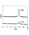
- FIG. 16 is a second view of the example of the manufacturing steps of the strain gauge of the first embodiment of the present invention; It is a figure which shows the result of the fluorescent-X-ray analysis of a functional layer. It is a figure which shows the result of X-ray diffraction of a resistor.
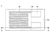
- FIG. 1 is a plan view illustrating a strain gauge according to a first embodiment.
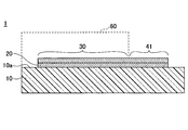
- FIG. 2 is a cross-sectional view illustrating the strain gauge according to the first embodiment, and shows a cross-section along the line AA of FIG.
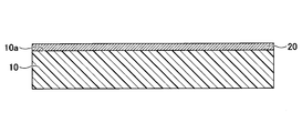
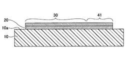
- the strain gauge 1 includes a base 10, a functional layer 20, a resistor 30, and a terminal portion 41.
- the side of the base material 10 on which the resistor 30 is provided is the upper side or one side, and the side on which the resistor 30 is not provided is the lower side or the other side.
- the surface on the side where the resistor 30 of each part is provided is referred to as one surface or upper surface, and the surface on the side where the resistor 30 is not provided is referred to as the other surface or lower surface.
- the strain gauge 1 can be used in the upside-down state or can be disposed at any angle.
- planar view refers to viewing the object in the normal direction of the upper surface 10a of the base material
- planar shape refers to a shape of the object viewed in the normal direction of the upper surface 10a of the base 10 I assume.
- the base 10 is a member to be a base layer for forming the resistor 30 and the like, and has flexibility.
- the thickness of the substrate 10 is not particularly limited and may be appropriately selected according to the purpose. For example, the thickness may be about 5 ⁇ m to 500 ⁇ m. In particular, when the thickness of the base material 10 is 5 ⁇ m to 200 ⁇ m, in terms of the transmission of strain from the surface of the strain-generating body joined to the lower surface of the base material 10 via the adhesive layer etc.
- the thickness is preferably 10 ⁇ m or more, further preferably in terms of insulation.
- the substrate 10 is made of, for example, PI (polyimide) resin, epoxy resin, PEEK (polyether ether ketone) resin, PEN (polyethylene naphthalate) resin, PET (polyethylene terephthalate) resin, PPS (polyphenylene sulfide) resin, polyolefin resin, etc.
- PI polyimide
- epoxy resin epoxy resin
- PEEK polyether ether ketone
- PEN polyethylene naphthalate
- PET polyethylene terephthalate
- PPS polyphenylene sulfide
- the substrate 10 may be formed of, for example, an insulating resin film containing a filler such as silica or alumina.
- the functional layer 20 is formed on the upper surface 10 a of the substrate 10 as a lower layer of the resistor 30. That is, the planar shape of the functional layer 20 is substantially the same as the planar shape of the resistor 30 shown in FIG.
- the thickness of the functional layer 20 can be, for example, about 1 nm to 100 nm.
- the functional layer refers to a layer having a function of promoting crystal growth of the resistor 30 which is at least the upper layer.
- the functional layer 20 preferably further has a function of preventing oxidation of the resistor 30 due to oxygen and moisture contained in the substrate 10, and a function of improving the adhesion between the substrate 10 and the resistor 30.
- the functional layer 20 may further have other functions.
- the insulating resin film constituting the substrate 10 contains oxygen and moisture, in particular when the resistor 30 contains Cr (chromium), the Cr forms a self-oxidized film, so the functional layer 20 oxidizes the resistor 30. It is effective to provide the function to prevent.
- the material of the functional layer 20 is not particularly limited as long as it has a function of promoting crystal growth of the resistor 30 which is at least the upper layer, and can be appropriately selected according to the purpose.
- Cr chromium
- Ti Ti
- V vanadium
- Nb niobium
- Ta tantalum
- Ni nickel
- Y yttrium
- Zr zirconium
- Hf hafnium
- Si silicon
- C carbon
- Cu copper
- Bi bismuth
- Fe iron
- Mo mobdenum
- W tungsten
- Ru ruthenium
- Rh Rhodium
- Re rhenium
- Os osmium
- Ir Iridium
- Pt platinum
- Pd palladium
- Ag silver
- Au gold
- Co cobalt
- Mn manganese
- Al aluminum
- One or more metals is-option, either metal alloys of this group, or
- FeCr, TiAl, FeNi, NiCr, CrCu etc. are mentioned, for example.
- As the above-mentioned compounds e.g., TiN, TaN, Si 3 N 4, TiO 2, Ta 2 O 5, SiO 2 , and the like.
- the resistor 30 is a thin film formed in a predetermined pattern on the upper surface of the functional layer 20, and is a sensing unit that receives strain and causes a change in resistance. In FIG. 1, for the sake of convenience, the resistor 30 is shown in a satin pattern.
- the resistor 30 can be formed of, for example, a material containing Cr (chromium), a material containing Ni (nickel), or a material containing both Cr and Ni. That is, the resistor 30 can be formed of a material containing at least one of Cr and Ni.
- a material containing Cr for example, a Cr multiphase film can be mentioned.
- a material containing Ni for example, Cu—Ni (copper nickel) can be mentioned.
- Ni-Cr nickel chromium
- the Cr multiphase film is a film in which Cr, CrN, Cr 2 N, etc. are mixed in phase.
- the Cr mixed phase film may contain unavoidable impurities such as chromium oxide.
- a part of the material constituting the functional layer 20 may be diffused into the Cr mixed phase film.
- the material constituting the functional layer 20 and nitrogen may form a compound.
- the Cr mixed phase film may contain Ti or TiN (titanium nitride).
- the thickness of the resistor 30 is not particularly limited and can be appropriately selected according to the purpose.
- the thickness can be set to about 0.05 ⁇ m to 2 ⁇ m.
- the thickness of the resistor 30 is 0.1 ⁇ m or more in that the crystallinity (for example, the crystallinity of ⁇ -Cr) of the crystals constituting the resistor 30 is improved, and the resistor of 1 ⁇ m or less It is further preferable in that it is possible to reduce the cracks of the film resulting from the internal stress of the film constituting 30 and the warpage from the base material 10.
- the resistor 30 By forming the resistor 30 on the functional layer 20, the resistor 30 can be formed with a stable crystal phase, so the stability of the gauge characteristics (gauge factor, gauge factor temperature coefficient TCS, and resistance temperature coefficient TCR) is improved. can do.
- the resistor 30 when the resistor 30 is a Cr mixed phase film, by providing the functional layer 20, the resistor 30 mainly composed of ⁇ -Cr (alpha chromium) can be formed. Since ⁇ -Cr is a stable crystal phase, the stability of the gauge characteristics can be improved.
- the main component means that the target substance occupies 50% by mass or more of all the substances constituting the resistor.
- the resistor 30 preferably contains 80% by weight or more of ⁇ -Cr from the viewpoint of improving the gauge characteristics.
- ⁇ -Cr is Cr of the bcc structure (body-centered cubic lattice structure).
- the metal (for example, Ti) constituting the functional layer 20 diffuses into the Cr mixed phase film, whereby the gauge characteristics can be improved.
- the gauge factor of the strain gauge 1 can be 10 or more, and the gauge factor temperature coefficient TCS and the resistance temperature coefficient TCR can be in the range of -1000 ppm / ° C to +1000 ppm / ° C.
- the terminal portion 41 extends from both ends of the resistor 30, and is wider than the resistor 30 and formed in a substantially rectangular shape in a plan view.
- the terminal portions 41 are a pair of electrodes for outputting a change in the resistance value of the resistor 30 caused by strain to the outside, and for example, a lead wire for external connection is joined.
- the resistor 30 extends, for example, from one of the terminal portions 41 in a zigzag manner and is connected to the other terminal portion 41.
- the upper surface of the terminal portion 41 may be coated with a metal having a better solderability than the terminal portion 41.
- the resistor 30 and the terminal part 41 are made into another code
- a cover layer 60 (insulating resin layer) may be provided on the upper surface 10 a of the base 10 so as to cover the resistor 30 and expose the terminal portion 41.
- the cover layer 60 may be provided so as to cover the entire portion excluding the terminal portion 41.
- the cover layer 60 can be formed of, for example, an insulating resin such as PI resin, epoxy resin, PEEK resin, PEN resin, PET resin, PPS resin, composite resin (for example, silicone resin, polyolefin resin).
- the cover layer 60 may contain a filler or a pigment.
- the thickness of the cover layer 60 is not particularly limited and may be appropriately selected depending on the purpose. For example, the thickness may be about 2 ⁇ m to 30 ⁇ m.
- FIGS. 3A and 3B are views illustrating the manufacturing process of the strain gauge according to the first embodiment, and show a cross section corresponding to FIG.
- the base material 10 is prepared, and the functional layer 20 is formed on the upper surface 10 a of the base material 10.
- the materials and thicknesses of the base 10 and the functional layer 20 are as described above.
- the functional layer 20 can be vacuum deposited, for example, by a conventional sputtering method in which Ar (argon) gas is introduced into the chamber with a source capable of forming the functional layer 20 as a target.
- Ar argon
- the functional layer 20 is formed while etching the upper surface 10 a of the substrate 10 with Ar, so that the amount of forming the functional layer 20 can be minimized to obtain the adhesion improvement effect. it can.
- the functional layer 20 may be formed by another method.
- the adhesion improvement effect is obtained by activating the upper surface 10a of the substrate 10 by plasma treatment using Ar or the like before film formation of the functional layer 20, and then the functional layer 20 is vacuum-deposited by magnetron sputtering.
- a method of film formation may be used.
- the functional layer 20 and the resistor 30 and the terminal portion 41 are formed into the planar shape shown in FIG. Pattern it.
- the materials and thicknesses of the resistor 30 and the terminal portion 41 are as described above.
- the resistor 30 and the terminal portion 41 can be integrally formed of the same material.
- the resistor 30 and the terminal portion 41 can be formed, for example, by a magnetron sputtering method using a raw material capable of forming the resistor 30 and the terminal portion 41 as a target.
- the resistor 30 and the terminal portion 41 may be formed by reactive sputtering, evaporation, arc ion plating, pulsed laser deposition, or the like, instead of the magnetron sputtering.
- the combination of the material of the functional layer 20 and the material of the resistor 30 and the terminal portion 41 is not particularly limited and may be appropriately selected according to the purpose.
- Ti is used as the functional layer 20, and the resistor 30 and the terminal portion It is possible to form a Cr mixed phase film containing ⁇ -Cr (alpha chromium) as a main component as 41.
- the resistor 30 and the terminal portion 41 can be formed by a magnetron sputtering method in which Ar gas is introduced into the chamber with a raw material capable of forming a Cr mixed phase film as a target.
- Ar gas is introduced into the chamber with a raw material capable of forming a Cr mixed phase film as a target.
- pure Cr may be used as a target
- an appropriate amount of nitrogen gas may be introduced into the chamber together with Ar gas, and the resistor 30 and the terminal portion 41 may be formed by reactive sputtering.
- the growth surface of the Cr multi-phase film is defined by the functional layer 20 made of Ti as a trigger, and a Cr multi-phase film mainly composed of ⁇ -Cr having a stable crystal structure can be formed. Further, the diffusion of Ti constituting the functional layer 20 into the Cr multiphase film improves the gauge characteristics.
- the gauge factor of the strain gauge 1 can be 10 or more, and the gauge factor temperature coefficient TCS and the resistance temperature coefficient TCR can be in the range of -1000 ppm / ° C to +1000 ppm / ° C.
- the functional layer 20 made of Ti has a function of promoting crystal growth of the resistor 30, and prevents the oxidation of the resistor 30 due to oxygen and moisture contained in the base material 10. All of the functions and functions to improve the adhesion between the substrate 10 and the resistor 30 are provided. The same applies to the case where Ta, Si, Al, or Fe is used as the functional layer 20 instead of Ti.
- the strain gauge 1 is completed by providing a cover layer 60 which covers the resistor 30 and exposes the terminal portion 41 on the upper surface 10a of the base 10, if necessary.
- the cover layer 60 is formed, for example, by laminating a thermosetting insulating resin film in a semi-hardened state on the upper surface 10 a of the base 10 so as to cover the resistor 30 and expose the terminal portion 41 and heat and cure it. It can be made.
- the cover layer 60 is formed by applying a liquid or paste-like thermosetting insulating resin on the upper surface 10 a of the base 10 so as to cover the resistor 30 and expose the terminal portion 41, and heat and cure it. May be
- the functional layer 20 in the lower layer of the resistor 30, it is possible to promote crystal growth of the resistor 30, and the resistor 30 composed of a stable crystal phase can be manufactured. As a result, in the strain gauge 1, the stability of the gauge characteristics can be improved. Further, the material constituting the functional layer 20 diffuses into the resistor 30, whereby the gauge characteristics of the strain gauge 1 can be improved.
- Example 1 First, as a preliminary experiment, Ti was vacuum-deposited as the functional layer 20 on the upper surface 10a of the substrate 10 made of polyimide resin with a thickness of 25 ⁇ m by conventional sputtering. Under the present circumstances, five samples which formed Ti film-forming aiming at several film thickness were produced.
- XRF fluorescent X-ray
- Example 1 Ti with a film thickness of 3 nm was vacuum-deposited as a functional layer 20 on the upper surface 10a of the substrate 10 made of polyimide resin with a thickness of 25 ⁇ m by conventional sputtering.
- the functional layer 20 and the resistor 30 and the terminal portion 41 are photolithographically as shown in FIG. Patterned.
- a Cr multiphase film is formed as the resistor 30 and the terminal portion 41 by the magnetron sputtering method without forming the functional layer 20 on the upper surface 10a of the substrate 10 made of polyimide resin with a thickness of 25 ⁇ m. And patterned as in FIG. 1 by photolithography.
- the film forming conditions of the resistor 30 and the terminal portion 41 are all the same.
- FIG. 5 is an X-ray diffraction pattern in a diffraction angle of 2 ⁇ of 36 to 48 degrees, and the diffraction peak of Example 1 is shifted to the right of the diffraction peak of Comparative Example 1. Moreover, the diffraction peak of Example 1 is higher than the diffraction peak of Comparative Example 1.
- Example 1 The diffraction peak of Example 1 is located in the vicinity of the diffraction line of ⁇ -Cr (110), and by providing the functional layer 20 made of Ti, the crystal growth of ⁇ -Cr is promoted to become ⁇ -Cr. It is considered that a Cr multi-phase film containing as a main component is formed.
- Example 1 a plurality of samples of Example 1 and a sample of Comparative Example 1 were produced, and gauge characteristics were measured. As a result, the gauge factor of each sample of Example 1 was 14 to 16, while the gauge factor of each sample of Comparative Example 1 was less than 10.
- the gauge temperature coefficient TCS and the resistance temperature coefficient TCR of each sample of Example 1 were within the range of -1000 ppm / ° C to +1000 ppm / ° C
- the gauge temperature coefficient TCS of each sample of Comparative Example 1 was And, the temperature coefficient of resistance TCR did not fall within the range of -1000 ppm / ° C to +1000 ppm / ° C.
- the functional layer 20 made of Ti crystal growth of ⁇ -Cr is promoted to form a Cr multi-phase film mainly composed of ⁇ -Cr, and the gauge factor is 10 or more, and the gauge factor A strain gauge having a temperature coefficient TCS and a temperature coefficient of resistance TCR of -1000 ppm / ° C. to +1000 ppm / ° C. was produced. It is considered that the diffusion effect of Ti to the Cr mixed phase film contributes to the improvement of the gauge characteristics.
Landscapes
- Chemical & Material Sciences (AREA)
- Chemical Kinetics & Catalysis (AREA)
- Engineering & Computer Science (AREA)
- Materials Engineering (AREA)
- Mechanical Engineering (AREA)
- Metallurgy (AREA)
- Organic Chemistry (AREA)
- Physics & Mathematics (AREA)
- General Physics & Mathematics (AREA)
- Measurement Of Length, Angles, Or The Like Using Electric Or Magnetic Means (AREA)
Priority Applications (6)
| Application Number | Priority Date | Filing Date | Title |
|---|---|---|---|
| CN202310346190.1A CN116608762B (zh) | 2017-09-29 | 2018-09-26 | 应变片 |
| CN201880076750.3A CN111417829B (zh) | 2017-09-29 | 2018-09-26 | 应变片 |
| US16/650,560 US11542590B2 (en) | 2017-09-29 | 2018-09-26 | Strain gauge |
| EP23187300.1A EP4269936B1 (en) | 2017-09-29 | 2018-09-26 | Strain gauge |
| EP18862478.7A EP3690387B1 (en) | 2017-09-29 | 2018-09-26 | Strain gauge |
| US17/929,830 US11702730B2 (en) | 2017-09-29 | 2022-09-06 | Strain gauge |
Applications Claiming Priority (2)
| Application Number | Priority Date | Filing Date | Title |
|---|---|---|---|
| JP2017191820A JP6793103B2 (ja) | 2017-09-29 | 2017-09-29 | ひずみゲージ |
| JP2017-191820 | 2017-09-29 |
Related Child Applications (2)
| Application Number | Title | Priority Date | Filing Date |
|---|---|---|---|
| US16/650,560 A-371-Of-International US11542590B2 (en) | 2017-09-29 | 2018-09-26 | Strain gauge |
| US17/929,830 Continuation US11702730B2 (en) | 2017-09-29 | 2022-09-06 | Strain gauge |
Publications (1)
| Publication Number | Publication Date |
|---|---|
| WO2019065740A1 true WO2019065740A1 (ja) | 2019-04-04 |
Family
ID=65901960
Family Applications (1)
| Application Number | Title | Priority Date | Filing Date |
|---|---|---|---|
| PCT/JP2018/035706 Ceased WO2019065740A1 (ja) | 2017-09-29 | 2018-09-26 | ひずみゲージ |
Country Status (5)
| Country | Link |
|---|---|
| US (2) | US11542590B2 (enExample) |
| EP (2) | EP3690387B1 (enExample) |
| JP (1) | JP6793103B2 (enExample) |
| CN (2) | CN116608762B (enExample) |
| WO (1) | WO2019065740A1 (enExample) |
Cited By (1)
| Publication number | Priority date | Publication date | Assignee | Title |
|---|---|---|---|---|
| WO2022092033A1 (ja) * | 2020-10-30 | 2022-05-05 | 日東電工株式会社 | 歪センサ、機能性フィルムおよびその製造方法 |
Families Citing this family (13)
| Publication number | Priority date | Publication date | Assignee | Title |
|---|---|---|---|---|
| JP7201542B2 (ja) * | 2019-06-21 | 2023-01-10 | ミネベアミツミ株式会社 | 転がり軸受、回転装置、軸受監視装置、軸受監視方法 |
| JP7390139B2 (ja) | 2019-09-05 | 2023-12-01 | ミネベアミツミ株式会社 | センサモジュール、ひずみ検出装置 |
| JP7426794B2 (ja) * | 2019-10-01 | 2024-02-02 | ミネベアミツミ株式会社 | センサモジュール |
| JP2021110703A (ja) * | 2020-01-15 | 2021-08-02 | ミネベアミツミ株式会社 | ひずみゲージ |
| JP7406517B2 (ja) * | 2020-03-24 | 2023-12-27 | ミネベアミツミ株式会社 | ひずみゲージ |
| JP7659380B2 (ja) * | 2020-10-30 | 2025-04-09 | 日東電工株式会社 | 積層フィルムおよび歪みセンサの製造方法 |
| JP7638081B2 (ja) * | 2020-10-30 | 2025-03-03 | 日東電工株式会社 | 積層フィルムおよび歪みセンサ |
| JP7736429B2 (ja) * | 2020-10-30 | 2025-09-09 | 日東電工株式会社 | 積層フィルム、第2積層フィルムの製造方法およびひずみセンサの製造方法 |
| JP2022106507A (ja) * | 2021-01-07 | 2022-07-20 | ミネベアミツミ株式会社 | ひずみゲージ |
| JP7189240B2 (ja) * | 2021-01-18 | 2022-12-13 | ミネベアミツミ株式会社 | ひずみゲージ |
| JP2023021714A (ja) * | 2021-08-02 | 2023-02-14 | ミネベアミツミ株式会社 | 脈波測定装置 |
| JP2023021715A (ja) * | 2021-08-02 | 2023-02-14 | ミネベアミツミ株式会社 | 脈波測定装置 |
| DE102021209525A1 (de) | 2021-08-31 | 2023-03-02 | CEROBEAR GmbH | Wälzlager und Verfahren zur Überwachung eines Wälzlagers |
Citations (10)
| Publication number | Priority date | Publication date | Assignee | Title |
|---|---|---|---|---|
| JPS5897607A (ja) * | 1981-12-07 | 1983-06-10 | Kyowa Dengiyou:Kk | ひずみゲ−ジ |
| JPH06300649A (ja) * | 1993-04-12 | 1994-10-28 | Sumitomo Electric Ind Ltd | 薄膜歪抵抗材料とその製造方法及び薄膜歪みセンサ |
| JPH08102163A (ja) * | 1994-09-30 | 1996-04-16 | Fujitsu Ltd | 磁気記録媒体及び磁気ディスク装置 |
| JPH0916941A (ja) * | 1995-01-31 | 1997-01-17 | Hoya Corp | 磁気記録媒体及びその製造方法 |
| US20050188769A1 (en) * | 2004-02-17 | 2005-09-01 | Thomas Moelkner | Micromechanical high-pressure sensor |
| JP2007173544A (ja) * | 2005-12-22 | 2007-07-05 | Toshiba Corp | X線検出器およびその製造方法 |
| JP2015031633A (ja) * | 2013-08-05 | 2015-02-16 | 公益財団法人電磁材料研究所 | 歪センサ |
| JP2016074934A (ja) | 2014-10-03 | 2016-05-12 | 株式会社東京測器研究所 | ひずみゲージ用合金及びひずみゲージ |
| JP2016136605A (ja) * | 2015-01-23 | 2016-07-28 | 株式会社豊田中央研究所 | 永久磁石およびその製造方法 |
| JP2017191820A (ja) | 2016-04-11 | 2017-10-19 | 株式会社デンソー | 半導体モジュール |
Family Cites Families (115)
| Publication number | Priority date | Publication date | Assignee | Title |
|---|---|---|---|---|
| US3867231A (en) | 1972-06-28 | 1975-02-18 | Goodyear Tire & Rubber | Tire building machine |
| JPS58169150A (ja) | 1982-03-30 | 1983-10-05 | Fujitsu Ltd | フオトマスクの製造方法 |
| JPS59164214A (ja) | 1983-03-09 | 1984-09-17 | Nissan Motor Co Ltd | 車両用サスペンシヨン装置 |
| JPS6058578U (ja) | 1983-09-30 | 1985-04-23 | 日産自動車株式会社 | 制動状態検出装置 |
| JPS60104554U (ja) | 1983-12-22 | 1985-07-17 | アルパイン株式会社 | ドアのロツク解除装置 |
| DE3403042A1 (de) * | 1984-01-30 | 1985-08-01 | Philips Patentverwaltung Gmbh, 2000 Hamburg | Duennfilm-dehnungsmessstreifen-system und verfahren zu seiner herstellung |
| US4658233A (en) | 1984-03-16 | 1987-04-14 | Fuji Electric Corporate Research & Development Ltd. | Strain gauge |
| DE3429649A1 (de) | 1984-08-11 | 1986-02-20 | Vdo Adolf Schindling Ag, 6000 Frankfurt | Elektrischer widerstand |
| JPS61176803A (ja) * | 1985-01-31 | 1986-08-08 | Hitachi Ltd | ストレインゲージ |
| JPS61288401A (ja) | 1985-06-14 | 1986-12-18 | 株式会社村田製作所 | 薄膜抵抗体 |
| JPS63165725A (ja) | 1986-12-26 | 1988-07-09 | Aisin Seiki Co Ltd | 圧力センサ−用歪ゲ−ジ |
| JP2516964B2 (ja) | 1987-03-31 | 1996-07-24 | 鐘淵化学工業株式会社 | 歪センサ− |
| US4937550A (en) | 1987-03-31 | 1990-06-26 | Kanegafuchi Kagaku Kogyo Kabushiki Kaisha | Strain sensor |
| JPH0731091B2 (ja) | 1987-05-27 | 1995-04-10 | 日本碍子株式会社 | 歪検出器 |
| JP2585681B2 (ja) | 1988-02-08 | 1997-02-26 | 株式会社タイセー | 金属薄膜抵抗ひずみゲ―ジ |
| JPH02117476A (ja) | 1988-10-25 | 1990-05-01 | Daikyo Webasto Co Ltd | 車輌の可動式リヤスポイラー |
| JPH02189981A (ja) | 1989-01-19 | 1990-07-25 | Ricoh Co Ltd | 半導体装置及びその製造法 |
| US5154247A (en) | 1989-10-31 | 1992-10-13 | Teraoka Seiko Co., Limited | Load cell |
| JPH0495738A (ja) | 1990-08-06 | 1992-03-27 | Teraoka Seiko Co Ltd | ロードセル |
| JPH03191802A (ja) | 1989-12-21 | 1991-08-21 | Sumitomo Electric Ind Ltd | 感歪素子 |
| JP2890601B2 (ja) * | 1990-02-08 | 1999-05-17 | 株式会社デンソー | 半導体センサ |
| US5349746A (en) | 1990-05-07 | 1994-09-27 | Robert Bosch Gmbh | Process for the manufacture of a force sensor |
| JPH0438402A (ja) | 1990-06-02 | 1992-02-07 | Kyowa Electron Instr Co Ltd | ひずみゲージとその製造方法 |
| DE59006630D1 (de) | 1990-06-05 | 1994-09-01 | Hottinger Messtechnik Baldwin | Dehnungsmessstreifen. |
| JPH05308107A (ja) | 1991-07-01 | 1993-11-19 | Sumitomo Electric Ind Ltd | 半導体装置及びその製作方法 |
| JPH0580070A (ja) | 1991-09-24 | 1993-03-30 | Aisin Seiki Co Ltd | 歪ゲージ素子及びその製造方法 |
| JPH05145142A (ja) | 1991-11-19 | 1993-06-11 | Matsushita Electric Ind Co Ltd | 磁気抵抗素子 |
| JPH0640305A (ja) | 1992-07-23 | 1994-02-15 | Toyota Motor Corp | エアバッグの圧力調整装置 |
| US5328551A (en) | 1992-10-28 | 1994-07-12 | Eaton Corporation | Method of making high output strain gage |
| JPH06176903A (ja) | 1992-12-03 | 1994-06-24 | Nippon Soken Inc | Cr系サーメット薄膜の電極構造 |
| JPH07113697A (ja) | 1993-10-19 | 1995-05-02 | Tec Corp | ロードセル |
| JP3233248B2 (ja) | 1994-05-13 | 2001-11-26 | エヌオーケー株式会社 | 歪ゲ−ジ用薄膜およびその製造法 |
| JPH08304200A (ja) | 1995-05-09 | 1996-11-22 | Matsushita Electric Ind Co Ltd | 感歪み抵抗体ペーストおよびこれを用いた力学量センサ |
| JPH09197435A (ja) | 1996-01-17 | 1997-07-31 | Toshiba Corp | 液晶表示装置、及びその製造方法 |
| JP3642449B2 (ja) * | 1997-03-21 | 2005-04-27 | 財団法人電気磁気材料研究所 | Cr−N基歪抵抗膜およびその製造法ならびに歪センサ |
| JP2000146511A (ja) | 1998-11-06 | 2000-05-26 | Mitsubishi Heavy Ind Ltd | 歪ゲージ |
| JP2000207102A (ja) * | 1999-01-18 | 2000-07-28 | Alps Electric Co Ltd | キ―ボ―ド装置 |
| DE60025355T2 (de) | 1999-07-09 | 2006-08-17 | Nok Corp. | Dehnungsmessstreifen |
| JP2002221453A (ja) | 2001-01-29 | 2002-08-09 | Nippon Denshi Kogyo Kk | 構造体の荷重情報収集装置 |
| JP4482250B2 (ja) | 2001-07-19 | 2010-06-16 | 本田技研工業株式会社 | 圧力感度及び温度感度を低減したひずみゲージ及びその設計方法 |
| US20030016116A1 (en) | 2001-07-23 | 2003-01-23 | Blaha Charles A. | Method of depositing a thin metallic film and related apparatus |
| JP2003097906A (ja) | 2001-09-27 | 2003-04-03 | Tokyo Sokki Kenkyusho Co Ltd | ひずみゲージ及びひずみ測定方法 |
| JP2003324258A (ja) | 2002-05-01 | 2003-11-14 | Nippon Mektron Ltd | プリント配線板用銅張板 |
| US7276994B2 (en) * | 2002-05-23 | 2007-10-02 | Murata Manufacturing Co., Ltd. | Piezoelectric thin-film resonator, piezoelectric filter, and electronic component including the piezoelectric filter |
| JP2004072715A (ja) | 2002-06-11 | 2004-03-04 | Murata Mfg Co Ltd | 圧電薄膜共振子、圧電フィルタ、およびそれを有する電子部品 |
| CN1300806C (zh) | 2002-06-06 | 2007-02-14 | 阿尔卑斯电气株式会社 | 电阻元件及其制造方法 |
| US7106167B2 (en) | 2002-06-28 | 2006-09-12 | Heetronix | Stable high temperature sensor system with tungsten on AlN |
| AU2003254888A1 (en) * | 2002-08-08 | 2004-02-25 | Kabushiki Kaisha Kobe Seiko Sho | PROCESS FOR PRODUCING ALUMINA COATING COMPOSED MAINLY OF Alpha-TYPE CRYSTAL STRUCTURE, ALUMINA COATING COMPOSED MAINLY OF Alpha-TYPE CRYSTAL STRUCTURE, LAMINATE COATING INCLUDING THE ALUMINA COATING, MEMBER CLAD WITH THE ALUMINA COATING OR LAMINATE COATING, PROCESS FOR PRODUCING THE MEMBER, AND PHYSICAL EVAPORATION APPARATU |
| TW552406B (en) * | 2003-01-30 | 2003-09-11 | Microcosm Technology Co Ltd | Manufacturing method of strain transducer substrate and the product thereof |
| US20040159162A1 (en) | 2003-02-19 | 2004-08-19 | Vishay Intertechnology | Strain gage |
| JP2005132216A (ja) | 2003-10-30 | 2005-05-26 | Matsushita Electric Ind Co Ltd | 踏力センサとそれを用いたペダル踏力検出装置 |
| ATE441843T1 (de) | 2004-01-27 | 2009-09-15 | Mettler Toledo Ag | Kraftmesszelle mit dehnmessstreifen mit klebeschicht aus anorganisch-organischem hybrid- polymer (ormocer) |
| JP2006118982A (ja) | 2004-10-21 | 2006-05-11 | Denso Corp | 車両用前方衝突荷重検出装置 |
| JP4742577B2 (ja) | 2004-12-14 | 2011-08-10 | 日産自動車株式会社 | 圧力センサおよびその製造方法 |
| EP1934668B1 (en) | 2005-09-06 | 2016-03-16 | Beyond Blades Ltd. | 3-dimensional multi-layered modular computer architecture |
| JP4814594B2 (ja) | 2005-09-14 | 2011-11-16 | 日立オートモティブシステムズ株式会社 | 車載設備の操作装置 |
| JP4909583B2 (ja) | 2005-12-16 | 2012-04-04 | 株式会社昭和測器 | 多軸力ロードセル |
| EP2080685B1 (de) | 2008-01-16 | 2011-04-27 | Ford Global Technologies, LLC | Drehmomentsensierung mittels integrierter Dehnungsmessstreifen |
| JP2010070850A (ja) | 2008-08-21 | 2010-04-02 | Mitsubishi Materials Corp | 銅張積層板およびその製造方法並びにプリント配線板およびその製造方法 |
| JP5279426B2 (ja) | 2008-09-19 | 2013-09-04 | ミサワホーム株式会社 | ドアロックシステム |
| JP2011103327A (ja) | 2009-11-10 | 2011-05-26 | Seiko Epson Corp | 圧電素子、圧電アクチュエーター、液体噴射ヘッドおよび液体噴射装置 |
| JP2011240794A (ja) | 2010-05-18 | 2011-12-01 | Takashi Aono | 車両認識音発生装置 |
| WO2011156447A1 (en) | 2010-06-11 | 2011-12-15 | 3M Innovative Properties Company | Positional touch sensor with force measurement |
| US8232026B2 (en) | 2010-10-14 | 2012-07-31 | Ford Global Technologies, Llc | Bipolar plates for electrochemical cells |
| JP2012151338A (ja) | 2011-01-20 | 2012-08-09 | Elpida Memory Inc | 半導体装置の製造方法及びハードマスクの形成方法 |
| JP5884110B2 (ja) | 2011-12-02 | 2016-03-15 | 株式会社アサヒ電子研究所 | 歪抵抗素子およびそれを用いた歪検出装置 |
| TWI476969B (zh) | 2012-01-13 | 2015-03-11 | Univ Nat Kaohsiung Applied Sci | Metal silicide thermal sensor and its preparation method |
| JP5539430B2 (ja) | 2012-03-22 | 2014-07-02 | 富士フイルム株式会社 | 電子機器の製造方法 |
| JP2013217763A (ja) * | 2012-04-09 | 2013-10-24 | Honda Motor Co Ltd | 薄膜ひずみセンサ用材料およびこれを用いた薄膜ひずみセンサ |
| JP5670502B2 (ja) | 2012-04-30 | 2015-02-18 | 株式会社エスアンドエス テック | 位相反転ブランクマスク及びその製造方法 |
| US20150276517A1 (en) | 2012-05-25 | 2015-10-01 | Hitachi, Ltd. | Mechanical Quantity Measuring Device |
| CN103580980B (zh) | 2012-07-24 | 2019-05-24 | 中兴通讯股份有限公司 | 虚拟网络自动发现和自动配置的方法及其装置 |
| JP6084393B2 (ja) | 2012-08-08 | 2017-02-22 | 公益財団法人電磁材料研究所 | 歪センサおよび歪の測定方法 |
| JP6022881B2 (ja) | 2012-10-04 | 2016-11-09 | 公益財団法人電磁材料研究所 | 歪ゲージ |
| US9306207B2 (en) | 2012-12-28 | 2016-04-05 | Hyundai Motor Company | Method of fabricating sulfur-infiltrated mesoporous conductive nanocomposites for cathode of lithium-sulfur secondary battery |
| JP6075114B2 (ja) | 2013-02-27 | 2017-02-08 | ローム株式会社 | 半導体装置および半導体装置の製造方法 |
| US9469107B2 (en) | 2013-07-12 | 2016-10-18 | Hewlett-Packard Development Company, L.P. | Thermal inkjet printhead stack with amorphous metal resistor |
| US20150296607A1 (en) | 2014-04-11 | 2015-10-15 | Apple Inc. | Electronic Device With Flexible Printed Circuit Strain Gauge Sensor |
| EP3153833B1 (en) | 2014-06-09 | 2020-10-21 | Hitachi Automotive Systems, Ltd. | Dynamic quantity measuring device and pressure sensor using same |
| JP6276658B2 (ja) | 2014-07-09 | 2018-02-07 | 新光電気工業株式会社 | 膜厚測定機能付き基板及び絶縁層の膜厚測定方法 |
| CA3006938C (en) | 2014-12-10 | 2023-08-15 | Paul D. Okulov | Micro electro-mechanical strain displacement sensor and usage monitoring system |
| JP6411916B2 (ja) | 2015-02-26 | 2018-10-24 | ラピスセミコンダクタ株式会社 | 半導体装置、ワイパシステム、及び移動体制御方法 |
| US9714876B2 (en) * | 2015-03-26 | 2017-07-25 | Sensata Technologies, Inc. | Semiconductor strain gauge |
| US9933321B2 (en) * | 2015-05-14 | 2018-04-03 | Vishay Measurements Group, Inc. | High gage factor strain gage |
| JP6332303B2 (ja) | 2015-06-01 | 2018-05-30 | 日亜化学工業株式会社 | 金属被覆方法及び発光装置とその製造方法 |
| WO2016203354A1 (en) | 2015-06-19 | 2016-12-22 | Semiconductor Energy Laboratory Co., Ltd. | Semiconductor device, manufacturing method thereof, and electronic device |
| JP2017067764A (ja) | 2015-09-29 | 2017-04-06 | ミネベアミツミ株式会社 | ひずみゲージ、荷重センサ、及びひずみゲージの製造方法 |
| US10353503B2 (en) | 2015-10-29 | 2019-07-16 | Texas Instruments Incorporated | Integrated force sensing element |
| JP2017101983A (ja) | 2015-12-01 | 2017-06-08 | 日本写真印刷株式会社 | 多点計測用のひずみセンサとその製造方法 |
| JP6701748B2 (ja) | 2016-01-19 | 2020-05-27 | ヤマハ株式会社 | 歪みセンサ素子 |
| US10054503B2 (en) | 2016-03-11 | 2018-08-21 | Microsoft Technology Licensing, Llc | Force sensor |
| CN105755438B (zh) | 2016-03-30 | 2018-12-18 | 上海交通大学 | 一种高温自补偿多层复合薄膜应变计及其制备方法 |
| JP5988004B1 (ja) | 2016-04-12 | 2016-09-07 | Tdk株式会社 | 電子回路パッケージ |
| JP6607820B2 (ja) | 2016-04-12 | 2019-11-20 | 東京エレクトロン株式会社 | フィルタ立ち上げ装置、処理液供給装置、治具ユニット、フィルタの立ち上げ方法 |
| CN105908142B (zh) * | 2016-04-15 | 2018-08-14 | 大连交通大学 | 一种高温薄膜应变计及其制作方法 |
| DE102016108985A1 (de) * | 2016-05-13 | 2017-11-16 | Trafag Ag | Verfahren zur Herstellung eines Sensorelements mittels Laserstrukturierung |
| TWI581170B (zh) | 2016-05-19 | 2017-05-01 | 速博思股份有限公司 | 具金屬走線的壓力觸控裝置 |
| JP7223489B2 (ja) | 2016-05-27 | 2023-02-16 | デンカ株式会社 | 組成物 |
| JP2017210572A (ja) | 2016-05-27 | 2017-11-30 | 株式会社ファンケル | 抗酸化組成物 |
| JP2018048894A (ja) | 2016-09-21 | 2018-03-29 | 株式会社東芝 | センサ及び電子機器 |
| JP2018058549A (ja) | 2016-10-07 | 2018-04-12 | スズキ株式会社 | 車両用盗難防止装置 |
| CN106768524A (zh) | 2017-02-20 | 2017-05-31 | 广东海洋大学 | 一种薄膜压力传感器及其制造方法 |
| JP6762896B2 (ja) | 2017-03-22 | 2020-09-30 | アズビル株式会社 | 圧力センサチップ、圧力発信器、および圧力センサチップの製造方法 |
| JP2019066454A (ja) | 2017-09-29 | 2019-04-25 | ミネベアミツミ株式会社 | ひずみゲージ、センサモジュール |
| JP2019066312A (ja) | 2017-09-29 | 2019-04-25 | ミネベアミツミ株式会社 | ひずみゲージ |
| JP2019066453A (ja) | 2017-09-29 | 2019-04-25 | ミネベアミツミ株式会社 | ひずみゲージ |
| JP2019066313A (ja) | 2017-09-29 | 2019-04-25 | ミネベアミツミ株式会社 | ひずみゲージ |
| JP2019082424A (ja) * | 2017-10-31 | 2019-05-30 | ミネベアミツミ株式会社 | ひずみゲージ |
| JP2019090723A (ja) | 2017-11-15 | 2019-06-13 | ミネベアミツミ株式会社 | ひずみゲージ |
| JP2019113411A (ja) | 2017-12-22 | 2019-07-11 | ミネベアミツミ株式会社 | ひずみゲージ、センサモジュール |
| JP2019132790A (ja) | 2018-02-02 | 2019-08-08 | ミネベアミツミ株式会社 | ひずみゲージ |
| JP2018132531A (ja) | 2018-05-17 | 2018-08-23 | ミネベアミツミ株式会社 | ひずみゲージ |
| JP6660425B2 (ja) | 2018-07-20 | 2020-03-11 | ミネベアミツミ株式会社 | 姿勢制御装置 |
| JP7193262B2 (ja) | 2018-07-23 | 2022-12-20 | ミネベアミツミ株式会社 | 触覚センサ |
| US12159983B2 (en) | 2018-09-04 | 2024-12-03 | Hutchinson Technology Incorporated | Sensored battery pouch |
-
2017
- 2017-09-29 JP JP2017191820A patent/JP6793103B2/ja active Active
-
2018
- 2018-09-26 CN CN202310346190.1A patent/CN116608762B/zh active Active
- 2018-09-26 WO PCT/JP2018/035706 patent/WO2019065740A1/ja not_active Ceased
- 2018-09-26 CN CN201880076750.3A patent/CN111417829B/zh active Active
- 2018-09-26 EP EP18862478.7A patent/EP3690387B1/en active Active
- 2018-09-26 EP EP23187300.1A patent/EP4269936B1/en active Active
- 2018-09-26 US US16/650,560 patent/US11542590B2/en active Active
-
2022
- 2022-09-06 US US17/929,830 patent/US11702730B2/en active Active
Patent Citations (10)
| Publication number | Priority date | Publication date | Assignee | Title |
|---|---|---|---|---|
| JPS5897607A (ja) * | 1981-12-07 | 1983-06-10 | Kyowa Dengiyou:Kk | ひずみゲ−ジ |
| JPH06300649A (ja) * | 1993-04-12 | 1994-10-28 | Sumitomo Electric Ind Ltd | 薄膜歪抵抗材料とその製造方法及び薄膜歪みセンサ |
| JPH08102163A (ja) * | 1994-09-30 | 1996-04-16 | Fujitsu Ltd | 磁気記録媒体及び磁気ディスク装置 |
| JPH0916941A (ja) * | 1995-01-31 | 1997-01-17 | Hoya Corp | 磁気記録媒体及びその製造方法 |
| US20050188769A1 (en) * | 2004-02-17 | 2005-09-01 | Thomas Moelkner | Micromechanical high-pressure sensor |
| JP2007173544A (ja) * | 2005-12-22 | 2007-07-05 | Toshiba Corp | X線検出器およびその製造方法 |
| JP2015031633A (ja) * | 2013-08-05 | 2015-02-16 | 公益財団法人電磁材料研究所 | 歪センサ |
| JP2016074934A (ja) | 2014-10-03 | 2016-05-12 | 株式会社東京測器研究所 | ひずみゲージ用合金及びひずみゲージ |
| JP2016136605A (ja) * | 2015-01-23 | 2016-07-28 | 株式会社豊田中央研究所 | 永久磁石およびその製造方法 |
| JP2017191820A (ja) | 2016-04-11 | 2017-10-19 | 株式会社デンソー | 半導体モジュール |
Cited By (4)
| Publication number | Priority date | Publication date | Assignee | Title |
|---|---|---|---|---|
| WO2022092033A1 (ja) * | 2020-10-30 | 2022-05-05 | 日東電工株式会社 | 歪センサ、機能性フィルムおよびその製造方法 |
| JP2022072655A (ja) * | 2020-10-30 | 2022-05-17 | 日東電工株式会社 | 歪センサ、機能性フィルムおよびその製造方法 |
| US20240003762A1 (en) * | 2020-10-30 | 2024-01-04 | Nitto Denko Corporation | Strain sensor, functional film, and method for manufacturing same |
| JP7592461B2 (ja) | 2020-10-30 | 2024-12-02 | 日東電工株式会社 | 歪センサ、機能性フィルムおよびその製造方法 |
Also Published As
| Publication number | Publication date |
|---|---|
| JP2019066311A (ja) | 2019-04-25 |
| JP6793103B2 (ja) | 2020-12-02 |
| EP3690387A1 (en) | 2020-08-05 |
| CN111417829A (zh) | 2020-07-14 |
| US11702730B2 (en) | 2023-07-18 |
| US20200325571A1 (en) | 2020-10-15 |
| EP4269936B1 (en) | 2024-08-07 |
| CN116608762B (zh) | 2025-09-05 |
| CN111417829B (zh) | 2023-04-25 |
| EP4269936A3 (en) | 2023-12-13 |
| CN116608762A (zh) | 2023-08-18 |
| EP3690387A4 (en) | 2021-06-09 |
| EP3690387B1 (en) | 2023-11-01 |
| US11542590B2 (en) | 2023-01-03 |
| EP4269936A2 (en) | 2023-11-01 |
| US20220411915A1 (en) | 2022-12-29 |
Similar Documents
| Publication | Publication Date | Title |
|---|---|---|
| US11702730B2 (en) | Strain gauge | |
| JP7764650B2 (ja) | ひずみゲージ | |
| WO2019065744A1 (ja) | ひずみゲージ | |
| US11326966B2 (en) | Strain gauge with improved design to reduce pinholes and damage | |
| WO2019098048A1 (ja) | ひずみゲージ | |
| JP7659746B2 (ja) | ひずみゲージ | |
| JP2023118855A (ja) | ひずみゲージ | |
| JP2023126667A (ja) | ひずみゲージ | |
| JP2023105037A (ja) | ひずみゲージ | |
| WO2019098047A1 (ja) | ひずみゲージ | |
| WO2019098049A1 (ja) | ひずみゲージ | |
| JP2019100883A (ja) | ひずみゲージ | |
| WO2019088119A1 (ja) | ひずみゲージ | |
| WO2019088120A1 (ja) | ひずみゲージ | |
| JP2025115513A (ja) | ひずみゲージ |
Legal Events
| Date | Code | Title | Description |
|---|---|---|---|
| 121 | Ep: the epo has been informed by wipo that ep was designated in this application |
Ref document number: 18862478 Country of ref document: EP Kind code of ref document: A1 |
|
| DPE1 | Request for preliminary examination filed after expiration of 19th month from priority date (pct application filed from 20040101) | ||
| NENP | Non-entry into the national phase |
Ref country code: DE |
|
| ENP | Entry into the national phase |
Ref document number: 2018862478 Country of ref document: EP Effective date: 20200429 |