WO2019065740A1 - Strain gauge - Google Patents
Strain gauge Download PDFInfo
- Publication number
- WO2019065740A1 WO2019065740A1 PCT/JP2018/035706 JP2018035706W WO2019065740A1 WO 2019065740 A1 WO2019065740 A1 WO 2019065740A1 JP 2018035706 W JP2018035706 W JP 2018035706W WO 2019065740 A1 WO2019065740 A1 WO 2019065740A1
- Authority
- WO
- WIPO (PCT)
- Prior art keywords
- resistor
- functional layer
- strain gauge
- film
- gauge
- Prior art date
Links
- 239000011651 chromium Substances 0.000 claims abstract description 55
- 239000002346 layers by function Substances 0.000 claims abstract description 53
- 239000000463 material Substances 0.000 claims abstract description 35
- PXHVJJICTQNCMI-UHFFFAOYSA-N Nickel Chemical compound [Ni] PXHVJJICTQNCMI-UHFFFAOYSA-N 0.000 claims abstract description 21
- 239000000758 substrate Substances 0.000 claims abstract description 20
- 229910052804 chromium Inorganic materials 0.000 claims abstract description 14
- VYZAMTAEIAYCRO-UHFFFAOYSA-N Chromium Chemical compound [Cr] VYZAMTAEIAYCRO-UHFFFAOYSA-N 0.000 claims abstract description 11
- 229910052759 nickel Inorganic materials 0.000 claims abstract description 10
- 229910052751 metal Inorganic materials 0.000 claims abstract description 9
- 239000002184 metal Substances 0.000 claims abstract description 9
- 229910045601 alloy Inorganic materials 0.000 claims abstract description 4
- 239000000956 alloy Substances 0.000 claims abstract description 4
- 229920005989 resin Polymers 0.000 claims description 20
- 239000011347 resin Substances 0.000 claims description 20
- 239000010936 titanium Substances 0.000 claims description 20
- 239000010410 layer Substances 0.000 claims description 19
- 239000013078 crystal Substances 0.000 claims description 12
- NRTOMJZYCJJWKI-UHFFFAOYSA-N Titanium nitride Chemical compound [Ti]#N NRTOMJZYCJJWKI-UHFFFAOYSA-N 0.000 claims description 5
- 150000001875 compounds Chemical class 0.000 claims description 5
- 230000001737 promoting effect Effects 0.000 claims description 4
- RTAQQCXQSZGOHL-UHFFFAOYSA-N Titanium Chemical compound [Ti] RTAQQCXQSZGOHL-UHFFFAOYSA-N 0.000 claims description 3
- 229910052719 titanium Inorganic materials 0.000 claims description 3
- CXOWYMLTGOFURZ-UHFFFAOYSA-N azanylidynechromium Chemical compound [Cr]#N CXOWYMLTGOFURZ-UHFFFAOYSA-N 0.000 claims 1
- 150000002736 metal compounds Chemical class 0.000 abstract 1
- 239000010408 film Substances 0.000 description 37
- 238000000034 method Methods 0.000 description 11
- 230000000052 comparative effect Effects 0.000 description 8
- 238000001755 magnetron sputter deposition Methods 0.000 description 6
- 238000002441 X-ray diffraction Methods 0.000 description 5
- XEEYBQQBJWHFJM-UHFFFAOYSA-N iron Substances [Fe] XEEYBQQBJWHFJM-UHFFFAOYSA-N 0.000 description 4
- 238000004519 manufacturing process Methods 0.000 description 4
- -1 polyethylene naphthalate Polymers 0.000 description 4
- 229920001721 polyimide Polymers 0.000 description 4
- 230000008569 process Effects 0.000 description 4
- 238000004544 sputter deposition Methods 0.000 description 4
- IJGRMHOSHXDMSA-UHFFFAOYSA-N Atomic nitrogen Chemical compound N#N IJGRMHOSHXDMSA-UHFFFAOYSA-N 0.000 description 3
- 239000004696 Poly ether ether ketone Substances 0.000 description 3
- 239000004734 Polyphenylene sulfide Substances 0.000 description 3
- QVGXLLKOCUKJST-UHFFFAOYSA-N atomic oxygen Chemical compound [O] QVGXLLKOCUKJST-UHFFFAOYSA-N 0.000 description 3
- 230000000694 effects Effects 0.000 description 3
- 239000000945 filler Substances 0.000 description 3
- 239000007789 gas Substances 0.000 description 3
- 230000006872 improvement Effects 0.000 description 3
- 239000001301 oxygen Substances 0.000 description 3
- 229910052760 oxygen Inorganic materials 0.000 description 3
- KDLHZDBZIXYQEI-UHFFFAOYSA-N palladium Substances [Pd] KDLHZDBZIXYQEI-UHFFFAOYSA-N 0.000 description 3
- BASFCYQUMIYNBI-UHFFFAOYSA-N platinum Substances [Pt] BASFCYQUMIYNBI-UHFFFAOYSA-N 0.000 description 3
- 229920003207 poly(ethylene-2,6-naphthalate) Polymers 0.000 description 3
- 229920002530 polyetherether ketone Polymers 0.000 description 3
- 239000011112 polyethylene naphthalate Substances 0.000 description 3
- 239000005020 polyethylene terephthalate Substances 0.000 description 3
- 229920000139 polyethylene terephthalate Polymers 0.000 description 3
- 239000009719 polyimide resin Substances 0.000 description 3
- 229920000069 polyphenylene sulfide Polymers 0.000 description 3
- XKRFYHLGVUSROY-UHFFFAOYSA-N Argon Chemical compound [Ar] XKRFYHLGVUSROY-UHFFFAOYSA-N 0.000 description 2
- 229910018487 Ni—Cr Inorganic materials 0.000 description 2
- VYPSYNLAJGMNEJ-UHFFFAOYSA-N Silicium dioxide Chemical compound O=[Si]=O VYPSYNLAJGMNEJ-UHFFFAOYSA-N 0.000 description 2
- 229910052782 aluminium Inorganic materials 0.000 description 2
- 238000004458 analytical method Methods 0.000 description 2
- 230000015572 biosynthetic process Effects 0.000 description 2
- 230000008859 change Effects 0.000 description 2
- VNNRSPGTAMTISX-UHFFFAOYSA-N chromium nickel Chemical compound [Cr].[Ni] VNNRSPGTAMTISX-UHFFFAOYSA-N 0.000 description 2
- 239000010949 copper Substances 0.000 description 2
- 238000009792 diffusion process Methods 0.000 description 2
- 239000003822 epoxy resin Substances 0.000 description 2
- 239000010931 gold Substances 0.000 description 2
- 239000012535 impurity Substances 0.000 description 2
- 239000011572 manganese Substances 0.000 description 2
- 238000005259 measurement Methods 0.000 description 2
- 150000002739 metals Chemical class 0.000 description 2
- 239000010955 niobium Substances 0.000 description 2
- 230000003647 oxidation Effects 0.000 description 2
- 238000007254 oxidation reaction Methods 0.000 description 2
- 229920000647 polyepoxide Polymers 0.000 description 2
- 229920005672 polyolefin resin Polymers 0.000 description 2
- 239000002994 raw material Substances 0.000 description 2
- 238000005546 reactive sputtering Methods 0.000 description 2
- 239000010948 rhodium Substances 0.000 description 2
- 229910052710 silicon Inorganic materials 0.000 description 2
- 229910052715 tantalum Inorganic materials 0.000 description 2
- 229920001187 thermosetting polymer Polymers 0.000 description 2
- 239000011701 zinc Substances 0.000 description 2
- OKTJSMMVPCPJKN-UHFFFAOYSA-N Carbon Chemical compound [C] OKTJSMMVPCPJKN-UHFFFAOYSA-N 0.000 description 1
- RYGMFSIKBFXOCR-UHFFFAOYSA-N Copper Chemical compound [Cu] RYGMFSIKBFXOCR-UHFFFAOYSA-N 0.000 description 1
- 229910000570 Cupronickel Inorganic materials 0.000 description 1
- 229910002482 Cu–Ni Inorganic materials 0.000 description 1
- 229910002555 FeNi Inorganic materials 0.000 description 1
- 229910000604 Ferrochrome Inorganic materials 0.000 description 1
- PWHULOQIROXLJO-UHFFFAOYSA-N Manganese Chemical compound [Mn] PWHULOQIROXLJO-UHFFFAOYSA-N 0.000 description 1
- ZOKXTWBITQBERF-UHFFFAOYSA-N Molybdenum Chemical compound [Mo] ZOKXTWBITQBERF-UHFFFAOYSA-N 0.000 description 1
- KJTLSVCANCCWHF-UHFFFAOYSA-N Ruthenium Chemical compound [Ru] KJTLSVCANCCWHF-UHFFFAOYSA-N 0.000 description 1
- 229910004298 SiO 2 Inorganic materials 0.000 description 1
- 229910010038 TiAl Inorganic materials 0.000 description 1
- 229910010413 TiO 2 Inorganic materials 0.000 description 1
- WGLPBDUCMAPZCE-UHFFFAOYSA-N Trioxochromium Chemical compound O=[Cr](=O)=O WGLPBDUCMAPZCE-UHFFFAOYSA-N 0.000 description 1
- HCHKCACWOHOZIP-UHFFFAOYSA-N Zinc Chemical compound [Zn] HCHKCACWOHOZIP-UHFFFAOYSA-N 0.000 description 1
- QCWXUUIWCKQGHC-UHFFFAOYSA-N Zirconium Chemical compound [Zr] QCWXUUIWCKQGHC-UHFFFAOYSA-N 0.000 description 1
- 230000003213 activating effect Effects 0.000 description 1
- 239000012790 adhesive layer Substances 0.000 description 1
- XAGFODPZIPBFFR-UHFFFAOYSA-N aluminium Chemical compound [Al] XAGFODPZIPBFFR-UHFFFAOYSA-N 0.000 description 1
- PNEYBMLMFCGWSK-UHFFFAOYSA-N aluminium oxide Inorganic materials [O-2].[O-2].[O-2].[Al+3].[Al+3] PNEYBMLMFCGWSK-UHFFFAOYSA-N 0.000 description 1
- 229910052786 argon Inorganic materials 0.000 description 1
- 230000005540 biological transmission Effects 0.000 description 1
- 229910052797 bismuth Inorganic materials 0.000 description 1
- JCXGWMGPZLAOME-UHFFFAOYSA-N bismuth atom Chemical compound [Bi] JCXGWMGPZLAOME-UHFFFAOYSA-N 0.000 description 1
- 229910052799 carbon Inorganic materials 0.000 description 1
- 229910000423 chromium oxide Inorganic materials 0.000 description 1
- 229910017052 cobalt Inorganic materials 0.000 description 1
- 239000010941 cobalt Substances 0.000 description 1
- GUTLYIVDDKVIGB-UHFFFAOYSA-N cobalt atom Chemical compound [Co] GUTLYIVDDKVIGB-UHFFFAOYSA-N 0.000 description 1
- 239000000805 composite resin Substances 0.000 description 1
- 229910052802 copper Inorganic materials 0.000 description 1
- YOCUPQPZWBBYIX-UHFFFAOYSA-N copper nickel Chemical compound [Ni].[Cu] YOCUPQPZWBBYIX-UHFFFAOYSA-N 0.000 description 1
- 229910001873 dinitrogen Inorganic materials 0.000 description 1
- 238000005516 engineering process Methods 0.000 description 1
- 238000005530 etching Methods 0.000 description 1
- 238000011156 evaluation Methods 0.000 description 1
- 230000008020 evaporation Effects 0.000 description 1
- 238000001704 evaporation Methods 0.000 description 1
- 238000002474 experimental method Methods 0.000 description 1
- PCHJSUWPFVWCPO-UHFFFAOYSA-N gold Chemical compound [Au] PCHJSUWPFVWCPO-UHFFFAOYSA-N 0.000 description 1
- 229910052737 gold Inorganic materials 0.000 description 1
- 229910052735 hafnium Inorganic materials 0.000 description 1
- VBJZVLUMGGDVMO-UHFFFAOYSA-N hafnium atom Chemical compound [Hf] VBJZVLUMGGDVMO-UHFFFAOYSA-N 0.000 description 1
- 238000009413 insulation Methods 0.000 description 1
- 238000007733 ion plating Methods 0.000 description 1
- 229910052741 iridium Inorganic materials 0.000 description 1
- GKOZUEZYRPOHIO-UHFFFAOYSA-N iridium atom Chemical compound [Ir] GKOZUEZYRPOHIO-UHFFFAOYSA-N 0.000 description 1
- 229910052742 iron Inorganic materials 0.000 description 1
- 238000010030 laminating Methods 0.000 description 1
- WABPQHHGFIMREM-UHFFFAOYSA-N lead(0) Chemical compound [Pb] WABPQHHGFIMREM-UHFFFAOYSA-N 0.000 description 1
- 239000007788 liquid Substances 0.000 description 1
- 229910052748 manganese Inorganic materials 0.000 description 1
- 229910001092 metal group alloy Inorganic materials 0.000 description 1
- 238000012986 modification Methods 0.000 description 1
- 230000004048 modification Effects 0.000 description 1
- 229910052750 molybdenum Inorganic materials 0.000 description 1
- 239000011733 molybdenum Substances 0.000 description 1
- 229910001120 nichrome Inorganic materials 0.000 description 1
- 229910052758 niobium Inorganic materials 0.000 description 1
- GUCVJGMIXFAOAE-UHFFFAOYSA-N niobium atom Chemical compound [Nb] GUCVJGMIXFAOAE-UHFFFAOYSA-N 0.000 description 1
- 229910052757 nitrogen Inorganic materials 0.000 description 1
- 229910052762 osmium Inorganic materials 0.000 description 1
- SYQBFIAQOQZEGI-UHFFFAOYSA-N osmium atom Chemical compound [Os] SYQBFIAQOQZEGI-UHFFFAOYSA-N 0.000 description 1
- 229910052763 palladium Inorganic materials 0.000 description 1
- 238000000206 photolithography Methods 0.000 description 1
- 239000000049 pigment Substances 0.000 description 1
- 238000009832 plasma treatment Methods 0.000 description 1
- 229910052697 platinum Inorganic materials 0.000 description 1
- 238000004549 pulsed laser deposition Methods 0.000 description 1
- 229910052702 rhenium Inorganic materials 0.000 description 1
- WUAPFZMCVAUBPE-UHFFFAOYSA-N rhenium atom Chemical compound [Re] WUAPFZMCVAUBPE-UHFFFAOYSA-N 0.000 description 1
- 229910052703 rhodium Inorganic materials 0.000 description 1
- MHOVAHRLVXNVSD-UHFFFAOYSA-N rhodium atom Chemical compound [Rh] MHOVAHRLVXNVSD-UHFFFAOYSA-N 0.000 description 1
- 229910052707 ruthenium Inorganic materials 0.000 description 1
- 239000010703 silicon Substances 0.000 description 1
- 239000000377 silicon dioxide Substances 0.000 description 1
- 229920002050 silicone resin Polymers 0.000 description 1
- 229910052709 silver Inorganic materials 0.000 description 1
- 239000004332 silver Substances 0.000 description 1
- 239000000126 substance Substances 0.000 description 1
- 238000006467 substitution reaction Methods 0.000 description 1
- GUVRBAGPIYLISA-UHFFFAOYSA-N tantalum atom Chemical compound [Ta] GUVRBAGPIYLISA-UHFFFAOYSA-N 0.000 description 1
- 239000013076 target substance Substances 0.000 description 1
- 239000010409 thin film Substances 0.000 description 1
- WFKWXMTUELFFGS-UHFFFAOYSA-N tungsten Chemical compound [W] WFKWXMTUELFFGS-UHFFFAOYSA-N 0.000 description 1
- 229910052721 tungsten Inorganic materials 0.000 description 1
- 239000010937 tungsten Substances 0.000 description 1
- 229910052720 vanadium Inorganic materials 0.000 description 1
- GPPXJZIENCGNKB-UHFFFAOYSA-N vanadium Chemical compound [V]#[V] GPPXJZIENCGNKB-UHFFFAOYSA-N 0.000 description 1
- 229910052727 yttrium Inorganic materials 0.000 description 1
- VWQVUPCCIRVNHF-UHFFFAOYSA-N yttrium atom Chemical compound [Y] VWQVUPCCIRVNHF-UHFFFAOYSA-N 0.000 description 1
- 229910052725 zinc Inorganic materials 0.000 description 1
- 229910052726 zirconium Inorganic materials 0.000 description 1
Images

Classifications
-
- C—CHEMISTRY; METALLURGY
- C23—COATING METALLIC MATERIAL; COATING MATERIAL WITH METALLIC MATERIAL; CHEMICAL SURFACE TREATMENT; DIFFUSION TREATMENT OF METALLIC MATERIAL; COATING BY VACUUM EVAPORATION, BY SPUTTERING, BY ION IMPLANTATION OR BY CHEMICAL VAPOUR DEPOSITION, IN GENERAL; INHIBITING CORROSION OF METALLIC MATERIAL OR INCRUSTATION IN GENERAL
- C23C—COATING METALLIC MATERIAL; COATING MATERIAL WITH METALLIC MATERIAL; SURFACE TREATMENT OF METALLIC MATERIAL BY DIFFUSION INTO THE SURFACE, BY CHEMICAL CONVERSION OR SUBSTITUTION; COATING BY VACUUM EVAPORATION, BY SPUTTERING, BY ION IMPLANTATION OR BY CHEMICAL VAPOUR DEPOSITION, IN GENERAL
- C23C14/00—Coating by vacuum evaporation, by sputtering or by ion implantation of the coating forming material
- C23C14/06—Coating by vacuum evaporation, by sputtering or by ion implantation of the coating forming material characterised by the coating material
- C23C14/14—Metallic material, boron or silicon
- C23C14/20—Metallic material, boron or silicon on organic substrates
-
- G—PHYSICS
- G01—MEASURING; TESTING
- G01B—MEASURING LENGTH, THICKNESS OR SIMILAR LINEAR DIMENSIONS; MEASURING ANGLES; MEASURING AREAS; MEASURING IRREGULARITIES OF SURFACES OR CONTOURS
- G01B7/00—Measuring arrangements characterised by the use of electric or magnetic techniques
- G01B7/16—Measuring arrangements characterised by the use of electric or magnetic techniques for measuring the deformation in a solid, e.g. by resistance strain gauge
- G01B7/18—Measuring arrangements characterised by the use of electric or magnetic techniques for measuring the deformation in a solid, e.g. by resistance strain gauge using change in resistance
- G01B7/20—Measuring arrangements characterised by the use of electric or magnetic techniques for measuring the deformation in a solid, e.g. by resistance strain gauge using change in resistance formed by printed-circuit technique
-
- C—CHEMISTRY; METALLURGY
- C23—COATING METALLIC MATERIAL; COATING MATERIAL WITH METALLIC MATERIAL; CHEMICAL SURFACE TREATMENT; DIFFUSION TREATMENT OF METALLIC MATERIAL; COATING BY VACUUM EVAPORATION, BY SPUTTERING, BY ION IMPLANTATION OR BY CHEMICAL VAPOUR DEPOSITION, IN GENERAL; INHIBITING CORROSION OF METALLIC MATERIAL OR INCRUSTATION IN GENERAL
- C23C—COATING METALLIC MATERIAL; COATING MATERIAL WITH METALLIC MATERIAL; SURFACE TREATMENT OF METALLIC MATERIAL BY DIFFUSION INTO THE SURFACE, BY CHEMICAL CONVERSION OR SUBSTITUTION; COATING BY VACUUM EVAPORATION, BY SPUTTERING, BY ION IMPLANTATION OR BY CHEMICAL VAPOUR DEPOSITION, IN GENERAL
- C23C14/00—Coating by vacuum evaporation, by sputtering or by ion implantation of the coating forming material
- C23C14/0021—Reactive sputtering or evaporation
- C23C14/0036—Reactive sputtering
- C23C14/0063—Reactive sputtering characterised by means for introducing or removing gases
-
- C—CHEMISTRY; METALLURGY
- C23—COATING METALLIC MATERIAL; COATING MATERIAL WITH METALLIC MATERIAL; CHEMICAL SURFACE TREATMENT; DIFFUSION TREATMENT OF METALLIC MATERIAL; COATING BY VACUUM EVAPORATION, BY SPUTTERING, BY ION IMPLANTATION OR BY CHEMICAL VAPOUR DEPOSITION, IN GENERAL; INHIBITING CORROSION OF METALLIC MATERIAL OR INCRUSTATION IN GENERAL
- C23C—COATING METALLIC MATERIAL; COATING MATERIAL WITH METALLIC MATERIAL; SURFACE TREATMENT OF METALLIC MATERIAL BY DIFFUSION INTO THE SURFACE, BY CHEMICAL CONVERSION OR SUBSTITUTION; COATING BY VACUUM EVAPORATION, BY SPUTTERING, BY ION IMPLANTATION OR BY CHEMICAL VAPOUR DEPOSITION, IN GENERAL
- C23C14/00—Coating by vacuum evaporation, by sputtering or by ion implantation of the coating forming material
- C23C14/06—Coating by vacuum evaporation, by sputtering or by ion implantation of the coating forming material characterised by the coating material
- C23C14/0641—Nitrides
- C23C14/0652—Silicon nitride
-
- C—CHEMISTRY; METALLURGY
- C23—COATING METALLIC MATERIAL; COATING MATERIAL WITH METALLIC MATERIAL; CHEMICAL SURFACE TREATMENT; DIFFUSION TREATMENT OF METALLIC MATERIAL; COATING BY VACUUM EVAPORATION, BY SPUTTERING, BY ION IMPLANTATION OR BY CHEMICAL VAPOUR DEPOSITION, IN GENERAL; INHIBITING CORROSION OF METALLIC MATERIAL OR INCRUSTATION IN GENERAL
- C23C—COATING METALLIC MATERIAL; COATING MATERIAL WITH METALLIC MATERIAL; SURFACE TREATMENT OF METALLIC MATERIAL BY DIFFUSION INTO THE SURFACE, BY CHEMICAL CONVERSION OR SUBSTITUTION; COATING BY VACUUM EVAPORATION, BY SPUTTERING, BY ION IMPLANTATION OR BY CHEMICAL VAPOUR DEPOSITION, IN GENERAL
- C23C14/00—Coating by vacuum evaporation, by sputtering or by ion implantation of the coating forming material
- C23C14/06—Coating by vacuum evaporation, by sputtering or by ion implantation of the coating forming material characterised by the coating material
- C23C14/08—Oxides
-
- C—CHEMISTRY; METALLURGY
- C23—COATING METALLIC MATERIAL; COATING MATERIAL WITH METALLIC MATERIAL; CHEMICAL SURFACE TREATMENT; DIFFUSION TREATMENT OF METALLIC MATERIAL; COATING BY VACUUM EVAPORATION, BY SPUTTERING, BY ION IMPLANTATION OR BY CHEMICAL VAPOUR DEPOSITION, IN GENERAL; INHIBITING CORROSION OF METALLIC MATERIAL OR INCRUSTATION IN GENERAL
- C23C—COATING METALLIC MATERIAL; COATING MATERIAL WITH METALLIC MATERIAL; SURFACE TREATMENT OF METALLIC MATERIAL BY DIFFUSION INTO THE SURFACE, BY CHEMICAL CONVERSION OR SUBSTITUTION; COATING BY VACUUM EVAPORATION, BY SPUTTERING, BY ION IMPLANTATION OR BY CHEMICAL VAPOUR DEPOSITION, IN GENERAL
- C23C14/00—Coating by vacuum evaporation, by sputtering or by ion implantation of the coating forming material
- C23C14/06—Coating by vacuum evaporation, by sputtering or by ion implantation of the coating forming material characterised by the coating material
- C23C14/10—Glass or silica
-
- G—PHYSICS
- G01—MEASURING; TESTING
- G01B—MEASURING LENGTH, THICKNESS OR SIMILAR LINEAR DIMENSIONS; MEASURING ANGLES; MEASURING AREAS; MEASURING IRREGULARITIES OF SURFACES OR CONTOURS
- G01B7/00—Measuring arrangements characterised by the use of electric or magnetic techniques
- G01B7/16—Measuring arrangements characterised by the use of electric or magnetic techniques for measuring the deformation in a solid, e.g. by resistance strain gauge
-
- G—PHYSICS
- G01—MEASURING; TESTING
- G01L—MEASURING FORCE, STRESS, TORQUE, WORK, MECHANICAL POWER, MECHANICAL EFFICIENCY, OR FLUID PRESSURE
- G01L1/00—Measuring force or stress, in general
- G01L1/20—Measuring force or stress, in general by measuring variations in ohmic resistance of solid materials or of electrically-conductive fluids; by making use of electrokinetic cells, i.e. liquid-containing cells wherein an electrical potential is produced or varied upon the application of stress
- G01L1/22—Measuring force or stress, in general by measuring variations in ohmic resistance of solid materials or of electrically-conductive fluids; by making use of electrokinetic cells, i.e. liquid-containing cells wherein an electrical potential is produced or varied upon the application of stress using resistance strain gauges
- G01L1/2268—Arrangements for correcting or for compensating unwanted effects
- G01L1/2281—Arrangements for correcting or for compensating unwanted effects for temperature variations
Definitions
- the present invention relates to strain gauges.
- the strain gauge which is attached to a measurement object to detect a strain of the measurement object.
- the strain gauge includes a resistor that detects strain, and a material containing, for example, Cr (chromium) or Ni (nickel) is used as a material of the resistor.
- the resistor is formed on, for example, a base made of an insulating resin (see, for example, Patent Document 1).
- the present invention has been made in view of the above-described point, and an object of the present invention is to improve the stability of gauge characteristics in a strain gauge having a resistor formed on a flexible base material.
- the present strain gauge comprises a flexible substrate, a functional layer formed of a metal, an alloy, or a compound of metal on one surface of the substrate, and chromium on one surface of the functional layer. And a resistor formed of a material containing at least one of nickel and nickel.
- the stability of gauge characteristics can be improved in a strain gauge having a resistor formed on a flexible substrate.
- FIG. 1 is a cross-sectional view illustrating a strain gauge according to a first embodiment.
- FIG. 7 is a first view of an example of manufacturing steps of the strain gauge of the first embodiment;
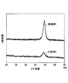
- FIG. 16 is a second view of the example of the manufacturing steps of the strain gauge of the first embodiment of the present invention; It is a figure which shows the result of the fluorescent-X-ray analysis of a functional layer. It is a figure which shows the result of X-ray diffraction of a resistor.
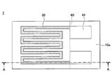
- FIG. 1 is a plan view illustrating a strain gauge according to a first embodiment.
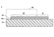
- FIG. 2 is a cross-sectional view illustrating the strain gauge according to the first embodiment, and shows a cross-section along the line AA of FIG.
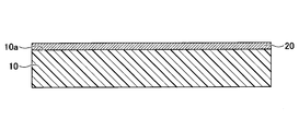
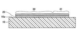
- the strain gauge 1 includes a base 10, a functional layer 20, a resistor 30, and a terminal portion 41.
- the side of the base material 10 on which the resistor 30 is provided is the upper side or one side, and the side on which the resistor 30 is not provided is the lower side or the other side.
- the surface on the side where the resistor 30 of each part is provided is referred to as one surface or upper surface, and the surface on the side where the resistor 30 is not provided is referred to as the other surface or lower surface.
- the strain gauge 1 can be used in the upside-down state or can be disposed at any angle.
- planar view refers to viewing the object in the normal direction of the upper surface 10a of the base material
- planar shape refers to a shape of the object viewed in the normal direction of the upper surface 10a of the base 10 I assume.
- the base 10 is a member to be a base layer for forming the resistor 30 and the like, and has flexibility.
- the thickness of the substrate 10 is not particularly limited and may be appropriately selected according to the purpose. For example, the thickness may be about 5 ⁇ m to 500 ⁇ m. In particular, when the thickness of the base material 10 is 5 ⁇ m to 200 ⁇ m, in terms of the transmission of strain from the surface of the strain-generating body joined to the lower surface of the base material 10 via the adhesive layer etc.
- the thickness is preferably 10 ⁇ m or more, further preferably in terms of insulation.
- the substrate 10 is made of, for example, PI (polyimide) resin, epoxy resin, PEEK (polyether ether ketone) resin, PEN (polyethylene naphthalate) resin, PET (polyethylene terephthalate) resin, PPS (polyphenylene sulfide) resin, polyolefin resin, etc.
- PI polyimide
- epoxy resin epoxy resin
- PEEK polyether ether ketone
- PEN polyethylene naphthalate
- PET polyethylene terephthalate
- PPS polyphenylene sulfide
- the substrate 10 may be formed of, for example, an insulating resin film containing a filler such as silica or alumina.
- the functional layer 20 is formed on the upper surface 10 a of the substrate 10 as a lower layer of the resistor 30. That is, the planar shape of the functional layer 20 is substantially the same as the planar shape of the resistor 30 shown in FIG.
- the thickness of the functional layer 20 can be, for example, about 1 nm to 100 nm.
- the functional layer refers to a layer having a function of promoting crystal growth of the resistor 30 which is at least the upper layer.
- the functional layer 20 preferably further has a function of preventing oxidation of the resistor 30 due to oxygen and moisture contained in the substrate 10, and a function of improving the adhesion between the substrate 10 and the resistor 30.
- the functional layer 20 may further have other functions.
- the insulating resin film constituting the substrate 10 contains oxygen and moisture, in particular when the resistor 30 contains Cr (chromium), the Cr forms a self-oxidized film, so the functional layer 20 oxidizes the resistor 30. It is effective to provide the function to prevent.
- the material of the functional layer 20 is not particularly limited as long as it has a function of promoting crystal growth of the resistor 30 which is at least the upper layer, and can be appropriately selected according to the purpose.
- Cr chromium
- Ti Ti
- V vanadium
- Nb niobium
- Ta tantalum
- Ni nickel
- Y yttrium
- Zr zirconium
- Hf hafnium
- Si silicon
- C carbon
- Cu copper
- Bi bismuth
- Fe iron
- Mo mobdenum
- W tungsten
- Ru ruthenium
- Rh Rhodium
- Re rhenium
- Os osmium
- Ir Iridium
- Pt platinum
- Pd palladium
- Ag silver
- Au gold
- Co cobalt
- Mn manganese
- Al aluminum
- One or more metals is-option, either metal alloys of this group, or
- FeCr, TiAl, FeNi, NiCr, CrCu etc. are mentioned, for example.
- As the above-mentioned compounds e.g., TiN, TaN, Si 3 N 4, TiO 2, Ta 2 O 5, SiO 2 , and the like.
- the resistor 30 is a thin film formed in a predetermined pattern on the upper surface of the functional layer 20, and is a sensing unit that receives strain and causes a change in resistance. In FIG. 1, for the sake of convenience, the resistor 30 is shown in a satin pattern.
- the resistor 30 can be formed of, for example, a material containing Cr (chromium), a material containing Ni (nickel), or a material containing both Cr and Ni. That is, the resistor 30 can be formed of a material containing at least one of Cr and Ni.
- a material containing Cr for example, a Cr multiphase film can be mentioned.
- a material containing Ni for example, Cu—Ni (copper nickel) can be mentioned.
- Ni-Cr nickel chromium
- the Cr multiphase film is a film in which Cr, CrN, Cr 2 N, etc. are mixed in phase.
- the Cr mixed phase film may contain unavoidable impurities such as chromium oxide.
- a part of the material constituting the functional layer 20 may be diffused into the Cr mixed phase film.
- the material constituting the functional layer 20 and nitrogen may form a compound.
- the Cr mixed phase film may contain Ti or TiN (titanium nitride).
- the thickness of the resistor 30 is not particularly limited and can be appropriately selected according to the purpose.
- the thickness can be set to about 0.05 ⁇ m to 2 ⁇ m.
- the thickness of the resistor 30 is 0.1 ⁇ m or more in that the crystallinity (for example, the crystallinity of ⁇ -Cr) of the crystals constituting the resistor 30 is improved, and the resistor of 1 ⁇ m or less It is further preferable in that it is possible to reduce the cracks of the film resulting from the internal stress of the film constituting 30 and the warpage from the base material 10.
- the resistor 30 By forming the resistor 30 on the functional layer 20, the resistor 30 can be formed with a stable crystal phase, so the stability of the gauge characteristics (gauge factor, gauge factor temperature coefficient TCS, and resistance temperature coefficient TCR) is improved. can do.
- the resistor 30 when the resistor 30 is a Cr mixed phase film, by providing the functional layer 20, the resistor 30 mainly composed of ⁇ -Cr (alpha chromium) can be formed. Since ⁇ -Cr is a stable crystal phase, the stability of the gauge characteristics can be improved.
- the main component means that the target substance occupies 50% by mass or more of all the substances constituting the resistor.
- the resistor 30 preferably contains 80% by weight or more of ⁇ -Cr from the viewpoint of improving the gauge characteristics.
- ⁇ -Cr is Cr of the bcc structure (body-centered cubic lattice structure).
- the metal (for example, Ti) constituting the functional layer 20 diffuses into the Cr mixed phase film, whereby the gauge characteristics can be improved.
- the gauge factor of the strain gauge 1 can be 10 or more, and the gauge factor temperature coefficient TCS and the resistance temperature coefficient TCR can be in the range of -1000 ppm / ° C to +1000 ppm / ° C.
- the terminal portion 41 extends from both ends of the resistor 30, and is wider than the resistor 30 and formed in a substantially rectangular shape in a plan view.
- the terminal portions 41 are a pair of electrodes for outputting a change in the resistance value of the resistor 30 caused by strain to the outside, and for example, a lead wire for external connection is joined.
- the resistor 30 extends, for example, from one of the terminal portions 41 in a zigzag manner and is connected to the other terminal portion 41.
- the upper surface of the terminal portion 41 may be coated with a metal having a better solderability than the terminal portion 41.
- the resistor 30 and the terminal part 41 are made into another code
- a cover layer 60 (insulating resin layer) may be provided on the upper surface 10 a of the base 10 so as to cover the resistor 30 and expose the terminal portion 41.
- the cover layer 60 may be provided so as to cover the entire portion excluding the terminal portion 41.
- the cover layer 60 can be formed of, for example, an insulating resin such as PI resin, epoxy resin, PEEK resin, PEN resin, PET resin, PPS resin, composite resin (for example, silicone resin, polyolefin resin).
- the cover layer 60 may contain a filler or a pigment.
- the thickness of the cover layer 60 is not particularly limited and may be appropriately selected depending on the purpose. For example, the thickness may be about 2 ⁇ m to 30 ⁇ m.
- FIGS. 3A and 3B are views illustrating the manufacturing process of the strain gauge according to the first embodiment, and show a cross section corresponding to FIG.
- the base material 10 is prepared, and the functional layer 20 is formed on the upper surface 10 a of the base material 10.
- the materials and thicknesses of the base 10 and the functional layer 20 are as described above.
- the functional layer 20 can be vacuum deposited, for example, by a conventional sputtering method in which Ar (argon) gas is introduced into the chamber with a source capable of forming the functional layer 20 as a target.
- Ar argon
- the functional layer 20 is formed while etching the upper surface 10 a of the substrate 10 with Ar, so that the amount of forming the functional layer 20 can be minimized to obtain the adhesion improvement effect. it can.
- the functional layer 20 may be formed by another method.
- the adhesion improvement effect is obtained by activating the upper surface 10a of the substrate 10 by plasma treatment using Ar or the like before film formation of the functional layer 20, and then the functional layer 20 is vacuum-deposited by magnetron sputtering.
- a method of film formation may be used.
- the functional layer 20 and the resistor 30 and the terminal portion 41 are formed into the planar shape shown in FIG. Pattern it.
- the materials and thicknesses of the resistor 30 and the terminal portion 41 are as described above.
- the resistor 30 and the terminal portion 41 can be integrally formed of the same material.
- the resistor 30 and the terminal portion 41 can be formed, for example, by a magnetron sputtering method using a raw material capable of forming the resistor 30 and the terminal portion 41 as a target.
- the resistor 30 and the terminal portion 41 may be formed by reactive sputtering, evaporation, arc ion plating, pulsed laser deposition, or the like, instead of the magnetron sputtering.
- the combination of the material of the functional layer 20 and the material of the resistor 30 and the terminal portion 41 is not particularly limited and may be appropriately selected according to the purpose.
- Ti is used as the functional layer 20, and the resistor 30 and the terminal portion It is possible to form a Cr mixed phase film containing ⁇ -Cr (alpha chromium) as a main component as 41.
- the resistor 30 and the terminal portion 41 can be formed by a magnetron sputtering method in which Ar gas is introduced into the chamber with a raw material capable of forming a Cr mixed phase film as a target.
- Ar gas is introduced into the chamber with a raw material capable of forming a Cr mixed phase film as a target.
- pure Cr may be used as a target
- an appropriate amount of nitrogen gas may be introduced into the chamber together with Ar gas, and the resistor 30 and the terminal portion 41 may be formed by reactive sputtering.
- the growth surface of the Cr multi-phase film is defined by the functional layer 20 made of Ti as a trigger, and a Cr multi-phase film mainly composed of ⁇ -Cr having a stable crystal structure can be formed. Further, the diffusion of Ti constituting the functional layer 20 into the Cr multiphase film improves the gauge characteristics.
- the gauge factor of the strain gauge 1 can be 10 or more, and the gauge factor temperature coefficient TCS and the resistance temperature coefficient TCR can be in the range of -1000 ppm / ° C to +1000 ppm / ° C.
- the functional layer 20 made of Ti has a function of promoting crystal growth of the resistor 30, and prevents the oxidation of the resistor 30 due to oxygen and moisture contained in the base material 10. All of the functions and functions to improve the adhesion between the substrate 10 and the resistor 30 are provided. The same applies to the case where Ta, Si, Al, or Fe is used as the functional layer 20 instead of Ti.
- the strain gauge 1 is completed by providing a cover layer 60 which covers the resistor 30 and exposes the terminal portion 41 on the upper surface 10a of the base 10, if necessary.
- the cover layer 60 is formed, for example, by laminating a thermosetting insulating resin film in a semi-hardened state on the upper surface 10 a of the base 10 so as to cover the resistor 30 and expose the terminal portion 41 and heat and cure it. It can be made.
- the cover layer 60 is formed by applying a liquid or paste-like thermosetting insulating resin on the upper surface 10 a of the base 10 so as to cover the resistor 30 and expose the terminal portion 41, and heat and cure it. May be
- the functional layer 20 in the lower layer of the resistor 30, it is possible to promote crystal growth of the resistor 30, and the resistor 30 composed of a stable crystal phase can be manufactured. As a result, in the strain gauge 1, the stability of the gauge characteristics can be improved. Further, the material constituting the functional layer 20 diffuses into the resistor 30, whereby the gauge characteristics of the strain gauge 1 can be improved.
- Example 1 First, as a preliminary experiment, Ti was vacuum-deposited as the functional layer 20 on the upper surface 10a of the substrate 10 made of polyimide resin with a thickness of 25 ⁇ m by conventional sputtering. Under the present circumstances, five samples which formed Ti film-forming aiming at several film thickness were produced.
- XRF fluorescent X-ray
- Example 1 Ti with a film thickness of 3 nm was vacuum-deposited as a functional layer 20 on the upper surface 10a of the substrate 10 made of polyimide resin with a thickness of 25 ⁇ m by conventional sputtering.
- the functional layer 20 and the resistor 30 and the terminal portion 41 are photolithographically as shown in FIG. Patterned.
- a Cr multiphase film is formed as the resistor 30 and the terminal portion 41 by the magnetron sputtering method without forming the functional layer 20 on the upper surface 10a of the substrate 10 made of polyimide resin with a thickness of 25 ⁇ m. And patterned as in FIG. 1 by photolithography.
- the film forming conditions of the resistor 30 and the terminal portion 41 are all the same.
- FIG. 5 is an X-ray diffraction pattern in a diffraction angle of 2 ⁇ of 36 to 48 degrees, and the diffraction peak of Example 1 is shifted to the right of the diffraction peak of Comparative Example 1. Moreover, the diffraction peak of Example 1 is higher than the diffraction peak of Comparative Example 1.
- Example 1 The diffraction peak of Example 1 is located in the vicinity of the diffraction line of ⁇ -Cr (110), and by providing the functional layer 20 made of Ti, the crystal growth of ⁇ -Cr is promoted to become ⁇ -Cr. It is considered that a Cr multi-phase film containing as a main component is formed.
- Example 1 a plurality of samples of Example 1 and a sample of Comparative Example 1 were produced, and gauge characteristics were measured. As a result, the gauge factor of each sample of Example 1 was 14 to 16, while the gauge factor of each sample of Comparative Example 1 was less than 10.
- the gauge temperature coefficient TCS and the resistance temperature coefficient TCR of each sample of Example 1 were within the range of -1000 ppm / ° C to +1000 ppm / ° C
- the gauge temperature coefficient TCS of each sample of Comparative Example 1 was And, the temperature coefficient of resistance TCR did not fall within the range of -1000 ppm / ° C to +1000 ppm / ° C.
- the functional layer 20 made of Ti crystal growth of ⁇ -Cr is promoted to form a Cr multi-phase film mainly composed of ⁇ -Cr, and the gauge factor is 10 or more, and the gauge factor A strain gauge having a temperature coefficient TCS and a temperature coefficient of resistance TCR of -1000 ppm / ° C. to +1000 ppm / ° C. was produced. It is considered that the diffusion effect of Ti to the Cr mixed phase film contributes to the improvement of the gauge characteristics.
Abstract
This strain gauge has a flexible substrate, a functional layer formed from a metal, an alloy, or a metal compound on one surface of the substrate, and a resistor formed from a material containing chromium and/or nickel on one surface of the functional layer.
Description
本発明は、ひずみゲージに関する。
The present invention relates to strain gauges.
測定対象物に貼り付けて、測定対象物のひずみを検出するひずみゲージが知られている。ひずみゲージは、ひずみを検出する抵抗体を備えており、抵抗体の材料としては、例えば、Cr(クロム)やNi(ニッケル)を含む材料が用いられている。又、抵抗体は、例えば、絶縁樹脂からなる基材上に形成されている(例えば、特許文献1参照)。
There is known a strain gauge which is attached to a measurement object to detect a strain of the measurement object. The strain gauge includes a resistor that detects strain, and a material containing, for example, Cr (chromium) or Ni (nickel) is used as a material of the resistor. The resistor is formed on, for example, a base made of an insulating resin (see, for example, Patent Document 1).
しかしながら、可撓性を有する基材を用いた場合、基材上に安定な抵抗体を形成することは困難であり、ゲージ特性(ゲージ率、ゲージ率温度係数TCS、及び抵抗温度係数TCR)の安定性に欠けるという問題があった。
However, when a flexible base material is used, it is difficult to form a stable resistor on the base material, and the gauge characteristics (gauge factor, gauge factor temperature coefficient TCS, and resistance temperature coefficient TCR) are obtained. There was a problem of lack of stability.
本発明は、上記の点に鑑みてなされたもので、可撓性を有する基材上に形成された抵抗体を有するひずみゲージにおいて、ゲージ特性の安定性を向上することを目的とする。
The present invention has been made in view of the above-described point, and an object of the present invention is to improve the stability of gauge characteristics in a strain gauge having a resistor formed on a flexible base material.
本ひずみゲージは、可撓性を有する基材と、前記基材の一方の面に、金属、合金、又は、金属の化合物から形成された機能層と、前記機能層の一方の面に、クロムとニッケルの少なくとも一方を含む材料から形成された抵抗体と、を有する。
The present strain gauge comprises a flexible substrate, a functional layer formed of a metal, an alloy, or a compound of metal on one surface of the substrate, and chromium on one surface of the functional layer. And a resistor formed of a material containing at least one of nickel and nickel.
開示の技術によれば、可撓性を有する基材上に形成された抵抗体を有するひずみゲージにおいて、ゲージ特性の安定性を向上することができる。
According to the disclosed technology, the stability of gauge characteristics can be improved in a strain gauge having a resistor formed on a flexible substrate.
以下、図面を参照して発明を実施するための形態について説明する。各図面において、同一構成部分には同一符号を付し、重複した説明を省略する場合がある。
Hereinafter, embodiments of the present invention will be described with reference to the drawings. In the drawings, the same components are denoted by the same reference numerals, and redundant description may be omitted.
〈第1の実施の形態〉
図1は、第1の実施の形態に係るひずみゲージを例示する平面図である。図2は、第1の実施の形態に係るひずみゲージを例示する断面図であり、図1のA-A線に沿う断面を示している。図1及び図2を参照するに、ひずみゲージ1は、基材10と、機能層20と、抵抗体30と、端子部41とを有している。 First Embodiment
FIG. 1 is a plan view illustrating a strain gauge according to a first embodiment. FIG. 2 is a cross-sectional view illustrating the strain gauge according to the first embodiment, and shows a cross-section along the line AA of FIG. Referring to FIGS. 1 and 2, thestrain gauge 1 includes a base 10, a functional layer 20, a resistor 30, and a terminal portion 41.
図1は、第1の実施の形態に係るひずみゲージを例示する平面図である。図2は、第1の実施の形態に係るひずみゲージを例示する断面図であり、図1のA-A線に沿う断面を示している。図1及び図2を参照するに、ひずみゲージ1は、基材10と、機能層20と、抵抗体30と、端子部41とを有している。 First Embodiment
FIG. 1 is a plan view illustrating a strain gauge according to a first embodiment. FIG. 2 is a cross-sectional view illustrating the strain gauge according to the first embodiment, and shows a cross-section along the line AA of FIG. Referring to FIGS. 1 and 2, the
なお、本実施の形態では、便宜上、ひずみゲージ1において、基材10の抵抗体30が設けられている側を上側又は一方の側、抵抗体30が設けられていない側を下側又は他方の側とする。又、各部位の抵抗体30が設けられている側の面を一方の面又は上面、抵抗体30が設けられていない側の面を他方の面又は下面とする。但し、ひずみゲージ1は天地逆の状態で用いることができ、又は任意の角度で配置することができる。又、平面視とは対象物を基材10の上面10aの法線方向から視ることを指し、平面形状とは対象物を基材10の上面10aの法線方向から視た形状を指すものとする。
In the present embodiment, for convenience, in the strain gauge 1, the side of the base material 10 on which the resistor 30 is provided is the upper side or one side, and the side on which the resistor 30 is not provided is the lower side or the other side. To the side. Further, the surface on the side where the resistor 30 of each part is provided is referred to as one surface or upper surface, and the surface on the side where the resistor 30 is not provided is referred to as the other surface or lower surface. However, the strain gauge 1 can be used in the upside-down state or can be disposed at any angle. Further, planar view refers to viewing the object in the normal direction of the upper surface 10a of the base material 10, and planar shape refers to a shape of the object viewed in the normal direction of the upper surface 10a of the base 10 I assume.
基材10は、抵抗体30等を形成するためのベース層となる部材であり、可撓性を有する。基材10の厚さは、特に制限はなく、目的に応じて適宜選択できるが、例えば、5μm~500μm程度とすることができる。特に、基材10の厚さが5μm~200μmであると、接着層等を介して基材10の下面に接合される起歪体表面からの歪の伝達性、環境に対する寸法安定性の点で好ましく、10μm以上であると絶縁性の点で更に好ましい。
The base 10 is a member to be a base layer for forming the resistor 30 and the like, and has flexibility. The thickness of the substrate 10 is not particularly limited and may be appropriately selected according to the purpose. For example, the thickness may be about 5 μm to 500 μm. In particular, when the thickness of the base material 10 is 5 μm to 200 μm, in terms of the transmission of strain from the surface of the strain-generating body joined to the lower surface of the base material 10 via the adhesive layer etc. The thickness is preferably 10 μm or more, further preferably in terms of insulation.
基材10は、例えば、PI(ポリイミド)樹脂、エポキシ樹脂、PEEK(ポリエーテルエーテルケトン)樹脂、PEN(ポリエチレンナフタレート)樹脂、PET(ポリエチレンテレフタレート)樹脂、PPS(ポリフェニレンサルファイド)樹脂、ポリオレフィン樹脂等の絶縁樹脂フィルムから形成することができる。なお、フィルムとは、厚さが500μm以下程度であり、可撓性を有する部材を指す。
The substrate 10 is made of, for example, PI (polyimide) resin, epoxy resin, PEEK (polyether ether ketone) resin, PEN (polyethylene naphthalate) resin, PET (polyethylene terephthalate) resin, PPS (polyphenylene sulfide) resin, polyolefin resin, etc. The insulating resin film of In addition, a film is about 500 micrometers or less in thickness, and points out the member which has flexibility.
ここで、『絶縁樹脂フィルムから形成する』とは、基材10が絶縁樹脂フィルム中にフィラーや不純物等を含有することを妨げるものではない。基材10は、例えば、シリカやアルミナ等のフィラーを含有する絶縁樹脂フィルムから形成しても構わない。
Here, "forming from an insulating resin film" does not prevent the base material 10 from containing a filler, an impurity, and the like in the insulating resin film. The substrate 10 may be formed of, for example, an insulating resin film containing a filler such as silica or alumina.
機能層20は、基材10の上面10aに抵抗体30の下層として形成されている。すなわち、機能層20の平面形状は、図1に示す抵抗体30の平面形状と略同一である。機能層20の厚さは、例えば、1nm~100nm程度とすることができる。
The functional layer 20 is formed on the upper surface 10 a of the substrate 10 as a lower layer of the resistor 30. That is, the planar shape of the functional layer 20 is substantially the same as the planar shape of the resistor 30 shown in FIG. The thickness of the functional layer 20 can be, for example, about 1 nm to 100 nm.
本願において、機能層とは、少なくとも上層である抵抗体30の結晶成長を促進する機能を有する層を指す。機能層20は、更に、基材10に含まれる酸素や水分による抵抗体30の酸化を防止する機能や、基材10と抵抗体30との密着性を向上する機能を備えていることが好ましい。機能層20は、更に、他の機能を備えていてもよい。
In the present application, the functional layer refers to a layer having a function of promoting crystal growth of the resistor 30 which is at least the upper layer. The functional layer 20 preferably further has a function of preventing oxidation of the resistor 30 due to oxygen and moisture contained in the substrate 10, and a function of improving the adhesion between the substrate 10 and the resistor 30. . The functional layer 20 may further have other functions.
基材10を構成する絶縁樹脂フィルムは酸素や水分を含むため、特に抵抗体30がCr(クロム)を含む場合、Crは自己酸化膜を形成するため、機能層20が抵抗体30の酸化を防止する機能を備えることは有効である。
Since the insulating resin film constituting the substrate 10 contains oxygen and moisture, in particular when the resistor 30 contains Cr (chromium), the Cr forms a self-oxidized film, so the functional layer 20 oxidizes the resistor 30. It is effective to provide the function to prevent.
機能層20の材料は、少なくとも上層である抵抗体30の結晶成長を促進する機能を有する材料であれば、特に制限はなく、目的に応じて適宜選択できるが、例えば、Cr(クロム)、Ti(チタン)、V(バナジウム)、Nb(ニオブ)、Ta(タンタル)、Ni(ニッケル)、Y(イットリウム)、Zr(ジルコニウム)、Hf(ハフニウム)、Si(シリコン)、C(炭素)、Zn(亜鉛)、Cu(銅)、Bi(ビスマス)、Fe(鉄)、Mo(モリブデン)、W(タングステン)、Ru(ルテニウム)、Rh(ロジウム)、Re(レニウム)、Os(オスミウム)、Ir(イリジウム)、Pt(白金)、Pd(パラジウム)、Ag(銀)、Au(金)、Co(コバルト)、Mn(マンガン)、Al(アルミニウム)からなる群から選択される1種又は複数種の金属、この群の何れかの金属の合金、又は、この群の何れかの金属の化合物が挙げられる。
The material of the functional layer 20 is not particularly limited as long as it has a function of promoting crystal growth of the resistor 30 which is at least the upper layer, and can be appropriately selected according to the purpose. For example, Cr (chromium) or Ti (Titanium), V (vanadium), Nb (niobium), Ta (tantalum), Ni (nickel), Y (yttrium), Zr (zirconium), Hf (hafnium), Si (silicon), C (carbon), Zn (Zinc), Cu (copper), Bi (bismuth), Fe (iron), Mo (molybdenum), W (tungsten), Ru (ruthenium), Rh (rhodium), Re (rhenium), Os (osmium), Ir (Iridium), Pt (platinum), Pd (palladium), Ag (silver), Au (gold), Co (cobalt), Mn (manganese), Al (aluminum) One or more metals is-option, either metal alloys of this group, or a compound of any one of metals of this group and the like.
上記の合金としては、例えば、FeCr、TiAl、FeNi、NiCr、CrCu等が挙げられる。又、上記の化合物としては、例えば、TiN、TaN、Si3N4、TiO2、Ta2O5、SiO2等が挙げられる。
As said alloy, FeCr, TiAl, FeNi, NiCr, CrCu etc. are mentioned, for example. As the above-mentioned compounds, e.g., TiN, TaN, Si 3 N 4, TiO 2, Ta 2 O 5, SiO 2 , and the like.
抵抗体30は、機能層20の上面に所定のパターンで形成された薄膜であり、ひずみを受けて抵抗変化を生じる受感部である。なお、図1では、便宜上、抵抗体30を梨地模様で示している。
The resistor 30 is a thin film formed in a predetermined pattern on the upper surface of the functional layer 20, and is a sensing unit that receives strain and causes a change in resistance. In FIG. 1, for the sake of convenience, the resistor 30 is shown in a satin pattern.
抵抗体30は、例えば、Cr(クロム)を含む材料、Ni(ニッケル)を含む材料、又はCrとNiの両方を含む材料から形成することができる。すなわち、抵抗体30は、CrとNiの少なくとも一方を含む材料から形成することができる。Crを含む材料としては、例えば、Cr混相膜が挙げられる。Niを含む材料としては、例えば、Cu-Ni(銅ニッケル)が挙げられる。CrとNiの両方を含む材料としては、例えば、Ni-Cr(ニッケルクロム)が挙げられる。
The resistor 30 can be formed of, for example, a material containing Cr (chromium), a material containing Ni (nickel), or a material containing both Cr and Ni. That is, the resistor 30 can be formed of a material containing at least one of Cr and Ni. As a material containing Cr, for example, a Cr multiphase film can be mentioned. As a material containing Ni, for example, Cu—Ni (copper nickel) can be mentioned. As a material containing both Cr and Ni, for example, Ni-Cr (nickel chromium) can be mentioned.
ここで、Cr混相膜とは、Cr、CrN、Cr2N等が混相した膜である。Cr混相膜は、酸化クロム等の不可避不純物を含んでもよい。又、Cr混相膜に、機能層20を構成する材料の一部が拡散されてもよい。この場合、機能層20を構成する材料と窒素とが化合物を形成する場合もある。例えば、機能層20がTiから形成されている場合、Cr混相膜にTiやTiN(窒化チタン)が含まれる場合がある。
Here, the Cr multiphase film is a film in which Cr, CrN, Cr 2 N, etc. are mixed in phase. The Cr mixed phase film may contain unavoidable impurities such as chromium oxide. In addition, a part of the material constituting the functional layer 20 may be diffused into the Cr mixed phase film. In this case, the material constituting the functional layer 20 and nitrogen may form a compound. For example, when the functional layer 20 is formed of Ti, the Cr mixed phase film may contain Ti or TiN (titanium nitride).
抵抗体30の厚さは、特に制限はなく、目的に応じて適宜選択できるが、例えば、0.05μm~2μm程度とすることができる。特に、抵抗体30の厚さが0.1μm以上であると抵抗体30を構成する結晶の結晶性(例えば、α-Crの結晶性)が向上する点で好ましく、1μm以下であると抵抗体30を構成する膜の内部応力に起因する膜のクラックや基材10からの反りを低減できる点で更に好ましい。
The thickness of the resistor 30 is not particularly limited and can be appropriately selected according to the purpose. For example, the thickness can be set to about 0.05 μm to 2 μm. In particular, it is preferable that the thickness of the resistor 30 is 0.1 μm or more in that the crystallinity (for example, the crystallinity of α-Cr) of the crystals constituting the resistor 30 is improved, and the resistor of 1 μm or less It is further preferable in that it is possible to reduce the cracks of the film resulting from the internal stress of the film constituting 30 and the warpage from the base material 10.
機能層20上に抵抗体30を形成することで、安定な結晶相により抵抗体30を形成できるため、ゲージ特性(ゲージ率、ゲージ率温度係数TCS、及び抵抗温度係数TCR)の安定性を向上することができる。
By forming the resistor 30 on the functional layer 20, the resistor 30 can be formed with a stable crystal phase, so the stability of the gauge characteristics (gauge factor, gauge factor temperature coefficient TCS, and resistance temperature coefficient TCR) is improved. can do.
例えば、抵抗体30がCr混相膜である場合、機能層20を設けることで、α-Cr(アルファクロム)を主成分とする抵抗体30を形成することができる。α-Crは安定な結晶相であるため、ゲージ特性の安定性を向上することができる。
For example, when the resistor 30 is a Cr mixed phase film, by providing the functional layer 20, the resistor 30 mainly composed of α-Cr (alpha chromium) can be formed. Since α-Cr is a stable crystal phase, the stability of the gauge characteristics can be improved.
ここで、主成分とは、対象物質が抵抗体を構成する全物質の50質量%以上を占めることを意味する。抵抗体30がCr混相膜である場合、ゲージ特性を向上する観点から、抵抗体30はα-Crを80重量%以上含むことが好ましい。なお、α-Crは、bcc構造(体心立方格子構造)のCrである。
Here, the main component means that the target substance occupies 50% by mass or more of all the substances constituting the resistor. When the resistor 30 is a Cr mixed phase film, the resistor 30 preferably contains 80% by weight or more of α-Cr from the viewpoint of improving the gauge characteristics. Here, α-Cr is Cr of the bcc structure (body-centered cubic lattice structure).
又、機能層20を構成する金属(例えば、Ti)がCr混相膜中に拡散することにより、ゲージ特性を向上することができる。具体的には、ひずみゲージ1のゲージ率を10以上、かつゲージ率温度係数TCS及び抵抗温度係数TCRを-1000ppm/℃~+1000ppm/℃の範囲内とすることができる。
Further, the metal (for example, Ti) constituting the functional layer 20 diffuses into the Cr mixed phase film, whereby the gauge characteristics can be improved. Specifically, the gauge factor of the strain gauge 1 can be 10 or more, and the gauge factor temperature coefficient TCS and the resistance temperature coefficient TCR can be in the range of -1000 ppm / ° C to +1000 ppm / ° C.
端子部41は、抵抗体30の両端部から延在しており、平面視において、抵抗体30よりも拡幅して略矩形状に形成されている。端子部41は、ひずみにより生じる抵抗体30の抵抗値の変化を外部に出力するための一対の電極であり、例えば、外部接続用のリード線等が接合される。抵抗体30は、例えば、端子部41の一方からジグザグに折り返しながら延在して他方の端子部41に接続されている。端子部41の上面を、端子部41よりもはんだ付け性が良好な金属で被覆してもよい。なお、抵抗体30と端子部41とは便宜上別符号としているが、両者は同一工程において同一材料により一体に形成することができる。
The terminal portion 41 extends from both ends of the resistor 30, and is wider than the resistor 30 and formed in a substantially rectangular shape in a plan view. The terminal portions 41 are a pair of electrodes for outputting a change in the resistance value of the resistor 30 caused by strain to the outside, and for example, a lead wire for external connection is joined. The resistor 30 extends, for example, from one of the terminal portions 41 in a zigzag manner and is connected to the other terminal portion 41. The upper surface of the terminal portion 41 may be coated with a metal having a better solderability than the terminal portion 41. In addition, although the resistor 30 and the terminal part 41 are made into another code | symbol for convenience, both can be integrally formed with the same material in the same process.
抵抗体30を被覆し端子部41を露出するように基材10の上面10aにカバー層60(絶縁樹脂層)を設けても構わない。カバー層60を設けることで、抵抗体30に機械的な損傷等が生じることを防止できる。又、カバー層60を設けることで、抵抗体30を湿気等から保護することができる。なお、カバー層60は、端子部41を除く部分の全体を覆うように設けてもよい。
A cover layer 60 (insulating resin layer) may be provided on the upper surface 10 a of the base 10 so as to cover the resistor 30 and expose the terminal portion 41. By providing the cover layer 60, it is possible to prevent mechanical damage or the like from occurring in the resistor 30. Further, by providing the cover layer 60, the resistor 30 can be protected from moisture and the like. The cover layer 60 may be provided so as to cover the entire portion excluding the terminal portion 41.
カバー層60は、例えば、PI樹脂、エポキシ樹脂、PEEK樹脂、PEN樹脂、PET樹脂、PPS樹脂、複合樹脂(例えば、シリコーン樹脂、ポリオレフィン樹脂)等の絶縁樹脂から形成することができる。カバー層60は、フィラーや顔料を含有しても構わない。カバー層60の厚さは、特に制限はなく、目的に応じて適宜選択できるが、例えば、2μm~30μm程度とすることができる。
The cover layer 60 can be formed of, for example, an insulating resin such as PI resin, epoxy resin, PEEK resin, PEN resin, PET resin, PPS resin, composite resin (for example, silicone resin, polyolefin resin). The cover layer 60 may contain a filler or a pigment. The thickness of the cover layer 60 is not particularly limited and may be appropriately selected depending on the purpose. For example, the thickness may be about 2 μm to 30 μm.
図3A及び図3Bは、第1の実施の形態に係るひずみゲージの製造工程を例示する図であり、図2に対応する断面を示している。ひずみゲージ1を製造するためには、まず、図3Aに示す工程では、基材10を準備し、基材10の上面10aに機能層20を形成する。基材10及び機能層20の材料や厚さは、前述の通りである。
FIGS. 3A and 3B are views illustrating the manufacturing process of the strain gauge according to the first embodiment, and show a cross section corresponding to FIG. In order to manufacture the strain gauge 1, first, in the process illustrated in FIG. 3A, the base material 10 is prepared, and the functional layer 20 is formed on the upper surface 10 a of the base material 10. The materials and thicknesses of the base 10 and the functional layer 20 are as described above.
機能層20は、例えば、機能層20を形成可能な原料をターゲットとし、チャンバ内にAr(アルゴン)ガスを導入したコンベンショナルスパッタ法により真空成膜することができる。コンベンショナルスパッタ法を用いることにより、基材10の上面10aをArでエッチングしながら機能層20が成膜されるため、機能層20の成膜量を最小限にして密着性改善効果を得ることができる。
The functional layer 20 can be vacuum deposited, for example, by a conventional sputtering method in which Ar (argon) gas is introduced into the chamber with a source capable of forming the functional layer 20 as a target. By using the conventional sputtering method, the functional layer 20 is formed while etching the upper surface 10 a of the substrate 10 with Ar, so that the amount of forming the functional layer 20 can be minimized to obtain the adhesion improvement effect. it can.
但し、これは、機能層20の成膜方法の一例であり、他の方法により機能層20を成膜してもよい。例えば、機能層20の成膜の前にAr等を用いたプラズマ処理等により基材10の上面10aを活性化することで密着性改善効果を獲得し、その後マグネトロンスパッタ法により機能層20を真空成膜する方法を用いてもよい。
However, this is an example of a method of forming the functional layer 20, and the functional layer 20 may be formed by another method. For example, the adhesion improvement effect is obtained by activating the upper surface 10a of the substrate 10 by plasma treatment using Ar or the like before film formation of the functional layer 20, and then the functional layer 20 is vacuum-deposited by magnetron sputtering. A method of film formation may be used.
次に、図3Bに示す工程では、機能層20の上面全体に抵抗体30及び端子部41を形成後、フォトリソグラフィによって機能層20並びに抵抗体30及び端子部41を図1に示す平面形状にパターニングする。抵抗体30及び端子部41の材料や厚さは、前述の通りである。抵抗体30と端子部41とは、同一材料により一体に形成することができる。抵抗体30及び端子部41は、例えば、抵抗体30及び端子部41を形成可能な原料をターゲットとしたマグネトロンスパッタ法により成膜することができる。抵抗体30及び端子部41は、マグネトロンスパッタ法に代えて、反応性スパッタ法や蒸着法、アークイオンプレーティング法、パルスレーザー堆積法等を用いて成膜してもよい。
Next, in the process shown in FIG. 3B, after the resistor 30 and the terminal portion 41 are formed on the entire upper surface of the functional layer 20, the functional layer 20 and the resistor 30 and the terminal portion 41 are formed into the planar shape shown in FIG. Pattern it. The materials and thicknesses of the resistor 30 and the terminal portion 41 are as described above. The resistor 30 and the terminal portion 41 can be integrally formed of the same material. The resistor 30 and the terminal portion 41 can be formed, for example, by a magnetron sputtering method using a raw material capable of forming the resistor 30 and the terminal portion 41 as a target. The resistor 30 and the terminal portion 41 may be formed by reactive sputtering, evaporation, arc ion plating, pulsed laser deposition, or the like, instead of the magnetron sputtering.
機能層20の材料と抵抗体30及び端子部41の材料との組み合わせは、特に制限はなく、目的に応じて適宜選択できるが、例えば、機能層20としてTiを用い、抵抗体30及び端子部41としてα-Cr(アルファクロム)を主成分とするCr混相膜を成膜することが可能である。
The combination of the material of the functional layer 20 and the material of the resistor 30 and the terminal portion 41 is not particularly limited and may be appropriately selected according to the purpose. For example, Ti is used as the functional layer 20, and the resistor 30 and the terminal portion It is possible to form a Cr mixed phase film containing α-Cr (alpha chromium) as a main component as 41.
この場合、例えば、Cr混相膜を形成可能な原料をターゲットとし、チャンバ内にArガスを導入したマグネトロンスパッタ法により、抵抗体30及び端子部41を成膜することができる。或いは、純Crをターゲットとし、チャンバ内にArガスと共に適量の窒素ガスを導入し、反応性スパッタ法により、抵抗体30及び端子部41を成膜してもよい。
In this case, for example, the resistor 30 and the terminal portion 41 can be formed by a magnetron sputtering method in which Ar gas is introduced into the chamber with a raw material capable of forming a Cr mixed phase film as a target. Alternatively, pure Cr may be used as a target, an appropriate amount of nitrogen gas may be introduced into the chamber together with Ar gas, and the resistor 30 and the terminal portion 41 may be formed by reactive sputtering.
これらの方法では、Tiからなる機能層20がきっかけでCr混相膜の成長面が規定され、安定な結晶構造であるα-Crを主成分とするCr混相膜を成膜できる。又、機能層20を構成するTiがCr混相膜中に拡散することにより、ゲージ特性が向上する。例えば、ひずみゲージ1のゲージ率を10以上、かつゲージ率温度係数TCS及び抵抗温度係数TCRを-1000ppm/℃~+1000ppm/℃の範囲内とすることができる。
In these methods, the growth surface of the Cr multi-phase film is defined by the functional layer 20 made of Ti as a trigger, and a Cr multi-phase film mainly composed of α-Cr having a stable crystal structure can be formed. Further, the diffusion of Ti constituting the functional layer 20 into the Cr multiphase film improves the gauge characteristics. For example, the gauge factor of the strain gauge 1 can be 10 or more, and the gauge factor temperature coefficient TCS and the resistance temperature coefficient TCR can be in the range of -1000 ppm / ° C to +1000 ppm / ° C.
なお、抵抗体30がCr混相膜である場合、Tiからなる機能層20は、抵抗体30の結晶成長を促進する機能、基材10に含まれる酸素や水分による抵抗体30の酸化を防止する機能、及び基材10と抵抗体30との密着性を向上する機能の全てを備えている。機能層20として、Tiに代えてTa、Si、Al、Feを用いた場合も同様である。
When the resistor 30 is a Cr mixed phase film, the functional layer 20 made of Ti has a function of promoting crystal growth of the resistor 30, and prevents the oxidation of the resistor 30 due to oxygen and moisture contained in the base material 10. All of the functions and functions to improve the adhesion between the substrate 10 and the resistor 30 are provided. The same applies to the case where Ta, Si, Al, or Fe is used as the functional layer 20 instead of Ti.
図3Bに示す工程の後、必要に応じ、基材10の上面10aに、抵抗体30を被覆し端子部41を露出するカバー層60を設けることで、ひずみゲージ1が完成する。カバー層60は、例えば、基材10の上面10aに、抵抗体30を被覆し端子部41を露出するように半硬化状態の熱硬化性の絶縁樹脂フィルムをラミネートし、加熱して硬化させて作製することができる。カバー層60は、基材10の上面10aに、抵抗体30を被覆し端子部41を露出するように液状又はペースト状の熱硬化性の絶縁樹脂を塗布し、加熱して硬化させて作製してもよい。
After the process shown in FIG. 3B, the strain gauge 1 is completed by providing a cover layer 60 which covers the resistor 30 and exposes the terminal portion 41 on the upper surface 10a of the base 10, if necessary. The cover layer 60 is formed, for example, by laminating a thermosetting insulating resin film in a semi-hardened state on the upper surface 10 a of the base 10 so as to cover the resistor 30 and expose the terminal portion 41 and heat and cure it. It can be made. The cover layer 60 is formed by applying a liquid or paste-like thermosetting insulating resin on the upper surface 10 a of the base 10 so as to cover the resistor 30 and expose the terminal portion 41, and heat and cure it. May be
このように、抵抗体30の下層に機能層20を設けることにより、抵抗体30の結晶成長を促進することが可能となり、安定な結晶相からなる抵抗体30を作製できる。その結果、ひずみゲージ1において、ゲージ特性の安定性を向上することができる。又、機能層20を構成する材料が抵抗体30に拡散することにより、ひずみゲージ1において、ゲージ特性を向上することができる。
As described above, by providing the functional layer 20 in the lower layer of the resistor 30, it is possible to promote crystal growth of the resistor 30, and the resistor 30 composed of a stable crystal phase can be manufactured. As a result, in the strain gauge 1, the stability of the gauge characteristics can be improved. Further, the material constituting the functional layer 20 diffuses into the resistor 30, whereby the gauge characteristics of the strain gauge 1 can be improved.
[実施例1]
まず、事前実験として、厚さ25μmのポリイミド樹脂からなる基材10の上面10aに、コンベンショナルスパッタ法により機能層20としてTiを真空成膜した。この際、複数の膜厚を狙ってTiを成膜した5個のサンプルを作製した。 Example 1
First, as a preliminary experiment, Ti was vacuum-deposited as thefunctional layer 20 on the upper surface 10a of the substrate 10 made of polyimide resin with a thickness of 25 μm by conventional sputtering. Under the present circumstances, five samples which formed Ti film-forming aiming at several film thickness were produced.
まず、事前実験として、厚さ25μmのポリイミド樹脂からなる基材10の上面10aに、コンベンショナルスパッタ法により機能層20としてTiを真空成膜した。この際、複数の膜厚を狙ってTiを成膜した5個のサンプルを作製した。 Example 1
First, as a preliminary experiment, Ti was vacuum-deposited as the
次に、作製した5個のサンプルについて蛍光X線(XRF:X‐ray Fluorescence)分析を行い、図4に示す結果を得た。図4のX線ピークよりTiの存在が確認され、X線ピークにおける各々のサンプルのX線強度より、1nm~100nmの範囲でTi膜の膜厚が制御できることが確認された。
Next, fluorescent X-ray (XRF) analysis (XRF: XRF analysis) was performed on the five samples produced, and the results shown in FIG. 4 were obtained. The presence of Ti was confirmed from the X-ray peak in FIG. 4, and from the X-ray intensity of each sample at the X-ray peak, it was confirmed that the film thickness of the Ti film can be controlled in the range of 1 nm to 100 nm.
次に、実施例1として、厚さ25μmのポリイミド樹脂からなる基材10の上面10aに、コンベンショナルスパッタ法により機能層20として膜厚が3nmのTiを真空成膜した。
Next, as Example 1, Ti with a film thickness of 3 nm was vacuum-deposited as a functional layer 20 on the upper surface 10a of the substrate 10 made of polyimide resin with a thickness of 25 μm by conventional sputtering.
続いて、機能層20の上面全体にマグネトロンスパッタ法により抵抗体30及び端子部41としてCr混相膜を成膜後、機能層20並びに抵抗体30及び端子部41をフォトリソグラフィによって図1のようにパターニングした。
Subsequently, after forming a Cr multiphase film as the resistor 30 and the terminal portion 41 on the entire upper surface of the functional layer 20 by magnetron sputtering, the functional layer 20 and the resistor 30 and the terminal portion 41 are photolithographically as shown in FIG. Patterned.
又、比較例1として、厚さ25μmのポリイミド樹脂からなる基材10の上面10aに、機能層20を形成せずに、マグネトロンスパッタ法により抵抗体30及び端子部41としてCr混相膜を成膜し、フォトリソグラフィによって図1のようにパターニングした。なお、実施例1のサンプルと比較例1のサンプルにおいて、抵抗体30及び端子部41の成膜条件は全て同一である。
Further, as Comparative Example 1, a Cr multiphase film is formed as the resistor 30 and the terminal portion 41 by the magnetron sputtering method without forming the functional layer 20 on the upper surface 10a of the substrate 10 made of polyimide resin with a thickness of 25 μm. And patterned as in FIG. 1 by photolithography. In the sample of Example 1 and the sample of Comparative Example 1, the film forming conditions of the resistor 30 and the terminal portion 41 are all the same.
次に、実施例1のサンプルと比較例1のサンプルについて、X線回折(XRD:X‐ray diffraction)評価を行い、図5に示す結果を得た。図5は、2θの回折角度が36~48度の範囲におけるX線回折パターンであり、実施例1の回折ピークは比較例1の回折ピークよりも右側にシフトしている。又、実施例1の回折ピークは比較例1の回折ピークよりも高くなっている。
Next, X-ray diffraction (XRD: X-ray diffraction) evaluation was performed on the sample of Example 1 and the sample of Comparative Example 1, and the results shown in FIG. 5 were obtained. FIG. 5 is an X-ray diffraction pattern in a diffraction angle of 2θ of 36 to 48 degrees, and the diffraction peak of Example 1 is shifted to the right of the diffraction peak of Comparative Example 1. Moreover, the diffraction peak of Example 1 is higher than the diffraction peak of Comparative Example 1.
実施例1の回折ピークは、α-Cr(110)の回折線の近傍に位置しており、Tiからなる機能層20を設けたことにより、α-Crの結晶成長が促進されてα-Crを主成分とするCr混相膜が形成されたものと考えられる。
The diffraction peak of Example 1 is located in the vicinity of the diffraction line of α-Cr (110), and by providing the functional layer 20 made of Ti, the crystal growth of α-Cr is promoted to become α-Cr. It is considered that a Cr multi-phase film containing as a main component is formed.
次に、実施例1のサンプルと比較例1のサンプルを複数個作製し、ゲージ特性を測定した。その結果、実施例1の各サンプルのゲージ率は14~16であったのに対し、比較例1の各サンプルのゲージ率は10未満であった。
Next, a plurality of samples of Example 1 and a sample of Comparative Example 1 were produced, and gauge characteristics were measured. As a result, the gauge factor of each sample of Example 1 was 14 to 16, while the gauge factor of each sample of Comparative Example 1 was less than 10.
又、実施例1の各サンプルのゲージ率温度係数TCS及び抵抗温度係数TCRが-1000ppm/℃~+1000ppm/℃の範囲内であったのに対し、比較例1の各サンプルのゲージ率温度係数TCS及び抵抗温度係数TCRは-1000ppm/℃~+1000ppm/℃の範囲内には入らなかった。
Moreover, while the gauge temperature coefficient TCS and the resistance temperature coefficient TCR of each sample of Example 1 were within the range of -1000 ppm / ° C to +1000 ppm / ° C, the gauge temperature coefficient TCS of each sample of Comparative Example 1 was And, the temperature coefficient of resistance TCR did not fall within the range of -1000 ppm / ° C to +1000 ppm / ° C.
このように、Tiからなる機能層20を設けたことにより、α-Crの結晶成長が促進されてα-Crを主成分とするCr混相膜が形成され、ゲージ率を10以上、かつゲージ率温度係数TCS及び抵抗温度係数TCRを-1000ppm/℃~+1000ppm/℃の範囲内とするひずみゲージが作製された。なお、Cr混相膜へのTiの拡散効果がゲージ特性の向上に寄与していると考えられる。
Thus, by providing the functional layer 20 made of Ti, crystal growth of α-Cr is promoted to form a Cr multi-phase film mainly composed of α-Cr, and the gauge factor is 10 or more, and the gauge factor A strain gauge having a temperature coefficient TCS and a temperature coefficient of resistance TCR of -1000 ppm / ° C. to +1000 ppm / ° C. was produced. It is considered that the diffusion effect of Ti to the Cr mixed phase film contributes to the improvement of the gauge characteristics.
以上、好ましい実施の形態等について詳説したが、上述した実施の形態等に制限されることはなく、特許請求の範囲に記載された範囲を逸脱することなく、上述した実施の形態等に種々の変形及び置換を加えることができる。
Although the preferred embodiments and the like have been described above in detail, the present invention is not limited to the above-described embodiments and the like, and various modifications can be made to the above-described embodiments and the like without departing from the scope described in the claims. Variations and substitutions can be made.
本国際出願は2017年9月29日に出願した日本国特許出願2017-191820号に基づく優先権を主張するものであり、日本国特許出願2017-191820号の全内容を本国際出願に援用する。
This international application claims priority based on Japanese Patent Application No. 2017-191820 filed on Sep. 29, 2017, and the entire content of Japanese Patent Application No. 2017-191820 is incorporated into this international application. .
1 ひずみゲージ、10 基材、10a 上面、20 機能層、30 抵抗体、41 端子部、60 カバー層
1 strain gauge, 10 base materials, 10a top surface, 20 functional layers, 30 resistors, 41 terminals, 60 cover layers
Claims (9)
- 可撓性を有する基材と、
前記基材の一方の面に、金属、合金、又は、金属の化合物から形成された機能層と、
前記機能層の一方の面に、クロムとニッケルの少なくとも一方を含む材料から形成された抵抗体と、を有するひずみゲージ。 A flexible substrate,
A functional layer formed of a metal, an alloy, or a compound of a metal on one surface of the substrate;
A strain gauge comprising a resistor formed of a material containing at least one of chromium and nickel on one surface of the functional layer. - 前記機能層は、前記抵抗体の結晶成長を促進する機能を有する請求項1に記載のひずみゲージ。 The strain gauge according to claim 1, wherein the functional layer has a function of promoting crystal growth of the resistor.
- 前記抵抗体は、アルファクロムを主成分とする請求項1又は2に記載のひずみゲージ。 The strain gauge according to claim 1, wherein the resistor contains alpha chromium as a main component.
- 前記抵抗体は、アルファクロムを80重量%以上含む請求項3に記載のひずみゲージ。 The strain gauge according to claim 3, wherein the resistor contains 80% by weight or more of alpha chromium.
- 前記抵抗体は、窒化クロムを含む請求項3又は4に記載のひずみゲージ。 The strain gauge according to claim 3, wherein the resistor includes chromium nitride.
- 前記機能層は、チタンを含む請求項5に記載のひずみゲージ。 The strain gauge according to claim 5, wherein the functional layer comprises titanium.
- 前記抵抗体は、チタンを含む請求項6に記載のひずみゲージ。 The strain gauge according to claim 6, wherein the resistor comprises titanium.
- 前記抵抗体は、窒化チタンを含む請求項6又は7に記載のひずみゲージ。 The strain gauge according to claim 6, wherein the resistor includes titanium nitride.
- 前記抵抗体を被覆する絶縁樹脂層を有する請求項1乃至8の何れか一項に記載のひずみゲージ。 The strain gauge according to any one of claims 1 to 8, further comprising an insulating resin layer covering the resistor.
Priority Applications (6)
| Application Number | Priority Date | Filing Date | Title |
|---|---|---|---|
| EP18862478.7A EP3690387B1 (en) | 2017-09-29 | 2018-09-26 | Strain gauge |
| CN202310346190.1A CN116608762A (en) | 2017-09-29 | 2018-09-26 | Strain gauge |
| US16/650,560 US11542590B2 (en) | 2017-09-29 | 2018-09-26 | Strain gauge |
| EP23187300.1A EP4269936A3 (en) | 2017-09-29 | 2018-09-26 | Strain gauge |
| CN201880076750.3A CN111417829B (en) | 2017-09-29 | 2018-09-26 | Strain gauge |
| US17/929,830 US11702730B2 (en) | 2017-09-29 | 2022-09-06 | Strain gauge |
Applications Claiming Priority (2)
| Application Number | Priority Date | Filing Date | Title |
|---|---|---|---|
| JP2017191820A JP6793103B2 (en) | 2017-09-29 | 2017-09-29 | Strain gauge |
| JP2017-191820 | 2017-09-29 |
Related Child Applications (2)
| Application Number | Title | Priority Date | Filing Date |
|---|---|---|---|
| US16/650,560 A-371-Of-International US11542590B2 (en) | 2017-09-29 | 2018-09-26 | Strain gauge |
| US17/929,830 Continuation US11702730B2 (en) | 2017-09-29 | 2022-09-06 | Strain gauge |
Publications (1)
| Publication Number | Publication Date |
|---|---|
| WO2019065740A1 true WO2019065740A1 (en) | 2019-04-04 |
Family
ID=65901960
Family Applications (1)
| Application Number | Title | Priority Date | Filing Date |
|---|---|---|---|
| PCT/JP2018/035706 WO2019065740A1 (en) | 2017-09-29 | 2018-09-26 | Strain gauge |
Country Status (5)
| Country | Link |
|---|---|
| US (2) | US11542590B2 (en) |
| EP (2) | EP4269936A3 (en) |
| JP (1) | JP6793103B2 (en) |
| CN (2) | CN116608762A (en) |
| WO (1) | WO2019065740A1 (en) |
Cited By (1)
| Publication number | Priority date | Publication date | Assignee | Title |
|---|---|---|---|---|
| WO2022092033A1 (en) * | 2020-10-30 | 2022-05-05 | 日東電工株式会社 | Strain sensor, functional film, and method for manufacturing same |
Families Citing this family (8)
| Publication number | Priority date | Publication date | Assignee | Title |
|---|---|---|---|---|
| JP7201542B2 (en) * | 2019-06-21 | 2023-01-10 | ミネベアミツミ株式会社 | Rolling bearing, rotating device, bearing monitoring device, bearing monitoring method |
| JP7390139B2 (en) * | 2019-09-05 | 2023-12-01 | ミネベアミツミ株式会社 | Sensor module, strain detection device |
| JP7426794B2 (en) * | 2019-10-01 | 2024-02-02 | ミネベアミツミ株式会社 | sensor module |
| JP2021110703A (en) * | 2020-01-15 | 2021-08-02 | ミネベアミツミ株式会社 | Strain gauge |
| JP7406517B2 (en) | 2020-03-24 | 2023-12-27 | ミネベアミツミ株式会社 | strain gauge |
| JP2022072607A (en) * | 2020-10-30 | 2022-05-17 | 日東電工株式会社 | Method for manufacturing laminate film and strain sensor |
| JP2022072602A (en) * | 2020-10-30 | 2022-05-17 | 日東電工株式会社 | Method for manufacturing laminate film and second laminate film, and method for manufacturing strain sensor |
| DE102021209525A1 (en) | 2021-08-31 | 2023-03-02 | CEROBEAR GmbH | Rolling bearing and method for monitoring a rolling bearing |
Citations (10)
| Publication number | Priority date | Publication date | Assignee | Title |
|---|---|---|---|---|
| JPS5897607A (en) * | 1981-12-07 | 1983-06-10 | Kyowa Dengiyou:Kk | Strain gauge |
| JPH06300649A (en) * | 1993-04-12 | 1994-10-28 | Sumitomo Electric Ind Ltd | Thin film strain resistance material, fabrication thereof and thin film strain sensor |
| JPH08102163A (en) * | 1994-09-30 | 1996-04-16 | Fujitsu Ltd | Magnetic recording medium and magnetic disk device |
| JPH0916941A (en) * | 1995-01-31 | 1997-01-17 | Hoya Corp | Magnetic recording medium and manufacture |
| US20050188769A1 (en) * | 2004-02-17 | 2005-09-01 | Thomas Moelkner | Micromechanical high-pressure sensor |
| JP2007173544A (en) * | 2005-12-22 | 2007-07-05 | Toshiba Corp | X ray detector and method of fabricating same |
| JP2015031633A (en) * | 2013-08-05 | 2015-02-16 | 公益財団法人電磁材料研究所 | Strain sensor |
| JP2016074934A (en) | 2014-10-03 | 2016-05-12 | 株式会社東京測器研究所 | Alloy for strain gauge and strain gauge |
| JP2016136605A (en) * | 2015-01-23 | 2016-07-28 | 株式会社豊田中央研究所 | Permanent magnet and manufacturing method thereof |
| JP2017191820A (en) | 2016-04-11 | 2017-10-19 | 株式会社デンソー | Semiconductor module |
Family Cites Families (113)
| Publication number | Priority date | Publication date | Assignee | Title |
|---|---|---|---|---|
| US3867231A (en) | 1972-06-28 | 1975-02-18 | Goodyear Tire & Rubber | Tire building machine |
| JPS58169150A (en) | 1982-03-30 | 1983-10-05 | Fujitsu Ltd | Manufacture of photomask |
| JPS59164214A (en) | 1983-03-09 | 1984-09-17 | Nissan Motor Co Ltd | Suspension device for car |
| JPS6058578U (en) | 1983-09-30 | 1985-04-23 | 日産自動車株式会社 | Braking state detection device |
| JPS60104554U (en) | 1983-12-22 | 1985-07-17 | アルパイン株式会社 | door unlocking device |
| DE3403042A1 (en) * | 1984-01-30 | 1985-08-01 | Philips Patentverwaltung Gmbh, 2000 Hamburg | THIN FILM STRETCH MEASUREMENT STRIP SYSTEM AND METHOD FOR THE PRODUCTION THEREOF |
| US4658233A (en) | 1984-03-16 | 1987-04-14 | Fuji Electric Corporate Research & Development Ltd. | Strain gauge |
| DE3429649A1 (en) | 1984-08-11 | 1986-02-20 | Vdo Adolf Schindling Ag, 6000 Frankfurt | ELECTRICAL RESISTANCE |
| JPS61176803A (en) | 1985-01-31 | 1986-08-08 | Hitachi Ltd | Strain gage |
| JPS61288401A (en) | 1985-06-14 | 1986-12-18 | 株式会社村田製作所 | Thin film resistor |
| JPS63165725A (en) | 1986-12-26 | 1988-07-09 | Aisin Seiki Co Ltd | Strain gauge for pressure sensor |
| US4937550A (en) | 1987-03-31 | 1990-06-26 | Kanegafuchi Kagaku Kogyo Kabushiki Kaisha | Strain sensor |
| JP2516964B2 (en) | 1987-03-31 | 1996-07-24 | 鐘淵化学工業株式会社 | Strain sensor |
| JPH0731091B2 (en) | 1987-05-27 | 1995-04-10 | 日本碍子株式会社 | Distortion detector |
| JP2585681B2 (en) | 1988-02-08 | 1997-02-26 | 株式会社タイセー | Metal thin film resistive strain gauge |
| JPH02117476A (en) | 1988-10-25 | 1990-05-01 | Daikyo Webasto Co Ltd | Movable rear spoiler for vehicle |
| JPH02189981A (en) | 1989-01-19 | 1990-07-25 | Ricoh Co Ltd | Semiconductor device and manufacture thereof |
| JPH0495738A (en) | 1990-08-06 | 1992-03-27 | Teraoka Seiko Co Ltd | Load cell |
| US5154247A (en) | 1989-10-31 | 1992-10-13 | Teraoka Seiko Co., Limited | Load cell |
| JPH03191802A (en) | 1989-12-21 | 1991-08-21 | Sumitomo Electric Ind Ltd | Strain sensitive element |
| JP2890601B2 (en) * | 1990-02-08 | 1999-05-17 | 株式会社デンソー | Semiconductor sensor |
| US5349746A (en) | 1990-05-07 | 1994-09-27 | Robert Bosch Gmbh | Process for the manufacture of a force sensor |
| JPH0438402A (en) | 1990-06-02 | 1992-02-07 | Kyowa Electron Instr Co Ltd | Strain gage and its manufacture |
| EP0460249B1 (en) | 1990-06-05 | 1994-07-27 | Hottinger Baldwin Messtechnik Gmbh | Strain gauge |
| JPH05308107A (en) | 1991-07-01 | 1993-11-19 | Sumitomo Electric Ind Ltd | Semiconductor device and its manufacture |
| JPH0580070A (en) | 1991-09-24 | 1993-03-30 | Aisin Seiki Co Ltd | Strain gauge element and manufacture thereof |
| JPH05145142A (en) | 1991-11-19 | 1993-06-11 | Matsushita Electric Ind Co Ltd | Magnetoresistance element |
| JPH0640305A (en) | 1992-07-23 | 1994-02-15 | Toyota Motor Corp | Air bag pressure adjusting device |
| US5328551A (en) | 1992-10-28 | 1994-07-12 | Eaton Corporation | Method of making high output strain gage |
| JPH06176903A (en) | 1992-12-03 | 1994-06-24 | Nippon Soken Inc | Electrode structure of cr-based cermet thin film |
| JPH07113697A (en) | 1993-10-19 | 1995-05-02 | Tec Corp | Load cell |
| JP3233248B2 (en) | 1994-05-13 | 2001-11-26 | エヌオーケー株式会社 | Thin film for strain gauge and its manufacturing method |
| JPH08304200A (en) | 1995-05-09 | 1996-11-22 | Matsushita Electric Ind Co Ltd | Distortion-sensing resistor paste and sensor for dynamical amount |
| JPH09197435A (en) | 1996-01-17 | 1997-07-31 | Toshiba Corp | Liquid crystal display device and its production |
| JP3642449B2 (en) * | 1997-03-21 | 2005-04-27 | 財団法人電気磁気材料研究所 | Cr-N-based strain resistance film, manufacturing method thereof, and strain sensor |
| JP2000146511A (en) | 1998-11-06 | 2000-05-26 | Mitsubishi Heavy Ind Ltd | Strain gauge |
| JP2000207102A (en) * | 1999-01-18 | 2000-07-28 | Alps Electric Co Ltd | Keyboard device |
| EP1197737B1 (en) | 1999-07-09 | 2006-01-04 | NOK Corporation | Strain gauge |
| JP2002221453A (en) | 2001-01-29 | 2002-08-09 | Nippon Denshi Kogyo Kk | System for collecting load information of structure |
| JP4482250B2 (en) | 2001-07-19 | 2010-06-16 | 本田技研工業株式会社 | Strain gauge with reduced pressure sensitivity and temperature sensitivity and design method thereof |
| US20030016116A1 (en) | 2001-07-23 | 2003-01-23 | Blaha Charles A. | Method of depositing a thin metallic film and related apparatus |
| JP2003097906A (en) | 2001-09-27 | 2003-04-03 | Tokyo Sokki Kenkyusho Co Ltd | Strain gauge and method for measuring strain |
| JP2003324258A (en) | 2002-05-01 | 2003-11-14 | Nippon Mektron Ltd | Copper-clad board for printed wiring board |
| US7276994B2 (en) * | 2002-05-23 | 2007-10-02 | Murata Manufacturing Co., Ltd. | Piezoelectric thin-film resonator, piezoelectric filter, and electronic component including the piezoelectric filter |
| JP2004072715A (en) | 2002-06-11 | 2004-03-04 | Murata Mfg Co Ltd | Piezoelectric thin film resonator, piezoelectric filter, and electronic part having the same |
| CN1300806C (en) | 2002-06-06 | 2007-02-14 | 阿尔卑斯电气株式会社 | Resistance element and method for manufacturing same |
| US7106167B2 (en) | 2002-06-28 | 2006-09-12 | Heetronix | Stable high temperature sensor system with tungsten on AlN |
| WO2004015170A1 (en) * | 2002-08-08 | 2004-02-19 | Kabushiki Kaisha Kobe Seiko Sho | PROCESS FOR PRODUCING ALUMINA COATING COMPOSED MAINLY OF α-TYPE CRYSTAL STRUCTURE, ALUMINA COATING COMPOSED MAINLY OF α-TYPE CRYSTAL STRUCTURE, LAMINATE COATING INCLUDING THE ALUMINA COATING, MEMBER CLAD WITH THE ALUMINA COATING OR LAMINATE COATING, PROCESS FOR PRODUCING THE MEMBER, AND PHYSICAL EVAPORATION APPARATU |
| US20040159162A1 (en) | 2003-02-19 | 2004-08-19 | Vishay Intertechnology | Strain gage |
| JP2005132216A (en) | 2003-10-30 | 2005-05-26 | Matsushita Electric Ind Co Ltd | Stamping force sensor and pedal stamping force sensing device using it |
| DE502004010000D1 (en) | 2004-01-27 | 2009-10-15 | Mettler Toledo Ag | Load cells with strain gauges with inorganic-organic hybrid polymer (ORMOCER) adhesive layer |
| JP2006118982A (en) | 2004-10-21 | 2006-05-11 | Denso Corp | Forward collision load detection device for vehicle |
| JP4742577B2 (en) | 2004-12-14 | 2011-08-10 | 日産自動車株式会社 | Pressure sensor and manufacturing method thereof |
| WO2007029253A2 (en) | 2005-09-06 | 2007-03-15 | Beyond Blades Ltd. | 3-dimensional multi-layered modular computer architecture |
| JP4814594B2 (en) | 2005-09-14 | 2011-11-16 | 日立オートモティブシステムズ株式会社 | In-vehicle equipment operation device |
| JP4909583B2 (en) | 2005-12-16 | 2012-04-04 | 株式会社昭和測器 | Multi-axis load cell |
| EP2080685B1 (en) | 2008-01-16 | 2011-04-27 | Ford Global Technologies, LLC | Rotational torque sensing by means of integrated strain gauge |
| JP2010070850A (en) | 2008-08-21 | 2010-04-02 | Mitsubishi Materials Corp | Copper-clad laminate, method for manufacturing the same, printed circuit board and method for manufacturing the same |
| JP5279426B2 (en) | 2008-09-19 | 2013-09-04 | ミサワホーム株式会社 | Door lock system |
| JP2011103327A (en) | 2009-11-10 | 2011-05-26 | Seiko Epson Corp | Piezoelectric element, piezoelectric actuator, liquid injection head, and liquid injection device |
| JP2011240794A (en) | 2010-05-18 | 2011-12-01 | Takashi Aono | Vehicle recognition sound generating device |
| KR20130109090A (en) | 2010-06-11 | 2013-10-07 | 쓰리엠 이노베이티브 프로퍼티즈 컴파니 | Positional touch sensor with force measurement |
| US8232026B2 (en) | 2010-10-14 | 2012-07-31 | Ford Global Technologies, Llc | Bipolar plates for electrochemical cells |
| JP2012151338A (en) | 2011-01-20 | 2012-08-09 | Elpida Memory Inc | Manufacturing method of semiconductor device and formation method of hard mask |
| JP5884110B2 (en) | 2011-12-02 | 2016-03-15 | 株式会社アサヒ電子研究所 | Strain resistance element and strain detection apparatus using the same |
| TWI476969B (en) | 2012-01-13 | 2015-03-11 | Univ Nat Kaohsiung Applied Sci | Metal silicide thermal sensor and its preparation method |
| JP5539430B2 (en) | 2012-03-22 | 2014-07-02 | 富士フイルム株式会社 | Manufacturing method of electronic equipment |
| JP2013217763A (en) | 2012-04-09 | 2013-10-24 | Honda Motor Co Ltd | Material for thin film strain sensor and thin film strain sensor using the same |
| JP5670502B2 (en) | 2012-04-30 | 2015-02-18 | 株式会社エスアンドエス テック | Phase reversal blank mask and manufacturing method thereof |
| CN104350366A (en) | 2012-05-25 | 2015-02-11 | 株式会社日立制作所 | Mechanical-quantity measuring device |
| CN103580980B (en) | 2012-07-24 | 2019-05-24 | 中兴通讯股份有限公司 | The method and device thereof that virtual network finds and automatically configures automatically |
| JP6084393B2 (en) | 2012-08-08 | 2017-02-22 | 公益財団法人電磁材料研究所 | Strain sensor and strain measurement method |
| JP6022881B2 (en) | 2012-10-04 | 2016-11-09 | 公益財団法人電磁材料研究所 | Strain gauge |
| US9306207B2 (en) | 2012-12-28 | 2016-04-05 | Hyundai Motor Company | Method of fabricating sulfur-infiltrated mesoporous conductive nanocomposites for cathode of lithium-sulfur secondary battery |
| JP6075114B2 (en) | 2013-02-27 | 2017-02-08 | ローム株式会社 | Semiconductor device and manufacturing method of semiconductor device |
| CN105163941B (en) | 2013-07-12 | 2017-10-24 | 惠普发展公司,有限责任合伙企业 | Hot ink-jet print head stack with amorphous metal resistor |
| US20150296607A1 (en) | 2014-04-11 | 2015-10-15 | Apple Inc. | Electronic Device With Flexible Printed Circuit Strain Gauge Sensor |
| US10197463B2 (en) | 2014-06-09 | 2019-02-05 | Hitachi Automotive Systems, Ltd. | Dynamic quantity measuring device and pressure sensor using same |
| JP6276658B2 (en) | 2014-07-09 | 2018-02-07 | 新光電気工業株式会社 | Substrate with film thickness measuring function and method for measuring film thickness of insulating layer |
| WO2016092475A1 (en) | 2014-12-10 | 2016-06-16 | Okulov Paul D | Micro electro-mechanical strain displacement sensor and usage monitoring system |
| JP6411916B2 (en) | 2015-02-26 | 2018-10-24 | ラピスセミコンダクタ株式会社 | Semiconductor device, wiper system, and moving body control method |
| US9714876B2 (en) * | 2015-03-26 | 2017-07-25 | Sensata Technologies, Inc. | Semiconductor strain gauge |
| US9933321B2 (en) * | 2015-05-14 | 2018-04-03 | Vishay Measurements Group, Inc. | High gage factor strain gage |
| JP6332303B2 (en) | 2015-06-01 | 2018-05-30 | 日亜化学工業株式会社 | Metal coating method, light emitting device, and manufacturing method thereof |
| WO2016203354A1 (en) | 2015-06-19 | 2016-12-22 | Semiconductor Energy Laboratory Co., Ltd. | Semiconductor device, manufacturing method thereof, and electronic device |
| JP2017067764A (en) | 2015-09-29 | 2017-04-06 | ミネベアミツミ株式会社 | Strain gauge, load sensor, and manufacturing method for strain gauge |
| US10353503B2 (en) | 2015-10-29 | 2019-07-16 | Texas Instruments Incorporated | Integrated force sensing element |
| JP2017101983A (en) | 2015-12-01 | 2017-06-08 | 日本写真印刷株式会社 | Distortion sensor for multi-point measurement and method for manufacturing the same |
| JP6701748B2 (en) | 2016-01-19 | 2020-05-27 | ヤマハ株式会社 | Strain sensor element |
| US10054503B2 (en) | 2016-03-11 | 2018-08-21 | Microsoft Technology Licensing, Llc | Force sensor |
| CN105755438B (en) | 2016-03-30 | 2018-12-18 | 上海交通大学 | A kind of high-temperature self-compensating multi-layer compound film strain gauge and preparation method thereof |
| JP5988004B1 (en) | 2016-04-12 | 2016-09-07 | Tdk株式会社 | Electronic circuit package |
| JP6607820B2 (en) | 2016-04-12 | 2019-11-20 | 東京エレクトロン株式会社 | Filter startup device, treatment liquid supply device, jig unit, and filter startup method |
| DE102016108985A1 (en) * | 2016-05-13 | 2017-11-16 | Trafag Ag | Method for producing a sensor element by means of laser structuring |
| TWI581170B (en) | 2016-05-19 | 2017-05-01 | 速博思股份有限公司 | Force-touch sensing device with metal traces |
| JP2017210572A (en) | 2016-05-27 | 2017-11-30 | 株式会社ファンケル | Anti-oxidative composition |
| JP7223489B2 (en) | 2016-05-27 | 2023-02-16 | デンカ株式会社 | Composition |
| JP2018048894A (en) | 2016-09-21 | 2018-03-29 | 株式会社東芝 | Sensor and electronic apparatus |
| JP2018058549A (en) | 2016-10-07 | 2018-04-12 | スズキ株式会社 | Anti-theft security system for vehicle |
| CN106768524A (en) | 2017-02-20 | 2017-05-31 | 广东海洋大学 | A kind of diaphragm pressure sensor and its manufacture method |
| JP6762896B2 (en) | 2017-03-22 | 2020-09-30 | アズビル株式会社 | How to manufacture pressure sensor chips, pressure transmitters, and pressure sensor chips |
| JP2019066454A (en) | 2017-09-29 | 2019-04-25 | ミネベアミツミ株式会社 | Strain gauge and sensor module |
| JP2019066453A (en) | 2017-09-29 | 2019-04-25 | ミネベアミツミ株式会社 | Strain gauge |
| JP2019066312A (en) | 2017-09-29 | 2019-04-25 | ミネベアミツミ株式会社 | Strain gauge |
| JP2019066313A (en) | 2017-09-29 | 2019-04-25 | ミネベアミツミ株式会社 | Strain gauge |
| JP2019082424A (en) * | 2017-10-31 | 2019-05-30 | ミネベアミツミ株式会社 | Strain gauge |
| JP2019090723A (en) | 2017-11-15 | 2019-06-13 | ミネベアミツミ株式会社 | Strain gauge |
| JP2019113411A (en) | 2017-12-22 | 2019-07-11 | ミネベアミツミ株式会社 | Strain gauge and sensor module |
| JP2019132790A (en) | 2018-02-02 | 2019-08-08 | ミネベアミツミ株式会社 | Strain gauge |
| JP2018132531A (en) | 2018-05-17 | 2018-08-23 | ミネベアミツミ株式会社 | Strain gauge |
| JP6660425B2 (en) | 2018-07-20 | 2020-03-11 | ミネベアミツミ株式会社 | Attitude control device |
| JP7193262B2 (en) | 2018-07-23 | 2022-12-20 | ミネベアミツミ株式会社 | tactile sensor |
| US20200076016A1 (en) | 2018-09-04 | 2020-03-05 | Hutchinson Technology Incorporated | Sensored Battery Pouch |
-
2017
- 2017-09-29 JP JP2017191820A patent/JP6793103B2/en active Active
-
2018
- 2018-09-26 CN CN202310346190.1A patent/CN116608762A/en active Pending
- 2018-09-26 WO PCT/JP2018/035706 patent/WO2019065740A1/en active Search and Examination
- 2018-09-26 US US16/650,560 patent/US11542590B2/en active Active
- 2018-09-26 EP EP23187300.1A patent/EP4269936A3/en active Pending
- 2018-09-26 CN CN201880076750.3A patent/CN111417829B/en active Active
- 2018-09-26 EP EP18862478.7A patent/EP3690387B1/en active Active
-
2022
- 2022-09-06 US US17/929,830 patent/US11702730B2/en active Active
Patent Citations (10)
| Publication number | Priority date | Publication date | Assignee | Title |
|---|---|---|---|---|
| JPS5897607A (en) * | 1981-12-07 | 1983-06-10 | Kyowa Dengiyou:Kk | Strain gauge |
| JPH06300649A (en) * | 1993-04-12 | 1994-10-28 | Sumitomo Electric Ind Ltd | Thin film strain resistance material, fabrication thereof and thin film strain sensor |
| JPH08102163A (en) * | 1994-09-30 | 1996-04-16 | Fujitsu Ltd | Magnetic recording medium and magnetic disk device |
| JPH0916941A (en) * | 1995-01-31 | 1997-01-17 | Hoya Corp | Magnetic recording medium and manufacture |
| US20050188769A1 (en) * | 2004-02-17 | 2005-09-01 | Thomas Moelkner | Micromechanical high-pressure sensor |
| JP2007173544A (en) * | 2005-12-22 | 2007-07-05 | Toshiba Corp | X ray detector and method of fabricating same |
| JP2015031633A (en) * | 2013-08-05 | 2015-02-16 | 公益財団法人電磁材料研究所 | Strain sensor |
| JP2016074934A (en) | 2014-10-03 | 2016-05-12 | 株式会社東京測器研究所 | Alloy for strain gauge and strain gauge |
| JP2016136605A (en) * | 2015-01-23 | 2016-07-28 | 株式会社豊田中央研究所 | Permanent magnet and manufacturing method thereof |
| JP2017191820A (en) | 2016-04-11 | 2017-10-19 | 株式会社デンソー | Semiconductor module |
Cited By (1)
| Publication number | Priority date | Publication date | Assignee | Title |
|---|---|---|---|---|
| WO2022092033A1 (en) * | 2020-10-30 | 2022-05-05 | 日東電工株式会社 | Strain sensor, functional film, and method for manufacturing same |
Also Published As
| Publication number | Publication date |
|---|---|
| CN111417829B (en) | 2023-04-25 |
| EP3690387A1 (en) | 2020-08-05 |
| EP3690387A4 (en) | 2021-06-09 |
| CN111417829A (en) | 2020-07-14 |
| US11542590B2 (en) | 2023-01-03 |
| CN116608762A (en) | 2023-08-18 |
| EP4269936A2 (en) | 2023-11-01 |
| US20220411915A1 (en) | 2022-12-29 |
| US20200325571A1 (en) | 2020-10-15 |
| EP3690387B1 (en) | 2023-11-01 |
| JP6793103B2 (en) | 2020-12-02 |
| EP4269936A3 (en) | 2023-12-13 |
| US11702730B2 (en) | 2023-07-18 |
| JP2019066311A (en) | 2019-04-25 |
Similar Documents
| Publication | Publication Date | Title |
|---|---|---|
| US11702730B2 (en) | Strain gauge | |
| CN111406195B (en) | Strain gauge | |
| US11326966B2 (en) | Strain gauge with improved design to reduce pinholes and damage | |
| WO2019098048A1 (en) | Strain gauge | |
| JP2019066453A (en) | Strain gauge | |
| CN111542727A (en) | Strain gauge | |
| JP2023106586A (en) | strain gauge | |
| WO2019098049A1 (en) | Strain gauge | |
| JP2023126667A (en) | strain gauge | |
| CN111406196B (en) | Strain gauge | |
| WO2019098047A1 (en) | Strain gauge | |
| JP7021922B2 (en) | Strain gauge | |
| JP2023118855A (en) | strain gauge | |
| WO2019088120A1 (en) | Strain gauge | |
| WO2019088119A1 (en) | Strain gauge | |
| WO2019098072A1 (en) | Strain gauge |
Legal Events
| Date | Code | Title | Description |
|---|---|---|---|
| 121 | Ep: the epo has been informed by wipo that ep was designated in this application |
Ref document number: 18862478 Country of ref document: EP Kind code of ref document: A1 |
|
| DPE1 | Request for preliminary examination filed after expiration of 19th month from priority date (pct application filed from 20040101) | ||
| NENP | Non-entry into the national phase |
Ref country code: DE |
|
| ENP | Entry into the national phase |
Ref document number: 2018862478 Country of ref document: EP Effective date: 20200429 |