JP6276658B2 - Substrate with film thickness measuring function and method for measuring film thickness of insulating layer - Google Patents
Substrate with film thickness measuring function and method for measuring film thickness of insulating layer Download PDFInfo
- Publication number
- JP6276658B2 JP6276658B2 JP2014141569A JP2014141569A JP6276658B2 JP 6276658 B2 JP6276658 B2 JP 6276658B2 JP 2014141569 A JP2014141569 A JP 2014141569A JP 2014141569 A JP2014141569 A JP 2014141569A JP 6276658 B2 JP6276658 B2 JP 6276658B2
- Authority
- JP
- Japan
- Prior art keywords
- insulating layer
- layer
- film thickness
- metal layer
- measuring
- Prior art date
- Legal status (The legal status is an assumption and is not a legal conclusion. Google has not performed a legal analysis and makes no representation as to the accuracy of the status listed.)
- Active
Links
Images


Description
本発明は、膜厚測定機能付き基板及び絶縁層の膜厚測定方法に関する。 The present invention relates to a substrate with a film thickness measuring function and a method for measuring a film thickness of an insulating layer.
従来、半導体チップなどの電子部品が実装される配線基板がある。そのような配線基板では、層間絶縁層の膜厚の設計スペックが決められており、製造工程で層間絶縁層の膜厚を測定してチェックする必要がある。 Conventionally, there are wiring boards on which electronic components such as semiconductor chips are mounted. In such a wiring board, the design specification of the film thickness of the interlayer insulating layer is determined, and it is necessary to measure and check the film thickness of the interlayer insulating layer in the manufacturing process.
後述する予備的事項の欄で説明するように、配線基板の絶縁樹脂層の膜厚を3次元測長システムで測定する方法では、ビアホールの径、樹脂材料及びプロセス条件に依存するため、測定作業が煩雑になりやすい。 As described in the preliminary item section below, the method of measuring the thickness of the insulating resin layer of the wiring board with a three-dimensional length measurement system depends on the diameter of the via hole, the resin material, and the process conditions. Tends to be cumbersome.
また、配線基板の薄膜のOSP膜の膜厚測定を溶出法で行う場合は、配線基板の分析部分を個片化する必要があり、手間がかかる課題がある。 Further, when measuring the thickness of the OSP film of the thin film of the wiring board by the elution method, it is necessary to separate the analysis part of the wiring board, and there is a problem that takes time.
簡易な方法でかつ非破壊で絶縁層の膜厚を測定できる膜厚測定機能付き基板及び絶縁層の膜厚測定方法を提供することを目的とする。 It is an object of the present invention to provide a substrate with a film thickness measuring function capable of measuring the thickness of an insulating layer in a simple manner and non-destructively, and a method for measuring the thickness of an insulating layer.
以下の開示の一観点によれば、膜厚測定領域と配線形成領域とが画定された下地絶縁層と、前記膜厚測定領域の前記下地絶縁層の上に形成されたアンテナ用の第1金属層と、前記配線形成領域の前記下地絶縁層の上に形成された第1配線層と、前記下地絶縁層、前記第1金属層及び前記第1配線層の上に形成された第1絶縁層と、前記第1金属層と対向するように、前記膜厚測定領域の前記第1絶縁層の上に形成された、パッド部を有する前記アンテナ用の第2金属層と、前記膜厚測定領域の前記第1絶縁層の上に形成され、前記第1絶縁層に配置された第1ビア導体を介して前記第1金属層に接続された第1電極パッドと、前記配線形成領域の前記第1絶縁層の上に形成された第2配線層と、前記第2金属層を被覆して形成され、膜厚測定対象となる第2絶縁層とを有し、前記第1金属層と前記第1配線層とは、同一層から形成されると共に、電気的に絶縁されており、前記第2金属層と前記第2配線層とは、同一層から形成されると共に、電気的に絶縁されており、前記パッド部と前記第1電極パッドとは、測定器のプローブが接続されるパッドである膜厚測定機能付き基板が提供される。 According to one aspect of the following disclosure, a base insulating layer in which a film thickness measurement region and a wiring formation region are defined, and a first metal for an antenna formed on the base insulating layer in the film thickness measurement region A first wiring layer formed on the base insulating layer in the wiring forming region; a first insulating layer formed on the base insulating layer, the first metal layer, and the first wiring layer; A second metal layer for the antenna having a pad portion formed on the first insulating layer in the film thickness measurement region so as to face the first metal layer, and the film thickness measurement region A first electrode pad formed on the first insulating layer and connected to the first metal layer via a first via conductor disposed in the first insulating layer; and the first electrode pad in the wiring formation region. The second wiring layer formed on one insulating layer and the second metal layer are formed to cover the film thickness. And the first metal layer and the first wiring layer are formed of the same layer and are electrically insulated from each other, and the second metal layer and the first wiring layer are electrically insulated from each other. The two wiring layers are formed of the same layer and are electrically insulated, and the pad portion and the first electrode pad are provided with a film thickness measuring function that is a pad to which a probe of a measuring instrument is connected. A substrate is provided.
また、その開示の他の観点によれば、第1金属層と、前記第1金属層の上に形成された第1絶縁層と、前記第1金属層に対向するように、前記第1絶縁層の上に形成された、パッド部を有する第2金属層と、前記第1絶縁層の上に形成され、前記第1絶縁層に配置された第1ビア導体を介して前記第1金属層に接続される第1電極パッドとを備えたアンテナを含む基板を用意する工程と、前記第2金属層の上に、膜厚測定対象となる第2絶縁層を形成する工程と、前記第1電極パッド及び前記パッド部に測定器のプローブを接続して、前記アンテナの共振周波数を測定する工程と、前記共振周波数に基づいて、前記第2絶縁層の膜厚を算出する工程とを有する絶縁層の膜厚測定方法が提供される。 According to another aspect of the disclosure, the first insulating layer is formed so as to face the first metal layer, the first insulating layer formed on the first metal layer, and the first metal layer. A second metal layer having a pad portion formed on the layer, and the first metal layer via a first via conductor formed on the first insulating layer and disposed on the first insulating layer. providing a substrate comprising an antenna and a first electrode pad connected to, on the second metal layer, forming a second insulating layer have a film thickness measured, the first Insulation having a step of measuring a resonance frequency of the antenna by connecting a probe of a measuring instrument to the electrode pad and the pad portion, and a step of calculating a film thickness of the second insulating layer based on the resonance frequency A layer thickness measurement method is provided.
以下の開示によれば、膜厚測定機能付き基板では、膜厚測定領域に、第1絶縁層が第1金属層と第2金属層とで挟まれた構造のアンテナを備えている。そして、アンテナの上に膜厚測定対象の第2絶縁層が形成される。 According to the following disclosure, a substrate with a film thickness measurement function includes an antenna having a structure in which a first insulating layer is sandwiched between a first metal layer and a second metal layer in a film thickness measurement region. Then, a second insulating layer to be measured for film thickness is formed on the antenna.
アンテナの共振周波数を測定することに基づいて、第2絶縁層の膜厚を算出することができる。このようにして、ビアホールの径、樹脂材料及びプロセス条件に依存することなく、簡易な方法でかつ非破壊で絶縁層の膜厚を測定することができる。 The film thickness of the second insulating layer can be calculated based on measuring the resonance frequency of the antenna. In this manner, the thickness of the insulating layer can be measured by a simple method and nondestructively without depending on the diameter of the via hole, the resin material, and the process conditions.
以下、実施の形態について、添付の図面を参照して説明する。 Hereinafter, embodiments will be described with reference to the accompanying drawings.
実施形態を説明する前に、基礎となる予備的事項について説明する。図1(a)〜(c)には、予備的事項に係る配線基板の絶縁樹脂層の膜厚測定方法が示されている。 Prior to describing the embodiment, preliminary items that serve as a basis will be described. 1A to 1C show a method for measuring the thickness of an insulating resin layer of a wiring board according to preliminary matters.
図1(a)に示すように、第1絶縁樹脂層100の上に銅からなる配線層200を形成した後に、配線層200を被覆する第2絶縁樹脂層120を形成する。次いで、図1(b)に示すように、第2絶縁樹脂層120をレーザで加工することにより、配線層200に到達するビアホールVHを形成する。
As shown in FIG. 1A, after forming a
その後に、デスミア処理を行うことにより、ビアホールVH内の樹脂スミアを除去してクリーニングする。 Thereafter, by performing a desmear process, the resin smear in the via hole VH is removed and cleaned.
ここで、第2絶縁樹脂層120の膜厚が設計スペックの範囲に収まっているかどうかチェックする必要がある。
Here, it is necessary to check whether the film thickness of the second
図1(c)に示すように、第2絶縁樹脂層120に形成されたビアホールVHの底に配線層200が露出した構造体に3次元測長システムにより光を照射する。このとき、ビアホールVHの底の配線層200の表面の焦点距離D1と、第2絶縁樹脂層120の表面の焦点距離D2との差が配線層200上の第2絶縁樹脂層120の膜厚として測定される。
As shown in FIG. 1C, the structure in which the
この測定方法では、ビアホールVHの径が20μm〜10μm程度に小さくなる場合、あるいは第2絶縁樹脂層120の膜厚がかなり厚くなる場合は、ビアホールVHの底の配線層200を画像認識できなくなるため、膜厚測定が不可となる。
In this measurement method, when the diameter of the via hole VH is reduced to about 20 μm to 10 μm, or when the thickness of the second
また、第2絶縁樹脂層120の表面とビアホールVHの底の配線層200(銅)の表面とでは画像のコントラストが異なる。このため、確実に各表面を検出するには、照明の光量などを調整する必要があり、測定作業が煩雑になる。
Also, the image contrast differs between the surface of the second
さらには、第2絶縁樹脂層120の樹脂材料や各工程でのプロセス条件を変更すると、第2絶縁樹脂層120とビアホールVHの底の配線層200との各表面状態がその都度変化してしまう。このため、各表面状態の変化に応じて測定条件を調整する必要があり、測定作業が煩雑になる。
Furthermore, when the resin material of the second
次に、予備的事項に係る配線基板のOSP(Organic Solderability Preservative)膜の膜厚測定方法について説明する。図2(a)に示すように、配線基板600では、絶縁樹脂層300の上に銅からなる接続パッドPが形成されている。また、絶縁樹脂層300の上に、接続パッドPの上に開口部420が設けられたソルダレジスト層400が形成されている。
Next, a method for measuring the thickness of the OSP (Organic Solderability Preservative) film of the wiring board according to the preliminary matter will be described. As shown in FIG. 2A, in the
さらに、ソルダレジスト層400の開口部420内の接続パッドPの表面に膜厚が100nm程度の薄膜のOSP膜500が形成されている。OSP膜500は、接続パッドP(銅)の表面の酸化を防止するための有機保護膜である。
Further, a
図2(a)のOSP膜500の膜厚測定方法としては、溶出法がある。溶出法では、図2(b)に示すように、配線基板600のOSP膜500が形成された分析部分600aをプレス加工などで打ち抜いて個片サンプルSにする。
As a method for measuring the thickness of the
そして、個片サンプルSを溶剤で溶解し、その中に溶出した分析対象の成分量を測定することにより、個片サンプルSに付着していたOSP膜500の平均膜厚を推定する。
And the average film thickness of the OSP film |
このように、OSP膜500の膜厚測定を溶出法で行う場合は、サンプルサイズに制約があり、配線基板600の分析部分600aを個片サンプルSにする必要があるため、手間がかかる課題がある。
As described above, when the thickness measurement of the
以下に説明する実施形態の膜厚測定機能付き基板を使用する絶縁層の膜厚測定方法は、前述した課題を解消することができる。 The method for measuring the film thickness of the insulating layer using the substrate with a film thickness measurement function of the embodiment described below can solve the above-described problems.
(第1の実施の形態)
図3〜図6は第1実施形態の膜厚測定機能付き基板の製造方法を示す図、図7は第1実施形態の膜厚測定機能付き基板を示す図である。
(First embodiment)
3 to 6 are diagrams illustrating a method for manufacturing a substrate with a film thickness measuring function according to the first embodiment, and FIG. 7 is a diagram illustrating the substrate with a film thickness measuring function according to the first embodiment.
本実施形態では、膜厚測定機能付き基板の製造方法を説明しながら、絶縁層の膜厚測定方法を説明する。 In the present embodiment, a method for measuring a film thickness of an insulating layer will be described while explaining a method for manufacturing a substrate with a film thickness measurement function.
最初に、配線基板に、絶縁層の膜厚測定を行うためのパッチアンテナを形成する方法について説明する。図3(a)に示すように、まず、配線基板の下地絶縁層10を用意する。
First, a method for forming a patch antenna for measuring the thickness of an insulating layer on a wiring board will be described. As shown in FIG. 3A, first, a
下地絶縁層10はガラスエポキシ樹脂などのコア基板であってもよいし、コア基板上に形成されたビルドアップ配線層の製造途中の樹脂からなる層間絶縁層であってもよい。あるいは、配線基板の下地絶縁層10は、コア基板を有さないコアレス配線基板の基板として機能する層間絶縁層であってもよい。
The
配線基板の下地絶縁層10には、膜厚測定用のパッチアンテナが配置される膜厚測定領域Aと、電気的な配線層が配置される配線形成領域Bとが画定されている。
In the
特に図示しないが、配線基板は多面取り用の大型基板であり、複数の製品領域と、各製品領域を取り囲むように格子状に設けられたダイシング領域とを有する。 Although not particularly illustrated, the wiring board is a large-sized substrate for multi-sided drawing, and has a plurality of product areas and dicing areas provided in a lattice shape so as to surround each product area.
上記した膜厚測定領域Aはダイシング領域の任意の領域に配置されるか、あるいは各製品領域内の一端部にそれぞれ配置される。また、配線形成領域Bは各製品領域にそれぞれ配置される。 The film thickness measurement region A described above is disposed in an arbitrary region of the dicing region, or is disposed at one end in each product region. Further, the wiring formation region B is arranged in each product region.
次いで、図3(b)に示すように、膜厚測定領域Aの下地絶縁層10上に第1金属層21を形成する。膜厚測定領域Aに配置される第1金属層21は一括パターンのグランドプレーン層として形成される。第1金属層21は、例えば四角形状で形成される。
Next, as shown in FIG. 3B, the
これと同時に、配線形成領域Bの下地絶縁層10上に第1配線層31を形成する。第1配線層31と第1金属層21とは、電気的に独立して形成される。
At the same time, the
下地絶縁層10がコア基板である場合は、コア基板に貫通導体が形成されており、両面側の第1配線層31が貫通導体を介して相互接続される。コア基板を有する場合は、両面側に多層配線層が形成されるようにしてもよい。
When the
あるいは、下地絶縁層10が層間絶縁層として形成され、その下に下側配線層が形成されている場合は、第1配線層31は下地絶縁層10に配置されるビア導体を介して下側配線層に接続される。
Alternatively, when the
次いで、図3(c)に示すように、下地絶縁層10、第1金属層21及び第1配線層31の上に未硬化の樹脂フィルムを貼付し、加熱処理して硬化させることにより、第1層間絶縁層41を形成する。第1層間絶縁層41の樹脂材料としては、エポキシ樹脂又はポリイミド樹脂などが使用される。
Next, as shown in FIG. 3C, an uncured resin film is applied on the
その後に、図3(d)に示すように、第1層間絶縁層41をレーザで加工する。これにより、膜厚測定領域Aでは、第1金属層21の一端部に到達する第1ビアホールVH1と、第1金属層21の他端部に到達する第2ビアホールVH2とが形成される。また、配線形成領域Bでは、第1配線層31の接続部に到達する第3ビアホールVH3が形成される。
Thereafter, as shown in FIG. 3D, the first
その後に、過マンガン酸カリウム液などでデスミア処理を行うことにより、第1、第2、第3ビアホールVH1,VH2,VH3内の樹脂スミアを除去してクリーニングする。 Thereafter, a desmear process is performed with a potassium permanganate solution or the like to remove the resin smears in the first, second, and third via holes VH1, VH2, and VH3 and clean them.
続いて、図4の断面図に示すように、膜厚測定領域Aの第1層間絶縁層41の上に、第1ビアホールVH1内の第1ビア導体VC1を介して第1金属層21の一端部に接続される第1電極パッドP1を形成する。
Subsequently, as shown in the cross-sectional view of FIG. 4, one end of the
これと同時に、膜厚測定領域Aの第1層間絶縁層41の上に、第2ビアホールVH2内の第2ビア導体VC2を介して第1金属層21の他端部に接続される第2電極パッドP2を形成する。図4の断面図の膜厚測定領域Aは図4の平面図のI−Iに沿った断面に相当する。図4の平面図は透視的に描かれている。
At the same time, the second electrode connected to the other end of the
これと同時に、図4の平面図を加えて参照すると、膜厚測定領域Aの第1層間絶縁層41の上に第2金属層22を形成する。第2金属層22は、第1層間絶縁層41を介して第1金属層21(グランドプレーン層)と対向するように、第1層間絶縁層41の上に形成される。第2金属層22は、膜厚測定領域Aに一括パターンのアンテナパターン層として配置される。
At the same time, referring to the plan view of FIG. 4, the
第2金属層22は、第1、第2電極パッドP1,P2側に延びる延在部22aを有し、その先端側にパッド部PXを備えている。
The
さらに同時に、図4の断面図に示すように、配線形成領域Bの第1層間絶縁層41の上に、第3ビアホールVH3内の第3ビア導体VC3を介して第1配線層31に接続される第2配線層32を形成する。第2配線層32と第2金属層22とは、電気的に独立して形成される。
At the same time, as shown in the cross-sectional view of FIG. 4, the
以上により、膜厚測定領域Aに、第1層間絶縁層41が第1金属層21と第2金属層22とによって挟まれたキャパシタ構造からなるパッチアンテナPAが構築される。パッチアンテナPAは、配線形成領域Bに形成された第1配線層31及び第2配線層32と電気的に独立して形成される。
As described above, a patch antenna PA having a capacitor structure in which the first
後述するように、パッチアンテナPAの上に膜厚測定対象となる層間絶縁層が形成され、パッチアンテナPAの共振周波数を測定することにより、層間絶縁層の膜厚を算出することができる
上記した第1、第2電極パッドP1,P2、第2金属層22及び第2配線層32はセミアディティブ法によって形成される。図5(a)〜(d)を参照して詳しく説明する。図5(a)〜(d)では、前述した図3(d)の膜厚測定領域Aの第2ビアホールVH2から配線形成領域Bが部分的に示されている。
As will be described later, an interlayer insulating layer to be measured for film thickness is formed on the patch antenna PA, and the film thickness of the interlayer insulating layer can be calculated by measuring the resonance frequency of the patch antenna PA. The first and second electrode pads P1, P2, the
図5(a)に示すように、図3(d)の第1層間絶縁層41の上及び第1、第2、第3第2ビアホールVH1,VH2,VH3内に無電解めっき又はスパッタ法により、銅などからなるシード層12を形成する。
As shown in FIG. 5A, electroless plating or sputtering is performed on the first
続いて、図5(b)に示すように、第1、第2電極パッドP1,P2、第2金属層22及び第2配線層32が配置される領域に開口部13aが設けられためっきレジスト層13をシード層12の上に形成する。
Subsequently, as shown in FIG. 5B, a plating resist in which an
次いで、図5(c)に示すように、シード層12をめっき給電経路に利用する電解めっきにより、めっきレジスト層13の開口部13aに銅などからなる金属めっき層14を形成する。
Next, as shown in FIG. 5C, a
さらに、図5(d)に示すように、めっきレジスト層13を除去した後に、金属めっき層14をマスクにしてシード層12をエッチングする。このようにして、図4で示した第1、第2電極パッドP1,P2、第2金属層22及び第2配線層32は、シード層12と金属めっき層14とによりそれぞれ形成される。
Further, as shown in FIG. 5D, after the plating resist
前述した図3(b)の第1金属層21及び第1配線層31においても、同様なセミアディティブ法によって形成される。
The
次いで、図6に示すように、第1層間絶縁層41、第1、第2電極パッドP1,P2、第2金属層22及び第2配線層32の上に、膜厚測定対象となる第2層間絶縁層42を形成する。
Next, as shown in FIG. 6, the second target for film thickness measurement is formed on the first
第2層間絶縁層42は、前述した図3(c)の第1層間絶縁層41の形成方法と同様な方法により形成される。また同様に、第2層間絶縁層42はエポキシ樹脂又はポリイミド樹脂などから形成される。
The second
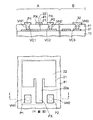
続いて、図7の断面図に示すように、膜厚測定領域Aにおいて、第1電極パッドP1、第2電極パッドP2及び第2金属層22のパッド部PXの上の部分の第2層間絶縁層42をレーザで加工する。図7の断面図の膜厚測定領域Aは図7の平面図のI−Iに沿った断面に相当する。図7の平面図は透視的に描かれている。
Subsequently, as shown in the cross-sectional view of FIG. 7, in the film thickness measurement region A, the second interlayer insulation of the portion of the first electrode pad P <b> 1, the second electrode pad P <b> 2, and the pad portion PX of the
これにより、図7の平面図を加えて参照すると、第2層間絶縁層42に、第1電極パッドP1、第2電極パッドP2及び第2金属層22のパッド部PXを一括して露出させる開口部42aが形成される。第2金属層22のパッド部PX以外の領域は、膜厚測定対象の第2層間絶縁層42によって被覆された状態となる。
Accordingly, referring to FIG. 7 in addition to the plan view, the first electrode pad P1, the second electrode pad P2, and the pad portion PX of the
このとき同時に、図7の断面図に示すように、配線形成領域Bでは、レーザ加工により、第2配線層32に到達する第4ビアホールVH4が第2層間絶縁層42に形成される。あるいは、後述する膜厚測定が終了してから配線形成領域Bに第4ビアホールVH4を形成してもよい。
At the same time, as shown in the cross-sectional view of FIG. 7, in the wiring formation region B, a fourth via hole VH4 reaching the
以上により、実施形態の膜厚測定機能付き基板1が得られる。
As described above, the
図7の断面図及び平面図に示すように、実施形態の膜厚測定機能付き基板1の膜厚測定領域Aでは、下地絶縁層10の上にパッチアンテナ用の第1金属層21が形成されている。第1金属層21はグランドプレーン層として形成される。
As shown in the sectional view and the plan view of FIG. 7, the
第1金属層21の上には第1層間絶縁層41が形成されている。さらに、第1金属層21に対向するように、第1層間絶縁層41の上にパッチアンテナ用の第2金属層22が形成されている。第2金属層22はアンテナパターン層として形成される。
A first
第1層間絶縁層41の上には、第1層間絶縁層41に配置された第1ビア導体VC1を介して第1金属層21の一端部に接続される第1電極パッドP1が形成されている。また、第1層間絶縁層41の上には、第1層間絶縁層41に配置された第2ビア導体VC2を介して第1金属層21の他端部に接続される第2電極パッドP2が形成されている。
A first electrode pad P1 connected to one end of the
第2金属層22は、第1、第2電極パッドP1,P2側に延びる延在部22aを有し、その先端側にパッド部PXを備える。第2金属層22のパッド部PXは、第1電極パッドP1と第2電極パッドP2の間の領域にそれらと横方向に並ぶように配置されている。
The
図8は図7の平面図のII−IIに沿った断面図である。図7の平面図及び図8に示すように、膜厚測定対象となる第2層間絶縁層42は第2金属層22のパッド部PXを除く全体を被覆して形成されている。
8 is a cross-sectional view taken along the line II-II of the plan view of FIG. As shown in the plan view of FIG. 7 and FIG. 8, the second
そして、図7の断面図及び平面図に示すように、膜厚測定対象となる第2層間絶縁層42は、第1電極パッドP1、第2電極パッドP2及び第2金属層22のパッド部PXを露出させる一括した開口部42aを備えている。あるいは、第1電極パッドP1、第2電極パッドP2及び第2金属層22のパッド部PXの上に開口部が分割されて個別に配置されてもいてもよい。
As shown in the cross-sectional view and the plan view of FIG. 7, the second
このようにして、膜厚測定領域Aに、第1層間絶縁層41が第1金属層21と第2金属層22とによって挟まれたキャパシタ構造からなるパッチアンテナPAが構築されている。後述するように、パッチアンテナPAが膜厚測定機能を有する。
In this manner, the patch antenna PA having a capacitor structure in which the first
パッチアンテナPAは、配線形成領域Bに形成された第1配線層31及び第2配線層32と電気的に独立して形成される。
The patch antenna PA is formed electrically independently from the
同じく図7の断面図に示すように、膜厚測定機能付き基板1の配線形成領域Bでは、下地絶縁層10の上に第1配線層31が形成されている。下地絶縁層10及び第1配線層31の上に第1層間絶縁層41が形成されている。第1層間絶縁層41の上には、第1層間絶縁層41に配置された第3ビア導体VC3を介して第1配線層31に接続される第2配線層32が形成されている。
Similarly, as shown in the sectional view of FIG. 7, the
また、第1層間絶縁層41の上には第2層間絶縁層42が形成されている。第2層間絶縁層42には第2配線層32に到達する第4ビアホールVH4が形成されている。この時点では、第4ビアホールVH4は必ずしも形成されている必要はない。
A second
膜厚測定領域Aの第1金属層21と配線形成領域Bの第1配線層31とは、同一層から形成され、電気的に絶縁されている。また同様に、膜厚測定領域Aの第2金属層22と配線形成領域Bの第2配線層32とは、同一層から形成され、電気的に絶縁されている。
The
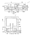
次に、図9及び図10を参照して、第2層間絶縁層42の膜厚測定方法について説明する。図9の断面図は図9の平面図のI−Iに沿った断面に相当する。図9の平面図は透視的に描かれている。また、図10は図9の平面図のII−IIに沿った断面図である。
Next, a method for measuring the thickness of the second
図9の断面図及び平面図に示すように、一つの信号ピンSと2つのグランドピンGを備えたGSG(グランド・信号・グランド)プローブ(不図示)を用意する。 As shown in the sectional view and plan view of FIG. 9, a GSG (ground / signal / ground) probe (not shown) having one signal pin S and two ground pins G is prepared.
そして、パッチアンテナPAの第2金属層22のパッド部PXにGSGプローブの信号ピンSを接触させて接続する。これと同時に、パッチアンテナPAの第1電極パッドP1及び第2電極パッドP2にGSGプローブのグランドピンGをそれぞれ接触させて接続する。
Then, the signal pin S of the GSG probe is brought into contact with and connected to the pad portion PX of the
これにより、GSGプローブの信号ピンSは、パッド部PXに繋がる第2金属層22に電気的に接続される。また、GSGプローブの2つのグランドピンGは第1、第2電極パッドP1,P2及び第1、第2ビア導体VC1,VC2を介して下側の第1金属層21にそれぞれ電気的に接続される。
Thereby, the signal pin S of the GSG probe is electrically connected to the
そして、GSGプローブに接続したネットワークアナライザ(不図示)を用いてパッチアンテナPAの共振周波数を測定する。共振周波数とは、パッチアンテナPAに高周波を印加し、高周波の周波数を徐々に変えたときに高周波電流が最大となる周波数である。 Then, the resonance frequency of the patch antenna PA is measured using a network analyzer (not shown) connected to the GSG probe. The resonance frequency is a frequency at which the high frequency current becomes maximum when a high frequency is applied to the patch antenna PA and the frequency of the high frequency is gradually changed.
パッチアンテナPAの上に形成された第2層間絶縁層42の膜厚が変化すると、パッチアンテナPAの共振周波数が変化する。
When the film thickness of the second
この特性を利用して、第2層間絶縁層42の膜厚とパッチアンテナPAの共振周波数との関係を検量線として予め作成しておく。そして、測定サンプルのパッチアンテナPAの共振周波数を測定することにより、第2層間絶縁層42の厚みを検量線のデータから算出することができる。
Using this characteristic, the relationship between the film thickness of the second
図10に示すように、パッチアンテナPAの端部に発生する電界は、第2金属層22の上面から第2層間絶縁層42、第1層間絶縁層41及び下地絶縁層10を通過し、第1金属層21の下面に向う。
As shown in FIG. 10, the electric field generated at the end of the patch antenna PA passes through the second
これにより、第2層間絶縁層42が存在しない場合に比べて、パッチアンテナPAが構築するキャパシタの容量が実質的に変化するため、それに基づいてパッチアンテナPAの共振周波数が変化するものと推測される。
Thereby, compared with the case where the second
本願発明者は、上記した図9で説明した膜厚測定方法により、パッチアンテナPAの上の第2層間絶縁層42の膜厚を変えた5つの実験サンプルを作成し、それぞれの実験サンプルの共振周波数を測定した。膜厚測定対象の絶縁層としてポリイミド層を使用し、膜厚は、0μm、63μm、126μm、189μm、252μmとした。
The inventor of the present application creates five experimental samples in which the film thickness of the second
また、パッチアンテナPAの第2金属層22の延在部22aを除く四角状領域の面積は1mm×1mm程度に設定した。
Further, the area of the square region excluding the extending
図11にその実験結果が示されおり、ポリイミド層の膜厚とパッチアンテナの共振周波数との関係がグラフ化されている。図11に示すように、ポリイミド層の厚みが0μmのときは共振周波数が65.91GHzであり、膜厚が63μmのときは共振周波数が63.32GHzに下がり、膜厚が126μmのときは共振周波数がさらに62.57GHzに下がった。 FIG. 11 shows the experimental results, and the relationship between the film thickness of the polyimide layer and the resonance frequency of the patch antenna is graphed. As shown in FIG. 11, when the thickness of the polyimide layer is 0 μm, the resonance frequency is 65.91 GHz, when the film thickness is 63 μm, the resonance frequency decreases to 63.32 GHz, and when the film thickness is 126 μm, the resonance frequency. Fell further to 62.57 GHz.
このように、ポリイミド層の膜厚が0μmから126μmまでの範囲では、膜厚が薄くなるにつれて共振周波数が低くなる特性となった。 Thus, when the film thickness of the polyimide layer is in the range from 0 μm to 126 μm, the resonance frequency becomes lower as the film thickness becomes thinner.
一方、ポリイミド層の膜厚を189μmにさらに厚くても共振周波数は62.55GHzで殆ど変化せず、さらにポリイミド層の膜厚を252μmに厚くしても共振周波数は62.53GHzで殆ど変化しなかった。 On the other hand, even if the thickness of the polyimide layer is further increased to 189 μm, the resonance frequency hardly changes at 62.55 GHz, and even when the thickness of the polyimide layer is increased to 252 μm, the resonance frequency hardly changes at 62.53 GHz. It was.
このように、ポリイミド層の厚みが126μmを超えると、共振周波数は変化しないことが分かった。これは、前述した図10での説明において、ポリイミド層の膜厚がある程度厚くなると、第2金属層22から上側に発生する電界がポリイミド層の膜みの途中までしか到達しなくなり、飽和状態となるためと推測される。
Thus, it was found that the resonance frequency did not change when the thickness of the polyimide layer exceeded 126 μm. In the description with reference to FIG. 10 described above, when the film thickness of the polyimide layer is increased to some extent, the electric field generated on the upper side from the
上記した実験サンプルのパッチアンテナPAでは、ポリイミド層の厚みが126μm以下であれば、パッチアンテナPAの共振周波数を測定することにより膜厚を算出することができる。配線基板で使用される層間絶縁層の膜厚は、10μm〜100μm、例えば30μm程度であるため、上記した方法によって膜厚測定を行うことができる。 In the patch antenna PA of the experimental sample described above, if the polyimide layer has a thickness of 126 μm or less, the film thickness can be calculated by measuring the resonance frequency of the patch antenna PA. Since the film thickness of the interlayer insulating layer used in the wiring board is 10 μm to 100 μm, for example, about 30 μm, the film thickness can be measured by the method described above.
このようにして、図11のように、膜厚測定対象の絶縁層の膜厚とパッチアンテナの共振周波数との関係を検量線として予め作成しておく。そして、測定サンプルのパッチアンテナの共振周波数を測定することにより、検量線のデータから絶縁層の膜厚を算出することができる。 In this way, as shown in FIG. 11, the relationship between the thickness of the insulating layer to be measured and the resonance frequency of the patch antenna is prepared in advance as a calibration curve. Then, by measuring the resonance frequency of the patch antenna of the measurement sample, the film thickness of the insulating layer can be calculated from the calibration curve data.
例えば、ある製品の測定サンプルにおいて、パッチアンテナPAの共振周波数が64.50GHzであったときは、図11の検量線から、パッチアンテナPAの上のポリイミド層の膜厚が30μm程度であることが算出される。 For example, in a measurement sample of a certain product, when the resonance frequency of the patch antenna PA is 64.50 GHz, the thickness of the polyimide layer on the patch antenna PA is about 30 μm from the calibration curve of FIG. Calculated.
図11のような検量線のデータをシステム化して、パッチアンテナPAの共振周波数の測定値とリンクさせることにより、共振周波数を測定と同時に膜厚を表示させることも可能である。 It is also possible to display the film thickness simultaneously with the measurement of the resonance frequency by systematizing the calibration curve data as shown in FIG. 11 and linking it with the measurement value of the resonance frequency of the patch antenna PA.
なお、パッチアンテナPAの第2金属層22(アンテナパターン層)の設計を変更することにより、共振周波数を変えることができる。各種の絶縁層の膜厚測定に対して、膜厚の変化に応じて共振周波数が変化するように、第2金属層22(アンテナパターン層)の設計を行えばよい。 Note that the resonance frequency can be changed by changing the design of the second metal layer 22 (antenna pattern layer) of the patch antenna PA. For the measurement of the thickness of various insulating layers, the second metal layer 22 (antenna pattern layer) may be designed so that the resonance frequency changes according to the change in thickness.
以上のように、本実施形態では、パッチアンテナの共振周波数を測定することで層間絶縁層の膜厚を求めることができる。このため、3次元測長システムを使用する場合と違って、層間絶縁層の樹脂材料や各工程のプロセス条件を変更しても、その都度測定条件を調整する必要がなく、簡易な方法で膜厚測定を行うことができる。 As described above, in this embodiment, the film thickness of the interlayer insulating layer can be obtained by measuring the resonance frequency of the patch antenna. For this reason, unlike the case of using a three-dimensional length measurement system, even if the resin material of the interlayer insulating layer and the process conditions of each process are changed, it is not necessary to adjust the measurement conditions each time, and the film can be formed by a simple method. Thickness measurement can be performed.
また、膜厚測定を行う際に、ビアホールを必要としないため、ビアホールの径が小さくなっても膜厚測定が不可となる問題は発生しない。 Further, since no via hole is required when measuring the film thickness, there is no problem that the film thickness cannot be measured even when the diameter of the via hole is reduced.
また、溶出法を使用する場合と違って、膜厚測定用に配線基板から個片サンプルを採取することなく、非破壊でかつ短手番で膜厚測定を行うことができる。 Further, unlike the case where the elution method is used, the film thickness can be measured in a non-destructive and short manner without taking individual samples from the wiring board for film thickness measurement.
以上の方法によって図7の第2層間絶縁層42の膜厚測定を行った後に、配線形成領域Bの第2層間絶縁層42の上に所望の多層配線層が形成される。多層配線層の膜厚測定対象の層間絶縁層の下にパッチアンテナを形成することにより、その層間絶縁層の膜厚を同様に測定することができる。
After the film thickness measurement of the second
(第2の実施の形態)
第2実施形態では、他の絶縁層としてOSP膜の膜厚測定方法について説明する。図12〜図14はOSP膜の膜厚測定方法を説明するための図である。
(Second Embodiment)
In the second embodiment, a method for measuring the thickness of an OSP film as another insulating layer will be described. 12 to 14 are diagrams for explaining a method of measuring the thickness of the OSP film.
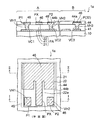
図12の断面図の膜厚測定領域Aは図12の平面図のI−Iに沿った断面に相当する。図12の平面図は透視的に描かれている。また、図13は図12の平面図のII−IIに沿った断面図である。 A film thickness measurement region A in the cross-sectional view of FIG. 12 corresponds to a cross section taken along II in the plan view of FIG. The plan view of FIG. 12 is drawn in perspective. FIG. 13 is a cross-sectional view taken along the line II-II of the plan view of FIG.
図12の断面図及び平面図に示すように、OSP膜の膜厚測定を行う場合は、前述した図4の工程において、配線形成領域Bでは第2配線層32が接続パッドPとして形成される。接続パッドPは、多層配線層の最上の配線層として形成され、島状に配置されてもよいし、あるいは引き出し配線の一端に配置されていてもよい。接続パッドPには、半導体素子などの電子部品が接続される。
As shown in the cross-sectional view and the plan view of FIG. 12, when measuring the thickness of the OSP film, the
そして、第1層間絶縁層41の上にソルダレジスト層44が形成される。配線形成領域Bでは、接続パッドPの上にソルダレジスト層44の第1開口部44aが配置される。また、膜厚測定領域Aでは、第2金属層22、第1、第2電極パッドP1,P2の上にソルダレジスト層44の第2開口部44bが一括して配置される。
Then, a solder resist
さらに、薬液処理によって、配線形成領域Bにおけるソルダレジスト層44の開口部44a内の接続パッドPの表面に薄膜のOSP膜46を形成する。このとき同時に、膜厚測定領域Aでは、ソルダレジスト層44の開口部44b内の第2金属層22、第1、第2電極パッドP1,P2にも同じ厚みのOSP膜46が形成される。図12の平面図の斜線ハッチング領域にOSP膜46が形成される。
Further, a
このようにして、図12及び図13の断面図に示すように、膜厚測定領域Aの第1、第1電極パッドP1,P2及び第2金属層22の上に膜厚測定対象となるOSP膜46が形成される。これにより、第2実施形態の膜厚測定機能付き基板1aが得られる。
In this way, as shown in the cross-sectional views of FIGS. 12 and 13, the OSP that is the target of film thickness measurement on the first and first
次いで、図14に示すように、前述した図9と同様に、パッチアンテナPAの第2金属層22のパッド部PXにGSGプローブの信号ピンSを接触させて接続する。また同時に、パッチアンテナPAの第1、第2電極パッドP1,P2にGSGプローブの2つのグランドピンGを接触させて接続する。
Next, as shown in FIG. 14, the signal pin S of the GSG probe is connected to and connected to the pad portion PX of the
このとき、第2金属層22のパッド部PX及び第1、第2電極パッドP1,P2の表面にOSP膜46が形成されている。しかし、GSGプローブの信号ピンS及びグランドピンGでOSP膜46を押し込んで突き破ることにより、第1、第2電極パッドP1,P2及びパッド部PXにGSGプローブを電気的に接続することができる。
At this time, the
そして同様に、OSP膜46で被覆されたパッチアンテナPAの共振周波数を測定する。前述した第1実施形態と同様に、OSP膜46の膜厚とパッチアンテナPAの共振周波数との関係を検量線として予め作成しておくことで、測定された共振周波数及び検量線のデータからOSP膜46の膜厚を算出することができる。第2実施形態は第1実施形態と同様な効果を奏する。
Similarly, the resonance frequency of the patch antenna PA covered with the
前述した第1、第2実施形態では、樹脂層及びOSP膜の膜厚測定を例示したが、各種の有機又は無機の絶縁層の膜厚を測定することができる。無機の絶縁層としては、シリコン酸化層、シリコン窒化層、又はシリコン酸化窒化層などがある。 In the first and second embodiments described above, the measurement of the film thickness of the resin layer and the OSP film is exemplified, but the film thickness of various organic or inorganic insulating layers can be measured. Examples of the inorganic insulating layer include a silicon oxide layer, a silicon nitride layer, and a silicon oxynitride layer.
1,1a…膜厚測定機能付き基板、10…下地絶縁層、12…シード層、13…めっきレジスト層、13a,42a…開口部、14…金属めっき層、21…第1金属層、22…第2金属層、31…第1配線層、32…第2配線層、41…第1層間絶縁層、42…第2層間絶縁層、44…ソルダレジスト層、44a…第1開口部、44b…第2開口部、46…OSP膜、A…膜厚測定領域、B…配線形成領域、G…グランドピン、PA…パッチアンテナ、P1…第1電極パッド、P2…第2電極パッド、PX…パッド部、S…信号ピン、VC1…第1ビア導体、VC2…第2ビア導体、VC3…第3ビア導体、VH1…第1ビアホール、VH2…第2ビアホール、VH3…第3ビアホール、VH4…第4ビアホール。
DESCRIPTION OF
Claims (10)
前記膜厚測定領域の前記下地絶縁層の上に形成されたアンテナ用の第1金属層と、
前記配線形成領域の前記下地絶縁層の上に形成された第1配線層と、
前記下地絶縁層、前記第1金属層及び前記第1配線層の上に形成された第1絶縁層と、
前記第1金属層と対向するように、前記膜厚測定領域の前記第1絶縁層の上に形成された、パッド部を有する前記アンテナ用の第2金属層と、
前記膜厚測定領域の前記第1絶縁層の上に形成され、前記第1絶縁層に配置された第1ビア導体を介して前記第1金属層に接続された第1電極パッドと、
前記配線形成領域の前記第1絶縁層の上に形成された第2配線層と、
前記第2金属層を被覆して形成され、膜厚測定対象となる第2絶縁層と
を有し、
前記第1金属層と前記第1配線層とは、同一層から形成されると共に、電気的に絶縁されており、
前記第2金属層と前記第2配線層とは、同一層から形成されると共に、電気的に絶縁されており、
前記パッド部と前記第1電極パッドとは、測定器のプローブが接続されるパッドであることを特徴とする膜厚測定機能付き基板。 A base insulating layer in which a film thickness measurement region and a wiring formation region are defined;
A first metal layer for an antenna formed on the base insulating layer in the film thickness measurement region;
A first wiring layer formed on the base insulating layer in the wiring formation region;
A first insulating layer formed on the base insulating layer, the first metal layer, and the first wiring layer;
A second metal layer for the antenna having a pad portion formed on the first insulating layer in the film thickness measurement region so as to face the first metal layer;
A first electrode pad formed on the first insulating layer in the film thickness measurement region and connected to the first metal layer via a first via conductor disposed in the first insulating layer;
A second wiring layer formed on the first insulating layer in the wiring formation region;
A second insulating layer that is formed to cover the second metal layer and is a thickness measurement target;
The first metal layer and the first wiring layer are formed from the same layer and are electrically insulated,
The second metal layer and the second wiring layer are formed from the same layer and are electrically insulated,
The substrate with a film thickness measuring function, wherein the pad portion and the first electrode pad are pads to which a probe of a measuring instrument is connected.
前記第2電極パッドは測定器のプローブが接続されるパッドであることを特徴とする請求項1に記載の膜厚測定機能付き基板。 A second electrode pad formed on the first insulating layer in the film thickness measurement region and connected to the first metal layer via a second via conductor disposed in the first insulating layer;
The substrate with a film thickness measuring function according to claim 1, wherein the second electrode pad is a pad to which a probe of a measuring instrument is connected.
前記第1金属層の上に形成された第1絶縁層と、
前記第1金属層に対向するように、前記第1絶縁層の上に形成された、パッド部を有する第2金属層と、
前記第1絶縁層の上に形成され、前記第1絶縁層に配置された第1ビア導体を介して前記第1金属層に接続される第1電極パッドと
を備えたアンテナを含む基板を用意する工程と、
前記第2金属層の上に、膜厚測定対象となる第2絶縁層を形成する工程と、
前記第1電極パッド及び前記パッド部に測定器のプローブを接続して、前記アンテナの共振周波数を測定する工程と、
前記共振周波数に基づいて、前記第2絶縁層の膜厚を算出する工程と
を有することを特徴する絶縁層の膜厚測定方法。 A first metal layer;
A first insulating layer formed on the first metal layer;
A second metal layer having a pad portion formed on the first insulating layer so as to face the first metal layer;
A substrate including an antenna is provided that includes a first electrode pad formed on the first insulating layer and connected to the first metal layer via a first via conductor disposed on the first insulating layer. And a process of
Forming a second insulating layer to be a film thickness measurement target on the second metal layer;
Connecting a probe of a measuring instrument to the first electrode pad and the pad part, and measuring a resonance frequency of the antenna;
A method of calculating a film thickness of the second insulating layer based on the resonance frequency.
前記アンテナの共振周波数を測定する工程では、前記開口部に露出する前記第1電極パッド及び前記パッド部に前記プローブを接続することを特徴とする請求項5に記載の絶縁層の膜厚測定方法。 In the step of forming the second insulating layer, after forming the second insulating layer covering the second metal layer and the first electrode pad, the opening for exposing the first electrode pad and the pad portion is formed in the opening portion. Forming a second insulating layer;
6. The method for measuring a thickness of an insulating layer according to claim 5, wherein in the step of measuring the resonance frequency of the antenna, the probe is connected to the first electrode pad exposed to the opening and the pad. .
前記アンテナの共振周波数を測定する工程では、前記第2絶縁層を前記プローブで突き破って前記第1電極パッド及び前記パッド部に前記プローブを接続することを特徴とする請求項5に記載の絶縁層の膜厚測定方法。 The step of forming the second insulating layer includes a step of forming a second insulating layer that covers the second metal layer and the first electrode pad,
6. The insulating layer according to claim 5, wherein in the step of measuring the resonance frequency of the antenna, the probe is connected to the first electrode pad and the pad portion by breaking through the second insulating layer with the probe. Film thickness measurement method.
前記アンテナの共振周波数を測定する工程では、前記第2電極パッドにも前記プローブを接続することを特徴とする請求項5乃至8のいずれか一項に記載の絶縁層の膜厚測定方法。 The antenna includes a second electrode pad formed on the first insulating layer and connected to the first metal layer through a second via conductor disposed in the first insulating layer.
The method for measuring a thickness of an insulating layer according to claim 5, wherein in the step of measuring the resonance frequency of the antenna, the probe is also connected to the second electrode pad.
Priority Applications (1)
| Application Number | Priority Date | Filing Date | Title |
|---|---|---|---|
| JP2014141569A JP6276658B2 (en) | 2014-07-09 | 2014-07-09 | Substrate with film thickness measuring function and method for measuring film thickness of insulating layer |
Applications Claiming Priority (1)
| Application Number | Priority Date | Filing Date | Title |
|---|---|---|---|
| JP2014141569A JP6276658B2 (en) | 2014-07-09 | 2014-07-09 | Substrate with film thickness measuring function and method for measuring film thickness of insulating layer |
Publications (3)
| Publication Number | Publication Date |
|---|---|
| JP2016017882A JP2016017882A (en) | 2016-02-01 |
| JP2016017882A5 JP2016017882A5 (en) | 2017-04-20 |
| JP6276658B2 true JP6276658B2 (en) | 2018-02-07 |
Family
ID=55233189
Family Applications (1)
| Application Number | Title | Priority Date | Filing Date |
|---|---|---|---|
| JP2014141569A Active JP6276658B2 (en) | 2014-07-09 | 2014-07-09 | Substrate with film thickness measuring function and method for measuring film thickness of insulating layer |
Country Status (1)
| Country | Link |
|---|---|
| JP (1) | JP6276658B2 (en) |
Families Citing this family (10)
| Publication number | Priority date | Publication date | Assignee | Title |
|---|---|---|---|---|
| JP6793103B2 (en) | 2017-09-29 | 2020-12-02 | ミネベアミツミ株式会社 | Strain gauge |
| CN111406196B (en) * | 2017-09-29 | 2022-03-29 | 美蓓亚三美株式会社 | Strain gauge |
| JP2019066312A (en) | 2017-09-29 | 2019-04-25 | ミネベアミツミ株式会社 | Strain gauge |
| JP2019066454A (en) | 2017-09-29 | 2019-04-25 | ミネベアミツミ株式会社 | Strain gauge and sensor module |
| JP2019066453A (en) * | 2017-09-29 | 2019-04-25 | ミネベアミツミ株式会社 | Strain gauge |
| JP2019082424A (en) | 2017-10-31 | 2019-05-30 | ミネベアミツミ株式会社 | Strain gauge |
| JP2019113411A (en) | 2017-12-22 | 2019-07-11 | ミネベアミツミ株式会社 | Strain gauge and sensor module |
| JP2019184344A (en) | 2018-04-05 | 2019-10-24 | ミネベアミツミ株式会社 | Strain gauge and manufacturing method therefor |
| WO2020085247A1 (en) | 2018-10-23 | 2020-04-30 | ミネベアミツミ株式会社 | Accelerator pedal, steering apparatus, 6-axis sensor, engine, bumper, and the like |
| JP7263220B2 (en) * | 2019-11-29 | 2023-04-24 | 新光電気工業株式会社 | Method for estimating film thickness of silane coupling coating |
Family Cites Families (2)
| Publication number | Priority date | Publication date | Assignee | Title |
|---|---|---|---|---|
| JP2007107976A (en) * | 2005-10-13 | 2007-04-26 | Canon Inc | Paper kind discrimination device |
| CN101583866B (en) * | 2006-11-21 | 2016-11-09 | 通用电气医疗集团生物科学公司 | Assemble in a reservoir and utilize RFID sensor |
-
2014
- 2014-07-09 JP JP2014141569A patent/JP6276658B2/en active Active
Also Published As
| Publication number | Publication date |
|---|---|
| JP2016017882A (en) | 2016-02-01 |
Similar Documents
| Publication | Publication Date | Title |
|---|---|---|
| JP6276658B2 (en) | Substrate with film thickness measuring function and method for measuring film thickness of insulating layer | |
| JP6996976B2 (en) | High speed interconnect for printed circuit boards | |
| WO2017094368A1 (en) | Multipoint-measurement strain sensor and production method for same | |
| JP5798435B2 (en) | Wiring board for electronic component inspection apparatus and manufacturing method thereof | |
| JP5424675B2 (en) | Semiconductor device manufacturing method and semiconductor device | |
| US20170047230A1 (en) | Fabrication method of packaging substrate | |
| JP2008160051A (en) | Printed circuit board that can identify manufacturing information | |
| US9629250B2 (en) | Method of manufacturing glass component, glass component, and glass interposer | |
| KR101136396B1 (en) | PCB within cavity and Fabricaring method of the same | |
| JP5777997B2 (en) | Wiring board for electronic component inspection apparatus and manufacturing method thereof | |
| US20180139840A1 (en) | Fabrication method of substrate structure | |
| US9236336B2 (en) | Systems and methods for mitigation of mechanical degradation in high performance electrical circuit packages | |
| JP5774332B2 (en) | Ceramic substrate for probe card and manufacturing method thereof | |
| JP6100617B2 (en) | Multi-layer wiring board and probe card board | |
| JP2012198190A5 (en) | ||
| JP2006344847A (en) | Substrate with built-in component, module equipped with built-in component using same, and method of manufacturing same | |
| JP6258810B2 (en) | Wiring board manufacturing method | |
| JP7049975B2 (en) | Wiring board and wiring board inspection method | |
| KR20120076266A (en) | Ceramic substrate for probe card and fabricating method thereof | |
| JP2011061490A (en) | Antenna element and antenna element inspection method | |
| TWI558284B (en) | Circuit board element and method for manufacturing the same | |
| KR20120137300A (en) | Method of manufacturing multilayer wiring substrate, and multilayer wiring substrate | |
| TWI470652B (en) | Slice resistor and manufacturing method therof | |
| JP7192423B2 (en) | Plating thickness determination method and multilayer wiring board manufacturing method | |
| KR101101552B1 (en) | Repairing method of ceramic substrate and repaired ceramic substrate using the same |
Legal Events
| Date | Code | Title | Description |
|---|---|---|---|
| A521 | Written amendment |
Free format text: JAPANESE INTERMEDIATE CODE: A523 Effective date: 20170316 |
|
| A621 | Written request for application examination |
Free format text: JAPANESE INTERMEDIATE CODE: A621 Effective date: 20170316 |
|
| A977 | Report on retrieval |
Free format text: JAPANESE INTERMEDIATE CODE: A971007 Effective date: 20171213 |
|
| TRDD | Decision of grant or rejection written | ||
| A01 | Written decision to grant a patent or to grant a registration (utility model) |
Free format text: JAPANESE INTERMEDIATE CODE: A01 Effective date: 20171226 |
|
| A61 | First payment of annual fees (during grant procedure) |
Free format text: JAPANESE INTERMEDIATE CODE: A61 Effective date: 20180112 |
|
| R150 | Certificate of patent or registration of utility model |
Ref document number: 6276658 Country of ref document: JP Free format text: JAPANESE INTERMEDIATE CODE: R150 |