KR101101552B1 - Repair method of ceramic substrate and repaired ceramic substrate using the same - Google Patents
Repair method of ceramic substrate and repaired ceramic substrate using the same Download PDFInfo
- Publication number
- KR101101552B1 KR101101552B1 KR1020090085932A KR20090085932A KR101101552B1 KR 101101552 B1 KR101101552 B1 KR 101101552B1 KR 1020090085932 A KR1020090085932 A KR 1020090085932A KR 20090085932 A KR20090085932 A KR 20090085932A KR 101101552 B1 KR101101552 B1 KR 101101552B1
- Authority
- KR
- South Korea
- Prior art keywords
- wiring
- repair
- ceramic substrate
- main wiring
- pattern
- Prior art date
- Legal status (The legal status is an assumption and is not a legal conclusion. Google has not performed a legal analysis and makes no representation as to the accuracy of the status listed.)
- Expired - Fee Related
Links
Images


Classifications
-
- H—ELECTRICITY
- H05—ELECTRIC TECHNIQUES NOT OTHERWISE PROVIDED FOR
- H05K—PRINTED CIRCUITS; CASINGS OR CONSTRUCTIONAL DETAILS OF ELECTRIC APPARATUS; MANUFACTURE OF ASSEMBLAGES OF ELECTRICAL COMPONENTS
- H05K3/00—Apparatus or processes for manufacturing printed circuits
- H05K3/22—Secondary treatment of printed circuits
- H05K3/225—Correcting or repairing of printed circuits
-
- H—ELECTRICITY
- H05—ELECTRIC TECHNIQUES NOT OTHERWISE PROVIDED FOR
- H05K—PRINTED CIRCUITS; CASINGS OR CONSTRUCTIONAL DETAILS OF ELECTRIC APPARATUS; MANUFACTURE OF ASSEMBLAGES OF ELECTRICAL COMPONENTS
- H05K1/00—Printed circuits
- H05K1/02—Details
- H05K1/03—Use of materials for the substrate
- H05K1/0306—Inorganic insulating substrates, e.g. ceramic, glass
Landscapes
- Engineering & Computer Science (AREA)
- Microelectronics & Electronic Packaging (AREA)
- Chemical & Material Sciences (AREA)
- Ceramic Engineering (AREA)
- Inorganic Chemistry (AREA)
- Manufacturing & Machinery (AREA)
- Manufacturing Of Printed Wiring (AREA)
- Production Of Multi-Layered Print Wiring Board (AREA)
Abstract
본 발명은 적어도 하나의 메인 배선 및 상기 메인 배선 중 손상된 메인 배선을 리페어하는 적어도 하나의 리페어 배선을 구비한 세라믹층을 마련하는 단계, 상기 세라믹층에 상기 메인 배선과 상기 리페어 배선이 각각 전기적 접속 가능하도록 제1 도전 패턴을 형성하는 단계, 상기 메인 배선의 손상 발생시, 상기 제1 도전 패턴을 제거하는 단계, 상기 도전 패턴이 제거된 상기 손상된 메인 배선 상에 절연 부재를 형성하는 단계, 상기 세라믹층에 상기 손상된 메인 배선과 상기 리페어 배선을 연결하도록 리페어 패턴을 형성하는 단계 및 상기 리페어 패턴이 형성된 부분을 제외한 상기 메인 배선 및 상기 리페어 배선 상에 제2 도전 패턴을 형성하는 단계를 포함하는 세라믹 기판의 리페어 방법 및 이를 이용하여 리페어된 세라믹기판을 제공한다.The present invention provides a ceramic layer having at least one main wiring and at least one repair wiring for repairing a damaged main wiring among the main wirings, wherein the main wiring and the repair wiring are electrically connected to the ceramic layer, respectively. Forming a first conductive pattern so as to remove the first conductive pattern when the main wiring is damaged; forming an insulating member on the damaged main wiring from which the conductive pattern has been removed; Forming a repair pattern to connect the damaged main wiring to the repair wiring; and forming a second conductive pattern on the main wiring and the repair wiring except for a portion where the repair pattern is formed. It provides a method and repaired ceramic substrate using the same.
본 발명의 실시예에 따르면, 불량 발생시 간단한 공정으로 리페어가 가능하며 제조 비용을 저감할 수 있는 세라믹 기판의 리페어 방법 및 이를 이용하여 리페어된 세라믹 기판을 제공할 수 있다.According to an exemplary embodiment of the present invention, a repair process can be performed in a simple process when a defect occurs and a manufacturing method of a ceramic substrate capable of reducing manufacturing costs and a repaired ceramic substrate using the same can be provided.
세라믹 기판, 리페어, 전기적 불량 Ceramic Board, Repair, Electrical Defect
Description
본 발명은 불량 발생시 간단한 공정으로 리페어가 가능하며 제조 비용을 저감할 수 있는 세라믹 기판의 리페어 방법 및 이를 이용하여 리페어된 세라믹 기판에 관한 것이다.The present invention relates to a method of repairing a ceramic substrate that can be repaired in a simple process when a defect occurs and to reduce manufacturing costs, and to a ceramic substrate repaired using the same.
최근 제품의 고집적화 및 소형화 추세에 의하여 작은 면적에 많은 기능을 가진 기판이 요구되고 있다.Recently, due to the trend of high integration and miniaturization of products, a substrate having many functions in a small area is required.
이러한 추세에 부응하기 위하여 전기적인 특성을 가지는 제품은 신호선의 두께를 점점 더 미세하게 고안하고 제작하게 된다.In order to cope with this trend, products with electrical characteristics are designed and manufactured with a finer thickness of signal lines.
이러한 경우, 공정의 수준이 높아지게 되고 이로 인하여 공정 수율이 나빠지게 된다. 특히 여러 개의 기능을 개별 회로 배선 기판에 사용하던 것이 현재는 소형화를 위하여 하나의 회로 배선 기판에 모두 집적하게 되고 따라서 그 회로 기판 에 사용되는 배선들의 밀도가 높아지게 된다. 이로 인하여 실제 연결되어야 할 네트(net)나 패스(path)가 기하 급수적으로 늘어나게 되고, 이러한 패스 중에 하나라도 불량이 발생하게 되는 경우에는 해당 기판은 폐기된다.In this case, the level of the process will be high, resulting in poor process yield. In particular, the use of several functions in separate circuit wiring boards is now integrated in one circuit wiring board for miniaturization, and thus the density of wirings used in the circuit board becomes high. As a result, the net or path to be actually connected increases exponentially, and if any one of these passes fails, the substrate is discarded.
또한, 회로 배선 기판(PCB, LTCC, HTCC 및 세라믹 회로 배선 기판 등)의 제작시 기판 제작 후 소자의 패키징이나 혹은 다른 후공정을 하기 전에 기판의 양불 검사를 실시한다. 이 경우, 보통은 전기적인 신호의 흐름을 만드는 네트나 패스 등의 오픈(open) 불량 또는 쇼트(short) 불량 테스트를 실시하게 된다.In addition, when fabricating a circuit wiring board (PCB, LTCC, HTCC, ceramic circuit wiring board, etc.), the board is inspected before and after the fabrication of the substrate and before the device is packaged or another post-process. In this case, open or short failure tests, such as nets or paths, which usually make electrical signal flows, are performed.
하지만, 이미 열을 가하여 소성한 제품은 불량이 발생할 경우 불량이 발생한 특정 네트나 패스에 대하여 리페어하기는 매우 어렵다. 따라서, 보통의 경우에는 불량이 발생한 기판은 폐기 처리하고 다시 제작을 한다.However, products that have already been heated and fired are very difficult to repair for a particular net or path where the failure occurred. Therefore, in a normal case, the board | substrate which a defect generate | occur | produce is discarded and manufactured again.
특히, 기판 내층에서 특정 네트 연결되면 안돼는 다른 네트와 쇼트 불량이 발생한 결과가 검출되었을 때는 리페어가 어려우며 제품을 폐기해야 한다.In particular, it is difficult to repair and dispose of the product when a result of a short defect with another net that should not be connected to a specific net in the board layer is detected.
본 발명은 상기와 같은 문제점을 해결하기 위한 것으로, 본 발명의 목적은 불량 발생시 간단한 공정으로 리페어가 가능하며 제조 비용을 저감할 수 있는 세라믹 기판의 리페어 방법 및 이를 이용하여 리페어된 세라믹 기판을 제공하는 것이다.The present invention is to solve the above problems, an object of the present invention is to provide a repair method of a ceramic substrate that can be repaired in a simple process when the failure occurs and to reduce the manufacturing cost and a repaired ceramic substrate using the same will be.
상기한 목적을 달성하기 위해서, 본 발명의 일 실시 형태는,In order to achieve the above object, one embodiment of the present invention,
적어도 하나의 메인 배선 및 상기 메인 배선 중 손상된 메인 배선을 리페어하는 적어도 하나의 리페어 배선을 구비한 세라믹층을 마련하는 단계, 상기 세라믹층에 상기 메인 배선과 상기 리페어 배선이 각각 전기적 접속 가능하도록 제1 도전 패턴을 형성하는 단계, 상기 메인 배선의 손상 발생시, 상기 제1 도전 패턴을 제거하는 단계, 상기 도전 패턴이 제거된 상기 손상된 메인 배선 상에 절연 부재를 형성하는 단계, 상기 세라믹층에 상기 손상된 메인 배선 상에 형성된 절연 부재와 상기 리페어 배선을 연결하도록 리페어 패턴을 형성하는 단계 및 상기 리페어 패턴이 형성된 부분을 제외한 상기 메인 배선 및 상기 리페어 배선 상에 제2 도전 패턴을 형성하는 단계를 포함하는 세라믹 기판의 리페어 방법 및 이를 이용하여 리페어된 세라믹기판을 제공한다.Providing a ceramic layer having at least one main wiring and at least one repair wiring for repairing a damaged main wiring among the main wirings, wherein the first wiring and the repair wiring are electrically connected to the ceramic layer, respectively; Forming a conductive pattern, removing the first conductive pattern when the damage occurs in the main wiring, forming an insulating member on the damaged main wiring from which the conductive pattern has been removed, and damaging the main in the ceramic layer. Forming a repair pattern to connect the insulating member formed on the wiring to the repair wiring; and forming a second conductive pattern on the main wiring and the repair wiring except for a portion where the repair pattern is formed. Repair method and a repaired ceramic substrate using the same All.
여기서, 전기적 불량 발생시, 상기 손상된 메인 배선에 전달되는 전기적 신호는 상기 리페어 패턴을 통하여 상기 리페어 배선에 전달되도록 리페어될 수 있다.Here, when an electrical failure occurs, the electrical signal transmitted to the damaged main wiring may be repaired to be transmitted to the repair wiring through the repair pattern.
여기서, 상기 도전 패턴을 제거하는 단계는, 상기 도전 패턴을 연마하여 상기 손상된 메인 배선을 노출시키는 단계 및 상기 노출된 메인 배선의 일부 영역을 제거하여 홈부를 형성하는 단계로 포함할 수 있다.The removing of the conductive pattern may include polishing the conductive pattern to expose the damaged main wiring and removing a portion of the exposed main wiring to form a groove.
그리고, 상기 홈부는 레이저 식각, 화학적 식각, 펀칭 또는 레이저 드릴링 중 적어도 하나의 방법에 의해 형성될 수 있다.The groove may be formed by at least one of laser etching, chemical etching, punching, or laser drilling.
또한, 상기 절연 부재는 유전체로 구성된 페이스트로 형성될 수 있다.In addition, the insulating member may be formed of a paste made of a dielectric.
그리고, 상기 도전 패턴 및 상기 리페어 패턴은 스크린 프린팅, 포토 리소그래피, 증착, 도금 또는 화학적 식각 중 적어도 하나의 방법에 의해 형성될 수 있다.The conductive pattern and the repair pattern may be formed by at least one method of screen printing, photolithography, deposition, plating, or chemical etching.
여기서, 상기 도전 패턴 및 상기 리페어 패턴은 상기 도전 패턴 및 상기 리페어 패턴은 은과 상기 은을 도금하는 금, 구리, 구리 합금, 금, 금 합금, 텅스텐 및 텅스텐 합금 중 적어도 어느 하나의 재질로 형성될 수 있다.The conductive pattern and the repair pattern may be formed of at least one of gold, copper, a copper alloy, gold, a gold alloy, tungsten and a tungsten alloy to plate silver and the silver. Can be.
또한, 상기 세라믹 기판의 내부 또는 외부에 접지용 배선을 형성하는 단계를 더 포함할 수 있다.In addition, the method may further include forming a grounding wire inside or outside the ceramic substrate.
여기서, 상기 세라믹 기판의 내부 또는 외부에 접지용 배선을 형성하는 단계를 더 포함할 수 있다.Here, the method may further include forming a grounding wire inside or outside the ceramic substrate.
또한, 상기 세라믹 기판의 내부 또는 외부에 테스트용 배선을 형성하는 단계를 더 포함할 수 있다.The method may further include forming test wirings inside or outside the ceramic substrate.
여기서, 전기적 테스트시, 상기 리페어 배선은 상기 테스트용 배선에 연결될 수 있다.Here, during the electrical test, the repair wiring may be connected to the test wiring.
상기한 목적을 달성하기 위해서, 본 발명의 다른 실시 형태는,In order to achieve the above object, another embodiment of the present invention,
적어도 하나의 메인 배선을 구비한 세라믹층, 상기 메인 배선과 전기적 접속이 가능하도록 상기 세라믹층에 형성된 도전 패턴, 상기 세라믹층에 형성되며, 상기 메인 배선 중 손상된 메인 배선을 리페어하는 적어도 하나의 리페어 배선, 상기 손상된 메인 배선과 상기 도전 패턴을 절연하는 절연 부재 및 상기 세라믹층에 형성되며, 상기 손상된 메인 배선 상에 형성된 절연 부재와 상기 리페어 배선을 연결하는 리페어 패턴을 포함하는 세라믹 기판을 제공한다.A ceramic layer having at least one main wiring, a conductive pattern formed in the ceramic layer to be electrically connected to the main wiring, and at least one repair wiring formed in the ceramic layer and repairing a damaged main wiring among the main wirings The present invention provides a ceramic substrate including an insulating member for insulating the damaged main wiring and the conductive pattern, and a repair pattern formed on the ceramic layer and connecting the insulating member formed on the damaged main wiring and the repair wiring.
여기서, 전기적 불량 발생시, 상기 손상된 메인 배선에 전달되는 전기적 신호는 상기 리페어 패턴을 통하여 상기 리페어 배선에 전달되도록 리페어될 수 있다.Here, when an electrical failure occurs, the electrical signal transmitted to the damaged main wiring may be repaired to be transmitted to the repair wiring through the repair pattern.
여기서, 상기 절연 부재는 유전체로 구성된 페이스트로 이루어질 수 있다.Here, the insulating member may be made of a paste composed of a dielectric.
또한, 상기 도전 패턴 및 상기 리페어 패턴은 상기 도전 패턴 및 상기 리페어 패턴은 은과 상기 은을 도금하는 금, 구리, 구리 합금, 금, 금 합금, 텅스텐 및 텅스텐 합금 중 적어도 어느 하나의 재질로 이루어질 수 있다.The conductive pattern and the repair pattern may be made of at least one of gold, copper, copper alloy, gold, gold alloy, tungsten and tungsten alloy to plate the silver and the silver. have.
여기서, 상기 세라믹 기판의 내부 또는 외부에 접지용 배선을 더 포함할 수 있다.Here, the wiring for grounding may be further included inside or outside the ceramic substrate.
여기서, 상기 세라믹 기판의 내부 또는 외부에 테스트용 배선을 더 포함할 수 있다.Here, the test wiring may be further included inside or outside the ceramic substrate.
본 발명에 따르면, 불량 발생시 간단한 공정으로 리페어가 가능하며 제조 비용을 저감할 수 있는 세라믹 기판의 리페어 방법 및 이를 이용하여 리페어된 세라믹 기판을 제공할 수 있다. According to the present invention, it is possible to provide a repairing method of a ceramic substrate which can be repaired in a simple process when a defect occurs and to reduce manufacturing costs, and to provide a repaired ceramic substrate using the same.
또한, 리페어 배선과 접지용 배선을 연결함으로써 신호선 간에 발생할 수 있는 크로스-토크(cross-talk)를 방지하는 쉴딩(shielding) 기능을 할 수 있어 세라믹 기판의 전기적 특성을 더욱 양호하게 할 수 있다.In addition, by connecting the repair wiring and the ground wiring, it is possible to perform a shielding function to prevent cross-talk that may occur between signal lines, thereby making it possible to improve the electrical characteristics of the ceramic substrate.
이하, 첨부된 도면을 참조하여 본 발명의 바람직한 실시형태들을 설명한다.Hereinafter, preferred embodiments of the present invention will be described with reference to the accompanying drawings.
그러나, 본 발명의 실시형태는 여러 가지 다른 형태로 변형될 수 있으며, 본 발명의 범위가 이하 설명하는 실시 형태로 한정되는 것은 아니다. 또한, 본 발명의 실시형태는 당업계에서 평균적인 지식을 가진 자에게 본 발명을 더욱 완전하게 설명하기 위해서 제공되는 것이다. 따라서, 도면에서의 요소들의 형상 및 크기 등은 보다 명확한 설명을 위해 과장될 수 있으며, 도면상의 동일한 부호로 표시되는 요소는 동일한 요소이다.However, embodiments of the present invention may be modified in various other forms, and the scope of the present invention is not limited to the embodiments described below. In addition, the embodiments of the present invention are provided to more completely explain the present invention to those skilled in the art. Accordingly, the shape and size of elements in the drawings may be exaggerated for clarity, and the elements denoted by the same reference numerals in the drawings are the same elements.
이하에서는 도 1 내지 도 2d를 참조하여 본 발명의 실시예에 따른 세라믹 기판의 형성 공정을 설명한다.Hereinafter, a process of forming a ceramic substrate according to an embodiment of the present invention will be described with reference to FIGS. 1 to 2D.
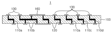
도 1은 본 발명의 실시예에 따라 제조된 세라믹 기판을 개략적으로 나타내는 단면도이고, 도 2a 내지 도 2d는 본 발명의 실시예에 따른 세라믹 기판을 리페어하는 공정을 개략적으로 나타내는 단면도이다.1 is a cross-sectional view schematically illustrating a ceramic substrate manufactured according to an embodiment of the present invention, and FIGS. 2A to 2D are cross-sectional views schematically illustrating a process of repairing a ceramic substrate according to an embodiment of the present invention.
본 발명의 실시예에 따른 세라믹 기판(1)은 적어도 하나의 메인 배선(110a, 110b, 110c, 110d)을 구비한 세라믹층(100), 상기 메인 배선(110a, 110b, 110c, 110d)과 전기적 접속이 가능하도록 상기 세라믹층(100)에 형성된 도전 패턴(130), 상기 세라믹층(100)에 형성되며, 상기 메인 배선(110a, 110b, 110c, 110d) 중 손상된 메인 배선(110b)을 리페어하는 적어도 하나의 리페어 배선(120), 상기 손상된 메인 배선(110b)과 상기 도전 패턴(130)을 절연하는 절연 부재(150) 및 상기 세라믹층(100)에 형성되며, 상기 손상된 메인 배선(110b)과 상기 리페어 배선(120)을 연결하는 리페어 패턴(160)을 포함한다.The
여기서, 세라믹 기판(1)에 전기적 불량이 발생하는 경우, 상기 손상된 메인 배선(110b)에 전달되는 전기적 신호는 상기 리페어 패턴(160)을 통하여 상기 리페어 배선(120)에 전달됨으로써 상기 세라믹 기판(1)이 리페어될 수 있다.Here, when an electrical failure occurs in the
이때, 상기 손상된 메인 배선(110b)과 상기 도전 패턴(130)을 절연하는 절연 부재(150)는 유전체로 구성된 페이스트로 이루어질 수 있다.In this case, the
그리고, 상기 도전 패턴(130) 및 상기 리페어 패턴(160)은 은과 상기 은을 도금하는 금, 구리, 구리 합금, 금, 금 합금, 텅스텐 및 텅스텐 합금 중 적어도 어느 하나의 재질로 이루어는 것이 바람직하지만, 상기 도전 패턴(130) 및 상기 리페 어 패턴(160)을 이루는 물질은 이에 한정되지 않으며, 전도성이 좋은 금속 또는 합금으로 이루어질 수 있다. 여기서, 상기 도전 패턴(130) 및 상기 리페어 패턴(160)이 은과 상기 은을 도금하는 금으로 구성되는 경우에는 은이 산화될 수 있으므로, 은 위에 금으로 도금을 하여 은의 산화를 방지할 수 있다.The
또한, 세라믹 기판(1)은 내부 또는 외부에 접지용 배선(110d)과 테스트용 배선(110c)을 더 포함할 수 있다.In addition, the
이하, 본 발명의 실시예에 따른 세라믹 기판의 리페어 방법에 대해 상세하게 설명한다.Hereinafter, the repair method of the ceramic substrate according to the embodiment of the present invention will be described in detail.
도 2a를 참조하면, 적어도 하나의 메인 배선(110a, 110b, 110c, 110d) 및 상기 메인 배선(110a, 110b, 110c, 110d) 중 손상된 메인 배선(110b)을 리페어할 수 있는 적어도 하나의 리페어 배선(120)을 구비한 세라믹층(100)을 마련한다. 여기서, 마련된 세라믹층(100)은 소성될 수 있다.Referring to FIG. 2A, at least one repair wiring capable of repairing at least one
다음, 세라믹층(100)에 상기 메인 배선(110a, 110b, 110c, 110d)과 상기 리페어 배선(120)이 각각 전기적 접속 가능하도록 제1 도전 패턴(130')을 형성한다.Next, a first
상기 메인 배선(110a, 110b, 110c, 110d)에 손상이 발생한 경우, 도 2b에서 와 같이 세라믹층(100)에 형성된 제1 도전 패턴(130')을 제거한다.When damage occurs to the
우선, 제1 도전 패턴(130')을 연마하여 손상된 메인 배선(110b)을 노출시킨 후, 도 2c에서와 같이 노출시킨 손상된 메인 배선(110b)의 일부 영역을 제거하여 홈부(140)를 형성한다.First, the first
상기 홈부(140)는 레이저 식각, 화학적 식각, 펀칭 또는 레이저 드릴링 중 적어도 하나의 방법에 의해 형성될 수 있는데, 홈부(140)를 형성하는 방법은 이에 한정되지 않는다.The
다음, 도 2d와 같이, 노출시킨 손상된 메인 배선(110b) 상에 형성된 홈부(140)에 절연 부재(150)를 형성한다. 여기서, 상기 절연 부재(150)는 유전체로 구성된 페이스트로 형성될 수 있다. 여기서, 마련된 절연 부재(150)는 홈부(140)에 잘 부착되도록 열처리될 수 있다.Next, as shown in FIG. 2D, an insulating
다음, 도 1과 같이, 상기 세라믹층(100)에 상기 손상된 메인 배선(110b)과 상기 리페어 배선(120)을 연결하도록 리페어 패턴(160)을 형성한다. 그리고, 상기 리페어 패턴(160)이 형성된 부분을 제외한 상기 메인 배선(110a, 110b, 110c, 110d) 및 상기 리페어 배선(120) 상에 제2 도전 패턴(130)을 형성한다. 여기서, 공정 순서상 제2 도전 패턴(130)의 용어를 사용하였지만, 제2 도전 패턴(130)은 도 전 패턴(130)과 동일한 용어임을 밝혀 둔다. 또한, 세라믹 기판(1)에 불량이 발생하지 않은 경우에는 제1 도전 패턴(130')이 연마되어 제거되지 않고 도전 패턴(130)으로 사용될 것이다. 여기서, 도전 패턴(130) 형성 후, 도전 패턴(130)은 세라믹층(100)에 잘 부착되도록 열처리될 수 있다.Next, as shown in FIG. 1, a
여기서, 세라믹 기판(1)에 전기적 불량이 발생하는 경우, 상기 손상된 메인 배선(110b)에 전달되는 전기적 신호는 상기 리페어 패턴(160)을 통하여 상기 리페어 배선(120)에 전달됨으로써 상기 세라믹 기판(1)이 리페어될 수 있다.Here, when an electrical failure occurs in the
전술한 바와 같이, 세라믹 기판(1)에 전기적인 불량이 발생한 경우, 특히 쇼트 불량의 경우에 손상이 발생한 세라믹 기판(1) 내에 미리 형성한 리페어 배선(120)을 손상된 메인 배선과 연결함으로써, 새로운 기판으로의 교체 없이 상기 리페어 공정에 따라 양품으로 리페어된 세라믹 기판(1)을 사용할 수 있다. 따라서, 세라믹 기판(1)의 교체 비용에 따른 막대한 비용을 저감할 수 있는 경제적인 효과가 있다.As described above, when the electrical failure occurs in the
여기서, 상기 제1 도전 패턴(130'), 제2 도전 패턴(130) 및 상기 리페어 패턴(160)은 스크린 프린팅, 포토 리소그래피, 증착, 도금 또는 화학적 식각 중 적어도 하나의 방법에 의해 형성될 수 있으나, 상기 제1 도전 패턴(130'), 제2 도전 패턴(130) 및 상기 리페어 패턴(160)을 형성하는 방법은 이에 한정되지 않는다.Here, the first
상기 방법 중에서, 상기 제1 도전 패턴(130'), 제2 도전 패턴(130) 및 상기 리페어 패턴(160)은 도금 방법을 이용하여 은과 상기 은을 도금하는 금, 구리, 구리 합금, 금, 금 합금, 텅스텐 및 텅스텐 합금 중 적어도 어느 하나의 재질로 형성하는 것이 바람직하나, 상기 제1 도전 패턴(130'), 제2 도전 패턴(130) 및 상기 리페어 패턴(160)을 형성하는 물질은 이에 한정되지 않으며, 전도성이 좋은 금속 또는 합금으로 형성하는 것도 가능하다. 여기서, 상기 도전 패턴(130) 및 상기 리페어 패턴(160)이 은과 상기 은을 도금하는 금으로 구성되는 경우에는 은이 산화될 수 있으므로, 은 위에 금으로 도금을 하여 은의 산화를 방지할 수 있다.In the method, the first
또한, 세라믹 기판(1)의 내부 또는 외부에 접지용 배선(110d)을 형성하여, 상기 리페어 배선(120)과 상기 접지용 배선(110d)을 연결할 수 있다. 이 경우, 신호선 간에 발생할 수 있는 크로스-토크(cross-talk)를 방지하는 쉴딩(shielding) 기능을 할 수 있어 세라믹 기판(1)의 전기적 특성을 더욱 양호하게 할 수 있는 효과가 있다.In addition, the
또한, 세라믹 기판(1)의 내부 또는 외부에 테스트용 배선(110c)을 형성하여, 상기 리페어 배선(120)과 상기 테스트용 배선(110c)을 연결할 수 있다. 기존 기판 고안시 고려하지 못하였거나 또는 추가적인 테스트가 필요한 경우에 원하는 배선과 연결하여 테스트할 수 있는 기능을 할 수 있다.In addition, the
본 발명의 실시예에 따르면, 불량 발생시 간단한 공정으로 리페어가 가능하며 제조 비용을 저감할 수 있는 세라믹 기판의 리페어 방법 및 이를 이용하여 리페어된 세라믹 기판을 제공할 수 있다.According to an exemplary embodiment of the present invention, a repair process can be performed in a simple process when a defect occurs and a manufacturing method of a ceramic substrate capable of reducing manufacturing costs and a repaired ceramic substrate using the same can be provided.
본 실시예에서 세라믹 기판은 단일 세라믹층으로 구성된 것을 일예로 하여 설명하였으나, 세라믹 기판은 다층의 세라믹층으로 구성될 수 있다.In the present embodiment, the ceramic substrate has been described as an example of being composed of a single ceramic layer, but the ceramic substrate may be composed of a multilayer ceramic layer.
또한, 본 발명의 실시예에 따라 제조된 세라믹 기판은 프로브 카드용 기판, 특히 테스트 장치로 이용되는 프로브 카드용 기판으로 사용될 수 있으나, 본 발명에 따른 세라믹 기판의 용도가 이에 한정되는 것은 아니다.In addition, the ceramic substrate manufactured according to the embodiment of the present invention may be used as a substrate for a probe card, in particular, a substrate for a probe card used as a test apparatus, but the use of the ceramic substrate according to the present invention is not limited thereto.
본 발명은 상술한 실시 형태 및 첨부된 도면에 의해 한정되는 것이 아니며, 첨부된 청구범위에 의해 한정하고자 한다. 따라서, 청구범위에 기재된 본 발명의 기술적 사상을 벗어나지 않는 범위 내에서 당 기술분야의 통상의 지식을 가진 자에 의해 다양한 형태의 치환, 변형 및 변경이 가능할 것이며, 이 또한 본 발명의 범위에 속한다고 할 것이다.The present invention is not limited by the above-described embodiments and the accompanying drawings, but is intended to be limited only by the appended claims. It will be apparent to those skilled in the art that various changes in form and details may be made therein without departing from the spirit and scope of the invention as defined by the appended claims. something to do.
도 1은 본 발명의 실시예에 따라 제조된 세라믹 기판을 개략적으로 나타내는 단면도이다.1 is a cross-sectional view schematically showing a ceramic substrate manufactured according to an embodiment of the present invention.
도 2a 내지 도 2d는 본 발명의 실시예에 따른 세라믹 기판을 리페어하는 공정을 개략적으로 나타내는 단면도이다.2A to 2D are cross-sectional views schematically illustrating a process of repairing a ceramic substrate according to an embodiment of the present invention.
<도면의 주요 부분에 대한 부호의 설명><Explanation of symbols for the main parts of the drawings>
1: 세라믹 기판 100: 세라믹층1: Ceramic Substrate 100: Ceramic Layer
110: 메인 배선 120: 리페어 배선110: main wiring 120: repair wiring
130: 도전 패턴 140: 홈부130: conductive pattern 140: groove
150: 절연 부재 160: 리페어 패턴150: insulating member 160: repair pattern
Claims (17)
Priority Applications (2)
| Application Number | Priority Date | Filing Date | Title |
|---|---|---|---|
| KR1020090085932A KR101101552B1 (en) | 2009-09-11 | 2009-09-11 | Repair method of ceramic substrate and repaired ceramic substrate using the same |
| JP2009286539A JP2011061178A (en) | 2009-09-11 | 2009-12-17 | Repair method for ceramic substrate, and ceramic substrate repaired using the same |
Applications Claiming Priority (1)
| Application Number | Priority Date | Filing Date | Title |
|---|---|---|---|
| KR1020090085932A KR101101552B1 (en) | 2009-09-11 | 2009-09-11 | Repair method of ceramic substrate and repaired ceramic substrate using the same |
Publications (2)
| Publication Number | Publication Date |
|---|---|
| KR20110028031A KR20110028031A (en) | 2011-03-17 |
| KR101101552B1 true KR101101552B1 (en) | 2012-01-02 |
Family
ID=43934546
Family Applications (1)
| Application Number | Title | Priority Date | Filing Date |
|---|---|---|---|
| KR1020090085932A Expired - Fee Related KR101101552B1 (en) | 2009-09-11 | 2009-09-11 | Repair method of ceramic substrate and repaired ceramic substrate using the same |
Country Status (2)
| Country | Link |
|---|---|
| JP (1) | JP2011061178A (en) |
| KR (1) | KR101101552B1 (en) |
Families Citing this family (1)
| Publication number | Priority date | Publication date | Assignee | Title |
|---|---|---|---|---|
| US8692136B2 (en) | 2010-07-13 | 2014-04-08 | Samsung Electro-Mechanics Co., Ltd. | Method of repairing probe card and probe board using the same |
Citations (3)
| Publication number | Priority date | Publication date | Assignee | Title |
|---|---|---|---|---|
| US4974048A (en) | 1989-03-10 | 1990-11-27 | The Boeing Company | Integrated circuit having reroutable conductive paths |
| JPH02307254A (en) * | 1989-05-23 | 1990-12-20 | Fujitsu Ltd | Connection system of semiconductor chip wiring on wafer |
| KR100683444B1 (en) * | 2005-12-29 | 2007-02-22 | 주식회사 파이컴 | Probe Card Substrate and Regeneration Method |
Family Cites Families (1)
| Publication number | Priority date | Publication date | Assignee | Title |
|---|---|---|---|---|
| JP2007335434A (en) * | 2006-06-12 | 2007-12-27 | Nec Corp | Flexible wiring board, method for repairing disconnection thereof and circuit board |
-
2009
- 2009-09-11 KR KR1020090085932A patent/KR101101552B1/en not_active Expired - Fee Related
- 2009-12-17 JP JP2009286539A patent/JP2011061178A/en active Pending
Patent Citations (3)
| Publication number | Priority date | Publication date | Assignee | Title |
|---|---|---|---|---|
| US4974048A (en) | 1989-03-10 | 1990-11-27 | The Boeing Company | Integrated circuit having reroutable conductive paths |
| JPH02307254A (en) * | 1989-05-23 | 1990-12-20 | Fujitsu Ltd | Connection system of semiconductor chip wiring on wafer |
| KR100683444B1 (en) * | 2005-12-29 | 2007-02-22 | 주식회사 파이컴 | Probe Card Substrate and Regeneration Method |
Also Published As
| Publication number | Publication date |
|---|---|
| JP2011061178A (en) | 2011-03-24 |
| KR20110028031A (en) | 2011-03-17 |
Similar Documents
| Publication | Publication Date | Title |
|---|---|---|
| KR101121644B1 (en) | Space tansformer for probe card and repairing method of space tansformer | |
| US6462570B1 (en) | Breakout board using blind vias to eliminate stubs | |
| CN102196662B (en) | Test point for high-speed bus designs | |
| US8099865B2 (en) | Method for manufacturing a circuit board having an embedded component therein | |
| US8692136B2 (en) | Method of repairing probe card and probe board using the same | |
| JP2004226397A (en) | Printed circuit board contactor, printed circuit board, and method of manufacturing printed circuit board | |
| US12019111B2 (en) | Manufacturing method of a multi-layer for a probe card | |
| CN102365001A (en) | A manufacturing method for multiple surface treatments on the same board | |
| US11570908B2 (en) | Designing a printed circuit board (PCB) to detect slivers of conductive material included within vias of the PCB | |
| TW201916757A (en) | Multi-layer circuit structure and manufacturing method thereof | |
| KR101572089B1 (en) | Method of defect inspection for printed circuit board | |
| CN103813634A (en) | Circuit board with embedded connecting rod and manufacturing method thereof | |
| KR101101552B1 (en) | Repair method of ceramic substrate and repaired ceramic substrate using the same | |
| JP2013134249A (en) | Probe card and method for manufacturing the same | |
| CN109673099B (en) | Multilayer circuit structure and manufacturing method thereof | |
| JP6199010B2 (en) | Probe card | |
| JP2012141274A (en) | Ceramic substrate for probe card and manufacturing method thereof | |
| KR100979500B1 (en) | Probe Card Substrate | |
| JP5776230B2 (en) | Electrical inspection method for flip chip package substrate | |
| KR20100099858A (en) | Method for repairing printed circuit board | |
| CN101969057B (en) | Circuit substrate | |
| KR101022869B1 (en) | Manufacturing Method of Printed Circuit Board for Image Sensor Module | |
| EP3346809A1 (en) | Electronic circuit module and method for testing electronic circuit module | |
| JP4544236B2 (en) | TAB tape | |
| CN118382228A (en) | PCB board plating resistance method and system and PCB board |
Legal Events
| Date | Code | Title | Description |
|---|---|---|---|
| A201 | Request for examination | ||
| PA0109 | Patent application |
St.27 status event code: A-0-1-A10-A12-nap-PA0109 |
|
| PA0201 | Request for examination |
St.27 status event code: A-1-2-D10-D11-exm-PA0201 |
|
| D13-X000 | Search requested |
St.27 status event code: A-1-2-D10-D13-srh-X000 |
|
| PG1501 | Laying open of application |
St.27 status event code: A-1-1-Q10-Q12-nap-PG1501 |
|
| D14-X000 | Search report completed |
St.27 status event code: A-1-2-D10-D14-srh-X000 |
|
| E902 | Notification of reason for refusal | ||
| PE0902 | Notice of grounds for rejection |
St.27 status event code: A-1-2-D10-D21-exm-PE0902 |
|
| E13-X000 | Pre-grant limitation requested |
St.27 status event code: A-2-3-E10-E13-lim-X000 |
|
| P11-X000 | Amendment of application requested |
St.27 status event code: A-2-2-P10-P11-nap-X000 |
|
| P13-X000 | Application amended |
St.27 status event code: A-2-2-P10-P13-nap-X000 |
|
| E701 | Decision to grant or registration of patent right | ||
| PE0701 | Decision of registration |
St.27 status event code: A-1-2-D10-D22-exm-PE0701 |
|
| GRNT | Written decision to grant | ||
| PR0701 | Registration of establishment |
St.27 status event code: A-2-4-F10-F11-exm-PR0701 |
|
| PR1002 | Payment of registration fee |
St.27 status event code: A-2-2-U10-U11-oth-PR1002 Fee payment year number: 1 |
|
| PG1601 | Publication of registration |
St.27 status event code: A-4-4-Q10-Q13-nap-PG1601 |
|
| R18-X000 | Changes to party contact information recorded |
St.27 status event code: A-5-5-R10-R18-oth-X000 |
|
| LAPS | Lapse due to unpaid annual fee | ||
| PC1903 | Unpaid annual fee |
St.27 status event code: A-4-4-U10-U13-oth-PC1903 Not in force date: 20141227 Payment event data comment text: Termination Category : DEFAULT_OF_REGISTRATION_FEE |
|
| PC1903 | Unpaid annual fee |
St.27 status event code: N-4-6-H10-H13-oth-PC1903 Ip right cessation event data comment text: Termination Category : DEFAULT_OF_REGISTRATION_FEE Not in force date: 20141227 |
|
| P22-X000 | Classification modified |
St.27 status event code: A-4-4-P10-P22-nap-X000 |
|
| R18-X000 | Changes to party contact information recorded |
St.27 status event code: A-5-5-R10-R18-oth-X000 |
|
| P22-X000 | Classification modified |
St.27 status event code: A-4-4-P10-P22-nap-X000 |
|
| P22-X000 | Classification modified |
St.27 status event code: A-4-4-P10-P22-nap-X000 |