WO2018037842A1 - セラミック基板及び電子部品内蔵モジュール - Google Patents
セラミック基板及び電子部品内蔵モジュール Download PDFInfo
- Publication number
- WO2018037842A1 WO2018037842A1 PCT/JP2017/027723 JP2017027723W WO2018037842A1 WO 2018037842 A1 WO2018037842 A1 WO 2018037842A1 JP 2017027723 W JP2017027723 W JP 2017027723W WO 2018037842 A1 WO2018037842 A1 WO 2018037842A1
- Authority
- WO
- WIPO (PCT)
- Prior art keywords
- ceramic
- layer
- surface electrode
- oxide layer
- oxide
- Prior art date
- Legal status (The legal status is an assumption and is not a legal conclusion. Google has not performed a legal analysis and makes no representation as to the accuracy of the status listed.)
- Ceased
Links
Images


Classifications
-
- H—ELECTRICITY
- H05—ELECTRIC TECHNIQUES NOT OTHERWISE PROVIDED FOR
- H05K—PRINTED CIRCUITS; CASINGS OR CONSTRUCTIONAL DETAILS OF ELECTRIC APPARATUS; MANUFACTURE OF ASSEMBLAGES OF ELECTRICAL COMPONENTS
- H05K1/00—Printed circuits
- H05K1/02—Details
- H05K1/11—Printed elements for providing electric connections to or between printed circuits
- H05K1/111—Pads for surface mounting, e.g. lay-out
-
- H—ELECTRICITY
- H05—ELECTRIC TECHNIQUES NOT OTHERWISE PROVIDED FOR
- H05K—PRINTED CIRCUITS; CASINGS OR CONSTRUCTIONAL DETAILS OF ELECTRIC APPARATUS; MANUFACTURE OF ASSEMBLAGES OF ELECTRICAL COMPONENTS
- H05K1/00—Printed circuits
- H05K1/02—Details
- H05K1/03—Use of materials for the substrate
-
- H—ELECTRICITY
- H05—ELECTRIC TECHNIQUES NOT OTHERWISE PROVIDED FOR
- H05K—PRINTED CIRCUITS; CASINGS OR CONSTRUCTIONAL DETAILS OF ELECTRIC APPARATUS; MANUFACTURE OF ASSEMBLAGES OF ELECTRICAL COMPONENTS
- H05K1/00—Printed circuits
- H05K1/18—Printed circuits structurally associated with non-printed electric components
- H05K1/181—Printed circuits structurally associated with non-printed electric components associated with surface mounted components
-
- H—ELECTRICITY
- H05—ELECTRIC TECHNIQUES NOT OTHERWISE PROVIDED FOR
- H05K—PRINTED CIRCUITS; CASINGS OR CONSTRUCTIONAL DETAILS OF ELECTRIC APPARATUS; MANUFACTURE OF ASSEMBLAGES OF ELECTRICAL COMPONENTS
- H05K3/00—Apparatus or processes for manufacturing printed circuits
- H05K3/0011—Working of insulating substrates or insulating layers
- H05K3/0044—Mechanical working of the substrate, e.g. drilling or punching
-
- H—ELECTRICITY
- H05—ELECTRIC TECHNIQUES NOT OTHERWISE PROVIDED FOR
- H05K—PRINTED CIRCUITS; CASINGS OR CONSTRUCTIONAL DETAILS OF ELECTRIC APPARATUS; MANUFACTURE OF ASSEMBLAGES OF ELECTRICAL COMPONENTS
- H05K3/00—Apparatus or processes for manufacturing printed circuits
- H05K3/38—Improvement of the adhesion between the insulating substrate and the metal
-
- H—ELECTRICITY
- H05—ELECTRIC TECHNIQUES NOT OTHERWISE PROVIDED FOR
- H05K—PRINTED CIRCUITS; CASINGS OR CONSTRUCTIONAL DETAILS OF ELECTRIC APPARATUS; MANUFACTURE OF ASSEMBLAGES OF ELECTRICAL COMPONENTS
- H05K3/00—Apparatus or processes for manufacturing printed circuits
- H05K3/38—Improvement of the adhesion between the insulating substrate and the metal
- H05K3/388—Improvement of the adhesion between the insulating substrate and the metal by the use of a metallic or inorganic thin film adhesion layer
-
- H—ELECTRICITY
- H05—ELECTRIC TECHNIQUES NOT OTHERWISE PROVIDED FOR
- H05K—PRINTED CIRCUITS; CASINGS OR CONSTRUCTIONAL DETAILS OF ELECTRIC APPARATUS; MANUFACTURE OF ASSEMBLAGES OF ELECTRICAL COMPONENTS
- H05K3/00—Apparatus or processes for manufacturing printed circuits
- H05K3/40—Forming printed elements for providing electric connections to or between printed circuits
- H05K3/4007—Surface contacts, e.g. bumps
-
- H—ELECTRICITY
- H05—ELECTRIC TECHNIQUES NOT OTHERWISE PROVIDED FOR
- H05K—PRINTED CIRCUITS; CASINGS OR CONSTRUCTIONAL DETAILS OF ELECTRIC APPARATUS; MANUFACTURE OF ASSEMBLAGES OF ELECTRICAL COMPONENTS
- H05K3/00—Apparatus or processes for manufacturing printed circuits
- H05K3/46—Manufacturing multilayer circuits
-
- H—ELECTRICITY
- H05—ELECTRIC TECHNIQUES NOT OTHERWISE PROVIDED FOR
- H05K—PRINTED CIRCUITS; CASINGS OR CONSTRUCTIONAL DETAILS OF ELECTRIC APPARATUS; MANUFACTURE OF ASSEMBLAGES OF ELECTRICAL COMPONENTS
- H05K5/00—Casings, cabinets or drawers for electric apparatus
- H05K5/06—Hermetically-sealed casings
- H05K5/065—Hermetically-sealed casings sealed by encapsulation, e.g. waterproof resin forming an integral casing, injection moulding
-
- H—ELECTRICITY
- H10—SEMICONDUCTOR DEVICES; ELECTRIC SOLID-STATE DEVICES NOT OTHERWISE PROVIDED FOR
- H10W—GENERIC PACKAGES, INTERCONNECTIONS, CONNECTORS OR OTHER CONSTRUCTIONAL DETAILS OF DEVICES COVERED BY CLASS H10
- H10W70/00—Package substrates; Interposers; Redistribution layers [RDL]
- H10W70/01—Manufacture or treatment
- H10W70/05—Manufacture or treatment of insulating or insulated package substrates, or of interposers, or of redistribution layers
- H10W70/093—Connecting or disconnecting other interconnections thereto or therefrom, e.g. connecting bond wires or bumps
-
- H—ELECTRICITY
- H10—SEMICONDUCTOR DEVICES; ELECTRIC SOLID-STATE DEVICES NOT OTHERWISE PROVIDED FOR
- H10W—GENERIC PACKAGES, INTERCONNECTIONS, CONNECTORS OR OTHER CONSTRUCTIONAL DETAILS OF DEVICES COVERED BY CLASS H10
- H10W70/00—Package substrates; Interposers; Redistribution layers [RDL]
- H10W70/60—Insulating or insulated package substrates; Interposers; Redistribution layers
- H10W70/67—Insulating or insulated package substrates; Interposers; Redistribution layers characterised by their insulating layers or insulating parts
- H10W70/69—Insulating materials thereof
-
- H—ELECTRICITY
- H10—SEMICONDUCTOR DEVICES; ELECTRIC SOLID-STATE DEVICES NOT OTHERWISE PROVIDED FOR
- H10W—GENERIC PACKAGES, INTERCONNECTIONS, CONNECTORS OR OTHER CONSTRUCTIONAL DETAILS OF DEVICES COVERED BY CLASS H10
- H10W74/00—Encapsulations, e.g. protective coatings
- H10W74/01—Manufacture or treatment
-
- H—ELECTRICITY
- H10—SEMICONDUCTOR DEVICES; ELECTRIC SOLID-STATE DEVICES NOT OTHERWISE PROVIDED FOR
- H10W—GENERIC PACKAGES, INTERCONNECTIONS, CONNECTORS OR OTHER CONSTRUCTIONAL DETAILS OF DEVICES COVERED BY CLASS H10
- H10W74/00—Encapsulations, e.g. protective coatings
- H10W74/10—Encapsulations, e.g. protective coatings characterised by their shape or disposition
- H10W74/111—Encapsulations, e.g. protective coatings characterised by their shape or disposition the semiconductor body being completely enclosed
- H10W74/114—Encapsulations, e.g. protective coatings characterised by their shape or disposition the semiconductor body being completely enclosed by a substrate and the encapsulations
-
- H—ELECTRICITY
- H10—SEMICONDUCTOR DEVICES; ELECTRIC SOLID-STATE DEVICES NOT OTHERWISE PROVIDED FOR
- H10W—GENERIC PACKAGES, INTERCONNECTIONS, CONNECTORS OR OTHER CONSTRUCTIONAL DETAILS OF DEVICES COVERED BY CLASS H10
- H10W90/00—Package configurations
-
- H—ELECTRICITY
- H10—SEMICONDUCTOR DEVICES; ELECTRIC SOLID-STATE DEVICES NOT OTHERWISE PROVIDED FOR
- H10W—GENERIC PACKAGES, INTERCONNECTIONS, CONNECTORS OR OTHER CONSTRUCTIONAL DETAILS OF DEVICES COVERED BY CLASS H10
- H10W90/00—Package configurations
- H10W90/701—Package configurations characterised by the relative positions of pads or connectors relative to package parts
-
- H—ELECTRICITY
- H05—ELECTRIC TECHNIQUES NOT OTHERWISE PROVIDED FOR
- H05K—PRINTED CIRCUITS; CASINGS OR CONSTRUCTIONAL DETAILS OF ELECTRIC APPARATUS; MANUFACTURE OF ASSEMBLAGES OF ELECTRICAL COMPONENTS
- H05K1/00—Printed circuits
- H05K1/02—Details
- H05K1/03—Use of materials for the substrate
- H05K1/0306—Inorganic insulating substrates, e.g. ceramic, glass
-
- H—ELECTRICITY
- H05—ELECTRIC TECHNIQUES NOT OTHERWISE PROVIDED FOR
- H05K—PRINTED CIRCUITS; CASINGS OR CONSTRUCTIONAL DETAILS OF ELECTRIC APPARATUS; MANUFACTURE OF ASSEMBLAGES OF ELECTRICAL COMPONENTS
- H05K3/00—Apparatus or processes for manufacturing printed circuits
- H05K3/22—Secondary treatment of printed circuits
- H05K3/28—Applying non-metallic protective coatings
- H05K3/284—Applying non-metallic protective coatings for encapsulating mounted components
-
- H—ELECTRICITY
- H05—ELECTRIC TECHNIQUES NOT OTHERWISE PROVIDED FOR
- H05K—PRINTED CIRCUITS; CASINGS OR CONSTRUCTIONAL DETAILS OF ELECTRIC APPARATUS; MANUFACTURE OF ASSEMBLAGES OF ELECTRICAL COMPONENTS
- H05K3/00—Apparatus or processes for manufacturing printed circuits
- H05K3/38—Improvement of the adhesion between the insulating substrate and the metal
- H05K3/381—Improvement of the adhesion between the insulating substrate and the metal by special treatment of the substrate
-
- H—ELECTRICITY
- H10—SEMICONDUCTOR DEVICES; ELECTRIC SOLID-STATE DEVICES NOT OTHERWISE PROVIDED FOR
- H10W—GENERIC PACKAGES, INTERCONNECTIONS, CONNECTORS OR OTHER CONSTRUCTIONAL DETAILS OF DEVICES COVERED BY CLASS H10
- H10W70/00—Package substrates; Interposers; Redistribution layers [RDL]
- H10W70/60—Insulating or insulated package substrates; Interposers; Redistribution layers
- H10W70/67—Insulating or insulated package substrates; Interposers; Redistribution layers characterised by their insulating layers or insulating parts
- H10W70/69—Insulating materials thereof
- H10W70/692—Ceramics or glasses
-
- H—ELECTRICITY
- H10—SEMICONDUCTOR DEVICES; ELECTRIC SOLID-STATE DEVICES NOT OTHERWISE PROVIDED FOR
- H10W—GENERIC PACKAGES, INTERCONNECTIONS, CONNECTORS OR OTHER CONSTRUCTIONAL DETAILS OF DEVICES COVERED BY CLASS H10
- H10W74/00—Encapsulations, e.g. protective coatings
- H10W74/40—Encapsulations, e.g. protective coatings characterised by their materials
- H10W74/47—Encapsulations, e.g. protective coatings characterised by their materials comprising organic materials, e.g. plastics or resins
-
- Y—GENERAL TAGGING OF NEW TECHNOLOGICAL DEVELOPMENTS; GENERAL TAGGING OF CROSS-SECTIONAL TECHNOLOGIES SPANNING OVER SEVERAL SECTIONS OF THE IPC; TECHNICAL SUBJECTS COVERED BY FORMER USPC CROSS-REFERENCE ART COLLECTIONS [XRACs] AND DIGESTS
- Y02—TECHNOLOGIES OR APPLICATIONS FOR MITIGATION OR ADAPTATION AGAINST CLIMATE CHANGE
- Y02P—CLIMATE CHANGE MITIGATION TECHNOLOGIES IN THE PRODUCTION OR PROCESSING OF GOODS
- Y02P70/00—Climate change mitigation technologies in the production process for final industrial or consumer products
- Y02P70/50—Manufacturing or production processes characterised by the final manufactured product
Definitions
- the present invention relates to a ceramic substrate and an electronic component built-in module.
- An electronic component built-in module in which a plurality of electronic components are mounted on a ceramic substrate and these electronic components are covered with a sealing resin is used in an electronic device or the like as a high-functional module (see, for example, Patent Document 1). .
- the present invention has been made to solve the above problems, and provides a ceramic substrate that suppresses the coating of the glass component on the surface electrode and has high adhesion to the sealing resin in the electronic component built-in module.
- the purpose is to do.
- Another object of the present invention is to provide an electronic component built-in module including the ceramic substrate.
- the ceramic substrate of the present invention is a ceramic substrate comprising a ceramic body having a ceramic layer on the surface and a surface electrode provided on one main surface of the ceramic body, wherein the surface electrode and the ceramic layer An oxide layer made of an insulating oxide having a melting point higher than the firing temperature of the ceramic layer is provided therebetween, and the oxide layer is also formed on the ceramic layer where the surface electrode is not provided.
- the surface of the oxide layer on the ceramic layer on which the surface electrode is not provided is a rough surface.
- an oxide layer made of an insulating oxide is provided between the surface electrode and the ceramic layer. Since the oxide constituting the oxide layer has a melting point higher than the firing temperature of the ceramic layer, it does not melt during firing of the ceramic layer. Therefore, since the glass component dissolved from the ceramic layer during firing can be retained between the particles of the oxide layer, it is possible to suppress the coating of the glass component on the surface electrode (hereinafter also referred to as glass wetting). it can.
- an oxide layer is also provided on the ceramic layer without the surface electrode, but the surface of the oxide layer on the ceramic layer without the surface electrode is not smooth and has a rough surface. Yes. Therefore, the adhesiveness with the sealing resin used when producing the electronic component built-in module is excellent.
- the surface roughness of the oxide layer on the ceramic layer on which the surface electrode is not provided is greater than the surface roughness of the oxide layer between the surface electrode and the ceramic layer.
- the surface of the oxide layer between the surface electrode and the ceramic layer is also rough.
- the ceramic substrate can be produced, for example, by forming an oxide layer including oxide particles having a large particle diameter on the entire surface of the ceramic layer and then forming a surface electrode on a part of the oxide layer. .
- the ceramic substrate of the present invention is a ceramic substrate comprising a ceramic body having a ceramic layer on the surface and a surface electrode provided on one main surface of the ceramic body, wherein the surface electrode and the ceramic layer In between, an oxide layer made of an insulating oxide having a melting point higher than the firing temperature of the ceramic layer is provided, and the surface of the ceramic layer where the surface electrode is not provided is exposed It is characterized by.
- an oxide layer made of an insulating oxide is provided between the surface electrode and the ceramic layer. Therefore, the coating of the glass component on the surface electrode can be suppressed.
- the oxide layer is preferably an alumina layer.
- the ceramic layer often contains alumina. In such a case, even if the alumina layer reacts with the ceramic layer during firing, a compound that is generated inside the ceramic layer is generated. Therefore, no foreign compound is produced. Therefore, the quality of the ceramic substrate is unlikely to deteriorate.
- An electronic component built-in module includes a ceramic substrate according to the present invention, an electronic component mounted on a surface electrode of the ceramic substrate, and a seal provided on the main surface of the ceramic substrate so as to cover the electronic component. And a stop resin.
- the ceramic substrate of the present invention is excellent in adhesion to the sealing resin, even when a force in the lateral direction (the main surface direction of the ceramic substrate) is applied to the electronic component built-in module, the sealing is performed.
- the stop resin is difficult to peel off from the ceramic substrate.
- the ceramic substrate with high adhesiveness with the sealing resin in an electronic component built-in module can be provided.
- FIG. 1 is a cross-sectional view schematically showing an example of a ceramic substrate according to the first embodiment of the present invention.
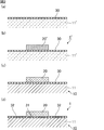
- 2 (a), 2 (b), 2 (c) and 2 (d) are cross-sectional views schematically showing an example of a method for manufacturing the ceramic substrate 1 shown in FIG.
- FIG. 3 is a cross-sectional view schematically showing an example of an electronic component built-in module according to the first embodiment of the present invention.
- FIG. 4 is a cross-sectional view schematically showing an example of a ceramic substrate according to the second embodiment of the present invention.
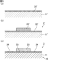
- FIG. 5A, FIG. 5B, and FIG. 5C are cross-sectional views schematically showing an example of a method for manufacturing the ceramic substrate 2 shown in FIG. FIG.
- FIG. 6 is a cross-sectional view schematically showing an example of an electronic component built-in module according to the second embodiment of the present invention.
- FIG. 7 is a cross-sectional view schematically showing an example of a ceramic substrate according to the third embodiment of the present invention.
- FIG. 8A, FIG. 8B, and FIG. 8C are cross-sectional views schematically showing an example of a method for manufacturing the ceramic substrate 3 shown in FIG.
- FIG. 9 is a cross-sectional view schematically showing an example of an electronic component built-in module according to the third embodiment of the present invention.
- a ceramic substrate according to a first embodiment of the present invention includes a ceramic body having a ceramic layer on a surface thereof, and a surface electrode provided on one main surface of the ceramic body, the surface electrode, the ceramic layer, Between these, an oxide layer made of an insulating oxide having a melting point higher than the firing temperature of the ceramic layer is provided.
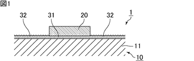
- FIG. 1 is a cross-sectional view schematically showing an example of a ceramic substrate according to the first embodiment of the present invention.
- the ceramic substrate 1 includes a ceramic element body 10 having a ceramic layer 11 on the surface, and a surface electrode 20 provided on one main surface of the ceramic element body 10. I have.
- an oxide layer 31 is provided between the surface electrode 20 and the ceramic layer 11, and the oxide layer 32 is also formed on the ceramic layer 11 where the surface electrode 20 is not provided. Is provided.
- the surface of the oxide layer 32 on the ceramic layer 11 on which the surface electrode 20 is not provided is a rough surface, and the surface roughness of the oxide layer 32 is the oxide layer 31 between the surface electrode 20 and the ceramic layer 11. It is larger than the surface roughness.
- the ceramic body 10 has a laminated structure in which a plurality of ceramic layers 11 are laminated, and an inner layer conductor and a via conductor are provided inside the ceramic body 10. ing.
- a surface electrode may be provided on the other main surface of the ceramic body 10.
- the low-temperature sintered ceramic material contained in the ceramic layer examples include a glass composite low-temperature sintered ceramic material obtained by mixing borosilicate glass with a ceramic material such as quartz, alumina, and forsterite, ZnO—MgO—Al 2 Crystallized glass-based low-temperature sintered ceramic materials using O 3 —SiO 2 -based crystallized glass, BaO—Al 2 O 3 —SiO 2 based ceramic materials and Al 2 O 3 —CaO—SiO 2 —MgO—B 2 Non-glass type low-temperature sintered ceramic material using O 3 type ceramic material or the like can be used.
- the low-temperature sintered ceramic material preferably contains an oxide constituting the oxide layer, and more preferably contains alumina.
- a surface electrode may contain components other than an electroconductive component, it is preferable not to contain a glass component substantially from a viewpoint of preventing the coating
- the oxide layer provided between the surface electrode and the ceramic layer and on the ceramic layer where the surface electrode is not provided is made of an insulating oxide having a melting point higher than the firing temperature of the ceramic layer. .
- the melting point of the oxide constituting the oxide layer is preferably higher than 1000 ° C, more preferably higher than 1800 ° C, and further preferably higher than 2000 ° C.
- the melting point of the oxide constituting the oxide layer is preferably 3000 ° C. or lower.
- Specific examples of the oxide layer include an alumina layer, a titania layer, a zirconia layer, a silica layer, and a magnesia layer. Among these, an alumina layer is preferable.
- the surface roughness of the oxide layer on the ceramic layer not provided with the surface electrode is larger than the surface roughness of the oxide layer between the surface electrode and the ceramic layer
- the surface roughness of the oxide layer on the ceramic layer not provided with the surface electrode is not particularly limited, but is preferably 1 ⁇ m or more and 10 ⁇ m or less. Adhesiveness with resin can be further acquired as it is this range.
- the thickness of the oxide layer is not particularly limited, but is preferably 1 ⁇ m or more and 10 ⁇ m or less. Within this range, wetting of the glass can be effectively prevented. Note that the thickness of the oxide layer is obtained by measuring a cross-polished surface using a microscope.
- the ceramic substrate 1 shown in FIG. 1 is preferably manufactured as follows. 2 (a), 2 (b), 2 (c) and 2 (d) are cross-sectional views schematically showing an example of a method for manufacturing the ceramic substrate 1 shown in FIG.
- the ceramic green sheet becomes a ceramic layer after firing.
- the ceramic green sheet is obtained by forming a slurry containing a ceramic raw material powder such as a low-temperature sintered ceramic material, an organic binder, and a solvent into a sheet shape by a doctor blade method or the like.
- the slurry may contain various additives such as a dispersant and a plasticizer.
- a through hole for a via conductor is formed in a specific ceramic green sheet.
- the through-hole is filled with a conductive paste containing, for example, Ag or Cu as a conductive component, thereby forming a conductive paste body to be a via conductor.
- a conductive paste layer to be an inner layer conductor is formed on a specific ceramic green sheet by a method such as screen printing.
- an oxide layer 30 having a smooth surface is formed on the ceramic green sheet 11 ′ disposed on the surface after lamination.
- the oxide layer 30 is formed on the entire surface of the ceramic green sheet 11 ′.
- the oxide layer 30 can be formed by a method such as screen printing using a paste containing an oxide such as alumina.
- the oxide layer 30 may be formed after the ceramic green sheets 11 ′ are stacked.
- the intervals between the oxide particles constituting the oxide layer are close.
- the particle diameter of oxide particles such as alumina particles is preferably 0.1 ⁇ m or more and 1 ⁇ m or less.
- the thickness of the oxide layer formed on a ceramic green sheet is not specifically limited, It is preferable that they are 1 micrometer or more and 10 micrometers or less. Within this range, wetting of the glass can be effectively prevented.
- a roughening treatment is performed on the surface of the fired laminate. Accordingly, as shown in FIG. 2D, the surface of the oxide layer 32 on the ceramic layer 11 on which the surface electrode 20 is not provided is roughened to become a rough surface, and the ceramic on which the surface electrode 20 is not provided.
- the surface roughness of the oxide layer 32 on the layer 11 is larger than the surface roughness of the oxide layer 31 between the surface electrode 20 and the ceramic layer 11. As a result, it is possible to improve the adhesion with the sealing resin used when the electronic component built-in module is manufactured.
- Examples of the roughening method include a polishing process and a process of spraying an abrasive. If the surface electrode is not adversely affected, the surface of the surface electrode may be roughened, and may be masked as necessary.
- the surface roughness of the oxide layer on the ceramic layer in which the surface electrode is not provided can be about 5 micrometers.
- a plated layer may be formed on the upper surface of the surface electrode by performing electrolytic plating or electroless plating on the fired laminate.
- the ceramic substrate 1 shown in FIG. 1 is obtained.
- a constraining green sheet containing an oxide that does not substantially sinter at the temperature at which the ceramic green sheet sinters is prepared, and laminated in a state where the constraining green sheets are arranged on both main surfaces of the unfired laminate.
- the body may be fired.
- the constraining green sheet does not sinter substantially at the time of firing, so that it does not shrink, and acts to suppress shrinkage in the main surface direction with respect to the laminate. As a result, the dimensional accuracy of the ceramic substrate can be increased.
- the constraining green sheet is preferably formed from a slurry containing the above oxide powder, an organic binder, and a solvent into a sheet shape by a doctor blade method or the like.
- the slurry may contain various additives such as a dispersant and a plasticizer.
- oxide contained in the slurry for example, alumina, titania, zirconia, silica, magnesia and the like can be used. In these, it is preferable to use the same oxide as the oxide which comprises an oxide layer, and it is more preferable to use an alumina.
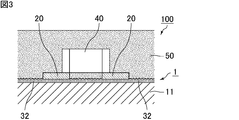
- FIG. 3 is a cross-sectional view schematically showing an example of an electronic component built-in module according to the first embodiment of the present invention.
- the electronic component built-in module 100 shown in FIG. 3 is provided on the main surface of the ceramic substrate 1, the electronic component 40 mounted on the surface electrode 20 of the ceramic substrate 1, and so as to cover the electronic component 40. Sealing resin 50.
- the ceramic substrate 1 shown in FIG. 3 has the same configuration as the ceramic substrate 1 shown in FIG. 1 except that two surface electrodes 20 are provided.
- the sealing resin 50 is excellent in adhesiveness with the sealing resin 50, and even when a force in the lateral direction (the main surface direction of the ceramic substrate 1) is applied to the electronic component built-in module 100, the sealing resin 50 is the ceramic substrate. It becomes difficult to peel from 1.
- the surface electrode and the electronic component are connected by soldering or the like.
- the electronic component is made of, for example, an active component, a passive component, or a composite thereof.
- the active component include semiconductor elements such as transistors, diodes, ICs, and LSIs.
- the passive component include chip-like components such as resistors, capacitors, and inductors, vibrators, filters, and the like.
- the material of the sealing resin is arbitrary, but for example, a curable resin such as an epoxy resin or a polyimide resin can be used.
- the sealing resin is preferably solidified or cured after being placed on the electronic component in a semi-molten state.
- the sealing resin exists between the ceramic substrate and the electronic component, but the sealing resin may exist between the ceramic substrate and the electronic component, A space may be formed without being present.
- the ceramic substrate according to the second embodiment of the present invention includes a ceramic body having a ceramic layer on the surface, and a surface electrode provided on one main surface of the ceramic body.
- An oxide layer made of an insulating oxide having a melting point higher than the firing temperature of the ceramic layer is provided between the surface electrode and the ceramic layer.
- an insulating oxide having a melting point higher than the firing temperature of the ceramic layer is also provided between the surface electrode and the ceramic layer and on the ceramic layer not provided with the surface electrode.
- An oxide layer is provided. The surface of the oxide layer on the ceramic layer on which the surface electrode is not provided is rough, and the surface of the oxide layer between the surface electrode and the ceramic layer is also rough.
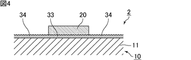
- FIG. 4 is a cross-sectional view schematically showing an example of a ceramic substrate according to the second embodiment of the present invention.
- the ceramic substrate 2 includes a ceramic body 10 having a ceramic layer 11 on the surface and a surface electrode 20 provided on one main surface of the ceramic body 10. I have.
- the oxide layer 33 is provided between the surface electrode 20 and the ceramic layer 11, and the oxide layer 34 is also formed on the ceramic layer 11 where the surface electrode 20 is not provided. Is provided.
- the surface of the oxide layer 34 on the ceramic layer 11 on which the surface electrode 20 is not provided is a rough surface, and the surface of the oxide layer 33 between the surface electrode 20 and the ceramic layer 11 is also a rough surface.
- the configurations of the ceramic body and the surface electrode are the same as in the first embodiment.
- the oxide layer provided between the surface electrode and the ceramic layer and on the ceramic layer where the surface electrode is not provided is made of an insulating oxide having a melting point higher than the firing temperature of the ceramic layer. .
- the melting point of the oxide constituting the oxide layer is preferably higher than 1000 ° C, more preferably higher than 1800 ° C, and further preferably higher than 2000 ° C.
- the melting point of the oxide constituting the oxide layer is preferably 3000 ° C. or lower.
- Specific examples of the oxide layer include an alumina layer, a titania layer, a zirconia layer, a silica layer, and a magnesia layer. Among these, an alumina layer is preferable.
- the surface of the oxide layer on the ceramic layer not provided with the surface electrode, and the surface of the oxide layer between the surface electrode and the ceramic layer may be rough
- the surface roughness of each oxide layer is not particularly limited, but in any case, it is preferably 1 ⁇ m or more and 10 ⁇ m or less. Adhesiveness with resin can be further acquired as it is this range. Note that the surface roughness of the oxide layer on the ceramic layer on which the surface electrode is not provided may be the same as or different from the surface roughness of the oxide layer between the surface electrode and the ceramic layer. Good.
- the thickness of the oxide layer is not particularly limited, but is preferably 1 ⁇ m or more and 10 ⁇ m or less. Within this range, wetting of the glass can be effectively prevented.
- FIG. 5A, FIG. 5B, and FIG. 5C are cross-sectional views schematically showing an example of a method for manufacturing the ceramic substrate 2 shown in FIG.
- a conductive paste body to be a via conductor or a conductive paste layer to be an inner layer conductor is formed on a specific ceramic green sheet.
- an oxide layer 30 ' having a rough surface is formed on the ceramic green sheet 11' disposed on the surface after lamination.
- an oxide layer 30 ′ is formed on the entire surface of the ceramic green sheet 11 ′.
- the oxide layer 30 ' can be formed by a method such as screen printing using a paste containing an oxide such as alumina.
- the oxide layer 30 ′ may be formed after the ceramic green sheets 11 ′ are stacked.
- the intervals between the oxide particles constituting the oxide layer are close.
- oxide particles larger than the thickness of the oxide layer to be formed to the paste by adding oxide particles larger than the thickness of the oxide layer to be formed to the paste, a convex shape is formed on the surface of the oxide layer after firing, and an oxide layer having a rough surface is formed. be able to.
- oxide particles (large particles) having a particle diameter of 5 ⁇ m or more and 10 ⁇ m or less are added to oxide particles (small particles) having a particle diameter of 0.1 ⁇ m or more and 1 ⁇ m or less. It is preferable to add it. What is necessary is just to adjust the size of a large particle, the size of a small particle, the ratio of a large particle and a small particle, etc. according to the adhesiveness with sealing resin calculated
- the thickness of the oxide layer formed on a ceramic green sheet is not specifically limited, It is preferable that they are 1 micrometer or more and 10 micrometers or less. Within this range, wetting of the glass can be effectively prevented.
- the unfired laminate 2 ′ is fired.
- the ceramic body 10 having the ceramic layer 11 on the surface, the oxide layers 33 and 34 provided on the entire main surface of the ceramic body 10, and the oxide A laminate including the surface electrode 20 provided on the layer 33 is obtained.
- the oxide layers 33 and 34 shown in FIG. 5C are the same as the oxide layer 30 ′ shown in FIGS. 5A and 5B.
- the surface of the oxide layer 34 on the ceramic layer 11 on which the surface electrode 20 is not provided is rough. It is a surface. Since the oxide layers 33 and 34 on the surface of the ceramic layer 11 suppress the coating of the glass component on the surface electrode 20, the conductivity of the surface electrode 20 can be ensured. Furthermore, since the surface of the oxide layer 34 on the ceramic layer 11 on which the surface electrode 20 is not provided is a rough surface, the adhesion with the sealing resin used when manufacturing the electronic component built-in module is improved. Can be made.
- a plated layer may be formed on the upper surface of the surface electrode by performing electrolytic plating or electroless plating on the fired laminate.
- the surface of the oxide layer 34 on the ceramic layer 11 on which the surface electrode 20 is not provided is a rough surface. Therefore, the sealing resin 50 is excellent in adhesion with the sealing resin 50, and even when a force in the lateral direction (the main surface direction of the ceramic substrate 2) is applied to the electronic component built-in module 200, the sealing resin 50 is the ceramic substrate. 2 becomes difficult to peel off.
- the ceramic substrate according to the third embodiment of the present invention includes a ceramic body having a ceramic layer on the surface, and a surface electrode provided on one main surface of the ceramic body.
- An oxide layer made of an insulating oxide having a melting point higher than the firing temperature of the ceramic layer is provided between the surface electrode and the ceramic layer.
- FIG. 7 is a cross-sectional view schematically showing an example of a ceramic substrate according to the third embodiment of the present invention.
- the ceramic substrate 3 includes a ceramic body 10 having a ceramic layer 11 on the surface and a surface electrode 20 provided on one main surface of the ceramic body 10. I have.
- the oxide layer 35 is provided between the surface electrode 20 and the ceramic layer 11, and the surface of the ceramic layer 11 in which the surface electrode 20 is not provided is exposed.
- the configurations of the ceramic body and the surface electrode are the same as in the first embodiment.
- the melting point of the oxide constituting the oxide layer is preferably higher than 1000 ° C, more preferably higher than 1800 ° C, and further preferably higher than 2000 ° C.
- the melting point of the oxide constituting the oxide layer is preferably 3000 ° C. or lower.
- Specific examples of the oxide layer include an alumina layer, a titania layer, a zirconia layer, a silica layer, and a magnesia layer. Among these, an alumina layer is preferable.
- the thickness of the oxide layer is not particularly limited, but is preferably 1 ⁇ m or more and 10 ⁇ m or less. Within this range, wetting of the glass can be effectively prevented.
- the size of the oxide layer is not particularly limited as long as the oxide layer is provided between the surface electrode and the ceramic layer.
- FIG. 8A, FIG. 8B, and FIG. 8C are cross-sectional views schematically showing an example of a method for manufacturing the ceramic substrate 3 shown in FIG.
- an oxide layer 35 having a smooth surface is formed on a part of the ceramic green sheet 11 ′ disposed on the surface after lamination.
- the oxide layer 35 can be formed by a method such as screen printing using a paste containing an oxide such as alumina.
- the oxide layer 35 may be formed after the ceramic green sheets 11 ′ are stacked.
- the intervals between the oxide particles constituting the oxide layer are close.
- the particle diameter of oxide particles such as alumina particles is preferably 0.1 ⁇ m or more and 1 ⁇ m or less.
- the thickness of the oxide layer formed on a ceramic green sheet is not specifically limited, It is preferable that they are 1 micrometer or more and 10 micrometers or less. Within this range, wetting of the glass can be effectively prevented.
- a conductive paste layer 20 ′ to be the surface electrode 20 is formed on the oxide layer 35 as in the first embodiment. At this time, it is possible to print by overlapping the oxide layer 35 using a screen plate for forming the oxide layer 35. Subsequently, a plurality of ceramic green sheets 11 ′ are stacked and pressure-bonded to produce an unfired stacked body 3 ′.
- the unfired laminate 3 ′ is fired.
- the ceramic body 10 having the ceramic layer 11 on the surface, the oxide layer 35 provided on a part of one main surface of the ceramic body 10, and the oxide layer A laminate including the surface electrode 20 provided on the surface 35 is obtained.
- the oxide layer 35 is formed between the surface electrode 20 and the ceramic layer 11, and the surface of the ceramic layer 11 where the surface electrode 20 is not provided is exposed. Since the oxide layer 35 on the surface of the ceramic layer 11 suppresses the coating of the glass component on the surface electrode 20, the conductivity of the surface electrode 20 can be ensured. Furthermore, since the surface of the ceramic layer 11 on which the surface electrode 20 is not provided is exposed, it is possible to improve the adhesion with the sealing resin used when producing the electronic component built-in module.
- a plated layer may be formed on the upper surface of the surface electrode by performing electrolytic plating or electroless plating on the fired laminate.
- a constraining green sheet containing an oxide that does not substantially sinter at the temperature at which the ceramic green sheet sinters is prepared, and laminated in a state where the constraining green sheets are arranged on both main surfaces of the unfired laminate.
- the body may be fired.
- FIG. 9 is a cross-sectional view schematically showing an example of an electronic component built-in module according to the third embodiment of the present invention.
- An electronic component built-in module 300 shown in FIG. 9 is provided on the main surface of the ceramic substrate 3, the electronic component 40 mounted on the surface electrode 20 of the ceramic substrate 3, and so as to cover the electronic component 40. Sealing resin 50.
- the ceramic substrate 3 shown in FIG. 9 has the same configuration as the ceramic substrate 3 shown in FIG. 7 except that it includes two surface electrodes 20.
- the sealing resin 50 is excellent in adhesiveness with the sealing resin 50, and even when a force in the lateral direction (the main surface direction of the ceramic substrate 3) is applied to the electronic component built-in module 300, the sealing resin 50 is the ceramic substrate. 3 is difficult to peel off.
- the ceramic substrate and the electronic component built-in module according to the present invention are not limited to the above-described embodiments, but relate to the structure of the ceramic body and the surface electrode, the formation method of the oxide layer, and the like, and various applications within the scope of the invention. It is possible to add deformation.
Landscapes
- Engineering & Computer Science (AREA)
- Microelectronics & Electronic Packaging (AREA)
- Manufacturing & Machinery (AREA)
- Chemical & Material Sciences (AREA)
- Inorganic Chemistry (AREA)
- Ceramic Engineering (AREA)
- Non-Metallic Protective Coatings For Printed Circuits (AREA)
- Physics & Mathematics (AREA)
- Condensed Matter Physics & Semiconductors (AREA)
- General Physics & Mathematics (AREA)
- Production Of Multi-Layered Print Wiring Board (AREA)
- Structures For Mounting Electric Components On Printed Circuit Boards (AREA)
- Manufacturing Of Printed Wiring (AREA)
Abstract
本発明のセラミック基板は、表面にセラミック層を有するセラミック素体と、上記セラミック素体の一方主面に設けられた表面電極とを備えるセラミック基板であって、上記表面電極と上記セラミック層との間に、上記セラミック層の焼成温度よりも高い融点を有する絶縁性の酸化物からなる酸化物層が設けられているとともに、上記表面電極が設けられていない上記セラミック層上にも上記酸化物層が設けられており、上記表面電極が設けられていない上記セラミック層上の上記酸化物層の表面が粗面であることを特徴とする。
Description
本発明は、セラミック基板及び電子部品内蔵モジュールに関する。
セラミック基板上に複数の電子部品が実装され、それらの電子部品が封止樹脂で覆われた電子部品内蔵モジュールが、高機能モジュールとして電子機器等に使用されている(例えば、特許文献1参照)。
特許文献1に記載されているような電子部品内蔵モジュールにおいては、該モジュールを構成するセラミック基板を作製する際の焼成中に、セラミック層から溶解したガラス成分が基板の表面電極上を被覆し、セラミック基板の機能が損なわれるという問題があった。
表面電極上へのガラス成分の被覆を抑制するための手法として、例えば、アルミナ層をセラミック基板の表面に配置した状態でセラミック基板を焼成する方法が提案されている。
上述のように、アルミナ層をセラミック基板の表面に配置した状態でセラミック基板を焼成することにより、表面電極上へのガラス成分の被覆を抑制することができる。しかし、本発明者らが上記セラミック基板を用いて電子部品内蔵モジュールを作製したところ、セラミック基板と封止樹脂との間の密着性が低いという問題が生じることが判明した。
本発明は上記の問題を解決するためになされたものであり、表面電極上へのガラス成分の被覆が抑制されるとともに、電子部品内蔵モジュールにおける封止樹脂との密着性が高いセラミック基板を提供することを目的とする。本発明はまた、該セラミック基板を備える電子部品内蔵モジュールを提供することを目的とする。
本発明のセラミック基板は、表面にセラミック層を有するセラミック素体と、上記セラミック素体の一方主面に設けられた表面電極とを備えるセラミック基板であって、上記表面電極と上記セラミック層との間に、上記セラミック層の焼成温度よりも高い融点を有する絶縁性の酸化物からなる酸化物層が設けられているとともに、上記表面電極が設けられていない上記セラミック層上にも上記酸化物層が設けられており、上記表面電極が設けられていない上記セラミック層上の上記酸化物層の表面が粗面であることを特徴とする。
上記セラミック基板では、表面電極とセラミック層との間に、絶縁性の酸化物からなる酸化物層が設けられている。酸化物層を構成する酸化物は、セラミック層の焼成温度よりも高い融点を有しているため、セラミック層の焼成中に融解することがない。したがって、焼成中にセラミック層から溶解したガラス成分を酸化物層の粒子間に留めることができるため、表面電極上へのガラス成分の被覆(以下、ガラスの濡れ上がりともいう)を抑制することができる。
一方、表面電極が設けられていないセラミック層上にも酸化物層が設けられているが、表面電極が設けられていないセラミック層上の酸化物層の表面は平滑でなく、粗い面となっている。したがって、電子部品内蔵モジュールを作製する際に用いられる封止樹脂との密着性に優れている。
一方、表面電極が設けられていないセラミック層上にも酸化物層が設けられているが、表面電極が設けられていないセラミック層上の酸化物層の表面は平滑でなく、粗い面となっている。したがって、電子部品内蔵モジュールを作製する際に用いられる封止樹脂との密着性に優れている。
一実施形態において、上記表面電極が設けられていない上記セラミック層上の上記酸化物層の表面粗さは、上記表面電極と上記セラミック層との間の上記酸化物層の表面粗さよりも大きい。このような構成によって、封止樹脂との密着性に優れる電子部品内蔵モジュールを提供することが可能である。
上記セラミック基板は、例えば、セラミック層の表面全体に酸化物層を形成し、一部の酸化物層上に表面電極を形成した後、表面電極が形成されていないセラミック層上の酸化物の表面に粗化処理を施すことにより作製することができる。
上記セラミック基板は、例えば、セラミック層の表面全体に酸化物層を形成し、一部の酸化物層上に表面電極を形成した後、表面電極が形成されていないセラミック層上の酸化物の表面に粗化処理を施すことにより作製することができる。
一実施形態において、上記表面電極と上記セラミック層との間の上記酸化物層の表面も粗面である。このような構成によって、封止樹脂との密着性に優れる電子部品内蔵モジュールを提供することが可能である。
上記セラミック基板は、例えば、粒子径の大きな酸化物粒子を含む酸化物層をセラミック層の表面全体に形成した後、一部の酸化物層上に表面電極を形成することにより作製することができる。
上記セラミック基板は、例えば、粒子径の大きな酸化物粒子を含む酸化物層をセラミック層の表面全体に形成した後、一部の酸化物層上に表面電極を形成することにより作製することができる。
本発明のセラミック基板は、表面にセラミック層を有するセラミック素体と、上記セラミック素体の一方主面に設けられた表面電極とを備えるセラミック基板であって、上記表面電極と上記セラミック層との間に、上記セラミック層の焼成温度よりも高い融点を有する絶縁性の酸化物からなる酸化物層が設けられており、上記表面電極が設けられていない上記セラミック層の表面が露出していることを特徴とする。
上記セラミック基板では、表面電極とセラミック層との間に絶縁性の酸化物からなる酸化物層が設けられている。したがって、表面電極上へのガラス成分の被覆を抑制することができる。
一方、表面電極が設けられていないセラミック層上には酸化物層がなく、セラミック層の表面が露出している。したがって、電子部品内蔵モジュールを作製する際に用いられる封止樹脂との密着性に優れている。
一方、表面電極が設けられていないセラミック層上には酸化物層がなく、セラミック層の表面が露出している。したがって、電子部品内蔵モジュールを作製する際に用いられる封止樹脂との密着性に優れている。
本発明のセラミック基板において、上記酸化物層は、アルミナ層であることが好ましい。
通常、セラミック層にアルミナが含まれていることが多く、そのような場合には、焼成中にアルミナ層とセラミック層とが反応したとしても、セラミック層の内部で生成するような化合物が生成するだけであるため、異質な化合物が生成することがない。したがって、セラミック基板の品質が低下しにくくなる。
通常、セラミック層にアルミナが含まれていることが多く、そのような場合には、焼成中にアルミナ層とセラミック層とが反応したとしても、セラミック層の内部で生成するような化合物が生成するだけであるため、異質な化合物が生成することがない。したがって、セラミック基板の品質が低下しにくくなる。
本発明の電子部品内蔵モジュールは、本発明のセラミック基板と、上記セラミック基板の表面電極に実装された電子部品と、上記セラミック基板の主面上に、上記電子部品を覆うように設けられた封止樹脂とを備えることを特徴とする。
上記のとおり、本発明のセラミック基板は封止樹脂との密着性に優れるため、電子部品内蔵モジュールに対して横方向(セラミック基板の主面方向)の力が加わった場合であっても、封止樹脂がセラミック基板から剥がれにくくなる。
本発明によれば、表面電極上へのガラス成分の被覆が抑制されるとともに、電子部品内蔵モジュールにおける封止樹脂との密着性が高いセラミック基板を提供することができる。
以下、本発明のセラミック基板及び電子部品内蔵モジュールの実施形態について説明する。
しかしながら、本発明は、以下の構成に限定されるものではなく、本発明の要旨を変更しない範囲において適宜変更して適用することができる。
なお、以下において記載する個々の実施形態の望ましい構成を2つ以上組み合わせたものもまた本発明である。
しかしながら、本発明は、以下の構成に限定されるものではなく、本発明の要旨を変更しない範囲において適宜変更して適用することができる。
なお、以下において記載する個々の実施形態の望ましい構成を2つ以上組み合わせたものもまた本発明である。
以下に示す各実施形態は例示であり、異なる実施形態で示した構成の部分的な置換又は組み合わせが可能であることは言うまでもない。第2実施形態以降では、第1実施形態と共通の事項についての記述は省略し、異なる点についてのみ説明する。特に、同様の構成による同様の作用効果については、実施形態毎には逐次言及しない。
[第1実施形態]
(セラミック基板)
本発明の第1実施形態に係るセラミック基板は、表面にセラミック層を有するセラミック素体と、上記セラミック素体の一方主面に設けられた表面電極とを備えており、表面電極とセラミック層との間に、セラミック層の焼成温度よりも高い融点を有する絶縁性の酸化物からなる酸化物層が設けられている。
(セラミック基板)
本発明の第1実施形態に係るセラミック基板は、表面にセラミック層を有するセラミック素体と、上記セラミック素体の一方主面に設けられた表面電極とを備えており、表面電極とセラミック層との間に、セラミック層の焼成温度よりも高い融点を有する絶縁性の酸化物からなる酸化物層が設けられている。
本発明の第1実施形態では、表面電極とセラミック層との間に加えて、表面電極が設けられていないセラミック層上にも、セラミック層の焼成温度よりも高い融点を有する絶縁性の酸化物からなる酸化物層が設けられている。表面電極が設けられていないセラミック層上の酸化物層の表面は粗面であり、表面電極が設けられていないセラミック層上の酸化物層の表面粗さは、表面電極とセラミック層との間の酸化物層の表面粗さよりも大きい。
図1は、本発明の第1実施形態に係るセラミック基板の一例を模式的に示す断面図である。
図1には全体的な構成が示されていないが、セラミック基板1は、表面にセラミック層11を有するセラミック素体10と、セラミック素体10の一方主面に設けられた表面電極20とを備えている。
図1には全体的な構成が示されていないが、セラミック基板1は、表面にセラミック層11を有するセラミック素体10と、セラミック素体10の一方主面に設けられた表面電極20とを備えている。
図1に示すセラミック基板1においては、表面電極20とセラミック層11との間に酸化物層31が設けられているとともに、表面電極20が設けられていないセラミック層11上にも酸化物層32が設けられている。表面電極20が設けられていないセラミック層11上の酸化物層32の表面は粗面であり、酸化物層32の表面粗さは、表面電極20とセラミック層11との間の酸化物層31の表面粗さよりも大きくなっている。
図1には示されていないが、セラミック素体10は、複数のセラミック層11が積層された積層構造を有しており、セラミック素体10の内部には、内層導体及びビア導体が設けられている。また、セラミック素体10の他方主面に表面電極が設けられていてもよい。
セラミック素体を構成するセラミック層は、低温焼結セラミック材料を含有することが好ましい。低温焼結セラミック材料とは、セラミック材料のうち、1000℃以下の焼成温度で焼結可能であり、AgやCu等との同時焼成が可能である材料を意味する。
セラミック層に含有される低温焼結セラミック材料としては、例えば、クオーツやアルミナ、フォルステライト等のセラミック材料にホウ珪酸ガラスを混合してなるガラス複合系低温焼結セラミック材料、ZnO-MgO-Al2O3-SiO2系の結晶化ガラスを用いた結晶化ガラス系低温焼結セラミック材料、BaO-Al2O3-SiO2系セラミック材料やAl2O3-CaO-SiO2-MgO-B2O3系セラミック材料等を用いた非ガラス系低温焼結セラミック材料等が挙げられる。酸化物層と反応した場合に異質な化合物が生成することを防止する観点から、低温焼結セラミック材料は、酸化物層を構成する酸化物を含むことが好ましく、アルミナを含むことがより好ましい。
セラミック素体の内部に設けられる内層導体及びビア導体は、導電成分を含有する。内層導体及びビア導体に含有される導電成分としては、例えば、Au、Ag、Cu、Pt、Ta、W、Ni、Fe、Cr、Mo、Ti、Pd、Ru及びこれらの金属の1種を主成分とする合金等が挙げられる。内層導体及びビア導体は、導電成分として、Au、Ag又はCuを含有することが好ましく、Ag又はCuを含有することがより好ましい。Au、Ag及びCuは低抵抗であるため、特に、高周波用途である場合に適している。
セラミック素体の一方主面に設けられた表面電極は、電子部品と接続されるためのものであり、導電成分を含有する。表面電極に含有される導電成分としては、例えば、Au、Ag、Cu、Pt、Ta、W、Ni、Fe、Cr、Mo、Ti、Pd、Ru及びこれらの金属の1種を主成分とする合金等が挙げられる。表面電極は、内層導体及びビア導体と同じ導電成分を含有することが好ましく、具体的には、導電成分として、Au、Ag又はCuを含有することが好ましく、Ag又はCuを含有することがより好ましい。
表面電極は、導電成分以外の成分を含有してもよいが、表面電極上へのガラス成分の被覆を防止する観点から、ガラス成分を実質的に含有しないことが好ましい。
表面電極とセラミック層との間、及び、表面電極が設けられていないセラミック層上に設けられる酸化物層は、いずれも、セラミック層の焼成温度よりも高い融点を有する絶縁性の酸化物からなる。
酸化物層を構成する酸化物の融点は、1000℃より高いことが好ましく、1800℃より高いことがより好ましく、2000℃より高いことがさらに好ましい。また、酸化物層を構成する酸化物の融点は、3000℃以下であることが好ましい。具体的な酸化物層としては、例えば、アルミナ層、チタニア層、ジルコニア層、シリカ層、マグネシア層等が挙げられ、これらの中では、アルミナ層であることが好ましい。
本発明の第1実施形態では、表面電極が設けられていないセラミック層上の酸化物層の表面粗さが、表面電極とセラミック層との間の酸化物層の表面粗さよりも大きければよく、表面電極が設けられていないセラミック層上の酸化物層の表面粗さは特に限定されないが、1μm以上、10μm以下であることが好ましい。この範囲であると、樹脂との密着性をさらに得ることができる。
なお、表面粗さとは、JIS B 0601-2001で規定される最大高さ(Rz)を意味し、表面うねり成分を除去するため、カットオフ値λc=0.250mmとして得るものである。
なお、表面粗さとは、JIS B 0601-2001で規定される最大高さ(Rz)を意味し、表面うねり成分を除去するため、カットオフ値λc=0.250mmとして得るものである。
本発明の第1実施形態において、酸化物層の厚みは特に限定されないが、1μm以上、10μm以下であることが好ましい。この範囲であると、ガラスの濡れ上がりを効果的に防止できる。
なお、酸化物層の厚みは、断面研磨した面を、マイクロスコープを用いて測長して得る。
なお、酸化物層の厚みは、断面研磨した面を、マイクロスコープを用いて測長して得る。
本発明の第1実施形態において、酸化物層は、セラミック層の表面全体に設けられていることが好ましいが、表面電極とセラミック層との間、及び、表面電極が設けられていないセラミック層上に設けられている限り、酸化物層が設けられている範囲は特に限定されない。
図1に示すセラミック基板1は、好ましくは以下のように製造される。
図2(a)、図2(b)、図2(c)及び図2(d)は、図1に示すセラミック基板1の製造方法の一例を模式的に示す断面図である。
図2(a)、図2(b)、図2(c)及び図2(d)は、図1に示すセラミック基板1の製造方法の一例を模式的に示す断面図である。
まず、複数のセラミックグリーンシートを準備する。セラミックグリーンシートは、焼成後にセラミック層となるものである。
セラミックグリーンシートは、例えば低温焼結セラミック材料のようなセラミック原料の粉末と、有機バインダと溶剤とを含有するスラリーを、ドクターブレード法等によってシート状に成形したものである。上記スラリーには、分散剤、可塑剤等の種々の添加剤が含有されていてもよい。
特定のセラミックグリーンシートに、ビア導体のための貫通孔を形成する。該貫通孔に、例えばAg又はCuを導電成分として含有する導電ペーストを充填することにより、ビア導体となるべき導電ペースト体を形成する。
上記導電ペーストと同じ組成の導電ペーストを用いて、例えばスクリーン印刷等の方法によって、特定のセラミックグリーンシートに、内層導体となるべき導電ペースト層を形成する。
次に、図2(a)に示すように、積層後に表面に配置されるセラミックグリーンシート11´上に、表面が平滑な酸化物層30を形成する。図2(a)では、セラミックグリーンシート11´上の全面に酸化物層30を形成している。酸化物層30は、アルミナ等の酸化物を含有するペーストを用いて、例えばスクリーン印刷等の方法によって形成することができる。なお、酸化物層30は、セラミックグリーンシート11´を積層した後に形成してもよい。
表面電極上へのガラス成分の被覆を抑制する観点から、酸化物層を構成する酸化物の粒子の間隔は詰まっていることが好ましい。例えば、アルミナ粒子等の酸化物粒子の粒子径は、0.1μm以上、1μm以下であることが好ましい。
セラミックグリーンシート上に形成する酸化物層の厚みは特に限定されないが、1μm以上、10μm以下であることが好ましい。この範囲であると、ガラスの濡れ上がりを効果的に防止できる。
図2(b)に示すように、一部の酸化物層30上に、表面電極20となるべき導電ペースト層20´を形成する。導電ペースト層20´は、例えば上記導電ペーストと同じ組成の導電ペーストを用いて、スクリーン印刷等の方法によって形成することができる。続いて、複数のセラミックグリーンシート11´を積層し、圧着することにより、未焼成の積層体1´を作製する。
その後、未焼成の積層体1´を焼成する。これによって、図2(c)に示すように、表面にセラミック層11を有するセラミック素体10と、セラミック素体10の一方主面の全面に設けられた酸化物層30と、酸化物層30上に設けられた表面電極20とを備える積層体が得られる。
図2(c)においては、表面電極20とセラミック層11との間だけでなく、表面電極20が設けられていないセラミック層11上にも酸化物層30が形成されており、その表面は平滑である。セラミック層11表面の酸化物層30によって、表面電極20上へのガラス成分の被覆が抑制されるため、表面電極20の導電性を確保することができる。
複合積層体を焼成する際、敷粉を用いてもよい。また、焼成工程の前、又は、焼成工程の後、セラミック積層体を分割する場合もある。
さらに、焼成後の積層体の表面に粗化処理を施す。これによって、図2(d)に示すように、表面電極20が設けられていないセラミック層11上の酸化物層32の表面が粗化されて粗面となり、表面電極20が設けられていないセラミック層11上の酸化物層32の表面粗さが、表面電極20とセラミック層11との間の酸化物層31の表面粗さよりも大きくなる。その結果、電子部品内蔵モジュールを作製する際に用いられる封止樹脂との密着性を向上させることができる。
粗化処理の方法としては、例えば、研磨処理、研磨剤を吹き付ける処理等が挙げられる。表面電極に悪影響を及ぼさなければ、表面電極の表面に粗化処理を施してもよく、また、必要に応じてマスキングをしてもよい。
本発明の第1実施形態では、表面電極が設けられていないセラミック層上の酸化物層の表面粗さを5μm程度にすることができる。
焼成後の積層体に対して、電解めっき又は無電解めっきを施すことによって、表面電極の上面にめっき層を形成してもよい。
以上により、図1に示すセラミック基板1が得られる。
なお、セラミックグリーンシートが焼結する温度では実質的に焼結しない酸化物を含有する拘束用グリーンシートを準備し、未焼成の積層体の両主面に拘束用グリーンシートを配置した状態で積層体を焼成してもよい。
この場合、拘束用グリーンシートは、焼成時において実質的に焼結しないので収縮が生じず、積層体に対して主面方向での収縮を抑制するように作用する。その結果、セラミック基板の寸法精度を高めることができる。
この場合、拘束用グリーンシートは、焼成時において実質的に焼結しないので収縮が生じず、積層体に対して主面方向での収縮を抑制するように作用する。その結果、セラミック基板の寸法精度を高めることができる。
拘束用グリーンシートは、好ましくは、上記酸化物の粉末と有機バインダと溶剤とを含有するスラリーを、ドクターブレード法等によってシート状に成形したものである。上記スラリーには、分散剤、可塑剤等の種々の添加剤が含有されていてもよい。
上記スラリーに含有される酸化物としては、例えば、アルミナ、チタニア、ジルコニア、シリカ、マグネシア等を用いることができる。これらの中では、酸化物層を構成する酸化物と同じ酸化物を用いることが好ましく、アルミナを用いることがより好ましい。
(電子部品内蔵モジュール)
図3は、本発明の第1実施形態に係る電子部品内蔵モジュールの一例を模式的に示す断面図である。
図3に示す電子部品内蔵モジュール100は、セラミック基板1と、セラミック基板1の表面電極20に実装された電子部品40と、セラミック基板1の主面上に、電子部品40を覆うように設けられた封止樹脂50とを備えている。図3に示すセラミック基板1は、表面電極20を2つ備えている点を除いて、図1に示すセラミック基板1と同じ構成を有している。
図3は、本発明の第1実施形態に係る電子部品内蔵モジュールの一例を模式的に示す断面図である。
図3に示す電子部品内蔵モジュール100は、セラミック基板1と、セラミック基板1の表面電極20に実装された電子部品40と、セラミック基板1の主面上に、電子部品40を覆うように設けられた封止樹脂50とを備えている。図3に示すセラミック基板1は、表面電極20を2つ備えている点を除いて、図1に示すセラミック基板1と同じ構成を有している。
上述のように、セラミック基板1では、表面電極20が設けられていないセラミック層11上の酸化物層32の表面が粗面となっている。そのため、封止樹脂50との密着性に優れ、電子部品内蔵モジュール100に対して横方向(セラミック基板1の主面方向)の力が加わった場合であっても、封止樹脂50がセラミック基板1から剥がれにくくなる。
表面電極と電子部品とは、半田付け等によって接続される。電子部品は、例えば、能動部品、受動部品あるいはそれらの複合体からなっている。能動部品としては、例えば、トランジスタ、ダイオード、IC又はLSI等の半導体素子が挙げられ、受動部品としては、例えば、抵抗、コンデンサ又はインダクタ等のチップ状部品や、振動子、フィルタ等が挙げられる。
封止樹脂の材質は任意であるが、例えば、エポキシ樹脂、ポリイミド樹脂等の硬化性樹脂を用いることができる。
封止樹脂は、半溶融状態で電子部品上に配置された後、固化ないし硬化されることが好ましい。図3では、セラミック基板と電子部品との間に封止樹脂が存在しているが、セラミック基板と電子部品との間には、封止樹脂が存在していてもよいし、封止樹脂が存在せずに空間が形成されていてもよい。
[第2実施形態]
(セラミック基板)
本発明の第2実施形態に係るセラミック基板は、本発明の第1実施形態と同様、表面にセラミック層を有するセラミック素体と、上記セラミック素体の一方主面に設けられた表面電極とを備えており、表面電極とセラミック層との間に、セラミック層の焼成温度よりも高い融点を有する絶縁性の酸化物からなる酸化物層が設けられている。
(セラミック基板)
本発明の第2実施形態に係るセラミック基板は、本発明の第1実施形態と同様、表面にセラミック層を有するセラミック素体と、上記セラミック素体の一方主面に設けられた表面電極とを備えており、表面電極とセラミック層との間に、セラミック層の焼成温度よりも高い融点を有する絶縁性の酸化物からなる酸化物層が設けられている。
本発明の第2実施形態では、表面電極とセラミック層との間に加えて、表面電極が設けられていないセラミック層上にも、セラミック層の焼成温度よりも高い融点を有する絶縁性の酸化物からなる酸化物層が設けられている。表面電極が設けられていないセラミック層上の酸化物層の表面は粗面であり、表面電極とセラミック層との間の酸化物層の表面も粗面である。
図4は、本発明の第2実施形態に係るセラミック基板の一例を模式的に示す断面図である。
図4には全体的な構成が示されていないが、セラミック基板2は、表面にセラミック層11を有するセラミック素体10と、セラミック素体10の一方主面に設けられた表面電極20とを備えている。
図4には全体的な構成が示されていないが、セラミック基板2は、表面にセラミック層11を有するセラミック素体10と、セラミック素体10の一方主面に設けられた表面電極20とを備えている。
図4に示すセラミック基板2においては、表面電極20とセラミック層11との間に酸化物層33が設けられているとともに、表面電極20が設けられていないセラミック層11上にも酸化物層34が設けられている。表面電極20が設けられていないセラミック層11上の酸化物層34の表面は粗面であり、表面電極20とセラミック層11との間の酸化物層33の表面も粗面である。
セラミック素体及び表面電極の構成は、第1実施形態と同じである。
表面電極とセラミック層との間、及び、表面電極が設けられていないセラミック層上に設けられる酸化物層は、いずれも、セラミック層の焼成温度よりも高い融点を有する絶縁性の酸化物からなる。
酸化物層を構成する酸化物の融点は、1000℃より高いことが好ましく、1800℃より高いことがより好ましく、2000℃より高いことがさらに好ましい。また、酸化物層を構成する酸化物の融点は、3000℃以下であることが好ましい。具体的な酸化物層としては、例えば、アルミナ層、チタニア層、ジルコニア層、シリカ層、マグネシア層等が挙げられ、これらの中では、アルミナ層であることが好ましい。
本発明の第2実施形態では、表面電極が設けられていないセラミック層上の酸化物層の表面、及び、表面電極とセラミック層との間の酸化物層の表面が粗面であればよく、それぞれの酸化物層の表面粗さは特に限定されないが、いずれも、1μm以上、10μm以下であることが好ましい。この範囲であると、樹脂との密着性をさらに得ることができる。なお、表面電極が設けられていないセラミック層上の酸化物層の表面粗さは、表面電極とセラミック層との間の酸化物層の表面粗さと同じであってもよいし、異なっていてもよい。
本発明の第2実施形態において、酸化物層の厚みは特に限定されないが、1μm以上、10μm以下であることが好ましい。この範囲であると、ガラスの濡れ上がりを効果的に防止できる。
本発明の第2実施形態において、酸化物層は、セラミック層の表面全体に設けられていることが好ましいが、表面電極とセラミック層との間、及び、表面電極が設けられていないセラミック層上に設けられている限り、酸化物層が設けられている範囲は特に限定されない。
図4に示すセラミック基板2は、好ましくは以下のように製造される。
図5(a)、図5(b)及び図5(c)は、図4に示すセラミック基板2の製造方法の一例を模式的に示す断面図である。
図5(a)、図5(b)及び図5(c)は、図4に示すセラミック基板2の製造方法の一例を模式的に示す断面図である。
まず、第1実施形態と同様に、複数のセラミックグリーンシートを準備した後、特定のセラミックグリーンシートに、ビア導体となるべき導電ペースト体又は内層導体となるべき導電ペースト層を形成する。
次に、図5(a)に示すように、積層後に表面に配置されるセラミックグリーンシート11´上に、表面が粗い酸化物層30´を形成する。図5(a)では、セラミックグリーンシート11´上の全面に酸化物層30´を形成している。酸化物層30´は、アルミナ等の酸化物を含有するペーストを用いて、例えばスクリーン印刷等の方法によって形成することができる。なお、酸化物層30´は、セラミックグリーンシート11´を積層した後に形成してもよい。
表面電極上へのガラス成分の被覆を抑制する観点から、酸化物層を構成する酸化物の粒子の間隔は詰まっていることが好ましい。一方、形成する酸化物層の厚みよりも大きな酸化物の粒子をペーストに添加しておくことにより、焼成後の酸化物層の表面に凸形状を形成し、表面が粗い酸化物層を形成することができる。例えば、厚み3μm程度の酸化物層を形成する場合、粒子径が0.1μm以上、1μm以下の酸化物粒子(小型粒子)に粒子径が5μm以上、10μm以下の酸化物粒子(大型粒子)を添加しておくことが好ましい。大型粒子のサイズ、小型粒子のサイズ、大型粒子と小型粒子の比率等は、求められる封止樹脂との密着性に応じて調整すればよい。
本発明の第2実施形態では、酸化物層の表面粗さを2μm程度にすることができる。
セラミックグリーンシート上に形成する酸化物層の厚みは特に限定されないが、1μm以上、10μm以下であることが好ましい。この範囲であると、ガラスの濡れ上がりを効果的に防止できる。
図5(b)に示すように、一部の酸化物層30´上に、第1実施形態と同様に、表面電極20となるべき導電ペースト層20´を形成する。続いて、複数のセラミックグリーンシート11´を積層し、圧着することにより、未焼成の積層体2´を作製する。
その後、未焼成の積層体2´を焼成する。これによって、図5(c)に示すように、表面にセラミック層11を有するセラミック素体10と、セラミック素体10の一方主面の全面に設けられた酸化物層33及び34と、酸化物層33上に設けられた表面電極20とを備える積層体が得られる。なお、図5(c)に示す酸化物層33及び34は、図5(a)及び図5(b)に示す酸化物層30´と同じである。
図5(c)においては、表面電極20が設けられていないセラミック層11上の酸化物層34の表面だけでなく、表面電極20とセラミック層11との間の酸化物層33の表面も粗面となっている。セラミック層11表面の酸化物層33及び34によって、表面電極20上へのガラス成分の被覆が抑制されるため、表面電極20の導電性を確保することができる。さらに、表面電極20が設けられていないセラミック層11上の酸化物層34の表面が粗面となっているため、電子部品内蔵モジュールを作製する際に用いられる封止樹脂との密着性を向上させることができる。
焼成後の積層体に対して、電解めっき又は無電解めっきを施すことによって、表面電極の上面にめっき層を形成してもよい。
以上により、図4に示すセラミック基板2が得られる。
なお、セラミックグリーンシートが焼結する温度では実質的に焼結しない酸化物を含有する拘束用グリーンシートを準備し、未焼成の積層体の両主面に拘束用グリーンシートを配置した状態で積層体を焼成してもよい。
(電子部品内蔵モジュール)
図6は、本発明の第2実施形態に係る電子部品内蔵モジュールの一例を模式的に示す断面図である。
図6に示す電子部品内蔵モジュール200は、セラミック基板2と、セラミック基板2の表面電極20に実装された電子部品40と、セラミック基板2の主面上に、電子部品40を覆うように設けられた封止樹脂50とを備えている。図6に示すセラミック基板2は、表面電極20を2つ備えている点を除いて、図4に示すセラミック基板2と同じ構成を有している。
図6は、本発明の第2実施形態に係る電子部品内蔵モジュールの一例を模式的に示す断面図である。
図6に示す電子部品内蔵モジュール200は、セラミック基板2と、セラミック基板2の表面電極20に実装された電子部品40と、セラミック基板2の主面上に、電子部品40を覆うように設けられた封止樹脂50とを備えている。図6に示すセラミック基板2は、表面電極20を2つ備えている点を除いて、図4に示すセラミック基板2と同じ構成を有している。
上述のように、セラミック基板2では、表面電極20が設けられていないセラミック層11上の酸化物層34の表面が粗面となっている。そのため、封止樹脂50との密着性に優れ、電子部品内蔵モジュール200に対して横方向(セラミック基板2の主面方向)の力が加わった場合であっても、封止樹脂50がセラミック基板2から剥がれにくくなる。
[第3実施形態]
(セラミック基板)
本発明の第3実施形態に係るセラミック基板は、本発明の第1実施形態と同様、表面にセラミック層を有するセラミック素体と、上記セラミック素体の一方主面に設けられた表面電極とを備えており、表面電極とセラミック層との間に、セラミック層の焼成温度よりも高い融点を有する絶縁性の酸化物からなる酸化物層が設けられている。
(セラミック基板)
本発明の第3実施形態に係るセラミック基板は、本発明の第1実施形態と同様、表面にセラミック層を有するセラミック素体と、上記セラミック素体の一方主面に設けられた表面電極とを備えており、表面電極とセラミック層との間に、セラミック層の焼成温度よりも高い融点を有する絶縁性の酸化物からなる酸化物層が設けられている。
本発明の第3実施形態では、表面電極が設けられていないセラミック層上には酸化物層がなく、セラミック層の表面が露出している。
図7は、本発明の第3実施形態に係るセラミック基板の一例を模式的に示す断面図である。
図7には全体的な構成が示されていないが、セラミック基板3は、表面にセラミック層11を有するセラミック素体10と、セラミック素体10の一方主面に設けられた表面電極20とを備えている。
図7には全体的な構成が示されていないが、セラミック基板3は、表面にセラミック層11を有するセラミック素体10と、セラミック素体10の一方主面に設けられた表面電極20とを備えている。
図7に示すセラミック基板3においては、表面電極20とセラミック層11との間に酸化物層35が設けられており、表面電極20が設けられていないセラミック層11の表面は露出している。
セラミック素体及び表面電極の構成は、第1実施形態と同じである。
表面電極とセラミック層との間に設けられる酸化物層は、セラミック層の焼成温度よりも高い融点を有する絶縁性の酸化物からなる。
酸化物層を構成する酸化物の融点は、1000℃より高いことが好ましく、1800℃より高いことがより好ましく、2000℃より高いことがさらに好ましい。また、酸化物層を構成する酸化物の融点は、3000℃以下であることが好ましい。具体的な酸化物層としては、例えば、アルミナ層、チタニア層、ジルコニア層、シリカ層、マグネシア層等が挙げられ、これらの中では、アルミナ層であることが好ましい。
本発明の第3実施形態において、酸化物層の厚みは特に限定されないが、1μm以上、10μm以下であることが好ましい。この範囲であると、ガラスの濡れ上がりを効果的に防止できる。
本発明の第3実施形態においては、表面電極とセラミック層との間に酸化物層が設けられている限り、酸化物層のサイズは特に限定されない。
図7に示すセラミック基板3は、好ましくは以下のように製造される。
図8(a)、図8(b)及び図8(c)は、図7に示すセラミック基板3の製造方法の一例を模式的に示す断面図である。
図8(a)、図8(b)及び図8(c)は、図7に示すセラミック基板3の製造方法の一例を模式的に示す断面図である。
まず、第1実施形態と同様に、複数のセラミックグリーンシートを準備した後、特定のセラミックグリーンシートに、ビア導体となるべき導電ペースト体又は内層導体となるべき導電ペースト層を形成する。
次に、図8(a)に示すように、積層後に表面に配置されるセラミックグリーンシート11´上の一部に、表面が平滑な酸化物層35を形成する。酸化物層35は、アルミナ等の酸化物を含有するペーストを用いて、例えばスクリーン印刷等の方法によって形成することができる。なお、酸化物層35は、セラミックグリーンシート11´を積層した後に形成してもよい。
表面電極上へのガラス成分の被覆を抑制する観点から、酸化物層を構成する酸化物の粒子の間隔は詰まっていることが好ましい。例えば、アルミナ粒子等の酸化物粒子の粒子径は、0.1μm以上、1μm以下であることが好ましい。
セラミックグリーンシート上に形成する酸化物層の厚みは特に限定されないが、1μm以上、10μm以下であることが好ましい。この範囲であると、ガラスの濡れ上がりを効果的に防止できる。
図8(b)に示すように、酸化物層35上に、第1実施形態と同様に、表面電極20となるべき導電ペースト層20´を形成する。この際、酸化物層35を形成するためのスクリーン版を用いて、酸化物層35と重ねて印刷することができる。続いて、複数のセラミックグリーンシート11´を積層し、圧着することにより、未焼成の積層体3´を作製する。
その後、未焼成の積層体3´を焼成する。これによって、図8(c)に示すように、表面にセラミック層11を有するセラミック素体10と、セラミック素体10の一方主面の一部に設けられた酸化物層35と、酸化物層35上に設けられた表面電極20とを備える積層体が得られる。
図8(c)においては、表面電極20とセラミック層11との間に酸化物層35が形成されており、表面電極20が設けられていないセラミック層11の表面は露出している。セラミック層11表面の酸化物層35によって、表面電極20上へのガラス成分の被覆が抑制されるため、表面電極20の導電性を確保することができる。さらに、表面電極20が設けられていないセラミック層11の表面は露出しているため、電子部品内蔵モジュールを作製する際に用いられる封止樹脂との密着性を向上させることができる。
焼成後の積層体に対して、電解めっき又は無電解めっきを施すことによって、表面電極の上面にめっき層を形成してもよい。
以上により、図7に示すセラミック基板3が得られる。
なお、セラミックグリーンシートが焼結する温度では実質的に焼結しない酸化物を含有する拘束用グリーンシートを準備し、未焼成の積層体の両主面に拘束用グリーンシートを配置した状態で積層体を焼成してもよい。
(電子部品内蔵モジュール)
図9は、本発明の第3実施形態に係る電子部品内蔵モジュールの一例を模式的に示す断面図である。
図9に示す電子部品内蔵モジュール300は、セラミック基板3と、セラミック基板3の表面電極20に実装された電子部品40と、セラミック基板3の主面上に、電子部品40を覆うように設けられた封止樹脂50とを備えている。図9に示すセラミック基板3は、表面電極20を2つ備えている点を除いて、図7に示すセラミック基板3と同じ構成を有している。
図9は、本発明の第3実施形態に係る電子部品内蔵モジュールの一例を模式的に示す断面図である。
図9に示す電子部品内蔵モジュール300は、セラミック基板3と、セラミック基板3の表面電極20に実装された電子部品40と、セラミック基板3の主面上に、電子部品40を覆うように設けられた封止樹脂50とを備えている。図9に示すセラミック基板3は、表面電極20を2つ備えている点を除いて、図7に示すセラミック基板3と同じ構成を有している。
上述のように、セラミック基板3では、表面電極20が設けられていないセラミック層11の表面が露出している。そのため、封止樹脂50との密着性に優れ、電子部品内蔵モジュール300に対して横方向(セラミック基板3の主面方向)の力が加わった場合であっても、封止樹脂50がセラミック基板3から剥がれにくくなる。
[その他の実施形態]
本発明のセラミック基板及び電子部品内蔵モジュールは、上記実施形態に限定されるものではなく、セラミック素体及び表面電極の構成、酸化物層の形成方法等に関し、発明の範囲内において、種々の応用、変形を加えることが可能である。
本発明のセラミック基板及び電子部品内蔵モジュールは、上記実施形態に限定されるものではなく、セラミック素体及び表面電極の構成、酸化物層の形成方法等に関し、発明の範囲内において、種々の応用、変形を加えることが可能である。
1,2,3 セラミック基板
10 セラミック素体
11 セラミック層
20 表面電極
30,30´,31,32,33,34,35 酸化物層
40 電子部品
50 封止樹脂
100,200,300 電子部品内蔵モジュール
10 セラミック素体
11 セラミック層
20 表面電極
30,30´,31,32,33,34,35 酸化物層
40 電子部品
50 封止樹脂
100,200,300 電子部品内蔵モジュール
Claims (6)
- 表面にセラミック層を有するセラミック素体と、前記セラミック素体の一方主面に設けられた表面電極とを備えるセラミック基板であって、
前記表面電極と前記セラミック層との間に、前記セラミック層の焼成温度よりも高い融点を有する絶縁性の酸化物からなる酸化物層が設けられているとともに、
前記表面電極が設けられていない前記セラミック層上にも前記酸化物層が設けられており、
前記表面電極が設けられていない前記セラミック層上の前記酸化物層の表面が粗面であることを特徴とするセラミック基板。 - 前記表面電極が設けられていない前記セラミック層上の前記酸化物層の表面粗さは、前記表面電極と前記セラミック層との間の前記酸化物層の表面粗さよりも大きい請求項1に記載のセラミック基板。
- 前記表面電極と前記セラミック層との間の前記酸化物層の表面も粗面である請求項1に記載のセラミック基板。
- 表面にセラミック層を有するセラミック素体と、前記セラミック素体の一方主面に設けられた表面電極とを備えるセラミック基板であって、
前記表面電極と前記セラミック層との間に、前記セラミック層の焼成温度よりも高い融点を有する絶縁性の酸化物からなる酸化物層が設けられており、
前記表面電極が設けられていない前記セラミック層の表面が露出していることを特徴とするセラミック基板。 - 前記酸化物層は、アルミナ層である請求項1~4のいずれか1項に記載のセラミック基板。
- 請求項1~5のいずれか1項に記載のセラミック基板と、
前記セラミック基板の表面電極に実装された電子部品と、
前記セラミック基板の主面上に、前記電子部品を覆うように設けられた封止樹脂とを備えることを特徴とする電子部品内蔵モジュール。
Priority Applications (5)
| Application Number | Priority Date | Filing Date | Title |
|---|---|---|---|
| JP2018535553A JP6922918B2 (ja) | 2016-08-22 | 2017-07-31 | セラミック基板及び電子部品内蔵モジュール |
| CN201780049105.8A CN109565939B (zh) | 2016-08-22 | 2017-07-31 | 陶瓷基板和电子部件内置模块 |
| US16/281,269 US11246215B2 (en) | 2016-08-22 | 2019-02-21 | Ceramic substrate and electronic component-embedded module |
| US17/307,300 US11553592B2 (en) | 2016-08-22 | 2021-05-04 | Ceramic substrate and electronic component-embedded module |
| US17/645,323 US20220117084A1 (en) | 2016-08-22 | 2021-12-21 | Ceramic substrate and electronic component-embedded module |
Applications Claiming Priority (2)
| Application Number | Priority Date | Filing Date | Title |
|---|---|---|---|
| JP2016161717 | 2016-08-22 | ||
| JP2016-161717 | 2016-08-22 |
Related Child Applications (1)
| Application Number | Title | Priority Date | Filing Date |
|---|---|---|---|
| US16/281,269 Continuation US11246215B2 (en) | 2016-08-22 | 2019-02-21 | Ceramic substrate and electronic component-embedded module |
Publications (1)
| Publication Number | Publication Date |
|---|---|
| WO2018037842A1 true WO2018037842A1 (ja) | 2018-03-01 |
Family
ID=61246672
Family Applications (1)
| Application Number | Title | Priority Date | Filing Date |
|---|---|---|---|
| PCT/JP2017/027723 Ceased WO2018037842A1 (ja) | 2016-08-22 | 2017-07-31 | セラミック基板及び電子部品内蔵モジュール |
Country Status (4)
| Country | Link |
|---|---|
| US (3) | US11246215B2 (ja) |
| JP (2) | JP6922918B2 (ja) |
| CN (1) | CN109565939B (ja) |
| WO (1) | WO2018037842A1 (ja) |
Cited By (3)
| Publication number | Priority date | Publication date | Assignee | Title |
|---|---|---|---|---|
| WO2021033553A1 (ja) * | 2019-08-16 | 2021-02-25 | デンカ株式会社 | セラミックス基板、回路基板及びその製造方法、並びにパワーモジュール |
| WO2023145784A1 (ja) * | 2022-01-31 | 2023-08-03 | 富士フイルム株式会社 | 配線基板及びその製造方法、フィルム、並びに、積層体 |
| JP7567861B2 (ja) | 2022-05-24 | 2024-10-16 | 株式会社村田製作所 | 電子部品およびその製造方法 |
Families Citing this family (2)
| Publication number | Priority date | Publication date | Assignee | Title |
|---|---|---|---|---|
| CN109565939B (zh) | 2016-08-22 | 2022-04-05 | 株式会社村田制作所 | 陶瓷基板和电子部件内置模块 |
| JP7654164B2 (ja) * | 2022-06-02 | 2025-03-31 | 株式会社東芝 | セラミックス回路基板およびそれを用いた半導体装置 |
Citations (3)
| Publication number | Priority date | Publication date | Assignee | Title |
|---|---|---|---|---|
| JPH10256731A (ja) * | 1997-03-14 | 1998-09-25 | Matsushita Electric Works Ltd | セラミック多層配線板の製造方法 |
| JP2003110238A (ja) * | 2001-09-28 | 2003-04-11 | Murata Mfg Co Ltd | ガラスセラミック多層基板の製造方法 |
| JP2005197354A (ja) * | 2004-01-05 | 2005-07-21 | Renesas Technology Corp | 半導体モジュール及びその製造方法 |
Family Cites Families (22)
| Publication number | Priority date | Publication date | Assignee | Title |
|---|---|---|---|---|
| US2862827A (en) * | 1954-05-20 | 1958-12-02 | Vitro Corp Of America | Ceramic bodies and methods for producing same |
| US3061911A (en) * | 1958-01-31 | 1962-11-06 | Xerox Corp | Method of making printed circuits |
| JPS6184037A (ja) | 1984-09-30 | 1986-04-28 | Toshiba Corp | 窒化アルミニウム系セラミツクス基板 |
| US5242535A (en) * | 1992-09-29 | 1993-09-07 | The Boc Group, Inc. | Method of forming a copper circuit pattern |
| JP3780386B2 (ja) * | 1996-03-28 | 2006-05-31 | 株式会社村田製作所 | セラミック回路基板及びその製造方法 |
| JP3059117B2 (ja) * | 1996-05-31 | 2000-07-04 | 株式会社東芝 | セラミックス回路基板 |
| JPH1083938A (ja) * | 1996-09-09 | 1998-03-31 | Kenwood Corp | 薄膜チップ部品及びその製造方法 |
| JP3173410B2 (ja) * | 1997-03-14 | 2001-06-04 | 松下電器産業株式会社 | パッケージ基板およびその製造方法 |
| JPH11268968A (ja) | 1998-03-20 | 1999-10-05 | Toshiba Corp | セラミックス回路基板 |
| US6228196B1 (en) * | 1998-06-05 | 2001-05-08 | Murata Manufacturing Co., Ltd. | Method of producing a multi-layer ceramic substrate |
| JP2001135933A (ja) * | 1999-11-04 | 2001-05-18 | Murata Mfg Co Ltd | 多層セラミック基板 |
| JP2001244376A (ja) * | 2000-02-28 | 2001-09-07 | Hitachi Ltd | 半導体装置 |
| US6759740B2 (en) | 2001-03-30 | 2004-07-06 | Kyocera Corporation | Composite ceramic board, method of producing the same, optical/electronic-mounted circuit substrate using said board, and mounted board equipped with said circuit substrate |
| JP2005183430A (ja) | 2003-12-16 | 2005-07-07 | Matsushita Electric Ind Co Ltd | 電子部品内蔵モジュール |
| TW200714163A (en) * | 2005-09-16 | 2007-04-01 | Murata Manufacturing Co | Ceramic multilayer substrate and process for producing the same |
| JP2008266065A (ja) * | 2007-04-19 | 2008-11-06 | Murata Mfg Co Ltd | セラミック原料組成物、セラミック焼結体、多層セラミック基板およびその製造方法、ならびに多層セラミック基板作製用複合グリーンシート |
| JP2009059870A (ja) * | 2007-08-31 | 2009-03-19 | Sanyo Electric Co Ltd | 発光モジュールおよびその製造方法 |
| US8609993B2 (en) * | 2008-05-16 | 2013-12-17 | Mitsubishi Materials Corporation | Power module substrate, power module, and method for manufacturing power module substrate |
| JP6058988B2 (ja) * | 2012-11-30 | 2017-01-11 | 京セラ株式会社 | 配線基板の製造方法 |
| JP5983700B2 (ja) * | 2013-12-09 | 2016-09-06 | 株式会社デンソー | 半導体装置およびその製造方法、複合成形体 |
| WO2015178482A1 (ja) * | 2014-05-23 | 2015-11-26 | デクセリアルズ株式会社 | 接着剤及び接続構造体 |
| CN109565939B (zh) | 2016-08-22 | 2022-04-05 | 株式会社村田制作所 | 陶瓷基板和电子部件内置模块 |
-
2017
- 2017-07-31 CN CN201780049105.8A patent/CN109565939B/zh active Active
- 2017-07-31 JP JP2018535553A patent/JP6922918B2/ja active Active
- 2017-07-31 WO PCT/JP2017/027723 patent/WO2018037842A1/ja not_active Ceased
-
2019
- 2019-02-21 US US16/281,269 patent/US11246215B2/en active Active
-
2021
- 2021-05-04 US US17/307,300 patent/US11553592B2/en active Active
- 2021-07-29 JP JP2021124202A patent/JP2021176202A/ja active Pending
- 2021-12-21 US US17/645,323 patent/US20220117084A1/en not_active Abandoned
Patent Citations (3)
| Publication number | Priority date | Publication date | Assignee | Title |
|---|---|---|---|---|
| JPH10256731A (ja) * | 1997-03-14 | 1998-09-25 | Matsushita Electric Works Ltd | セラミック多層配線板の製造方法 |
| JP2003110238A (ja) * | 2001-09-28 | 2003-04-11 | Murata Mfg Co Ltd | ガラスセラミック多層基板の製造方法 |
| JP2005197354A (ja) * | 2004-01-05 | 2005-07-21 | Renesas Technology Corp | 半導体モジュール及びその製造方法 |
Cited By (5)
| Publication number | Priority date | Publication date | Assignee | Title |
|---|---|---|---|---|
| WO2021033553A1 (ja) * | 2019-08-16 | 2021-02-25 | デンカ株式会社 | セラミックス基板、回路基板及びその製造方法、並びにパワーモジュール |
| JP2021031310A (ja) * | 2019-08-16 | 2021-03-01 | デンカ株式会社 | セラミックス基板、回路基板及びその製造方法、並びにパワーモジュール |
| JP7198178B2 (ja) | 2019-08-16 | 2022-12-28 | デンカ株式会社 | セラミックス基板、回路基板及びその製造方法、並びにパワーモジュール |
| WO2023145784A1 (ja) * | 2022-01-31 | 2023-08-03 | 富士フイルム株式会社 | 配線基板及びその製造方法、フィルム、並びに、積層体 |
| JP7567861B2 (ja) | 2022-05-24 | 2024-10-16 | 株式会社村田製作所 | 電子部品およびその製造方法 |
Also Published As
| Publication number | Publication date |
|---|---|
| JP6922918B2 (ja) | 2021-08-18 |
| US20210259105A1 (en) | 2021-08-19 |
| CN109565939A (zh) | 2019-04-02 |
| US11553592B2 (en) | 2023-01-10 |
| US20190191562A1 (en) | 2019-06-20 |
| US11246215B2 (en) | 2022-02-08 |
| CN109565939B (zh) | 2022-04-05 |
| US20220117084A1 (en) | 2022-04-14 |
| JP2021176202A (ja) | 2021-11-04 |
| JPWO2018037842A1 (ja) | 2019-06-20 |
Similar Documents
| Publication | Publication Date | Title |
|---|---|---|
| JP2021176202A (ja) | セラミック基板及び電子部品内蔵モジュール | |
| JP2014123707A (ja) | 基板内蔵用積層セラミック電子部品及びその製造方法、並びに基板内蔵用積層セラミック電子部品を備えるプリント基板 | |
| JP5182367B2 (ja) | 多層セラミック基板およびその製造方法 | |
| JP5024064B2 (ja) | 多層セラミック基板およびその製造方法 | |
| JP6624282B2 (ja) | 多層セラミック基板 | |
| CN109156080B (zh) | 陶瓷电子部件 | |
| JPWO2019059017A1 (ja) | セラミック基板の製造方法、セラミック基板、及び、モジュール | |
| JP4788544B2 (ja) | 多層セラミック基板およびその製造方法 | |
| JP5582069B2 (ja) | セラミック多層基板 | |
| JP2009170848A (ja) | セラミック電子部品及びその製造方法 | |
| JP4038602B2 (ja) | 導電性ペースト及びセラミック多層基板 | |
| JP4673086B2 (ja) | ビア導体メタライズ用の導体ペーストおよびこれを用いたセラミック配線基板の製造方法 | |
| US8241449B2 (en) | Method for producing ceramic body | |
| JP2022083968A (ja) | 積層型電子部品及びその実装基板 | |
| JP4844317B2 (ja) | セラミック電子部品およびその製造方法 | |
| JP2004119547A (ja) | セラミック配線基板およびその製造方法 | |
| JP6962369B2 (ja) | 配線基板 | |
| JP4466863B2 (ja) | 多層セラミックス基板 | |
| JP5563036B2 (ja) | 多層セラミック基板及びその製造方法 | |
| JP5533120B2 (ja) | 多層セラミック基板の製造方法 | |
| JP5209563B2 (ja) | 多層セラミック基板の製造方法 | |
| JP2008186907A (ja) | 多層回路基板の製造方法 | |
| WO2017217174A1 (ja) | セラミック電子部品 | |
| JP2008016572A (ja) | 配線基板およびその製造方法 |
Legal Events
| Date | Code | Title | Description |
|---|---|---|---|
| 121 | Ep: the epo has been informed by wipo that ep was designated in this application |
Ref document number: 17843328 Country of ref document: EP Kind code of ref document: A1 |
|
| ENP | Entry into the national phase |
Ref document number: 2018535553 Country of ref document: JP Kind code of ref document: A |
|
| NENP | Non-entry into the national phase |
Ref country code: DE |
|
| 122 | Ep: pct application non-entry in european phase |
Ref document number: 17843328 Country of ref document: EP Kind code of ref document: A1 |