WO2017018533A1 - Procédé de production de plaquette de monocristal de carbure de silicium épitaxiale - Google Patents
Procédé de production de plaquette de monocristal de carbure de silicium épitaxiale Download PDFInfo
- Publication number
- WO2017018533A1 WO2017018533A1 PCT/JP2016/072421 JP2016072421W WO2017018533A1 WO 2017018533 A1 WO2017018533 A1 WO 2017018533A1 JP 2016072421 W JP2016072421 W JP 2016072421W WO 2017018533 A1 WO2017018533 A1 WO 2017018533A1
- Authority
- WO
- WIPO (PCT)
- Prior art keywords
- single crystal
- silicon carbide
- epitaxial
- crystal substrate
- growth
- Prior art date
Links
- HBMJWWWQQXIZIP-UHFFFAOYSA-N silicon carbide Chemical compound [Si+]#[C-] HBMJWWWQQXIZIP-UHFFFAOYSA-N 0.000 title claims abstract description 214
- 229910010271 silicon carbide Inorganic materials 0.000 title claims abstract description 212
- 239000013078 crystal Substances 0.000 title claims abstract description 184
- 238000004519 manufacturing process Methods 0.000 title claims abstract description 28
- 239000000758 substrate Substances 0.000 claims abstract description 161
- 238000005530 etching Methods 0.000 claims abstract description 119
- 238000000034 method Methods 0.000 claims abstract description 21
- 238000002230 thermal chemical vapour deposition Methods 0.000 claims abstract description 7
- 239000007789 gas Substances 0.000 claims description 50
- UFHFLCQGNIYNRP-UHFFFAOYSA-N Hydrogen Chemical compound [H][H] UFHFLCQGNIYNRP-UHFFFAOYSA-N 0.000 claims description 31
- 239000003575 carbonaceous material Substances 0.000 claims description 14
- 239000002210 silicon-based material Substances 0.000 claims description 14
- 125000004429 atom Chemical group 0.000 claims description 8
- 125000004432 carbon atom Chemical group C* 0.000 claims description 5
- XUIMIQQOPSSXEZ-UHFFFAOYSA-N Silicon Chemical compound [Si] XUIMIQQOPSSXEZ-UHFFFAOYSA-N 0.000 claims 1
- 238000003763 carbonization Methods 0.000 claims 1
- 229910021421 monocrystalline silicon Inorganic materials 0.000 claims 1
- 229910052710 silicon Inorganic materials 0.000 claims 1
- 239000010703 silicon Substances 0.000 claims 1
- 239000010409 thin film Substances 0.000 abstract description 4
- 239000010408 film Substances 0.000 description 79
- 238000006243 chemical reaction Methods 0.000 description 41
- 230000003746 surface roughness Effects 0.000 description 13
- 230000007547 defect Effects 0.000 description 12
- 239000000463 material Substances 0.000 description 10
- 230000000052 comparative effect Effects 0.000 description 9
- 230000015572 biosynthetic process Effects 0.000 description 6
- 230000000694 effects Effects 0.000 description 6
- 230000009467 reduction Effects 0.000 description 6
- 230000008569 process Effects 0.000 description 5
- XKRFYHLGVUSROY-UHFFFAOYSA-N Argon Chemical compound [Ar] XKRFYHLGVUSROY-UHFFFAOYSA-N 0.000 description 2
- 230000002411 adverse Effects 0.000 description 2
- 238000005229 chemical vapour deposition Methods 0.000 description 2
- 230000007423 decrease Effects 0.000 description 2
- 230000003247 decreasing effect Effects 0.000 description 2
- 230000006866 deterioration Effects 0.000 description 2
- 239000001257 hydrogen Substances 0.000 description 2
- 229910052739 hydrogen Inorganic materials 0.000 description 2
- 238000000879 optical micrograph Methods 0.000 description 2
- 238000005498 polishing Methods 0.000 description 2
- 230000001737 promoting effect Effects 0.000 description 2
- 239000004065 semiconductor Substances 0.000 description 2
- OKTJSMMVPCPJKN-UHFFFAOYSA-N Carbon Chemical compound [C] OKTJSMMVPCPJKN-UHFFFAOYSA-N 0.000 description 1
- 208000032544 Cicatrix Diseases 0.000 description 1
- 244000000626 Daucus carota Species 0.000 description 1
- 235000002767 Daucus carota Nutrition 0.000 description 1
- 229910003902 SiCl 4 Inorganic materials 0.000 description 1
- BLRPTPMANUNPDV-UHFFFAOYSA-N Silane Chemical compound [SiH4] BLRPTPMANUNPDV-UHFFFAOYSA-N 0.000 description 1
- 239000003082 abrasive agent Substances 0.000 description 1
- 230000002776 aggregation Effects 0.000 description 1
- 238000004220 aggregation Methods 0.000 description 1
- 238000000137 annealing Methods 0.000 description 1
- 229910052786 argon Inorganic materials 0.000 description 1
- 230000004888 barrier function Effects 0.000 description 1
- 229910052799 carbon Inorganic materials 0.000 description 1
- 239000000919 ceramic Substances 0.000 description 1
- 230000008859 change Effects 0.000 description 1
- SLLGVCUQYRMELA-UHFFFAOYSA-N chlorosilicon Chemical compound Cl[Si] SLLGVCUQYRMELA-UHFFFAOYSA-N 0.000 description 1
- 229910021419 crystalline silicon Inorganic materials 0.000 description 1
- 230000003111 delayed effect Effects 0.000 description 1
- 238000010586 diagram Methods 0.000 description 1
- 229910003460 diamond Inorganic materials 0.000 description 1
- 239000010432 diamond Substances 0.000 description 1
- 239000002019 doping agent Substances 0.000 description 1
- 238000011156 evaluation Methods 0.000 description 1
- 238000001704 evaporation Methods 0.000 description 1
- 230000002349 favourable effect Effects 0.000 description 1
- -1 for example Chemical compound 0.000 description 1
- 235000015220 hamburgers Nutrition 0.000 description 1
- 239000001307 helium Substances 0.000 description 1
- 229910052734 helium Inorganic materials 0.000 description 1
- SWQJXJOGLNCZEY-UHFFFAOYSA-N helium atom Chemical compound [He] SWQJXJOGLNCZEY-UHFFFAOYSA-N 0.000 description 1
- 239000007943 implant Substances 0.000 description 1
- 238000002513 implantation Methods 0.000 description 1
- 230000006872 improvement Effects 0.000 description 1
- 239000011261 inert gas Substances 0.000 description 1
- 230000005764 inhibitory process Effects 0.000 description 1
- 238000005468 ion implantation Methods 0.000 description 1
- 230000003287 optical effect Effects 0.000 description 1
- 230000000149 penetrating effect Effects 0.000 description 1
- 230000002250 progressing effect Effects 0.000 description 1
- 231100000241 scar Toxicity 0.000 description 1
- 230000037387 scars Effects 0.000 description 1
- 150000003376 silicon Chemical class 0.000 description 1
- 239000000126 substance Substances 0.000 description 1
- 230000001629 suppression Effects 0.000 description 1
- 239000013598 vector Substances 0.000 description 1
Images


Classifications
-
- H—ELECTRICITY
- H01—ELECTRIC ELEMENTS
- H01L—SEMICONDUCTOR DEVICES NOT COVERED BY CLASS H10
- H01L21/00—Processes or apparatus adapted for the manufacture or treatment of semiconductor or solid state devices or of parts thereof
- H01L21/02—Manufacture or treatment of semiconductor devices or of parts thereof
- H01L21/02104—Forming layers
- H01L21/02107—Forming insulating materials on a substrate
- H01L21/02225—Forming insulating materials on a substrate characterised by the process for the formation of the insulating layer
- H01L21/0226—Forming insulating materials on a substrate characterised by the process for the formation of the insulating layer formation by a deposition process
- H01L21/02293—Forming insulating materials on a substrate characterised by the process for the formation of the insulating layer formation by a deposition process formation of epitaxial layers by a deposition process
-
- C—CHEMISTRY; METALLURGY
- C30—CRYSTAL GROWTH
- C30B—SINGLE-CRYSTAL GROWTH; UNIDIRECTIONAL SOLIDIFICATION OF EUTECTIC MATERIAL OR UNIDIRECTIONAL DEMIXING OF EUTECTOID MATERIAL; REFINING BY ZONE-MELTING OF MATERIAL; PRODUCTION OF A HOMOGENEOUS POLYCRYSTALLINE MATERIAL WITH DEFINED STRUCTURE; SINGLE CRYSTALS OR HOMOGENEOUS POLYCRYSTALLINE MATERIAL WITH DEFINED STRUCTURE; AFTER-TREATMENT OF SINGLE CRYSTALS OR A HOMOGENEOUS POLYCRYSTALLINE MATERIAL WITH DEFINED STRUCTURE; APPARATUS THEREFOR
- C30B29/00—Single crystals or homogeneous polycrystalline material with defined structure characterised by the material or by their shape
- C30B29/10—Inorganic compounds or compositions
- C30B29/36—Carbides
-
- C—CHEMISTRY; METALLURGY
- C30—CRYSTAL GROWTH
- C30B—SINGLE-CRYSTAL GROWTH; UNIDIRECTIONAL SOLIDIFICATION OF EUTECTIC MATERIAL OR UNIDIRECTIONAL DEMIXING OF EUTECTOID MATERIAL; REFINING BY ZONE-MELTING OF MATERIAL; PRODUCTION OF A HOMOGENEOUS POLYCRYSTALLINE MATERIAL WITH DEFINED STRUCTURE; SINGLE CRYSTALS OR HOMOGENEOUS POLYCRYSTALLINE MATERIAL WITH DEFINED STRUCTURE; AFTER-TREATMENT OF SINGLE CRYSTALS OR A HOMOGENEOUS POLYCRYSTALLINE MATERIAL WITH DEFINED STRUCTURE; APPARATUS THEREFOR
- C30B23/00—Single-crystal growth by condensing evaporated or sublimed materials
- C30B23/02—Epitaxial-layer growth
- C30B23/025—Epitaxial-layer growth characterised by the substrate
-
- C—CHEMISTRY; METALLURGY
- C30—CRYSTAL GROWTH
- C30B—SINGLE-CRYSTAL GROWTH; UNIDIRECTIONAL SOLIDIFICATION OF EUTECTIC MATERIAL OR UNIDIRECTIONAL DEMIXING OF EUTECTOID MATERIAL; REFINING BY ZONE-MELTING OF MATERIAL; PRODUCTION OF A HOMOGENEOUS POLYCRYSTALLINE MATERIAL WITH DEFINED STRUCTURE; SINGLE CRYSTALS OR HOMOGENEOUS POLYCRYSTALLINE MATERIAL WITH DEFINED STRUCTURE; AFTER-TREATMENT OF SINGLE CRYSTALS OR A HOMOGENEOUS POLYCRYSTALLINE MATERIAL WITH DEFINED STRUCTURE; APPARATUS THEREFOR
- C30B25/00—Single-crystal growth by chemical reaction of reactive gases, e.g. chemical vapour-deposition growth
- C30B25/02—Epitaxial-layer growth
- C30B25/16—Controlling or regulating
- C30B25/165—Controlling or regulating the flow of the reactive gases
-
- C—CHEMISTRY; METALLURGY
- C30—CRYSTAL GROWTH
- C30B—SINGLE-CRYSTAL GROWTH; UNIDIRECTIONAL SOLIDIFICATION OF EUTECTIC MATERIAL OR UNIDIRECTIONAL DEMIXING OF EUTECTOID MATERIAL; REFINING BY ZONE-MELTING OF MATERIAL; PRODUCTION OF A HOMOGENEOUS POLYCRYSTALLINE MATERIAL WITH DEFINED STRUCTURE; SINGLE CRYSTALS OR HOMOGENEOUS POLYCRYSTALLINE MATERIAL WITH DEFINED STRUCTURE; AFTER-TREATMENT OF SINGLE CRYSTALS OR A HOMOGENEOUS POLYCRYSTALLINE MATERIAL WITH DEFINED STRUCTURE; APPARATUS THEREFOR
- C30B25/00—Single-crystal growth by chemical reaction of reactive gases, e.g. chemical vapour-deposition growth
- C30B25/02—Epitaxial-layer growth
- C30B25/18—Epitaxial-layer growth characterised by the substrate
- C30B25/186—Epitaxial-layer growth characterised by the substrate being specially pre-treated by, e.g. chemical or physical means
-
- H—ELECTRICITY
- H01—ELECTRIC ELEMENTS
- H01L—SEMICONDUCTOR DEVICES NOT COVERED BY CLASS H10
- H01L21/00—Processes or apparatus adapted for the manufacture or treatment of semiconductor or solid state devices or of parts thereof
- H01L21/02—Manufacture or treatment of semiconductor devices or of parts thereof
- H01L21/02104—Forming layers
- H01L21/02365—Forming inorganic semiconducting materials on a substrate
- H01L21/02367—Substrates
- H01L21/0237—Materials
- H01L21/02373—Group 14 semiconducting materials
- H01L21/02378—Silicon carbide
-
- H—ELECTRICITY
- H01—ELECTRIC ELEMENTS
- H01L—SEMICONDUCTOR DEVICES NOT COVERED BY CLASS H10
- H01L21/00—Processes or apparatus adapted for the manufacture or treatment of semiconductor or solid state devices or of parts thereof
- H01L21/02—Manufacture or treatment of semiconductor devices or of parts thereof
- H01L21/02104—Forming layers
- H01L21/02365—Forming inorganic semiconducting materials on a substrate
- H01L21/02367—Substrates
- H01L21/02433—Crystal orientation
-
- H—ELECTRICITY
- H01—ELECTRIC ELEMENTS
- H01L—SEMICONDUCTOR DEVICES NOT COVERED BY CLASS H10
- H01L21/00—Processes or apparatus adapted for the manufacture or treatment of semiconductor or solid state devices or of parts thereof
- H01L21/02—Manufacture or treatment of semiconductor devices or of parts thereof
- H01L21/02104—Forming layers
- H01L21/02365—Forming inorganic semiconducting materials on a substrate
- H01L21/02518—Deposited layers
- H01L21/02521—Materials
- H01L21/02524—Group 14 semiconducting materials
- H01L21/02529—Silicon carbide
-
- H—ELECTRICITY
- H01—ELECTRIC ELEMENTS
- H01L—SEMICONDUCTOR DEVICES NOT COVERED BY CLASS H10
- H01L21/00—Processes or apparatus adapted for the manufacture or treatment of semiconductor or solid state devices or of parts thereof
- H01L21/02—Manufacture or treatment of semiconductor devices or of parts thereof
- H01L21/02104—Forming layers
- H01L21/02365—Forming inorganic semiconducting materials on a substrate
- H01L21/02518—Deposited layers
- H01L21/02587—Structure
- H01L21/0259—Microstructure
- H01L21/02598—Microstructure monocrystalline
-
- H—ELECTRICITY
- H01—ELECTRIC ELEMENTS
- H01L—SEMICONDUCTOR DEVICES NOT COVERED BY CLASS H10
- H01L21/00—Processes or apparatus adapted for the manufacture or treatment of semiconductor or solid state devices or of parts thereof
- H01L21/02—Manufacture or treatment of semiconductor devices or of parts thereof
- H01L21/02104—Forming layers
- H01L21/02365—Forming inorganic semiconducting materials on a substrate
- H01L21/02612—Formation types
- H01L21/02617—Deposition types
- H01L21/0262—Reduction or decomposition of gaseous compounds, e.g. CVD
-
- H—ELECTRICITY
- H01—ELECTRIC ELEMENTS
- H01L—SEMICONDUCTOR DEVICES NOT COVERED BY CLASS H10
- H01L21/00—Processes or apparatus adapted for the manufacture or treatment of semiconductor or solid state devices or of parts thereof
- H01L21/02—Manufacture or treatment of semiconductor devices or of parts thereof
- H01L21/02104—Forming layers
- H01L21/02365—Forming inorganic semiconducting materials on a substrate
- H01L21/02656—Special treatments
- H01L21/02658—Pretreatments
- H01L21/02661—In-situ cleaning
-
- H—ELECTRICITY
- H01—ELECTRIC ELEMENTS
- H01L—SEMICONDUCTOR DEVICES NOT COVERED BY CLASS H10
- H01L21/00—Processes or apparatus adapted for the manufacture or treatment of semiconductor or solid state devices or of parts thereof
- H01L21/02—Manufacture or treatment of semiconductor devices or of parts thereof
- H01L21/04—Manufacture or treatment of semiconductor devices or of parts thereof the devices having potential barriers, e.g. a PN junction, depletion layer or carrier concentration layer
- H01L21/18—Manufacture or treatment of semiconductor devices or of parts thereof the devices having potential barriers, e.g. a PN junction, depletion layer or carrier concentration layer the devices having semiconductor bodies comprising elements of Group IV of the Periodic Table or AIIIBV compounds with or without impurities, e.g. doping materials
- H01L21/30—Treatment of semiconductor bodies using processes or apparatus not provided for in groups H01L21/20 - H01L21/26
- H01L21/302—Treatment of semiconductor bodies using processes or apparatus not provided for in groups H01L21/20 - H01L21/26 to change their surface-physical characteristics or shape, e.g. etching, polishing, cutting
- H01L21/306—Chemical or electrical treatment, e.g. electrolytic etching
- H01L21/3065—Plasma etching; Reactive-ion etching
-
- H—ELECTRICITY
- H01—ELECTRIC ELEMENTS
- H01L—SEMICONDUCTOR DEVICES NOT COVERED BY CLASS H10
- H01L29/00—Semiconductor devices specially adapted for rectifying, amplifying, oscillating or switching and having potential barriers; Capacitors or resistors having potential barriers, e.g. a PN-junction depletion layer or carrier concentration layer; Details of semiconductor bodies or of electrodes thereof ; Multistep manufacturing processes therefor
- H01L29/02—Semiconductor bodies ; Multistep manufacturing processes therefor
- H01L29/12—Semiconductor bodies ; Multistep manufacturing processes therefor characterised by the materials of which they are formed
- H01L29/16—Semiconductor bodies ; Multistep manufacturing processes therefor characterised by the materials of which they are formed including, apart from doping materials or other impurities, only elements of Group IV of the Periodic Table
- H01L29/161—Semiconductor bodies ; Multistep manufacturing processes therefor characterised by the materials of which they are formed including, apart from doping materials or other impurities, only elements of Group IV of the Periodic Table including two or more of the elements provided for in group H01L29/16, e.g. alloys
Definitions
- the present invention relates to a method of manufacturing an epitaxial silicon carbide single crystal wafer.
- SiC Silicon carbide
- a SiC thin film is usually epitaxially grown on the substrate using a method called thermal CVD (thermal chemical vapor deposition), or ion implantation is performed. It is common to implant the dopant directly by the method. However, in the latter case, thin film formation by epitaxial growth is often used because annealing at a high temperature is required after implantation.
- thermal CVD thermal chemical vapor deposition
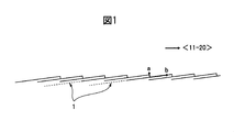
- FIG. 1 is a schematic view of a basal plane dislocation present in a SiC single crystal substrate, and the numeral 1 indicates the basal plane dislocation.
- the dislocation energy is smaller when the dislocation progresses in the epitaxial growth direction (a direction) than in the basal plane (b direction).
- the dislocation length is shortened), so that Burgers vectors are easily converted to equal edge dislocations.
- about 90 to 93% of the basal plane dislocation of the SiC single crystal substrate is converted into threading edge dislocation at the substrate / epitaxial film interface.
- the basal plane dislocation density in a 4 ° off substrate having an off angle of 4 ° with respect to the (0001) plane is about 4000 / cm 2, about 7 to 10% without conversion.
- the basal plane dislocation density remaining (take over) in the epitaxial film is about 280 to 400 / cm 2 .
- the size of the device electrode is currently about 2 to 3 mm square or more, at least 10 basal plane dislocations are contained in one device, which causes the device characteristics and yield to be degraded.
- An effective way to lower the basal plane dislocation density is to make the off-angle of the substrate smaller, but the number of steps present on the substrate is reduced, so the so-called step-flow growth is made during epitaxial growth. It becomes difficult to happen. As a result, the above-mentioned killer defects increase, which causes a problem of deterioration of device characteristics and yield.
- the conversion efficiency from basal plane dislocations to penetrating edge dislocations is further increased to reduce basal plane dislocations inherited from the substrate to the epitaxial growth layer. , And need to suppress the increase of killer defects.
- basal plane dislocations of the substrate are converted into threading edge dislocations by etching a SiC single crystal substrate with molten KOH and performing epitaxial growth thereon (see Non-Patent Document 3).
- Patent Document 1 At least one suppression layer formed of a silicon carbide single crystal thin film and having an Ra value of surface roughness of 0.5 nm or more and 1.0 nm or less is formed on a silicon carbide single crystal substrate to suppress generation of defects. Disclose how to Patent Document 1 discloses that setting the Ra value of the surface roughness within the above range increases the number of atoms taken into the step and promotes the step flow. However, Patent Document 1 does not disclose or suggest the relationship between etching of a silicon carbide single crystal substrate and reduction of basal plane dislocation. In addition, Patent Document 1 does not quantitatively evaluate the conversion rate at which basal plane dislocations are converted into threading edge dislocations.
- a buffer layer made of silicon carbide crystals is epitaxially grown on the surface of a hydrogen-etched silicon carbide single crystal substrate to form a buffer layer, and the surface of the buffer layer is subjected to hydrogen etching,
- a process is disclosed for epitaxially growing silicon carbide crystals on the surface of a buffer layer to form a finishing layer.
- the buffer layer forming step propagation of basal plane defects from the silicon carbide single crystal substrate is suppressed, and a finishing layer is formed on the surface of the hydrogen-etched buffer layer, thereby causing the silicon carbide single crystal substrate to be originated. It is disclosed that the propagation of basal plane dislocations can be further reduced, and a finish layer can be formed in which the defects caused by the buffer layer are also reduced.
- the manufacturing method disclosed in Patent Document 2 when the hydrogen etching of the buffer layer is omitted, the production yield of the semiconductor substrate may be lowered.
- the off angle in the off angle direction which is either the ⁇ 11-20> direction or the ⁇ 1-100> direction with respect to the (0001) plane, is 0.1 ° or more and 10 ° or less.
- a method of manufacturing a silicon carbide ingot in which a silicon carbide layer is formed on a base substrate made of crystalline silicon carbide is disclosed.
- Patent Document 3 does not disclose or suggest the relationship between the etching of the base substrate and the reduction of basal plane dislocation.
- Patent Document 3 does not quantitatively evaluate the conversion rate at which basal plane dislocations are converted into threading edge dislocations.
- the present invention provides an epitaxial SiC single crystal wafer having a high quality epitaxial film having a reduced basal plane dislocation remaining in an epitaxial growth layer even in epitaxial growth using a practical off angle SiC single crystal substrate.
- the present invention provides a method of manufacturing a SiC single crystal wafer.
- the present inventors epitaxially grow SiC on a SiC single crystal substrate by a thermal CVD method to manufacture an epitaxial SiC single crystal wafer, as described below. It has been found that the basal plane dislocation remaining in the inside can be reduced.
- the etching gas is flowed into the growth furnace to etch the SiC single crystal substrate before the epitaxial growth, and short step bunching starting from the basal plane dislocation is formed on the surface, thereby performing arithmetic on the surface of the SiC single crystal substrate.
- the average roughness Ra value is set to a predetermined value and then starting epitaxial growth
- basal plane dislocations on the surface of the SiC single crystal substrate can be effectively converted into threading edge dislocations.
- a predetermined buffer layer it is possible to further reduce the basal plane dislocation and to suppress the increase of the killer defect.
- the present inventors found and completed the present invention.
- the gist of the present invention is as follows. (1) A method of manufacturing an epitaxial silicon carbide single crystal wafer by epitaxially growing silicon carbide on a silicon carbide single crystal substrate by flowing a silicon-based material gas and a carbon-based material gas into an epitaxial growth furnace and using thermal CVD method Before starting the epitaxial growth, flow the etching gas into the epitaxial growth furnace to etch the surface of the silicon carbide single crystal substrate in advance so that the arithmetic average roughness Ra value becomes 0.5 nm or more and 3.0 nm or less. A method of manufacturing an epitaxial silicon carbide single crystal wafer characterized by the present invention.
- a silicon-based material gas and a carbon-based material gas are supplied into the epitaxial growth furnace, and silicon carbide is epitaxially grown on the surface of the etched silicon carbide single crystal substrate to form a buffer layer.
- the number of C atoms relative to the number of Si atoms of the silicon-based material gas and the carbon-based material gas when the buffer layer is formed.
- the growth temperature of 1600 ° C. or more and 1700 ° C.
- the silicon carbide single crystal substrate is characterized in that the off angle inclined in the ⁇ 11-20> direction with respect to the (0001) plane is 2 ° or more and 4 ° or less (1) to (5)
- the present invention it is possible to provide a high quality epitaxial SiC single crystal wafer with reduced basal plane dislocation remaining in an epitaxial film on a SiC single crystal substrate having a practical off angle of about 4 °, for example. It is possible. Further, in the manufacturing method of the present invention, since the CVD method is used, it is possible to obtain an epitaxial film having a simple apparatus configuration, excellent controllability, high uniformity, and high reproducibility. Furthermore, the device using the epitaxial SiC single crystal wafer of the present invention is formed on a high quality epitaxial film with reduced basal plane dislocation density, so that the characteristics and the yield are improved.
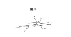
- FIG. 7A to 7C show that the method of the present invention promotes conversion of basal plane dislocations of a substrate to threading edge dislocations.
- FIG. 5 is a diagram showing a growth sequence of a SiC epitaxial film according to an example of the present invention.
- FIG. 7 is a view showing that the flatness of the buffer layer affects the conversion of basal plane dislocations of the SiC single crystal substrate into threading edge dislocations according to the present invention, and shows the case where the flatness of the buffer layer can not be maintained.
- FIG. 7 is a view showing that the flatness of the buffer layer affects the conversion of basal plane dislocations of the SiC single crystal substrate into threading edge dislocations according to the present invention, and shows the case where the flatness of the buffer layer is maintained.
- Optical micrograph showing the etch pits that appear when the surface of the epitaxial film is etched with molten KOH.
- An apparatus that can be suitably used for epitaxial growth in the method of manufacturing an epitaxial SiC single crystal wafer according to the present invention is a horizontal thermal CVD apparatus.
- the CVD method is a growth method excellent in controllability and reproducibility of an epitaxial film because the device configuration is simple and the growth can be controlled by on / off of gas.
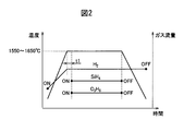
- FIG. 2 shows a typical growth sequence when performing conventional epitaxial film growth, together with the gas introduction timing.
- hydrogen gas is introduced to adjust the pressure to 5 k to 20 kPa. Thereafter, while maintaining the pressure constant, the hydrogen gas flow rate and the temperature of the growth furnace are raised, and after reaching the growth temperature of 1550 to 1650 ° C., the time of t1 in 100 to 200 liters per minute of hydrogen gas for 1 h Perform the etching.
- the purpose of this etching using hydrogen gas is to remove the oxide film formed on the surface of the SiC single crystal substrate, to remove the altered layer by processing, etc.
- the etching time (t1) is usually about 10 minutes. It is.
- the amount (thickness) of the SiC single crystal substrate etched at this time is about 10 to 50 nm, and the Ra value of the surface roughness of the SiC single crystal substrate after etching is about 0.1 to 0.2 nm .
- the surface roughness Ra represents the arithmetic mean roughness defined in JIS B0601-1994.
- the material gases SiH 4 and C 3 H 8 are introduced into the epitaxial growth furnace to start growth.
- the SiH 4 flow rate is 100 to 150 cm 3 / min
- the C 3 H 8 flow rate is 50 to 70 cm 3 / min (the ratio of the number of C atoms to the number of Si atoms in the material gas (C / Si ratio) is about 1 to 2)
- the growth rate is ⁇ 10 ⁇ m per hour. This growth rate is determined in consideration of productivity because the film thickness of the epitaxial layer that is usually used is about 10 ⁇ m.
- the film is grown for a predetermined time, and when the desired film thickness is obtained, the introduction of SiH 4 and C 3 H 8 is stopped, and the temperature is lowered in a state where only hydrogen gas flows. After the temperature drops to normal temperature, the introduction of hydrogen gas is stopped, the growth chamber is evacuated, the inert gas is introduced into the growth chamber, the growth chamber is returned to atmospheric pressure, and then the SiC single crystal substrate is taken out.
- Embodiment 1 (Etching process)
- the conditions for setting the SiC single crystal substrate in the epitaxial growth furnace and starting the etching of the surface of the SiC single crystal substrate are the same as the contents shown in FIG. Therefore, the etching gas used, the pressure conditions of the etching gas, the temperature at the time of etching, and the gas flow rate are the same as the conditions of the etching process in the prior art.
- the etching time t2 is set to about 0.5 to 1.5 hours so that short step bunching starting from basal plane dislocation is formed on the surface of the SiC single crystal substrate.
- the etching amount is about 500 nm to 1000 nm.
- This etching amount is an amount necessary to generate short step bunching shown below, and when too small, the step bunching density is insufficient and sufficient conversion efficiency of basal plane dislocation can not be obtained, and when too large, the surface is roughened. In this case, the conversion efficiency of the basal plane dislocation also decreases.
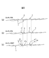
- FIG. 4 A photograph showing the appearance of the surface of the SiC single crystal substrate after etching is shown in FIG.
- a vertical line (line in the vertical direction of the drawing) of about 0.5 to 1 mm in length observed in FIG. 4 represents a short step bunching, and the portion of this line is convex. It has been confirmed that the basal plane dislocation of the SiC single crystal substrate exists at the center of this short step bunching, and the crystal state around the basal plane dislocation is changed, so that the progress of etching is delayed, and the basal plane It is considered that the portion around the plane dislocation has a convex shape. This situation is described in FIG.
- FIG. 5 (a) shows the same state as FIG. 1, and is a schematic cross-sectional view of the surface of the SiC single crystal substrate before etching or when etching is hardly performed as in the prior art.
- Reference numeral 1 is a basal plane dislocation of the SiC single crystal substrate
- reference numeral 2 is a step in which the crystalline state changes around the basal plane dislocation.
- step 2 The state in which the etching is in progress is schematically shown in FIG. Step 2 'in the vicinity of the surface exit of basal plane dislocation has a different crystalline state, so the amount of recession due to etching is small, and step 3 is a normal crystalline state in which no basal plane dislocation is present. The amount of retreat is also large.
- step 2 ′ FIG. 5B
- step 3 FIG. 5 (b) is etched and retreats to the position of step 2 ′ ′ after the etching of the step 2 ′ (symbol 3 ′ in FIG.
- the relationship between the etching time t2 in FIG. 3 and the surface roughness Ra value of the SiC single crystal substrate after etching in which short step bunching occurs can be determined in advance. Even if the etching time t2 is about 0.5 to 1.5 hours (hour) so that the Ra value is 0.5 nm or more and 3.0 nm or less based on the relationship between the etching time t2 and the surface roughness Ra value. good. By setting t2 to about 0.5 to 1.5 hours, the etching amount becomes 500 nm to 1000 nm, and the Ra at that time is 0.5 nm to 3.0 nm.
- the conversion efficiency of basal plane dislocation is the same as the case where the etching amount is not 500 nm or more and 1000 nm or less. It does not improve.
- epitaxial growth of SiC can be performed in the same procedure as in the case of FIG. 2.
- etching and performing epitaxial growth such that the surface roughness Ra value of the SiC single crystal substrate is 0.5 nm or more and 3.0 nm or less, a SiC single crystal having an off angle of about 4 °
- a good epitaxial film can be obtained in which the basal plane dislocation remaining in the film is reduced to 5% or less of the value in the SiC single crystal substrate.
- the basal plane dislocation easily proceeds in the direction a shown in FIG.
- the collective portion 10 of the steps formed in the vicinity of the basal plane dislocation by etching the SiC single crystal substrate more efficiently converts the basal plane dislocation of the SiC single crystal substrate into the threading edge dislocation,
- the fact that the Ra value of the surface is associated with the conversion efficiency is connected to the present invention, since it entails a short step bunching inevitably.
- the conversion rate at which basal plane dislocations are converted into threading edge dislocations can be 95% or more, as opposed to 90 to 93% in the prior art.
- the Ra value if the value is too small, such improvement in the conversion effect of dislocations is not observed, and if it is too large on the contrary, the terrace portion is also etched, so the dislocations are not converted. It is considered that the probability of progressing in the direction of the basal plane (direction b in FIG. 1) is increased, and there is an optimum value of Ra.
- the etching of the SiC single crystal substrate may be performed by flowing an etching gas into the epitaxial growth furnace, typically hydrogen gas can be used as the etching gas, and the etching is performed at a flow rate of about 100 to 200 L / min. You should do it.
- hydrogen gas for example, helium or argon may be used as the etching gas.
- the conditions in the growth furnace as shown in FIGS. 2 and 3 can be adopted for the temperature and pressure at the time of etching, and specifically, the temperature is 1500 ° C. or more and 1700 ° C. or less.
- the pressure is preferably 1 kPa to 20 kPa.
- Second Embodiment (Step of forming buffer layer)
- silicon-based and carbon-based material gases are flowed into the epitaxial growth furnace to epitaxially grow SiC, thereby forming a buffer layer and a device operation layer.
- the procedure for forming the V.sub.x will be described using the growth sequence of FIG. The process is the same as in FIG. 3 until the SiC single crystal substrate is set and the etching of the surface of the SiC single crystal substrate is completed.
- material gases SiH 4 and C 3 H 8 are introduced to start growth, but first, a buffer layer is formed and then a device operation layer is formed.
- This buffer layer mainly plays a role of promoting basal plane dislocation reduction by promoting conversion to threading edge dislocation, and a device operation layer is used for forming a device.
- the buffer layer By forming the buffer layer at the start of epitaxial growth as described above, in the epitaxial film after the device operation layer is grown, a favorable film in which basal plane dislocations remaining in the film are effectively reduced can be obtained. . This is because the epitaxial film is grown with a low C / Si ratio as a buffer layer, and an epitaxial film with high flatness is formed on the SiC single crystal substrate, as described in detail below. These basal plane dislocations are stably converted to threading edge dislocations. This will be described with reference to FIGS. 7A and 7B.
- FIG. 7A shows the case where the epitaxial layer 4 is grown at the same C / Si ratio as in the case where the device operation layer is formed on the SiC single crystal substrate after the etching is completed.
- the portion 2 ′ ′ where short step bunching occurs in the vicinity of the basal plane dislocation 1 of the above step flow growth is difficult to progress because the crystal state is disordered.
- the film thickness increases particularly at the initial stage of growth, and the edge portion swells as shown by the reference numeral 5, and conversely, the film thickness decreases at the lower portion 6 like a foot.
- the basal plane dislocation 1 of the SiC single crystal substrate becomes shorter in the b direction, so the basal plane dislocation remains as it is in the epitaxial film and etching before growth The effect of optimizing is reduced.
- the surface Ra value is over 3 nm.
- the C / Si ratio is low. It is important to form the epitaxial film 4 with high flatness as a buffer layer.
- the surface Ra value of the buffer layer in this case is 1 to 3 nm.
- the thickness of the buffer layer grown on the SiC single crystal substrate after completion of etching is 0.5 ⁇ m or more so that conversion of basal plane dislocation of the SiC single crystal substrate on which short step bunching is formed by etching can be completed. It is 1 ⁇ m or less. Since this buffer layer grows at a low C / Si ratio, the growth time becomes longer as it becomes thicker, and the upper limit of the film thickness is taken into consideration that the stability of the grown film becomes a problem due to the fluctuation of the C / Si ratio. It is decided.
- the ratio of the number of C atoms to the number of Si atoms in the material gas (C / Si ratio) at the time of growing the buffer layer is 0.3 or more and 0.6 or less. As described above, this is necessary to promote step flow growth, and if it is larger than 0.6, the effect becomes small, and if smaller than 0.3, generation of Si droplets becomes a problem.
- the SiH 4 is used as a material gas of silicon series, when using the C 3 H 8 as a material gas of carbon-based, SiH 4 flow rate for growing the buffer layer is min 50 ⁇ 60cm 3, C 3 H Eight flow rates are 6 to 10 cm 3 per minute.
- the quality of the film is lowered if it is less than 1600 ° C., and the reevaporation of atoms from the surface becomes large if it exceeds 1700 ° C.
- the temperature is higher than or equal to 1600 ° C. and lower than or equal to 1700 ° C.
- the pressure at the time of growth also affects the quality of the film, and if it is too low, the surface roughness increases, and if it is too high, the generation of Si droplets becomes a problem, so the pressure when forming the buffer layer is 2 kPa or more and 10 kPa or less I assume.
- the device operation layer is grown under growth conditions according to the application of the device used.
- C is higher than C / Si of the silicon-based material gas and the carbon-based material gas when the buffer layer is formed without the step of etching the buffer layer between the buffer layer forming step and the device operation layer.
- silicon-based material gas and carbon-based material gas are flowed to epitaxially grow silicon carbide directly on the buffer layer to form a device operation layer.
- the ratio of the number of C atoms to the number of Si atoms in the material gas is preferably 1.0 or more and 2.0 or less, and the growth temperature is 1600 ° C. or more and 1700 ° C. or less
- the growth pressure is preferably 2 kPa to 10 kPa.
- the thickness of the device operation layer can also be appropriately set depending on the application etc., but is preferably 5 ⁇ m or more and 50 ⁇ m or less.
- the material gas is not limited to these, and, for example, a silicon-based material SiHCl 3 , SiH 2 Cl 2 , SiCl 4 or the like can be used as the gas, or C 2 H 4 , CH 4 or the like can be used as the carbon-based material gas.
- a doping gas such as N 2 may be flowed together.
- the off-angle inclined in the ⁇ 11-20> direction with respect to the (0001) plane is 2 ° or more and 4 ° or less.
- the off angle is larger than 4 °, the angle at which the basal plane dislocation in the substrate intersects the off angled surface becomes large, and it is perpendicular to that in the direction of the basal plane (direction b in FIG. 1) during epitaxial growth.
- the effect of the present invention is difficult to appear because the length of dislocations does not change much even if it proceeds to the a direction in 1).
- it is smaller than 2 ° the number of basal plane dislocations in the initial state is small, and adverse effects such as inhibition of step flow growth due to the terrace being too wide become large.
- the device suitably formed on the epitaxial SiC single crystal wafer grown in this manner is not particularly limited, and examples thereof include a Schottky barrier diode, a PIN diode, a MOS diode, and a MOS transistor. However, it is suitable to obtain a device used for power control.
- This SiC single crystal substrate has an off angle of 4 ° in the ⁇ 11-20> direction with respect to the (0001) plane.
- the growth sequence is as shown in the growth sequence of FIG. 6. Specifically, after setting the SiC single crystal substrate in the epitaxial growth furnace and evacuating the growth furnace, the pressure is set to 10 kPa while introducing hydrogen gas. It was adjusted. Thereafter, while maintaining the pressure constant, the flow rate of hydrogen gas and the temperature of the growth reactor were increased, and finally the hydrogen gas was 150 L / min and the temperature of the growth reactor was 1635 ° C. Thereafter, the pressure was adjusted to 2 kPa and etching of the SiC single crystal substrate was performed for 40 minutes in hydrogen gas.
- the surface roughness Ra of the SiC single crystal substrate after this etching is 0.5 nm.
- the growth furnace temperature is increased to 1650 ° C.
- SiH 4 flow rate is 150 cm 3 / min
- C 3 H 8 flow rate is 65 cm 3 / min
- growth is started, and the epitaxial layer is grown to a thickness of 10 ⁇ m. (C / Si ratio is 1.3).
- the grown epitaxial layer is a device operation layer for device operation, and a buffer layer for further increasing the conversion efficiency of basal plane dislocations is not grown.
- the film epitaxially grown in this manner is etched with molten KOH, and an optical micrograph of the surface of the device operation layer where an etch pit appears is shown in FIG. Arrows in the photograph of FIG. 8 are etch pits due to basal plane dislocation, and the other pits are due to threading screw dislocations or threading edge dislocations.
- the basal plane dislocation density in the obtained epitaxial film was evaluated by such a method, and compared with the basal plane dislocation density of the SiC single crystal substrate.
- the basal plane of the surface of the SiC single crystal substrate Dislocations inherited to the epitaxial film accounted for 3.5% of the total. That is, 96.5% of basal plane dislocations on the surface of the SiC single crystal substrate were converted, and it is considered that these were converted to threading edge dislocations.
- Tables 1 and 2 summarize the growth conditions and conversion efficiency of the epitaxial film.
- Reference Example 2 The epitaxial growth was performed on the Si surface of a 4-inch (100 mm) SiC single crystal substrate having a 4H-type polytype, which was sliced, roughly cut, and polished in the same manner as in Reference Example 1.
- the off angle of the SiC single crystal substrate is 4 ° (the off direction is the same as in the first embodiment).
- the process up to the start of etching in hydrogen gas is the same as in Example 1.
- the etching time is 60 minutes, and the surface roughness Ra value of the SiC single crystal substrate after etching is 1.3 nm. I made it.
- epitaxial growth was performed in the same manner as in Reference Example 1 (no formation of a buffer layer).
- the epitaxial film after growth was etched with molten KOH and the dislocation density was evaluated by the etch pit.
- the conversion of basal plane dislocation on the surface of the SiC single crystal substrate was 97%.
- Reference Example 4 The epitaxial growth was performed on the Si surface of a 4-inch (100 mm) SiC single crystal substrate having a 4H-type polytype, which was sliced, roughly cut, and polished in the same manner as in Reference Example 1. Except that the off angle of the SiC single crystal substrate is 2 °, the etching with hydrogen gas, the Ra value of the SiC single crystal substrate after etching, and the conditions for epitaxial growth are the same as those of Reference Example 1 (formation of buffer layer is None). The epitaxial film after growth was etched with molten KOH, and the dislocation density was evaluated by the etch pit. The conversion of basal plane dislocation on the surface of the SiC single crystal substrate was 96%.
- Example 1 The epitaxial growth was performed on the Si surface of a 4-inch (100 mm) SiC single crystal substrate having a 4H-type polytype, which was sliced, roughly cut, and polished in the same manner as in Reference Example 1.
- the off angle of the SiC single crystal substrate is 4 ° (the off direction is the same as in the first embodiment).
- the etching with hydrogen gas and the Ra value of the SiC single crystal substrate after etching are the same as in the first reference example.
- the temperature of the growth furnace was raised to 1650 ° C. to grow a buffer layer.
- the growth conditions are: SiH 4 flow rate 50 cm 3 / min, C 3 H 8 flow rate 6.7 cm 3 / min (C / Si ratio 0.4), growth pressure 6 kPa, 0.5 ⁇ m thick SiC epitaxial film I got
- epitaxial layer for device operation with SiH 4 flow rate 150 cm 3 / min, C 3 H 8 flow rate 65 cm 3 / min (C / Si ratio 1.3) and pressure 2 kPa (Device operation layer) was grown to 10 ⁇ m. Then, the epitaxial film after growth was etched with molten KOH, and the dislocation density was evaluated by the etch pit. As a result, the conversion ratio of basal plane dislocation on the surface of the SiC single crystal substrate was 98.5%.
- Example 2 The epitaxial growth was performed on the Si surface of a 4-inch (100 mm) SiC single crystal substrate having a 4H-type polytype, which was sliced, roughly cut, and polished in the same manner as in Reference Example 1.
- the off angle of the SiC single crystal substrate is 4 ° (the off direction is the same as in the first embodiment).
- the etching with hydrogen gas and the Ra value of the SiC single crystal substrate after the etching are the same as in the reference example 2. After etching, the temperature of the growth furnace was raised to 1650 ° C. to grow a buffer layer.
- the growth conditions are SiH 4 flow rate 50 cm 3 / min, C 3 H 8 flow rate 5 cm 3 / min (C / Si ratio 0.3), growth pressure 6 kPa, and a 0.8 ⁇ m thick SiC epitaxial film is obtained.
- epitaxial layer for device operation with SiH 4 flow rate 150 cm 3 / min, C 3 H 8 flow rate 65 cm 3 / min (C / Si ratio 1.3) and pressure 2 kPa (Device operation layer) was grown to 10 ⁇ m. Then, the epitaxial film after growth was etched with molten KOH, and the dislocation density was evaluated by the etch pit. As a result, the conversion ratio of basal plane dislocation on the surface of the SiC single crystal substrate was 98%.
- Example 3 The epitaxial growth was performed on the Si surface of a 4-inch (100 mm) SiC single crystal substrate having a 4H-type polytype, which was sliced, roughly cut, and polished in the same manner as in Reference Example 1.
- the off angle of the SiC single crystal substrate is 4 ° (the off direction is the same as in the first embodiment).
- the etching with hydrogen gas and the Ra value of the SiC single crystal substrate after etching are the same as in the third embodiment. After etching, the temperature of the growth furnace was raised to 1650 ° C. to grow a buffer layer.
- the growth conditions were a SiH 4 flow rate of 50 cm 3 / min, a C 3 H 8 flow rate of 10 cm 3 / min (C / Si ratio of 0.6), and a growth pressure of 6 kPa to obtain a 1 ⁇ m thick SiC epitaxial film.
- epitaxial layer for device operation with SiH 4 flow rate 150 cm 3 / min, C 3 H 8 flow rate 65 cm 3 / min (C / Si ratio 1.3) and pressure 2 kPa (Device operation layer) was grown to 10 ⁇ m.
- the epitaxial film after growth was etched with molten KOH and the dislocation density was evaluated by the etch pit. The conversion of basal plane dislocation on the surface of the SiC single crystal substrate was 97.8%.
- Example 4 The epitaxial growth was performed on the Si surface of a 4-inch (100 mm) SiC single crystal substrate having a 4H-type polytype, which was sliced, roughly cut, and polished in the same manner as in Reference Example 1. Etching and epitaxial film growth were performed in the same manner as in Example 1 except that the off angle of the SiC single crystal substrate was 2 °. The epitaxial film after growth was etched with molten KOH and the dislocation density was evaluated by the etch pit. The conversion of basal plane dislocation on the surface of the SiC single crystal substrate was 97.5%.
- the epitaxial growth was performed on the Si surface of a 4-inch (100 mm) SiC single crystal substrate having a 4H-type polytype, which was sliced, roughly cut, and polished in the same manner as in Reference Example 1.
- the off angle of the SiC single crystal substrate is 4 ° (the off direction is the same as in the first embodiment).
- the etching time is 10 minutes, and the surface roughness Ra of the SiC single crystal substrate after etching is 0.2 nm.
- epitaxial growth was performed in the same manner as in Reference Example 1 (no formation of a buffer layer).
- the epitaxial film after growth was etched with molten KOH, and the dislocation density was evaluated by the etch pit.
- the conversion ratio of basal plane dislocation on the surface of the SiC single crystal substrate is 91%, and the conversion efficiency is compared to the reference example. It was falling.
- the growth conditions are as follows: SiH 4 flow rate is 50 cm 3 / min, C 3 H 8 flow rate is 6.7 cm 3 / min (C / Si ratio is 0.4), growth pressure is 6 kPa, and a 2 ⁇ m-thick SiC epitaxial film is obtained.
- the epitaxial layer for device operation (Si / Si flow rate 150 cm 3 / min, C 3 H 8 flow rate 65 cm 3 / min (C / Si ratio 1.3) and pressure 2 kPa
- the device operation layer was grown to 10 ⁇ m.
- the epitaxial film after growth was etched with molten KOH and the dislocation density was evaluated by the etch pit.
- the conversion of basal plane dislocation on the surface of the SiC single crystal substrate was 93%. This is considered to be because the film thickness of the buffer layer is large and the growth time is long, so that the flatness of the film is deteriorated due to the fluctuation of the C / Si ratio, and the conversion efficiency is lowered.
- the temperature of the growth furnace is lowered to 1650 ° C.
- the SiH 4 flow rate is 150 cm 3 / min
- the C 3 H 8 flow rate is 65 cm 3 / min (C / Si ratio is 1.3)
- the pressure is At 2 kPa
- an epitaxial layer (device operation layer) for device operation was grown to 10 ⁇ m.
- the epitaxial film after growth was etched with molten KOH and the dislocation density was evaluated by the etch pit.
- the conversion of basal plane dislocation on the surface of the SiC single crystal substrate was 90.5%. It is considered that this is because the buffer layer is grown at a high temperature, so re-evaporation of atoms from the surface is large, the flatness of the film is deteriorated, and the conversion efficiency is lowered.
- the growth conditions are: SiH 4 flow rate is 50 cm 3 / min, C 3 H 8 flow rate is 6.7 cm 3 / min (C / Si ratio is 0.4), growth pressure is 1.5 kPa, and 0.5 ⁇ m thick SiC An epitaxial film was obtained.
- the epitaxial layer for device operation (Si / Si flow rate 150 cm 3 / min, C 3 H 8 flow rate 65 cm 3 / min (C / Si ratio 1.3) and pressure 2 kPa
- the device operation layer was grown to 10 ⁇ m.
- the epitaxial film after growth was etched with molten KOH and the dislocation density was evaluated by the etch pit.
- the conversion of basal plane dislocation on the surface of the SiC single crystal substrate was 91%. It is considered that this is because the surface of the buffer layer is roughened by growing the buffer layer under a low pressure, the flatness of the film is deteriorated, and the conversion efficiency is lowered.
- Tables 1 and 2 show the conditions and evaluation results of Reference Examples 1 to 4 and Examples 1 to 4 and Comparative Examples 1 to 8.
- the present invention in epitaxial growth on a SiC single crystal substrate, it is possible to produce an epitaxial SiC single crystal wafer having a high quality epitaxial film with few basal plane dislocations. Therefore, if an electronic device is formed on such an epitaxial SiC single crystal wafer, it can be expected that the characteristics and yield of the device will be improved.
Landscapes
- Engineering & Computer Science (AREA)
- Chemical & Material Sciences (AREA)
- Power Engineering (AREA)
- Microelectronics & Electronic Packaging (AREA)
- Physics & Mathematics (AREA)
- Condensed Matter Physics & Semiconductors (AREA)
- General Physics & Mathematics (AREA)
- Computer Hardware Design (AREA)
- Manufacturing & Machinery (AREA)
- Crystallography & Structural Chemistry (AREA)
- Materials Engineering (AREA)
- Metallurgy (AREA)
- Organic Chemistry (AREA)
- Chemical Kinetics & Catalysis (AREA)
- General Chemical & Material Sciences (AREA)
- Inorganic Chemistry (AREA)
- Ceramic Engineering (AREA)
- Plasma & Fusion (AREA)
- Crystals, And After-Treatments Of Crystals (AREA)
- Chemical Vapour Deposition (AREA)
Abstract
Priority Applications (5)
| Application Number | Priority Date | Filing Date | Title |
|---|---|---|---|
| US15/747,849 US10626520B2 (en) | 2015-07-29 | 2016-07-29 | Method for producing epitaxial silicon carbide single crystal wafer |
| JP2017530950A JP6524233B2 (ja) | 2015-07-29 | 2016-07-29 | エピタキシャル炭化珪素単結晶ウェハの製造方法 |
| CN201680033576.5A CN107709635B (zh) | 2015-07-29 | 2016-07-29 | 外延碳化硅单晶晶片的制造方法 |
| EP16830636.3A EP3330415A4 (fr) | 2015-07-29 | 2016-07-29 | Procédé de production de plaquette de monocristal de carbure de silicium épitaxiale |
| KR1020187000978A KR102106722B1 (ko) | 2015-07-29 | 2016-07-29 | 에피택셜 탄화규소 단결정 웨이퍼의 제조 방법 |
Applications Claiming Priority (2)
| Application Number | Priority Date | Filing Date | Title |
|---|---|---|---|
| JP2015-149742 | 2015-07-29 | ||
| JP2015149742 | 2015-07-29 |
Publications (1)
| Publication Number | Publication Date |
|---|---|
| WO2017018533A1 true WO2017018533A1 (fr) | 2017-02-02 |
Family
ID=57884506
Family Applications (1)
| Application Number | Title | Priority Date | Filing Date |
|---|---|---|---|
| PCT/JP2016/072421 WO2017018533A1 (fr) | 2015-07-29 | 2016-07-29 | Procédé de production de plaquette de monocristal de carbure de silicium épitaxiale |
Country Status (6)
| Country | Link |
|---|---|
| US (1) | US10626520B2 (fr) |
| EP (1) | EP3330415A4 (fr) |
| JP (1) | JP6524233B2 (fr) |
| KR (1) | KR102106722B1 (fr) |
| CN (1) | CN107709635B (fr) |
| WO (1) | WO2017018533A1 (fr) |
Cited By (5)
| Publication number | Priority date | Publication date | Assignee | Title |
|---|---|---|---|---|
| WO2018123148A1 (fr) * | 2016-12-27 | 2018-07-05 | 住友電気工業株式会社 | Substrat épitaxique au carbure de silicium et procédé de production d'un dispositif semi-conducteur au carbure de silicium |
| WO2018174105A1 (fr) * | 2017-03-22 | 2018-09-27 | 東洋炭素株式会社 | Procédé de fabrication de tranche de sic reformé, tranche de sic fixée à une couche épitaxiale, son procédé de fabrication, et procédé de traitement de surface |
| WO2020095872A1 (fr) * | 2018-11-05 | 2020-05-14 | 学校法人関西学院 | Substrat semi-conducteur en sic, son procédé et son dispositif de fabrication |
| WO2021025086A1 (fr) * | 2019-08-06 | 2021-02-11 | 学校法人関西学院 | PROCÉDÉ DE FABRICATION DE SUBSTRAT EN SiC |
| WO2021060369A1 (fr) * | 2019-09-27 | 2021-04-01 | 学校法人関西学院 | Substrat sic, procédé de production de substrat sic, dispositif à semi-conducteurs sic et procédé de production de dispositif à semi-conducteurs sic |
Families Citing this family (11)
| Publication number | Priority date | Publication date | Assignee | Title |
|---|---|---|---|---|
| CN109791879B (zh) * | 2016-10-04 | 2023-07-25 | 住友电气工业株式会社 | 碳化硅外延衬底和制造碳化硅半导体器件的方法 |
| JP2020170816A (ja) * | 2019-04-05 | 2020-10-15 | 三菱電機株式会社 | 炭化珪素エピタキシャルウエハ、炭化珪素エピタキシャルウエハの製造方法、電力変換装置 |
| EP3967793A4 (fr) * | 2019-05-10 | 2023-01-11 | Adamant Namiki Precision Jewel Co., Ltd. | Substrat de cristal de diamant et procédé de production de substrat de cristal de diamant |
| WO2021025085A1 (fr) * | 2019-08-06 | 2021-02-11 | 学校法人関西学院 | SUBSTRAT SiC, SUBSTRAT ÉPITAXIAL SiC, LINGOT DE SiC ET SES PROCÉDÉS DE PRODUCTION |
| WO2021025084A1 (fr) * | 2019-08-06 | 2021-02-11 | 学校法人関西学院 | GERME CRISTALLIN DE SiC ET SON PROCÉDÉ DE PRODUCTION, LINGOT DE SiC PRODUIT PAR LA MISE EN CROISSANCE DUDIT GERME CRISTALLIN DE SiC ET SON PROCÉDÉ DE PRODUCTION, ET TRANCHE DE SiC PRODUITE À PARTIR DUDIT LINGOT DE SiC ET TRANCHE DE SiC À FILM ÉPITAXIAL ET PROCÉDÉS RESPECTIFS DE PRODUCTION DE LADITE TRANCHE DE SiC ET DE LADITE TRANCHE DE SiC À FILM ÉPITAXIAL |
| CN112420803A (zh) * | 2019-08-23 | 2021-02-26 | 比亚迪股份有限公司 | 碳化硅衬底及其制备方法和半导体器件 |
| CN111029278B (zh) * | 2019-12-10 | 2021-06-29 | 长江存储科技有限责任公司 | 一种晶圆片的加工方法和系统 |
| JP7319502B2 (ja) * | 2020-01-09 | 2023-08-02 | 株式会社東芝 | 炭化珪素基体の製造方法、半導体装置の製造方法、炭化珪素基体、及び、半導体装置 |
| EP4130349A4 (fr) * | 2020-05-06 | 2023-10-18 | Meishan Boya Advanced Materials Co., Ltd. | Appareil de préparation de cristal et procédé de croissance de cristal |
| JP2022020995A (ja) * | 2020-07-21 | 2022-02-02 | 三菱電機株式会社 | 炭化珪素エピタキシャルウエハの製造方法 |
| KR102434780B1 (ko) | 2021-06-17 | 2022-08-22 | 주식회사 쎄닉 | 탄화규소 웨이퍼 및 반도체 소자 |
Citations (4)
| Publication number | Priority date | Publication date | Assignee | Title |
|---|---|---|---|---|
| JP2009256138A (ja) * | 2008-04-17 | 2009-11-05 | Nippon Steel Corp | エピタキシャル炭化珪素単結晶基板及びその製造方法 |
| US20140117380A1 (en) * | 2012-10-26 | 2014-05-01 | Dow Corning Corporation | Flat sic semiconductor substrate |
| WO2014125550A1 (fr) * | 2013-02-13 | 2014-08-21 | 三菱電機株式会社 | Procédé de fabrication de tranche épitaxiale en sic |
| JP2015000824A (ja) * | 2013-06-13 | 2015-01-05 | 東洋炭素株式会社 | 単結晶SiC基板の表面処理方法及び単結晶SiC基板 |
Family Cites Families (22)
| Publication number | Priority date | Publication date | Assignee | Title |
|---|---|---|---|---|
| JP4954654B2 (ja) | 2006-09-21 | 2012-06-20 | 新日本製鐵株式会社 | エピタキシャル炭化珪素単結晶基板及びその製造方法 |
| TWI408262B (zh) * | 2007-09-12 | 2013-09-11 | Showa Denko Kk | 磊晶SiC單晶基板及磊晶SiC單晶基板之製造方法 |
| JP5504597B2 (ja) * | 2007-12-11 | 2014-05-28 | 住友電気工業株式会社 | 炭化ケイ素半導体装置およびその製造方法 |
| JP2009218575A (ja) | 2008-02-12 | 2009-09-24 | Toyota Motor Corp | 半導体基板の製造方法 |
| JP5516424B2 (ja) * | 2009-02-04 | 2014-06-11 | 日立金属株式会社 | エピタキシャル成長用炭化珪素単結晶基板の製造方法 |
| US9464366B2 (en) * | 2009-08-20 | 2016-10-11 | The United States Of America, As Represented By The Secretary Of The Navy | Reduction of basal plane dislocations in epitaxial SiC |
| JP4959763B2 (ja) * | 2009-08-28 | 2012-06-27 | 昭和電工株式会社 | SiCエピタキシャルウェハ及びその製造方法 |
| JP4887418B2 (ja) | 2009-12-14 | 2012-02-29 | 昭和電工株式会社 | SiCエピタキシャルウェハの製造方法 |
| EP2642001B1 (fr) * | 2010-11-17 | 2020-10-21 | Showa Denko K.K. | Procédé de fabrication d'un substrat monocristallin de carbure de silicium épitaxial |
| US8722507B2 (en) * | 2011-01-06 | 2014-05-13 | Hitachi Metals, Ltd. | Method for forming identification marks on silicon carbide single crystal substrate, and silicon carbide single crystal substrate |
| JP5803265B2 (ja) | 2011-05-20 | 2015-11-04 | 住友電気工業株式会社 | 炭化珪素基板および炭化珪素インゴットの製造方法 |
| JP5961357B2 (ja) * | 2011-09-09 | 2016-08-02 | 昭和電工株式会社 | SiCエピタキシャルウェハ及びその製造方法 |
| US20130062628A1 (en) * | 2011-09-10 | 2013-03-14 | Semisouth Laboratories, Inc. | Methods for the epitaxial growth of silicon carbide |
| US9885124B2 (en) * | 2011-11-23 | 2018-02-06 | University Of South Carolina | Method of growing high quality, thick SiC epitaxial films by eliminating silicon gas phase nucleation and suppressing parasitic deposition |
| JP5865777B2 (ja) * | 2012-05-16 | 2016-02-17 | 三菱電機株式会社 | 炭化珪素エピタキシャルウェハの製造方法 |
| TWI600081B (zh) | 2012-11-16 | 2017-09-21 | Toyo Tanso Co Ltd | Surface treatment method of single crystal silicon carbide substrate and single crystal silicon carbide substrate |
| JP2014154666A (ja) * | 2013-02-07 | 2014-08-25 | Sumitomo Electric Ind Ltd | 炭化珪素半導体基板の製造方法および炭化珪素半導体装置の製造方法 |
| WO2014150400A1 (fr) | 2013-03-15 | 2014-09-25 | The Government Of The United States Of America, As Represented By The Secretary Of The Navy | Réduction des dislocations dans le plan basal dans du sic épitaxial au moyen d'un procédé de gravure in situ |
| KR101885975B1 (ko) * | 2014-02-28 | 2018-08-06 | 쇼와 덴코 가부시키가이샤 | 에피택셜 탄화규소 웨이퍼의 제조 방법 |
| JP6311384B2 (ja) * | 2014-03-24 | 2018-04-18 | 三菱電機株式会社 | 炭化珪素半導体装置の製造方法 |
| KR101947926B1 (ko) * | 2014-07-16 | 2019-02-13 | 쇼와 덴코 가부시키가이샤 | 에피택셜 탄화규소 웨이퍼의 제조 방법 |
| US10727047B2 (en) * | 2015-02-18 | 2020-07-28 | Showa Denko K.K. | Epitaxial silicon carbide single crystal wafer and process for producing the same |
-
2016
- 2016-07-29 EP EP16830636.3A patent/EP3330415A4/fr active Pending
- 2016-07-29 CN CN201680033576.5A patent/CN107709635B/zh active Active
- 2016-07-29 WO PCT/JP2016/072421 patent/WO2017018533A1/fr active Application Filing
- 2016-07-29 US US15/747,849 patent/US10626520B2/en active Active
- 2016-07-29 KR KR1020187000978A patent/KR102106722B1/ko active IP Right Grant
- 2016-07-29 JP JP2017530950A patent/JP6524233B2/ja active Active
Patent Citations (4)
| Publication number | Priority date | Publication date | Assignee | Title |
|---|---|---|---|---|
| JP2009256138A (ja) * | 2008-04-17 | 2009-11-05 | Nippon Steel Corp | エピタキシャル炭化珪素単結晶基板及びその製造方法 |
| US20140117380A1 (en) * | 2012-10-26 | 2014-05-01 | Dow Corning Corporation | Flat sic semiconductor substrate |
| WO2014125550A1 (fr) * | 2013-02-13 | 2014-08-21 | 三菱電機株式会社 | Procédé de fabrication de tranche épitaxiale en sic |
| JP2015000824A (ja) * | 2013-06-13 | 2015-01-05 | 東洋炭素株式会社 | 単結晶SiC基板の表面処理方法及び単結晶SiC基板 |
Non-Patent Citations (1)
| Title |
|---|
| See also references of EP3330415A4 * |
Cited By (18)
| Publication number | Priority date | Publication date | Assignee | Title |
|---|---|---|---|---|
| WO2018123148A1 (fr) * | 2016-12-27 | 2018-07-05 | 住友電気工業株式会社 | Substrat épitaxique au carbure de silicium et procédé de production d'un dispositif semi-conducteur au carbure de silicium |
| WO2018174105A1 (fr) * | 2017-03-22 | 2018-09-27 | 東洋炭素株式会社 | Procédé de fabrication de tranche de sic reformé, tranche de sic fixée à une couche épitaxiale, son procédé de fabrication, et procédé de traitement de surface |
| CN110431654A (zh) * | 2017-03-22 | 2019-11-08 | 东洋炭素株式会社 | 改性SiC晶片的制造方法、附有外延层的SiC晶片、其制造方法、及表面处理方法 |
| KR20190129104A (ko) * | 2017-03-22 | 2019-11-19 | 토요 탄소 가부시키가이샤 | 개질 SiC 웨이퍼의 제조 방법, 에피택셜층 부착 SiC 웨이퍼, 그의 제조 방법, 및 표면 처리 방법 |
| JPWO2018174105A1 (ja) * | 2017-03-22 | 2020-01-30 | 東洋炭素株式会社 | 改質SiCウエハの製造方法、エピタキシャル層付きSiCウエハ、その製造方法、及び表面処理方法 |
| KR102604446B1 (ko) | 2017-03-22 | 2023-11-22 | 토요타 쯔우쇼우 가부시키가이샤 | 개질 SiC 웨이퍼의 제조 방법, 에피택셜층 부착 SiC 웨이퍼, 그의 제조 방법, 및 표면 처리 방법 |
| US11261539B2 (en) | 2017-03-22 | 2022-03-01 | Toyo Tanso Co., Ltd. | Method for manufacturing reformed sic wafer, epitaxial layer-attached sic wafer, method for manufacturing same, and surface treatment method |
| JP7008063B2 (ja) | 2017-03-22 | 2022-01-25 | 東洋炭素株式会社 | 改質SiCウエハの製造方法及びエピタキシャル層付きSiCウエハの製造方法 |
| CN113227465A (zh) * | 2018-11-05 | 2021-08-06 | 学校法人关西学院 | SiC半导体衬底及其制造方法和制造装置 |
| JPWO2020095872A1 (ja) * | 2018-11-05 | 2021-09-24 | 学校法人関西学院 | SiC半導体基板及びその製造方法及びその製造装置 |
| JP7278550B2 (ja) | 2018-11-05 | 2023-05-22 | 学校法人関西学院 | SiC半導体基板及びその製造方法及びその製造装置 |
| WO2020095872A1 (fr) * | 2018-11-05 | 2020-05-14 | 学校法人関西学院 | Substrat semi-conducteur en sic, son procédé et son dispositif de fabrication |
| CN113227465B (zh) * | 2018-11-05 | 2024-03-29 | 学校法人关西学院 | SiC半导体衬底及其制造方法和制造装置 |
| US12020928B2 (en) | 2018-11-05 | 2024-06-25 | Kwansei Gakuin Educational Foundation | SiC semiconductor substrate, method for manufacturing same, and device for manufacturing same |
| WO2021025086A1 (fr) * | 2019-08-06 | 2021-02-11 | 学校法人関西学院 | PROCÉDÉ DE FABRICATION DE SUBSTRAT EN SiC |
| US20220290324A1 (en) * | 2019-08-06 | 2022-09-15 | Kwansei Gakuin Educational Foundation | SiC SUBSTRATE PRODUCTION METHOD |
| US12098476B2 (en) * | 2019-08-06 | 2024-09-24 | Kwansei Gakuin Educational Foundation | Method for producing a SiC substrate via an etching step, growth step, and peeling step |
| WO2021060369A1 (fr) * | 2019-09-27 | 2021-04-01 | 学校法人関西学院 | Substrat sic, procédé de production de substrat sic, dispositif à semi-conducteurs sic et procédé de production de dispositif à semi-conducteurs sic |
Also Published As
| Publication number | Publication date |
|---|---|
| KR20180016585A (ko) | 2018-02-14 |
| US10626520B2 (en) | 2020-04-21 |
| KR102106722B1 (ko) | 2020-05-04 |
| US20180216251A1 (en) | 2018-08-02 |
| EP3330415A1 (fr) | 2018-06-06 |
| CN107709635B (zh) | 2021-02-26 |
| EP3330415A4 (fr) | 2019-03-20 |
| JP6524233B2 (ja) | 2019-06-05 |
| JPWO2017018533A1 (ja) | 2018-05-10 |
| CN107709635A (zh) | 2018-02-16 |
Similar Documents
| Publication | Publication Date | Title |
|---|---|---|
| JP6524233B2 (ja) | エピタキシャル炭化珪素単結晶ウェハの製造方法 | |
| JP4850960B2 (ja) | エピタキシャル炭化珪素単結晶基板の製造方法 | |
| JP4987792B2 (ja) | エピタキシャル炭化珪素単結晶基板の製造方法 | |
| JP4954654B2 (ja) | エピタキシャル炭化珪素単結晶基板及びその製造方法 | |
| JP4842094B2 (ja) | エピタキシャル炭化珪素単結晶基板の製造方法 | |
| JP6742477B2 (ja) | エピタキシャル炭化珪素単結晶ウエハの製造方法及びエピタキシャル炭化珪素単結晶ウエハ | |
| JP2017031050A (ja) | エピタキシャル炭化珪素ウエハ用炭化珪素単結晶基板の製造方法及びエピタキシャル炭化珪素ウエハ用炭化珪素単結晶基板 | |
| JP6304699B2 (ja) | エピタキシャル炭化珪素ウエハの製造方法 | |
| JP5786759B2 (ja) | エピタキシャル炭化珪素ウエハの製造方法 | |
| JP5664534B2 (ja) | エピタキシャル炭化珪素ウエハの製造方法 | |
| US9957639B2 (en) | Method for producing epitaxial silicon carbide wafer | |
| JP6628673B2 (ja) | エピタキシャル炭化珪素単結晶ウェハの製造方法 | |
| JP2017100911A (ja) | エピタキシャル炭化珪素単結晶ウェハの製造方法 |
Legal Events
| Date | Code | Title | Description |
|---|---|---|---|
| 121 | Ep: the epo has been informed by wipo that ep was designated in this application |
Ref document number: 16830636 Country of ref document: EP Kind code of ref document: A1 |
|
| ENP | Entry into the national phase |
Ref document number: 20187000978 Country of ref document: KR Kind code of ref document: A |
|
| ENP | Entry into the national phase |
Ref document number: 2017530950 Country of ref document: JP Kind code of ref document: A |
|
| WWE | Wipo information: entry into national phase |
Ref document number: 15747849 Country of ref document: US |
|
| NENP | Non-entry into the national phase |
Ref country code: DE |
|
| WWE | Wipo information: entry into national phase |
Ref document number: 2016830636 Country of ref document: EP |