WO2021025084A1 - GERME CRISTALLIN DE SiC ET SON PROCÉDÉ DE PRODUCTION, LINGOT DE SiC PRODUIT PAR LA MISE EN CROISSANCE DUDIT GERME CRISTALLIN DE SiC ET SON PROCÉDÉ DE PRODUCTION, ET TRANCHE DE SiC PRODUITE À PARTIR DUDIT LINGOT DE SiC ET TRANCHE DE SiC À FILM ÉPITAXIAL ET PROCÉDÉS RESPECTIFS DE PRODUCTION DE LADITE TRANCHE DE SiC ET DE LADITE TRANCHE DE SiC À FILM ÉPITAXIAL - Google Patents
GERME CRISTALLIN DE SiC ET SON PROCÉDÉ DE PRODUCTION, LINGOT DE SiC PRODUIT PAR LA MISE EN CROISSANCE DUDIT GERME CRISTALLIN DE SiC ET SON PROCÉDÉ DE PRODUCTION, ET TRANCHE DE SiC PRODUITE À PARTIR DUDIT LINGOT DE SiC ET TRANCHE DE SiC À FILM ÉPITAXIAL ET PROCÉDÉS RESPECTIFS DE PRODUCTION DE LADITE TRANCHE DE SiC ET DE LADITE TRANCHE DE SiC À FILM ÉPITAXIAL Download PDFInfo
- Publication number
- WO2021025084A1 WO2021025084A1 PCT/JP2020/030078 JP2020030078W WO2021025084A1 WO 2021025084 A1 WO2021025084 A1 WO 2021025084A1 JP 2020030078 W JP2020030078 W JP 2020030078W WO 2021025084 A1 WO2021025084 A1 WO 2021025084A1
- Authority
- WO
- WIPO (PCT)
- Prior art keywords
- sic
- single crystal
- sic single
- growth
- crystal
- Prior art date
Links
- 239000013078 crystal Substances 0.000 title claims abstract description 560
- 238000000034 method Methods 0.000 title claims abstract description 92
- 238000004519 manufacturing process Methods 0.000 title claims abstract description 63
- 238000010438 heat treatment Methods 0.000 claims abstract description 238
- 238000005530 etching Methods 0.000 claims description 161
- 239000000463 material Substances 0.000 claims description 131
- 230000009467 reduction Effects 0.000 claims description 37
- 238000005520 cutting process Methods 0.000 claims description 8
- 239000000203 mixture Substances 0.000 claims description 4
- HBMJWWWQQXIZIP-UHFFFAOYSA-N silicon carbide Chemical compound [Si+]#[C-] HBMJWWWQQXIZIP-UHFFFAOYSA-N 0.000 description 686
- 229910010271 silicon carbide Inorganic materials 0.000 description 682
- 208000030963 borderline personality disease Diseases 0.000 description 50
- 206010006475 bronchopulmonary dysplasia Diseases 0.000 description 50
- 230000008569 process Effects 0.000 description 46
- 239000002994 raw material Substances 0.000 description 43
- 235000012431 wafers Nutrition 0.000 description 40
- 238000002844 melting Methods 0.000 description 39
- 230000008018 melting Effects 0.000 description 39
- 125000004429 atom Chemical group 0.000 description 31
- 239000007789 gas Substances 0.000 description 28
- 239000012071 phase Substances 0.000 description 25
- 239000000126 substance Substances 0.000 description 24
- 238000004364 calculation method Methods 0.000 description 23
- 125000004432 carbon atom Chemical group C* 0.000 description 21
- 239000000758 substrate Substances 0.000 description 21
- 230000007547 defect Effects 0.000 description 20
- 229910052710 silicon Inorganic materials 0.000 description 17
- 238000001887 electron backscatter diffraction Methods 0.000 description 13
- 239000011261 inert gas Substances 0.000 description 13
- 238000012545 processing Methods 0.000 description 13
- 238000006243 chemical reaction Methods 0.000 description 12
- 239000004065 semiconductor Substances 0.000 description 7
- 150000001875 compounds Chemical class 0.000 description 6
- 238000005259 measurement Methods 0.000 description 6
- 238000005498 polishing Methods 0.000 description 6
- 239000007790 solid phase Substances 0.000 description 6
- -1 HfB 2 Inorganic materials 0.000 description 5
- 239000008188 pellet Substances 0.000 description 5
- 239000007787 solid Substances 0.000 description 5
- 238000000859 sublimation Methods 0.000 description 5
- 230000008022 sublimation Effects 0.000 description 5
- 238000005092 sublimation method Methods 0.000 description 5
- 239000012808 vapor phase Substances 0.000 description 5
- 239000006061 abrasive grain Substances 0.000 description 4
- 230000007423 decrease Effects 0.000 description 4
- 238000010586 diagram Methods 0.000 description 4
- 238000004090 dissolution Methods 0.000 description 4
- 238000000227 grinding Methods 0.000 description 4
- 238000002347 injection Methods 0.000 description 4
- 239000007924 injection Substances 0.000 description 4
- 238000001878 scanning electron micrograph Methods 0.000 description 4
- 238000007666 vacuum forming Methods 0.000 description 4
- 238000005229 chemical vapour deposition Methods 0.000 description 3
- 238000003795 desorption Methods 0.000 description 3
- 239000007791 liquid phase Substances 0.000 description 3
- 229910052751 metal Inorganic materials 0.000 description 3
- 239000002184 metal Substances 0.000 description 3
- 229910021421 monocrystalline silicon Inorganic materials 0.000 description 3
- 238000011946 reduction process Methods 0.000 description 3
- 229910021332 silicide Inorganic materials 0.000 description 3
- FVBUAEGBCNSCDD-UHFFFAOYSA-N silicide(4-) Chemical compound [Si-4] FVBUAEGBCNSCDD-UHFFFAOYSA-N 0.000 description 3
- 229910052715 tantalum Inorganic materials 0.000 description 3
- GUVRBAGPIYLISA-UHFFFAOYSA-N tantalum atom Chemical compound [Ta] GUVRBAGPIYLISA-UHFFFAOYSA-N 0.000 description 3
- JBRZTFJDHDCESZ-UHFFFAOYSA-N AsGa Chemical compound [As]#[Ga] JBRZTFJDHDCESZ-UHFFFAOYSA-N 0.000 description 2
- 229910001218 Gallium arsenide Inorganic materials 0.000 description 2
- 238000001069 Raman spectroscopy Methods 0.000 description 2
- 230000009471 action Effects 0.000 description 2
- 230000002411 adverse Effects 0.000 description 2
- 238000013459 approach Methods 0.000 description 2
- 239000013626 chemical specie Substances 0.000 description 2
- 238000000407 epitaxy Methods 0.000 description 2
- 238000003384 imaging method Methods 0.000 description 2
- 238000003754 machining Methods 0.000 description 2
- 230000007246 mechanism Effects 0.000 description 2
- 239000002052 molecular layer Substances 0.000 description 2
- 239000003870 refractory metal Substances 0.000 description 2
- 238000001179 sorption measurement Methods 0.000 description 2
- 230000002459 sustained effect Effects 0.000 description 2
- 238000005979 thermal decomposition reaction Methods 0.000 description 2
- 238000012546 transfer Methods 0.000 description 2
- OKTJSMMVPCPJKN-UHFFFAOYSA-N Carbon Chemical compound [C] OKTJSMMVPCPJKN-UHFFFAOYSA-N 0.000 description 1
- ATJFFYVFTNAWJD-UHFFFAOYSA-N Tin Chemical compound [Sn] ATJFFYVFTNAWJD-UHFFFAOYSA-N 0.000 description 1
- 230000001133 acceleration Effects 0.000 description 1
- 238000004458 analytical method Methods 0.000 description 1
- 230000015572 biosynthetic process Effects 0.000 description 1
- 229910052799 carbon Inorganic materials 0.000 description 1
- 238000000354 decomposition reaction Methods 0.000 description 1
- 230000003247 decreasing effect Effects 0.000 description 1
- 230000002950 deficient Effects 0.000 description 1
- 230000006866 deterioration Effects 0.000 description 1
- 238000011161 development Methods 0.000 description 1
- 238000007599 discharging Methods 0.000 description 1
- 238000006073 displacement reaction Methods 0.000 description 1
- 230000000694 effects Effects 0.000 description 1
- 230000008030 elimination Effects 0.000 description 1
- 238000003379 elimination reaction Methods 0.000 description 1
- 238000011156 evaluation Methods 0.000 description 1
- 229910002804 graphite Inorganic materials 0.000 description 1
- 239000010439 graphite Substances 0.000 description 1
- 239000012535 impurity Substances 0.000 description 1
- 230000006698 induction Effects 0.000 description 1
- 150000004767 nitrides Chemical class 0.000 description 1
- 239000002245 particle Substances 0.000 description 1
- 230000000149 penetrating effect Effects 0.000 description 1
- 230000002093 peripheral effect Effects 0.000 description 1
- 239000000843 powder Substances 0.000 description 1
- 230000000644 propagated effect Effects 0.000 description 1
- 230000001902 propagating effect Effects 0.000 description 1
- 230000008707 rearrangement Effects 0.000 description 1
- 229910052702 rhenium Inorganic materials 0.000 description 1
- 150000003839 salts Chemical class 0.000 description 1
- 239000000523 sample Substances 0.000 description 1
- 239000010703 silicon Substances 0.000 description 1
- 239000011863 silicon-based powder Substances 0.000 description 1
- 239000002002 slurry Substances 0.000 description 1
- 239000000243 solution Substances 0.000 description 1
- 239000002904 solvent Substances 0.000 description 1
- 229910052721 tungsten Inorganic materials 0.000 description 1
Images


Classifications
-
- C—CHEMISTRY; METALLURGY
- C30—CRYSTAL GROWTH
- C30B—SINGLE-CRYSTAL GROWTH; UNIDIRECTIONAL SOLIDIFICATION OF EUTECTIC MATERIAL OR UNIDIRECTIONAL DEMIXING OF EUTECTOID MATERIAL; REFINING BY ZONE-MELTING OF MATERIAL; PRODUCTION OF A HOMOGENEOUS POLYCRYSTALLINE MATERIAL WITH DEFINED STRUCTURE; SINGLE CRYSTALS OR HOMOGENEOUS POLYCRYSTALLINE MATERIAL WITH DEFINED STRUCTURE; AFTER-TREATMENT OF SINGLE CRYSTALS OR A HOMOGENEOUS POLYCRYSTALLINE MATERIAL WITH DEFINED STRUCTURE; APPARATUS THEREFOR
- C30B23/00—Single-crystal growth by condensing evaporated or sublimed materials
- C30B23/02—Epitaxial-layer growth
- C30B23/025—Epitaxial-layer growth characterised by the substrate
-
- C—CHEMISTRY; METALLURGY
- C30—CRYSTAL GROWTH
- C30B—SINGLE-CRYSTAL GROWTH; UNIDIRECTIONAL SOLIDIFICATION OF EUTECTIC MATERIAL OR UNIDIRECTIONAL DEMIXING OF EUTECTOID MATERIAL; REFINING BY ZONE-MELTING OF MATERIAL; PRODUCTION OF A HOMOGENEOUS POLYCRYSTALLINE MATERIAL WITH DEFINED STRUCTURE; SINGLE CRYSTALS OR HOMOGENEOUS POLYCRYSTALLINE MATERIAL WITH DEFINED STRUCTURE; AFTER-TREATMENT OF SINGLE CRYSTALS OR A HOMOGENEOUS POLYCRYSTALLINE MATERIAL WITH DEFINED STRUCTURE; APPARATUS THEREFOR
- C30B23/00—Single-crystal growth by condensing evaporated or sublimed materials
- C30B23/02—Epitaxial-layer growth
- C30B23/06—Heating of the deposition chamber, the substrate or the materials to be evaporated
- C30B23/063—Heating of the substrate
-
- C—CHEMISTRY; METALLURGY
- C30—CRYSTAL GROWTH
- C30B—SINGLE-CRYSTAL GROWTH; UNIDIRECTIONAL SOLIDIFICATION OF EUTECTIC MATERIAL OR UNIDIRECTIONAL DEMIXING OF EUTECTOID MATERIAL; REFINING BY ZONE-MELTING OF MATERIAL; PRODUCTION OF A HOMOGENEOUS POLYCRYSTALLINE MATERIAL WITH DEFINED STRUCTURE; SINGLE CRYSTALS OR HOMOGENEOUS POLYCRYSTALLINE MATERIAL WITH DEFINED STRUCTURE; AFTER-TREATMENT OF SINGLE CRYSTALS OR A HOMOGENEOUS POLYCRYSTALLINE MATERIAL WITH DEFINED STRUCTURE; APPARATUS THEREFOR
- C30B25/00—Single-crystal growth by chemical reaction of reactive gases, e.g. chemical vapour-deposition growth
- C30B25/02—Epitaxial-layer growth
- C30B25/10—Heating of the reaction chamber or the substrate
-
- C—CHEMISTRY; METALLURGY
- C30—CRYSTAL GROWTH
- C30B—SINGLE-CRYSTAL GROWTH; UNIDIRECTIONAL SOLIDIFICATION OF EUTECTIC MATERIAL OR UNIDIRECTIONAL DEMIXING OF EUTECTOID MATERIAL; REFINING BY ZONE-MELTING OF MATERIAL; PRODUCTION OF A HOMOGENEOUS POLYCRYSTALLINE MATERIAL WITH DEFINED STRUCTURE; SINGLE CRYSTALS OR HOMOGENEOUS POLYCRYSTALLINE MATERIAL WITH DEFINED STRUCTURE; AFTER-TREATMENT OF SINGLE CRYSTALS OR A HOMOGENEOUS POLYCRYSTALLINE MATERIAL WITH DEFINED STRUCTURE; APPARATUS THEREFOR
- C30B25/00—Single-crystal growth by chemical reaction of reactive gases, e.g. chemical vapour-deposition growth
- C30B25/02—Epitaxial-layer growth
- C30B25/18—Epitaxial-layer growth characterised by the substrate
- C30B25/186—Epitaxial-layer growth characterised by the substrate being specially pre-treated by, e.g. chemical or physical means
-
- C—CHEMISTRY; METALLURGY
- C30—CRYSTAL GROWTH
- C30B—SINGLE-CRYSTAL GROWTH; UNIDIRECTIONAL SOLIDIFICATION OF EUTECTIC MATERIAL OR UNIDIRECTIONAL DEMIXING OF EUTECTOID MATERIAL; REFINING BY ZONE-MELTING OF MATERIAL; PRODUCTION OF A HOMOGENEOUS POLYCRYSTALLINE MATERIAL WITH DEFINED STRUCTURE; SINGLE CRYSTALS OR HOMOGENEOUS POLYCRYSTALLINE MATERIAL WITH DEFINED STRUCTURE; AFTER-TREATMENT OF SINGLE CRYSTALS OR A HOMOGENEOUS POLYCRYSTALLINE MATERIAL WITH DEFINED STRUCTURE; APPARATUS THEREFOR
- C30B29/00—Single crystals or homogeneous polycrystalline material with defined structure characterised by the material or by their shape
- C30B29/10—Inorganic compounds or compositions
- C30B29/36—Carbides
-
- C—CHEMISTRY; METALLURGY
- C30—CRYSTAL GROWTH
- C30B—SINGLE-CRYSTAL GROWTH; UNIDIRECTIONAL SOLIDIFICATION OF EUTECTIC MATERIAL OR UNIDIRECTIONAL DEMIXING OF EUTECTOID MATERIAL; REFINING BY ZONE-MELTING OF MATERIAL; PRODUCTION OF A HOMOGENEOUS POLYCRYSTALLINE MATERIAL WITH DEFINED STRUCTURE; SINGLE CRYSTALS OR HOMOGENEOUS POLYCRYSTALLINE MATERIAL WITH DEFINED STRUCTURE; AFTER-TREATMENT OF SINGLE CRYSTALS OR A HOMOGENEOUS POLYCRYSTALLINE MATERIAL WITH DEFINED STRUCTURE; APPARATUS THEREFOR
- C30B33/00—After-treatment of single crystals or homogeneous polycrystalline material with defined structure
- C30B33/02—Heat treatment
-
- C—CHEMISTRY; METALLURGY
- C30—CRYSTAL GROWTH
- C30B—SINGLE-CRYSTAL GROWTH; UNIDIRECTIONAL SOLIDIFICATION OF EUTECTIC MATERIAL OR UNIDIRECTIONAL DEMIXING OF EUTECTOID MATERIAL; REFINING BY ZONE-MELTING OF MATERIAL; PRODUCTION OF A HOMOGENEOUS POLYCRYSTALLINE MATERIAL WITH DEFINED STRUCTURE; SINGLE CRYSTALS OR HOMOGENEOUS POLYCRYSTALLINE MATERIAL WITH DEFINED STRUCTURE; AFTER-TREATMENT OF SINGLE CRYSTALS OR A HOMOGENEOUS POLYCRYSTALLINE MATERIAL WITH DEFINED STRUCTURE; APPARATUS THEREFOR
- C30B33/00—After-treatment of single crystals or homogeneous polycrystalline material with defined structure
- C30B33/08—Etching
- C30B33/12—Etching in gas atmosphere or plasma
-
- H—ELECTRICITY
- H01—ELECTRIC ELEMENTS
- H01L—SEMICONDUCTOR DEVICES NOT COVERED BY CLASS H10
- H01L21/00—Processes or apparatus adapted for the manufacture or treatment of semiconductor or solid state devices or of parts thereof
- H01L21/02—Manufacture or treatment of semiconductor devices or of parts thereof
- H01L21/02104—Forming layers
- H01L21/02365—Forming inorganic semiconducting materials on a substrate
- H01L21/02518—Deposited layers
- H01L21/02521—Materials
- H01L21/02524—Group 14 semiconducting materials
- H01L21/02529—Silicon carbide
-
- H—ELECTRICITY
- H01—ELECTRIC ELEMENTS
- H01L—SEMICONDUCTOR DEVICES NOT COVERED BY CLASS H10
- H01L21/00—Processes or apparatus adapted for the manufacture or treatment of semiconductor or solid state devices or of parts thereof
- H01L21/02—Manufacture or treatment of semiconductor devices or of parts thereof
- H01L21/02002—Preparing wafers
- H01L21/02005—Preparing bulk and homogeneous wafers
- H01L21/02008—Multistep processes
- H01L21/0201—Specific process step
- H01L21/02019—Chemical etching
-
- H—ELECTRICITY
- H01—ELECTRIC ELEMENTS
- H01L—SEMICONDUCTOR DEVICES NOT COVERED BY CLASS H10
- H01L21/00—Processes or apparatus adapted for the manufacture or treatment of semiconductor or solid state devices or of parts thereof
- H01L21/02—Manufacture or treatment of semiconductor devices or of parts thereof
- H01L21/02104—Forming layers
- H01L21/02365—Forming inorganic semiconducting materials on a substrate
- H01L21/02367—Substrates
- H01L21/0237—Materials
- H01L21/02373—Group 14 semiconducting materials
- H01L21/02378—Silicon carbide
-
- H—ELECTRICITY
- H01—ELECTRIC ELEMENTS
- H01L—SEMICONDUCTOR DEVICES NOT COVERED BY CLASS H10
- H01L21/00—Processes or apparatus adapted for the manufacture or treatment of semiconductor or solid state devices or of parts thereof
- H01L21/02—Manufacture or treatment of semiconductor devices or of parts thereof
- H01L21/02104—Forming layers
- H01L21/02365—Forming inorganic semiconducting materials on a substrate
- H01L21/02612—Formation types
- H01L21/02617—Deposition types
- H01L21/02631—Physical deposition at reduced pressure, e.g. MBE, sputtering, evaporation
-
- H—ELECTRICITY
- H01—ELECTRIC ELEMENTS
- H01L—SEMICONDUCTOR DEVICES NOT COVERED BY CLASS H10
- H01L21/00—Processes or apparatus adapted for the manufacture or treatment of semiconductor or solid state devices or of parts thereof
- H01L21/02—Manufacture or treatment of semiconductor devices or of parts thereof
- H01L21/02104—Forming layers
- H01L21/02365—Forming inorganic semiconducting materials on a substrate
- H01L21/02656—Special treatments
- H01L21/02658—Pretreatments
Definitions
- the present invention includes a SiC seed crystal from which strains and dislocation defects have been removed and a method for producing the same, a SiC ingot obtained by growing the SiC seed crystal and a method for producing the same, a SiC wafer produced from the SiC ingot, and an epitaxial film.
- the present invention relates to SiC wafers and methods for producing these.
- SiC silicon carbide
- GaAs gallium arsenide
- SiC wafers are manufactured by slicing SiC ingots. Then, this SiC ingot is obtained by crystal-growing a single crystal SiC on a SiC seed crystal by a sublimation method or the like.
- Patent Document 1 describes a first growth step of growing a single crystal SiC on a first growth plane and an nth growth step of growing a single crystal SiC on an nth growth plane different from the first growth plane. A method for producing a SiC ingot including the same is disclosed. According to the manufacturing method described in Patent Document 1, it is said that high-quality single crystal SiC can be provided with almost no micropipe defects, spiral dislocations, blade dislocations, and stacking defects. Therefore, it is disclosed that it can be used as a high-performance power device.
- Patent Document 2 describes a technique for discharging penetrating dislocations from the side surface of an epitaxial film by adjusting the impurity concentration of the epitaxial film to be grown. Then, it is disclosed that crystal defects can be further suppressed by bulk growing single crystal SiC by a sublimation method using this epitaxial film as a seed crystal.
- An object of the present invention is to provide a novel technique capable of realizing a high-quality SiC seed crystal, a SiC ingot, a SiC wafer, and a SiC wafer with an epitaxial film.
- the present invention which solves the above problems, is a method for producing a SiC seed crystal for the growth of a SiC ingot, which comprises a heat treatment step of heat-treating a SiC single crystal in an atmosphere containing a Si element and a C element.
- a heat treatment step of heat-treating a SiC single crystal in an atmosphere containing a Si element and a C element As described above, by heat-treating the SiC single crystal in an atmosphere containing the Si element and the C element, a high-quality SiC seed crystal in which distortion and crystal defects are suppressed can be produced.
- the heat treatment step is a step of heat-treating the SiC single crystal in a semi-closed space where the SiC material is exposed. As described above, by heat-treating the SiC single crystal in the semi-closed space where the SiC material is exposed, a higher quality SiC seed crystal can be produced.
- the heat treatment step is a step of heat-treating the SiC single crystal in a main body container made of a SiC material. As described above, by heat-treating the SiC single crystal in the main body container made of the SiC material, a higher quality SiC seed crystal can be produced.
- the heat treatment step includes an etching step of etching the SiC single crystal and / or a crystal growth step of growing the SiC single crystal.
- the etching step of etching the SiC single crystal it is possible to produce a SiC seed crystal having a surface with reduced strain and macrostep bunching.
- a crystal growth step of growing a SiC single crystal it is possible to produce a SiC seed crystal having a growth layer in which dislocations of the basal plane and macrostep bunching are reduced.
- the SiC single crystal and the SiC material are arranged so as to face each other, and the temperature is between the SiC single crystal and the SiC material.
- the SiC single crystal and the SiC material are made to face each other, and by heating so that a temperature gradient is formed between them, the SiC single crystal can be etched. Crystal growth can be easily performed.
- the etching step is a step of heating the SiC single crystal on the high temperature side and the SiC material on the low temperature side. In this way, by heating the SiC single crystal to the high temperature side and the SiC material to the low temperature side, the SiC single crystal can be easily etched.
- the crystal growth step is a step of heating the SiC single crystal on the low temperature side and the SiC material on the high temperature side. As described above, by heating the SiC single crystal so that the SiC single crystal is on the low temperature side and the SiC material is on the high temperature side, the SiC single crystal can be easily crystal-grown.
- the etching step and / or the crystal growth step includes a step of heating the SiC single crystal in a SiC-C equilibrium vapor pressure environment.
- a SiC-C equilibrium vapor pressure environment As described above, by including the etching step of etching the SiC single crystal in the SiC-C equilibrium vapor pressure environment, a high-quality SiC seed crystal from which the strain layer has been removed can be produced. Further, by including a crystal growth step of growing a growth layer in a SiC-C equilibrium vapor pressure environment, a high-quality SiC seed crystal having a surface with reduced dislocations on the basal plane can be produced.
- the etching step and / or the crystal growth step includes a step of arranging and heating the SiC single crystal in a semi-closed space having an atomic number ratio of Si / C of 1 or less.
- a high-quality SiC seed having a surface in which strain and basal dislocation are reduced by arranging and heating a SiC single crystal in a semi-closed space having an atomic number ratio of Si / C of 1 or less. Crystals can be produced.
- the etching step and / or the crystal growth step includes a step of heating the SiC single crystal in a SiC-Si equilibrium vapor pressure environment.
- a SiC-Si equilibrium vapor pressure environment By performing etching or crystal growth of the SiC single crystal in a SiC-Si equilibrium vapor pressure environment, it is possible to produce a high-quality SiC seed crystal having a surface with reduced macrostep bunching. ..
- the etching step and / or the crystal growth step includes a step of arranging and heating the SiC single crystal in a semi-closed space having an atomic number ratio of Si / C of more than 1.
- the etching step and / or the crystal growth step includes a step of accommodating the SiC single crystal and the Si steam supply source in the semi-closed space and heating them.
- the SiC single crystal and the Si steam supply source in the semi-closed space and heating them, it is possible to easily produce a high-quality SiC seed crystal having a surface with reduced macrostep bunching. it can.
- the heat treatment step includes a flattening step of flattening the surface of the SiC single crystal.
- a flattening step By including such a flattening step, it is possible to produce a high-quality SiC seed crystal having a surface with reduced macrostep bunching.
- the heat treatment step includes a basal plane dislocation reduction step of forming a growth layer with reduced basal dislocations on the SiC single crystal.
- the heat treatment step includes a strain layer removing step of removing the strain layer of the SiC single crystal.
- the heat treatment step includes a basal plane dislocation reduction step of forming a growth layer with reduced basal dislocations on the SiC single crystal after the flattening step.
- a basal plane dislocation reduction step of forming a growth layer with reduced basal dislocations on the SiC single crystal after the flattening step.
- the heat treatment step includes a flattening step of flattening the surface of the SiC single crystal after the strain layer removing step.
- the heat treatment step further includes the flattening step after the basal plane dislocation reduction step.
- the heat treatment step includes the basal plane dislocation reduction step after the strain layer removing step.
- the heat treatment step includes the strain layer removing step, the flattening step, the basal plane dislocation reduction step, and the flattening step in this order.
- the strain layer removing step is a step of arranging the SiC single crystal and the SiC material so as to face each other and heating the SiC single crystal so that the SiC single crystal is on the high temperature side and the SiC material is on the low temperature side. Is. By etching the SiC single crystal using the temperature gradient as a driving force in this way, it is possible to obtain a SiC seed crystal with a reduced strain layer.
- the SiC single crystal and the SiC material are arranged so as to face each other, and the SiC single crystal and the SiC material are placed between the SiC single crystal and the SiC material under a SiC-Si equilibrium vapor pressure environment.
- a SiC seed crystal having a surface with reduced macrostep bunching is formed by heating so that a temperature gradient is formed between the SiC single crystal and the SiC material. Can be obtained.
- the SiC single crystal and the SiC material are arranged relative to each other in a semi-closed space having an atomic number ratio of Si / C of more than 1, and the SiC single crystal and the said. It includes a step of heating so that a temperature gradient is formed with the SiC material.
- the SiC single crystal and the SiC material are arranged in a semi-closed space having an atomic number ratio of Si / C of more than 1, and heated so that a temperature gradient is formed between the SiC single crystal and the SiC material. By doing so, it is possible to obtain a SiC seed crystal having a surface with reduced macrostep bunching.
- a SiC single crystal and a Si vapor supply source are housed in a main body container made of a SiC material and heated so that a temperature gradient is formed in the main body container.
- a temperature gradient is formed in the main body container.
- the SiC single crystal and the SiC material are arranged so as to face each other, and the SiC single crystal is on the high temperature side and the SiC material is placed in a SiC-Si equilibrium vapor pressure environment. Includes a step of heating so that is on the low temperature side.
- etching flattening step by etching the SiC single crystal in the SiC-Si equilibrium vapor pressure environment, it is possible to obtain a SiC seed crystal having a surface with reduced macrostep bunching (etching flattening step).
- the SiC single crystal and the SiC material are arranged relative to each other in a semi-closed space having an atomic number ratio Si / C of more than 1, and the SiC single crystal is heated to a high temperature.
- the step of heating the SiC material so that it is on the low temperature side is included. In this way, by arranging and etching a SiC single crystal in a semi-closed space having an atomic number ratio of Si / C of 1 or more, a SiC seed crystal having a surface with reduced macrostep bunching can be obtained. (Etching flattening process).
- the SiC single crystal and the SiC material are arranged so as to face each other, and the SiC single crystal is on the low temperature side and the SiC material is placed in a SiC-Si equilibrium vapor pressure environment. Includes a step of heating so that is on the high temperature side. In this way, by growing a SiC single crystal in a SiC-Si equilibrium vapor pressure environment, a SiC seed crystal having a growth layer with reduced macrostep bunching can be obtained (growth flattening step). ..
- the SiC single crystal and the SiC material are arranged relative to each other in a semi-closed space having an atomic number ratio Si / C of more than 1, and the SiC single crystal is at a low temperature.
- the side, the step of heating so that the SiC material becomes a high temperature side is included.
- the SiC single crystal and the SiC material are arranged so as to face each other, and the SiC single crystal is placed on the low temperature side in a SiC-C equilibrium vapor pressure environment.
- This is a step of heating the SiC material so that it is on the high temperature side.
- the SiC single crystal and the SiC material are arranged relative to each other in a semi-closed space having an atomic number ratio of Si / C of 1 or less, and the SiC single crystal.
- This is a step of heating so that the body is on the low temperature side and the SiC material is on the high temperature side.
- the SiC single crystal in the space where the atomic number ratio Si / C is 1 or less and growing the crystal, it is possible to convert the basal plane dislocation into another dislocation with high efficiency. This makes it possible to produce a SiC seed crystal having a good surface in which dislocations on the basal plane are not exposed.
- the present invention also relates to SiC seed crystals for the growth of SiC ingots produced by the above-mentioned production method.
- the SiC seed crystals of the present invention have a good surface with at least one or more of strain, basal dislocations or macrostep bunching reduced. Therefore, a high-quality SiC ingot can be produced by crystal-growing the SiC seed crystal of the present invention.
- the present invention also relates to SiC seed crystals for the growth of SiC ingots, which have a layer on the surface that does not contain basal dislocations.
- Basis dislocations are known as defects that adversely affect SiC semiconductor devices. Since the SiC seed crystal of the present invention has a growth layer that does not contain basal dislocations on its surface, basal dislocations do not propagate in the SiC ingot in the ingot growth step, which is a later step.
- the diameter of the SiC seed crystal is 6 inches or more.
- the present invention also relates to a method for producing a SiC ingot, which comprises an ingot growth step of growing a single crystal SiC crystal on the above-mentioned SiC seed crystal. Since the above-mentioned SiC seed crystal has a good surface with reduced strain, basal dislocation or macrostep bunching, a high quality SiC ingot can be produced.
- the present invention also relates to a SiC ingot manufactured by the above-mentioned manufacturing method.
- the present invention also relates to a method for manufacturing a SiC wafer, which includes a slicing step of cutting out a SiC wafer from the above-mentioned SiC ingot so as to expose the film-forming surface.
- the present invention also relates to a SiC wafer manufactured by the above-mentioned manufacturing method.
- the present invention also relates to a method for manufacturing a SiC wafer with an epitaxial film, which comprises an epitaxial growth step of forming an epitaxial film on the film-forming surface of the above-mentioned SiC wafer.
- the present invention it is possible to produce a SiC seed crystal having a good surface in which at least one or more of strain, basal dislocation or macrostep bunching is reduced. Along with this, according to the present invention, it is possible to provide a high-quality SiC ingot, a SiC wafer, and a SiC wafer with an epitaxial film.
- a feature of the present invention is that a high-quality SiC seed crystal 11 is obtained by performing the heat treatment step S1 on the SiC single crystal body 10 (FIG. 1). By performing the heat treatment step S1 on the SiC single crystal body 10, strain (strain layer 101), basal dislocation (BPD), and macro step bunching (Macro Step Bunching: MSB) were removed or reduced. High quality SiC seed crystal 11 can be obtained.
- SiC single crystal broadly includes a single crystal SiC in a state before being subjected to the ingot growth step S2 as SiC seed crystal 11.
- SiC single crystal does not limitly refer to single crystal SiC in a specific state.
- the SiC seed crystal 11 after the heat treatment step S1 has at least one of strain, BPD and MSB removed or reduced, and is suitable for growing a high-quality SiC ingot.
- a high-quality SiC ingot 12 can be obtained by performing the ingot growth step S2 in which the single crystal SiC is crystal-grown on the SiC seed crystal 11 (see FIG. 1).
- the SiC wafer 13 cut out from here in the slicing step S3 is also of high quality (see FIG. 1).
- the BPD can be propagated to the epitaxial film formed by epitaxially growing the BPD.
- distortion and BPD are not exposed on the surface of the SiC wafer 13. Therefore, it is possible to suppress the propagation of BPD to the epitaxial film formed on the SiC wafer 13. That is, according to the present invention, it is possible to manufacture a SiC wafer 14 with an epitaxial film capable of manufacturing a high-performance SiC semiconductor device (see FIG. 1).
- FIG. 1 each configuration of the present invention will be described in more detail.
- SiC single crystal 10 As the SiC single crystal body 10, a SiC substrate obtained by processing a single crystal SiC into a thin plate can be exemplified. Specifically, a SiC wafer or the like sliced into a disk shape from a SiC ingot produced by a sublimation method or the like can be exemplified. As the crystal polymorphism of single crystal SiC, any polymorphism can be adopted.
- the SiC single crystal 10 that has undergone mechanical processing for example, slicing, grinding / polishing
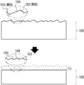
- laser processing includes a strain layer 101 into which processing damages such as scratches 1011 and latent scratches 1012 and strains 1013 have been introduced. It has a bulk layer 102 in which such processing damage is not introduced (see FIG. 8).
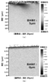
- this strain layer 101 can be confirmed by the SEM-EBSD method, TEM, ⁇ XRD, Raman spectroscopy, or the like. In order to grow a high-quality SiC ingot, it is preferable to remove the strain layer 101 to expose the bulk layer 102 to which no processing damage has been introduced.
- a step-terrace structure is confirmed on the surface of the SiC single crystal 10 flattened at the atomic level.
- This step-terrace structure is a staircase structure in which step 103, which is a stepped portion having one or more molecular layers, and terrace 104, which is a flat portion where the ⁇ 0001 ⁇ surface is exposed, are alternately arranged (FIG. 10 and FIG. See FIG. 12).
- step 103 one molecular layer (0.25 nm) is the minimum height (minimum unit), and various step heights are formed by overlapping a plurality of the single molecular layers.
- MSB the one in which step 103 is bundled (bunched) to become huge and has a height exceeding one unit cell of each polytype.
- the MSB refers to step 103 that bunched beyond the 4 molecular layer (5 or more molecular layers). Further, in the case of 6H-SiC, it refers to step 103 bunching beyond the 6-layer (7-layer or more).
- the heat treatment step S1 is a step of heat-treating the SiC single crystal 10 in an atmosphere containing Si element and C element.
- the SiC seed crystal 11 that has undergone the heat treatment step S1 has a surface in which at least one or more of strain (strain layer 101), BPD, and MSB is reduced. Therefore, in the ingot growth step S2, which is a later step, it is possible to prevent the SiC ingot 12 from inheriting the distortion caused by the strain of the SiC seed crystal 11, the BPD, and the MSB. That is, it is possible to manufacture a high quality SiC ingot 12.
- the heat treatment step S1 is an etching step of transporting the SiC element and the C element from the SiC single crystal body 10 to the SiC material to etch the SiC single crystal body 10, and conversely, the SiC single crystal body from the SiC material.
- a crystal growth step of transporting the Si element and the C element to the 10 to grow the SiC single crystal 10 into a crystal may be included.
- the specific embodiment of the heat treatment step S1 is not particularly limited as long as it is a step capable of removing or reducing the strain layer 101, BPD and MSB contained in the SiC single crystal body 10.
- the temperature gradient and the chemical potential difference between the SiC single crystal body 10 and the SiC material can be adopted.
- the SiC material is composed of SiC that can receive or transfer Si element and C element to and from the SiC single crystal body 10 by heating it relative to the SiC single crystal body 10.
- a container made of SiC (main body container 20) or a substrate made of SiC (SiC member) can be adopted.
- the crystal polymorph of this SiC material any polymorphic type can be adopted, and polycrystalline SiC may be adopted.
- the SiC single crystal 10 and the SiC material are preferably placed in a semi-closed space and heated.
- the surface of the SiC single crystal 10 was etched and grown, and at least one or more of the strain layers 101, BPD and MSB was reduced.
- a surface can be formed.
- the term "quasi-closed space” as used herein refers to a space in which the inside of the container can be evacuated, but at least a part of the vapor generated in the container can be confined.
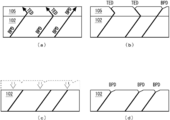
- a preferred embodiment of the heat treatment step S1 can be roughly divided into an etching step of etching the surface of the SiC single crystal body 10 and a crystal growth step of growing a single crystal SiC crystal on the SiC single crystal body 10 (FIG. 6). 2).
- FIG. 3 is an explanatory diagram showing an outline of the etching process.
- the SiC single crystal 10 is placed in a semi-closed space where the SiC material is exposed and heated in a temperature range of 1400 ° C. or higher and 2300 ° C. or lower, so that the reactions 1) to 5) below are sustained. It is considered that the etching proceeds as a result.
- the Si atom sublimation step of thermally sublimating the Si atom from the surface of the SiC single crystal body 10 and the C atom remaining on the surface of the SiC single crystal body 10 and the Si vapor in the semi-closed space are combined. It includes a C atom sublimation step of sublimating from the surface of the SiC single crystal body 10 by reacting.
- the etching step heats the SiC single crystal 10 on the high temperature side of the temperature gradient and the SiC material on the low temperature side of the temperature gradient.
- an etching space X is formed between the SiC single crystal 10 and the SiC material, and the surface of the SiC single crystal 10 can be etched using the temperature gradient as a driving force.
- Crystal growth process According to the crystal growth step (step located on the right side of FIG. 2), the BPD existing on the surface of the SiC single crystal 10 is converted into another dislocation, and the BPD exposed on the surface of the SiC seed crystal 11 is removed or reduced. be able to. Further, the MSB on the surface of the SiC seed crystal 11 can be removed or reduced.
- FIG. 4 is an explanatory diagram showing an outline of the crystal growth process.
- the reaction of 1) to 5) below is sustained by arranging the SiC single crystal 10 in a semi-closed space where the SiC material is exposed and heating in a temperature range of 1400 ° C. or higher and 2300 ° C. or lower. It is considered that the crystal growth progresses as a result.
- the crystal growth step sublimates the C atoms remaining on the surface of the SiC material by reacting the Si atom sublimation step of thermally sublimating the Si atoms from the surface of the SiC material with the Si vapor in the semi-closed space.
- the raw material is transferred to the C atom sublimation step, the raw material transporting step of transporting the raw materials (Si atom and C atom) to the surface of the SiC single crystal 10 using the temperature gradient and the chemical potential difference as the driving force, and the step of the SiC single crystal 10.
- the SiC material is heated on the high temperature side of the temperature gradient, and the SiC single crystal 10 is heated on the low temperature side of the temperature gradient.
- the raw material supply space Y is formed between the SiC single crystal 10 and the SiC material, and the SiC single crystal 10 can be crystal-grown by using the temperature gradient as a driving force.
- the partial pressure difference (chemical potential difference) generated on the surfaces of the polycrystalline SiC and the single crystal SiC is transported as a raw material. Crystals can be grown as a driving force for. In this case, a temperature gradient may or may not be provided.
- the heat treatment step S1 has been roughly divided into an etching step and a crystal growth step.
- the heat treatment step S1 can be classified into two types from the viewpoint of the environment for heating the SiC single crystal body 10.
- the SiC single crystal 10 is heated in a SiC-Si equilibrium vapor pressure environment and in a SiC-C equilibrium vapor pressure environment. It can be classified into the form to be used and the form to be used.
- the SiC-Si equilibrium vapor pressure environment refers to a vapor pressure environment when SiC (solid) and Si (liquid phase) are in a phase equilibrium state via a gas phase.
- the SiC-C equilibrium vapor pressure environment refers to a vapor pressure environment when SiC (solid phase) and C (solid phase) are in a phase equilibrium state via a gas phase.
- the SiC-Si equilibrium vapor pressure environment and the SiC-C equilibrium vapor pressure environment in the present specification include a near thermal equilibrium vapor pressure environment that satisfies the relationship between the growth rate and the growth temperature derived from the theoretical thermal equilibrium environment.
- the atomic number ratio Si / C in the gas phase of the SiC-Si equilibrium vapor pressure environment is larger than the atomic number ratio Si / C in the gas phase of the SiC-C equilibrium vapor pressure environment.
- the SiC-Si equilibrium vapor pressure environment can be formed by arranging the SiC single crystal 10 in a semi-closed space having an atomic number ratio of Si / C exceeding 1 and heating it.
- a SiC container main body container 20
- SiC single crystal 10 having a chemical ratio of 1: 1 and a SiC material having a chemical ratio of 1: 1.
- the Si steam supply source Si pellets or the like
- the atomic number ratio Si / C in the semi-closed space exceeds 1.
- the SiC-C equilibrium vapor pressure environment can be formed by arranging the SiC single crystal 10 in a semi-closed space having an atomic number ratio of Si / C of 1 or less and heating it.
- a SiC container main body container 20
- a SiC single crystal 10 having a chemical ratio of 1: 1 and a SiC material having a chemical ratio of 1: 1.
- the atomic number ratio Si / C in the main body container 20 becomes 1.
- a C steam supply source (C pellet or the like) may be arranged to set the atomic number ratio Si / C to 1 or less.
- the heat treatment step S1 is (1) an etching step or a crystal growth step, (2) heat treatment under a SiC-Si equilibrium vapor pressure environment, or a SiC-C equilibrium vapor pressure environment. It can be classified from the viewpoint of whether to perform heat treatment below. By associating this combination of classifications with effects, it can be classified into the following four types.
- the strain layer 101 of the SiC single crystal 10 can be removed by etching, and MSB is formed on the surface after etching. Therefore, it is classified as the etching bunching step S111 (lower left of FIG. 2).
- the strain layer 101 of the SiC single crystal 10 can be removed by etching, and MSB is not formed on the surface after etching. Therefore, it is classified as the etching flattening step S121 (upper left of FIG. 2).
- the crystal growth step is performed in a SiC-Si equilibrium vapor pressure environment, it is possible to form a growth layer 105 on which the MSB is reduced or removed on the SiC single crystal body 10. Therefore, it is classified as the growth flattening step S122 (upper right of FIG. 2).
- the MSB can be removed or reduced in the etching flattening step S121 and the growth flattening step S122, they are collectively classified as the flattening step S12 (upper side of FIG. 2).
- the crystal growth step is performed in a SiC-C equilibrium vapor pressure environment, it is possible to remove or reduce BPD in the growth layer 105. Therefore, it is classified as the basal plane dislocation reduction step S13 (lower right of FIG. 2).
- the main body container 20 preferably has a structure in which the SiC material is exposed in the internal space.
- the entire main body container 20 is made of a SiC material (polycrystalline SiC). By heating the main body container 20 made of such a material, an atmosphere containing Si element and C element can be generated inside (semi-closed space).
- the environment inside the heat-treated main body container 20 be a vapor pressure environment of a mixed system of a gas phase species containing a Si element and a gas phase species containing a C element.
- the gas phase species containing the Si element include Si, Si 2 , Si 3 , Si 2 C, SiC 2 , and SiC.
- the gas phase species containing the C element include Si 2 C, SiC 2 , SiC and C. That is, the SiC gas is present in the main container 20.
- this configuration can be adopted as long as the vapor pressure of the vapor phase species containing the Si element and the vapor pressure species containing the C element is generated in the internal space during the heat treatment of the main container 20.
- a configuration in which the SiC material is exposed on a part of the inner surface or a configuration in which the SiC material (such as a SiC substrate) is separately arranged in the main body container 20 can be shown.
- the SiC single crystal 10 is housed inside the main body container 20 and the main body container 20 is heated so that a temperature gradient is formed inside.
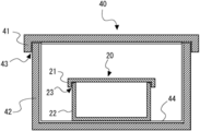
- the apparatus configuration main container 20, heating furnace 30, high melting point container 40
- the main body container 20 is a fitting container including an upper container 21 and a lower container 22 that can be fitted to each other.
- a minute gap 23 is formed in the fitting portion between the upper container 21 and the lower container 22, and the inside of the main container 20 can be exhausted (evacuated) from the gap 23. That is, the inside of the main body container 20 is a semi-closed space.
- the heating furnace 30 has a configuration in which the main body container 20 can be heated by providing a temperature gradient in an atmosphere containing Si element.
- the heating furnace 30 includes a main heating chamber 31 capable of heating an object to be treated (SiC single crystal 10 or the like) to a temperature of 1000 ° C. or higher and 2300 ° C. or lower.
- a preheating chamber 32 capable of preheating the object to be processed to a temperature of 500 ° C. or higher
- a melting point container 40 capable of accommodating the main body container 20, and the melting point container 40 are moved from the preheating chamber 32 to the main heating chamber 31. It is provided with a possible moving means 33 (moving table).
- the heating chamber 31 is formed in a regular hexagonal shape in a plan sectional view, and the melting point container 40 is arranged inside the heating chamber 31.
- a heating heater 34 (mesh heater) is provided inside the heating chamber 31.
- a multilayer heat-reflecting metal plate is fixed to the side wall or ceiling of the heating chamber 31 (not shown). The multilayer heat-reflecting metal plate is configured to reflect the heat of the heating heater 34 toward the substantially central portion of the main heating chamber 31.
- the heating heater 34 is arranged so as to surround the melting point container 40 in which the object to be processed is housed, and further, the multilayer heat-reflecting metal plate is arranged outside the heating heater 34, whereby 1000 ° C.
- the temperature can be raised to 2300 ° C. or lower.
- a resistance heating type heater or a high frequency induction heating type heater can be used as the heating heater 34.
- the heating heater 34 may adopt a configuration capable of forming a temperature gradient in the melting point container 40.
- the heating heater 34 may be configured so that many heaters are arranged on the upper side (or lower side). Further, the heating heater 34 may be configured so that the width increases toward the upper side (or the lower side). Alternatively, the heating heater 34 may be configured so that the electric power supplied can be increased toward the upper side (or the lower side).
- a vacuum forming valve 35 for exhausting the inside of the main heating chamber 31, an inert gas injection valve 36 for introducing an inert gas into the main heating chamber 31, and the main heating chamber 31
- a vacuum gauge 37 for measuring the degree of vacuum inside is connected.
- the vacuum forming valve 35 is connected to a vacuum drawing pump that exhausts the inside of the main heating chamber 31 to create a vacuum (not shown). With the vacuum forming valve 35 and the vacuum pulling pump, the degree of vacuum in the heating chamber 31 can be adjusted to, for example, 10 Pa or less, more preferably 1 Pa or less, still more preferably 10 -3 Pa or less. As this evacuation pump, a turbo molecular pump can be exemplified.
- the Inert gas injection valve 36 is connected to the Inactive gas supply source (not shown). With the inert gas injection valve 36 and the inert gas supply source, the inert gas can be introduced into the heating chamber 31 in the range of 10-5 to 10000 Pa. As the inert gas, Ar, He, N 2, or the like can be selected.
- the preheating chamber 32 is connected to the main heating chamber 31, and is configured so that the melting point container 40 can be moved by the moving means 33.
- the preheating chamber 32 of the present embodiment is configured so that the temperature can be raised by the residual heat of the heating heater 34 of the main heating chamber 31. For example, when the temperature of the main heating chamber 31 is raised to 2000 ° C., the temperature of the preheating chamber 32 is raised to about 1000 ° C., and the object to be treated (SiC single crystal 10, main body container 20, high melting point container 40, etc.) Can be degassed.
- the moving means 33 is configured to be movable between the main heating chamber 31 and the preheating chamber 32 on which the melting point container 40 is placed. Since the transfer between the main heating chamber 31 and the preheating chamber 32 by the moving means 33 is completed in about 1 minute at the shortest, the temperature can be raised or lowered at 1 to 1000 ° C./min. In this way, since the manufacturing apparatus can rapidly raise the temperature and lower the temperature, it is possible to observe a surface shape that does not have a history of low-temperature growth during raising and lowering, which was difficult with the conventional apparatus. is there. Further, in FIG. 6, the preheating chamber 32 is arranged below the main heating chamber 31, but the present invention is not limited to this, and the preheating chamber 32 may be arranged in any direction.
- the moving means 33 is a moving table on which the high melting point container 40 is placed. A small amount of heat is released from the contact portion between the moving table and the melting point container 40. As a result, a temperature gradient can be formed in the high melting point container 40.
- a temperature gradient is provided so that the temperature decreases from the upper container 41 to the lower container 42 of the melting point container 40. ..
- the direction of this temperature gradient can be set to any direction by changing the position of the contact portion between the moving table and the melting point container 40.
- the temperature gradient is provided so that the temperature rises from the upper container 41 of the high melting point container 40 toward the lower container 42. It is desirable that this temperature gradient is formed along the front and back directions of the SiC single crystal body 10. Further, as described above, a temperature gradient may be formed depending on the configuration of the heating heater 34.
- the atmosphere containing the Si element in the heating furnace 30 is formed by using the high melting point container 40 and the Si steam supply source 44.
- any method capable of forming an atmosphere containing a Si element around the main body container 20 can be adopted in the apparatus for producing the SiC seed crystal 11.
- the melting point container 40 is configured to include a melting point material.
- a general purpose heat-resistant member C, W is a refractory metal, Re, Os, Ta, Mo , Ta 9 C 8 is a carbide, HfC, TaC, NbC, ZrC , Ta 2 C, TiC, WC, MoC, a nitride HfN, TaN, BN, Ta 2 N, ZrN, TiN, HfB 2, TaB 2, ZrB 2, NB 2, TiB 2 is a boride, it can be exemplified polycrystalline SiC.
- the high melting point container 40 is a fitting container including an upper container 41 and a lower container 42 that can be fitted to each other, and is configured to be able to accommodate the main body container 20.
- a minute gap 43 is formed in the fitting portion between the upper container 41 and the lower container 42, and the inside of the high melting point container 40 can be exhausted (evacuated) from the gap 43. That is, like the main container 20, the inside of the melting point container 40 is preferably a semi-closed space.
- the high melting point container 40 has a Si steam supply source 44 capable of supplying Si steam in the high melting point container 40.
- the Si steam supply source 44 may be configured to generate Si steam in the melting point container 40 during heat treatment.
- Examples of the Si vapor supply source 44 include solid Si (Si pellets such as single crystal Si pieces and Si powder) and Si compounds.
- TaC is adopted as the material of the melting point container 40
- tantalum silicide is adopted as the Si vapor supply source 44. That is, as shown in FIG. 5, a tantalum silicide layer is formed inside the melting point container 40, and Si vapor is supplied from the tantalum silicide layer into the container during the heat treatment. As a result, a Si vapor pressure environment is formed in the high melting point container 40, and the main body container 20 can be heated in an atmosphere containing Si elements. In addition to this, any configuration can be adopted as long as an atmosphere containing Si element is formed in the melting point container 40 during the heat treatment.
- the main body container 20 contains the Si element from the inside of the main body container 20 by heating in an atmosphere containing the Si element (for example, a Si vapor pressure environment). It is possible to suppress the exhaust of vapor phase species. That is, the environment inside the main body container 20 is maintained by balancing the vapor pressure of the vapor phase species containing the Si element inside the main body container 20 and the vapor pressure of the gas phase species containing the Si element outside the main body container 20. be able to.
- an atmosphere containing the Si element for example, a Si vapor pressure environment.
- the main body container 20 is composed of polycrystalline SiC. With such a configuration, when the main body container 20 is heated by using the heating furnace 30, steam of a gas phase type containing Si element and a gas phase type containing C element is generated in the main body container 20. Can be done.
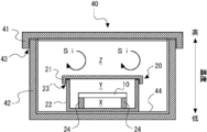
- the outline of the device configuration for realizing the etching process is shown on the left side of FIG. 7.
- the SiC single crystal 10 is located on the high temperature side of the temperature gradient, and the SiC material (a part of the main body container 20) is located on the low temperature side of the temperature gradient.
- It has a space X. That is, the etching space X is formed by arranging the SiC single crystal 10 at a position where the temperature is higher than that of the SiC material (for example, the bottom surface of the lower container 22) due to the temperature gradient formed by the heating furnace 30. There is.
- the etching space X is a space for transporting Si atoms and C atoms on the surface of the SiC single crystal body 10 to the main body container 20 by using a temperature difference provided between the SiC single crystal body 10 and the main body container 20 as a driving force. For example, when the temperature on the surface of the SiC single crystal 10 and the temperature on the bottom surface of the lower container 22 facing the surface are compared, the temperature on the surface side of the SiC single crystal 10 is higher, and the temperature on the bottom surface side of the lower container 22 is higher. The main body container 20 is heated so that the temperature becomes low (see the left side of FIG. 7).
- etching space X a space having a temperature difference between the surface of the SiC single crystal 10 and the bottom surface of the lower container 22
- Si atoms and C atoms are transported using the temperature difference as a driving force.
- the surface of the SiC single crystal 10 can be etched (the white arrow on the right side of FIG. 7 is the direction of transportation).
- the main body container 20 may have a substrate holder 24 provided between the SiC single crystal body 10 and the main body container 20.
- the heating furnace 30 has a structure capable of heating by forming a temperature gradient such that the temperature decreases from the upper container 21 to the lower container 22 of the main container 20. Therefore, a substrate holder 24 capable of holding the SiC single crystal 10 is provided between the SiC single crystal 10 and the lower container 22, and an etching space X is formed between the SiC single crystal 10 and the lower container 22. You may.
- the substrate holder 24 may have a structure capable of holding at least a part of the SiC single crystal body 10 in the hollow of the main body container 20.
- any conventional support means such as one-point support, three-point support, a configuration for supporting the outer peripheral edge, or a configuration for sandwiching a part thereof can be naturally adopted.
- the substrate holder 24 may not be provided depending on the direction of the temperature gradient of the heating furnace 30.
- the heating furnace 30 forms a temperature gradient so that the temperature decreases from the lower container 22 toward the upper container 21
- a SiC single crystal is formed on the bottom surface of the lower container 22 (without providing the substrate holder 24). 10 may be arranged.
- the SiC single crystal 10 is located on the low temperature side of the temperature gradient, and the SiC material (a part of the main body container 20) is located on the high temperature side of the temperature gradient. It has a raw material supply space Y. That is, the raw material supply space Y is formed by arranging the SiC single crystal 10 at a position lower than the SiC material (for example, the top surface of the upper container 21) due to the temperature gradient formed by the heating furnace 30. Has been done.
- the raw material supply space Y in addition to the SiC single crystal body 10, there are a Si atom supply source and a C atom supply source as raw materials. Then, by heating these, Si atoms and C atoms which are the raw materials of the SiC single crystal 10 are supplied into the raw material supply space Y. The Si atoms and C atoms are transported to the surface of the SiC single crystal body 10 and recrystallized to form a growth layer 105 (the black arrow on the right side of FIG. 7 indicates the direction of transport).
- the main body container 20 is formed of polycrystalline SiC (Poly-SiC), so that the main body container 20 itself is used as a Si atom supply source and a C atom supply source.
- Si atom supply source and the C atom supply source a material capable of supplying Si atoms such as a Si substrate, a material capable of supplying C atoms such as graphite, and Si atoms and C atoms such as a SiC substrate can be supplied.
- the material can be adopted.
- the arrangement of the Si atom supply source and the C atom supply source is not limited to this form, and any form may be used as long as the Si atom and the C atom can be supplied into the raw material supply space Y.
- the vapor pressure difference (chemical potential difference) between the polycrystalline SiC (raw material) and the single crystal SiC (SiC single crystal body 10) can be used as the growth driving force.
- a temperature gradient is provided so that the temperature decreases toward the SiC single crystal body 10.
- the transport of Si atoms and C atoms to the SiC single crystal 10 occurs, so that the growth rate of the growth layer 105 increases (the black arrow on the right side of FIG. 7 indicates the direction of transport). ..
- the Si atom supply source and the C atom supply source may be brought close to the SiC single crystal body 10.
- the Si atom supply source and the polycrystalline SiC upper container 21 serving as the C atom supply source can be arranged in parallel with the SiC single crystal body 10.
- the distance between the surface of the SiC single crystal 10 and the top surface of the upper container 21 is preferably set to 100 mm or less, more preferably 10 mm or less, still more preferably 2.7 mm or less. Further, it is preferably set to 0.7 mm or more, more preferably 1.2 mm or more, and further preferably 1.7 mm or more.
- the etching space X and the raw material supply space Y are exhausted (evacuated) through the Si vapor pressure space Z. That is, the main body container 20 having the etching space X and / or the raw material supply space Y is arranged in the melting point container 40 having the Si vapor pressure space Z, and the SiC single crystal 10 is further arranged in the main body container 20. Is desirable.
- the SiC-Si equilibrium vapor pressure environment can be formed by arranging the SiC single crystal 10 in a semi-closed space having an atomic number ratio of more than 1 and heating it.
- the SiC single crystal body 10 satisfying the chemical quantity theory ratio 1: 1 and the chemical quantity are contained in the main body container 20 of polycrystalline SiC satisfying the chemical quantity theory ratio 1: 1.
- the atomic number ratio Si / C in the main body container 20 is 1. It will exceed.
- the inside of the main body container 20 approaches a SiC-Si equilibrium vapor pressure environment.
- the outline of the device configuration for realizing the SiC-C equilibrium vapor pressure environment is shown on the lower side of FIG. 7.
- the SiC-C equilibrium vapor pressure environment can be formed by arranging the SiC single crystal 10 in a semi-closed space having an atomic number ratio of 1 or less and heating it.
- a SiC single crystal body 10 satisfying the chemical quantity theory ratio 1: 1 and a chemical quantity are contained in the main body container 20 of the polycrystalline SiC satisfying the chemical quantity theory ratio 1: 1.
- the SiC substrate holder 24 satisfying the ratio of 1: 1 is arranged, the number of atoms ratio Si / C in the main body container 20 is 1 or 1 or less.
- the inside of the main body container 20 approaches the SiC-C equilibrium vapor pressure environment.
- the C steam supply source may be separately arranged, or the main body container 20 including the C steam supply source and the substrate holder 24 may be adopted. ..
- the C steam supply source include solid C (C pellets such as C substrate and C powder) and C compounds.
- the SiC seed crystal 11 from which the strain layer 101 of the SiC single crystal 10 has been removed can be obtained. Further, if the heat treatment step S1 for growing crystals in a SiC-C equilibrium vapor pressure environment is performed, a high-quality SiC seed crystal 11 having a growth layer 105 from which BPD has been removed or reduced can be obtained.
- the heat treatment step S1 for etching or crystal growth is performed in a SiC-Si equilibrium vapor pressure environment, the surface of the SiC single crystal 10 can be flattened. That is, it is possible to obtain a SiC seed crystal 11 in which the MSB is removed or reduced. As a result, it is possible to prevent defects caused by the MSB or the like from being inherited by the SiC ingot by the ingot growth step S2, which is a later step.
- the strain layer removing step S11 is a step of removing the strain layer 101 introduced into the SiC single crystal body 10.
- the strain layer removing step S11 will be described, but the description will be omitted if it overlaps with the general description of the heat treatment step S1 described above.
- the SiC single crystal body 10 and the SiC material are placed in a semi-closed space having an atomic number ratio of Si / C of 1 or less. Is a step of heating the SiC single crystal body 10 so as to be on the high temperature side and the SiC material on the low temperature side (etching bunching step S111).
- the SiC single crystal body 10 and the SiC material are arranged so as to face each other in a semi-closed space in which the atomic number ratio Si / C exceeds 1.
- the step of heating the SiC single crystal 10 to the high temperature side and the SiC material to the low temperature side (etching flattening step S121).
- the SiC single crystal 10 and the SiC material are arranged so as to face each other, and the SiC single crystal 10 is on the high temperature side and the SiC material is placed in a SiC-Si equilibrium vapor pressure environment or a SiC-C equilibrium vapor pressure environment. Is a step of heating so that is on the low temperature side.
- the SiC single crystal 10 arranged on the high temperature side of the temperature gradient and a part of the main body container 20 arranged on the low temperature side of the temperature gradient are heat-treated so as to face each other. Atoms are transported from 10 to the main body container 20 to achieve etching of the SiC single crystal body 10.
- the surface of the SiC single crystal 10 and the bottom surface of the main body container 20 having a temperature lower than this surface are arranged so as to face each other, so that an etching space X is formed between them.
- this etching space X atoms are transported by using the temperature gradient formed by the heating furnace 30 as a driving force, and as a result, the SiC single crystal 10 can be etched.
- the back surface of the SiC single crystal body 10 and the top surface of the main body container 20 having a temperature higher than this back surface are arranged relative to each other.
- a raw material supply space Y may be formed between them.
- the raw material is transported by using the temperature gradient formed by the heating furnace 30 as a driving force, and as a result, the growth layer 105 can be formed on the back surface side of the SiC single crystal body 10.
- the strain layer removing step S11 a configuration may be adopted in which the raw material supply space Y is not formed by bringing the back surface side of the SiC single crystal body 10 into contact with the top surface of the main body container 20.
- the main body container 20 is arranged in the Si vapor pressure space Z in which an atmosphere containing a Si element is formed.
- the main body container 20 is arranged in the Si vapor pressure space Z, and the inside of the main body container 20 is exhausted (evacuated) through the space of the Si vapor pressure environment, so that Si atoms are discharged from the inside of the main body container 20. It can be suppressed from decreasing. As a result, the preferable atomic number ratio Si / C in the main body container can be maintained for a long time.
- the etching temperature in the strain layer removing step S11 is preferably set in the range of 1400 to 2300 ° C, and more preferably set in the range of 1600 to 2000 ° C.
- the etching rate in the strain layer removing step S11 can be controlled by the above temperature range, and can be selected in the range of 0.001 to 2 ⁇ m / min.
- the etching amount in the strain layer removing step S11 can be adopted as long as it is an etching amount capable of removing the strain layer 101 of the SiC single crystal body 10. As the etching amount, 0.1 ⁇ m or more and 20 ⁇ m or less can be exemplified, but it can be applied as needed.
- the etching time in the strain layer removing step S11 can be set to an arbitrary time so as to obtain a desired etching amount. For example, when the etching rate is 1 ⁇ m / min and the etching amount is desired to be 1 ⁇ m, the etching time is 1 minute.
- the temperature gradient in the strain layer removing step S11 is set in the range of 0.1 to 5 ° C./mm in the etching space X.
- the SiC seed crystal 11 in which the strain layer 101 is removed or reduced can be produced.
- the flattening step S12 is a step of decomposing and removing the MSB formed on the surface of the SiC seed crystal 11 as shown in FIGS. 10 and 12.
- the etching flattening step S121 and the growth flattening step S122 are preferably exemplified in the flattening step S12.
- the flattening step S12 will be described, but the description will be omitted if it overlaps with the general description of the heat treatment step S1 described above.
- the etching flattening step S121 is a step of reducing or removing the MSB by etching the surface of the SiC single crystal 10 on which the MSB is formed.
- the SiC single crystal body 10 and the SiC material are placed in a semi-closed space having an atomic number ratio of Si / C of more than 1.
- This is a step in which the SiC single crystals 10 are arranged so as to face each other and heated so that the SiC single crystal 10 is on the high temperature side and the SiC material is on the low temperature side.
- the apparatus configuration for realizing the etching flattening step S121 is such that the Si vapor supply source 25 is further arranged in the main body container 20 of the strain layer removing step S11.
- the Si steam supply source 25 By arranging the Si steam supply source 25, the SiC single crystal 10 can be heated in a SiC-Si equilibrium vapor pressure environment.
- the description of the portion overlapping with the general description of the strain layer removing step S11 will be omitted as appropriate.
- the etching temperature in the etching flattening step S121 is preferably set in the range of 1400 to 2300 ° C, more preferably in the range of 1600 to 2000 ° C.
- the etching rate in the etching flattening step S121 can be controlled by the above temperature range, and can be selected in the range of 0.001 to 2 ⁇ m / min.
- the etching amount in the etching flattening step S121 can be adopted as long as it is an etching amount capable of decomposing the MSB of the SiC single crystal body 10. As the etching amount, 0.1 ⁇ m or more and 20 ⁇ m or less can be exemplified.
- the etching time in the etching flattening step S121 can be set to an arbitrary time so as to obtain a desired etching amount. For example, when the etching rate is 1 ⁇ m / min and the etching amount is desired to be 1 ⁇ m, the etching time is 1 minute.
- the temperature gradient in the etching flattening step S121 is set in the range of 0.1 to 5 ° C./mm in the etching space X.
- the etching flattening step S121 by etching the surface of the SiC single crystal body 10, it is possible to produce the SiC seed crystal 11 in which the MSB is removed or reduced.
- the growth flattening step S122 is a step of forming a growth layer 105 in which the MSB is reduced or removed by growing crystals on the surface of the SiC single crystal 10 on which the MSB is formed.
- the SiC single crystal 10 and the SiC material are placed in a semi-closed space having an atomic number ratio of Si / C of more than 1.
- This is a step in which the SiC single crystals 10 are arranged so as to face each other and heated so that the SiC single crystal 10 is on the low temperature side and the SiC material is on the high temperature side.
- the surface of the SiC single crystal 10 and the top surface of the main body container 20 having a temperature higher than this surface are arranged so as to face each other, so that the raw material supply space Y is formed between them.
- the raw material is transported by the temperature gradient formed by the heating furnace 30 and the chemical potential difference between the SiC single crystal 10 and the SiC material as a driving force, and as a result, the surface of the SiC single crystal 10 is transported.
- the growth layer 105 can be formed.
- the apparatus configuration for realizing the growth flattening step S122 is a configuration in which the Si vapor supply source 25 is further arranged in the main body container 20 as in the etching flattening step S121.
- the description of the parts that overlap with the general description of the etching flattening step S121 described above will be omitted.
- the heating temperature in the growth flattening step S122 is preferably set in the range of 1400 to 2200 ° C, more preferably in the range of 1600 to 2000 ° C.
- the growth rate in the growth flattening step S122 can be controlled by the above temperature range and can be selected in the range of 0.001 to 1 ⁇ m / min.
- the amount of growth in the growth flattening step S122 is preferably 5 ⁇ m or more, and more preferably 8 ⁇ m or more.
- the growth time in the growth flattening step S122 can be set to an arbitrary time so as to achieve a desired growth amount. For example, when the growth rate is 10 nm / min and the amount of growth is desired to be 10 ⁇ m, the growth time is 100 minutes.
- the degree of vacuum (main heating chamber 31) in the growth flattening step S122 is 10-5 to 10 Pa, more preferably 10 -3 to 1 Pa.
- an inert gas during growth. Ar or the like can be selected as the inert gas, and the degree of vacuum of the heating furnace 30 (main heating chamber 31) can be adjusted by introducing the inert gas in the range of 10-5 to 10000 Pa. it can.
- the SiC seed crystal 11 in which the MSB is removed or reduced is produced by growing the growth layer 105 having no MSB on the surface of the SiC single crystal 10. can do.
- the basal dislocation reduction step S13 is a step of forming a growth layer 105 in which BPD is removed or reduced by growing crystals under the condition that the terrace width W of the SiC single crystal 10 is increased. is there.
- the description of the parts that overlap with the general description of the heat treatment step S1 described above will be omitted.
- the SiC single crystal body 10 and the SiC material are contained in a semi-closed space having an atomic number ratio of Si / C of 1 or less.
- This is a step of heating the SiC single crystal body 10 so as to be on the low temperature side and the SiC material on the high temperature side.
- the apparatus configuration for realizing the basal dislocation reduction step S13 is the SiC single crystal 10 arranged on the low temperature side of the temperature gradient and the SiC single crystal 10 arranged on the high temperature side of the temperature gradient.
- the raw material is transported from the main body container 20 to the SiC single crystal body 10 to form the growth layer 105.
- the Si vapor supply source 25 is not arranged. It should be noted that the description of the parts that overlap with the general description of the growth flattening step S122 described above will be omitted.
- the heating temperature in the basal dislocation reduction step S13 is preferably set in the range of 1400 to 2200 ° C, more preferably in the range of 1600 to 2000 ° C.
- the growth rate in the basal dislocation reduction step S13 can be controlled by the above temperature region and the growth environment, and can be selected in the range of 0.001 to 1 ⁇ m / min.
- the amount of growth in the basal dislocation reduction step S13 is preferably 5 ⁇ m or more, and more preferably 8 ⁇ m or more.
- the growth time in the basal dislocation reduction step S13 can be set to an arbitrary time so as to achieve a desired growth amount. For example, when the growth rate is 10 nm / min and the amount of growth is desired to be 10 ⁇ m, the growth time is 100 minutes.
- the degree of vacuum (main heating chamber 31) in the basal dislocation reduction step S13 is 10-5 to 10 Pa, more preferably 10 -3 to 1 Pa.
- an inert gas during growth. Ar or the like can be selected as the inert gas, and the degree of vacuum of the heating furnace 30 (main heating chamber 31) can be adjusted by introducing the inert gas in the range of 10-5 to 10000 Pa. it can.
- the conversion rate (BPD conversion rate) at which BPD is converted into other defects / dislocations is improved by growing the terrace 104 under the condition of increasing the width (terrace width W).
- the BPD density in the growth layer 105 can be reduced or removed.
- the condition for increasing the terrace width W is a condition for increasing the terrace width W2 after growth as compared with the terrace width W1 before growth, for example, growing in a SiC-C equilibrium vapor pressure environment or a C-rich environment. It can be realized by.
- the basal plane dislocation reduction step S13 is performed after the flattening step S12. That is, when comparing the width of the terrace 104 on the surface on which the MSB is not formed and the width of the terrace 104 on the surface on which the MSB is formed, the terrace 104 on the surface on which the MSB is not formed is wider than the terrace 104. Is narrow. Therefore, the BPD conversion rate can be improved by growing the growth layer 105 under the condition that the MSB is formed after the decomposition of the MSB.
- FIG. 16A shows a mode in which the strain layer removing step S11 is performed as the heat treatment step S1 and the SiC seed crystal 11 thus obtained is subjected to the ingot growth step S2.
- the SiC seed crystal 11 from which the strain layer 101 has been removed can be obtained. That is, it is possible to prevent the defects caused by the strain layer 101 from being inherited by the SiC ingot 12.
- either the etching bunching step S111 or the etching flattening step S121 can be adopted.
- the strain layer 101 can be removed and the MSB can be removed or reduced at the same time.
- FIG. 16B shows a mode in which the flattening step S12 is performed after the strain layer removing step S11. According to such a form, the SiC seed crystal 11 having no strain layer 101 and MSB on its surface can be produced. This makes it possible to manufacture a high quality SiC ingot 12.
- FIG. 16C shows a mode in which the basal plane dislocation reduction step S13 is performed after the strain layer removing step S11 and the flattening step S12.
- FIG. 16D is a form in which the flattening step S12 is further performed after the basal plane dislocation reduction step S13 in the form shown in FIG. 16C.
- any of the etching flattening step S121 and the growth flattening step S122 can be adopted.
- the heat treatment step S1 is selected from a strain layer removing step S11 (etching bunching step S111 or etching flattening step S121), a flattening step S12 (etching flattening step S121 or growth flattening step S122), and a basal plane rearrangement reduction step S13.
- a strain layer removing step S11 etching bunching step S111 or etching flattening step S121
- a flattening step S12 etching flattening step S121 or growth flattening step S122
- a basal plane rearrangement reduction step S13 When the form includes two or more types, the two or more types of steps can be heat-treated with the same apparatus configuration.
- Examples of the container in which the plurality of heat treatment steps S1 are performed include a container that generates an atmosphere of Si element and C element in the internal space, specifically, a main body container 20. As described above, by using the main body container 20 and the like, even if the heat treatment step S1 includes a plurality of steps, all of them can be completed in the same container, so that the work can be expected to be simplified. Further, since etching and crystal growth can be performed in the same device system, it is not necessary to introduce a plurality of devices, which is very advantageous in industry.
- the present invention also relates to a SiC seed crystal 11 produced through the heat treatment step S1.
- the surface of the SiC seed crystal 11 of the present invention does not contain factors such as strain layer 101, BPD, and MSB that adversely affect ingot growth in the heat treatment step S1. Therefore, according to the SiC seed crystal 11 of the present invention, it is possible to grow a higher quality SiC ingot.
- the SiC seed crystal 11 is preferably characterized by having a growth layer 105 on its surface that does not contain BPD.
- the thickness of the growth layer 105 containing no BPD is preferably 0.001 ⁇ m or more, more preferably 0.01 ⁇ m or more, and further preferably 0.1 ⁇ m or more. When the thickness of the layer containing no BPD is within the above range, it is possible to suppress the propagation of BPD present in the SiC seed crystal 11 to the ingot in the growth step of growing SiC on the SiC seed crystal 11. ..
- the diameter of the SiC seed crystal 11 of the present invention is not particularly limited, and is preferably 6 inches or more, more preferably 8 inches or more, and further preferably 12 inches or more.
- the ingot growth step S2 is a step of growing a single crystal SiC on the SiC seed crystal 11 to produce the SiC ingot 12.
- any known growth method may be adopted, and a sublimation method or a CVD method can be exemplified.
- the present invention also relates to the SiC ingot 12 manufactured by the ingot growth step S2 described above.
- the SiC ingot 12 of the present invention contains almost no BPD and is of high quality.
- Slicing step S3 is a step of cutting out the SiC wafer 13 from the SiC ingot 12.
- Slicing means in the slicing step S3 include a multi-wire saw cutting method for cutting the SiC ingot 12 at predetermined intervals by reciprocating a plurality of wires, and an electric discharge machining method for cutting by intermittently generating a plasma discharge. Examples thereof include cutting using a laser that irradiates and condenses a laser in the SiC ingot 12 to form a layer serving as a base point for cutting.
- the present invention also relates to the SiC wafer 13 obtained through the above steps.
- the SiC wafer 13 of the present invention is manufactured from a SiC ingot 12 derived from a SiC seed crystal 11 in which distortion and dislocation are suppressed. Therefore, according to the SiC wafer 13 of the present invention, defects propagating to the epi layer formed in the epitaxial growth step S5, which is a later step, can be significantly reduced.
- the surface on which the semiconductor element is formed (specifically, the surface on which the epi layer is deposited) is referred to as the main surface.
- the surface facing the main surface is called the back surface.
- the main surface and the back surface are collectively referred to as the front surface.
- a surface provided with an off angle of several degrees (for example, 0.4 to 8 °) from the (0001) surface or the (000-1) surface can be exemplified (note that).
- "-" means the bar attached to the index immediately after that).
- the surface processing step S4 is a step of processing the surface of the SiC wafer 13 in a state (epiready) that can be subjected to the epitaxial growth step S5, which is a later step.
- a known method for processing a SiC wafer can be applied without limitation.
- a rough grinding process such as a free abrasive grain method (wrapping polishing, etc.) in which fine abrasive grains are poured on a platen is performed, and then the particle size is larger than that of the abrasive grains used in the rough grinding process.
- CMP chemical mechanical polishing
- the epitaxial growth step S5 is a step of forming an epitaxial film on the main surface of the SiC wafer 13 by epitaxial growth to form a SiC wafer 14 with an epitaxial film used for applications such as power devices.
- a known method can be used without limitation.
- CVD chemical vapor deposition method
- PVT physical vapor transport method
- MSE metastable solvent epitaxy method
- the present invention also relates to a SiC wafer 14 with an epitaxial film produced by the above-mentioned steps.
- the SiC wafer 14 with an epitaxial film of the present invention is derived from the SiC wafer 13 in which distortion, BPD, and MSB are suppressed, so that the propagation of defects to the epi layer is suppressed. Therefore, according to the SiC wafer 14 with an epitaxial film of the present invention, it is possible to provide a high-performance SiC semiconductor device.
- Example 1 is an embodiment that specifically describes the etching bunching step S111.
- the second embodiment is an embodiment that specifically describes the etching flattening step S121.
- the third embodiment is an embodiment specifically explaining the growth flattening step S122.
- Example 4 is an example in which the basal plane dislocation reduction step S13 is specifically described.
- Example 1 Etching bunching process> The strain layer 101 of the SiC single crystal 10 was removed by accommodating the SiC single crystal 10 in the main body container 20 and the melting point container 40 (see FIG. 9) and heat-treating under the following heat treatment conditions.
- the lattice strain of the SiC single crystal body 10 can be determined by comparing it with a reference crystal lattice as a reference.
- the SEM-EBSD method can be used as a means for measuring this lattice strain.
- the SEM-EBSD method is a method (Electron Backscattering Diffraction) that enables strain measurement of a minute region based on the Kikuchi line diffraction pattern obtained by electron backscattering in a scanning electron microscope (SEM). : EBSD).
- SEM-EBSD method is a method (Electron Backscattering Diffraction) that enables strain measurement of a minute region based on the Kikuchi line diffraction pattern obtained by electron backscattering in a scanning electron microscope (SEM). : EBSD).
- the amount of lattice strain can be obtained by comparing the diffraction pattern of the reference crystal lattice as a reference with the diffraction pattern of the measured crystal lattice
- a reference point is set in a region where lattice distortion is not considered to occur. That is, it is desirable to arrange the reference point in the region of the bulk layer 102 in FIG. It is a well-established theory that the depth of the strain layer 101 is usually about 10 ⁇ m. Therefore, the reference point may be set at a position having a depth of about 20 to 35 ⁇ m, which is considered to be sufficiently deeper than the strain layer 101.
- the diffraction pattern of the crystal lattice at this reference point is compared with the diffraction pattern of the crystal lattice in each measurement region measured at a pitch on the order of nanometers. As a result, the amount of lattice strain in each measurement region with respect to the reference point can be calculated.
- the reference crystal lattice In addition, the case where a reference point that is considered to have no lattice distortion is set as the reference crystal lattice is shown, but the ideal crystal lattice of single crystal SiC can be used as the reference, and the majority of the measurement region planes. Of course, it is also possible to use a crystal lattice that occupies (for example, a majority or more) as a reference.
- the presence or absence of the strain layer 101 can be determined by measuring whether or not the lattice strain is present by this SEM-EBSD method. That is, when processing damage such as scratch 1011, latent scratch 1012, and strain 1013 is introduced, lattice strain is generated in the SiC single crystal body 10, so that stress is observed by the SEM-EBSD method.
- the strain layer 101 existing in the SiC single crystal body 10 before the heat treatment step S1 and the strain layer 101 existing in the SiC single crystal body 10 after the heat treatment step S1 were observed by the SEM-EBSD method. The results are shown in FIGS. 17 (a) and 17 (b).
- FIG. 17A is a cross-sectional SEM-EBSD imaging image of the SiC single crystal 10 before the heat treatment step S1.
- a lattice strain having a depth of 5 ⁇ m was observed in the SiC single crystal body 10. This is a lattice strain introduced during machining, and it can be seen that it has a strain layer 101.
- compressive stress is observed.
- FIG. 17B is a cross-sectional SEM-EBSD imaging image of the SiC single crystal 10 after the heat treatment step S1. As shown in FIG. 17B, no lattice strain was observed in the SiC single crystal 10 after the heat treatment step S1. That is, it can be seen that the strain layer 101 has been removed by the heat treatment step S1. The MSB was formed on the surface of the SiC single crystal body 10 after the heat treatment step S1.
- the strain layer 101 can be removed or reduced by etching the SiC single crystal 10 in the semi-closed space where the atomic number ratio Si / C is 1 or less. .. Thereby, the SiC seed crystal 11 in which the strain layer 101 is removed or reduced can be manufactured.
- Example 2 Etching flattening step>
- the SiC single crystal 10 was housed in the main body container 20 and the refractory container 40 (see FIG. 11), and the heat treatment was performed under the following heat treatment conditions to remove the MSB on the surface of the SiC single crystal 10.
- the step height, terrace width, and presence / absence of MSB can be confirmed by an atomic force microscope (AFM) or a scanning electron microscope (SEM) image contrast evaluation method described in JP-A-2015-179802. ..
- the atomic number ratio Si / C in the container exceeds 1.
- Heating treatment conditions The SiC single crystal 10 arranged under the above conditions was heat-treated under the following conditions. Heating temperature: 1900 ° C Heating time: 60 min Temperature gradient: 1 ° C / mm Etching rate: 300 nm / min This heating chamber vacuum degree: 10-5 Pa
- Step 103 of the SiC single crystal body 10 before the heat treatment step S1 and step 103 of the SiC single crystal body 10 after the heat treatment step S1 were observed by SEM.
- the results are shown in FIGS. 18 (a) and 18 (b).
- the height of step 103 was measured by an atomic force microscope (AFM).
- the width of the terrace 104 was measured by SEM.
- FIG. 18A is an SEM image of the surface of the SiC single crystal 10 before the heat treatment step S1.
- An MSB having a height of 3 nm or more is formed on the surface of the SiC single crystal 10 before the heat treatment step S1.
- FIG. 18B is an SEM image of the surface of the SiC single crystal 10 after the heat treatment step S1. It can be seen that no MSB is formed on the surface of the SiC single crystal 10 after the heat treatment step S1, and the steps of 1.0 nm (full unit cell) are regularly arranged.
- the MSB can be removed or reduced by etching the SiC single crystal 10 in the semi-closed space where the atomic number ratio Si / C exceeds 1. Thereby, the SiC seed crystal 11 in which the MSB is removed or reduced can be produced.
- the strain layer 101 was not observed as in Example 1. That is, the strain layer 101 can be removed also in the etching flattening step S121.
- Example 3 Growth flattening step>
- the SiC single crystal 10 was housed in the main body container 20 and the refractory container 40 (see FIG. 13) and heat-treated under the following heat treatment conditions to remove the MSB on the surface of the SiC single crystal 10.
- the atomic number ratio Si / C in the container exceeds 1.
- Step 103 on the surface of the SiC single crystal 10 after the heat treatment step S1 was observed by SEM.
- the result is shown in FIG.
- the height of step 103 was measured by an atomic force microscope (AFM), and the width of terrace 104 was measured by SEM.
- FIG. 19 is an SEM image of the surface of the SiC single crystal 10 after the heat treatment step S1. Similar to FIG. 18A, an MSB having a height of 3 nm or more was formed on the surface of the SiC single crystal 10 before the heat treatment step S1. As shown in FIG. 19, no MSB is formed on the surface of the SiC single crystal 10 after the heat treatment step S1 of Example 3, and the steps of 1.0 nm (full unit cell) are regularly arranged. I understand.
- the growth layer 105 in which the MSB is not formed is formed by crystal-growing the SiC single crystal 10 in a semi-closed space having an atomic number ratio Si / C of more than 1. Can be formed. Thereby, the SiC seed crystal 11 in which the MSB is removed or reduced can be produced.
- Basis back dislocation reduction step> BPD can be removed or reduced by accommodating the SiC single crystal 10 in the main body container 20 and the melting point container 40 (see FIG. 15) and heat-treating under the following heat treatment conditions.
- FIG. 20 is an explanatory diagram of a method for obtaining a conversion rate obtained by converting BPD into other defects / dislocations (TED or the like) in the growth layer 105.
- FIG. 20A shows how the growth layer 105 was grown by the heat treatment step S1. In this heating step, the BPD existing in the SiC single crystal 10 is converted into TED with a certain probability. Therefore, TED and BPD are mixed on the surface of the growth layer 105 unless 100% conversion is performed.
- FIG. 20B shows a state in which defects in the growth layer 105 are confirmed by using the KOH dissolution etching method.
- a SiC substrate is immersed in a molten salt (KOH, etc.) heated to about 500 ° C. to form etch pits in dislocations and defective parts, and the type of dislocation is determined by the size and shape of the etch pits. It is a method to do. By this method, the number of BPDs existing on the surface of the growth layer 105 is obtained.
- FIG. 20C shows how the growth layer 105 is removed after KOH dissolution etching. In this method, after flattening to the depth of the etch pit by mechanical polishing, CMP, or the like, the growth layer 105 is removed by thermal etching to expose the surface of the SiC single crystal body 10.
- 20D shows a state in which defects in the SiC single crystal 10 were confirmed by using the KOH dissolution etching method for the SiC single crystal 10 from which the growth layer 105 was removed. By this method, the number of BPDs existing on the surface of the SiC single crystal 10 is obtained.
- the number of BPDs present on the surface of the growth layer 105 (see FIG. 20B) and the number of BPDs present on the surface of the SiC single crystal 10 (FIG. 20D).
- the BPD conversion rate converted from BPD to other defects / dislocations during the heat treatment step S1 can be obtained.
- the number of BPDs present on the surface of the growth layer 105 of Example 4 was 0 cm- 2
- the number of BPDs present on the surface of the SiC single crystal 10 was about 1000 cm- 2 . That is, it can be understood that BPD is removed or reduced by arranging the SiC single crystal body 10 having no MSB on the surface in a semi-closed space having an atomic number ratio of Si / C of 1 or less and growing the crystal. ..
- Growth layer 105 can be formed. This makes it possible to produce a SiC seed crystal 11 having a growth layer 105 from which BPD has been removed or reduced.
- FIG. 21A is a graph showing the relationship between the heating temperature and the etching rate in the etching process of the present invention.
- the horizontal axis of this graph is the reciprocal of temperature, and the vertical axis of this graph shows the etching rate logarithmically.
- FIG. 21B is a graph showing the relationship between the heating temperature and the growth rate in the crystal growth step of the present invention.
- the horizontal axis of this graph is the reciprocal of temperature
- the vertical axis of this graph is the logarithmic growth rate.
- the result of heat-treating the SiC single crystal 10 by arranging the SiC single crystal 10 in a space where the atomic number ratio Si / C exceeds 1 (inside the main body container 20) is indicated by ⁇ . ..
- the result of heat-treating the SiC single crystal 10 by arranging the SiC single crystal 10 in a space (inside the main body container 20) in which the atomic number ratio Si / C is 1 or less is indicated by a cross.
- step 103 was the height of one unit cell.
- MSBs were formed on the surfaces of the SiC single crystals 10 marked with x.
- thermodynamic calculation in the SiC-Si equilibrium vapor pressure environment is shown by a broken line (Arrhenius plot), and the result of the thermodynamic calculation in the SiC-C equilibrium vapor pressure environment is shown by the alternate long and short dash line (Arrhenius plot). It is shown in.
- the thermodynamic calculation of the etching process and the thermodynamic calculation of the crystal growth process will be described in detail separately.
- thermodynamic calculation of etching process the amount of vapor (gas phase species containing Si element and vapor phase species containing C element) generated from the SiC single crystal body 10 when the main body container 20 is heated is converted into the etching amount. it can. In that case, the etching rate of the SiC single crystal 10 is determined by the following equation 1.
- T is the temperature of the SiC single crystal 10
- k is Boltzmann's constant.
- P i is that value obtained by adding the vapor pressure generated in the container body 20 by the SiC single crystal 10 is heated.
- vapor-phase species of P i SiC, Si 2 C , SiC 2 and the like is contemplated.
- the broken line in FIG. 21A shows the heat generated when single crystal SiC is etched in a vapor pressure environment when SiC (solid) and Si (liquid phase) are in a phase equilibrium state via a gas phase. It is the result of mechanical calculation. Specifically, the thermodynamic calculation was performed under the following conditions (i) to (iv) using Equation 1.
- (ii) the etching driving force is a temperature gradient in the main body container 20, and
- the raw material gas is SiC, Si 2 C, SiC. 2.
- the desorption coefficient at which the raw material sublimates from step 103 is 0.001.
- the two-point chain line in FIG. 21A is a single crystal SiC etched in a vapor pressure environment when SiC (solid phase) and C (solid phase) are in a phase equilibrium state via a gas phase.
- This is the result of the thermodynamic calculation.
- the thermodynamic calculation was performed under the following conditions (i) to (iv) using Equation 1.
- (I) it is a constant volume of SiC-C equilibrium vapor pressure environment, (ii) etching the driving force, it is the temperature gradient in the main container 20,
- the raw material gas is SiC, Si 2 C, SiC 2
- the desorption coefficient at which the raw material sublimates from step 103 is 0.001.
- the values in the JANAF thermochemical table were used for the data of each chemical species used in the thermodynamic calculation.
- thermodynamic calculation of crystal growth process the partial pressure difference between the SiC raw material and the steam generated from the SiC substrate when the inside of the main body container 20 is heated can be converted into the growth amount.
- the chemical potential difference and the temperature gradient can be assumed as the growth driving force.
- this chemical potential difference can be assumed to be the partial pressure difference of gas phase species generated on the surface of polycrystalline SiC (SiC material) and single crystal SiC (SiC single crystal body 10).
- the growth rate of SiC is obtained by the following equation 2.
- T is the temperature of the SiC raw material side
- k is Boltzmann's constant.
- P feedstock -P substrate, source gas becomes supersaturated state, a growth amount deposited as SiC, as a raw material gas SiC, Si 2 C, SiC 2 is assumed.
- the broken line in FIG. 21B shows a single crystal using polycrystalline SiC as a raw material in a vapor pressure environment when SiC (solid) and Si (liquid phase) are in a phase equilibrium state via a gas phase.
- This is the result of thermodynamic calculation when SiC is grown.
- the thermodynamic calculation was performed under the following conditions (i) to (iv) using Equation 2.
- (I) It is a SiC-Si equilibrium vapor pressure environment with a constant volume, and (ii) the growth driving force is the temperature gradient in the main body container 20 and the vapor pressure difference (chemical potential difference) between polycrystalline SiC and single crystal SiC. That is, (iii) the raw material gas is SiC, SiC 2 C, SiC 2 , and (iv) the adsorption coefficient that the raw material adsorbs to the step of the SiC single crystal 10 is 0.001.
- the two-point chain line in FIG. 21B uses polycrystalline SiC as a raw material in a vapor pressure environment when SiC (solid phase) and C (solid phase) are in a phase equilibrium state via a gas phase.
- This is the result of thermodynamic calculation when the single crystal SiC is grown. Specifically, the thermodynamic calculation was performed under the following conditions (i) to (iv) using Equation 2.
- the raw material gas is SiC, SiC 2 C, SiC 2
- the adsorption coefficient that the raw material adsorbs to the step of the SiC single crystal 10 is 0.001.
- the values in the JANAF thermochemical table were used for the data of each chemical species used in the thermodynamic calculation.
- the SiC single crystal body 10 is arranged in a space (inside the main body container 20) in which the atomic number ratio Si / C exceeds 1, and the growth layer 105 is formed on the SiC single crystal body 10. It can be seen that the growth results (marked with ⁇ ) are in agreement with the results of the thermodynamic calculation of SiC growth in the SiC-Si equilibrium vapor pressure environment.
- the result (x mark) of arranging the SiC single crystal body 10 in a space (inside the main body container 20) in which the atomic number ratio Si / C is 1 or less and growing the growth layer 105 on the SiC single crystal body 10 is It can be seen that the tendency is in agreement with the result of thermodynamic calculation of SiC growth in the SiC-C equilibrium vapor pressure environment.
Landscapes
- Chemical & Material Sciences (AREA)
- Engineering & Computer Science (AREA)
- Materials Engineering (AREA)
- Crystallography & Structural Chemistry (AREA)
- Metallurgy (AREA)
- Organic Chemistry (AREA)
- Physics & Mathematics (AREA)
- General Chemical & Material Sciences (AREA)
- Chemical Kinetics & Catalysis (AREA)
- Plasma & Fusion (AREA)
- Inorganic Chemistry (AREA)
- Thermal Sciences (AREA)
- Condensed Matter Physics & Semiconductors (AREA)
- General Physics & Mathematics (AREA)
- Manufacturing & Machinery (AREA)
- Computer Hardware Design (AREA)
- Microelectronics & Electronic Packaging (AREA)
- Power Engineering (AREA)
- Crystals, And After-Treatments Of Crystals (AREA)
Abstract
La présente invention aborde le problème de la fourniture d'une nouvelle technique grâce à laquelle il devient possible de fournir un germe cristallin de SiC de haute qualité, un lingot de SiC, une tranche de SiC et une tranche de SiC à film épitaxial. La présente invention concerne un procédé de production d'un germe cristallin de SiC pour la mise en croissance d'un lingot de SiC, le procédé comprenant une étape de traitement thermique S1 consistant à traiter thermiquement un corps monocristallin de SiC 10 sous une atmosphère contenant un élément de Si et un élément de C. Il devient possible de produire un germe cristallin de SiC de haute qualité 11 par traitement thermique du corps monocristallin de SiC 10 sous une atmosphère contenant un élément de Si et un élément de C.
Priority Applications (4)
| Application Number | Priority Date | Filing Date | Title |
|---|---|---|---|
| JP2021537361A JPWO2021025084A1 (fr) | 2019-08-06 | 2020-08-05 | |
| US17/633,096 US20220333270A1 (en) | 2019-08-06 | 2020-08-05 | SiC SEED CRYSTAL AND METHOD FOR PRODUCING SAME, SiC INGOT PRODUCED BY GROWING SAID SiC SEED CRYSTAL AND METHOD FOR PRODUCING SAME, AND SiC WAFER PRODUCED FROM SAID SiC INGOT AND SiC WAFER WITH EPITAXIAL FILM AND METHODS RESPECTIVELY FOR PRODUCING SAID SiC WAFER AND SAID SiC WAFER WITH EPITAXIAL FILM |
| CN202080055202.XA CN114430781B (zh) | 2019-08-06 | 2020-08-05 | SiC籽晶、SiC晶锭、SiC晶片及它们的制造方法 |
| EP20850134.6A EP4012078A4 (fr) | 2019-08-06 | 2020-08-05 | Germe cristallin de sic et son procédé de production, lingot de sic produit par la mise en croissance dudit germe cristallin de sic et son procédé de production, et tranche de sic produite à partir dudit lingot de sic et tranche de sic à film épitaxial et procédés respectifs de production de ladite tranche de sic et de ladite tranche de sic à film épitaxial |
Applications Claiming Priority (2)
| Application Number | Priority Date | Filing Date | Title |
|---|---|---|---|
| JP2019144543 | 2019-08-06 | ||
| JP2019-144543 | 2019-08-06 |
Publications (1)
| Publication Number | Publication Date |
|---|---|
| WO2021025084A1 true WO2021025084A1 (fr) | 2021-02-11 |
Family
ID=74502998
Family Applications (1)
| Application Number | Title | Priority Date | Filing Date |
|---|---|---|---|
| PCT/JP2020/030078 WO2021025084A1 (fr) | 2019-08-06 | 2020-08-05 | GERME CRISTALLIN DE SiC ET SON PROCÉDÉ DE PRODUCTION, LINGOT DE SiC PRODUIT PAR LA MISE EN CROISSANCE DUDIT GERME CRISTALLIN DE SiC ET SON PROCÉDÉ DE PRODUCTION, ET TRANCHE DE SiC PRODUITE À PARTIR DUDIT LINGOT DE SiC ET TRANCHE DE SiC À FILM ÉPITAXIAL ET PROCÉDÉS RESPECTIFS DE PRODUCTION DE LADITE TRANCHE DE SiC ET DE LADITE TRANCHE DE SiC À FILM ÉPITAXIAL |
Country Status (6)
| Country | Link |
|---|---|
| US (1) | US20220333270A1 (fr) |
| EP (1) | EP4012078A4 (fr) |
| JP (1) | JPWO2021025084A1 (fr) |
| CN (1) | CN114430781B (fr) |
| TW (1) | TW202113172A (fr) |
| WO (1) | WO2021025084A1 (fr) |
Families Citing this family (3)
| Publication number | Priority date | Publication date | Assignee | Title |
|---|---|---|---|---|
| CN114174565A (zh) * | 2019-03-05 | 2022-03-11 | 学校法人关西学院 | SiC外延衬底的制造方法及其制造装置 |
| CN114423888A (zh) * | 2019-09-27 | 2022-04-29 | 学校法人关西学院 | 半导体衬底的制造方法和半导体衬底的制造装置 |
| EP4036283A4 (fr) * | 2019-09-27 | 2023-10-25 | Kwansei Gakuin Educational Foundation | Procédé de fabrication d'un substrat de sic |
Citations (7)
| Publication number | Priority date | Publication date | Assignee | Title |
|---|---|---|---|---|
| JP2003321298A (ja) | 2002-04-30 | 2003-11-11 | Toyota Central Res & Dev Lab Inc | SiC単結晶及びその製造方法,エピタキシャル膜付きSiCウエハ及びその製造方法,並びにSiC電子デバイス |
| JP2010184829A (ja) | 2009-02-12 | 2010-08-26 | Denso Corp | 炭化珪素単結晶の製造方法 |
| WO2014199615A1 (fr) * | 2013-06-13 | 2014-12-18 | 学校法人関西学院 | Procédé pour traiter la surface d'un substrat au carbure de silicium |
| JP2015179082A (ja) | 2014-02-28 | 2015-10-08 | 学校法人関西学院 | 走査型電子顕微鏡観察コントラスト校正用標準試料及び走査型電子顕微鏡を用いた結晶性基板の検査方法 |
| WO2017188381A1 (fr) * | 2016-04-28 | 2017-11-02 | 学校法人関西学院 | Procédé de croissance épitaxiale en phase vapeur, et procédé de production de substrat équipé d'une couche épitaxiale |
| WO2018174105A1 (fr) * | 2017-03-22 | 2018-09-27 | 東洋炭素株式会社 | Procédé de fabrication de tranche de sic reformé, tranche de sic fixée à une couche épitaxiale, son procédé de fabrication, et procédé de traitement de surface |
| JP2018158858A (ja) * | 2017-03-22 | 2018-10-11 | 日本電信電話株式会社 | 結晶成長方法および装置 |
Family Cites Families (8)
| Publication number | Priority date | Publication date | Assignee | Title |
|---|---|---|---|---|
| JP2009182240A (ja) * | 2008-01-31 | 2009-08-13 | Sumitomo Electric Ind Ltd | 半導体装置の製造方法および半導体装置 |
| JP5436046B2 (ja) * | 2009-05-27 | 2014-03-05 | 三菱電機株式会社 | 炭化珪素半導体装置の製造方法 |
| TWI600081B (zh) * | 2012-11-16 | 2017-09-21 | Toyo Tanso Co Ltd | Surface treatment method of single crystal silicon carbide substrate and single crystal silicon carbide substrate |
| US9129799B2 (en) * | 2013-09-27 | 2015-09-08 | The United States Of America, As Represented By The Secretary Of The Navy | Elimination of basal plane dislocations in post growth silicon carbide epitaxial layers by high temperature annealing while preserving surface morphology |
| CN105826186B (zh) * | 2015-11-12 | 2018-07-10 | 中国电子科技集团公司第五十五研究所 | 高表面质量碳化硅外延层的生长方法 |
| JP6762484B2 (ja) * | 2017-01-10 | 2020-09-30 | 昭和電工株式会社 | SiCエピタキシャルウェハ及びその製造方法 |
| JP7278550B2 (ja) * | 2018-11-05 | 2023-05-22 | 学校法人関西学院 | SiC半導体基板及びその製造方法及びその製造装置 |
| JPWO2020218483A1 (fr) * | 2019-04-26 | 2020-10-29 |
-
2020
- 2020-08-05 EP EP20850134.6A patent/EP4012078A4/fr active Pending
- 2020-08-05 JP JP2021537361A patent/JPWO2021025084A1/ja active Pending
- 2020-08-05 CN CN202080055202.XA patent/CN114430781B/zh active Active
- 2020-08-05 WO PCT/JP2020/030078 patent/WO2021025084A1/fr unknown
- 2020-08-05 US US17/633,096 patent/US20220333270A1/en active Pending
- 2020-08-06 TW TW109126624A patent/TW202113172A/zh unknown
Patent Citations (7)
| Publication number | Priority date | Publication date | Assignee | Title |
|---|---|---|---|---|
| JP2003321298A (ja) | 2002-04-30 | 2003-11-11 | Toyota Central Res & Dev Lab Inc | SiC単結晶及びその製造方法,エピタキシャル膜付きSiCウエハ及びその製造方法,並びにSiC電子デバイス |
| JP2010184829A (ja) | 2009-02-12 | 2010-08-26 | Denso Corp | 炭化珪素単結晶の製造方法 |
| WO2014199615A1 (fr) * | 2013-06-13 | 2014-12-18 | 学校法人関西学院 | Procédé pour traiter la surface d'un substrat au carbure de silicium |
| JP2015179082A (ja) | 2014-02-28 | 2015-10-08 | 学校法人関西学院 | 走査型電子顕微鏡観察コントラスト校正用標準試料及び走査型電子顕微鏡を用いた結晶性基板の検査方法 |
| WO2017188381A1 (fr) * | 2016-04-28 | 2017-11-02 | 学校法人関西学院 | Procédé de croissance épitaxiale en phase vapeur, et procédé de production de substrat équipé d'une couche épitaxiale |
| WO2018174105A1 (fr) * | 2017-03-22 | 2018-09-27 | 東洋炭素株式会社 | Procédé de fabrication de tranche de sic reformé, tranche de sic fixée à une couche épitaxiale, son procédé de fabrication, et procédé de traitement de surface |
| JP2018158858A (ja) * | 2017-03-22 | 2018-10-11 | 日本電信電話株式会社 | 結晶成長方法および装置 |
Non-Patent Citations (1)
| Title |
|---|
| See also references of EP4012078A4 |
Also Published As
| Publication number | Publication date |
|---|---|
| TW202113172A (zh) | 2021-04-01 |
| EP4012078A1 (fr) | 2022-06-15 |
| EP4012078A4 (fr) | 2023-11-15 |
| CN114430781B (zh) | 2024-04-30 |
| JPWO2021025084A1 (fr) | 2021-02-11 |
| US20220333270A1 (en) | 2022-10-20 |
| CN114430781A (zh) | 2022-05-03 |
Similar Documents
| Publication | Publication Date | Title |
|---|---|---|
| WO2021025084A1 (fr) | GERME CRISTALLIN DE SiC ET SON PROCÉDÉ DE PRODUCTION, LINGOT DE SiC PRODUIT PAR LA MISE EN CROISSANCE DUDIT GERME CRISTALLIN DE SiC ET SON PROCÉDÉ DE PRODUCTION, ET TRANCHE DE SiC PRODUITE À PARTIR DUDIT LINGOT DE SiC ET TRANCHE DE SiC À FILM ÉPITAXIAL ET PROCÉDÉS RESPECTIFS DE PRODUCTION DE LADITE TRANCHE DE SiC ET DE LADITE TRANCHE DE SiC À FILM ÉPITAXIAL | |
| JP7278550B2 (ja) | SiC半導体基板及びその製造方法及びその製造装置 | |
| WO2021025085A1 (fr) | SUBSTRAT SiC, SUBSTRAT ÉPITAXIAL SiC, LINGOT DE SiC ET SES PROCÉDÉS DE PRODUCTION | |
| WO2021025077A1 (fr) | PROCÉDÉ DE FABRICATION D'UN SUBSTRAT EN SiC | |
| EP3936644A1 (fr) | Procédé de fabrication d'un substrat épitaxial en sic et dispositif de fabrication s'y rapportant | |
| WO2020218483A1 (fr) | Procédé de fabrication d'un substrat semi-conducteur, appareil de fabrication associé, et procédé de croissance épitaxiale | |
| WO2021060368A1 (fr) | Procédé de fabrication de monocristal de sic, dispositif de fabrication de monocristal de sic et tranche de monocristal de sic | |
| JP4494856B2 (ja) | 炭化珪素単結晶成長用種結晶とその製造方法及びそれを用いた結晶成長方法 | |
| US20220344152A1 (en) | Method for manufacturing sic substrate | |
| WO2020218482A1 (fr) | Procédé de fabrication de substrat de sic, dispositif de fabrication associé, et procédé de croissance épitaxiale | |
| WO2021025086A1 (fr) | PROCÉDÉ DE FABRICATION DE SUBSTRAT EN SiC | |
| WO2021060365A1 (fr) | Procédé de production de substrats semi-conducteurs et dispositif de production de substrats semi-conducteurs | |
| WO2020179794A1 (fr) | PROCÉDÉ DE FABRICATION ET DISPOSITIF DE FABRICATION DE SUBSTRAT DE SiC, ET PROCÉDÉ DE RÉDUCTION DE COUCHE AFFECTÉE LORS DU FAÇONNAGE DANS UN SUBSTRAT DE SiC |
Legal Events
| Date | Code | Title | Description |
|---|---|---|---|
| 121 | Ep: the epo has been informed by wipo that ep was designated in this application |
Ref document number: 20850134 Country of ref document: EP Kind code of ref document: A1 |
|
| ENP | Entry into the national phase |
Ref document number: 2021537361 Country of ref document: JP Kind code of ref document: A |
|
| NENP | Non-entry into the national phase |
Ref country code: DE |
|
| ENP | Entry into the national phase |
Ref document number: 2020850134 Country of ref document: EP Effective date: 20220307 |