WO2021025084A1 - SiC種結晶及びその製造方法、当該SiC種結晶を成長させたSiCインゴット及びその製造方法、並びに、当該SiCインゴットより製造されるSiCウェハ、エピタキシャル膜付きSiCウェハ及びこれらの製造方法 - Google Patents
SiC種結晶及びその製造方法、当該SiC種結晶を成長させたSiCインゴット及びその製造方法、並びに、当該SiCインゴットより製造されるSiCウェハ、エピタキシャル膜付きSiCウェハ及びこれらの製造方法 Download PDFInfo
- Publication number
- WO2021025084A1 WO2021025084A1 PCT/JP2020/030078 JP2020030078W WO2021025084A1 WO 2021025084 A1 WO2021025084 A1 WO 2021025084A1 JP 2020030078 W JP2020030078 W JP 2020030078W WO 2021025084 A1 WO2021025084 A1 WO 2021025084A1
- Authority
- WO
- WIPO (PCT)
- Prior art keywords
- sic
- single crystal
- sic single
- growth
- crystal
- Prior art date
Links
- 239000013078 crystal Substances 0.000 title claims abstract description 560
- 238000000034 method Methods 0.000 title claims abstract description 92
- 238000004519 manufacturing process Methods 0.000 title claims abstract description 63
- 238000010438 heat treatment Methods 0.000 claims abstract description 238
- 238000005530 etching Methods 0.000 claims description 161
- 239000000463 material Substances 0.000 claims description 131
- 230000009467 reduction Effects 0.000 claims description 37
- 238000005520 cutting process Methods 0.000 claims description 8
- 239000000203 mixture Substances 0.000 claims description 4
- HBMJWWWQQXIZIP-UHFFFAOYSA-N silicon carbide Chemical compound [Si+]#[C-] HBMJWWWQQXIZIP-UHFFFAOYSA-N 0.000 description 686
- 229910010271 silicon carbide Inorganic materials 0.000 description 682
- 208000030963 borderline personality disease Diseases 0.000 description 50
- 206010006475 bronchopulmonary dysplasia Diseases 0.000 description 50
- 230000008569 process Effects 0.000 description 46
- 239000002994 raw material Substances 0.000 description 43
- 235000012431 wafers Nutrition 0.000 description 40
- 238000002844 melting Methods 0.000 description 39
- 230000008018 melting Effects 0.000 description 39
- 125000004429 atom Chemical group 0.000 description 31
- 239000007789 gas Substances 0.000 description 28
- 239000012071 phase Substances 0.000 description 25
- 239000000126 substance Substances 0.000 description 24
- 238000004364 calculation method Methods 0.000 description 23
- 125000004432 carbon atom Chemical group C* 0.000 description 21
- 239000000758 substrate Substances 0.000 description 21
- 230000007547 defect Effects 0.000 description 20
- 229910052710 silicon Inorganic materials 0.000 description 17
- 238000001887 electron backscatter diffraction Methods 0.000 description 13
- 239000011261 inert gas Substances 0.000 description 13
- 238000012545 processing Methods 0.000 description 13
- 238000006243 chemical reaction Methods 0.000 description 12
- 239000004065 semiconductor Substances 0.000 description 7
- 150000001875 compounds Chemical class 0.000 description 6
- 238000005259 measurement Methods 0.000 description 6
- 238000005498 polishing Methods 0.000 description 6
- 239000007790 solid phase Substances 0.000 description 6
- -1 HfB 2 Inorganic materials 0.000 description 5
- 239000008188 pellet Substances 0.000 description 5
- 239000007787 solid Substances 0.000 description 5
- 238000000859 sublimation Methods 0.000 description 5
- 230000008022 sublimation Effects 0.000 description 5
- 238000005092 sublimation method Methods 0.000 description 5
- 239000012808 vapor phase Substances 0.000 description 5
- 239000006061 abrasive grain Substances 0.000 description 4
- 230000007423 decrease Effects 0.000 description 4
- 238000010586 diagram Methods 0.000 description 4
- 238000004090 dissolution Methods 0.000 description 4
- 238000000227 grinding Methods 0.000 description 4
- 238000002347 injection Methods 0.000 description 4
- 239000007924 injection Substances 0.000 description 4
- 238000001878 scanning electron micrograph Methods 0.000 description 4
- 238000007666 vacuum forming Methods 0.000 description 4
- 238000005229 chemical vapour deposition Methods 0.000 description 3
- 238000003795 desorption Methods 0.000 description 3
- 239000007791 liquid phase Substances 0.000 description 3
- 229910052751 metal Inorganic materials 0.000 description 3
- 239000002184 metal Substances 0.000 description 3
- 229910021421 monocrystalline silicon Inorganic materials 0.000 description 3
- 238000011946 reduction process Methods 0.000 description 3
- 229910021332 silicide Inorganic materials 0.000 description 3
- FVBUAEGBCNSCDD-UHFFFAOYSA-N silicide(4-) Chemical compound [Si-4] FVBUAEGBCNSCDD-UHFFFAOYSA-N 0.000 description 3
- 229910052715 tantalum Inorganic materials 0.000 description 3
- GUVRBAGPIYLISA-UHFFFAOYSA-N tantalum atom Chemical compound [Ta] GUVRBAGPIYLISA-UHFFFAOYSA-N 0.000 description 3
- JBRZTFJDHDCESZ-UHFFFAOYSA-N AsGa Chemical compound [As]#[Ga] JBRZTFJDHDCESZ-UHFFFAOYSA-N 0.000 description 2
- 229910001218 Gallium arsenide Inorganic materials 0.000 description 2
- 238000001069 Raman spectroscopy Methods 0.000 description 2
- 230000009471 action Effects 0.000 description 2
- 230000002411 adverse Effects 0.000 description 2
- 238000013459 approach Methods 0.000 description 2
- 239000013626 chemical specie Substances 0.000 description 2
- 238000000407 epitaxy Methods 0.000 description 2
- 238000003384 imaging method Methods 0.000 description 2
- 238000003754 machining Methods 0.000 description 2
- 230000007246 mechanism Effects 0.000 description 2
- 239000002052 molecular layer Substances 0.000 description 2
- 239000003870 refractory metal Substances 0.000 description 2
- 238000001179 sorption measurement Methods 0.000 description 2
- 230000002459 sustained effect Effects 0.000 description 2
- 238000005979 thermal decomposition reaction Methods 0.000 description 2
- 238000012546 transfer Methods 0.000 description 2
- OKTJSMMVPCPJKN-UHFFFAOYSA-N Carbon Chemical compound [C] OKTJSMMVPCPJKN-UHFFFAOYSA-N 0.000 description 1
- ATJFFYVFTNAWJD-UHFFFAOYSA-N Tin Chemical compound [Sn] ATJFFYVFTNAWJD-UHFFFAOYSA-N 0.000 description 1
- 230000001133 acceleration Effects 0.000 description 1
- 238000004458 analytical method Methods 0.000 description 1
- 230000015572 biosynthetic process Effects 0.000 description 1
- 229910052799 carbon Inorganic materials 0.000 description 1
- 238000000354 decomposition reaction Methods 0.000 description 1
- 230000003247 decreasing effect Effects 0.000 description 1
- 230000002950 deficient Effects 0.000 description 1
- 230000006866 deterioration Effects 0.000 description 1
- 238000011161 development Methods 0.000 description 1
- 238000007599 discharging Methods 0.000 description 1
- 238000006073 displacement reaction Methods 0.000 description 1
- 230000000694 effects Effects 0.000 description 1
- 230000008030 elimination Effects 0.000 description 1
- 238000003379 elimination reaction Methods 0.000 description 1
- 238000011156 evaluation Methods 0.000 description 1
- 229910002804 graphite Inorganic materials 0.000 description 1
- 239000010439 graphite Substances 0.000 description 1
- 239000012535 impurity Substances 0.000 description 1
- 230000006698 induction Effects 0.000 description 1
- 150000004767 nitrides Chemical class 0.000 description 1
- 239000002245 particle Substances 0.000 description 1
- 230000000149 penetrating effect Effects 0.000 description 1
- 230000002093 peripheral effect Effects 0.000 description 1
- 239000000843 powder Substances 0.000 description 1
- 230000000644 propagated effect Effects 0.000 description 1
- 230000001902 propagating effect Effects 0.000 description 1
- 230000008707 rearrangement Effects 0.000 description 1
- 229910052702 rhenium Inorganic materials 0.000 description 1
- 150000003839 salts Chemical class 0.000 description 1
- 239000000523 sample Substances 0.000 description 1
- 239000010703 silicon Substances 0.000 description 1
- 239000011863 silicon-based powder Substances 0.000 description 1
- 239000002002 slurry Substances 0.000 description 1
- 239000000243 solution Substances 0.000 description 1
- 239000002904 solvent Substances 0.000 description 1
- 229910052721 tungsten Inorganic materials 0.000 description 1
Images


Classifications
-
- C—CHEMISTRY; METALLURGY
- C30—CRYSTAL GROWTH
- C30B—SINGLE-CRYSTAL GROWTH; UNIDIRECTIONAL SOLIDIFICATION OF EUTECTIC MATERIAL OR UNIDIRECTIONAL DEMIXING OF EUTECTOID MATERIAL; REFINING BY ZONE-MELTING OF MATERIAL; PRODUCTION OF A HOMOGENEOUS POLYCRYSTALLINE MATERIAL WITH DEFINED STRUCTURE; SINGLE CRYSTALS OR HOMOGENEOUS POLYCRYSTALLINE MATERIAL WITH DEFINED STRUCTURE; AFTER-TREATMENT OF SINGLE CRYSTALS OR A HOMOGENEOUS POLYCRYSTALLINE MATERIAL WITH DEFINED STRUCTURE; APPARATUS THEREFOR
- C30B23/00—Single-crystal growth by condensing evaporated or sublimed materials
- C30B23/02—Epitaxial-layer growth
- C30B23/025—Epitaxial-layer growth characterised by the substrate
-
- C—CHEMISTRY; METALLURGY
- C30—CRYSTAL GROWTH
- C30B—SINGLE-CRYSTAL GROWTH; UNIDIRECTIONAL SOLIDIFICATION OF EUTECTIC MATERIAL OR UNIDIRECTIONAL DEMIXING OF EUTECTOID MATERIAL; REFINING BY ZONE-MELTING OF MATERIAL; PRODUCTION OF A HOMOGENEOUS POLYCRYSTALLINE MATERIAL WITH DEFINED STRUCTURE; SINGLE CRYSTALS OR HOMOGENEOUS POLYCRYSTALLINE MATERIAL WITH DEFINED STRUCTURE; AFTER-TREATMENT OF SINGLE CRYSTALS OR A HOMOGENEOUS POLYCRYSTALLINE MATERIAL WITH DEFINED STRUCTURE; APPARATUS THEREFOR
- C30B23/00—Single-crystal growth by condensing evaporated or sublimed materials
- C30B23/02—Epitaxial-layer growth
- C30B23/06—Heating of the deposition chamber, the substrate or the materials to be evaporated
- C30B23/063—Heating of the substrate
-
- C—CHEMISTRY; METALLURGY
- C30—CRYSTAL GROWTH
- C30B—SINGLE-CRYSTAL GROWTH; UNIDIRECTIONAL SOLIDIFICATION OF EUTECTIC MATERIAL OR UNIDIRECTIONAL DEMIXING OF EUTECTOID MATERIAL; REFINING BY ZONE-MELTING OF MATERIAL; PRODUCTION OF A HOMOGENEOUS POLYCRYSTALLINE MATERIAL WITH DEFINED STRUCTURE; SINGLE CRYSTALS OR HOMOGENEOUS POLYCRYSTALLINE MATERIAL WITH DEFINED STRUCTURE; AFTER-TREATMENT OF SINGLE CRYSTALS OR A HOMOGENEOUS POLYCRYSTALLINE MATERIAL WITH DEFINED STRUCTURE; APPARATUS THEREFOR
- C30B25/00—Single-crystal growth by chemical reaction of reactive gases, e.g. chemical vapour-deposition growth
- C30B25/02—Epitaxial-layer growth
- C30B25/10—Heating of the reaction chamber or the substrate
-
- C—CHEMISTRY; METALLURGY
- C30—CRYSTAL GROWTH
- C30B—SINGLE-CRYSTAL GROWTH; UNIDIRECTIONAL SOLIDIFICATION OF EUTECTIC MATERIAL OR UNIDIRECTIONAL DEMIXING OF EUTECTOID MATERIAL; REFINING BY ZONE-MELTING OF MATERIAL; PRODUCTION OF A HOMOGENEOUS POLYCRYSTALLINE MATERIAL WITH DEFINED STRUCTURE; SINGLE CRYSTALS OR HOMOGENEOUS POLYCRYSTALLINE MATERIAL WITH DEFINED STRUCTURE; AFTER-TREATMENT OF SINGLE CRYSTALS OR A HOMOGENEOUS POLYCRYSTALLINE MATERIAL WITH DEFINED STRUCTURE; APPARATUS THEREFOR
- C30B25/00—Single-crystal growth by chemical reaction of reactive gases, e.g. chemical vapour-deposition growth
- C30B25/02—Epitaxial-layer growth
- C30B25/18—Epitaxial-layer growth characterised by the substrate
- C30B25/186—Epitaxial-layer growth characterised by the substrate being specially pre-treated by, e.g. chemical or physical means
-
- C—CHEMISTRY; METALLURGY
- C30—CRYSTAL GROWTH
- C30B—SINGLE-CRYSTAL GROWTH; UNIDIRECTIONAL SOLIDIFICATION OF EUTECTIC MATERIAL OR UNIDIRECTIONAL DEMIXING OF EUTECTOID MATERIAL; REFINING BY ZONE-MELTING OF MATERIAL; PRODUCTION OF A HOMOGENEOUS POLYCRYSTALLINE MATERIAL WITH DEFINED STRUCTURE; SINGLE CRYSTALS OR HOMOGENEOUS POLYCRYSTALLINE MATERIAL WITH DEFINED STRUCTURE; AFTER-TREATMENT OF SINGLE CRYSTALS OR A HOMOGENEOUS POLYCRYSTALLINE MATERIAL WITH DEFINED STRUCTURE; APPARATUS THEREFOR
- C30B29/00—Single crystals or homogeneous polycrystalline material with defined structure characterised by the material or by their shape
- C30B29/10—Inorganic compounds or compositions
- C30B29/36—Carbides
-
- C—CHEMISTRY; METALLURGY
- C30—CRYSTAL GROWTH
- C30B—SINGLE-CRYSTAL GROWTH; UNIDIRECTIONAL SOLIDIFICATION OF EUTECTIC MATERIAL OR UNIDIRECTIONAL DEMIXING OF EUTECTOID MATERIAL; REFINING BY ZONE-MELTING OF MATERIAL; PRODUCTION OF A HOMOGENEOUS POLYCRYSTALLINE MATERIAL WITH DEFINED STRUCTURE; SINGLE CRYSTALS OR HOMOGENEOUS POLYCRYSTALLINE MATERIAL WITH DEFINED STRUCTURE; AFTER-TREATMENT OF SINGLE CRYSTALS OR A HOMOGENEOUS POLYCRYSTALLINE MATERIAL WITH DEFINED STRUCTURE; APPARATUS THEREFOR
- C30B33/00—After-treatment of single crystals or homogeneous polycrystalline material with defined structure
- C30B33/02—Heat treatment
-
- C—CHEMISTRY; METALLURGY
- C30—CRYSTAL GROWTH
- C30B—SINGLE-CRYSTAL GROWTH; UNIDIRECTIONAL SOLIDIFICATION OF EUTECTIC MATERIAL OR UNIDIRECTIONAL DEMIXING OF EUTECTOID MATERIAL; REFINING BY ZONE-MELTING OF MATERIAL; PRODUCTION OF A HOMOGENEOUS POLYCRYSTALLINE MATERIAL WITH DEFINED STRUCTURE; SINGLE CRYSTALS OR HOMOGENEOUS POLYCRYSTALLINE MATERIAL WITH DEFINED STRUCTURE; AFTER-TREATMENT OF SINGLE CRYSTALS OR A HOMOGENEOUS POLYCRYSTALLINE MATERIAL WITH DEFINED STRUCTURE; APPARATUS THEREFOR
- C30B33/00—After-treatment of single crystals or homogeneous polycrystalline material with defined structure
- C30B33/08—Etching
- C30B33/12—Etching in gas atmosphere or plasma
-
- H—ELECTRICITY
- H01—ELECTRIC ELEMENTS
- H01L—SEMICONDUCTOR DEVICES NOT COVERED BY CLASS H10
- H01L21/00—Processes or apparatus adapted for the manufacture or treatment of semiconductor or solid state devices or of parts thereof
- H01L21/02—Manufacture or treatment of semiconductor devices or of parts thereof
- H01L21/02104—Forming layers
- H01L21/02365—Forming inorganic semiconducting materials on a substrate
- H01L21/02518—Deposited layers
- H01L21/02521—Materials
- H01L21/02524—Group 14 semiconducting materials
- H01L21/02529—Silicon carbide
-
- H—ELECTRICITY
- H01—ELECTRIC ELEMENTS
- H01L—SEMICONDUCTOR DEVICES NOT COVERED BY CLASS H10
- H01L21/00—Processes or apparatus adapted for the manufacture or treatment of semiconductor or solid state devices or of parts thereof
- H01L21/02—Manufacture or treatment of semiconductor devices or of parts thereof
- H01L21/02002—Preparing wafers
- H01L21/02005—Preparing bulk and homogeneous wafers
- H01L21/02008—Multistep processes
- H01L21/0201—Specific process step
- H01L21/02019—Chemical etching
-
- H—ELECTRICITY
- H01—ELECTRIC ELEMENTS
- H01L—SEMICONDUCTOR DEVICES NOT COVERED BY CLASS H10
- H01L21/00—Processes or apparatus adapted for the manufacture or treatment of semiconductor or solid state devices or of parts thereof
- H01L21/02—Manufacture or treatment of semiconductor devices or of parts thereof
- H01L21/02104—Forming layers
- H01L21/02365—Forming inorganic semiconducting materials on a substrate
- H01L21/02367—Substrates
- H01L21/0237—Materials
- H01L21/02373—Group 14 semiconducting materials
- H01L21/02378—Silicon carbide
-
- H—ELECTRICITY
- H01—ELECTRIC ELEMENTS
- H01L—SEMICONDUCTOR DEVICES NOT COVERED BY CLASS H10
- H01L21/00—Processes or apparatus adapted for the manufacture or treatment of semiconductor or solid state devices or of parts thereof
- H01L21/02—Manufacture or treatment of semiconductor devices or of parts thereof
- H01L21/02104—Forming layers
- H01L21/02365—Forming inorganic semiconducting materials on a substrate
- H01L21/02612—Formation types
- H01L21/02617—Deposition types
- H01L21/02631—Physical deposition at reduced pressure, e.g. MBE, sputtering, evaporation
-
- H—ELECTRICITY
- H01—ELECTRIC ELEMENTS
- H01L—SEMICONDUCTOR DEVICES NOT COVERED BY CLASS H10
- H01L21/00—Processes or apparatus adapted for the manufacture or treatment of semiconductor or solid state devices or of parts thereof
- H01L21/02—Manufacture or treatment of semiconductor devices or of parts thereof
- H01L21/02104—Forming layers
- H01L21/02365—Forming inorganic semiconducting materials on a substrate
- H01L21/02656—Special treatments
- H01L21/02658—Pretreatments
Definitions
- the present invention includes a SiC seed crystal from which strains and dislocation defects have been removed and a method for producing the same, a SiC ingot obtained by growing the SiC seed crystal and a method for producing the same, a SiC wafer produced from the SiC ingot, and an epitaxial film.
- the present invention relates to SiC wafers and methods for producing these.
- SiC silicon carbide
- GaAs gallium arsenide
- SiC wafers are manufactured by slicing SiC ingots. Then, this SiC ingot is obtained by crystal-growing a single crystal SiC on a SiC seed crystal by a sublimation method or the like.
- Patent Document 1 describes a first growth step of growing a single crystal SiC on a first growth plane and an nth growth step of growing a single crystal SiC on an nth growth plane different from the first growth plane. A method for producing a SiC ingot including the same is disclosed. According to the manufacturing method described in Patent Document 1, it is said that high-quality single crystal SiC can be provided with almost no micropipe defects, spiral dislocations, blade dislocations, and stacking defects. Therefore, it is disclosed that it can be used as a high-performance power device.
- Patent Document 2 describes a technique for discharging penetrating dislocations from the side surface of an epitaxial film by adjusting the impurity concentration of the epitaxial film to be grown. Then, it is disclosed that crystal defects can be further suppressed by bulk growing single crystal SiC by a sublimation method using this epitaxial film as a seed crystal.
- An object of the present invention is to provide a novel technique capable of realizing a high-quality SiC seed crystal, a SiC ingot, a SiC wafer, and a SiC wafer with an epitaxial film.
- the present invention which solves the above problems, is a method for producing a SiC seed crystal for the growth of a SiC ingot, which comprises a heat treatment step of heat-treating a SiC single crystal in an atmosphere containing a Si element and a C element.
- a heat treatment step of heat-treating a SiC single crystal in an atmosphere containing a Si element and a C element As described above, by heat-treating the SiC single crystal in an atmosphere containing the Si element and the C element, a high-quality SiC seed crystal in which distortion and crystal defects are suppressed can be produced.
- the heat treatment step is a step of heat-treating the SiC single crystal in a semi-closed space where the SiC material is exposed. As described above, by heat-treating the SiC single crystal in the semi-closed space where the SiC material is exposed, a higher quality SiC seed crystal can be produced.
- the heat treatment step is a step of heat-treating the SiC single crystal in a main body container made of a SiC material. As described above, by heat-treating the SiC single crystal in the main body container made of the SiC material, a higher quality SiC seed crystal can be produced.
- the heat treatment step includes an etching step of etching the SiC single crystal and / or a crystal growth step of growing the SiC single crystal.
- the etching step of etching the SiC single crystal it is possible to produce a SiC seed crystal having a surface with reduced strain and macrostep bunching.
- a crystal growth step of growing a SiC single crystal it is possible to produce a SiC seed crystal having a growth layer in which dislocations of the basal plane and macrostep bunching are reduced.
- the SiC single crystal and the SiC material are arranged so as to face each other, and the temperature is between the SiC single crystal and the SiC material.
- the SiC single crystal and the SiC material are made to face each other, and by heating so that a temperature gradient is formed between them, the SiC single crystal can be etched. Crystal growth can be easily performed.
- the etching step is a step of heating the SiC single crystal on the high temperature side and the SiC material on the low temperature side. In this way, by heating the SiC single crystal to the high temperature side and the SiC material to the low temperature side, the SiC single crystal can be easily etched.
- the crystal growth step is a step of heating the SiC single crystal on the low temperature side and the SiC material on the high temperature side. As described above, by heating the SiC single crystal so that the SiC single crystal is on the low temperature side and the SiC material is on the high temperature side, the SiC single crystal can be easily crystal-grown.
- the etching step and / or the crystal growth step includes a step of heating the SiC single crystal in a SiC-C equilibrium vapor pressure environment.
- a SiC-C equilibrium vapor pressure environment As described above, by including the etching step of etching the SiC single crystal in the SiC-C equilibrium vapor pressure environment, a high-quality SiC seed crystal from which the strain layer has been removed can be produced. Further, by including a crystal growth step of growing a growth layer in a SiC-C equilibrium vapor pressure environment, a high-quality SiC seed crystal having a surface with reduced dislocations on the basal plane can be produced.
- the etching step and / or the crystal growth step includes a step of arranging and heating the SiC single crystal in a semi-closed space having an atomic number ratio of Si / C of 1 or less.
- a high-quality SiC seed having a surface in which strain and basal dislocation are reduced by arranging and heating a SiC single crystal in a semi-closed space having an atomic number ratio of Si / C of 1 or less. Crystals can be produced.
- the etching step and / or the crystal growth step includes a step of heating the SiC single crystal in a SiC-Si equilibrium vapor pressure environment.
- a SiC-Si equilibrium vapor pressure environment By performing etching or crystal growth of the SiC single crystal in a SiC-Si equilibrium vapor pressure environment, it is possible to produce a high-quality SiC seed crystal having a surface with reduced macrostep bunching. ..
- the etching step and / or the crystal growth step includes a step of arranging and heating the SiC single crystal in a semi-closed space having an atomic number ratio of Si / C of more than 1.
- the etching step and / or the crystal growth step includes a step of accommodating the SiC single crystal and the Si steam supply source in the semi-closed space and heating them.
- the SiC single crystal and the Si steam supply source in the semi-closed space and heating them, it is possible to easily produce a high-quality SiC seed crystal having a surface with reduced macrostep bunching. it can.
- the heat treatment step includes a flattening step of flattening the surface of the SiC single crystal.
- a flattening step By including such a flattening step, it is possible to produce a high-quality SiC seed crystal having a surface with reduced macrostep bunching.
- the heat treatment step includes a basal plane dislocation reduction step of forming a growth layer with reduced basal dislocations on the SiC single crystal.
- the heat treatment step includes a strain layer removing step of removing the strain layer of the SiC single crystal.
- the heat treatment step includes a basal plane dislocation reduction step of forming a growth layer with reduced basal dislocations on the SiC single crystal after the flattening step.
- a basal plane dislocation reduction step of forming a growth layer with reduced basal dislocations on the SiC single crystal after the flattening step.
- the heat treatment step includes a flattening step of flattening the surface of the SiC single crystal after the strain layer removing step.
- the heat treatment step further includes the flattening step after the basal plane dislocation reduction step.
- the heat treatment step includes the basal plane dislocation reduction step after the strain layer removing step.
- the heat treatment step includes the strain layer removing step, the flattening step, the basal plane dislocation reduction step, and the flattening step in this order.
- the strain layer removing step is a step of arranging the SiC single crystal and the SiC material so as to face each other and heating the SiC single crystal so that the SiC single crystal is on the high temperature side and the SiC material is on the low temperature side. Is. By etching the SiC single crystal using the temperature gradient as a driving force in this way, it is possible to obtain a SiC seed crystal with a reduced strain layer.
- the SiC single crystal and the SiC material are arranged so as to face each other, and the SiC single crystal and the SiC material are placed between the SiC single crystal and the SiC material under a SiC-Si equilibrium vapor pressure environment.
- a SiC seed crystal having a surface with reduced macrostep bunching is formed by heating so that a temperature gradient is formed between the SiC single crystal and the SiC material. Can be obtained.
- the SiC single crystal and the SiC material are arranged relative to each other in a semi-closed space having an atomic number ratio of Si / C of more than 1, and the SiC single crystal and the said. It includes a step of heating so that a temperature gradient is formed with the SiC material.
- the SiC single crystal and the SiC material are arranged in a semi-closed space having an atomic number ratio of Si / C of more than 1, and heated so that a temperature gradient is formed between the SiC single crystal and the SiC material. By doing so, it is possible to obtain a SiC seed crystal having a surface with reduced macrostep bunching.
- a SiC single crystal and a Si vapor supply source are housed in a main body container made of a SiC material and heated so that a temperature gradient is formed in the main body container.
- a temperature gradient is formed in the main body container.
- the SiC single crystal and the SiC material are arranged so as to face each other, and the SiC single crystal is on the high temperature side and the SiC material is placed in a SiC-Si equilibrium vapor pressure environment. Includes a step of heating so that is on the low temperature side.
- etching flattening step by etching the SiC single crystal in the SiC-Si equilibrium vapor pressure environment, it is possible to obtain a SiC seed crystal having a surface with reduced macrostep bunching (etching flattening step).
- the SiC single crystal and the SiC material are arranged relative to each other in a semi-closed space having an atomic number ratio Si / C of more than 1, and the SiC single crystal is heated to a high temperature.
- the step of heating the SiC material so that it is on the low temperature side is included. In this way, by arranging and etching a SiC single crystal in a semi-closed space having an atomic number ratio of Si / C of 1 or more, a SiC seed crystal having a surface with reduced macrostep bunching can be obtained. (Etching flattening process).
- the SiC single crystal and the SiC material are arranged so as to face each other, and the SiC single crystal is on the low temperature side and the SiC material is placed in a SiC-Si equilibrium vapor pressure environment. Includes a step of heating so that is on the high temperature side. In this way, by growing a SiC single crystal in a SiC-Si equilibrium vapor pressure environment, a SiC seed crystal having a growth layer with reduced macrostep bunching can be obtained (growth flattening step). ..
- the SiC single crystal and the SiC material are arranged relative to each other in a semi-closed space having an atomic number ratio Si / C of more than 1, and the SiC single crystal is at a low temperature.
- the side, the step of heating so that the SiC material becomes a high temperature side is included.
- the SiC single crystal and the SiC material are arranged so as to face each other, and the SiC single crystal is placed on the low temperature side in a SiC-C equilibrium vapor pressure environment.
- This is a step of heating the SiC material so that it is on the high temperature side.
- the SiC single crystal and the SiC material are arranged relative to each other in a semi-closed space having an atomic number ratio of Si / C of 1 or less, and the SiC single crystal.
- This is a step of heating so that the body is on the low temperature side and the SiC material is on the high temperature side.
- the SiC single crystal in the space where the atomic number ratio Si / C is 1 or less and growing the crystal, it is possible to convert the basal plane dislocation into another dislocation with high efficiency. This makes it possible to produce a SiC seed crystal having a good surface in which dislocations on the basal plane are not exposed.
- the present invention also relates to SiC seed crystals for the growth of SiC ingots produced by the above-mentioned production method.
- the SiC seed crystals of the present invention have a good surface with at least one or more of strain, basal dislocations or macrostep bunching reduced. Therefore, a high-quality SiC ingot can be produced by crystal-growing the SiC seed crystal of the present invention.
- the present invention also relates to SiC seed crystals for the growth of SiC ingots, which have a layer on the surface that does not contain basal dislocations.
- Basis dislocations are known as defects that adversely affect SiC semiconductor devices. Since the SiC seed crystal of the present invention has a growth layer that does not contain basal dislocations on its surface, basal dislocations do not propagate in the SiC ingot in the ingot growth step, which is a later step.
- the diameter of the SiC seed crystal is 6 inches or more.
- the present invention also relates to a method for producing a SiC ingot, which comprises an ingot growth step of growing a single crystal SiC crystal on the above-mentioned SiC seed crystal. Since the above-mentioned SiC seed crystal has a good surface with reduced strain, basal dislocation or macrostep bunching, a high quality SiC ingot can be produced.
- the present invention also relates to a SiC ingot manufactured by the above-mentioned manufacturing method.
- the present invention also relates to a method for manufacturing a SiC wafer, which includes a slicing step of cutting out a SiC wafer from the above-mentioned SiC ingot so as to expose the film-forming surface.
- the present invention also relates to a SiC wafer manufactured by the above-mentioned manufacturing method.
- the present invention also relates to a method for manufacturing a SiC wafer with an epitaxial film, which comprises an epitaxial growth step of forming an epitaxial film on the film-forming surface of the above-mentioned SiC wafer.
- the present invention it is possible to produce a SiC seed crystal having a good surface in which at least one or more of strain, basal dislocation or macrostep bunching is reduced. Along with this, according to the present invention, it is possible to provide a high-quality SiC ingot, a SiC wafer, and a SiC wafer with an epitaxial film.
- a feature of the present invention is that a high-quality SiC seed crystal 11 is obtained by performing the heat treatment step S1 on the SiC single crystal body 10 (FIG. 1). By performing the heat treatment step S1 on the SiC single crystal body 10, strain (strain layer 101), basal dislocation (BPD), and macro step bunching (Macro Step Bunching: MSB) were removed or reduced. High quality SiC seed crystal 11 can be obtained.
- SiC single crystal broadly includes a single crystal SiC in a state before being subjected to the ingot growth step S2 as SiC seed crystal 11.
- SiC single crystal does not limitly refer to single crystal SiC in a specific state.
- the SiC seed crystal 11 after the heat treatment step S1 has at least one of strain, BPD and MSB removed or reduced, and is suitable for growing a high-quality SiC ingot.
- a high-quality SiC ingot 12 can be obtained by performing the ingot growth step S2 in which the single crystal SiC is crystal-grown on the SiC seed crystal 11 (see FIG. 1).
- the SiC wafer 13 cut out from here in the slicing step S3 is also of high quality (see FIG. 1).
- the BPD can be propagated to the epitaxial film formed by epitaxially growing the BPD.
- distortion and BPD are not exposed on the surface of the SiC wafer 13. Therefore, it is possible to suppress the propagation of BPD to the epitaxial film formed on the SiC wafer 13. That is, according to the present invention, it is possible to manufacture a SiC wafer 14 with an epitaxial film capable of manufacturing a high-performance SiC semiconductor device (see FIG. 1).
- FIG. 1 each configuration of the present invention will be described in more detail.
- SiC single crystal 10 As the SiC single crystal body 10, a SiC substrate obtained by processing a single crystal SiC into a thin plate can be exemplified. Specifically, a SiC wafer or the like sliced into a disk shape from a SiC ingot produced by a sublimation method or the like can be exemplified. As the crystal polymorphism of single crystal SiC, any polymorphism can be adopted.
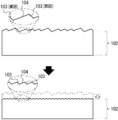
- the SiC single crystal 10 that has undergone mechanical processing for example, slicing, grinding / polishing
- laser processing includes a strain layer 101 into which processing damages such as scratches 1011 and latent scratches 1012 and strains 1013 have been introduced. It has a bulk layer 102 in which such processing damage is not introduced (see FIG. 8).
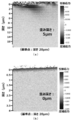
- this strain layer 101 can be confirmed by the SEM-EBSD method, TEM, ⁇ XRD, Raman spectroscopy, or the like. In order to grow a high-quality SiC ingot, it is preferable to remove the strain layer 101 to expose the bulk layer 102 to which no processing damage has been introduced.
- a step-terrace structure is confirmed on the surface of the SiC single crystal 10 flattened at the atomic level.
- This step-terrace structure is a staircase structure in which step 103, which is a stepped portion having one or more molecular layers, and terrace 104, which is a flat portion where the ⁇ 0001 ⁇ surface is exposed, are alternately arranged (FIG. 10 and FIG. See FIG. 12).
- step 103 one molecular layer (0.25 nm) is the minimum height (minimum unit), and various step heights are formed by overlapping a plurality of the single molecular layers.
- MSB the one in which step 103 is bundled (bunched) to become huge and has a height exceeding one unit cell of each polytype.
- the MSB refers to step 103 that bunched beyond the 4 molecular layer (5 or more molecular layers). Further, in the case of 6H-SiC, it refers to step 103 bunching beyond the 6-layer (7-layer or more).
- the heat treatment step S1 is a step of heat-treating the SiC single crystal 10 in an atmosphere containing Si element and C element.
- the SiC seed crystal 11 that has undergone the heat treatment step S1 has a surface in which at least one or more of strain (strain layer 101), BPD, and MSB is reduced. Therefore, in the ingot growth step S2, which is a later step, it is possible to prevent the SiC ingot 12 from inheriting the distortion caused by the strain of the SiC seed crystal 11, the BPD, and the MSB. That is, it is possible to manufacture a high quality SiC ingot 12.
- the heat treatment step S1 is an etching step of transporting the SiC element and the C element from the SiC single crystal body 10 to the SiC material to etch the SiC single crystal body 10, and conversely, the SiC single crystal body from the SiC material.
- a crystal growth step of transporting the Si element and the C element to the 10 to grow the SiC single crystal 10 into a crystal may be included.
- the specific embodiment of the heat treatment step S1 is not particularly limited as long as it is a step capable of removing or reducing the strain layer 101, BPD and MSB contained in the SiC single crystal body 10.
- the temperature gradient and the chemical potential difference between the SiC single crystal body 10 and the SiC material can be adopted.
- the SiC material is composed of SiC that can receive or transfer Si element and C element to and from the SiC single crystal body 10 by heating it relative to the SiC single crystal body 10.
- a container made of SiC (main body container 20) or a substrate made of SiC (SiC member) can be adopted.
- the crystal polymorph of this SiC material any polymorphic type can be adopted, and polycrystalline SiC may be adopted.
- the SiC single crystal 10 and the SiC material are preferably placed in a semi-closed space and heated.
- the surface of the SiC single crystal 10 was etched and grown, and at least one or more of the strain layers 101, BPD and MSB was reduced.
- a surface can be formed.
- the term "quasi-closed space” as used herein refers to a space in which the inside of the container can be evacuated, but at least a part of the vapor generated in the container can be confined.
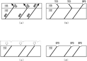
- a preferred embodiment of the heat treatment step S1 can be roughly divided into an etching step of etching the surface of the SiC single crystal body 10 and a crystal growth step of growing a single crystal SiC crystal on the SiC single crystal body 10 (FIG. 6). 2).
- FIG. 3 is an explanatory diagram showing an outline of the etching process.
- the SiC single crystal 10 is placed in a semi-closed space where the SiC material is exposed and heated in a temperature range of 1400 ° C. or higher and 2300 ° C. or lower, so that the reactions 1) to 5) below are sustained. It is considered that the etching proceeds as a result.
- the Si atom sublimation step of thermally sublimating the Si atom from the surface of the SiC single crystal body 10 and the C atom remaining on the surface of the SiC single crystal body 10 and the Si vapor in the semi-closed space are combined. It includes a C atom sublimation step of sublimating from the surface of the SiC single crystal body 10 by reacting.
- the etching step heats the SiC single crystal 10 on the high temperature side of the temperature gradient and the SiC material on the low temperature side of the temperature gradient.
- an etching space X is formed between the SiC single crystal 10 and the SiC material, and the surface of the SiC single crystal 10 can be etched using the temperature gradient as a driving force.
- Crystal growth process According to the crystal growth step (step located on the right side of FIG. 2), the BPD existing on the surface of the SiC single crystal 10 is converted into another dislocation, and the BPD exposed on the surface of the SiC seed crystal 11 is removed or reduced. be able to. Further, the MSB on the surface of the SiC seed crystal 11 can be removed or reduced.
- FIG. 4 is an explanatory diagram showing an outline of the crystal growth process.
- the reaction of 1) to 5) below is sustained by arranging the SiC single crystal 10 in a semi-closed space where the SiC material is exposed and heating in a temperature range of 1400 ° C. or higher and 2300 ° C. or lower. It is considered that the crystal growth progresses as a result.
- the crystal growth step sublimates the C atoms remaining on the surface of the SiC material by reacting the Si atom sublimation step of thermally sublimating the Si atoms from the surface of the SiC material with the Si vapor in the semi-closed space.
- the raw material is transferred to the C atom sublimation step, the raw material transporting step of transporting the raw materials (Si atom and C atom) to the surface of the SiC single crystal 10 using the temperature gradient and the chemical potential difference as the driving force, and the step of the SiC single crystal 10.
- the SiC material is heated on the high temperature side of the temperature gradient, and the SiC single crystal 10 is heated on the low temperature side of the temperature gradient.
- the raw material supply space Y is formed between the SiC single crystal 10 and the SiC material, and the SiC single crystal 10 can be crystal-grown by using the temperature gradient as a driving force.
- the partial pressure difference (chemical potential difference) generated on the surfaces of the polycrystalline SiC and the single crystal SiC is transported as a raw material. Crystals can be grown as a driving force for. In this case, a temperature gradient may or may not be provided.
- the heat treatment step S1 has been roughly divided into an etching step and a crystal growth step.
- the heat treatment step S1 can be classified into two types from the viewpoint of the environment for heating the SiC single crystal body 10.
- the SiC single crystal 10 is heated in a SiC-Si equilibrium vapor pressure environment and in a SiC-C equilibrium vapor pressure environment. It can be classified into the form to be used and the form to be used.
- the SiC-Si equilibrium vapor pressure environment refers to a vapor pressure environment when SiC (solid) and Si (liquid phase) are in a phase equilibrium state via a gas phase.
- the SiC-C equilibrium vapor pressure environment refers to a vapor pressure environment when SiC (solid phase) and C (solid phase) are in a phase equilibrium state via a gas phase.
- the SiC-Si equilibrium vapor pressure environment and the SiC-C equilibrium vapor pressure environment in the present specification include a near thermal equilibrium vapor pressure environment that satisfies the relationship between the growth rate and the growth temperature derived from the theoretical thermal equilibrium environment.
- the atomic number ratio Si / C in the gas phase of the SiC-Si equilibrium vapor pressure environment is larger than the atomic number ratio Si / C in the gas phase of the SiC-C equilibrium vapor pressure environment.
- the SiC-Si equilibrium vapor pressure environment can be formed by arranging the SiC single crystal 10 in a semi-closed space having an atomic number ratio of Si / C exceeding 1 and heating it.
- a SiC container main body container 20
- SiC single crystal 10 having a chemical ratio of 1: 1 and a SiC material having a chemical ratio of 1: 1.
- the Si steam supply source Si pellets or the like
- the atomic number ratio Si / C in the semi-closed space exceeds 1.
- the SiC-C equilibrium vapor pressure environment can be formed by arranging the SiC single crystal 10 in a semi-closed space having an atomic number ratio of Si / C of 1 or less and heating it.
- a SiC container main body container 20
- a SiC single crystal 10 having a chemical ratio of 1: 1 and a SiC material having a chemical ratio of 1: 1.
- the atomic number ratio Si / C in the main body container 20 becomes 1.
- a C steam supply source (C pellet or the like) may be arranged to set the atomic number ratio Si / C to 1 or less.
- the heat treatment step S1 is (1) an etching step or a crystal growth step, (2) heat treatment under a SiC-Si equilibrium vapor pressure environment, or a SiC-C equilibrium vapor pressure environment. It can be classified from the viewpoint of whether to perform heat treatment below. By associating this combination of classifications with effects, it can be classified into the following four types.
- the strain layer 101 of the SiC single crystal 10 can be removed by etching, and MSB is formed on the surface after etching. Therefore, it is classified as the etching bunching step S111 (lower left of FIG. 2).
- the strain layer 101 of the SiC single crystal 10 can be removed by etching, and MSB is not formed on the surface after etching. Therefore, it is classified as the etching flattening step S121 (upper left of FIG. 2).
- the crystal growth step is performed in a SiC-Si equilibrium vapor pressure environment, it is possible to form a growth layer 105 on which the MSB is reduced or removed on the SiC single crystal body 10. Therefore, it is classified as the growth flattening step S122 (upper right of FIG. 2).
- the MSB can be removed or reduced in the etching flattening step S121 and the growth flattening step S122, they are collectively classified as the flattening step S12 (upper side of FIG. 2).
- the crystal growth step is performed in a SiC-C equilibrium vapor pressure environment, it is possible to remove or reduce BPD in the growth layer 105. Therefore, it is classified as the basal plane dislocation reduction step S13 (lower right of FIG. 2).
- the main body container 20 preferably has a structure in which the SiC material is exposed in the internal space.
- the entire main body container 20 is made of a SiC material (polycrystalline SiC). By heating the main body container 20 made of such a material, an atmosphere containing Si element and C element can be generated inside (semi-closed space).
- the environment inside the heat-treated main body container 20 be a vapor pressure environment of a mixed system of a gas phase species containing a Si element and a gas phase species containing a C element.
- the gas phase species containing the Si element include Si, Si 2 , Si 3 , Si 2 C, SiC 2 , and SiC.
- the gas phase species containing the C element include Si 2 C, SiC 2 , SiC and C. That is, the SiC gas is present in the main container 20.
- this configuration can be adopted as long as the vapor pressure of the vapor phase species containing the Si element and the vapor pressure species containing the C element is generated in the internal space during the heat treatment of the main container 20.
- a configuration in which the SiC material is exposed on a part of the inner surface or a configuration in which the SiC material (such as a SiC substrate) is separately arranged in the main body container 20 can be shown.
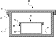
- the SiC single crystal 10 is housed inside the main body container 20 and the main body container 20 is heated so that a temperature gradient is formed inside.
- the apparatus configuration main container 20, heating furnace 30, high melting point container 40
- the main body container 20 is a fitting container including an upper container 21 and a lower container 22 that can be fitted to each other.
- a minute gap 23 is formed in the fitting portion between the upper container 21 and the lower container 22, and the inside of the main container 20 can be exhausted (evacuated) from the gap 23. That is, the inside of the main body container 20 is a semi-closed space.
- the heating furnace 30 has a configuration in which the main body container 20 can be heated by providing a temperature gradient in an atmosphere containing Si element.
- the heating furnace 30 includes a main heating chamber 31 capable of heating an object to be treated (SiC single crystal 10 or the like) to a temperature of 1000 ° C. or higher and 2300 ° C. or lower.
- a preheating chamber 32 capable of preheating the object to be processed to a temperature of 500 ° C. or higher
- a melting point container 40 capable of accommodating the main body container 20, and the melting point container 40 are moved from the preheating chamber 32 to the main heating chamber 31. It is provided with a possible moving means 33 (moving table).
- the heating chamber 31 is formed in a regular hexagonal shape in a plan sectional view, and the melting point container 40 is arranged inside the heating chamber 31.
- a heating heater 34 (mesh heater) is provided inside the heating chamber 31.
- a multilayer heat-reflecting metal plate is fixed to the side wall or ceiling of the heating chamber 31 (not shown). The multilayer heat-reflecting metal plate is configured to reflect the heat of the heating heater 34 toward the substantially central portion of the main heating chamber 31.
- the heating heater 34 is arranged so as to surround the melting point container 40 in which the object to be processed is housed, and further, the multilayer heat-reflecting metal plate is arranged outside the heating heater 34, whereby 1000 ° C.
- the temperature can be raised to 2300 ° C. or lower.
- a resistance heating type heater or a high frequency induction heating type heater can be used as the heating heater 34.
- the heating heater 34 may adopt a configuration capable of forming a temperature gradient in the melting point container 40.
- the heating heater 34 may be configured so that many heaters are arranged on the upper side (or lower side). Further, the heating heater 34 may be configured so that the width increases toward the upper side (or the lower side). Alternatively, the heating heater 34 may be configured so that the electric power supplied can be increased toward the upper side (or the lower side).
- a vacuum forming valve 35 for exhausting the inside of the main heating chamber 31, an inert gas injection valve 36 for introducing an inert gas into the main heating chamber 31, and the main heating chamber 31
- a vacuum gauge 37 for measuring the degree of vacuum inside is connected.
- the vacuum forming valve 35 is connected to a vacuum drawing pump that exhausts the inside of the main heating chamber 31 to create a vacuum (not shown). With the vacuum forming valve 35 and the vacuum pulling pump, the degree of vacuum in the heating chamber 31 can be adjusted to, for example, 10 Pa or less, more preferably 1 Pa or less, still more preferably 10 -3 Pa or less. As this evacuation pump, a turbo molecular pump can be exemplified.
- the Inert gas injection valve 36 is connected to the Inactive gas supply source (not shown). With the inert gas injection valve 36 and the inert gas supply source, the inert gas can be introduced into the heating chamber 31 in the range of 10-5 to 10000 Pa. As the inert gas, Ar, He, N 2, or the like can be selected.
- the preheating chamber 32 is connected to the main heating chamber 31, and is configured so that the melting point container 40 can be moved by the moving means 33.
- the preheating chamber 32 of the present embodiment is configured so that the temperature can be raised by the residual heat of the heating heater 34 of the main heating chamber 31. For example, when the temperature of the main heating chamber 31 is raised to 2000 ° C., the temperature of the preheating chamber 32 is raised to about 1000 ° C., and the object to be treated (SiC single crystal 10, main body container 20, high melting point container 40, etc.) Can be degassed.
- the moving means 33 is configured to be movable between the main heating chamber 31 and the preheating chamber 32 on which the melting point container 40 is placed. Since the transfer between the main heating chamber 31 and the preheating chamber 32 by the moving means 33 is completed in about 1 minute at the shortest, the temperature can be raised or lowered at 1 to 1000 ° C./min. In this way, since the manufacturing apparatus can rapidly raise the temperature and lower the temperature, it is possible to observe a surface shape that does not have a history of low-temperature growth during raising and lowering, which was difficult with the conventional apparatus. is there. Further, in FIG. 6, the preheating chamber 32 is arranged below the main heating chamber 31, but the present invention is not limited to this, and the preheating chamber 32 may be arranged in any direction.
- the moving means 33 is a moving table on which the high melting point container 40 is placed. A small amount of heat is released from the contact portion between the moving table and the melting point container 40. As a result, a temperature gradient can be formed in the high melting point container 40.
- a temperature gradient is provided so that the temperature decreases from the upper container 41 to the lower container 42 of the melting point container 40. ..
- the direction of this temperature gradient can be set to any direction by changing the position of the contact portion between the moving table and the melting point container 40.
- the temperature gradient is provided so that the temperature rises from the upper container 41 of the high melting point container 40 toward the lower container 42. It is desirable that this temperature gradient is formed along the front and back directions of the SiC single crystal body 10. Further, as described above, a temperature gradient may be formed depending on the configuration of the heating heater 34.
- the atmosphere containing the Si element in the heating furnace 30 is formed by using the high melting point container 40 and the Si steam supply source 44.
- any method capable of forming an atmosphere containing a Si element around the main body container 20 can be adopted in the apparatus for producing the SiC seed crystal 11.
- the melting point container 40 is configured to include a melting point material.
- a general purpose heat-resistant member C, W is a refractory metal, Re, Os, Ta, Mo , Ta 9 C 8 is a carbide, HfC, TaC, NbC, ZrC , Ta 2 C, TiC, WC, MoC, a nitride HfN, TaN, BN, Ta 2 N, ZrN, TiN, HfB 2, TaB 2, ZrB 2, NB 2, TiB 2 is a boride, it can be exemplified polycrystalline SiC.
- the high melting point container 40 is a fitting container including an upper container 41 and a lower container 42 that can be fitted to each other, and is configured to be able to accommodate the main body container 20.
- a minute gap 43 is formed in the fitting portion between the upper container 41 and the lower container 42, and the inside of the high melting point container 40 can be exhausted (evacuated) from the gap 43. That is, like the main container 20, the inside of the melting point container 40 is preferably a semi-closed space.
- the high melting point container 40 has a Si steam supply source 44 capable of supplying Si steam in the high melting point container 40.
- the Si steam supply source 44 may be configured to generate Si steam in the melting point container 40 during heat treatment.
- Examples of the Si vapor supply source 44 include solid Si (Si pellets such as single crystal Si pieces and Si powder) and Si compounds.
- TaC is adopted as the material of the melting point container 40
- tantalum silicide is adopted as the Si vapor supply source 44. That is, as shown in FIG. 5, a tantalum silicide layer is formed inside the melting point container 40, and Si vapor is supplied from the tantalum silicide layer into the container during the heat treatment. As a result, a Si vapor pressure environment is formed in the high melting point container 40, and the main body container 20 can be heated in an atmosphere containing Si elements. In addition to this, any configuration can be adopted as long as an atmosphere containing Si element is formed in the melting point container 40 during the heat treatment.
- the main body container 20 contains the Si element from the inside of the main body container 20 by heating in an atmosphere containing the Si element (for example, a Si vapor pressure environment). It is possible to suppress the exhaust of vapor phase species. That is, the environment inside the main body container 20 is maintained by balancing the vapor pressure of the vapor phase species containing the Si element inside the main body container 20 and the vapor pressure of the gas phase species containing the Si element outside the main body container 20. be able to.
- an atmosphere containing the Si element for example, a Si vapor pressure environment.
- the main body container 20 is composed of polycrystalline SiC. With such a configuration, when the main body container 20 is heated by using the heating furnace 30, steam of a gas phase type containing Si element and a gas phase type containing C element is generated in the main body container 20. Can be done.
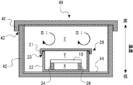
- the outline of the device configuration for realizing the etching process is shown on the left side of FIG. 7.
- the SiC single crystal 10 is located on the high temperature side of the temperature gradient, and the SiC material (a part of the main body container 20) is located on the low temperature side of the temperature gradient.
- It has a space X. That is, the etching space X is formed by arranging the SiC single crystal 10 at a position where the temperature is higher than that of the SiC material (for example, the bottom surface of the lower container 22) due to the temperature gradient formed by the heating furnace 30. There is.
- the etching space X is a space for transporting Si atoms and C atoms on the surface of the SiC single crystal body 10 to the main body container 20 by using a temperature difference provided between the SiC single crystal body 10 and the main body container 20 as a driving force. For example, when the temperature on the surface of the SiC single crystal 10 and the temperature on the bottom surface of the lower container 22 facing the surface are compared, the temperature on the surface side of the SiC single crystal 10 is higher, and the temperature on the bottom surface side of the lower container 22 is higher. The main body container 20 is heated so that the temperature becomes low (see the left side of FIG. 7).
- etching space X a space having a temperature difference between the surface of the SiC single crystal 10 and the bottom surface of the lower container 22
- Si atoms and C atoms are transported using the temperature difference as a driving force.
- the surface of the SiC single crystal 10 can be etched (the white arrow on the right side of FIG. 7 is the direction of transportation).
- the main body container 20 may have a substrate holder 24 provided between the SiC single crystal body 10 and the main body container 20.
- the heating furnace 30 has a structure capable of heating by forming a temperature gradient such that the temperature decreases from the upper container 21 to the lower container 22 of the main container 20. Therefore, a substrate holder 24 capable of holding the SiC single crystal 10 is provided between the SiC single crystal 10 and the lower container 22, and an etching space X is formed between the SiC single crystal 10 and the lower container 22. You may.
- the substrate holder 24 may have a structure capable of holding at least a part of the SiC single crystal body 10 in the hollow of the main body container 20.
- any conventional support means such as one-point support, three-point support, a configuration for supporting the outer peripheral edge, or a configuration for sandwiching a part thereof can be naturally adopted.
- the substrate holder 24 may not be provided depending on the direction of the temperature gradient of the heating furnace 30.
- the heating furnace 30 forms a temperature gradient so that the temperature decreases from the lower container 22 toward the upper container 21
- a SiC single crystal is formed on the bottom surface of the lower container 22 (without providing the substrate holder 24). 10 may be arranged.
- the SiC single crystal 10 is located on the low temperature side of the temperature gradient, and the SiC material (a part of the main body container 20) is located on the high temperature side of the temperature gradient. It has a raw material supply space Y. That is, the raw material supply space Y is formed by arranging the SiC single crystal 10 at a position lower than the SiC material (for example, the top surface of the upper container 21) due to the temperature gradient formed by the heating furnace 30. Has been done.
- the raw material supply space Y in addition to the SiC single crystal body 10, there are a Si atom supply source and a C atom supply source as raw materials. Then, by heating these, Si atoms and C atoms which are the raw materials of the SiC single crystal 10 are supplied into the raw material supply space Y. The Si atoms and C atoms are transported to the surface of the SiC single crystal body 10 and recrystallized to form a growth layer 105 (the black arrow on the right side of FIG. 7 indicates the direction of transport).
- the main body container 20 is formed of polycrystalline SiC (Poly-SiC), so that the main body container 20 itself is used as a Si atom supply source and a C atom supply source.
- Si atom supply source and the C atom supply source a material capable of supplying Si atoms such as a Si substrate, a material capable of supplying C atoms such as graphite, and Si atoms and C atoms such as a SiC substrate can be supplied.
- the material can be adopted.
- the arrangement of the Si atom supply source and the C atom supply source is not limited to this form, and any form may be used as long as the Si atom and the C atom can be supplied into the raw material supply space Y.
- the vapor pressure difference (chemical potential difference) between the polycrystalline SiC (raw material) and the single crystal SiC (SiC single crystal body 10) can be used as the growth driving force.
- a temperature gradient is provided so that the temperature decreases toward the SiC single crystal body 10.
- the transport of Si atoms and C atoms to the SiC single crystal 10 occurs, so that the growth rate of the growth layer 105 increases (the black arrow on the right side of FIG. 7 indicates the direction of transport). ..
- the Si atom supply source and the C atom supply source may be brought close to the SiC single crystal body 10.
- the Si atom supply source and the polycrystalline SiC upper container 21 serving as the C atom supply source can be arranged in parallel with the SiC single crystal body 10.
- the distance between the surface of the SiC single crystal 10 and the top surface of the upper container 21 is preferably set to 100 mm or less, more preferably 10 mm or less, still more preferably 2.7 mm or less. Further, it is preferably set to 0.7 mm or more, more preferably 1.2 mm or more, and further preferably 1.7 mm or more.
- the etching space X and the raw material supply space Y are exhausted (evacuated) through the Si vapor pressure space Z. That is, the main body container 20 having the etching space X and / or the raw material supply space Y is arranged in the melting point container 40 having the Si vapor pressure space Z, and the SiC single crystal 10 is further arranged in the main body container 20. Is desirable.
- the SiC-Si equilibrium vapor pressure environment can be formed by arranging the SiC single crystal 10 in a semi-closed space having an atomic number ratio of more than 1 and heating it.
- the SiC single crystal body 10 satisfying the chemical quantity theory ratio 1: 1 and the chemical quantity are contained in the main body container 20 of polycrystalline SiC satisfying the chemical quantity theory ratio 1: 1.
- the atomic number ratio Si / C in the main body container 20 is 1. It will exceed.
- the inside of the main body container 20 approaches a SiC-Si equilibrium vapor pressure environment.
- the outline of the device configuration for realizing the SiC-C equilibrium vapor pressure environment is shown on the lower side of FIG. 7.
- the SiC-C equilibrium vapor pressure environment can be formed by arranging the SiC single crystal 10 in a semi-closed space having an atomic number ratio of 1 or less and heating it.
- a SiC single crystal body 10 satisfying the chemical quantity theory ratio 1: 1 and a chemical quantity are contained in the main body container 20 of the polycrystalline SiC satisfying the chemical quantity theory ratio 1: 1.
- the SiC substrate holder 24 satisfying the ratio of 1: 1 is arranged, the number of atoms ratio Si / C in the main body container 20 is 1 or 1 or less.
- the inside of the main body container 20 approaches the SiC-C equilibrium vapor pressure environment.
- the C steam supply source may be separately arranged, or the main body container 20 including the C steam supply source and the substrate holder 24 may be adopted. ..
- the C steam supply source include solid C (C pellets such as C substrate and C powder) and C compounds.
- the SiC seed crystal 11 from which the strain layer 101 of the SiC single crystal 10 has been removed can be obtained. Further, if the heat treatment step S1 for growing crystals in a SiC-C equilibrium vapor pressure environment is performed, a high-quality SiC seed crystal 11 having a growth layer 105 from which BPD has been removed or reduced can be obtained.
- the heat treatment step S1 for etching or crystal growth is performed in a SiC-Si equilibrium vapor pressure environment, the surface of the SiC single crystal 10 can be flattened. That is, it is possible to obtain a SiC seed crystal 11 in which the MSB is removed or reduced. As a result, it is possible to prevent defects caused by the MSB or the like from being inherited by the SiC ingot by the ingot growth step S2, which is a later step.
- the strain layer removing step S11 is a step of removing the strain layer 101 introduced into the SiC single crystal body 10.
- the strain layer removing step S11 will be described, but the description will be omitted if it overlaps with the general description of the heat treatment step S1 described above.
- the SiC single crystal body 10 and the SiC material are placed in a semi-closed space having an atomic number ratio of Si / C of 1 or less. Is a step of heating the SiC single crystal body 10 so as to be on the high temperature side and the SiC material on the low temperature side (etching bunching step S111).
- the SiC single crystal body 10 and the SiC material are arranged so as to face each other in a semi-closed space in which the atomic number ratio Si / C exceeds 1.
- the step of heating the SiC single crystal 10 to the high temperature side and the SiC material to the low temperature side (etching flattening step S121).
- the SiC single crystal 10 and the SiC material are arranged so as to face each other, and the SiC single crystal 10 is on the high temperature side and the SiC material is placed in a SiC-Si equilibrium vapor pressure environment or a SiC-C equilibrium vapor pressure environment. Is a step of heating so that is on the low temperature side.
- the SiC single crystal 10 arranged on the high temperature side of the temperature gradient and a part of the main body container 20 arranged on the low temperature side of the temperature gradient are heat-treated so as to face each other. Atoms are transported from 10 to the main body container 20 to achieve etching of the SiC single crystal body 10.
- the surface of the SiC single crystal 10 and the bottom surface of the main body container 20 having a temperature lower than this surface are arranged so as to face each other, so that an etching space X is formed between them.
- this etching space X atoms are transported by using the temperature gradient formed by the heating furnace 30 as a driving force, and as a result, the SiC single crystal 10 can be etched.
- the back surface of the SiC single crystal body 10 and the top surface of the main body container 20 having a temperature higher than this back surface are arranged relative to each other.
- a raw material supply space Y may be formed between them.
- the raw material is transported by using the temperature gradient formed by the heating furnace 30 as a driving force, and as a result, the growth layer 105 can be formed on the back surface side of the SiC single crystal body 10.
- the strain layer removing step S11 a configuration may be adopted in which the raw material supply space Y is not formed by bringing the back surface side of the SiC single crystal body 10 into contact with the top surface of the main body container 20.
- the main body container 20 is arranged in the Si vapor pressure space Z in which an atmosphere containing a Si element is formed.
- the main body container 20 is arranged in the Si vapor pressure space Z, and the inside of the main body container 20 is exhausted (evacuated) through the space of the Si vapor pressure environment, so that Si atoms are discharged from the inside of the main body container 20. It can be suppressed from decreasing. As a result, the preferable atomic number ratio Si / C in the main body container can be maintained for a long time.
- the etching temperature in the strain layer removing step S11 is preferably set in the range of 1400 to 2300 ° C, and more preferably set in the range of 1600 to 2000 ° C.
- the etching rate in the strain layer removing step S11 can be controlled by the above temperature range, and can be selected in the range of 0.001 to 2 ⁇ m / min.
- the etching amount in the strain layer removing step S11 can be adopted as long as it is an etching amount capable of removing the strain layer 101 of the SiC single crystal body 10. As the etching amount, 0.1 ⁇ m or more and 20 ⁇ m or less can be exemplified, but it can be applied as needed.
- the etching time in the strain layer removing step S11 can be set to an arbitrary time so as to obtain a desired etching amount. For example, when the etching rate is 1 ⁇ m / min and the etching amount is desired to be 1 ⁇ m, the etching time is 1 minute.
- the temperature gradient in the strain layer removing step S11 is set in the range of 0.1 to 5 ° C./mm in the etching space X.
- the SiC seed crystal 11 in which the strain layer 101 is removed or reduced can be produced.
- the flattening step S12 is a step of decomposing and removing the MSB formed on the surface of the SiC seed crystal 11 as shown in FIGS. 10 and 12.
- the etching flattening step S121 and the growth flattening step S122 are preferably exemplified in the flattening step S12.
- the flattening step S12 will be described, but the description will be omitted if it overlaps with the general description of the heat treatment step S1 described above.
- the etching flattening step S121 is a step of reducing or removing the MSB by etching the surface of the SiC single crystal 10 on which the MSB is formed.
- the SiC single crystal body 10 and the SiC material are placed in a semi-closed space having an atomic number ratio of Si / C of more than 1.
- This is a step in which the SiC single crystals 10 are arranged so as to face each other and heated so that the SiC single crystal 10 is on the high temperature side and the SiC material is on the low temperature side.
- the apparatus configuration for realizing the etching flattening step S121 is such that the Si vapor supply source 25 is further arranged in the main body container 20 of the strain layer removing step S11.
- the Si steam supply source 25 By arranging the Si steam supply source 25, the SiC single crystal 10 can be heated in a SiC-Si equilibrium vapor pressure environment.
- the description of the portion overlapping with the general description of the strain layer removing step S11 will be omitted as appropriate.
- the etching temperature in the etching flattening step S121 is preferably set in the range of 1400 to 2300 ° C, more preferably in the range of 1600 to 2000 ° C.
- the etching rate in the etching flattening step S121 can be controlled by the above temperature range, and can be selected in the range of 0.001 to 2 ⁇ m / min.
- the etching amount in the etching flattening step S121 can be adopted as long as it is an etching amount capable of decomposing the MSB of the SiC single crystal body 10. As the etching amount, 0.1 ⁇ m or more and 20 ⁇ m or less can be exemplified.
- the etching time in the etching flattening step S121 can be set to an arbitrary time so as to obtain a desired etching amount. For example, when the etching rate is 1 ⁇ m / min and the etching amount is desired to be 1 ⁇ m, the etching time is 1 minute.
- the temperature gradient in the etching flattening step S121 is set in the range of 0.1 to 5 ° C./mm in the etching space X.
- the etching flattening step S121 by etching the surface of the SiC single crystal body 10, it is possible to produce the SiC seed crystal 11 in which the MSB is removed or reduced.
- the growth flattening step S122 is a step of forming a growth layer 105 in which the MSB is reduced or removed by growing crystals on the surface of the SiC single crystal 10 on which the MSB is formed.
- the SiC single crystal 10 and the SiC material are placed in a semi-closed space having an atomic number ratio of Si / C of more than 1.
- This is a step in which the SiC single crystals 10 are arranged so as to face each other and heated so that the SiC single crystal 10 is on the low temperature side and the SiC material is on the high temperature side.
- the surface of the SiC single crystal 10 and the top surface of the main body container 20 having a temperature higher than this surface are arranged so as to face each other, so that the raw material supply space Y is formed between them.
- the raw material is transported by the temperature gradient formed by the heating furnace 30 and the chemical potential difference between the SiC single crystal 10 and the SiC material as a driving force, and as a result, the surface of the SiC single crystal 10 is transported.
- the growth layer 105 can be formed.
- the apparatus configuration for realizing the growth flattening step S122 is a configuration in which the Si vapor supply source 25 is further arranged in the main body container 20 as in the etching flattening step S121.
- the description of the parts that overlap with the general description of the etching flattening step S121 described above will be omitted.
- the heating temperature in the growth flattening step S122 is preferably set in the range of 1400 to 2200 ° C, more preferably in the range of 1600 to 2000 ° C.
- the growth rate in the growth flattening step S122 can be controlled by the above temperature range and can be selected in the range of 0.001 to 1 ⁇ m / min.
- the amount of growth in the growth flattening step S122 is preferably 5 ⁇ m or more, and more preferably 8 ⁇ m or more.
- the growth time in the growth flattening step S122 can be set to an arbitrary time so as to achieve a desired growth amount. For example, when the growth rate is 10 nm / min and the amount of growth is desired to be 10 ⁇ m, the growth time is 100 minutes.
- the degree of vacuum (main heating chamber 31) in the growth flattening step S122 is 10-5 to 10 Pa, more preferably 10 -3 to 1 Pa.
- an inert gas during growth. Ar or the like can be selected as the inert gas, and the degree of vacuum of the heating furnace 30 (main heating chamber 31) can be adjusted by introducing the inert gas in the range of 10-5 to 10000 Pa. it can.
- the SiC seed crystal 11 in which the MSB is removed or reduced is produced by growing the growth layer 105 having no MSB on the surface of the SiC single crystal 10. can do.
- the basal dislocation reduction step S13 is a step of forming a growth layer 105 in which BPD is removed or reduced by growing crystals under the condition that the terrace width W of the SiC single crystal 10 is increased. is there.
- the description of the parts that overlap with the general description of the heat treatment step S1 described above will be omitted.
- the SiC single crystal body 10 and the SiC material are contained in a semi-closed space having an atomic number ratio of Si / C of 1 or less.
- This is a step of heating the SiC single crystal body 10 so as to be on the low temperature side and the SiC material on the high temperature side.
- the apparatus configuration for realizing the basal dislocation reduction step S13 is the SiC single crystal 10 arranged on the low temperature side of the temperature gradient and the SiC single crystal 10 arranged on the high temperature side of the temperature gradient.
- the raw material is transported from the main body container 20 to the SiC single crystal body 10 to form the growth layer 105.
- the Si vapor supply source 25 is not arranged. It should be noted that the description of the parts that overlap with the general description of the growth flattening step S122 described above will be omitted.
- the heating temperature in the basal dislocation reduction step S13 is preferably set in the range of 1400 to 2200 ° C, more preferably in the range of 1600 to 2000 ° C.
- the growth rate in the basal dislocation reduction step S13 can be controlled by the above temperature region and the growth environment, and can be selected in the range of 0.001 to 1 ⁇ m / min.
- the amount of growth in the basal dislocation reduction step S13 is preferably 5 ⁇ m or more, and more preferably 8 ⁇ m or more.
- the growth time in the basal dislocation reduction step S13 can be set to an arbitrary time so as to achieve a desired growth amount. For example, when the growth rate is 10 nm / min and the amount of growth is desired to be 10 ⁇ m, the growth time is 100 minutes.
- the degree of vacuum (main heating chamber 31) in the basal dislocation reduction step S13 is 10-5 to 10 Pa, more preferably 10 -3 to 1 Pa.
- an inert gas during growth. Ar or the like can be selected as the inert gas, and the degree of vacuum of the heating furnace 30 (main heating chamber 31) can be adjusted by introducing the inert gas in the range of 10-5 to 10000 Pa. it can.
- the conversion rate (BPD conversion rate) at which BPD is converted into other defects / dislocations is improved by growing the terrace 104 under the condition of increasing the width (terrace width W).
- the BPD density in the growth layer 105 can be reduced or removed.
- the condition for increasing the terrace width W is a condition for increasing the terrace width W2 after growth as compared with the terrace width W1 before growth, for example, growing in a SiC-C equilibrium vapor pressure environment or a C-rich environment. It can be realized by.
- the basal plane dislocation reduction step S13 is performed after the flattening step S12. That is, when comparing the width of the terrace 104 on the surface on which the MSB is not formed and the width of the terrace 104 on the surface on which the MSB is formed, the terrace 104 on the surface on which the MSB is not formed is wider than the terrace 104. Is narrow. Therefore, the BPD conversion rate can be improved by growing the growth layer 105 under the condition that the MSB is formed after the decomposition of the MSB.
- FIG. 16A shows a mode in which the strain layer removing step S11 is performed as the heat treatment step S1 and the SiC seed crystal 11 thus obtained is subjected to the ingot growth step S2.
- the SiC seed crystal 11 from which the strain layer 101 has been removed can be obtained. That is, it is possible to prevent the defects caused by the strain layer 101 from being inherited by the SiC ingot 12.
- either the etching bunching step S111 or the etching flattening step S121 can be adopted.
- the strain layer 101 can be removed and the MSB can be removed or reduced at the same time.
- FIG. 16B shows a mode in which the flattening step S12 is performed after the strain layer removing step S11. According to such a form, the SiC seed crystal 11 having no strain layer 101 and MSB on its surface can be produced. This makes it possible to manufacture a high quality SiC ingot 12.
- FIG. 16C shows a mode in which the basal plane dislocation reduction step S13 is performed after the strain layer removing step S11 and the flattening step S12.
- FIG. 16D is a form in which the flattening step S12 is further performed after the basal plane dislocation reduction step S13 in the form shown in FIG. 16C.
- any of the etching flattening step S121 and the growth flattening step S122 can be adopted.
- the heat treatment step S1 is selected from a strain layer removing step S11 (etching bunching step S111 or etching flattening step S121), a flattening step S12 (etching flattening step S121 or growth flattening step S122), and a basal plane rearrangement reduction step S13.
- a strain layer removing step S11 etching bunching step S111 or etching flattening step S121
- a flattening step S12 etching flattening step S121 or growth flattening step S122
- a basal plane rearrangement reduction step S13 When the form includes two or more types, the two or more types of steps can be heat-treated with the same apparatus configuration.
- Examples of the container in which the plurality of heat treatment steps S1 are performed include a container that generates an atmosphere of Si element and C element in the internal space, specifically, a main body container 20. As described above, by using the main body container 20 and the like, even if the heat treatment step S1 includes a plurality of steps, all of them can be completed in the same container, so that the work can be expected to be simplified. Further, since etching and crystal growth can be performed in the same device system, it is not necessary to introduce a plurality of devices, which is very advantageous in industry.
- the present invention also relates to a SiC seed crystal 11 produced through the heat treatment step S1.
- the surface of the SiC seed crystal 11 of the present invention does not contain factors such as strain layer 101, BPD, and MSB that adversely affect ingot growth in the heat treatment step S1. Therefore, according to the SiC seed crystal 11 of the present invention, it is possible to grow a higher quality SiC ingot.
- the SiC seed crystal 11 is preferably characterized by having a growth layer 105 on its surface that does not contain BPD.
- the thickness of the growth layer 105 containing no BPD is preferably 0.001 ⁇ m or more, more preferably 0.01 ⁇ m or more, and further preferably 0.1 ⁇ m or more. When the thickness of the layer containing no BPD is within the above range, it is possible to suppress the propagation of BPD present in the SiC seed crystal 11 to the ingot in the growth step of growing SiC on the SiC seed crystal 11. ..
- the diameter of the SiC seed crystal 11 of the present invention is not particularly limited, and is preferably 6 inches or more, more preferably 8 inches or more, and further preferably 12 inches or more.
- the ingot growth step S2 is a step of growing a single crystal SiC on the SiC seed crystal 11 to produce the SiC ingot 12.
- any known growth method may be adopted, and a sublimation method or a CVD method can be exemplified.
- the present invention also relates to the SiC ingot 12 manufactured by the ingot growth step S2 described above.
- the SiC ingot 12 of the present invention contains almost no BPD and is of high quality.
- Slicing step S3 is a step of cutting out the SiC wafer 13 from the SiC ingot 12.
- Slicing means in the slicing step S3 include a multi-wire saw cutting method for cutting the SiC ingot 12 at predetermined intervals by reciprocating a plurality of wires, and an electric discharge machining method for cutting by intermittently generating a plasma discharge. Examples thereof include cutting using a laser that irradiates and condenses a laser in the SiC ingot 12 to form a layer serving as a base point for cutting.
- the present invention also relates to the SiC wafer 13 obtained through the above steps.
- the SiC wafer 13 of the present invention is manufactured from a SiC ingot 12 derived from a SiC seed crystal 11 in which distortion and dislocation are suppressed. Therefore, according to the SiC wafer 13 of the present invention, defects propagating to the epi layer formed in the epitaxial growth step S5, which is a later step, can be significantly reduced.
- the surface on which the semiconductor element is formed (specifically, the surface on which the epi layer is deposited) is referred to as the main surface.
- the surface facing the main surface is called the back surface.
- the main surface and the back surface are collectively referred to as the front surface.
- a surface provided with an off angle of several degrees (for example, 0.4 to 8 °) from the (0001) surface or the (000-1) surface can be exemplified (note that).
- "-" means the bar attached to the index immediately after that).
- the surface processing step S4 is a step of processing the surface of the SiC wafer 13 in a state (epiready) that can be subjected to the epitaxial growth step S5, which is a later step.
- a known method for processing a SiC wafer can be applied without limitation.
- a rough grinding process such as a free abrasive grain method (wrapping polishing, etc.) in which fine abrasive grains are poured on a platen is performed, and then the particle size is larger than that of the abrasive grains used in the rough grinding process.
- CMP chemical mechanical polishing
- the epitaxial growth step S5 is a step of forming an epitaxial film on the main surface of the SiC wafer 13 by epitaxial growth to form a SiC wafer 14 with an epitaxial film used for applications such as power devices.
- a known method can be used without limitation.
- CVD chemical vapor deposition method
- PVT physical vapor transport method
- MSE metastable solvent epitaxy method
- the present invention also relates to a SiC wafer 14 with an epitaxial film produced by the above-mentioned steps.
- the SiC wafer 14 with an epitaxial film of the present invention is derived from the SiC wafer 13 in which distortion, BPD, and MSB are suppressed, so that the propagation of defects to the epi layer is suppressed. Therefore, according to the SiC wafer 14 with an epitaxial film of the present invention, it is possible to provide a high-performance SiC semiconductor device.
- Example 1 is an embodiment that specifically describes the etching bunching step S111.
- the second embodiment is an embodiment that specifically describes the etching flattening step S121.
- the third embodiment is an embodiment specifically explaining the growth flattening step S122.
- Example 4 is an example in which the basal plane dislocation reduction step S13 is specifically described.
- Example 1 Etching bunching process> The strain layer 101 of the SiC single crystal 10 was removed by accommodating the SiC single crystal 10 in the main body container 20 and the melting point container 40 (see FIG. 9) and heat-treating under the following heat treatment conditions.
- the lattice strain of the SiC single crystal body 10 can be determined by comparing it with a reference crystal lattice as a reference.
- the SEM-EBSD method can be used as a means for measuring this lattice strain.
- the SEM-EBSD method is a method (Electron Backscattering Diffraction) that enables strain measurement of a minute region based on the Kikuchi line diffraction pattern obtained by electron backscattering in a scanning electron microscope (SEM). : EBSD).
- SEM-EBSD method is a method (Electron Backscattering Diffraction) that enables strain measurement of a minute region based on the Kikuchi line diffraction pattern obtained by electron backscattering in a scanning electron microscope (SEM). : EBSD).
- the amount of lattice strain can be obtained by comparing the diffraction pattern of the reference crystal lattice as a reference with the diffraction pattern of the measured crystal lattice
- a reference point is set in a region where lattice distortion is not considered to occur. That is, it is desirable to arrange the reference point in the region of the bulk layer 102 in FIG. It is a well-established theory that the depth of the strain layer 101 is usually about 10 ⁇ m. Therefore, the reference point may be set at a position having a depth of about 20 to 35 ⁇ m, which is considered to be sufficiently deeper than the strain layer 101.
- the diffraction pattern of the crystal lattice at this reference point is compared with the diffraction pattern of the crystal lattice in each measurement region measured at a pitch on the order of nanometers. As a result, the amount of lattice strain in each measurement region with respect to the reference point can be calculated.
- the reference crystal lattice In addition, the case where a reference point that is considered to have no lattice distortion is set as the reference crystal lattice is shown, but the ideal crystal lattice of single crystal SiC can be used as the reference, and the majority of the measurement region planes. Of course, it is also possible to use a crystal lattice that occupies (for example, a majority or more) as a reference.
- the presence or absence of the strain layer 101 can be determined by measuring whether or not the lattice strain is present by this SEM-EBSD method. That is, when processing damage such as scratch 1011, latent scratch 1012, and strain 1013 is introduced, lattice strain is generated in the SiC single crystal body 10, so that stress is observed by the SEM-EBSD method.
- the strain layer 101 existing in the SiC single crystal body 10 before the heat treatment step S1 and the strain layer 101 existing in the SiC single crystal body 10 after the heat treatment step S1 were observed by the SEM-EBSD method. The results are shown in FIGS. 17 (a) and 17 (b).
- FIG. 17A is a cross-sectional SEM-EBSD imaging image of the SiC single crystal 10 before the heat treatment step S1.
- a lattice strain having a depth of 5 ⁇ m was observed in the SiC single crystal body 10. This is a lattice strain introduced during machining, and it can be seen that it has a strain layer 101.
- compressive stress is observed.
- FIG. 17B is a cross-sectional SEM-EBSD imaging image of the SiC single crystal 10 after the heat treatment step S1. As shown in FIG. 17B, no lattice strain was observed in the SiC single crystal 10 after the heat treatment step S1. That is, it can be seen that the strain layer 101 has been removed by the heat treatment step S1. The MSB was formed on the surface of the SiC single crystal body 10 after the heat treatment step S1.
- the strain layer 101 can be removed or reduced by etching the SiC single crystal 10 in the semi-closed space where the atomic number ratio Si / C is 1 or less. .. Thereby, the SiC seed crystal 11 in which the strain layer 101 is removed or reduced can be manufactured.
- Example 2 Etching flattening step>
- the SiC single crystal 10 was housed in the main body container 20 and the refractory container 40 (see FIG. 11), and the heat treatment was performed under the following heat treatment conditions to remove the MSB on the surface of the SiC single crystal 10.
- the step height, terrace width, and presence / absence of MSB can be confirmed by an atomic force microscope (AFM) or a scanning electron microscope (SEM) image contrast evaluation method described in JP-A-2015-179802. ..
- the atomic number ratio Si / C in the container exceeds 1.
- Heating treatment conditions The SiC single crystal 10 arranged under the above conditions was heat-treated under the following conditions. Heating temperature: 1900 ° C Heating time: 60 min Temperature gradient: 1 ° C / mm Etching rate: 300 nm / min This heating chamber vacuum degree: 10-5 Pa
- Step 103 of the SiC single crystal body 10 before the heat treatment step S1 and step 103 of the SiC single crystal body 10 after the heat treatment step S1 were observed by SEM.
- the results are shown in FIGS. 18 (a) and 18 (b).
- the height of step 103 was measured by an atomic force microscope (AFM).
- the width of the terrace 104 was measured by SEM.
- FIG. 18A is an SEM image of the surface of the SiC single crystal 10 before the heat treatment step S1.
- An MSB having a height of 3 nm or more is formed on the surface of the SiC single crystal 10 before the heat treatment step S1.
- FIG. 18B is an SEM image of the surface of the SiC single crystal 10 after the heat treatment step S1. It can be seen that no MSB is formed on the surface of the SiC single crystal 10 after the heat treatment step S1, and the steps of 1.0 nm (full unit cell) are regularly arranged.
- the MSB can be removed or reduced by etching the SiC single crystal 10 in the semi-closed space where the atomic number ratio Si / C exceeds 1. Thereby, the SiC seed crystal 11 in which the MSB is removed or reduced can be produced.
- the strain layer 101 was not observed as in Example 1. That is, the strain layer 101 can be removed also in the etching flattening step S121.
- Example 3 Growth flattening step>
- the SiC single crystal 10 was housed in the main body container 20 and the refractory container 40 (see FIG. 13) and heat-treated under the following heat treatment conditions to remove the MSB on the surface of the SiC single crystal 10.
- the atomic number ratio Si / C in the container exceeds 1.
- Step 103 on the surface of the SiC single crystal 10 after the heat treatment step S1 was observed by SEM.
- the result is shown in FIG.
- the height of step 103 was measured by an atomic force microscope (AFM), and the width of terrace 104 was measured by SEM.
- FIG. 19 is an SEM image of the surface of the SiC single crystal 10 after the heat treatment step S1. Similar to FIG. 18A, an MSB having a height of 3 nm or more was formed on the surface of the SiC single crystal 10 before the heat treatment step S1. As shown in FIG. 19, no MSB is formed on the surface of the SiC single crystal 10 after the heat treatment step S1 of Example 3, and the steps of 1.0 nm (full unit cell) are regularly arranged. I understand.
- the growth layer 105 in which the MSB is not formed is formed by crystal-growing the SiC single crystal 10 in a semi-closed space having an atomic number ratio Si / C of more than 1. Can be formed. Thereby, the SiC seed crystal 11 in which the MSB is removed or reduced can be produced.
- Basis back dislocation reduction step> BPD can be removed or reduced by accommodating the SiC single crystal 10 in the main body container 20 and the melting point container 40 (see FIG. 15) and heat-treating under the following heat treatment conditions.
- FIG. 20 is an explanatory diagram of a method for obtaining a conversion rate obtained by converting BPD into other defects / dislocations (TED or the like) in the growth layer 105.
- FIG. 20A shows how the growth layer 105 was grown by the heat treatment step S1. In this heating step, the BPD existing in the SiC single crystal 10 is converted into TED with a certain probability. Therefore, TED and BPD are mixed on the surface of the growth layer 105 unless 100% conversion is performed.
- FIG. 20B shows a state in which defects in the growth layer 105 are confirmed by using the KOH dissolution etching method.
- a SiC substrate is immersed in a molten salt (KOH, etc.) heated to about 500 ° C. to form etch pits in dislocations and defective parts, and the type of dislocation is determined by the size and shape of the etch pits. It is a method to do. By this method, the number of BPDs existing on the surface of the growth layer 105 is obtained.
- FIG. 20C shows how the growth layer 105 is removed after KOH dissolution etching. In this method, after flattening to the depth of the etch pit by mechanical polishing, CMP, or the like, the growth layer 105 is removed by thermal etching to expose the surface of the SiC single crystal body 10.
- 20D shows a state in which defects in the SiC single crystal 10 were confirmed by using the KOH dissolution etching method for the SiC single crystal 10 from which the growth layer 105 was removed. By this method, the number of BPDs existing on the surface of the SiC single crystal 10 is obtained.
- the number of BPDs present on the surface of the growth layer 105 (see FIG. 20B) and the number of BPDs present on the surface of the SiC single crystal 10 (FIG. 20D).
- the BPD conversion rate converted from BPD to other defects / dislocations during the heat treatment step S1 can be obtained.
- the number of BPDs present on the surface of the growth layer 105 of Example 4 was 0 cm- 2
- the number of BPDs present on the surface of the SiC single crystal 10 was about 1000 cm- 2 . That is, it can be understood that BPD is removed or reduced by arranging the SiC single crystal body 10 having no MSB on the surface in a semi-closed space having an atomic number ratio of Si / C of 1 or less and growing the crystal. ..
- Growth layer 105 can be formed. This makes it possible to produce a SiC seed crystal 11 having a growth layer 105 from which BPD has been removed or reduced.
- FIG. 21A is a graph showing the relationship between the heating temperature and the etching rate in the etching process of the present invention.
- the horizontal axis of this graph is the reciprocal of temperature, and the vertical axis of this graph shows the etching rate logarithmically.
- FIG. 21B is a graph showing the relationship between the heating temperature and the growth rate in the crystal growth step of the present invention.
- the horizontal axis of this graph is the reciprocal of temperature
- the vertical axis of this graph is the logarithmic growth rate.
- the result of heat-treating the SiC single crystal 10 by arranging the SiC single crystal 10 in a space where the atomic number ratio Si / C exceeds 1 (inside the main body container 20) is indicated by ⁇ . ..
- the result of heat-treating the SiC single crystal 10 by arranging the SiC single crystal 10 in a space (inside the main body container 20) in which the atomic number ratio Si / C is 1 or less is indicated by a cross.
- step 103 was the height of one unit cell.
- MSBs were formed on the surfaces of the SiC single crystals 10 marked with x.
- thermodynamic calculation in the SiC-Si equilibrium vapor pressure environment is shown by a broken line (Arrhenius plot), and the result of the thermodynamic calculation in the SiC-C equilibrium vapor pressure environment is shown by the alternate long and short dash line (Arrhenius plot). It is shown in.
- the thermodynamic calculation of the etching process and the thermodynamic calculation of the crystal growth process will be described in detail separately.
- thermodynamic calculation of etching process the amount of vapor (gas phase species containing Si element and vapor phase species containing C element) generated from the SiC single crystal body 10 when the main body container 20 is heated is converted into the etching amount. it can. In that case, the etching rate of the SiC single crystal 10 is determined by the following equation 1.
- T is the temperature of the SiC single crystal 10
- k is Boltzmann's constant.
- P i is that value obtained by adding the vapor pressure generated in the container body 20 by the SiC single crystal 10 is heated.
- vapor-phase species of P i SiC, Si 2 C , SiC 2 and the like is contemplated.
- the broken line in FIG. 21A shows the heat generated when single crystal SiC is etched in a vapor pressure environment when SiC (solid) and Si (liquid phase) are in a phase equilibrium state via a gas phase. It is the result of mechanical calculation. Specifically, the thermodynamic calculation was performed under the following conditions (i) to (iv) using Equation 1.
- (ii) the etching driving force is a temperature gradient in the main body container 20, and
- the raw material gas is SiC, Si 2 C, SiC. 2.
- the desorption coefficient at which the raw material sublimates from step 103 is 0.001.
- the two-point chain line in FIG. 21A is a single crystal SiC etched in a vapor pressure environment when SiC (solid phase) and C (solid phase) are in a phase equilibrium state via a gas phase.
- This is the result of the thermodynamic calculation.
- the thermodynamic calculation was performed under the following conditions (i) to (iv) using Equation 1.
- (I) it is a constant volume of SiC-C equilibrium vapor pressure environment, (ii) etching the driving force, it is the temperature gradient in the main container 20,
- the raw material gas is SiC, Si 2 C, SiC 2
- the desorption coefficient at which the raw material sublimates from step 103 is 0.001.
- the values in the JANAF thermochemical table were used for the data of each chemical species used in the thermodynamic calculation.
- thermodynamic calculation of crystal growth process the partial pressure difference between the SiC raw material and the steam generated from the SiC substrate when the inside of the main body container 20 is heated can be converted into the growth amount.
- the chemical potential difference and the temperature gradient can be assumed as the growth driving force.
- this chemical potential difference can be assumed to be the partial pressure difference of gas phase species generated on the surface of polycrystalline SiC (SiC material) and single crystal SiC (SiC single crystal body 10).
- the growth rate of SiC is obtained by the following equation 2.
- T is the temperature of the SiC raw material side
- k is Boltzmann's constant.
- P feedstock -P substrate, source gas becomes supersaturated state, a growth amount deposited as SiC, as a raw material gas SiC, Si 2 C, SiC 2 is assumed.
- the broken line in FIG. 21B shows a single crystal using polycrystalline SiC as a raw material in a vapor pressure environment when SiC (solid) and Si (liquid phase) are in a phase equilibrium state via a gas phase.
- This is the result of thermodynamic calculation when SiC is grown.
- the thermodynamic calculation was performed under the following conditions (i) to (iv) using Equation 2.
- (I) It is a SiC-Si equilibrium vapor pressure environment with a constant volume, and (ii) the growth driving force is the temperature gradient in the main body container 20 and the vapor pressure difference (chemical potential difference) between polycrystalline SiC and single crystal SiC. That is, (iii) the raw material gas is SiC, SiC 2 C, SiC 2 , and (iv) the adsorption coefficient that the raw material adsorbs to the step of the SiC single crystal 10 is 0.001.
- the two-point chain line in FIG. 21B uses polycrystalline SiC as a raw material in a vapor pressure environment when SiC (solid phase) and C (solid phase) are in a phase equilibrium state via a gas phase.
- This is the result of thermodynamic calculation when the single crystal SiC is grown. Specifically, the thermodynamic calculation was performed under the following conditions (i) to (iv) using Equation 2.
- the raw material gas is SiC, SiC 2 C, SiC 2
- the adsorption coefficient that the raw material adsorbs to the step of the SiC single crystal 10 is 0.001.
- the values in the JANAF thermochemical table were used for the data of each chemical species used in the thermodynamic calculation.
- the SiC single crystal body 10 is arranged in a space (inside the main body container 20) in which the atomic number ratio Si / C exceeds 1, and the growth layer 105 is formed on the SiC single crystal body 10. It can be seen that the growth results (marked with ⁇ ) are in agreement with the results of the thermodynamic calculation of SiC growth in the SiC-Si equilibrium vapor pressure environment.
- the result (x mark) of arranging the SiC single crystal body 10 in a space (inside the main body container 20) in which the atomic number ratio Si / C is 1 or less and growing the growth layer 105 on the SiC single crystal body 10 is It can be seen that the tendency is in agreement with the result of thermodynamic calculation of SiC growth in the SiC-C equilibrium vapor pressure environment.
Abstract
高品質なSiC種結晶、SiCインゴット、SiCウェハ及びエピタキシャル膜付きSiCウェハを実現可能な新規の技術を提供することを課題とする。 本発明は、Si元素及びC元素を含む雰囲気下でSiC単結晶体10を熱処理する熱処理工程S1を有する、SiCインゴットの成長のためのSiC種結晶の製造方法である。このように、Si元素とC元素を含む雰囲気下でSiC単結晶体10を熱処理することにより、高品質なSiC種結晶11を製造することができる。
Description
本発明は、歪みや転位欠陥が除去されたSiC種結晶及びその製造方法、当該SiC種結晶を成長させたSiCインゴット及びその製造方法、並びに、当該SiCインゴットより製造されるSiCウェハ、エピタキシャル膜付きSiCウェハ及びこれらの製造方法に関する。
SiC(炭化珪素)半導体デバイスは、Si(シリコン)やGaAs(ガリウムヒ素)半導体デバイスに比べて高耐圧及び高効率、そして高温動作が可能であるため、産業化に向けて開発が進められている。
通常、SiCウェハは、SiCインゴットをスライスすることで製造される。そして、このSiCインゴットは、昇華法などにより単結晶SiCをSiC種結晶上に結晶成長させることによって得られる。
SiCインゴットの製造においては、インゴット中に転位欠陥(貫通刃状転位、貫通螺旋転位、基底面転位等)が残存してしまうという課題がある。この課題を解決するために、様々な手法が提案されている。
特許文献1には、第1成長面上に単結晶SiCを成長させる第1成長工程と、第1成長面とは異なる第n成長面上に単結晶SiCを成長させる第n成長工程と、を含むSiCインゴットの製造方法が開示されている。特許文献1に記載の製造方法によれば、マイクロパイプ欠陥、螺旋転位、刃状転位、及び積層欠陥をほとんど含まず、高品質な単結晶SiCを提供できるとされている。それ故、高性能なパワーデバイスとして利用することができることが開示されている。
特許文献2には、成長させるエピタキシャル膜の不純物濃度を調整することで、エピタキシャル膜の側面から貫通転位を排出させる技術が記載されている。そして、このエピタキシャル膜を種結晶として昇華法により単結晶SiCをバルク成長させることで、結晶欠陥をより抑制することが可能となることが開示されている。
本発明は、高品質なSiC種結晶、SiCインゴット、SiCウェハ及びエピタキシャル膜付きSiCウェハを実現可能な新規の技術を提供することを課題とする。
上記課題を解決する本発明は、Si元素及びC元素を含む雰囲気下でSiC単結晶体を熱処理する熱処理工程を有する、SiCインゴットの成長のためのSiC種結晶の製造方法である。
このように、Si元素及びC元素を含む雰囲気下において、SiC単結晶体を熱処理することで、歪みや結晶欠陥が抑制された高品質なSiC種結晶を製造することができる。
このように、Si元素及びC元素を含む雰囲気下において、SiC単結晶体を熱処理することで、歪みや結晶欠陥が抑制された高品質なSiC種結晶を製造することができる。
本発明の好ましい形態では、前記熱処理工程は、SiC材料が露出した準閉鎖空間内で前記SiC単結晶体を熱処理する工程である。
このように、SiC材料が露出した準閉鎖空間内でSiC単結晶体を熱処理することにより、より高品質なSiC種結晶を製造することができる。
このように、SiC材料が露出した準閉鎖空間内でSiC単結晶体を熱処理することにより、より高品質なSiC種結晶を製造することができる。
本発明の好ましい形態では、前記熱処理工程は、SiC材料で構成された本体容器内で前記SiC単結晶体を熱処理する工程である。
このように、SiC材料で構成された本体容器内でSiC単結晶体を熱処理することにより、より高品質なSiC種結晶を製造することができる。
このように、SiC材料で構成された本体容器内でSiC単結晶体を熱処理することにより、より高品質なSiC種結晶を製造することができる。
本発明の好ましい形態では、前記熱処理工程は、前記SiC単結晶体をエッチングするエッチング工程、及び/又は、前記SiC単結晶体を結晶成長させる結晶成長工程を含む。
このように、SiC単結晶体をエッチングするエッチング工程を含むことで、歪みやマクロステップバンチングが低減された表面を有するSiC種結晶を製造することができる。
また、SiC単結晶体を結晶成長させる結晶成長工程を含むことで、基底面転位やマクロステップバンチングが低減された成長層を有するSiC種結晶を製造することができる。
このように、SiC単結晶体をエッチングするエッチング工程を含むことで、歪みやマクロステップバンチングが低減された表面を有するSiC種結晶を製造することができる。
また、SiC単結晶体を結晶成長させる結晶成長工程を含むことで、基底面転位やマクロステップバンチングが低減された成長層を有するSiC種結晶を製造することができる。
本発明の好ましい形態では、前記エッチング工程及び/又は前記結晶成長工程は、前記SiC単結晶体と前記SiC材料とを相対させて配置し、前記SiC単結晶体と前記SiC材料との間に温度勾配が形成されるよう加熱する工程である。
このように、Si元素及びC元素を含む雰囲気下で、SiC単結晶体とSiC材料とを相対させ、これらの間に温度勾配が形成されるよう加熱することで、SiC単結晶体のエッチングや結晶成長を容易に行うことができる。
このように、Si元素及びC元素を含む雰囲気下で、SiC単結晶体とSiC材料とを相対させ、これらの間に温度勾配が形成されるよう加熱することで、SiC単結晶体のエッチングや結晶成長を容易に行うことができる。
本発明の好ましい形態では、前記エッチング工程は、前記SiC単結晶体が高温側、前記SiC材料が低温側となるよう加熱する工程である。
このように、SiC単結晶体が高温側、SiC材料が低温側となるよう加熱することで、SiC単結晶体を容易にエッチングすることができる。
このように、SiC単結晶体が高温側、SiC材料が低温側となるよう加熱することで、SiC単結晶体を容易にエッチングすることができる。
本発明の好ましい形態では、前記結晶成長工程は、前記SiC単結晶体が低温側、前記SiC材料が高温側となるよう加熱する工程である。
このように、SiC単結晶体が低温側、前記SiC材料が高温側となるよう加熱することで、SiC単結晶体を容易に結晶成長させることができる。
このように、SiC単結晶体が低温側、前記SiC材料が高温側となるよう加熱することで、SiC単結晶体を容易に結晶成長させることができる。
本発明の好ましい形態では、前記エッチング工程及び/又は前記結晶成長工程は、前記SiC単結晶体をSiC-C平衡蒸気圧環境下で加熱する工程を含む。
このように、SiC-C平衡蒸気圧環境下でSiC単結晶体をエッチングするエッチング工程を含むことで、歪層が除去された高品質なSiC種結晶を製造することができる。
また、SiC-C平衡蒸気圧環境下で成長層を成長させる結晶成長工程を含むことで、基底面転位が低減された表面を有する高品質なSiC種結晶を製造することができる。
このように、SiC-C平衡蒸気圧環境下でSiC単結晶体をエッチングするエッチング工程を含むことで、歪層が除去された高品質なSiC種結晶を製造することができる。
また、SiC-C平衡蒸気圧環境下で成長層を成長させる結晶成長工程を含むことで、基底面転位が低減された表面を有する高品質なSiC種結晶を製造することができる。
本発明の好ましい形態では、前記エッチング工程及び/又は前記結晶成長工程は、原子数比Si/Cが1以下である準閉鎖空間に前記SiC単結晶体を配置し加熱する工程を含む。
このように、原子数比Si/Cが1以下である準閉鎖空間に、SiC単結晶体を配置して加熱することにより、歪みや基底面転位が低減された表面を有する高品質なSiC種結晶を製造することができる。
このように、原子数比Si/Cが1以下である準閉鎖空間に、SiC単結晶体を配置して加熱することにより、歪みや基底面転位が低減された表面を有する高品質なSiC種結晶を製造することができる。
本発明の好ましい形態では、前記エッチング工程及び/又は前記結晶成長工程は、前記SiC単結晶体をSiC-Si平衡蒸気圧環境下で加熱する工程を含む。
このように、SiC-Si平衡蒸気圧環境下において、SiC単結晶体のエッチングやや結晶成長を行うことにより、マクロステップバンチングが低減された表面を有する高品質なSiC種結晶を製造することができる。
このように、SiC-Si平衡蒸気圧環境下において、SiC単結晶体のエッチングやや結晶成長を行うことにより、マクロステップバンチングが低減された表面を有する高品質なSiC種結晶を製造することができる。
本発明の好ましい形態では、前記エッチング工程及び/又は前記結晶成長工程は、原子数比Si/Cが1を超える準閉鎖空間内に前記SiC単結晶体を配置し加熱する工程を含む。
このように、原子数比Si/Cが1を超える準閉鎖空間にSiC単結晶体を配置して加熱することにより、マクロステップバンチングが低減された表面を有する高品質なSiC種結晶を製造することができる。
このように、原子数比Si/Cが1を超える準閉鎖空間にSiC単結晶体を配置して加熱することにより、マクロステップバンチングが低減された表面を有する高品質なSiC種結晶を製造することができる。
本発明の好ましい形態では、前記エッチング工程及び/又は前記結晶成長工程は、前記準閉鎖空間に前記SiC単結晶体及びSi蒸気供給源を収容して加熱する工程を含む。
このように、準閉鎖空間内にSiC単結晶体及びSi蒸気供給源を収容して加熱することにより、容易にマクロステップバンチングが低減された表面を有する高品質なSiC種結晶を製造することができる。
このように、準閉鎖空間内にSiC単結晶体及びSi蒸気供給源を収容して加熱することにより、容易にマクロステップバンチングが低減された表面を有する高品質なSiC種結晶を製造することができる。
本発明の好ましい形態では、前記熱処理工程は、前記SiC単結晶体の表面を平坦化する平坦化工程を含む。
このような平坦化工程を含むことで、マクロステップバンチングが低減された表面を有する高品質なSiC種結晶を製造することができる。
このような平坦化工程を含むことで、マクロステップバンチングが低減された表面を有する高品質なSiC種結晶を製造することができる。
本発明の好ましい形態では、前記熱処理工程は、前記SiC単結晶体上に基底面転位を低減した成長層を形成する基底面転位低減工程を含む。
このように、SiC単結晶体上に基底面転位を除去ないし低減した成長層を形成することで、後の工程であるインゴット成長工程において、基底面転位がSiCインゴットに伝搬することを抑制することができる。
このように、SiC単結晶体上に基底面転位を除去ないし低減した成長層を形成することで、後の工程であるインゴット成長工程において、基底面転位がSiCインゴットに伝搬することを抑制することができる。
本発明の好ましい形態では、前記熱処理工程は、SiC単結晶体の歪層を除去する歪層除去工程を含む。
このように、SiC単結晶体から歪層を除去することで、より高品質なSiCインゴットを製造可能なSiC種結晶を得ることができる。
このように、SiC単結晶体から歪層を除去することで、より高品質なSiCインゴットを製造可能なSiC種結晶を得ることができる。
本発明の好ましい形態では、前記熱処理工程は、前記平坦化工程の後に、前記SiC単結晶体上に基底面転位を低減した成長層を形成する基底面転位低減工程を含む。
このように、SiC単結晶体上に基底面転位を除去ないし低減した成長層を形成することで、より高品質なSiCインゴットを製造可能なSiC種結晶を得ることができる。
このように、SiC単結晶体上に基底面転位を除去ないし低減した成長層を形成することで、より高品質なSiCインゴットを製造可能なSiC種結晶を得ることができる。
本発明の好ましい形態では、前記熱処理工程は、前記歪層除去工程の後に、前記SiC単結晶体の表面を平坦化する平坦化工程を含む。
このように、歪層除去工程後の表面を更に平坦化することで、より高品質なSiCインゴットを製造可能なSiC種結晶を得ることができる。
このように、歪層除去工程後の表面を更に平坦化することで、より高品質なSiCインゴットを製造可能なSiC種結晶を得ることができる。
本発明の好ましい形態では、前記熱処理工程は、前記基底面転位低減工程の後に、更に前記平坦化工程を含む。
このように、基底面転位低減工程後の表面を更に平坦化することで、より高品質なSiCインゴットを製造可能なSiC種結晶を得ることができる。
このように、基底面転位低減工程後の表面を更に平坦化することで、より高品質なSiCインゴットを製造可能なSiC種結晶を得ることができる。
本発明の好ましい形態では、前記熱処理工程は、前記歪層除去工程の後に、前記基底面転位低減工程を含む。
このように、歪層除去工程後の表面に基底面転位を低減した成長層を形成することで、より高品質なSiCインゴットを製造可能なSiC種結晶を得ることができる。
このように、歪層除去工程後の表面に基底面転位を低減した成長層を形成することで、より高品質なSiCインゴットを製造可能なSiC種結晶を得ることができる。
本発明の好ましい形態では、前記熱処理工程は、前記歪層除去工程、前記平坦化工程、前記基底面転位低減工程、及び平坦化工程をこの順で含む。
このような順番で熱処理することにより、歪層、基底面転位及びマクロステップバンチングを有さないSiC種結晶を得ることができる。
このような順番で熱処理することにより、歪層、基底面転位及びマクロステップバンチングを有さないSiC種結晶を得ることができる。
本発明の好ましい形態では、前記歪層除去工程は、SiC単結晶体とSiC材料とを相対させて配置し、前記SiC単結晶体が高温側、前記SiC材料が低温側となるよう加熱する工程である。
このように、温度勾配を駆動力としてSiC単結晶体をエッチングすることにより、歪層が低減されたSiC種結晶を得ることができる。
このように、温度勾配を駆動力としてSiC単結晶体をエッチングすることにより、歪層が低減されたSiC種結晶を得ることができる。
本発明の好ましい形態では、前記平坦化工程は、SiC単結晶体とSiC材料とを相対させて配置し、SiC-Si平衡蒸気圧環境下で、前記SiC単結晶体と前記SiC材料との間に温度勾配が形成されるよう加熱する工程を含む。
このように、SiC-Si平衡蒸気圧環境下において、SiC単結晶体とSiC材料との間に温度勾配が形成されるよう加熱することで、マクロステップバンチングが低減された表面を有するSiC種結晶を得ることができる。
このように、SiC-Si平衡蒸気圧環境下において、SiC単結晶体とSiC材料との間に温度勾配が形成されるよう加熱することで、マクロステップバンチングが低減された表面を有するSiC種結晶を得ることができる。
本発明の好ましい形態では、前記平坦化工程は、原子数比Si/Cが1を超える準閉鎖空間内にSiC単結晶体とSiC材料とを相対させて配置し、前記SiC単結晶体と前記SiC材料との間に温度勾配が形成されるよう加熱する工程を含む。
このように、原子数比Si/Cが1を超える準閉鎖空間内にSiC単結晶体とSiC材料を配置し、SiC単結晶体とSiC材料との間に温度勾配が形成されるように加熱することにより、マクロステップバンチングが低減された表面を有するSiC種結晶を得ることができる。
このように、原子数比Si/Cが1を超える準閉鎖空間内にSiC単結晶体とSiC材料を配置し、SiC単結晶体とSiC材料との間に温度勾配が形成されるように加熱することにより、マクロステップバンチングが低減された表面を有するSiC種結晶を得ることができる。
本発明の好ましい形態では、前記平坦化工程は、SiC材料で構成された本体容器内にSiC単結晶体及びSi蒸気供給源を収容し、前記本体容器内に温度勾配が形成されるよう加熱する工程を含む。
このように、SiC材料で構成された本体容器内にSiC単結晶体及びSi蒸気供給源を収容し加熱することで、容易にマクロステップバンチングが低減された表面を有するSiC種結晶を得ることができる。
このように、SiC材料で構成された本体容器内にSiC単結晶体及びSi蒸気供給源を収容し加熱することで、容易にマクロステップバンチングが低減された表面を有するSiC種結晶を得ることができる。
本発明の好ましい形態では、前記平坦化工程は、SiC単結晶体とSiC材料とを相対させて配置し、SiC-Si平衡蒸気圧環境下で、前記SiC単結晶体が高温側、前記SiC材料が低温側となるよう加熱する工程を含む。
このように、SiC-Si平衡蒸気圧環境下において、SiC単結晶体をエッチングすることにより、マクロステップバンチングが低減された表面を有するSiC種結晶を得ることができる(エッチング平坦化工程)。
このように、SiC-Si平衡蒸気圧環境下において、SiC単結晶体をエッチングすることにより、マクロステップバンチングが低減された表面を有するSiC種結晶を得ることができる(エッチング平坦化工程)。
本発明の好ましい形態では、前記平坦化工程は、原子数比Si/Cが1を超える準閉鎖空間内にSiC単結晶体とSiC材料とを相対させて配置し、前記SiC単結晶体が高温側、前記SiC材料が低温側となるよう加熱する工程を含む。
このように、原子数比Si/Cが1以上である準閉鎖空間内にSiC単結晶体を配置しエッチングすることで、マクロステップバンチングが低減された表面を有するSiC種結晶を得ることができる(エッチング平坦化工程)。
このように、原子数比Si/Cが1以上である準閉鎖空間内にSiC単結晶体を配置しエッチングすることで、マクロステップバンチングが低減された表面を有するSiC種結晶を得ることができる(エッチング平坦化工程)。
本発明の好ましい形態では、前記平坦化工程は、SiC単結晶体とSiC材料とを相対させて配置し、SiC-Si平衡蒸気圧環境下で、前記SiC単結晶体が低温側、前記SiC材料が高温側となるよう加熱する工程を含む。
このように、SiC-Si平衡蒸気圧環境下において、SiC単結晶体を結晶成長させることにより、マクロステップバンチングが低減された成長層を有するSiC種結晶を得ることができる(成長平坦化工程)。
このように、SiC-Si平衡蒸気圧環境下において、SiC単結晶体を結晶成長させることにより、マクロステップバンチングが低減された成長層を有するSiC種結晶を得ることができる(成長平坦化工程)。
本発明の好ましい形態では、前記平坦化工程は、原子数比Si/Cが1を超える準閉鎖空間内にSiC単結晶体とSiC材料とを相対させて配置し、前記SiC単結晶体が低温側、前記SiC材料が高温側となるよう加熱する工程を含む。
このように、原子数比Si/Cが1以上である準閉鎖空間内にSiC単結晶体を配置し結晶成長させることで、マクロステップバンチングが低減された成長層を有するSiC種結晶を得ることができる(成長平坦化工程)。
このように、原子数比Si/Cが1以上である準閉鎖空間内にSiC単結晶体を配置し結晶成長させることで、マクロステップバンチングが低減された成長層を有するSiC種結晶を得ることができる(成長平坦化工程)。
本発明の好ましい形態では、前記基底面転位低減工程は、SiC単結晶体とSiC材料とを相対させて配置し、SiC-C平衡蒸気圧環境下で、前記SiC単結晶体が低温側、前記SiC材料が高温側となるよう加熱する工程である。
このように、SiC-C平衡蒸気圧環境下において、SiC単結晶体を結晶成長させることにより、高効率で基底面転位を他の転位に変換することができる。これにより、基底面転位が露出していない表面を有するSiC種結晶を製造することができる。
このように、SiC-C平衡蒸気圧環境下において、SiC単結晶体を結晶成長させることにより、高効率で基底面転位を他の転位に変換することができる。これにより、基底面転位が露出していない表面を有するSiC種結晶を製造することができる。
本発明の好ましい形態では、前記基底面転位低減工程は、原子数比Si/Cが1以下である準閉鎖空間内にSiC単結晶体とSiC材料とを相対させて配置し、前記SiC単結晶体が低温側、前記SiC材料が高温側となるよう加熱する工程である。
このように、原子数比Si/Cが1以下である空間内にSiC単結晶体を配置し結晶成長させることで、高効率で基底面転位を他の転位に変換することができる。これにより、基底面転位が露出していない良好な表面を有するSiC種結晶を製造することができる。
このように、原子数比Si/Cが1以下である空間内にSiC単結晶体を配置し結晶成長させることで、高効率で基底面転位を他の転位に変換することができる。これにより、基底面転位が露出していない良好な表面を有するSiC種結晶を製造することができる。
本発明は、上述の製造方法により製造された、SiCインゴットの成長のためのSiC種結晶にも関する。
本発明のSiC種結晶は、歪み、基底面転位又はマクロステップバンチングの少なくとも1つ以上が低減された良好な表面を有する。それ故、本発明のSiC種結晶を結晶成長させることにより、高品質なSiCインゴットを製造することができる。
本発明のSiC種結晶は、歪み、基底面転位又はマクロステップバンチングの少なくとも1つ以上が低減された良好な表面を有する。それ故、本発明のSiC種結晶を結晶成長させることにより、高品質なSiCインゴットを製造することができる。
本発明は、表面に基底面転位を含まない層を有する、SiCインゴットの成長のためのSiC種結晶にも関する。
基底面転位はSiC半導体デバイスにとって悪影響を与える欠陥として知られている。本発明のSiC種結晶は、表面に基底面転位を含まない成長層を有するため、後の工程であるインゴット成長工程において、SiCインゴット中に基底面転位が伝搬しない。
基底面転位はSiC半導体デバイスにとって悪影響を与える欠陥として知られている。本発明のSiC種結晶は、表面に基底面転位を含まない成長層を有するため、後の工程であるインゴット成長工程において、SiCインゴット中に基底面転位が伝搬しない。
本発明の好ましい形態では、SiC種結晶の直径が6インチ以上である。
本発明は、上述したSiC種結晶の上に単結晶SiCを結晶成長させるインゴット成長工程を含む、SiCインゴットの製造方法にも関する。
上述したSiC種結晶は、歪み、基底面転位又はマクロステップバンチングが低減された良好な表面を有するため、高品質なSiCインゴットを製造することができる。
上述したSiC種結晶は、歪み、基底面転位又はマクロステップバンチングが低減された良好な表面を有するため、高品質なSiCインゴットを製造することができる。
本発明は、上述の製造方法により製造された、SiCインゴットにも関する。
また、本発明は、上述のSiCインゴットより、成膜面を露出させるようSiCウェハを切り出すスライス工程を含む、SiCウェハの製造方法にも関する。
また、本発明は、上述の製造方法により製造されたSiCウェハにも関する。
本発明は、上述のSiCウェハの前記成膜面上にエピタキシャル膜を成膜するエピタキシャル成長工程を含む、エピタキシャル膜付きSiCウェハの製造方法にも関する。
本発明によれば、歪み、基底面転位又はマクロステップバンチングの少なくとも1つ以上が低減された良好な表面を有するSiC種結晶を製造することができる。これに伴い、本発明によれば高品質なSiCインゴット、SiCウェハ、エピタキシャル膜付きSiCウェハを提供することができる。
他の課題、特徴及び利点は、図面及び特許請求の範囲と共に取り上げられる際に、以下に記載される発明を実施するための形態を読むことにより明らかになるであろう。
<1>発明の概要
以下、本発明の好ましい実施形態について、図を用いて詳細に説明する。本発明の技術的範囲は、添付図面に示した実施形態に限定されるものではなく、特許請求の範囲に記載された範囲内において、適宜変更が可能である。
以下、本発明の好ましい実施形態について、図を用いて詳細に説明する。本発明の技術的範囲は、添付図面に示した実施形態に限定されるものではなく、特許請求の範囲に記載された範囲内において、適宜変更が可能である。
まず、図1を参照しながら、本発明の方法によってSiC種結晶11、SiCインゴット12、SiCウェハ13及びエピタキシャル膜付きSiCウェハ14を製造する場合の一実施例の概要を説明する。
本発明の特徴は、SiC単結晶体10に対して熱処理工程S1を行うことにより、高品質なSiC種結晶11を得ることにある(図1)。SiC単結晶体10に対して熱処理工程S1を行うことにより、歪み(歪層101)、基底面転位(Basal Plane Dislocation:BPD)、マクロステップバンチング(Macro Step Bunching:MSB)が除去ないし低減された高品質なSiC種結晶11を得ることができる。
なお、本明細書において「SiC単結晶体」との語は、SiC種結晶11としてインゴット成長工程S2に供する前段階の状態の単結晶SiCのことを広く含む。「SiC単結晶体」との語は、特定の状態の単結晶SiCを限定的に指す語ではない。
熱処理工程S1を経た後のSiC種結晶11は、歪み、BPD及びMSBのうち、少なくとも1つ以上が除去ないし低減されており、高品質なSiCインゴットを成長させるのに適している。本発明においては、SiC種結晶11の上に、単結晶SiCを結晶成長させるインゴット成長工程S2を行うことで、高品質なSiCインゴット12を得ることができる(図1参照)。
こうして得られたSiCインゴット12においては、SiC単結晶体10に存在していた歪み、BPD及びMSB等に起因する欠陥の承継が抑制されている。そのため、ここからスライス工程S3によって切り出されたSiCウェハ13も高品質なものとなる(図1参照)。
通常、SiCウェハの表面にBPDが存在する場合、これをエピタキシャル成長して形成されるエピタキシャル膜にもBPDが伝搬され得る。しかしながら、本発明においては、SiCウェハ13の表面に、歪みやBPDが露出していない。そのため、SiCウェハ13上に形成されるエピタキシャル膜にBPDが伝搬することが抑制され得る。すなわち、本発明によれば、高性能なSiC半導体デバイスを製造可能なエピタキシャル膜付きSiCウェハ14を製造することができ得る(図1参照)。
以下、本発明の各構成について更に詳述する。
以下、本発明の各構成について更に詳述する。
<2>SiC単結晶体10
SiC単結晶体10としては、単結晶SiCを薄板状に加工したSiC基板を例示することができる。具体的には、昇華法等で作製したSiCインゴットから円盤状にスライスしたSiCウェハ等を例示できる。なお、単結晶SiCの結晶多型としては、何れのポリタイプのものも採用することができる。
SiC単結晶体10としては、単結晶SiCを薄板状に加工したSiC基板を例示することができる。具体的には、昇華法等で作製したSiCインゴットから円盤状にスライスしたSiCウェハ等を例示できる。なお、単結晶SiCの結晶多型としては、何れのポリタイプのものも採用することができる。
通常、機械的な加工(例えば、スライスや研削・研磨)やレーザー加工を経たSiC単結晶体10は、傷1011や潜傷1012、歪み1013等の加工ダメージが導入された歪層101と、このような加工ダメージが導入されていないバルク層102と、を有している(図8参照)。
この歪層101の有無は、SEM-EBSD法やTEM、μXRD、ラマン分光法等で確認することができる。なお、高品質なSiCインゴットを成長させるためには、歪層101を除去し、加工ダメージが導入されていないバルク層102を表出させることが好ましい。
原子レベルで平坦化されたSiC単結晶体10の表面には、ステップ-テラス構造が確認される。このステップ-テラス構造は、1分子層以上の段差部位であるステップ103と、{0001}面が露出した平坦部位であるテラス104と、が交互に並んだ階段構造となっている(図10及び図12参照)。
ステップ103は、1分子層(0.25nm)が最小高さ(最小単位)であり、この1分子層が複数層重なることで、様々なステップ高さを形成している。
本明細書中の説明においては、ステップ103が束化(バンチング)して巨大化し、各ポリタイプの1ユニットセルを超えた高さを有するものをMSBという。
本明細書中の説明においては、ステップ103が束化(バンチング)して巨大化し、各ポリタイプの1ユニットセルを超えた高さを有するものをMSBという。
すなわち、MSBとは、4H-SiCの場合には4分子層を超えて(5分子層以上)バンチングしたステップ103のことを言う。また、6H-SiCの場合には6分子層を超えて(7分子層以上)バンチングしたステップ103のことを言う。
このMSBに起因する欠陥がSiCインゴットに承継されると、SiC半導体デバイスの性能を低下させることにつながる。そのため、SiC種結晶11の表面には、MSBが形成されていないことが望ましい。
<3>熱処理工程S1
熱処理工程S1は、Si元素及びC元素を含む雰囲気下で、SiC単結晶体10を熱処理する工程である。熱処理工程S1を経たSiC種結晶11は、歪み(歪層101)、BPD及びMSBのうち少なくとも1つ以上が低減された表面を有する。そのため、後の工程であるインゴット成長工程S2において、SiC種結晶11の歪み、BPD及びMSBに起因する欠陥が、SiCインゴット12に継承されることを抑制することができ得る。すなわち、高品質なSiCインゴット12を製造することができ得る。
熱処理工程S1は、Si元素及びC元素を含む雰囲気下で、SiC単結晶体10を熱処理する工程である。熱処理工程S1を経たSiC種結晶11は、歪み(歪層101)、BPD及びMSBのうち少なくとも1つ以上が低減された表面を有する。そのため、後の工程であるインゴット成長工程S2において、SiC種結晶11の歪み、BPD及びMSBに起因する欠陥が、SiCインゴット12に継承されることを抑制することができ得る。すなわち、高品質なSiCインゴット12を製造することができ得る。
具体的には、熱処理工程S1は、SiC単結晶体10とSiC材料とを相対させて加熱する形態が例示できる。すなわち、熱処理工程S1は、SiC単結晶体10からSiC材料にSi元素及びC元素を輸送してSiC単結晶体10をエッチングするエッチング工程と、これとは逆に、SiC材料からSiC単結晶体10にSi元素及びC元素を輸送してSiC単結晶体10を結晶成長させる結晶成長工程と、を含み得る。
なお、熱処理工程S1の具体的な態様は、SiC単結晶体10に含まれる歪層101や、BPD及びMSBを除去ないし低減できる工程であれば特に限定されない。
なお、熱処理工程S1の具体的な態様は、SiC単結晶体10に含まれる歪層101や、BPD及びMSBを除去ないし低減できる工程であれば特に限定されない。
このエッチング工程及び結晶成長工程におけるSi元素及びC元素を輸送する駆動力としては、SiC単結晶体10とSiC材料間の温度勾配や化学ポテンシャル差を採用することができる。
SiC材料は、SiC単結晶体10と相対させて加熱することで、SiC単結晶体10との間で、Si元素とC元素の受け取り又は受け渡しが可能なSiCで構成される。例えば、SiC製の容器(本体容器20)やSiC製の基板(SiC部材)を採用することができる。なお、このSiC材料の結晶多形としては、何れのポリタイプのものも採用することができ、多結晶SiCを採用しても良い。
SiC単結晶体10とSiC材料は、準閉鎖空間に配置されて加熱されることが好ましい。準閉鎖空間内においてSi元素及びC元素の受け取り又は受け渡しを行うことにより、SiC単結晶体10の表面をエッチング及び成長させて、歪層101、BPD及びMSBのうち少なくとも1つ以上が低減された表面を形成することができる。
なお、本明細書における「準閉鎖空間」とは、容器内の真空引きは可能であるが、容器内に発生した蒸気の少なくとも一部を閉じ込め可能な空間のことをいう。
なお、本明細書における「準閉鎖空間」とは、容器内の真空引きは可能であるが、容器内に発生した蒸気の少なくとも一部を閉じ込め可能な空間のことをいう。
以下、図2~図4を参照しながら熱処理工程S1の好ましい形態について詳述する。
熱処理工程S1の好ましい態様は、SiC単結晶体10の表面をエッチングするエッチング工程と、SiC単結晶体10上に単結晶SiCを結晶成長させる結晶成長工程と、に大別することができる(図2参照)。
熱処理工程S1の好ましい態様は、SiC単結晶体10の表面をエッチングするエッチング工程と、SiC単結晶体10上に単結晶SiCを結晶成長させる結晶成長工程と、に大別することができる(図2参照)。
(エッチング工程)
エッチング工程(図2の左側に位置する工程)によれば、SiC単結晶体10の表面に存在する歪層101やMSBを除去ないし低減することができる。
エッチング工程(図2の左側に位置する工程)によれば、SiC単結晶体10の表面に存在する歪層101やMSBを除去ないし低減することができる。
図3は、エッチング工程の概要を示す説明図である。このエッチング工程においては、SiC材料が露出した準閉鎖空間にSiC単結晶体10を配置し、1400℃以上2300℃以下の温度範囲で加熱することで、以下1)~5)の反応が持続的に行われ、結果としてエッチングが進行すると考えられる。
1) SiC(s)→Si(v)+C(s)
2) 2C(s)+Si(v)→SiC2(v)
3) C(s)+2Si(v)→Si2C(v)
4) Si(v)+SiC2(v)→2SiC(s)
5) Si2C(v)→Si(v)+SiC(s)
2) 2C(s)+Si(v)→SiC2(v)
3) C(s)+2Si(v)→Si2C(v)
4) Si(v)+SiC2(v)→2SiC(s)
5) Si2C(v)→Si(v)+SiC(s)
1)の説明:SiC単結晶体10(SiC(s))が加熱されることで、熱分解によってSiC単結晶体10表面からSi原子(Si(v))が脱離する(Si原子昇華工程)。
2)及び3)の説明:Si原子(Si(v))が脱離することでSiC単結晶体10表面に残存したC(C(s))は、準閉鎖空間内のSi蒸気(Si(v))と反応する。その結果、C(C(s))は、Si2C又はSiC2等となってSiC単結晶体10表面から昇華する(C原子昇華工程)。
4)及び5)の説明:昇華したSi2C又はSiC2等が、温度勾配によって準閉鎖空間内のSiC材料に到達し成長する。
2)及び3)の説明:Si原子(Si(v))が脱離することでSiC単結晶体10表面に残存したC(C(s))は、準閉鎖空間内のSi蒸気(Si(v))と反応する。その結果、C(C(s))は、Si2C又はSiC2等となってSiC単結晶体10表面から昇華する(C原子昇華工程)。
4)及び5)の説明:昇華したSi2C又はSiC2等が、温度勾配によって準閉鎖空間内のSiC材料に到達し成長する。
このように、エッチング工程は、SiC単結晶体10の表面からSi原子を熱昇華させるSi原子昇華工程と、SiC単結晶体10の表面に残存したC原子と準閉鎖空間内のSi蒸気とを反応させることでSiC単結晶体10の表面から昇華させるC原子昇華工程と、を含む。
好ましくは、エッチング工程は、SiC単結晶体10を温度勾配の高温側に、SiC材料を温度勾配の低温側に、それぞれが位置するよう加熱する。これにより、SiC単結晶体10とSiC材料との間にエッチング空間Xが形成され、温度勾配を駆動力としてSiC単結晶体10の表面をエッチングすることができる。
(結晶成長工程)
結晶成長工程(図2右側に位置する工程)によれば、SiC単結晶体10の表面に存在するBPDを他の転位に変換し、SiC種結晶11の表面に露出するBPDを除去ないし低減することができる。
また、SiC種結晶11表面のMSBを、除去ないし低減することができる。
結晶成長工程(図2右側に位置する工程)によれば、SiC単結晶体10の表面に存在するBPDを他の転位に変換し、SiC種結晶11の表面に露出するBPDを除去ないし低減することができる。
また、SiC種結晶11表面のMSBを、除去ないし低減することができる。
図4は、結晶成長工程の概要を示す説明図である。この結晶成長工程においては、SiC材料が露出した準閉鎖空間にSiC単結晶体10を配置し、1400℃以上2300℃以下の温度範囲で加熱することで、以下1)~5)の反応が持続的に行われ、結果として結晶成長が進行すると考えられる。
1) Poly-SiC(s)→Si(v)+C(s)
2) 2C(s)+Si(v)→SiC2(v)
3) C(s)+2Si(v)→Si2C(v)
4) Si(v)+SiC2(v)→2SiC(s)
5) Si2C(v)→Si(v)+SiC(s)
2) 2C(s)+Si(v)→SiC2(v)
3) C(s)+2Si(v)→Si2C(v)
4) Si(v)+SiC2(v)→2SiC(s)
5) Si2C(v)→Si(v)+SiC(s)
1)の説明:SiC材料(Poly-SiC(s))が加熱されることで、熱分解によってSiCからSi原子(Si(v))が脱離する。
2)及び3)の説明:Si原子(Si(v))が脱離することで残存したC(C(s))は、準閉鎖空間内のSi蒸気(Si(v))と反応する。その結果、C(C(s))は、Si2C又はSiC2等となって準閉鎖空間内に昇華する。
4)及び5)の説明:昇華したSi2C又はSiC2等が、温度勾配(又は化学ポテンシャル差)によってSiC単結晶体10のテラスに到達・拡散し、ステップに到達することで下地のSiC単結晶体10の多型を引き継いで成長する(ステップフロー成長)。
2)及び3)の説明:Si原子(Si(v))が脱離することで残存したC(C(s))は、準閉鎖空間内のSi蒸気(Si(v))と反応する。その結果、C(C(s))は、Si2C又はSiC2等となって準閉鎖空間内に昇華する。
4)及び5)の説明:昇華したSi2C又はSiC2等が、温度勾配(又は化学ポテンシャル差)によってSiC単結晶体10のテラスに到達・拡散し、ステップに到達することで下地のSiC単結晶体10の多型を引き継いで成長する(ステップフロー成長)。
このように、結晶成長工程は、SiC材料の表面からSi原子を熱昇華させるSi原子昇華工程と、準閉鎖空間内のSi蒸気とを反応させることでSiC材料の表面に残存したC原子を昇華させるC原子昇華工程と、温度勾配や化学ポテンシャル差を駆動力として原料(Si原子及びC原子)をSiC単結晶体10表面まで輸送する原料輸送工程と、SiC単結晶体10のステップに原料が到達して成長するステップフロー成長工程と、を含む。
好ましくは、結晶成長工程は、SiC材料を温度勾配の高温側に、SiC単結晶体10を温度勾配の低温側に、それぞれが位置するよう加熱する。これにより、SiC単結晶体10とSiC材料との間に原料供給空間Yが形成され、温度勾配を駆動力としてSiC単結晶体10を結晶成長させることができる。
なお、SiC単結晶体10に単結晶SiCを、SiC材料に多結晶SiCを、それぞれ採用する場合には、多結晶SiCと単結晶SiCの表面で発生する分圧差(化学ポテンシャル差)を原料輸送の駆動力として、結晶成長させることができる。この場合には、温度勾配を設けても良いし、設けなくても良い。
以上までは、熱処理工程S1をエッチング工程と結晶成長工程とに大別して説明を加えた。しかしながら、熱処理工程S1は、SiC単結晶体10を加熱する環境という観点からも、2種類に分類することができる。
すなわち、図2の上下方向に区分して示すように、熱処理工程S1は、SiC単結晶体10をSiC-Si平衡蒸気圧環境下で加熱する形態と、SiC-C平衡蒸気圧環境下で加熱する形態と、に分類できる。
ここで、SiC-Si平衡蒸気圧環境とは、SiC(固体)とSi(液相)とが気相を介して相平衡状態となっているときの蒸気圧環境のことを言う。
また、SiC-C平衡蒸気圧環境とは、SiC(固相)とC(固相)とが気相を介して相平衡状態となっているときの蒸気圧環境のことを言う。
また、SiC-C平衡蒸気圧環境とは、SiC(固相)とC(固相)とが気相を介して相平衡状態となっているときの蒸気圧環境のことを言う。
なお、本明細書におけるSiC-Si平衡蒸気圧環境及びSiC-C平衡蒸気圧環境とは、理論的な熱平衡環境から導かれた成長速度と成長温度の関係を満たす近熱平衡蒸気圧環境を含む。
SiC-Si平衡蒸気圧環境の気相中の原子数比Si/Cは、SiC-C平衡蒸気圧環境の気相中の原子数比Si/Cよりも大きい。
SiC-Si平衡蒸気圧環境は、原子数比Si/Cが1を超える準閉鎖空間に前記SiC単結晶体10を配置し加熱することで形成することができる。例えば、化学量論比1:1を満たすSiC製の容器(本体容器20)内に、化学量論比1:1を満たすSiC単結晶体10と、化学量論比1:1を満たすSiC材料と、Si蒸気供給源(Siペレット等)と、を配置した場合には、準閉鎖空間内の原子数比Si/Cは1を超える。
一方、SiC-C平衡蒸気圧環境は、原子数比Si/Cが1以下である準閉鎖空間に前記SiC単結晶体10を配置し加熱することで形成することができる。例えば、化学量論比1:1を満たすSiC製の容器(本体容器20)内に、化学量論比1:1を満たすSiC単結晶体10と、化学量論比1:1を満たすSiC材料と、を配置した場合には、本体容器20内の原子数比Si/Cは1となる。また、C蒸気供給源(Cペレット等)を配置して原子数比Si/Cを1以下としても良い。
上述したように、熱処理工程S1は、(1)エッチング工程であるか、結晶成長工程であるか、(2)SiC-Si平衡蒸気圧環境下で熱処理を行うか、SiC-C平衡蒸気圧環境下で熱処理を行うか、という観点で分類をすることができる。この分類の組み合わせを効果と紐づけると、以下の4種類に分類することができる。
SiC-C平衡蒸気圧環境下でエッチング工程を行う形態では、SiC単結晶体10の歪層101をエッチングによって除去することが可能であり、エッチング後の表面にはMSBが形成される。そのため、エッチングバンチング工程S111と分類する(図2左下)。
SiC-Si平衡蒸気圧環境下でエッチング工程を行う態様では、SiC単結晶体10の歪層101をエッチングによって除去することが可能であり、エッチング後の表面にはMSBが形成されない。そのため、エッチング平坦化工程S121と分類する(図2左上)。
なお、エッチングバンチング工程S111及びエッチング平坦化工程S121では、SiC単結晶体10の歪層101を除去ないし低減することが可能であるため、まとめて歪層除去工程S11と分類する(図2左側)。
SiC-Si平衡蒸気圧環境下で結晶成長工程を行う形態では、SiC単結晶体10上に、MSBが低減ないし除去された成長層105を形成することが可能である。そのため、成長平坦化工程S122と分類する(図2右上)。
なお、エッチング平坦化工程S121及び成長平坦化工程S122では、MSBを除去ないし低減することが可能であるため、まとめて平坦化工程S12と分類する(図2上側)。
SiC-C平衡蒸気圧環境下で結晶成長工程を行う形態では、成長層105中のBPDを除去ないし低減することが可能である。そのため、基底面転位低減工程S13と分類する(図2右下)。
(製造装置)
次に、上述した4種類の分類を実現可能な製造装置の形態について説明する。
以下、好ましい実施の形態として、Si元素及びC元素を含む雰囲気下で、SiC単結晶体10を熱処理可能な本体容器20を用いる形態について説明する。また、本体容器20と同様の環境を形成する装置構成であれば、当然に採用することができる。具体的には、準閉鎖空間内にSi元素及びC元素の雰囲気を形成可能な装置構成であれば採用することができる。
次に、上述した4種類の分類を実現可能な製造装置の形態について説明する。
以下、好ましい実施の形態として、Si元素及びC元素を含む雰囲気下で、SiC単結晶体10を熱処理可能な本体容器20を用いる形態について説明する。また、本体容器20と同様の環境を形成する装置構成であれば、当然に採用することができる。具体的には、準閉鎖空間内にSi元素及びC元素の雰囲気を形成可能な装置構成であれば採用することができる。
本体容器20は、内部空間にSiC材料が露出した構成であることが好ましい。本実施形態では、本体容器20の全体がSiC材料(多結晶SiC)で構成されている。このような材料で構成された本体容器20を加熱することで、内部(準閉鎖空間)にSi元素及びC元素を含む雰囲気を発生させることができる。
加熱処理された本体容器20内の環境は、Si元素を含む気相種及びC元素を含む気相種の混合系の蒸気圧環境となることが望ましい。このSi元素を含む気相種としては、Si,Si2,Si3,Si2C,SiC2,SiCが例示できる。また、C元素を含む気相種としては、Si2C,SiC2,SiC,Cが例示できる。すなわち、SiC系ガスが本体容器20内に存在している状態となる。
なお、本体容器20の加熱処理時に、Si元素を含む気相種及びC元素を含む気相種の蒸気圧を内部空間に発生させる構成であれば、その構成を採用することができる。例えば、内面の一部にSiC材料が露出した構成や、本体容器20内に別途SiC材料(SiC製の基板等)を配置する構成を示すことができる。
熱処理工程S1は、本体容器20の内部にSiC単結晶体10を収容し、内部に温度勾配が形成されるように本体容器20を加熱する形態とすることが好ましい。以下、内部に温度勾配が形成されるように本体容器20を加熱する場合の装置構成(本体容器20、加熱炉30、高融点容器40)について図5及び図6を参照しながら説明を加える。
本体容器20は、図5に示すように、互いに嵌合可能な上容器21と下容器22とを備える嵌合容器である。上容器21と下容器22の嵌合部には、微小な間隙23が形成されており、この間隙23から本体容器20内の排気(真空引き)が可能なよう構成されている。すなわち、本体容器20の内部は、準閉鎖空間となっている。
加熱炉30は、本体容器20を、Si元素を含む雰囲気下で温度勾配を設けて加熱可能な構成を有している。具体的には、図6に示すように、加熱炉30は、被処理物(SiC単結晶体10等)を1000℃以上2300℃以下の温度に加熱することが可能な本加熱室31と、被処理物を500℃以上の温度に予備加熱可能な予備加熱室32と、本体容器20を収容可能な高融点容器40と、この高融点容器40を予備加熱室32から本加熱室31へ移動可能な移動手段33(移動台)と、を備えている。
本加熱室31は、平面断面視で正六角形に形成されており、その内側に高融点容器40が配置される。
本加熱室31の内部には、加熱ヒータ34(メッシュヒーター)が備えられている。また、本加熱室31の側壁や天井には、多層熱反射金属板が固定されている(図示せず。)。この多層熱反射金属板は、加熱ヒータ34の熱を本加熱室31の略中央部に向けて反射させるように構成されている。
本加熱室31の内部には、加熱ヒータ34(メッシュヒーター)が備えられている。また、本加熱室31の側壁や天井には、多層熱反射金属板が固定されている(図示せず。)。この多層熱反射金属板は、加熱ヒータ34の熱を本加熱室31の略中央部に向けて反射させるように構成されている。
これにより、本加熱室31内において、被処理物が収容される高融点容器40を取り囲むように加熱ヒータ34が配置され、更にその外側に多層熱反射金属板が配置されることで、1000℃以上2300℃以下の温度まで昇温させることができる。
なお、加熱ヒータ34としては、例えば、抵抗加熱式のヒータや高周波誘導加熱式のヒータを用いることができる。
なお、加熱ヒータ34としては、例えば、抵抗加熱式のヒータや高周波誘導加熱式のヒータを用いることができる。
また、加熱ヒータ34は、高融点容器40内に温度勾配を形成可能な構成を採用しても良い。例えば、加熱ヒータ34は、上側(若しくは下側)に多くのヒータが配置されるよう構成しても良い。また、加熱ヒータ34は、上側(若しくは下側)に向かうにつれて幅が大きくなるように構成しても良い。あるいは、加熱ヒータ34は、上側(若しくは下側)に向かうにつれて供給される電力を大きくすることが可能なよう構成しても良い。
また、本加熱室31には、本加熱室31内の排気を行う真空形成用バルブ35と、本加熱室31内に不活性ガスを導入する不活性ガス注入用バルブ36と、本加熱室31内の真空度を測定する真空計37と、が接続されている。
真空形成用バルブ35は、本加熱室31内を排気して真空引きする真空引ポンプと接続されている(図示せず。)。この真空形成用バルブ35及び真空引きポンプにより、本加熱室31内の真空度は、例えば、10Pa以下、より好ましくは1Pa以下、更に好ましくは10-3Pa以下に調整することができる。この真空引きポンプとしては、ターボ分子ポンプを例示することができる。
不活性ガス注入用バルブ36は、不活性ガス供給源と接続されている(図示せず。)。この不活性ガス注入用バルブ36及び不活性ガス供給源により、本加熱室31内に不活性ガスを10-5~10000Paの範囲で導入することができる。この不活性ガスとしては、Ar,He,N2等を選択することができる。
予備加熱室32は、本加熱室31と接続されており、移動手段33により高融点容器40を移動可能に構成されている。なお、本実施形態の予備加熱室32は、本加熱室31の加熱ヒータ34の余熱により、昇温可能なよう構成されている。例えば、本加熱室31を2000℃まで昇温した場合には、予備加熱室32は1000℃程度まで昇温され、被処理物(SiC単結晶体10や本体容器20、高融点容器40等)の脱ガス処理を行うことができる。
移動手段33は、高融点容器40を載置して、本加熱室31と予備加熱室32を移動可能に構成されている。この移動手段33による本加熱室31と予備加熱室32間の搬送は、最短1分程で完了するため、1~1000℃/minでの昇温・降温を実現することができる。
このように、本製造装置においては急速昇温及び急速降温が行えるため、従来の装置では困難であった、昇温中及び降温中の低温成長履歴を持たない表面形状を観察することが可能である。
また、図6においては、本加熱室31の下方に予備加熱室32を配置しているが、これに限られず、何れの方向に配置しても良い。
このように、本製造装置においては急速昇温及び急速降温が行えるため、従来の装置では困難であった、昇温中及び降温中の低温成長履歴を持たない表面形状を観察することが可能である。
また、図6においては、本加熱室31の下方に予備加熱室32を配置しているが、これに限られず、何れの方向に配置しても良い。
また、本実施形態に係る移動手段33は、高融点容器40を載置する移動台である。この移動台と高融点容器40の接触部から、微小な熱を逃がしている。これにより、高融点容器40内に温度勾配を形成することができる。
本実施形態の加熱炉30では、高融点容器40の底部が移動台と接触しているため、高融点容器40の上容器41から下容器42に向かって温度が下がるように温度勾配が設けられる。
なお、この温度勾配の方向は、移動台と高融点容器40の接触部の位置を変更することで、任意の方向に設定することができる。例えば、移動台に吊り下げ式等を採用して、接触部を高融点容器40の天井に設ける場合には、熱が上方向に逃げる。そのため温度勾配は、高融点容器40の上容器41から下容器42に向かって温度が上がるように温度勾配が設けられることとなる。なお、この温度勾配は、SiC単結晶体10の表裏方向に沿って形成されていることが望ましい。
また、上述したように、加熱ヒータ34の構成により、温度勾配を形成してもよい。
なお、この温度勾配の方向は、移動台と高融点容器40の接触部の位置を変更することで、任意の方向に設定することができる。例えば、移動台に吊り下げ式等を採用して、接触部を高融点容器40の天井に設ける場合には、熱が上方向に逃げる。そのため温度勾配は、高融点容器40の上容器41から下容器42に向かって温度が上がるように温度勾配が設けられることとなる。なお、この温度勾配は、SiC単結晶体10の表裏方向に沿って形成されていることが望ましい。
また、上述したように、加熱ヒータ34の構成により、温度勾配を形成してもよい。
加熱炉30内のSi元素を含む雰囲気は、高融点容器40及びSi蒸気供給源44を用いて形成している。例えば、本体容器20の周囲にSi元素を含む雰囲気を形成可能な方法であれば、SiC種結晶11の製造装置に採用することができる。
高融点容器40は、高融点材料を含んで構成されている。例えば、汎用耐熱部材であるC、高融点金属であるW,Re,Os,Ta,Mo、炭化物であるTa9C8,HfC,TaC,NbC,ZrC,Ta2C,TiC,WC,MoC、窒化物であるHfN,TaN,BN,Ta2N,ZrN,TiN、ホウ化物であるHfB2,TaB2,ZrB2,NB2,TiB2,多結晶SiC等を例示することができる。
この高融点容器40は、本体容器20と同様に、互いに嵌合可能な上容器41と下容器42と、を備える嵌合容器であり、本体容器20を収容可能に構成されている。上容器41と下容器42の嵌合部には、微小な間隙43が形成されており、この間隙43から高融点容器40内の排気(真空引き)が可能なよう構成されている。すなわち、本体容器20と同様に、高融点容器40の内部は、準閉鎖空間となっていることが好ましい。
高融点容器40は、高融点容器40内にSi蒸気を供給可能なSi蒸気供給源44を有している。Si蒸気供給源44は、加熱処理時にSi蒸気を高融点容器40内に発生させる構成であれば良い。このSi蒸気供給源44としては、固体のSi(単結晶Si片やSi粉末等のSiペレット)やSi化合物を例示することができる。
本実施形態に係るSiC種結晶11の製造装置では、高融点容器40の材料としてTaCを採用し、Si蒸気供給源44としてタンタルシリサイドを採用している。すなわち、図5に示すように、高融点容器40の内側にタンタルシリサイド層が形成されており、加熱処理時にタンタルシリサイド層からSi蒸気が容器内に供給されるよう構成されている。これにより、高融点容器40内にSi蒸気圧環境を形成され、Si元素を含む雰囲気下で本体容器20を加熱することができる。
この他にも、加熱処理時に高融点容器40内にSi元素を含む雰囲気が形成される構成であれば採用することができる。
この他にも、加熱処理時に高融点容器40内にSi元素を含む雰囲気が形成される構成であれば採用することができる。
本実施形態に係るSiC種結晶11の製造装置によれば、本体容器20を、Si元素を含む雰囲気(例えば、Si蒸気圧環境)下で加熱することにより、本体容器20内からSi元素を含む気相種が排気されることを抑制することができる。すなわち、本体容器20内のSi元素を含む気相種の蒸気圧と、本体容器20外のSi元素を含む気相種の蒸気圧とをバランスさせることにより、本体容器20内の環境を維持することができる。
また、本実施形態に係るSiC種結晶11の製造装置によれば、本体容器20は多結晶SiCで構成されている。このような構成とすることにより、加熱炉30を用いて本体容器20を加熱した際に、本体容器20内にSi元素を含む気相種及びC元素を含む気相種の蒸気を発生させることができる。
(熱処理工程S1を実現する装置構成)
上述した4種類の分類(SiC-C平衡蒸気圧環境下でのエッチング(図2左下)、SiC-Si平衡蒸気圧環境下でのエッチング(図2左上)、SiC-C平衡蒸気圧環境下での結晶成長(図2右下)、SiC-Si平衡蒸気圧環境下での結晶成長(図2右上))を実現する装置構成の概要について図7を参照して詳細に説明する。
上述した4種類の分類(SiC-C平衡蒸気圧環境下でのエッチング(図2左下)、SiC-Si平衡蒸気圧環境下でのエッチング(図2左上)、SiC-C平衡蒸気圧環境下での結晶成長(図2右下)、SiC-Si平衡蒸気圧環境下での結晶成長(図2右上))を実現する装置構成の概要について図7を参照して詳細に説明する。
エッチング工程を実現するための装置構成の概要を図7の左側に図示する。図7左側に示すように、本体容器20は、SiC単結晶体10が温度勾配の高温側に位置し、かつ、SiC材料(本体容器20の一部)が温度勾配の低温側に位置したエッチング空間Xを有する。すなわち、加熱炉30よって形成される温度勾配により、SiC単結晶体10がSiC材料(例えば、下容器22の底面)よりも高温となる位置に配置されることで、エッチング空間Xが形成されている。
エッチング空間Xは、SiC単結晶体10と本体容器20の間に設けられた温度差を駆動力として、SiC単結晶体10表面のSi原子及びC原子を本体容器20に輸送する空間である。
例えば、SiC単結晶体10表面の温度と、この表面に相対する下容器22底面の温度と、を比較した際に、SiC単結晶体10表面側の温度が高く、下容器22の底面側の温度が低くなるよう本体容器20を加熱する(図7左側参照)。このように、SiC単結晶体10表面と下容器22底面との間に温度差を設けた空間(エッチング空間X)を形成することで、温度差を駆動力としてSi原子及びC原子を輸送し、SiC単結晶体10表面をエッチングすることができる(図7右側の白抜き矢印が輸送の方向である)。
例えば、SiC単結晶体10表面の温度と、この表面に相対する下容器22底面の温度と、を比較した際に、SiC単結晶体10表面側の温度が高く、下容器22の底面側の温度が低くなるよう本体容器20を加熱する(図7左側参照)。このように、SiC単結晶体10表面と下容器22底面との間に温度差を設けた空間(エッチング空間X)を形成することで、温度差を駆動力としてSi原子及びC原子を輸送し、SiC単結晶体10表面をエッチングすることができる(図7右側の白抜き矢印が輸送の方向である)。
本体容器20は、SiC単結晶体10と本体容器20との間に設けられる基板保持具24を有していても良い。
本実施形態に係る加熱炉30は、本体容器20の上容器21から下容器22に向かって温度が下がるような温度勾配を形成して、加熱可能な構成となっている。そのため、SiC単結晶体10を保持可能な基板保持具24を、SiC単結晶体10と下容器22の間に設けて、SiC単結晶体10と下容器22の間にエッチング空間Xを形成しても良い。
基板保持具24は、SiC単結晶体10の少なくとも一部を、本体容器20の中空に保持可能な構成であればよい。例えば、1点支持や3点支持、外周縁を支持する構成や一部を挟持する構成等、慣用の支持手段であれば当然に採用することができる。この基板保持具24の材料としては、SiC材料や高融点金属材料を採用することができる。
なお、基板保持具24は、加熱炉30の温度勾配の方向によっては設けなくても良い。例えば、加熱炉30が、下容器22から上容器21に向かって温度が下がるよう温度勾配を形成する場合には、下容器22の底面に(基板保持具24を設けずに)SiC単結晶体10を配置しても良い。
次に、結晶成長工程を実現するための装置構成の概要を図7の右側に図示する。図7右側に示すように、本体容器20は、SiC単結晶体10が温度勾配の低温側に位置し、かつ、SiC材料(本体容器20の一部)が温度勾配の高温側に位置した、原料供給空間Yを有する。すなわち、加熱炉30によって形成される温度勾配により、SiC単結晶体10がSiC材料(例えば、上容器21の天面)よりも低温となる位置に配置されることで、原料供給空間Yが形成されている。
すなわち、原料供給空間Y内には、SiC単結晶体10に加えて、原料となるSi原子供給源及びC原子供給源が存在している。そして、これらを加熱することで、原料供給空間Y内にSiC単結晶体10の原料となるSi原子及びC原子を供給する。このSi原子及びC原子がSiC単結晶体10表面に輸送され再結晶化することにより、成長層105が形成される(図7右側黒矢印が輸送の方向を示す)。
本実施例においては、本体容器20の少なくとも一部を多結晶SiC(Poly-SiC)で形成することにより、本体容器20自体をSi原子供給源及びC原子供給源としている。
なお、Si原子供給源及びC原子供給源としては、Si基板等のSi原子を供給可能な材料や黒鉛等のC原子を供給可能な材料、SiC基板等のSi原子及びC原子を供給可能な材料を採用することができる。
なお、Si原子供給源及びC原子供給源としては、Si基板等のSi原子を供給可能な材料や黒鉛等のC原子を供給可能な材料、SiC基板等のSi原子及びC原子を供給可能な材料を採用することができる。
このSi原子供給源及びC原子供給源の配置はこの形態に限られず、原料供給空間Y内にSi原子及びC原子を供給可能な形態であればよい。
なお、原料に多結晶SiCを用いる場合には、多結晶SiC(原料)と単結晶SiC(SiC単結晶体10)の蒸気圧差(化学ポテンシャル差)を成長駆動力とすることができる。
なお、原料に多結晶SiCを用いる場合には、多結晶SiC(原料)と単結晶SiC(SiC単結晶体10)の蒸気圧差(化学ポテンシャル差)を成長駆動力とすることができる。
また、原料供給空間Y内には、SiC単結晶体10に向かって温度が下がるような温度勾配が設けられている。この温度勾配を成長駆動力として、SiC単結晶体10へのSi原子及びC原子の輸送が起こるため、成長層105の成長速度が上昇する(図7右側の黒矢印が輸送の方向を示す)。
更に、SiC単結晶体10に効率よくSi原子とC原子を到達させるため、Si原子供給源及びC原子供給源をSiC単結晶体10に近接させても良い。図7右側の構成においては、Si原子供給源及びC原子供給源となる多結晶SiC製の上容器21をSiC単結晶体10と平行に近接配置した形態とすることができる。
このSiC単結晶体10表面と上容器21天面との距離は、好ましくは100mm以下、より好ましくは10mm以下、更に好ましくは2.7mm以下に設定されている。また、好ましくは0.7mm以上、より好ましくは1.2mm以上、更に好ましくは1.7mm以上に設定されている。
なお、エッチング空間X及び原料供給空間Yは、Si蒸気圧空間Zを介して排気(真空引き)されることが望ましい。すなわち、Si蒸気圧空間Zを有する高融点容器40内に、エッチング空間X及び/又は原料供給空間Yを有する本体容器20を配置され、更にこの本体容器20内にSiC単結晶体10が配置されることが望ましい。
次に、SiC-Si平衡蒸気圧環境を実現するための装置構成の概要を、図7の上側に図示する。SiC-Si平衡蒸気圧環境は、図7上側に示すように、原子数比Si/Cが1を超える準閉鎖空間にSiC単結晶体10を配置し加熱することで形成することができる。
例えば、図7左上の形態を用いて説明すると、化学量論比1:1を満たす多結晶SiCの本体容器20内に、化学量論比1:1を満たすSiC単結晶体10と、化学量論比1:1を満たすSiC製の基板保持具24と、Si蒸気供給源25(Siペレット等)と、を配置した場合には、本体容器20内の原子数比Si/Cは、1を超えることとなる。この本体容器20を加熱することで、本体容器20内はSiC-Si平衡蒸気圧環境に近づくこととなる。
SiC-C平衡蒸気圧環境を実現するための装置構成の概要を、図7の下側に図示する。SiC-C平衡蒸気圧環境は、図7下側に示すように、原子数比Si/Cが1以下の準閉鎖空間にSiC単結晶体10を配置し加熱することで形成することができる。
例えば、図7左下の形態を用いて説明すると、化学量論比1:1を満たす多結晶SiCの本体容器20内に、化学量論比1:1を満たすSiC単結晶体10と、化学量論比1:1を満たすSiC製の基板保持具24と、を配置した場合には、本体容器20内の原子数比Si/Cは、1若しくは1以下となる。この本体容器20を加熱することで、本体容器20内はSiC-C平衡蒸気圧環境に近づくこととなる。
また、本体容器20内の原子数比Si/Cを下げるため、C蒸気供給源を別途配置してもよいし、C蒸気供給源を含む本体容器20や基板保持具24を採用してもよい。このC蒸気供給源としては、固体のC(C基板やC粉末等のCペレット)やC化合物を例示することができる。
SiC-C平衡蒸気圧環境下でエッチングする熱処理工程S1を行う形態とすれば、SiC単結晶体10の歪層101が除去されたSiC種結晶11を得ることができる。
また、SiC-C平衡蒸気圧環境下で結晶成長させる熱処理工程S1を行う形態とすれば、BPDが除去ないし低減された成長層105を有する高品質なSiC種結晶11を得ることができる。
また、SiC-C平衡蒸気圧環境下で結晶成長させる熱処理工程S1を行う形態とすれば、BPDが除去ないし低減された成長層105を有する高品質なSiC種結晶11を得ることができる。
これにより、後の工程であるインゴット成長工程S2において、SiC単結晶体10の歪み(歪層101)に起因した欠陥が発生することや、SiC単結晶体10のBPDが継承されることを抑制することができ得る。
一方、SiC-Si平衡蒸気圧環境下でエッチング若しくは結晶成長させる熱処理工程S1を行う形態とすれば、SiC単結晶体10の表面を平坦化することができる。すなわち、MSBを除去ないし低減されたSiC種結晶11を得ることができる。その結果、後の工程であるインゴット成長工程S2により、MSB等に起因する欠陥がSiCインゴットに継承されることを防ぐことができる。
次に、図8~図15を参照して、本実施形態に係る製造装置を用いた、歪層除去工程S11、平坦化工程S12、基底面転位低減工程S13、についてそれぞれ詳述する。
<3-1>歪層除去工程S11
歪層除去工程S11は、図8に示すように、SiC単結晶体10に導入されている歪層101を除去する工程である。以下、歪層除去工程S11について説明を加えるが、上で述べた熱処理工程S1に関する概括的な説明と重複する箇所は説明を省略する。
歪層除去工程S11は、図8に示すように、SiC単結晶体10に導入されている歪層101を除去する工程である。以下、歪層除去工程S11について説明を加えるが、上で述べた熱処理工程S1に関する概括的な説明と重複する箇所は説明を省略する。
歪層除去工程S11は、図9に示すように、原子数比Si/Cが1以下である準閉鎖空間内に、SiC単結晶体10とSiC材料(多結晶SiC製の上容器21)とを相対させて配置し、SiC単結晶体10が高温側、SiC材料が低温側となるよう加熱する工程である(エッチングバンチング工程S111)。
若しくは、歪層除去工程S11は、原子数比Si/Cが1を超える準閉鎖空間内に、SiC単結晶体10とSiC材料(多結晶SiC製の上容器21)とを相対させて配置し、SiC単結晶体10が高温側、SiC材料が低温側となるよう加熱する工程である(エッチング平坦化工程S121)。
換言すれば、SiC単結晶体10とSiC材料とを相対させて配置し、SiC-Si平衡蒸気圧環境下又はSiC-C平衡蒸気圧環境下で、SiC単結晶体10が高温側、SiC材料が低温側となるよう加熱する工程である。
このように、温度勾配の高温側に配置されたSiC単結晶体10と、温度勾配の低温側に配置された本体容器20の一部と、を相対させて熱処理することにより、SiC単結晶体10から本体容器20へ原子を輸送し、SiC単結晶体10のエッチングを達成している。
すなわち、SiC単結晶体10の表面と、この表面よりも温度が低い本体容器20底面と、が相対して配置されることにより、これらの間にエッチング空間Xが形成される。このエッチング空間Xでは、加熱炉30が形成する温度勾配を駆動力として原子の輸送が起こり、結果として、SiC単結晶体10をエッチングすることができる。
一方、SiC単結晶体10のエッチングされる表面の反対側(裏面側)には、SiC単結晶体10の裏面と、この裏面よりも温度が高い本体容器20天面と、が相対して配置されることにより、これらの間に原料供給空間Yを形成してもよい。この原料供給空間Yでは、加熱炉30が形成する温度勾配を駆動力として原料の輸送が起こり、結果としてSiC単結晶体10の裏面側に成長層105を形成することができる。なお、この歪層除去工程S11においては、SiC単結晶体10の裏面側と本体容器20天面を接触させる等して、原料供給空間Yを形成しない構成を採用しても良い。
また、本体容器20は、Si元素を含む雰囲気が形成されたSi蒸気圧空間Z内に配置されている。このように、Si蒸気圧空間Z内に本体容器20が配置され、Si蒸気圧環境の空間を介して本体容器20内が排気(真空引き)されることで、本体容器20内からSi原子が減少することを抑制することができる。これにより、本体容器内の好ましい原子数比Si/Cを、長時間維持することができる。
すなわち、Si蒸気圧空間Zを介せずにエッチング空間X及び原料供給空間Yから直接排気する場合には、間隙23からSi原子が排気されてしまう。この場合には、エッチング空間Xや原料供給空間Y内の原子数比Si/Cが著しく減少してしまう。
一方、Si蒸気圧環境のSi蒸気圧空間Zを介して本体容器内を排気する場合には、エッチング空間Xや原料供給空間YからSi原子が排気されることを抑制して、本体容器20内の原子数比Si/Cを保つことができる。
一方、Si蒸気圧環境のSi蒸気圧空間Zを介して本体容器内を排気する場合には、エッチング空間Xや原料供給空間YからSi原子が排気されることを抑制して、本体容器20内の原子数比Si/Cを保つことができる。
歪層除去工程S11におけるエッチング温度は、好ましくは1400~2300℃の範囲で設定され、より好ましくは1600~2000℃の範囲で設定される。
歪層除去工程S11におけるエッチング速度は、上記温度領域によって制御することができ、0.001~2μm/minの範囲で選択することが可能である。
歪層除去工程S11におけるエッチング量は、SiC単結晶体10の歪層101を除去できるエッチング量であれば採用することができる。このエッチング量としては、0.1μm以上20μm以下を例示することができるが、必要に応じて適用可能である。
歪層除去工程S11におけるエッチング時間は、所望のエッチング量となるよう任意の時間に設定することができる。例えば、エッチング速度が1μm/minの時に、エッチング量を1μmとしたい場合には、エッチング時間は1分間となる。
歪層除去工程S11における温度勾配は、エッチング空間Xにおいて、0.1~5℃/mmの範囲で設定される。
以上、図9を用いて、原子数比Si/Cが1以下である準閉鎖空間内に、SiC単結晶体10とSiC材料とを相対させてエッチングする場合(エッチングバンチング工程S111)について説明した。
なお、原子数比Si/Cが1を超える準閉鎖空間内に、SiC単結晶体10とSiC材料とを相対させてエッチングする場合(エッチング平坦化工程S121)であっても、同様に歪層101を除去することが可能である。
なお、原子数比Si/Cが1を超える準閉鎖空間内に、SiC単結晶体10とSiC材料とを相対させてエッチングする場合(エッチング平坦化工程S121)であっても、同様に歪層101を除去することが可能である。
以上説明した歪層除去工程S11を行うことにより、図8に示すように、歪層101が除去ないし低減されたSiC種結晶11を製造することができる。
<3-2>平坦化工程S12
平坦化工程S12は、図10及び図12に示すように、SiC種結晶11表面に形成されたMSBを分解・除去する工程である。上述した通り、平坦化工程S12には、エッチング平坦化工程S121と、成長平坦化工程S122が好ましく例示される。以下、平坦化工程S12について説明を加えるが、上で述べた熱処理工程S1に関する概括的な説明と重複する箇所は説明を省略する。
平坦化工程S12は、図10及び図12に示すように、SiC種結晶11表面に形成されたMSBを分解・除去する工程である。上述した通り、平坦化工程S12には、エッチング平坦化工程S121と、成長平坦化工程S122が好ましく例示される。以下、平坦化工程S12について説明を加えるが、上で述べた熱処理工程S1に関する概括的な説明と重複する箇所は説明を省略する。
<3-2-1>エッチング平坦化工程S121
エッチング平坦化工程S121は、図10に示すように、MSBが形成されたSiC単結晶体10表面をエッチングすることにより、MSBを低減ないしは除去する工程である。
エッチング平坦化工程S121は、図10に示すように、MSBが形成されたSiC単結晶体10表面をエッチングすることにより、MSBを低減ないしは除去する工程である。
エッチング平坦化工程S121は、図11に示すように、原子数比Si/Cが1を超える準閉鎖空間内に、SiC単結晶体10とSiC材料(多結晶SiC製の下容器22)とを相対させて配置し、SiC単結晶体10が高温側、SiC材料が低温側となるよう加熱する工程である。
換言すれば、SiC単結晶体10とSiC材料とを相対させて配置し、SiC-Si平衡蒸気圧環境下で、SiC単結晶体10が高温側、SiC材料が低温側となるよう加熱する工程である。
換言すれば、SiC単結晶体10とSiC材料とを相対させて配置し、SiC-Si平衡蒸気圧環境下で、SiC単結晶体10が高温側、SiC材料が低温側となるよう加熱する工程である。
このエッチング平坦化工程S121を実現するための装置構成は、歪層除去工程S11の本体容器20内にSi蒸気供給源25を更に配置した構成となっている。このSi蒸気供給源25を配置することにより、SiC-Si平衡蒸気圧環境下でSiC単結晶体10を加熱することができる。
歪層除去工程S11に関する概括的な説明と重複する部分は適宜説明を省略する。
歪層除去工程S11に関する概括的な説明と重複する部分は適宜説明を省略する。
エッチング平坦化工程S121におけるエッチング温度は、好ましくは1400~2300℃の範囲で設定され、より好ましくは1600~2000℃の範囲で設定される。
エッチング平坦化工程S121におけるエッチング速度は、上記温度領域によって制御することができ、0.001~2μm/minの範囲で選択することが可能である。
エッチング平坦化工程S121におけるエッチング量は、SiC単結晶体10のMSBを分解できるエッチング量であれば採用することができる。このエッチング量としては、0.1μm以上20μm以下を例示することができる。
エッチング平坦化工程S121におけるエッチング時間は、所望のエッチング量となるよう任意の時間に設定することができる。例えば、エッチング速度が1μm/minの時に、エッチング量を1μmとしたい場合には、エッチング時間は1分間となる。
エッチング平坦化工程S121における温度勾配は、エッチング空間Xにおいて、0.1~5℃/mmの範囲で設定される。
エッチング平坦化工程S121によれば、図10に示すように、SiC単結晶体10の表面をエッチングすることで、MSBが除去ないし低減されたSiC種結晶11を製造することができる。
<3-2-2>成長平坦化工程S122
成長平坦化工程S122は、図12に示すように、MSBが形成されたSiC単結晶体10表面に結晶成長させることにより、MSBを低減ないしは除去された成長層105を形成する工程である。
成長平坦化工程S122は、図12に示すように、MSBが形成されたSiC単結晶体10表面に結晶成長させることにより、MSBを低減ないしは除去された成長層105を形成する工程である。
成長平坦化工程S122は、図13に示すように、原子数比Si/Cが1を超える準閉鎖空間内に、SiC単結晶体10とSiC材料(多結晶SiC製の上容器21)とを相対させて配置し、SiC単結晶体10が低温側、SiC材料が高温側となるよう加熱する工程である。
換言すれば、SiC単結晶体10とSiC材料とを相対させて配置し、SiC-Si平衡蒸気圧環境下で、SiC単結晶体10が低温側、SiC材料が高温側となるよう加熱する工程である。
換言すれば、SiC単結晶体10とSiC材料とを相対させて配置し、SiC-Si平衡蒸気圧環境下で、SiC単結晶体10が低温側、SiC材料が高温側となるよう加熱する工程である。
このように、温度勾配の低温側に配置されたSiC単結晶体10と、温度勾配の高温側に配置された本体容器20の一部と、を相対させて熱処理することにより、本体容器20からSiC単結晶体10へ原料を輸送して成長層105を形成している。
すなわち、SiC単結晶体10の表面と、この表面よりも温度が高い本体容器20天面と、が相対して配置されることにより、これらの間に原料供給空間Yが形成される。この原料供給空間Yでは、加熱炉30が形成する温度勾配や、SiC単結晶体10とSiC材料の化学ポテンシャル差を駆動力として原料の輸送が起こり、結果として、SiC単結晶体10の表面に成長層105を形成することができる。
また、この成長平坦化工程S122を実現するための装置構成は、エッチング平坦化工程S121と同様に、本体容器20内にSi蒸気供給源25を更に配置した構成となっている。なお、上で述べたエッチング平坦化工程S121の概括的な説明と重複する箇所については説明を省略する。
成長平坦化工程S122における加熱温度は、好ましくは1400~2200℃の範囲で設定され、より好ましくは1600~2000℃の範囲で設定される。
成長平坦化工程S122における成長速度は、上記温度領域によって制御することができ、0.001~1μm/minの範囲で選択することが可能である。
成長平坦化工程S122における成長量は、好ましくは5μm以上であり、より好ましくは8μm以上である。
成長平坦化工程S122における成長時間は、所望の成長量となるよう任意の時間に設定することができる。例えば、成長速度が10nm/minの時に、成長量を10μmとしたい場合には、成長時間は100分間となる。
成長平坦化工程S122における真空度(本加熱室31)は、10-5~10Paであり、より好ましくは10-3~1Paである。
成長平坦化工程S122においては、成長中に不活性ガスを導入することも可能である。この不活性ガスは、Ar等を選択することができ、この不活性ガスを10-5~10000Paの範囲で導入することによって、加熱炉30(本加熱室31)の真空度を調整することができる。
成長平坦化工程S122によれば、図12に示すように、SiC単結晶体10表面にMSBを有さない成長層105を成長させることで、MSBが除去ないし低減されたSiC種結晶11を製造することができる。
<3-3>基底面転位低減工程S13
基底面転位低減工程S13は、図14に示すように、SiC単結晶体10のテラス幅Wが増大する条件で結晶成長させることで、BPDが除去ないし低減された成長層105を形成する工程である。上で述べた熱処理工程S1に関する概括的な説明と重複する箇所は説明を省略する。
基底面転位低減工程S13は、図14に示すように、SiC単結晶体10のテラス幅Wが増大する条件で結晶成長させることで、BPDが除去ないし低減された成長層105を形成する工程である。上で述べた熱処理工程S1に関する概括的な説明と重複する箇所は説明を省略する。
基底面転位低減工程S13は、図15に示すように、原子数比Si/Cが1以下である準閉鎖空間内に、SiC単結晶体10とSiC材料(多結晶SiC製の上容器21)とを相対させて配置し、SiC単結晶体10が低温側、SiC材料が高温側となるよう加熱する工程である。
換言すれば、SiC単結晶体10とSiC材料とを相対させて配置し、SiC-C平衡蒸気圧環境下で、SiC単結晶体10が低温側、SiC材料が高温側となるよう加熱する工程である。
換言すれば、SiC単結晶体10とSiC材料とを相対させて配置し、SiC-C平衡蒸気圧環境下で、SiC単結晶体10が低温側、SiC材料が高温側となるよう加熱する工程である。
この基底面転位低減工程S13を実現するための装置構成は、成長平坦化工程S122と同様に、温度勾配の低温側に配置されたSiC単結晶体10と、温度勾配の高温側に配置された本体容器20の一部(SiC材料)と、を相対させて熱処理することにより、本体容器20からSiC単結晶体10へ原料を輸送して成長層105を形成している。
一方で、この基底面転位低減工程S13では、成長平坦化工程S122と異なり、Si蒸気供給源25は配置しない構成となっている。なお、上で述べた成長平坦化工程S122の概括的な説明と重複する箇所については説明を省略する。
基底面転位低減工程S13における加熱温度は、好ましくは1400~2200℃の範囲で設定され、より好ましくは1600~2000℃の範囲で設定される。
基底面転位低減工程S13における成長速度は、上記温度領域や成長環境によって制御することができ、0.001~1μm/minの範囲で選択することが可能である。
基底面転位低減工程S13における成長量は、好ましくは5μm以上であり、より好ましくは8μm以上である。
基底面転位低減工程S13における成長時間は、所望の成長量となるよう任意の時間に設定することができる。例えば、成長速度が10nm/minの時に、成長量を10μmとしたい場合には、成長時間は100分間となる。
基底面転位低減工程S13における真空度(本加熱室31)は、10-5~10Paであり、より好ましくは10-3~1Paである。
基底面転位低減工程S13においては、成長中に不活性ガスを導入することも可能である。この不活性ガスは、Ar等を選択することができ、この不活性ガスを10-5~10000Paの範囲で導入することによって、加熱炉30(本加熱室31)の真空度を調整することができる。
基底面転位低減工程S13によれば、テラス104の幅(テラス幅W)を増大する条件で成長させることにより、BPDが他の欠陥・転位に変換される変換率(BPD変換率)を向上させ、成長層105中のBPD密度を低減ないしは除去することができる。このテラス幅Wが増大する条件とは、成長前のテラス幅W1と比較して成長後のテラス幅W2が増大する条件であり、例えば、SiC-C平衡蒸気圧環境やCリッチ環境で成長させることで実現することができる。
なお、テラス幅W(テラス幅W1及びテラス幅W2含む)の値としては、例えば、撮影したSEM像のステップ103に対して垂直なラインを引き、このライン上に存在するステップ103数をカウントすることで、テラス幅の平均値を採用しても良い(テラス幅W=ライン長さ/ライン上のステップ数)。
好ましくは、平坦化工程S12の後に、基底面転位低減工程S13を行う。すなわち、MSBが形成されていない表面のテラス104幅と、MSBが形成されている表面のテラス104幅と、を比較すると、MSBが形成されていない表面のテラス104の方が、よりテラス104幅が狭い。そのため、MSBの分解後に、MSBが形成される条件で成長層105を成長させることで、BPD変換率を向上させることができる。
<3-4>好ましい熱処理工程S1の形態
図16に、SiC単結晶体10を熱処理工程S1により処理し、SiC種結晶11を製造し、次いでインゴット成長工程S2を行い、SiCインゴット12を製造する工程についての好ましい実施の形態を示す。
図16に、SiC単結晶体10を熱処理工程S1により処理し、SiC種結晶11を製造し、次いでインゴット成長工程S2を行い、SiCインゴット12を製造する工程についての好ましい実施の形態を示す。
図16(a)は、熱処理工程S1として歪層除去工程S11を行い、こうして得られたSiC種結晶11をインゴット成長工程S2に供する形態である。
図16(a)に示した形態によれば、歪層101が除去されたSiC種結晶11が得られる。すなわち、歪層101に起因する欠陥がSiCインゴット12に継承されることを抑制できる。
図16(a)に示した形態によれば、歪層101が除去されたSiC種結晶11が得られる。すなわち、歪層101に起因する欠陥がSiCインゴット12に継承されることを抑制できる。
図16に示す形態における歪層除去工程S11としては、エッチングバンチング工程S111とエッチング平坦化工程S121の何れをも採用することができる。
なお、エッチング平坦化工程S121を採用する場合には、歪層101の除去と共に、MSBの除去ないし低減を同時に行うことができる。
なお、エッチング平坦化工程S121を採用する場合には、歪層101の除去と共に、MSBの除去ないし低減を同時に行うことができる。
図16(b)は、歪層除去工程S11の後に平坦化工程S12を行う形態である。かかる形態によれば、歪層101及びMSBを表面に含まないSiC種結晶11を製造することができる。これにより、高品質なSiCインゴット12を製造することができる。
図16(c)は、歪層除去工程S11、平坦化工程S12の後に基底面転位低減工程S13を行う形態である。この形態のように歪層除去工程S11及び平坦化工程S12を先んじて行うことにより、後の基底面転位低減工程S13において、BPDが他の欠陥・転位に変換される変換率(BPD変換率)を向上させ、BPD密度がより低減された成長層105を形成することができる。
図16(d)は、図16(c)に示した形態における基底面転位低減工程S13の後に、更に平坦化工程S12を行う形態である。このように基底面転位低減工程S13の後に平坦化工程S12を行うことにより、歪層101やBPDだけでなく、MSBを表面に含まないSiC種結晶11を製造することができる。
図16に示す形態における平坦化工程S12としては、エッチング平坦化工程S121と成長平坦化工程S122のうち、何れをも採用することができる。
熱処理工程S1として、歪層除去工程S11(エッチングバンチング工程S111若しくはエッチング平坦化工程S121)、平坦化工程S12(エッチング平坦化工程S121若しくは成長平坦化工程S122)、基底面転位低減工程S13から選ばれる2種以上を含む形態とする場合、当該2種以上の工程は、同様の装置構成で熱処理することができる。
複数の熱処理工程S1を行う容器としては、Si元素及びC元素の雰囲気を内部空間に発生させる容器、具体的には本体容器20を挙げることができる。
このように、本体容器20等を用いることで、熱処理工程S1が複数の工程を含んでいる場合であっても、同様の容器内で全て完結することができるため作業の簡素化が見込める。また、同様の装置系でエッチング及び結晶成長を行うことができるため、複数の装置を導入する必要がなく産業上非常に有利である。
このように、本体容器20等を用いることで、熱処理工程S1が複数の工程を含んでいる場合であっても、同様の容器内で全て完結することができるため作業の簡素化が見込める。また、同様の装置系でエッチング及び結晶成長を行うことができるため、複数の装置を導入する必要がなく産業上非常に有利である。
<4>SiC種結晶11
本発明は熱処理工程S1を経て製造されたSiC種結晶11にも関する。本発明のSiC種結晶11は、熱処理工程S1によって歪層101、BPD、MSB等のインゴット成長に悪影響を及ぼす因子を表面に含まない。そのため、本発明のSiC種結晶11によれば、より高品質なSiCインゴットを成長させることができる。
本発明は熱処理工程S1を経て製造されたSiC種結晶11にも関する。本発明のSiC種結晶11は、熱処理工程S1によって歪層101、BPD、MSB等のインゴット成長に悪影響を及ぼす因子を表面に含まない。そのため、本発明のSiC種結晶11によれば、より高品質なSiCインゴットを成長させることができる。
SiC種結晶11は、好ましくは表面にBPDを含まない成長層105を有することを特徴とする。BPDを含まない成長層105の厚みは、好ましくは0.001μm以上、より好ましくは0.01μm以上、更に好ましくは0.1μm以上である。BPDを含まない層の厚みが上記範囲にあれば、SiC種結晶11上にSiCを成長させる成長工程において、SiC種結晶11中に存在するBPDが、インゴットに伝搬することを抑制することができる。
本発明のSiC種結晶11の直径は特に限定されず、好ましくは6インチ以上、より好ましくは8インチ以上、更に好ましくは12インチ以上である。このようなサイズのSiC種結晶11を成長させてSiCインゴット12を製造することで、大口径でありながら高品質なSiCウェハ13を得ることができる。
<5>インゴット成長工程S2
インゴット成長工程S2は、SiC種結晶11の上に単結晶SiCを成長させてSiCインゴット12を製造する工程である。インゴット成長工程S2としては、公知の何れの成長方法を採用してもよく、昇華法やCVD法が例示できる。
インゴット成長工程S2は、SiC種結晶11の上に単結晶SiCを成長させてSiCインゴット12を製造する工程である。インゴット成長工程S2としては、公知の何れの成長方法を採用してもよく、昇華法やCVD法が例示できる。
<6>SiCインゴット12
本発明は、上述のインゴット成長工程S2により製造されたSiCインゴット12にも関する。
本発明のSiCインゴット12は、BPDをほとんど含まず高品質である。
本発明は、上述のインゴット成長工程S2により製造されたSiCインゴット12にも関する。
本発明のSiCインゴット12は、BPDをほとんど含まず高品質である。
<7>スライス工程S3
スライス工程S3は、SiCインゴット12からSiCウェハ13を切り出す工程である。
スライス工程S3のスライス手段としては、複数本のワイヤーを往復運動させることでSiCインゴット12を所定の間隔で切断するマルチワイヤーソー切断や、プラズマ放電を断続的に発生させて切断する放電加工法、SiCインゴット12中にレーザーを照射・集光させて切断の基点となる層を形成するレーザーを用いた切断、等を例示できる。
スライス工程S3は、SiCインゴット12からSiCウェハ13を切り出す工程である。
スライス工程S3のスライス手段としては、複数本のワイヤーを往復運動させることでSiCインゴット12を所定の間隔で切断するマルチワイヤーソー切断や、プラズマ放電を断続的に発生させて切断する放電加工法、SiCインゴット12中にレーザーを照射・集光させて切断の基点となる層を形成するレーザーを用いた切断、等を例示できる。
<8>SiCウェハ13
本発明は、上述の工程を経て得られたSiCウェハ13にも関する。本発明のSiCウェハ13は、歪みや転位の抑制されたSiC種結晶11に由来するSiCインゴット12より製造されるものである。そのため、本発明のSiCウェハ13によれば、後の工程であるエピタキシャル成長工程S5において形成されるエピ層へ伝搬する欠陥を大幅に低減することができる。
本発明は、上述の工程を経て得られたSiCウェハ13にも関する。本発明のSiCウェハ13は、歪みや転位の抑制されたSiC種結晶11に由来するSiCインゴット12より製造されるものである。そのため、本発明のSiCウェハ13によれば、後の工程であるエピタキシャル成長工程S5において形成されるエピ層へ伝搬する欠陥を大幅に低減することができる。
なお、SiCウェハ13において、半導体素子を作る面(具体的にはエピ層を堆積する面)を主面という。この主面に相対する面を裏面という。また、主面及び裏面を合わせて表面という。
なお、SiCウェハ13の主面としては、(0001)面や(000-1)面から数度(例えば、0.4~8°)のオフ角を設けた表面を例示することができる(なお、本明細書では、ミラー指数の表記において、“-”はその直後の指数につくバーを意味する)。
<9>表面加工工程S4
表面加工工程S4は、後の工程であるエピタキシャル成長工程S5に供することができる状態(エピレディ)に、SiCウェハ13の表面を加工する工程である。
表面加工工程S4については、公知のSiCウェハの加工方法を制限無く適用することができる。典型的には、定盤に微細な砥粒をかけ流しながら加工を行う遊離砥粒方式(ラッピング研磨等)などの粗研削工程を行い、次に粗研削工程で用いた砥粒よりも粒径の小さい砥粒を用いた仕上げ研削工程を行い、最後に研磨パッドの機械的な作用とスラリーの化学的な作用を併用して研磨を行う化学機械研磨(Chemical Mechanical Polishing:CMP)工程を行う形態などが挙げられる。
<10>エピタキシャル成長工程S5
エピタキシャル成長工程S5は、SiCウェハ13の主面にエピタキシャル成長によりエピタキシャル膜を形成し、パワーデバイス等の用途に用いられるエピタキシャル膜付きSiCウェハ14を形成する工程である。
エピタキシャル成長工程S5は、SiCウェハ13の主面にエピタキシャル成長によりエピタキシャル膜を形成し、パワーデバイス等の用途に用いられるエピタキシャル膜付きSiCウェハ14を形成する工程である。
エピタキシャル成長工程S5におけるエピタキシャル成長の手段としては、公知の方法を制限なく用いることができる。例えば、化学気相堆積法(Chemical Vapor Deposition:CVD)や物理的気相輸送法(Physical Vapor Transport:PVT)、準安定溶媒エピタキシー法(Metastable Solvent Epitaxy:MSE)等が挙げられる。
<11>エピタキシャル膜付きSiCウェハ14
本発明は、上述の工程により製造されたエピタキシャル膜付きSiCウェハ14にも関する。
本発明のエピタキシャル膜付きSiCウェハ14は、上述の通り、歪み・BPD・MSBが抑制されたSiCウェハ13に由来するものであるため、エピ層への欠陥の伝搬が抑制されている。そのため、本発明のエピタキシャル膜付きSiCウェハ14によれば、高性能なSiC半導体デバイスを提供することができる。
本発明は、上述の工程により製造されたエピタキシャル膜付きSiCウェハ14にも関する。
本発明のエピタキシャル膜付きSiCウェハ14は、上述の通り、歪み・BPD・MSBが抑制されたSiCウェハ13に由来するものであるため、エピ層への欠陥の伝搬が抑制されている。そのため、本発明のエピタキシャル膜付きSiCウェハ14によれば、高性能なSiC半導体デバイスを提供することができる。
以下、実施例1、実施例2、実施例3、実施例4を挙げて、本発明をより具体的に説明する。
実施例1は、エッチングバンチング工程S111を具体的に説明する実施例である。実施例2は、エッチング平坦化工程S121を具体的に説明する実施例である。実施例3は、成長平坦化工程S122を具体的に説明する実施例である。実施例4は、基底面転位低減工程S13を具体的に説明する実施例である。
実施例1は、エッチングバンチング工程S111を具体的に説明する実施例である。実施例2は、エッチング平坦化工程S121を具体的に説明する実施例である。実施例3は、成長平坦化工程S122を具体的に説明する実施例である。実施例4は、基底面転位低減工程S13を具体的に説明する実施例である。
<実施例1:エッチングバンチング工程>
SiC単結晶体10を本体容器20及び高融点容器40に収容し(図9参照)、以下の熱処理条件で熱処理することで、SiC単結晶体10の歪層101を除去した。
SiC単結晶体10を本体容器20及び高融点容器40に収容し(図9参照)、以下の熱処理条件で熱処理することで、SiC単結晶体10の歪層101を除去した。
[SiC単結晶体10]
多型:4H-SiC
基板サイズ:横幅10mm×縦幅10mm×厚み0.45mm
オフ方向及びオフ角:<11-20>方向4°オフ
エッチング面:(0001)面
歪層101の深さ:5μm
なお、歪層101の深さはSEM-EBSD法にて確認した。また、この歪層101は、TEMやμXRD、ラマン分光法で確認することもできる。
多型:4H-SiC
基板サイズ:横幅10mm×縦幅10mm×厚み0.45mm
オフ方向及びオフ角:<11-20>方向4°オフ
エッチング面:(0001)面
歪層101の深さ:5μm
なお、歪層101の深さはSEM-EBSD法にて確認した。また、この歪層101は、TEMやμXRD、ラマン分光法で確認することもできる。
[本体容器20]
材料:多結晶SiC
容器サイズ:直径60mm×高さ4mm
基板保持具24の材料:単結晶SiC
SiC単結晶体10と本体容器20の底面の距離:2mm
容器内の原子数比Si/C:1以下
材料:多結晶SiC
容器サイズ:直径60mm×高さ4mm
基板保持具24の材料:単結晶SiC
SiC単結晶体10と本体容器20の底面の距離:2mm
容器内の原子数比Si/C:1以下
[高融点容器40]
材料:TaC
容器サイズ:直径160mm×高さ60mm
Si蒸気供給源44(Si化合物):TaSi2
材料:TaC
容器サイズ:直径160mm×高さ60mm
Si蒸気供給源44(Si化合物):TaSi2
[熱処理条件]
上記条件で配置したSiC単結晶体10を、以下の条件で加熱処理した。
加熱温度:1800℃
加熱時間:20min
エッチング量:5μm
温度勾配:1℃/mm
エッチング速度:0.25μm/min
本加熱室真空度:10-5Pa
上記条件で配置したSiC単結晶体10を、以下の条件で加熱処理した。
加熱温度:1800℃
加熱時間:20min
エッチング量:5μm
温度勾配:1℃/mm
エッチング速度:0.25μm/min
本加熱室真空度:10-5Pa
[SEM-EBSD法による歪層の測定]
SiC単結晶体10の格子歪みは、基準となる基準結晶格子と比較することにより求めることができる。この格子歪みを測定する手段としては、例えば、SEM-EBSD法を用いることができる。SEM-EBSD法は、走査電子顕微鏡(Scanning Electron Microscope:SEM)の中で、電子線後方散乱により得られる菊池線回折図形をもとに、微小領域の歪み測定が可能な手法(Electron Back Scattering Diffraction:EBSD)である。この手法では、基準となる基準結晶格子の回折図形と測定した結晶格子の回折図形を比較することで、格子歪み量を求めることができる。
SiC単結晶体10の格子歪みは、基準となる基準結晶格子と比較することにより求めることができる。この格子歪みを測定する手段としては、例えば、SEM-EBSD法を用いることができる。SEM-EBSD法は、走査電子顕微鏡(Scanning Electron Microscope:SEM)の中で、電子線後方散乱により得られる菊池線回折図形をもとに、微小領域の歪み測定が可能な手法(Electron Back Scattering Diffraction:EBSD)である。この手法では、基準となる基準結晶格子の回折図形と測定した結晶格子の回折図形を比較することで、格子歪み量を求めることができる。
基準結晶格子としては、例えば、格子歪みが生じていないと考えられる領域に基準点を設定する。すなわち、図8におけるバルク層102の領域に基準点を配置することが望ましい。通常、歪層101の深さは、10μm程度となるのが定説である。そのため、歪層101よりも十分に深いと考えられる深さ20~35μm程度の位置に、基準点を設定すればよい。
次に、この基準点における結晶格子の回折図形と、ナノメートルオーダーのピッチで測定した各測定領域の結晶格子の回折図形とを比較する。これにより、基準点に対する各測定領域の格子歪み量を算出することができる。
また、基準結晶格子として、格子歪みが生じていないと考えられる基準点を設定する場合を示したが、単結晶SiCの理想的な結晶格子を基準とすることや、測定領域面内の大多数(例えば、過半数以上)を占める結晶格子を基準とすることも当然に可能である。
このSEM-EBSD法により格子歪みが存在するか否かを測定することにより、歪層101の有無を判断することができる。すなわち、傷1011や潜傷1012、歪み1013等の加工ダメージが導入されている場合には、SiC単結晶体10に格子歪みが生じるため、SEM-EBSD法により応力が観察される。
熱処理工程S1前のSiC単結晶体10に存在する歪層101と、熱処理工程S1後のSiC単結晶体10に存在する歪層101と、をSEM-EBSD法により観察した。その結果を図17(a)及び図17(b)に示す。
なお、この測定においては、熱処理工程S1前後のSiC単結晶体10を劈開した断面について、走査型電子顕微鏡を用いて、以下の条件で測定を行った。
SEM装置:Zeiss製Merline
EBSD解析:TSLソリューションズ製OIM結晶方位解析装置
加速電圧:15kV
プローブ電流:15nA
ステップサイズ:200nm
基準点R深さ:20μm
SEM装置:Zeiss製Merline
EBSD解析:TSLソリューションズ製OIM結晶方位解析装置
加速電圧:15kV
プローブ電流:15nA
ステップサイズ:200nm
基準点R深さ:20μm
図17(a)は、熱処理工程S1前のSiC単結晶体10の断面SEM-EBSDイメージング画像である。
この図17(a)に示すように、熱処理工程S1前においては、SiC単結晶体10内に深さ5μmの格子歪みが観察された。これは、機械加工時により導入された格子歪みであり、歪層101を有していることがわかる。なお、この図17(a)では、圧縮応力が観測されている。
この図17(a)に示すように、熱処理工程S1前においては、SiC単結晶体10内に深さ5μmの格子歪みが観察された。これは、機械加工時により導入された格子歪みであり、歪層101を有していることがわかる。なお、この図17(a)では、圧縮応力が観測されている。
図17(b)は、熱処理工程S1後のSiC単結晶体10の断面SEM-EBSDイメージング画像である。
この図17(b)に示すように、熱処理工程S1の後においては、SiC単結晶体10内に格子歪みは観察されなかった。すなわち、熱処理工程S1により、歪層101が除去されたことがわかる。
なお、熱処理工程S1後のSiC単結晶体10の表面には、MSBが形成されていた。
この図17(b)に示すように、熱処理工程S1の後においては、SiC単結晶体10内に格子歪みは観察されなかった。すなわち、熱処理工程S1により、歪層101が除去されたことがわかる。
なお、熱処理工程S1後のSiC単結晶体10の表面には、MSBが形成されていた。
このように、エッチングバンチング工程S111によれば、原子数比Si/Cが1以下である準閉鎖空間内でSiC単結晶体10をエッチングすることにより、歪層101を除去ないし低減することができる。これにより、歪層101が除去ないし低減されたSiC種結晶11を製造することができる。
<実施例2:エッチング平坦化工程>
SiC単結晶体10を本体容器20及び高融点容器40に収容し(図11参照)、以下の熱処理条件で熱処理することで、SiC単結晶体10表面のMSBを除去した。
SiC単結晶体10を本体容器20及び高融点容器40に収容し(図11参照)、以下の熱処理条件で熱処理することで、SiC単結晶体10表面のMSBを除去した。
[SiC単結晶体10]
多型:4H-SiC
基板サイズ:横幅10mm×縦幅10mm×厚み0.3mm
オフ方向及びオフ角:<11-20>方向4°オフ
エッチング面:(0001)面
MSBの有無:有
多型:4H-SiC
基板サイズ:横幅10mm×縦幅10mm×厚み0.3mm
オフ方向及びオフ角:<11-20>方向4°オフ
エッチング面:(0001)面
MSBの有無:有
なお、ステップ高さやテラス幅、MSBの有無は、原子間力顕微鏡(AFM)や特開2015-179082号公報に記載の走査型電子顕微鏡(SEM)像コントラストを評価する手法により確認することができる。
[本体容器20]
材料:多結晶SiC
容器サイズ:直径60mm×高さ4mm
基板保持具24の材料:単結晶SiC
SiC単結晶体10と本体容器20の底面との距離:2mm
Si蒸気供給源25:単結晶Si片
容器内の原子数比Si/C:1を超える
材料:多結晶SiC
容器サイズ:直径60mm×高さ4mm
基板保持具24の材料:単結晶SiC
SiC単結晶体10と本体容器20の底面との距離:2mm
Si蒸気供給源25:単結晶Si片
容器内の原子数比Si/C:1を超える
このように、本体容器20内に、SiC単結晶体10と共にSi片を収容することで、容器内の原子数比Si/Cが1を超える。
[高融点容器40]
材料:TaC
容器サイズ:直径160mm×高さ60mm
Si蒸気供給源44(Si化合物):TaSi2
材料:TaC
容器サイズ:直径160mm×高さ60mm
Si蒸気供給源44(Si化合物):TaSi2
[熱処理条件]
上記条件で配置したSiC単結晶体10を、以下の条件で加熱処理した。
加熱温度:1900℃
加熱時間:60min
温度勾配:1℃/mm
エッチング速度:300nm/min
本加熱室真空度:10-5Pa
上記条件で配置したSiC単結晶体10を、以下の条件で加熱処理した。
加熱温度:1900℃
加熱時間:60min
温度勾配:1℃/mm
エッチング速度:300nm/min
本加熱室真空度:10-5Pa
熱処理工程S1前のSiC単結晶体10のステップ103と、熱処理工程S1後のSiC単結晶体10のステップ103と、をSEMにより観察した。その結果を図18(a)及び図18(b)に示す。なお、ステップ103高さは、原子間力顕微鏡(AFM)により測定した。また、テラス104幅は、SEMにより測定した。
図18(a)は、熱処理工程S1前のSiC単結晶体10表面のSEM像である。この熱処理工程S1前のSiC単結晶体10表面には、高さ3nm以上のMSBが形成されている。
図18(b)は、熱処理工程S1後のSiC単結晶体10表面のSEM像である。この熱処理工程S1後のSiC単結晶体10表面には、MSBは形成されておらず、1.0nm(フルユニットセル)のステップが規則正しく配列していることがわかる。
このように、エッチング平坦化工程S121によれば、原子数比Si/Cが1を超える準閉鎖空間内で、SiC単結晶体10をエッチングすることにより、MSBを除去ないし低減することができる。これにより、MSBが除去ないし低減されたSiC種結晶11を製造することができる。
また、熱処理工程S1後のSiC単結晶体10をSEM-EBSD法により観察したところ、実施例1と同様に、歪層101は観察されなかった。すなわち、エッチング平坦化工程S121においても、歪層101を除去することができる。
<実施例3:成長平坦化工程>
SiC単結晶体10を本体容器20及び高融点容器40に収容し(図13参照)、以下の熱処理条件で熱処理することで、SiC単結晶体10表面のMSBを除去した。
SiC単結晶体10を本体容器20及び高融点容器40に収容し(図13参照)、以下の熱処理条件で熱処理することで、SiC単結晶体10表面のMSBを除去した。
[SiC単結晶体10]
多型:4H-SiC
基板サイズ:横幅10mm×縦幅10mm×厚み0.3mm
オフ方向及びオフ角:<11-20>方向4°オフ
エッチング面:(0001)面
MSBの有無:有
多型:4H-SiC
基板サイズ:横幅10mm×縦幅10mm×厚み0.3mm
オフ方向及びオフ角:<11-20>方向4°オフ
エッチング面:(0001)面
MSBの有無:有
[本体容器20]
材料:多結晶SiC
容器サイズ:直径60mm×高さ4mm
SiC単結晶体10と本体容器20の底面との距離:2mm
Si蒸気供給源25:単結晶Si片
容器内の原子数比Si/C:1を超える
材料:多結晶SiC
容器サイズ:直径60mm×高さ4mm
SiC単結晶体10と本体容器20の底面との距離:2mm
Si蒸気供給源25:単結晶Si片
容器内の原子数比Si/C:1を超える
このように、本体容器20内にSiC単結晶体10と共にSi片を収容することで、容器内の原子数比Si/Cが1を超える。
[高融点容器40]
材料:TaC
容器サイズ:直径160mm×高さ60mm
Si蒸気供給源44(Si化合物):TaSi2
材料:TaC
容器サイズ:直径160mm×高さ60mm
Si蒸気供給源44(Si化合物):TaSi2
[熱処理条件]
上記条件で配置したSiC単結晶体10を、以下の条件で加熱処理した。
加熱温度:1800℃
加熱時間:60min
温度勾配:1℃/mm
成長速度:68nm/min
本加熱室31真空度:10-5Pa
上記条件で配置したSiC単結晶体10を、以下の条件で加熱処理した。
加熱温度:1800℃
加熱時間:60min
温度勾配:1℃/mm
成長速度:68nm/min
本加熱室31真空度:10-5Pa
熱処理工程S1後のSiC単結晶体10表面のステップ103を、SEMにより観察した。その結果を図19に示す。なお、ステップ103高さは原子間力顕微鏡(AFM)により、テラス104幅はSEMにより測定した。
図19は、熱処理工程S1後のSiC単結晶体10表面のSEM像である。熱処理工程S1前のSiC単結晶体10表面には、図18(a)と同様に、高さ3nm以上のMSBが形成されていた。図19に示すように、実施例3の熱処理工程S1後のSiC単結晶体10表面には、MSBは形成されておらず、1.0nm(フルユニットセル)のステップが規則正しく配列していることがわかる。
このように、成長平坦化工程S122によれば、原子数比Si/Cが1を超える準閉鎖空間内でSiC単結晶体10を結晶成長させることにより、MSBが形成されていない成長層105を形成することができる。これにより、MSBが除去ないし低減されたSiC種結晶11を製造することができる。
<実施例4:基底面転位低減工程>
SiC単結晶体10を本体容器20及び高融点容器40に収容し(図15参照)、以下の熱処理条件で熱処理することで、BPDを除去ないし低減することができる。
SiC単結晶体10を本体容器20及び高融点容器40に収容し(図15参照)、以下の熱処理条件で熱処理することで、BPDを除去ないし低減することができる。
[SiC単結晶体10]
多型:4H-SiC
基板サイズ:横幅10mm×縦幅10mm×厚み0.3mm
オフ方向及びオフ角:<11-20>方向4°オフ
成長面:(0001)面
MSBの有無:無し
歪層101の有無:無し
多型:4H-SiC
基板サイズ:横幅10mm×縦幅10mm×厚み0.3mm
オフ方向及びオフ角:<11-20>方向4°オフ
成長面:(0001)面
MSBの有無:無し
歪層101の有無:無し
[本体容器20]
材料:多結晶SiC
容器サイズ:直径60mm×高さ4mm
SiC単結晶体10とSiC材料との距離:2mm
容器内の原子数比Si/C:1以下
材料:多結晶SiC
容器サイズ:直径60mm×高さ4mm
SiC単結晶体10とSiC材料との距離:2mm
容器内の原子数比Si/C:1以下
[高融点容器40]
材料:TaC
容器サイズ:直径160mm×高さ60mm
Si蒸気供給源44(Si化合物):TaSi2
材料:TaC
容器サイズ:直径160mm×高さ60mm
Si蒸気供給源44(Si化合物):TaSi2
[熱処理条件]
上記条件で配置したSiC単結晶体10を、以下の条件で加熱処理した。
加熱温度:1700℃
加熱時間:300min
温度勾配:1℃/mm
成長速度:5nm/min
本加熱室31真空度:10-5Pa
上記条件で配置したSiC単結晶体10を、以下の条件で加熱処理した。
加熱温度:1700℃
加熱時間:300min
温度勾配:1℃/mm
成長速度:5nm/min
本加熱室31真空度:10-5Pa
[成長層中のBPD変換率]
図20は、成長層105中において、BPDから他の欠陥・転位(TED等)に変換した変換率を求める手法の説明図である。
図20(a)は、熱処理工程S1により成長層105を成長させた様子を示している。この加熱工程では、SiC単結晶体10に存在していたBPDが、ある確率でTEDに変換される。そのため、成長層105の表面には、100%変換されない限り、TEDとBPDが混在していることとなる。
図20(b)は、KOH溶解エッチング法を用いて成長層105中の欠陥を確認した様子を示している。このKOH溶解エッチング法は、約500℃に加熱した溶解塩(KOH等)にSiC基板を浸し、転位や欠陥部分にエッチピットを形成し、そのエッチピットの大きさ・形状により転位の種類を判別する手法である。この手法により、成長層105表面に存在しているBPD数を得る。
図20(c)は、KOH溶解エッチング後に成長層105を除去する様子を示している。本手法では、エッチピット深さまで機械研磨やCMP等により平坦化した後、熱エッチングにより成長層105を除去して、SiC単結晶体10の表面を表出させている。
図20(d)は、成長層105を除去したSiC単結晶体10に対し、KOH溶解エッチング法を用いてSiC単結晶体10中の欠陥を確認した様子を示している。この手法により、SiC単結晶体10表面に存在しているBPD数を得る。
図20に示した一連の順序により、成長層105表面に存在するBPDの数(図20(b)参照)と、SiC単結晶体10表面に存在するBPDの数(図20(d))と、を比較することで、熱処理工程S1中にBPDから他の欠陥・転位に変換したBPD変換率を得ることができる。
実施例4の成長層105表面に存在するBPDの数は0個cm-2であり、SiC単結晶体10表面に存在するBPDの数は約1000個cm-2であった。
すなわち、表面にMSBが存在しないSiC単結晶体10を、原子数比Si/Cが1以下である準閉鎖空間に配置して結晶成長させることにより、BPDが除去ないし低減されることが把握できる。
すなわち、表面にMSBが存在しないSiC単結晶体10を、原子数比Si/Cが1以下である準閉鎖空間に配置して結晶成長させることにより、BPDが除去ないし低減されることが把握できる。
このように、基底面転位低減工程S13によれば、原子数比Si/Cが1以下の準閉鎖空間内で、SiC単結晶体10を結晶成長させることにより、BPDが除去ないし低減された表面の成長層105を形成することができる。これにより、BPDが除去ないし低減された成長層105を有するSiC種結晶11を製造することができる。
[熱力学計算]
図21(a)は、本発明のエッチング工程における、加熱温度とエッチング速度の関係を示すグラフである。このグラフの横軸は温度の逆数であり、このグラフの縦軸はエッチング速度を対数で表示している。
図21(b)は、本発明の結晶成長工程における、加熱温度と成長速度の関係を示すグラフである。このグラフの横軸は温度の逆数であり、このグラフの縦軸は成長速度を対数で表示している。
図21(a)は、本発明のエッチング工程における、加熱温度とエッチング速度の関係を示すグラフである。このグラフの横軸は温度の逆数であり、このグラフの縦軸はエッチング速度を対数で表示している。
図21(b)は、本発明の結晶成長工程における、加熱温度と成長速度の関係を示すグラフである。このグラフの横軸は温度の逆数であり、このグラフの縦軸は成長速度を対数で表示している。
この図21のグラフにおいては、SiC単結晶体10を原子数比Si/Cが1を超える空間(本体容器20内)に配置して、SiC単結晶体10を熱処理した結果を〇印で示す。また、SiC単結晶体10を原子数比Si/Cが1以下である空間(本体容器20内)に配置して、SiC単結晶体10を熱処理した結果を×印で示す。
なお、○印箇所のSiC単結晶体10表面は何れもMSBが形成されておらず、ステップ103は1ユニットセルの高さであった。一方、×印箇所のSiC単結晶体10表面は何れもMSBが形成されていた。
また、図21のグラフでは、SiC-Si平衡蒸気圧環境における熱力学計算の結果を破線(アレニウスプロット)で、SiC-C平衡蒸気圧環境における熱力学計算の結果を二点鎖線(アレニウスプロット)にて示している。
以下、エッチング工程の熱力学計算と、結晶成長工程の熱力学計算に分けて詳細に説明する。
以下、エッチング工程の熱力学計算と、結晶成長工程の熱力学計算に分けて詳細に説明する。
(エッチング工程の熱力学計算)
エッチング工程の熱力学計算においては、本体容器20を加熱した際に、SiC単結晶体10から発生する蒸気量(Si元素を含む気相種及びC元素を含む気相種)をエッチング量に換算できる。その場合、SiC単結晶体10のエッチング速度は以下の数1で求められる。
エッチング工程の熱力学計算においては、本体容器20を加熱した際に、SiC単結晶体10から発生する蒸気量(Si元素を含む気相種及びC元素を含む気相種)をエッチング量に換算できる。その場合、SiC単結晶体10のエッチング速度は以下の数1で求められる。

ここで、TはSiC単結晶体10の温度、miは気相種(SixCy)の1分子の質量、kはボルツマン定数である。
また、Piは、SiC単結晶体10が加熱されることで本体容器20内に発生する蒸気圧を足し合わせた値のことである。なお、Piの気相種としては、SiC,Si2C,SiC2等が想定される。
また、Piは、SiC単結晶体10が加熱されることで本体容器20内に発生する蒸気圧を足し合わせた値のことである。なお、Piの気相種としては、SiC,Si2C,SiC2等が想定される。
図21(a)の破線は、SiC(固体)とSi(液相)とが気相を介して相平衡状態となっているときの蒸気圧の環境において、単結晶SiCをエッチングした際の熱力学計算の結果である。具体的には、数1を用いて、以下の条件(i)~(iv)で熱力学計算を行った。(i)体積一定のSiC-Si平衡蒸気圧環境であること、(ii)エッチング駆動力は、本体容器20内の温度勾配であること、(iii)原料ガスは、SiC,Si2C,SiC2であること、(iv)原料がステップ103から昇華する脱離係数は0.001であること。
図21(a)の二点鎖線は、SiC(固相)とC(固相)とが気相を介して相平衡状態となっているときの蒸気圧の環境において、単結晶SiCをエッチングした際の熱力学計算の結果である。具体的には、数1を用いて、以下の条件(i)~(iv)で熱力学計算を行った。(i)体積一定のSiC-C平衡蒸気圧環境であること、(ii)エッチング駆動力は、本体容器20内の温度勾配であること、(iii)原料ガスはSiC,Si2C,SiC2であること、(iv)原料がステップ103から昇華する脱離係数は0.001であること。
なお、熱力学計算に用いた各化学種のデータはJANAF熱化学表の値を採用した。
なお、熱力学計算に用いた各化学種のデータはJANAF熱化学表の値を採用した。
この図21(a)のグラフによれば、SiC単結晶体10を原子数比Si/Cが1を超える空間(本体容器20内)に配置して、SiC単結晶体10をエッチングした結果(〇印)は、SiC-Si平衡蒸気圧環境における単結晶SiCエッチングの熱力学計算の結果と傾向が一致していることがわかる。
また、SiC単結晶体10を原子数比Si/Cが1以下である空間(本体容器20内)に配置して、SiC単結晶体10をエッチングした結果(×印)は、SiC-C平衡蒸気圧環境における単結晶SiCエッチングの熱力学計算の結果と傾向が一致していることがわかる。
また、SiC単結晶体10を原子数比Si/Cが1以下である空間(本体容器20内)に配置して、SiC単結晶体10をエッチングした結果(×印)は、SiC-C平衡蒸気圧環境における単結晶SiCエッチングの熱力学計算の結果と傾向が一致していることがわかる。
なお、SiC-Si平衡蒸気圧環境下でエッチングされた○印箇所の条件においては、MSBの形成が分解・抑制されており、SiC単結晶体10表面に1nm(1ユニットセル)高さのステップ103が整列していることがわかる。
一方で、SiC-C平衡蒸気圧環境下でエッチングされた×印箇所の条件においては、MSBが形成されていることがわかる。
一方で、SiC-C平衡蒸気圧環境下でエッチングされた×印箇所の条件においては、MSBが形成されていることがわかる。
(結晶成長工程の熱力学計算)
次に、結晶成長工程の熱力学計算においては、本体容器20内の加熱した際に、SiC原料とSiC基板から発生する蒸気の分圧差を成長量に換算できる。この時の、成長駆動力としては、化学ポテンシャル差や温度勾配を想定できる。なお、この化学ポテンシャル差は、多結晶SiC(SiC材料)と単結晶SiC(SiC単結晶体10)の表面で発生する気相種の分圧差を想定できる。その場合、SiCの成長速度は以下の数2で求められる。
次に、結晶成長工程の熱力学計算においては、本体容器20内の加熱した際に、SiC原料とSiC基板から発生する蒸気の分圧差を成長量に換算できる。この時の、成長駆動力としては、化学ポテンシャル差や温度勾配を想定できる。なお、この化学ポテンシャル差は、多結晶SiC(SiC材料)と単結晶SiC(SiC単結晶体10)の表面で発生する気相種の分圧差を想定できる。その場合、SiCの成長速度は以下の数2で求められる。

ここで、TはSiC原料側の温度、miは気相種(SixCy)の1分子の質量、kはボルツマン定数である。
また、P原料-P基板は、原料ガスが過飽和な状態となって、SiCとして析出した成長量であり、原料ガスとしてはSiC,Si2C,SiC2が想定される。
また、P原料-P基板は、原料ガスが過飽和な状態となって、SiCとして析出した成長量であり、原料ガスとしてはSiC,Si2C,SiC2が想定される。
すなわち、図21(b)の破線は、SiC(固体)とSi(液相)とが気相を介して相平衡状態となっているときの蒸気圧環境において、多結晶SiCを原料として単結晶SiCを成長させた際の熱力学計算の結果である。
具体的には、数2を用いて、以下の条件(i)~(iv)で熱力学計算を行った。(i)体積一定のSiC-Si平衡蒸気圧環境であること、(ii)成長駆動力は、本体容器20内の温度勾配と、多結晶SiCと単結晶SiCの蒸気圧差(化学ポテンシャル差)であること、(iii)原料ガスはSiC,Si2C,SiC2であること、(iv)原料がSiC単結晶体10のステップに吸着する吸着係数は0.001であること。
具体的には、数2を用いて、以下の条件(i)~(iv)で熱力学計算を行った。(i)体積一定のSiC-Si平衡蒸気圧環境であること、(ii)成長駆動力は、本体容器20内の温度勾配と、多結晶SiCと単結晶SiCの蒸気圧差(化学ポテンシャル差)であること、(iii)原料ガスはSiC,Si2C,SiC2であること、(iv)原料がSiC単結晶体10のステップに吸着する吸着係数は0.001であること。
また、図21(b)の二点鎖線は、SiC(固相)とC(固相)とが気相を介して相平衡状態となっているときの蒸気圧環境において、多結晶SiCを原料として単結晶SiCを成長させた際の熱力学計算の結果である。
具体的には、数2を用いて、以下の条件(i)~(iv)で熱力学計算を行った。(i)体積一定のSiC-C平衡蒸気圧環境であること、(ii)成長駆動力は、本体容器20内の温度勾配と、多結晶SiCと単結晶SiCの蒸気圧差(化学ポテンシャル差)であること、(iii)原料ガスは、SiC,Si2C,SiC2であること、(iv)原料がSiC単結晶体10のステップに吸着する吸着係数は0.001であること。
なお、熱力学計算に用いた各化学種のデータはJANAF熱化学表の値を採用した。
具体的には、数2を用いて、以下の条件(i)~(iv)で熱力学計算を行った。(i)体積一定のSiC-C平衡蒸気圧環境であること、(ii)成長駆動力は、本体容器20内の温度勾配と、多結晶SiCと単結晶SiCの蒸気圧差(化学ポテンシャル差)であること、(iii)原料ガスは、SiC,Si2C,SiC2であること、(iv)原料がSiC単結晶体10のステップに吸着する吸着係数は0.001であること。
なお、熱力学計算に用いた各化学種のデータはJANAF熱化学表の値を採用した。
この図21(b)のグラフによれば、SiC単結晶体10を原子数比Si/Cが1を超える空間(本体容器20内)に配置して、SiC単結晶体10に成長層105を成長させた結果(〇印)は、SiC-Si平衡蒸気圧環境におけるSiC成長の熱力学計算の結果と傾向が一致していることがわかる。
また、SiC単結晶体10を原子数比Si/Cが1以下である空間(本体容器20内)に配置して、SiC単結晶体10に成長層105を成長させた結果(×印)は、SiC-C平衡蒸気圧環境におけるSiC成長の熱力学計算の結果と傾向が一致していることがわかる。
また、SiC単結晶体10を原子数比Si/Cが1以下である空間(本体容器20内)に配置して、SiC単結晶体10に成長層105を成長させた結果(×印)は、SiC-C平衡蒸気圧環境におけるSiC成長の熱力学計算の結果と傾向が一致していることがわかる。
SiC-Si平衡蒸気圧環境下においては、1960℃の加熱温度で1.0μm/min以上の成長速度を達成することが推定される。また、2000℃以上の加熱温度で2.0μm/min以上の成長速度を達成することが推定される。
一方、SiC-C平衡蒸気圧環境下においては、2000℃の加熱温度で1.0μm/min以上の成長速度を達成することが推定される。また、2030℃以上の加熱温度で2.0μm/min以上の成長速度を達成することが推定される。
一方、SiC-C平衡蒸気圧環境下においては、2000℃の加熱温度で1.0μm/min以上の成長速度を達成することが推定される。また、2030℃以上の加熱温度で2.0μm/min以上の成長速度を達成することが推定される。
10 SiC単結晶体
101 歪層
1011 傷
1012 潜傷
1013 歪み
102 バルク層
103 ステップ
104 テラス
105 成長層
11 SiC種結晶
12 SiCインゴット
13 SiCウェハ
14 エピタキシャル膜付きSiCウェハ
20 本体容器
21 上容器
22 下容器
23 間隙
24 基板保持具
25 Si蒸気供給源
30 加熱炉
31 本加熱室
32 予備加熱室
33 移動手段
34 加熱ヒータ
35 真空形成用バルブ
36 不活性ガス注入用バルブ
37 真空計
40 高融点容器
41 上容器
42 下容器
43 間隙
44 Si蒸気供給源
X エッチング空間
Y 原料供給空間
Z Si蒸気圧空間
S1 熱処理工程
S11 歪層除去工程
S111 エッチングバンチング工程
S12 平坦化工程
S121 エッチング平坦化工程
S122 成長平坦化工程
S13 基底面転位低減工程
S2 インゴット成長工程
S3 スライス工程
S4 表面加工工程
S5 エピタキシャル成長工程
Claims (38)
- Si元素及びC元素を含む雰囲気下でSiC単結晶体を熱処理する熱処理工程を有する、SiCインゴットの成長のためのSiC種結晶の製造方法。
- 前記熱処理工程は、SiC材料が露出した準閉鎖空間内で前記SiC単結晶体を熱処理する工程である、請求項1に記載のSiC種結晶の製造方法。
- 前記熱処理工程は、SiC材料で構成された本体容器内で前記SiC単結晶体を熱処理する工程である、請求項2に記載のSiC種結晶の製造方法。
- 前記熱処理工程は、前記SiC単結晶体をエッチングするエッチング工程、及び/又は、前記SiC単結晶体を結晶成長させる結晶成長工程を含む、請求項2又は請求項3に記載のSiC種結晶の製造方法。
- 前記エッチング工程及び/又は前記結晶成長工程は、前記SiC単結晶体と前記SiC材料とを相対させて配置し、前記SiC単結晶体と前記SiC材料との間に温度勾配が形成されるよう加熱する工程である、請求項4に記載のSiC種結晶の製造方法。
- 前記エッチング工程は、前記SiC単結晶体が高温側、前記SiC材料が低温側となるよう加熱する工程である、請求項5に記載のSiC種結晶の製造方法。
- 前記結晶成長工程は、前記SiC単結晶体が低温側、前記SiC材料が高温側となるよう加熱する工程である、請求項5に記載のSiC種結晶の製造方法。
- 前記エッチング工程及び/又は前記結晶成長工程は、前記SiC単結晶体をSiC-C平衡蒸気圧環境下で加熱する工程を含む、請求項4~7の何れか一項に記載のSiC種結晶の製造方法。
- 前記エッチング工程及び/又は前記結晶成長工程は、原子数比Si/Cが1以下である準閉鎖空間に前記SiC単結晶体を配置し加熱する工程を含む、請求項4~8の何れか一項に記載のSiC種結晶の製造方法。
- 前記エッチング工程及び/又は前記結晶成長工程は、前記SiC単結晶体をSiC-Si平衡蒸気圧環境下で加熱する工程を含む、請求項4~9の何れか一項に記載のSiC種結晶の製造方法。
- 前記エッチング工程及び/又は前記結晶成長工程は、原子数比Si/Cが1を超える準閉鎖空間内に前記SiC単結晶体を配置し加熱する工程を含む、請求項4~10の何れか一項に記載のSiC種結晶の製造方法。
- 前記エッチング工程及び/又は前記結晶成長工程は、前記準閉鎖空間に前記SiC単結晶体及びSi蒸気供給源を収容して加熱する工程を含む、請求項4~11の何れか一項に記載のSiC種結晶の製造方法。
- 前記熱処理工程は、前記SiC単結晶体の表面を平坦化する平坦化工程を含む、請求項1~12の何れか一項に記載のSiC種結晶の製造方法。
- 前記熱処理工程は、前記SiC単結晶体上に基底面転位を低減した成長層を形成する基底面転位低減工程を含む、請求項1~13の何れか一項に記載のSiC種結晶の製造方法。
- 前記熱処理工程は、前記SiC単結晶体の歪層を除去する歪層除去工程を含む、請求項1~14の何れか一項に記載のSiC種結晶の製造方法。
- 前記熱処理工程は、前記平坦化工程の後に、前記SiC単結晶体上に基底面転位を低減した成長層を形成する基底面転位低減工程を含む、請求項14又は15に記載のSiC種結晶の製造方法。
- 前記熱処理工程は、前記歪層除去工程の後に、前記SiC単結晶体の表面を平坦化する平坦化工程を行う、請求項15又は請求項16に記載のSiC種結晶の製造方法。
- 前記熱処理工程は、前記基底面転位低減工程の後に、前記平坦化工程を行う、請求項14~17の何れかに記載のSiC種結晶の製造方法。
- 前記熱処理工程は、前記歪層除去工程の後に、前記基底面転位低減工程を含む、請求項15~18の何れかに記載のSiC種結晶の製造方法。
- 前記熱処理工程は、前記歪層除去工程、前記平坦化工程、前記基底面転位低減工程、及び前記平坦化工程をこの順で含む、請求項15~19の何れかに記載のSiC種結晶の製造方法。
- 前記歪層除去工程は、SiC単結晶体とSiC材料とを相対させて配置し、前記SiC単結晶体が高温側、前記SiC材料が低温側となるよう加熱する工程である、請求項15~20の何れか一項に記載のSiC種結晶の製造方法。
- 前記平坦化工程は、SiC単結晶体とSiC材料とを相対させて配置し、SiC-Si平衡蒸気圧環境下で、前記SiC単結晶体と前記SiC材料との間に温度勾配が形成されるよう加熱する工程を含む、請求項13~21の何れか一項に記載のSiC種結晶の製造方法。
- 前記平坦化工程は、原子数比Si/Cが1を超える準閉鎖空間内にSiC単結晶体とSiC材料とを相対させて配置し、前記SiC単結晶体と前記SiC材料との間に温度勾配が形成されるよう加熱する工程を含む、請求項13~22の何れか一項に記載のSiC種結晶の製造方法。
- 前記平坦化工程は、SiC材料で構成された本体容器内にSiC単結晶体及びSi蒸気供給源を収容し、前記本体容器内に温度勾配が形成されるよう加熱する工程を含む、請求項13~23の何れか一項に記載のSiC種結晶の製造方法。
- 前記平坦化工程は、SiC単結晶体とSiC材料とを相対させて配置し、SiC-Si平衡蒸気圧環境下で、前記SiC単結晶体が高温側、前記SiC材料が低温側となるよう加熱する工程を含む、請求項13~24の何れか一項に記載のSiC種結晶の製造方法。
- 前記平坦化工程は、原子数比Si/Cが1を超える準閉鎖空間内にSiC単結晶体とSiC材料とを相対させて配置し、前記SiC単結晶体が高温側、前記SiC材料が低温側となるよう加熱する工程を含む、請求項13~25の何れか一項に記載のSiC種結晶の製造方法。
- 前記平坦化工程は、SiC単結晶体とSiC材料とを相対させて配置し、SiC-Si平衡蒸気圧環境下で、前記SiC単結晶体が低温側、前記SiC材料が高温側となるよう加熱する工程を含む、請求項13~26の何れか一項に記載のSiC種結晶の製造方法。
- 前記平坦化工程は、原子数比Si/Cが1を超える準閉鎖空間内にSiC単結晶体とSiC材料とを相対させて配置し、前記SiC単結晶体が低温側、前記SiC材料が高温側となるよう加熱する工程を含む、請求項13~27の何れか一項に記載のSiC種結晶の製造方法。
- 前記基底面転位低減工程は、SiC単結晶体とSiC材料とを相対させて配置し、SiC-C平衡蒸気圧環境下で、前記SiC単結晶体が低温側、前記SiC材料が高温側となるよう加熱する工程である、請求項14~28の何れか一項に記載のSiC種結晶の製造方法。
- 前記基底面転位低減工程は、原子数比Si/Cが1以下である準閉鎖空間内にSiC単結晶体とSiC材料とを相対させて配置し、前記SiC単結晶体が低温側、前記SiC材料が高温側となるよう加熱する工程である、請求項14~29の何れか一項に記載のSiC種結晶の製造方法。
- 請求項1~30の何れか一項に記載の製造方法により製造された、SiCインゴットの成長のためのSiC種結晶。
- 表面に基底面転位を含まない層を有する、SiCインゴットの成長のためのSiC種結晶。
- 直径が6インチ以上である、請求項31又は32に記載のSiC種結晶。
- 請求項31~33の何れか一項に記載のSiC種結晶の上に単結晶SiCを結晶成長させるインゴット成長工程を含む、SiCインゴットの製造方法。
- 請求項34に記載の製造方法により製造された、SiCインゴット。
- 請求項35に記載のSiCインゴットより、成膜面を露出させるようSiCウェハを切り出すスライス工程を含む、SiCウェハの製造方法。
- 請求項36に記載の製造方法により製造されたSiCウェハ。
- 請求項37に記載のSiCウェハの前記成膜面上にエピタキシャル膜を成膜するエピタキシャル成長工程を含む、エピタキシャル膜付きSiCウェハの製造方法。
Priority Applications (4)
| Application Number | Priority Date | Filing Date | Title |
|---|---|---|---|
| EP20850134.6A EP4012078A4 (en) | 2019-08-06 | 2020-08-05 | SEED CRYSTAL SEED OF SIC AND PRODUCTION METHOD THEREFOR, SIC INGOT PRODUCED BY GROWING SAID SEED CRYSTAL SEED OF SIC AND PRODUCTION METHOD THEREFOR, AND SIC WAFER PRODUCED FROM SAID SIC INGOT AND EPITAXIAL FILM SIC WAFER AND METHODS RESPECTIVE PRODUCTION RESPECTS OF SAID SIC WAFER AND SAID EPITAXIAL FILM SIC WAFER |
| CN202080055202.XA CN114430781B (en) | 2019-08-06 | 2020-08-05 | SiC seed crystal, siC ingot, siC wafer, and methods for producing the same |
| JP2021537361A JPWO2021025084A1 (ja) | 2019-08-06 | 2020-08-05 | |
| US17/633,096 US20220333270A1 (en) | 2019-08-06 | 2020-08-05 | SiC SEED CRYSTAL AND METHOD FOR PRODUCING SAME, SiC INGOT PRODUCED BY GROWING SAID SiC SEED CRYSTAL AND METHOD FOR PRODUCING SAME, AND SiC WAFER PRODUCED FROM SAID SiC INGOT AND SiC WAFER WITH EPITAXIAL FILM AND METHODS RESPECTIVELY FOR PRODUCING SAID SiC WAFER AND SAID SiC WAFER WITH EPITAXIAL FILM |
Applications Claiming Priority (2)
| Application Number | Priority Date | Filing Date | Title |
|---|---|---|---|
| JP2019144543 | 2019-08-06 | ||
| JP2019-144543 | 2019-08-06 |
Publications (1)
| Publication Number | Publication Date |
|---|---|
| WO2021025084A1 true WO2021025084A1 (ja) | 2021-02-11 |
Family
ID=74502998
Family Applications (1)
| Application Number | Title | Priority Date | Filing Date |
|---|---|---|---|
| PCT/JP2020/030078 WO2021025084A1 (ja) | 2019-08-06 | 2020-08-05 | SiC種結晶及びその製造方法、当該SiC種結晶を成長させたSiCインゴット及びその製造方法、並びに、当該SiCインゴットより製造されるSiCウェハ、エピタキシャル膜付きSiCウェハ及びこれらの製造方法 |
Country Status (5)
| Country | Link |
|---|---|
| US (1) | US20220333270A1 (ja) |
| EP (1) | EP4012078A4 (ja) |
| JP (1) | JPWO2021025084A1 (ja) |
| TW (1) | TW202113172A (ja) |
| WO (1) | WO2021025084A1 (ja) |
Families Citing this family (3)
| Publication number | Priority date | Publication date | Assignee | Title |
|---|---|---|---|---|
| JPWO2020179796A1 (ja) * | 2019-03-05 | 2020-09-10 | ||
| WO2021060365A1 (ja) * | 2019-09-27 | 2021-04-01 | 学校法人関西学院 | 半導体基板の製造方法及び半導体基板の製造装置 |
| JPWO2021060367A1 (ja) * | 2019-09-27 | 2021-04-01 |
Citations (7)
| Publication number | Priority date | Publication date | Assignee | Title |
|---|---|---|---|---|
| JP2003321298A (ja) | 2002-04-30 | 2003-11-11 | Toyota Central Res & Dev Lab Inc | SiC単結晶及びその製造方法,エピタキシャル膜付きSiCウエハ及びその製造方法,並びにSiC電子デバイス |
| JP2010184829A (ja) | 2009-02-12 | 2010-08-26 | Denso Corp | 炭化珪素単結晶の製造方法 |
| WO2014199615A1 (ja) * | 2013-06-13 | 2014-12-18 | 学校法人関西学院 | SiC基板の表面処理方法 |
| JP2015179082A (ja) | 2014-02-28 | 2015-10-08 | 学校法人関西学院 | 走査型電子顕微鏡観察コントラスト校正用標準試料及び走査型電子顕微鏡を用いた結晶性基板の検査方法 |
| WO2017188381A1 (ja) * | 2016-04-28 | 2017-11-02 | 学校法人関西学院 | 気相エピタキシャル成長方法及びエピタキシャル層付き基板の製造方法 |
| WO2018174105A1 (ja) * | 2017-03-22 | 2018-09-27 | 東洋炭素株式会社 | 改質SiCウエハの製造方法、エピタキシャル層付きSiCウエハ、その製造方法、及び表面処理方法 |
| JP2018158858A (ja) * | 2017-03-22 | 2018-10-11 | 日本電信電話株式会社 | 結晶成長方法および装置 |
Family Cites Families (3)
| Publication number | Priority date | Publication date | Assignee | Title |
|---|---|---|---|---|
| TWI600081B (zh) * | 2012-11-16 | 2017-09-21 | Toyo Tanso Co Ltd | Surface treatment method of single crystal silicon carbide substrate and single crystal silicon carbide substrate |
| TW202037773A (zh) * | 2018-11-05 | 2020-10-16 | 學校法人關西學院 | 碳化矽半導體基板、碳化矽半導體基板的製造方法、碳化矽半導體基板的製造裝置以及降低碳化矽半導體基板之底面差排的方法 |
| EP3960913A4 (en) * | 2019-04-26 | 2023-01-18 | Kwansei Gakuin Educational Foundation | METHOD FOR MAKING A SEMICONDUCTOR SUBSTRATE, APPARATUS FOR MAKING THE SAME, AND METHOD FOR EPITAXIAL GROWTH |
-
2020
- 2020-08-05 EP EP20850134.6A patent/EP4012078A4/en active Pending
- 2020-08-05 JP JP2021537361A patent/JPWO2021025084A1/ja active Pending
- 2020-08-05 US US17/633,096 patent/US20220333270A1/en active Pending
- 2020-08-05 WO PCT/JP2020/030078 patent/WO2021025084A1/ja unknown
- 2020-08-06 TW TW109126624A patent/TW202113172A/zh unknown
Patent Citations (7)
| Publication number | Priority date | Publication date | Assignee | Title |
|---|---|---|---|---|
| JP2003321298A (ja) | 2002-04-30 | 2003-11-11 | Toyota Central Res & Dev Lab Inc | SiC単結晶及びその製造方法,エピタキシャル膜付きSiCウエハ及びその製造方法,並びにSiC電子デバイス |
| JP2010184829A (ja) | 2009-02-12 | 2010-08-26 | Denso Corp | 炭化珪素単結晶の製造方法 |
| WO2014199615A1 (ja) * | 2013-06-13 | 2014-12-18 | 学校法人関西学院 | SiC基板の表面処理方法 |
| JP2015179082A (ja) | 2014-02-28 | 2015-10-08 | 学校法人関西学院 | 走査型電子顕微鏡観察コントラスト校正用標準試料及び走査型電子顕微鏡を用いた結晶性基板の検査方法 |
| WO2017188381A1 (ja) * | 2016-04-28 | 2017-11-02 | 学校法人関西学院 | 気相エピタキシャル成長方法及びエピタキシャル層付き基板の製造方法 |
| WO2018174105A1 (ja) * | 2017-03-22 | 2018-09-27 | 東洋炭素株式会社 | 改質SiCウエハの製造方法、エピタキシャル層付きSiCウエハ、その製造方法、及び表面処理方法 |
| JP2018158858A (ja) * | 2017-03-22 | 2018-10-11 | 日本電信電話株式会社 | 結晶成長方法および装置 |
Non-Patent Citations (1)
| Title |
|---|
| See also references of EP4012078A4 |
Also Published As
| Publication number | Publication date |
|---|---|
| JPWO2021025084A1 (ja) | 2021-02-11 |
| EP4012078A4 (en) | 2023-11-15 |
| CN114430781A (zh) | 2022-05-03 |
| TW202113172A (zh) | 2021-04-01 |
| EP4012078A1 (en) | 2022-06-15 |
| US20220333270A1 (en) | 2022-10-20 |
Similar Documents
| Publication | Publication Date | Title |
|---|---|---|
| WO2021025084A1 (ja) | SiC種結晶及びその製造方法、当該SiC種結晶を成長させたSiCインゴット及びその製造方法、並びに、当該SiCインゴットより製造されるSiCウェハ、エピタキシャル膜付きSiCウェハ及びこれらの製造方法 | |
| JP7278550B2 (ja) | SiC半導体基板及びその製造方法及びその製造装置 | |
| WO2021025077A1 (ja) | SiC基板の製造方法 | |
| WO2021025085A1 (ja) | SiC基板、SiCエピタキシャル基板、SiCインゴット及びこれらの製造方法 | |
| EP3936644A1 (en) | Sic epitaxial substrate manufacturing method and manufacturing device therefor | |
| WO2021060368A1 (ja) | SiC単結晶の製造方法、SiC単結晶の製造装置及びSiC単結晶ウェハ | |
| WO2020218483A1 (ja) | 半導体基板の製造方法、その製造装置、及び、エピタキシャル成長方法 | |
| JP4494856B2 (ja) | 炭化珪素単結晶成長用種結晶とその製造方法及びそれを用いた結晶成長方法 | |
| US20220344152A1 (en) | Method for manufacturing sic substrate | |
| WO2020218482A1 (ja) | SiC基板の製造方法、その製造装置、及び、エピタキシャル成長方法 | |
| CN114430781B (en) | SiC seed crystal, siC ingot, siC wafer, and methods for producing the same | |
| WO2021025086A1 (ja) | SiC基板の製造方法 | |
| CN114375351B (zh) | SiC衬底、SiC外延衬底、SiC晶锭及它们的制造方法 | |
| WO2021060365A1 (ja) | 半導体基板の製造方法及び半導体基板の製造装置 | |
| WO2020179794A1 (ja) | SiC基板の製造方法及びその製造装置及びSiC基板の加工変質層を低減する方法 |
Legal Events
| Date | Code | Title | Description |
|---|---|---|---|
| 121 | Ep: the epo has been informed by wipo that ep was designated in this application |
Ref document number: 20850134 Country of ref document: EP Kind code of ref document: A1 |
|
| ENP | Entry into the national phase |
Ref document number: 2021537361 Country of ref document: JP Kind code of ref document: A |
|
| NENP | Non-entry into the national phase |
Ref country code: DE |
|
| ENP | Entry into the national phase |
Ref document number: 2020850134 Country of ref document: EP Effective date: 20220307 |