WO2016125792A1 - 光選択透過型ガラスおよび積層基板 - Google Patents
光選択透過型ガラスおよび積層基板 Download PDFInfo
- Publication number
- WO2016125792A1 WO2016125792A1 PCT/JP2016/053055 JP2016053055W WO2016125792A1 WO 2016125792 A1 WO2016125792 A1 WO 2016125792A1 JP 2016053055 W JP2016053055 W JP 2016053055W WO 2016125792 A1 WO2016125792 A1 WO 2016125792A1
- Authority
- WO
- WIPO (PCT)
- Prior art keywords
- content
- glass
- glass substrate
- selective transmission
- ppm
- Prior art date
- Legal status (The legal status is an assumption and is not a legal conclusion. Google has not performed a legal analysis and makes no representation as to the accuracy of the status listed.)
- Ceased
Links
Images



Classifications
-
- C—CHEMISTRY; METALLURGY
- C03—GLASS; MINERAL OR SLAG WOOL
- C03C—CHEMICAL COMPOSITION OF GLASSES, GLAZES OR VITREOUS ENAMELS; SURFACE TREATMENT OF GLASS; SURFACE TREATMENT OF FIBRES OR FILAMENTS MADE FROM GLASS, MINERALS OR SLAGS; JOINING GLASS TO GLASS OR OTHER MATERIALS
- C03C4/00—Compositions for glass with special properties
- C03C4/08—Compositions for glass with special properties for glass selectively absorbing radiation of specified wave lengths
-
- B—PERFORMING OPERATIONS; TRANSPORTING
- B32—LAYERED PRODUCTS
- B32B—LAYERED PRODUCTS, i.e. PRODUCTS BUILT-UP OF STRATA OF FLAT OR NON-FLAT, e.g. CELLULAR OR HONEYCOMB, FORM
- B32B17/00—Layered products essentially comprising sheet glass, or glass, slag, or like fibres
- B32B17/06—Layered products essentially comprising sheet glass, or glass, slag, or like fibres comprising glass as the main or only constituent of a layer, next to another layer of a specific material
-
- B—PERFORMING OPERATIONS; TRANSPORTING
- B32—LAYERED PRODUCTS
- B32B—LAYERED PRODUCTS, i.e. PRODUCTS BUILT-UP OF STRATA OF FLAT OR NON-FLAT, e.g. CELLULAR OR HONEYCOMB, FORM
- B32B17/00—Layered products essentially comprising sheet glass, or glass, slag, or like fibres
- B32B17/06—Layered products essentially comprising sheet glass, or glass, slag, or like fibres comprising glass as the main or only constituent of a layer, next to another layer of a specific material
- B32B17/10—Layered products essentially comprising sheet glass, or glass, slag, or like fibres comprising glass as the main or only constituent of a layer, next to another layer of a specific material of synthetic resin
-
- B—PERFORMING OPERATIONS; TRANSPORTING
- B32—LAYERED PRODUCTS
- B32B—LAYERED PRODUCTS, i.e. PRODUCTS BUILT-UP OF STRATA OF FLAT OR NON-FLAT, e.g. CELLULAR OR HONEYCOMB, FORM
- B32B7/00—Layered products characterised by the relation between layers; Layered products characterised by the relative orientation of features between layers, or by the relative values of a measurable parameter between layers, i.e. products comprising layers having different physical, chemical or physicochemical properties; Layered products characterised by the interconnection of layers
- B32B7/04—Interconnection of layers
- B32B7/12—Interconnection of layers using interposed adhesives or interposed materials with bonding properties
-
- B—PERFORMING OPERATIONS; TRANSPORTING
- B32—LAYERED PRODUCTS
- B32B—LAYERED PRODUCTS, i.e. PRODUCTS BUILT-UP OF STRATA OF FLAT OR NON-FLAT, e.g. CELLULAR OR HONEYCOMB, FORM
- B32B9/00—Layered products comprising a layer of a particular substance not covered by groups B32B11/00 - B32B29/00
- B32B9/005—Layered products comprising a layer of a particular substance not covered by groups B32B11/00 - B32B29/00 comprising one layer of ceramic material, e.g. porcelain, ceramic tile
-
- B—PERFORMING OPERATIONS; TRANSPORTING
- B32—LAYERED PRODUCTS
- B32B—LAYERED PRODUCTS, i.e. PRODUCTS BUILT-UP OF STRATA OF FLAT OR NON-FLAT, e.g. CELLULAR OR HONEYCOMB, FORM
- B32B9/00—Layered products comprising a layer of a particular substance not covered by groups B32B11/00 - B32B29/00
- B32B9/04—Layered products comprising a layer of a particular substance not covered by groups B32B11/00 - B32B29/00 comprising such particular substance as the main or only constituent of a layer, which is next to another layer of the same or of a different material
- B32B9/041—Layered products comprising a layer of a particular substance not covered by groups B32B11/00 - B32B29/00 comprising such particular substance as the main or only constituent of a layer, which is next to another layer of the same or of a different material of metal
-
- C—CHEMISTRY; METALLURGY
- C03—GLASS; MINERAL OR SLAG WOOL
- C03B—MANUFACTURE, SHAPING, OR SUPPLEMENTARY PROCESSES
- C03B17/00—Forming molten glass by flowing-out, pushing-out, extruding or drawing downwardly or laterally from forming slits or by overflowing over lips
- C03B17/06—Forming glass sheets
- C03B17/067—Forming glass sheets combined with thermal conditioning of the sheets
-
- C—CHEMISTRY; METALLURGY
- C03—GLASS; MINERAL OR SLAG WOOL
- C03B—MANUFACTURE, SHAPING, OR SUPPLEMENTARY PROCESSES
- C03B25/00—Annealing glass products
- C03B25/02—Annealing glass products in a discontinuous way
-
- C—CHEMISTRY; METALLURGY
- C03—GLASS; MINERAL OR SLAG WOOL
- C03C—CHEMICAL COMPOSITION OF GLASSES, GLAZES OR VITREOUS ENAMELS; SURFACE TREATMENT OF GLASS; SURFACE TREATMENT OF FIBRES OR FILAMENTS MADE FROM GLASS, MINERALS OR SLAGS; JOINING GLASS TO GLASS OR OTHER MATERIALS
- C03C17/00—Surface treatment of glass, not in the form of fibres or filaments, by coating
- C03C17/22—Surface treatment of glass, not in the form of fibres or filaments, by coating with other inorganic material
- C03C17/23—Oxides
- C03C17/25—Oxides by deposition from the liquid phase
-
- C—CHEMISTRY; METALLURGY
- C03—GLASS; MINERAL OR SLAG WOOL
- C03C—CHEMICAL COMPOSITION OF GLASSES, GLAZES OR VITREOUS ENAMELS; SURFACE TREATMENT OF GLASS; SURFACE TREATMENT OF FIBRES OR FILAMENTS MADE FROM GLASS, MINERALS OR SLAGS; JOINING GLASS TO GLASS OR OTHER MATERIALS
- C03C27/00—Joining pieces of glass to pieces of other inorganic material; Joining glass to glass other than by fusing
-
- C—CHEMISTRY; METALLURGY
- C03—GLASS; MINERAL OR SLAG WOOL
- C03C—CHEMICAL COMPOSITION OF GLASSES, GLAZES OR VITREOUS ENAMELS; SURFACE TREATMENT OF GLASS; SURFACE TREATMENT OF FIBRES OR FILAMENTS MADE FROM GLASS, MINERALS OR SLAGS; JOINING GLASS TO GLASS OR OTHER MATERIALS
- C03C3/00—Glass compositions
- C03C3/04—Glass compositions containing silica
- C03C3/076—Glass compositions containing silica with 40% to 90% silica, by weight
- C03C3/083—Glass compositions containing silica with 40% to 90% silica, by weight containing aluminium oxide or an iron compound
- C03C3/085—Glass compositions containing silica with 40% to 90% silica, by weight containing aluminium oxide or an iron compound containing an oxide of a divalent metal
-
- C—CHEMISTRY; METALLURGY
- C03—GLASS; MINERAL OR SLAG WOOL
- C03C—CHEMICAL COMPOSITION OF GLASSES, GLAZES OR VITREOUS ENAMELS; SURFACE TREATMENT OF GLASS; SURFACE TREATMENT OF FIBRES OR FILAMENTS MADE FROM GLASS, MINERALS OR SLAGS; JOINING GLASS TO GLASS OR OTHER MATERIALS
- C03C3/00—Glass compositions
- C03C3/04—Glass compositions containing silica
- C03C3/076—Glass compositions containing silica with 40% to 90% silica, by weight
- C03C3/083—Glass compositions containing silica with 40% to 90% silica, by weight containing aluminium oxide or an iron compound
- C03C3/085—Glass compositions containing silica with 40% to 90% silica, by weight containing aluminium oxide or an iron compound containing an oxide of a divalent metal
- C03C3/087—Glass compositions containing silica with 40% to 90% silica, by weight containing aluminium oxide or an iron compound containing an oxide of a divalent metal containing calcium oxide, e.g. common sheet or container glass
-
- C—CHEMISTRY; METALLURGY
- C03—GLASS; MINERAL OR SLAG WOOL
- C03C—CHEMICAL COMPOSITION OF GLASSES, GLAZES OR VITREOUS ENAMELS; SURFACE TREATMENT OF GLASS; SURFACE TREATMENT OF FIBRES OR FILAMENTS MADE FROM GLASS, MINERALS OR SLAGS; JOINING GLASS TO GLASS OR OTHER MATERIALS
- C03C3/00—Glass compositions
- C03C3/04—Glass compositions containing silica
- C03C3/076—Glass compositions containing silica with 40% to 90% silica, by weight
- C03C3/089—Glass compositions containing silica with 40% to 90% silica, by weight containing boron
- C03C3/091—Glass compositions containing silica with 40% to 90% silica, by weight containing boron containing aluminium
-
- C—CHEMISTRY; METALLURGY
- C03—GLASS; MINERAL OR SLAG WOOL
- C03C—CHEMICAL COMPOSITION OF GLASSES, GLAZES OR VITREOUS ENAMELS; SURFACE TREATMENT OF GLASS; SURFACE TREATMENT OF FIBRES OR FILAMENTS MADE FROM GLASS, MINERALS OR SLAGS; JOINING GLASS TO GLASS OR OTHER MATERIALS
- C03C3/00—Glass compositions
- C03C3/04—Glass compositions containing silica
- C03C3/076—Glass compositions containing silica with 40% to 90% silica, by weight
- C03C3/089—Glass compositions containing silica with 40% to 90% silica, by weight containing boron
- C03C3/091—Glass compositions containing silica with 40% to 90% silica, by weight containing boron containing aluminium
- C03C3/093—Glass compositions containing silica with 40% to 90% silica, by weight containing boron containing aluminium containing zinc or zirconium
-
- C—CHEMISTRY; METALLURGY
- C03—GLASS; MINERAL OR SLAG WOOL
- C03C—CHEMICAL COMPOSITION OF GLASSES, GLAZES OR VITREOUS ENAMELS; SURFACE TREATMENT OF GLASS; SURFACE TREATMENT OF FIBRES OR FILAMENTS MADE FROM GLASS, MINERALS OR SLAGS; JOINING GLASS TO GLASS OR OTHER MATERIALS
- C03C4/00—Compositions for glass with special properties
- C03C4/08—Compositions for glass with special properties for glass selectively absorbing radiation of specified wave lengths
- C03C4/082—Compositions for glass with special properties for glass selectively absorbing radiation of specified wave lengths for infrared absorbing glass
-
- C—CHEMISTRY; METALLURGY
- C03—GLASS; MINERAL OR SLAG WOOL
- C03C—CHEMICAL COMPOSITION OF GLASSES, GLAZES OR VITREOUS ENAMELS; SURFACE TREATMENT OF GLASS; SURFACE TREATMENT OF FIBRES OR FILAMENTS MADE FROM GLASS, MINERALS OR SLAGS; JOINING GLASS TO GLASS OR OTHER MATERIALS
- C03C4/00—Compositions for glass with special properties
- C03C4/08—Compositions for glass with special properties for glass selectively absorbing radiation of specified wave lengths
- C03C4/085—Compositions for glass with special properties for glass selectively absorbing radiation of specified wave lengths for ultraviolet absorbing glass
-
- G—PHYSICS
- G02—OPTICS
- G02B—OPTICAL ELEMENTS, SYSTEMS OR APPARATUS
- G02B5/00—Optical elements other than lenses
- G02B5/20—Filters
- G02B5/208—Filters for use with infrared or ultraviolet radiation, e.g. for separating visible light from infrared and/or ultraviolet radiation
-
- G—PHYSICS
- G02—OPTICS
- G02B—OPTICAL ELEMENTS, SYSTEMS OR APPARATUS
- G02B5/00—Optical elements other than lenses
- G02B5/20—Filters
- G02B5/22—Absorbing filters
- G02B5/223—Absorbing filters containing organic substances, e.g. dyes, inks or pigments
-
- G—PHYSICS
- G02—OPTICS
- G02B—OPTICAL ELEMENTS, SYSTEMS OR APPARATUS
- G02B5/00—Optical elements other than lenses
- G02B5/20—Filters
- G02B5/22—Absorbing filters
- G02B5/226—Glass filters
-
- B—PERFORMING OPERATIONS; TRANSPORTING
- B32—LAYERED PRODUCTS
- B32B—LAYERED PRODUCTS, i.e. PRODUCTS BUILT-UP OF STRATA OF FLAT OR NON-FLAT, e.g. CELLULAR OR HONEYCOMB, FORM
- B32B2307/00—Properties of the layers or laminate
- B32B2307/30—Properties of the layers or laminate having particular thermal properties
- B32B2307/306—Resistant to heat
-
- B—PERFORMING OPERATIONS; TRANSPORTING
- B32—LAYERED PRODUCTS
- B32B—LAYERED PRODUCTS, i.e. PRODUCTS BUILT-UP OF STRATA OF FLAT OR NON-FLAT, e.g. CELLULAR OR HONEYCOMB, FORM
- B32B2307/00—Properties of the layers or laminate
- B32B2307/40—Properties of the layers or laminate having particular optical properties
-
- B—PERFORMING OPERATIONS; TRANSPORTING
- B32—LAYERED PRODUCTS
- B32B—LAYERED PRODUCTS, i.e. PRODUCTS BUILT-UP OF STRATA OF FLAT OR NON-FLAT, e.g. CELLULAR OR HONEYCOMB, FORM
- B32B2383/00—Polysiloxanes
-
- Y—GENERAL TAGGING OF NEW TECHNOLOGICAL DEVELOPMENTS; GENERAL TAGGING OF CROSS-SECTIONAL TECHNOLOGIES SPANNING OVER SEVERAL SECTIONS OF THE IPC; TECHNICAL SUBJECTS COVERED BY FORMER USPC CROSS-REFERENCE ART COLLECTIONS [XRACs] AND DIGESTS
- Y02—TECHNOLOGIES OR APPLICATIONS FOR MITIGATION OR ADAPTATION AGAINST CLIMATE CHANGE
- Y02P—CLIMATE CHANGE MITIGATION TECHNOLOGIES IN THE PRODUCTION OR PROCESSING OF GOODS
- Y02P40/00—Technologies relating to the processing of minerals
- Y02P40/50—Glass production, e.g. reusing waste heat during processing or shaping
- Y02P40/57—Improving the yield, e-g- reduction of reject rates
Definitions
- the present invention relates to a light selective transmission glass and a laminated substrate.
- an optical filter for example, a light selective transmission type glass that transmits and blocks a specific range of wavelengths.
- an optical filter for an imaging device such as a color filter for generating a color image or a sensitivity correction optical filter that transmits visible light and blocks near-infrared light can be used.
- an optical filter for sensitivity correction for example, an optical filter that selectively blocks near infrared rays in which CuO or the like is added to fluorophosphate glass, phosphate glass, or the like is known (see Patent Document 1).
- the imaging device is required to be reduced in size and height, it is required to reduce the thickness of the optical components and reduce the number of components in the imaging device.
- studies have been made to integrate a solid-state image pickup element and an optical filter.
- the solid-state image sensor has a photodetector array of CMOS or CCD structure in which pixels of 1 to 4 ⁇ m ⁇ size are two-dimensionally arranged in hundreds of thousands to millions. Furthermore, the solid-state imaging device has an RGB mosaic color filter for each pixel on the incident side of the photodetector for generating a color image, and further collects incident light on the light receiving surface of the photodetector on each pixel. Has resin microlenses.
- productivity is low if a process of individually integrating pieces of light selective transmission glass is performed.
- productivity is improved if the light selective transmission type glass in the substrate (wafer) state is integrated as part of the substrate process in which the RGB mosaic color filter and the resin microlens are formed for each solid-state imaging device in the state of the silicon substrate. It can be improved.
- thermoplastic resin is often used as an adhesive layer.
- the silicon substrate and the glass substrate are bonded at a high temperature, but when the glass substrate and the silicon substrate fixed at a high temperature are cooled, there is a difference in thermal expansion coefficient between the glass substrate and the silicon substrate. Stress is generated in each of the substrate and the silicon substrate.
- the laminated substrate obtained by causing mechanical strain in the silicon substrate and the light selective transmission type glass is warped, there is a risk that a problem occurs in the laminated substrate manufacturing process, or optical strain is caused in the light selective transmission type glass. There is.
- An object of the present invention is to provide a light selective transmission glass capable of suppressing deformation and optical distortion of a laminated substrate obtained by laminating with a silicon substrate.
- an object of the present invention is to provide a laminated substrate in which the occurrence of deformation and distortion is suppressed.
- the present invention includes a glass substrate, At least one main surface of the glass substrate includes a near infrared ray, a visible ray, a visible ray in a blue wavelength range, a visible ray in a red wavelength range, and a visible ray in a green wavelength range among near infrared rays and visible rays.
- a light selective transmission layer that selectively transmits at least one selected from the group;
- the glass substrate has an average coefficient of thermal expansion ⁇ 50/100 at 50 ° C. to 100 ° C. of 2.70 ppm / ° C. to 3.20 ppm / ° C., The average coefficient of thermal expansion ⁇ 200/300 at 200 ° C. to 300 ° C. is 3.45 ppm / ° C.
- the value ⁇ 200/300 / ⁇ 50/100 obtained by dividing the average thermal expansion coefficient ⁇ 200/300 at 200 ° C. to 300 ° C. by the average thermal expansion coefficient ⁇ 50/100 at 50 ° C. to 100 ° C. is 1.20-1 . 30 It is characterized by being a light selective transmission type glass having an alkali metal oxide content of 0% to 0.1% in terms of mole percentage based on oxide.
- the present invention also provides a laminated substrate having a solid-state imaging device provided on a silicon substrate and the light selective transmission glass described above.
- “to” indicating a numerical range is used in a sense including numerical values described before and after the numerical value as a lower limit value and an upper limit value.
- “ ⁇ ” is used in the same meaning.
- the% display used in the description of the content of each component in the glass substrate and the manufacturing method thereof represents a mole percentage display (mol%) based on oxide.
- the present invention can provide light selective transmission glass that can suppress the occurrence of deformation and distortion when laminated with a silicon substrate to form a laminated substrate.
- the present invention can provide a multilayer substrate in which deformation and distortion are suppressed.
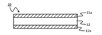
- FIG. 1A is a cross-sectional view schematically showing an example of a light selective transmission type glass.
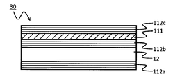
- FIG. 1B is a cross-sectional view schematically showing another example of the light selective transmission glass.
- FIG. 1C is a cross-sectional view schematically illustrating another example of the light selective transmission glass.
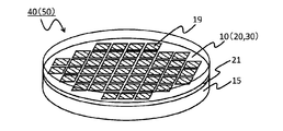
- FIG. 2 is a perspective view schematically showing an example of a laminated substrate.
- FIG. 3A is an enlarged cross-sectional view schematically showing an example of a laminated substrate.
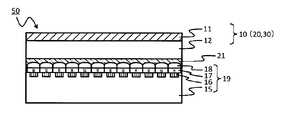
- FIG. 3B is an enlarged view of a cross section schematically showing another example of the laminated substrate.
- FIG. 4 is a graph (incident angle: 0 °) showing the spectral transmittance of a reflective layer made of a dielectric multilayer film.
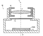
- FIG. 5 is a cross-sectional view schematically showing a main part of an example of a camera module.
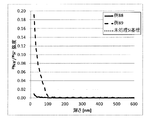
- FIG. 6 is a diagram showing SIMS measurement results representing the influence of the content of alkali metal oxide.
- the light selective transmission glass which is an embodiment of the present invention will be described with reference to FIGS. 1A to 1C.
- the use of the light selective transmission glass according to an embodiment of the present invention is not particularly limited.
- a near-infrared cut filter that blocks near infrared light and selectively transmits visible light, and blocks visible light and transmits near infrared light.
- a color filter that selectively transmits at least one selected from the group of visible light in the blue wavelength range, visible light in the red wavelength range, and visible light in the green wavelength range.
- FIG. 1A shows a light selective transmission type glass 10 having a light selective transmission layer 11 on one side of a parallel flat glass substrate 12.
- the glass substrate 12 is made of a glass material that is transparent to at least visible light having a wavelength of 380 nm to 780 nm. Furthermore, the surface of the glass substrate 12 only needs to have a surface flatness that can suppress generation of scattered light and transmission wavefront aberration that cause resolution degradation of the solid-state imaging device, and both sides are mirror-finished. May be.
- the glass substrate 12 has an average coefficient of thermal expansion ⁇ 50/100 at 50 ° C. to 100 ° C. of 2.70 ppm / ° C. to 3.20 ppm / ° C.
- ⁇ 50/100 is preferably 2.80 ppm / ° C. or more, more preferably 2.90 ppm / ° C. or more, further preferably 2.91 ppm / ° C. or more, and particularly preferably 2.92 ppm / ° C. or more.
- ⁇ 50/100 is preferably 3.10 ppm / ° C. or less, more preferably 3.00 ppm / ° C. or less, further preferably 2.96 ppm / ° C. or less, and particularly preferably 2.94 ppm / ° C. or less.
- ⁇ 50/100 is in the above range, so that the difference in thermal expansion coefficient between the glass substrate and the silicon substrate is small, so that the silicon substrate and the glass are bonded in the heat treatment step for bonding the silicon substrate and the glass substrate while ensuring a process margin. Residual strain generated in the substrate can be reduced.
- the average thermal expansion coefficient ⁇ 50 / 100 of 50 ° C. to 100 ° C. means that the temperature range for measuring the thermal expansion coefficient measured by the method defined in JIS R3102 (1995) is 50 ° C. to 100 ° C. It is a certain average thermal expansion coefficient.
- the glass substrate 12 has an average coefficient of thermal expansion ⁇ 200/300 at 200 ° C. to 300 ° C. of 3.45 ppm / ° C. to 3.95 ppm / ° C.
- ⁇ 200/300 is preferably 3.55 ppm / ° C. or more, more preferably 3.65 ppm / ° C. or more, particularly preferably 3.66 ppm / ° C. or more, and most preferably 3.68 ppm / ° C. or more.
- ⁇ 200/300 is preferably 3.85 ppm / ° C. or less, more preferably 3.75 ppm / ° C. or less, particularly preferably 3.73 ppm / ° C. or less, and most preferably 3.71 ppm / ° C. or less.
- ⁇ 200/300 is in the above range, a process margin when the glass substrate is bonded to the silicon substrate is secured, and defects such as residual strain due to a difference in thermal expansion coefficient from the silicon substrate are significantly reduced. Can be suppressed.
- ⁇ 200/300 is 3.55 ppm / ° C. to 3.85 ppm / ° C., the difference in thermal expansion coefficient from the silicon substrate is sufficiently small, so that defects caused by the difference in thermal expansion coefficient are further suppressed. can do.
- the average thermal expansion coefficient ⁇ 200/300 of 200 ° C. to 300 ° C. means that the temperature range for measuring the thermal expansion coefficient measured by the method defined in JIS R3102 (1995) is 200 ° C. to 300 ° C. Is an average coefficient of thermal expansion.
- the glass substrate 12 has a value ⁇ 200/300 / ⁇ 50/100 obtained by dividing the average thermal expansion coefficient ⁇ 200/300 at 200 ° C. to 300 ° C. by the average thermal expansion coefficient ⁇ 50/100 at 50 ° C. to 100 ° C. 1.20 to 1.30. If it is the above-mentioned range, since the difference of a thermal expansion coefficient with a silicon substrate is small, the residual distortion which generate
- ⁇ 200/300 / ⁇ 50/100 is preferably 1.24 to 1.27.
- the glass substrate 12 has an alkali metal oxide content of 0% to 0.1%.
- the alkali metal oxide is Li 2 O, Na 2 O, K 2 O, or the like.
- the content of the alkali metal oxide is preferably 0.05% or less, more preferably 0.02% or less, and still more preferably substantially not contained.
- substantially free of alkali metal oxide means that it does not contain alkali metal oxide at all, or may contain alkali metal oxide as an impurity inevitably mixed in production. .
- the glass substrate 12 preferably has the following composition. SiO 2 : 50% to 75%, Al 2 O 3 : 6% to 16%, B 2 O 3 : 0% to 15%, MgO: 0% to 15%, CaO: 0% to 13%, SrO: 0% to 11% BaO: 0% to 9.5%
- SiO 2 is a component that forms a glass skeleton.
- the content of SiO 2 is preferably 60% or more, and more preferably 64% or more.
- the content of SiO 2 is preferably 70% or less, more preferably 68%.
- the content of Al 2 O 3 is preferably 8% or more, and more preferably 11% or more.
- the content of Al 2 O 3 is preferably 14% or less.
- B 2 O 3 is not an essential component, by containing it, the viscosity at the time of melting the glass does not become too high, the meltability becomes good, and devitrification becomes difficult. If the content of B 2 O 3 is 15% or less, the glass transition temperature can be increased and the Young's modulus is increased.
- the content of B 2 O 3 is more preferably 3% or more. Further, the content of B 2 O 3 is preferably 12% or less, more preferably 6%.
- MgO is not an essential component, but when it is contained, the viscosity at the time of melting the glass does not become too high, the meltability is improved, the weather resistance is improved, and the Young's modulus is increased. When the content of MgO is 15% or less, devitrification is difficult.
- the MgO content is preferably 4% or more, and more preferably 6% or more. Further, the content of MgO is preferably 10% or less, more preferably 9.5% or less, and further preferably 9% or less.
- CaO is not an essential component, but by containing CaO, the viscosity at the time of melting the glass does not become too high, the meltability is improved, and the weather resistance is improved. If the content of CaO is 13% or less, devitrification becomes difficult.
- the CaO content is preferably 4% or more. Further, the CaO content is preferably 10% or less, and more preferably 8% or less.
- SrO is not an essential component, but by containing SrO, the viscosity at the time of melting the glass does not become too high, the meltability is improved, and the weather resistance is improved.
- the content of SrO is preferably 0.5% or more.
- the SrO content is preferably 8% or less, more preferably 3% or less.
- BaO is not an essential component, but when it is contained, the viscosity at the time of melting the glass does not become too high, the meltability is improved, and the weather resistance is improved. If the content of BaO is 9.5% or less, devitrification becomes difficult.
- the content of BaO is preferably 3% or less, and more preferably 2% or less.
- the glass substrate 12 preferably has a total content of CaO, SrO, and BaO of 7% or more. If the total content of CaO, SrO, and BaO is 7% or more, devitrification becomes difficult.
- the total content of CaO, SrO, and BaO is more preferably 7.5% or more, and even more preferably 8.0% or more.
- the glass substrate 12 preferably has (Al 2 O 3 content) ⁇ (MgO content). If (Al 2 O 3 content) ⁇ (MgO content), it is easy to match the average thermal expansion coefficient of the glass substrate to the average thermal expansion coefficient of the silicon substrate, and in the heat treatment step of bonding the silicon substrate and the glass substrate together. Residual strain generated in the silicon substrate and the glass substrate is small.
- the glass substrate 12 preferably has a devitrification viscosity ( ⁇ TL ) of 10 3.8 d ⁇ Pa ⁇ s or more. If the devitrification viscosity is 10 3.8 d ⁇ Pa ⁇ s or more, molding can be performed stably.
- the devitrification viscosity is more preferably 10 4.0 d ⁇ Pa ⁇ s or more, and further preferably 10 4.2 d ⁇ Pa ⁇ s or more.
- the content of Fe 2 O 3 is preferably 200 ppm or less.
- the content of Fe 2 O 3 is more preferably 150 ppm or less, further preferably 100 ppm or less, and particularly preferably 50 ppm or less.
- the glass substrate 12 may contain Fe 2 O 3 in excess of 200 ppm and 1000 ppm or less in terms of oxide-based mass parts per million. preferable. If exceeding the content 200ppm of Fe 2 O 3, it is possible to increase the thermal conductivity of the glass substrate, and good meltability. If the content of Fe 2 O 3 is 1000 ppm or less, the absorption of visible light does not become too strong.
- the content of Fe 2 O 3 is more preferably 300 ppm or more, further preferably 400 ppm or more, and particularly preferably 500 ppm or more.
- the content of Fe 2 O 3 is more preferably 800 ppm or less, further preferably 700 ppm or less, and particularly preferably 600 ppm or less.
- the glass substrate 12 may contain, for example, SnO 2 , SO 3 , Cl, and F as a fining agent.
- the glass substrate 12 is formed of, for example, ZnO, Li 2 O, WO 3 , Nb 2 O 5 , V for improving weather resistance, solubility, devitrification, ultraviolet shielding, infrared shielding, ultraviolet transmission, infrared transmission, and the like.
- 2 O 5 , Bi 2 O 3 , MoO 3 , P 2 O 5 , Ga 2 O 3 , I 2 O 5 , In 2 O 5 , Ge 2 O 5 and the like may be contained.
- the glass substrate 12 may contain 2% or less in total of ZrO 2 , Y 2 O 3 , La 2 O 3 , TiO 2 , SnO 2 in the glass in order to improve the chemical durability of the glass. Is contained at 1% or less, more preferably 0.5% or less. Among these, Y 2 O 3 , La 2 O 3 and TiO 2 contribute to the improvement of the Young's modulus of the glass.
- the glass substrate 12 preferably contains substantially no As 2 O 3 or Sb 2 O 3 in consideration of environmental load. In consideration of stable float forming, it is preferable that ZnO is not substantially contained.
- the glass substrate 12 has an average coefficient of thermal expansion ⁇ 100/200 at 100 ° C. to 200 ° C. of preferably 3.13 ppm / ° C. to 3.63 ppm / ° C., more preferably 3.23 ppm / ° C. to 3.53 ppm / ° C. If ⁇ 100/200 is within the above range, the difference in thermal expansion coefficient from the silicon substrate is small, so that a heat treatment process for bonding the silicon substrate and the glass substrate while securing a process margin is generated in the silicon substrate and the glass substrate. Residual stress can be reduced.
- ⁇ 100/200 is more preferably 3.33 ppm / ° C. or more, particularly preferably 3.34 ppm / ° C. or more, and most preferably 3.35 ppm / ° C. or more. Further, ⁇ 100/200 is more preferably 3.43 ppm / ° C. or less, particularly preferably 3.41 ppm / ° C. or less, and most preferably 3.38 ppm / ° C. or less.
- the average thermal expansion coefficient ⁇ 100/200 of 100 ° C. to 200 ° C. means that the temperature range for measuring the thermal expansion coefficient measured by the method defined in JIS R3102 (1995) is 100 ° C. to 200 ° C. Is an average coefficient of thermal expansion.
- the glass substrate 12 preferably has a Young's modulus of 80 GPa or more. If Young's modulus is 80 GPa or more, the curvature and the crack of the glass substrate which generate
- the Young's modulus is more preferably 81 GPa or more, further preferably 82 GPa or more, and particularly preferably 84 GPa or more.
- the Young's modulus is preferably 100 GPa or less. If the Young's modulus is 100 GPa or less, the glass can be prevented from becoming brittle, and chipping during cutting and dicing of the glass substrate can be suppressed.
- the Young's modulus is more preferably 90 GPa or less, and further preferably 87 GPa or less.
- the thickness of the glass substrate 12 is preferably 1.0 mm or less. If the thickness is 1.0 mm or less, the image sensor can be downsized. The thickness is more preferably 0.8 mm or less, further preferably 0.7 mm or less, and particularly preferably 0.5 mm or less.
- the thickness is preferably 0.1 mm or more. If the thickness is 0.1 mm or more, damage due to contact with a silicon substrate, peripheral members, or the like can be suppressed. In addition, the self-weight deflection of the light selective transmission glass can be suppressed.
- the thickness is more preferably 0.2 mm or more, and further preferably 0.3 mm or more.
- the glass substrate 12 preferably has an area of 0.01 m 2 or more. If the area is 0.01 m 2 or more, a large silicon substrate can be used, and a large number of image sensors can be produced. Area may also be 0.02 m 2 or more, may also be 0.03 m 2 or more, may also be 0.04 m 2 or more, may be 0.05 m 2 or more.
- the glass substrate 12 has ⁇ 200/300 of 3.45 ppm / ° C. to 3.95 ppm / ° C., and ⁇ 200/300 / ⁇ 50/100 of 1.20 to 1 Therefore, even if the area is 0.01 m 2 or more, the residual stress generated in the silicon substrate and the glass substrate is small in the heat treatment step for bonding the silicon substrate and the glass substrate.
- the area is preferably 0.1 m 2 or less. If the area is 0.1 m 2 or less, the light selective transmission glass can be easily handled, and damage due to contact with a silicon substrate, peripheral members, and the like can be suppressed. Area is more preferably 0.08 m 2 or less, more preferably 0.06 m 2 or less.
- the glass substrate 12 which is one Embodiment of this invention, a density of 2.60 g / cm ⁇ 3 > or less is preferable. If the density is 2.60 g / cm 3 or less, the light selective transmission glass is lightweight. Further, it is possible to reduce the deflection caused by the weight of the light selective transmission glass. Density is more preferably 2.55 g / cm 3 or less, more preferably 2.50 g / cm 3 or less.
- the density is preferably 2.20 g / cm 3 or more. If the density is 2.20 g / cm 3 or more, the Vickers hardness of the glass is increased, and the glass surface can be hardly damaged. Density is more preferably 2.30 g / cm 3 or more, more preferably 2.40 g / cm 3 or more, 2.45 g / cm 3 or more is particularly preferable.
- the glass substrate 12 which is one embodiment of the present invention preferably has a density of defects contained in the glass substrate of 1 piece / cm 2 or less.
- the defects included in the glass substrate are bubbles, scratches, metallic foreign matters such as platinum, unmelted raw materials, and the like existing on the surface or inside of the glass substrate, and have a size of 0.5 ⁇ m or more and 1 mm or less. If the defect is larger than 1 mm, it can be easily discriminated visually, and the removal of the substrate having the defect is easy. If the defect is smaller than 0.5 ⁇ m, the defect is sufficiently small, so that there is no possibility of affecting the characteristics of the device even when applied as a cover glass for a CMOS sensor or LCOS.
- the substrate having the defect can be excluded at the initial stage of the assembling process.
- the wafer level package since the laminated substrate is separated into pieces at the end of the assembly process, if there is a defect in the glass substrate, the glass substrate having the defect can be excluded at the end of the assembly process.
- the density of defects is more preferably 0.1 piece / cm 2 or less, and still more preferably 0.01 piece / cm 2 or less.
- the glass substrate has a non-uniform refractive index typified by striae, the photographed image or the projected image is distorted, and the quality of the photograph or video is degraded. Therefore, it is preferable that there is no non-uniform refractive index in the glass substrate.
- the refractive index difference is preferably within 10 ⁇ 4 , and more preferably within 10 ⁇ 5 .
- the shape of the glass substrate may be circular, elliptical or rectangular.
- the end of the glass substrate may have a notch, or when the glass substrate is circular, a part of the outer periphery of the glass substrate may be a straight line.
- the glass substrate 12 preferably has a glass transition point (Tg) of 700 ° C. or higher.
- Tg glass transition point
- the glass transition point (Tg) is more preferably 720 ° C. or higher, and further preferably 740 ° C. or higher.
- the glass substrate preferably has a virtual viscosity of 10 11.0 d ⁇ Pa ⁇ s to 10 14.1 d ⁇ Pa ⁇ s.
- the cooling rate after forming the glass plate is 1 ° C./min to 1200 ° C./min. It needs to be considerable.
- the average thermal expansion coefficient of the glass substrate is close to the average thermal expansion coefficient of the silicon substrate, and the silicon substrate and the glass substrate Residual stress generated in the silicon substrate and the glass substrate is small in the heat treatment step of bonding together.
- the virtual viscosity of the glass substrate is preferably 10 12.1 d ⁇ Pa ⁇ s to 10 13.1 d ⁇ Pa ⁇ s (equivalent to a cooling rate of 10 ° C. to 100 ° C./min).
- the virtual viscosity ( ⁇ ) of glass can be calculated by the following (formula 4) (GW Scherer, Relaxation in Glass and Compositions, Wiley, New York (1986), p. 159).
- the unit of ⁇ is d ⁇ Pa ⁇ s
- q is an assumed cooling rate
- the unit is ° C./s.
- the assumed cooling rate q is determined from the glass substrate by the following method.
- a plurality of small glass plate pieces are cut out from a single glass substrate having a thickness of 1 mm or less. For example, a 1 cm square piece is cut out as a glass plate piece.
- the cut glass plate pieces are each heat-treated and cooled at various cooling rates V, and the physical property values of the individual glass plate pieces are measured.
- the cooling start temperature is preferably a sufficiently high temperature that is not affected by the cooling rate. Typically, Tg + 50 ° C. to + 150 ° C. is preferable.
- a calibration curve A is prepared by taking the cooling rate (log 10 V) on the x-axis and taking the physical property values of the glass plate pieces subjected to the respective heat treatments on the y-axis. From the physical property values of the glass plate pieces not subjected to heat treatment, the assumed cooling rate q of the glass substrate is obtained by the prepared calibration curve A.
- the glass substrate 12 preferably has a temperature (T 2 ) at which the viscosity is 10 2 d ⁇ Pa ⁇ s, 1800 ° C. or lower.
- T 2 is more preferably 1750 ° C. or less, further preferably 1700 ° C. or less, and particularly preferably 1650 ° C. or less.
- the glass substrate 12 preferably has a temperature (T 4 ) at which the viscosity becomes 10 4 d ⁇ Pa ⁇ s, 1350 ° C. or lower.
- T 4 is more preferably 1300 ° C. or less, further preferably 1275 ° C. or less, and particularly preferably 1250 ° C. or less.
- the temperature (T 4 ) at which the viscosity is 10 4 d ⁇ Pa ⁇ s is 1100 ° C. or higher.
- the glass substrate 12 preferably has a devitrification temperature of 1325 ° C. or lower. 1300 degrees C or less is more preferable, 1275 degrees C or less is further more preferable, and 1250 degrees C or less is especially preferable.
- Glass devitrification temperature refers to putting crushed glass particles in a platinum dish, heat-treating them in an electric furnace controlled at a constant temperature for 17 hours, and observing crystals inside the glass by optical microscope observation after the heat treatment. It is an average value of the maximum temperature at which precipitation occurs and the minimum temperature at which crystals do not precipitate.
- the glass substrate 12 which is one embodiment of the present invention is 0.0177 ⁇ (SiO 2 content) ⁇ 0.0173 ⁇ (Al 2 O 3 content) + 0.0377 ⁇ (B 2 O 3 content) + 0.0771 ⁇ (MgO content) +0. 1543 ⁇ (CaO content) + 0.1808 ⁇ (SrO content) + 0.2082 ⁇ (BaO content) + 0.0344 ⁇ (12.3 + log 10 60-log 10 ⁇ ) is 2.70-3.
- the content of SiO 2, the content of Al 2 O 3 , the content of B 2 O 3 , the content of MgO, the content of CaO, the content of SrO, and the content of BaO were obtained.
- the content of each component contained in the glass, ⁇ is a virtual viscosity (unit: d ⁇ Pa ⁇ s).
- the glass substrate 12 has a weight reduction amount (hereinafter also referred to as HF weight reduction amount) with respect to a hydrofluoric acid aqueous solution (HF) of 0.05 (mg / cm 2 ) / min or more, 0.20. (Mg / cm 2 ) / min or less is preferable.
- HF weight reduction amount is the reduction amount per unit area and unit time ((mg / cm 2 ) / min) when the glass substrate is immersed in a 5% by mass hydrofluoric acid aqueous solution at 25 ° C.
- the glass substrate 12 according to an embodiment of the present invention is incorporated into a device as an optical filter after being bonded to a silicon substrate.
- HF weight loss can be used as an index of the slimming rate of the glass substrate.
- the amount of HF weight loss is 0.05 (mg / cm 2 ) / min or more, the productivity of the slimming process is improved, which is preferable. If the amount of HF weight loss is 0.20 (mg / cm 2 ) / min or less, defects such as non-uniform etching depth that occur on the glass substrate in the slimming process and the smoothness of the glass substrate surface are impaired. Can be prevented.
- the amount of HF weight reduction is more preferably 0.07 (mg / cm 2 ) / min or more, more preferably 0.09 (mg / cm 2 ) / min or more, and 0.11 (mg / cm 2 ) / min or more. Particularly preferred.
- the HF weight reduction amount is more preferably 0.18 (mg / cm 2 ) / min or less, further preferably 0.16 (mg / cm 2 ) / min or less, and 0.14 (mg / cm 2 ) / min. Minutes or less are particularly preferred.
- the light selective transmission glass that is one embodiment of the present invention can be applied as a display device for projection use, for example, an optical filter of LCOS.
- the photoelastic constant of the glass substrate is high, the glass substrate will have birefringence due to stress generated during the device packaging process or during device use. As a result, color change occurs in the light incident on the device, which may cause image quality defects such as color unevenness.
- the glass substrate 12 preferably has a photoelastic constant of 31 nm / (MPa ⁇ cm) or less, more preferably 30.5 nm / (MPa ⁇ cm) or less. 30 nm / (MPa ⁇ cm) or less, more preferably 29.5 nm / (MPa ⁇ cm) or less.
- alpha-ray emission of the glass substrate is preferably not more than 0.5C / cm 2 ⁇ h, more preferably not more than 0.3C / cm 2 ⁇ h, the following are particularly preferred 0.1C / cm 2 ⁇ h, 0 .05 C / cm 2 ⁇ h or less is most preferable.
- the unit C means the count number.
- light selective transmission type glass which is an embodiment of the present invention is applied to a cover glass of a solid-state imaging device.
- ⁇ -rays generated from the glass substrate are incident on the solid-state imaging device, hole-electron pairs are induced by the energy of the ⁇ -rays, and this causes software to generate bright spots and white spots instantaneously. An error may occur. Therefore, such a problem can be easily prevented by using a glass substrate with a small amount of ⁇ -ray emission. If a high-purity raw material with a low content of radioactive isotopes and a small amount of ⁇ -ray emission is used as a raw material for the glass substrate, the amount of ⁇ -ray emission can be reduced.
- the ⁇ -ray emission amount can be effectively reduced. Further, the “ ⁇ -ray emission amount” can be measured by a gas flow proportional counter measuring device or the like.
- a melting step of obtaining a molten glass by heating a glass raw material a clarification step of removing bubbles from the molten glass, a forming step of obtaining a glass ribbon by forming the molten glass into a plate shape
- a slow cooling step of slowly cooling the glass ribbon to room temperature a melting step of obtaining a molten glass by heating a glass raw material, a clarification step of removing bubbles from the molten glass, a forming step of obtaining a glass ribbon by forming the molten glass into a plate shape.
- raw materials are prepared so as to have a composition of the obtained glass plate, and the raw materials are continuously charged into a melting furnace, and preferably heated to about 1450 ° C. to 1650 ° C. to obtain molten glass.
- halides such as oxides, carbonates, nitrates, hydroxides and chlorides can also be used.
- halides such as oxides, carbonates, nitrates, hydroxides and chlorides.
- strontium nitrate As the nitrate, strontium nitrate, barium nitrate, magnesium nitrate, calcium nitrate and the like can be used. More preferably, strontium nitrate is used. From raw materials with a large particle size of several hundred microns that do not cause undissolved raw material particle size, to materials with a small particle size of about several microns that do not scatter during transportation of the raw material and do not agglomerate as secondary particles it can. The use of granules is also possible. In order to prevent scattering of the raw material, the water content of the raw material can be appropriately adjusted. The solubility conditions such as ⁇ -OH, Fe oxidation-reduction degree or redox [Fe 2+ / (Fe 2+ + Fe 3+ )] can be appropriately adjusted and used.
- the clarification step is a step of removing bubbles from the molten glass obtained in the melting step.
- a defoaming method using reduced pressure may be applied.
- the glass substrate can use SO 3 or SnO 2 as a fining agent.
- the SO 3 source is preferably a sulfate of at least one element selected from Al, Mg, Ca, Sr and Ba, more preferably an alkaline earth metal sulfate, and among them, CaSO 4 .2H 2 O, SrSO 4 and BaSO 4 are particularly preferable because they have a remarkable effect of increasing bubbles.
- Halogens such as Cl and F are preferably used as the clarifying agent in the defoaming method using reduced pressure.
- Cl source a chloride of at least one element selected from Al, Mg, Ca, Sr and Ba is preferable, and a chloride of an alkaline earth metal is more preferable.
- SrCl 2 .6H 2 O, and BaCl 2 ⁇ 2H 2 O is, for remarkably acts to increase the foam, and a small deliquescent, particularly preferred.
- the F source a fluoride of at least one element selected from Al, Mg, Ca, Sr and Ba is preferable, and a fluoride of an alkaline earth metal is more preferable.
- CaF 2 is the solubility of the glass raw material. The effect of increasing the value is remarkably more preferable.
- the forming step is a step of obtaining a glass ribbon by forming the molten glass from which bubbles have been removed in the clarification step into a plate shape.
- a float method is used in which molten glass is poured over molten metal to form a glass ribbon.
- the slow cooling step is a step of gradually cooling the glass ribbon obtained in the molding step to a room temperature state.
- the glass ribbon is kept at room temperature so that the average cooling rate from the temperature at which the viscosity becomes 10 13 d ⁇ Pa ⁇ s to the temperature at 10 14.5 d ⁇ Pa ⁇ s becomes R. Allow to cool slowly.
- a glass substrate is obtained after cutting the slowly cooled glass ribbon.
- the composition of the obtained glass substrate and the average cooling rate R (unit: ° C./min) of the glass ribbon in the slow cooling process satisfy the following conditions (1) to (4).
- Condition (1) 0.0177 ⁇ (SiO 2 content) ⁇ 0.0173 ⁇ (Al 2 O 3 content) + 0.0377 ⁇ (B 2 O 3 content) + 0.0771 ⁇ (MgO content) +0. 1543 ⁇ (CaO content) + 0.1808 ⁇ (SrO content) + 0.2082 ⁇ (BaO content) + 0.0344 ⁇ log 10 R is 2.80 to 3.10
- the content of SiO 2, the content of Al 2 O 3 , the content of B 2 O 3 , the content of MgO, the content of CaO, the content of SrO, and the content of BaO were obtained. It is content of each component contained in glass.
- the content of alkali metal oxide is 0.1% or less, so that in the heat treatment step of bonding the silicon substrate and the glass substrate, alkali ions are present. Difficult to diffuse into silicon substrate.
- the average coefficient of thermal expansion ⁇ 50/100 at 50 ° C. to 100 ° C. is 2.70 ppm / ° C. to 3.20 ppm / ° C.
- the average coefficient of thermal expansion ⁇ 200/300 at 200 ° C. to 300 ° C. is 3. 45 ppm / ° C. to 3.95 ppm / ° C. Value obtained by dividing the average thermal expansion coefficient ⁇ 200/300 from 200 ° C. to 300 ° C.
- the present invention is not limited to the above embodiment.
- the present invention includes modifications and improvements as long as the object of the present invention can be achieved.
- the molten glass when the glass substrate according to the present invention is manufactured, the molten glass may be formed into a plate shape by applying a fusion method or a press molding method in the molding step.
- the glass substrate which is one Embodiment of this invention
- a platinum crucible in the melting step, raw materials are prepared so that the composition of the obtained glass substrate is obtained, the platinum crucible containing the raw materials is put into an electric furnace, and preferably heated to about 1450 ° C. to 1650 ° C. Then, a platinum stirrer is inserted and stirred for 1 to 3 hours to obtain molten glass.
- molten glass is poured into, for example, a carbon plate to form a plate.
- the plate-like glass is gradually cooled to room temperature, and after cutting, a glass substrate is obtained.
- the glass substrate obtained by cutting may be gradually cooled to room temperature after being heated to, for example, about Tg + 50 ° C. In this way, the virtual viscosity ⁇ can be adjusted.
- the light selective transmission layer 11 is selected from the group of near infrared rays, visible rays, visible rays in the blue wavelength range, visible rays in the red wavelength range, and visible rays in the green wavelength range among the near infrared rays and visible rays.
- a layer selectively transmitting at least one of the layers.
- the light selective transmission layer 11 is preferably a layer that selectively transmits three or less selected from the above group.
- the light selective transmission layer 11 includes (1) near infrared rays, (2) visible rays, (3) visible rays in the blue wavelength region, (4) visible rays in the red wavelength region, and (5) green. (6) Near infrared and blue wavelength visible light, (7) Near infrared, blue wavelength visible light and red wavelength visible light, (8) Near infrared, blue Visible light in the wavelength range and visible light in the green wavelength range, (9) visible light in the near infrared and red wavelength range, (10) visible light in the near infrared, red wavelength range and green wavelength range.
- the wavelengths of each light are near infrared: 780 nm to 1200 nm, visible light: 380 nm to 780 nm, visible light in the red wavelength region: 600 nm to 780 nm, visible light in the green wavelength region: 500 nm to 600 nm, and blue wavelength. Visible light in the region: 380 nm to 500 nm.
- “selectively transmit” means that the external transmittance is 80% or more at maximum in each wavelength range.
- the external transmittance is a transmittance of transmitted light other than a component that is not transmitted by reflection or absorption in incident light, and can be measured using a commercially available double beam type near-infrared visible spectrophotometer or the like. Further, the external transmittance of a fine region can be measured using a microspectrophotometer attached with a microscope.
- the light selective transmission layer 11 is preferably composed of an absorption layer and / or a reflection layer. In the case of a color filter application, it is preferably composed of an absorption layer.
- the absorbing layer may be formed of, for example, a layer containing an absorbing dye that absorbs light having a wavelength that is not desired to be transmitted and a transparent resin. A plurality of absorbing dyes may be contained.
- the reflective layer may be formed of, for example, a dielectric multilayer film in which two or more kinds of dielectric thin films having different refractive indexes are laminated.
- the light having a wavelength that is not desired to be transmitted is reflected by the reflection action of the reflection layer, specifically, the interference action of the dielectric multilayer film.
- the reflective layer can give sharper light selective transparency, which is difficult to achieve with the absorption layer. For example, in the case of a near-infrared cut filter application, the visible light transmittance can be increased by configuring the light selective transmission layer 11 with a reflection layer as compared with the case with an absorption layer.
- the light selective transmission layer 11 may be divided into a rectangle or a polygon.
- the light absorption characteristics of the divided light selective transmission layers 11 may be different to correspond to, for example, red, green, and blue light.
- the light selective transmission layer 11 may be divided by a light shielding part such as a black matrix.
- FIG. 1B shows a light selective transmission type glass 20 in which light selective transmission layers 11 a and 11 b are formed on both surfaces of a glass substrate 12.
- the light selective transmission characteristics of the light selective transmission layers 11a and 11b may be the same or different.
- the light selective transmission glass may have a reflection layer made of a dielectric multilayer film in addition to the absorption layer.
- a reflection layer made of a dielectric multilayer film in addition to the absorption layer.
- near-ultraviolet light and near-infrared light that cannot be sufficiently blocked only by the absorption layer 111 can be blocked by the reflection action.
- near-ultraviolet rays and visible rays can be blocked in the case of near-infrared transmission filter applications.
- FIG. 1C shows a light selective transmission type glass 30 in which reflection layers 112a, 112b, and 112c are formed in addition to the light selective transmission layer composed of the absorption layer 111.
- the reflection layers 112a and 112b are provided on one surface or / and both surfaces of the glass substrate 12, or the surface of the light selective transmission layer including the absorption layer 111 is provided with a reflection layer 112c. Also good.
- the light selective transmission type glass 30 may include an antireflection film, and may be subjected to a surface treatment with a silane coupling agent for improving the adhesion and reliability of the light selective transmission layer, or a dielectric film. May be provided. Since one of 112a and 112c located on the surface of the light selective transmission type glass 30 is bonded to the silicon substrate by an adhesive, it may be designed in consideration of the refractive index of the adhesive.
- the light selective transmission type glass 30 is bonded to a silicon substrate on which a solid-state image sensor is formed, and is disposed at a position close to the pixel. For this reason, if there are foreign matters or minute defects in the reflective layers 112a, 112b, and 112c, they can directly become pixel defects, and therefore the allowable level of the size and the number of occurrences is stricter than the reflective layer in the non-junction type optical filter. There are many cases. Therefore, it is preferable that the light selective transmission glass 30 includes the reflective layers 112a, 112b, and 112c according to the quality level.
- the light selective transmission type glass which is an embodiment of the present invention includes a function of a cover glass for protecting the solid-state imaging device, it is possible to expect a reduction in size and thickness of the imaging device.
- the glass substrate contains an ⁇ -ray emitting element (radioisotope) as an impurity, it may emit a ray and cause a soft error in the solid-state imaging device. It is recommended to use a glass material with a small amount of high purity.
- the content of U and Th among the ⁇ -ray emitting elements is preferably 20 ppb or less, and more preferably 5 ppb or less.
- the light selective transmission type glass may be provided with a film that shields ⁇ rays on one side close to the solid-state imaging device.
- the absorbing layer constituting the light selective transmission layer 11 is a layer containing a near-infrared absorbing dye (A) (hereinafter also referred to as “dye (A)”) and a transparent resin (B) as an absorbing dye. Specifically, it is a layer in which the pigment (A) is uniformly dissolved or dispersed in the transparent resin (B).
- the light selective transmission layer 11 may further contain a near-ultraviolet absorbing dye (U) (hereinafter also referred to as “dye (U)”).
- the light selective transmission layer 11 also includes a dye (U).
- the configuration is not limited to this.
- the light selective transmission layer 11 contains the dye (A) and the transparent resin (B) and does not contain the dye (U)
- a configuration may be provided in which a near-ultraviolet absorbing layer not shown in FIGS. 1A to 1C is separately provided.
- the near-ultraviolet absorbing layer may contain a pigment (U) and a transparent resin and be provided as an independent layer.
- the near-ultraviolet absorbing layer may be provided on the light selective transmission layer 11 side of both main surfaces of the glass substrate 12, or may be provided on the side facing the light selective transmission layer 11 side, and the positional relationship thereof.
- the light selective transmission glass that is one embodiment of the present invention has the same optical characteristics as the configuration in which the light selective transmission layer 11 further contains a dye (U). Optical properties are obtained.
- the light selective transmission layer 11 contains the dye (A), the transparent resin (B), and further the dye (U)
- a near-ultraviolet absorbing layer containing the dye (U) and the transparent resin (B) is separately provided. It may be provided.
- the light selective transmission glass according to an embodiment of the present invention will be described as a configuration in which the light selective transmission layer 11 contains the dye (U) when it contains the dye (U).
- the dye (A) is not particularly limited as long as it has the ability to transmit light in the visible light region (wavelength 380 nm to 780 nm) and absorb light in the near infrared region (wavelength 780 nm to 1200 nm).
- the dye in the present invention may be a pigment, that is, a state in which molecules are aggregated.
- Examples of the dye (A) include cyanine compounds, phthalocyanine compounds, naphthalocyanine compounds, dithiol metal complex compounds, diimonium compounds, polymethine compounds, phthalide compounds, naphthoquinone compounds, anthraquinone compounds, and indophenol compounds. Examples include compounds and squarylium compounds.
- the near-ultraviolet absorbing dye (U) is not particularly limited as long as it has an ability to absorb light having a wavelength of 430 nm or less.
- the dye (U) include oxazole, merocyanine, cyanine, naphthalimide, oxadiazole, oxazine, oxazolidine, naphthalic acid, styryl, anthracene, cyclic carbonyl, and triazole.
- the pigment (A) is preferably contained in the light selective transmission layer 11 in an amount of 0.1 to 30 parts by mass, preferably 0.5 to 25 parts by mass with respect to 100 parts by mass of the transparent resin (B). More preferably, the content is 1 to 20 parts by mass.
- the content of the dye (U) in the light selective transmission layer 11 is preferably 0.01 to 30 parts by mass, and 0.05 to 25 parts by mass with respect to 100 parts by mass of the transparent resin (B). More preferably, the content is 0.1 to 20 parts by mass.
- the light selective transmission layer 11 includes, in addition to the dye (A), the transparent resin (B), and the optional dye (U), a light absorber, a color tone correction dye, a near ultraviolet absorber, a leveling agent, an antistatic agent, You may contain a heat stabilizer, a light stabilizer, antioxidant, a dispersing agent, a flame retardant, a lubricant, a plasticizer, etc.
- the component added to the coating liquid used when forming the light selective transmission layer 11 mentioned later for example, the component derived from a silane coupling agent, a heat
- the content of these other optional components in the absorbent layer is preferably 15 parts by mass or less with respect to 100 parts by mass of the transparent resin (B).
- the film thickness of the light selective transmission layer 11 is preferably 0.1 ⁇ m to 10 ⁇ m. If the film thickness is less than 0.1 ⁇ m, the light absorption ability may not be sufficiently exhibited. On the other hand, if the film thickness exceeds 10 ⁇ m, the flatness of the film is lowered, and there is a possibility that the absorption rate varies.
- the film thickness is more preferably 1 ⁇ m to 10 ⁇ m. If it exists in this range, sufficient light absorptivity and flatness of a film thickness can be compatible. Even when a near ultraviolet absorbing layer is separately provided, the film thickness of the near ultraviolet absorbing layer only needs to satisfy the above range.
- the light selective transmission layer 11 is, for example, a coating prepared by dispersing and dissolving a dye (A), a transparent resin (B), or a raw material component of the transparent resin (B), and optionally a dye (U) in a solvent.
- the liquid can be manufactured by coating on the glass substrate 12, drying, and further curing as necessary. By forming the light selective transmission layer 11 by such a method, it can be uniformly produced with a desired film thickness.
- the coating liquid contains the optional component.
- the light selective transmission layer 11 is formed on the glass substrate 12 by applying the coating liquid onto the glass substrate 12 and then drying it.
- the coating solution contains the raw material component of the transparent resin (B)
- a curing treatment is further performed.
- the reaction is thermosetting, drying and curing can be performed simultaneously.
- a curing process is provided separately from the drying.
- the transparent resin (B) is specifically acrylic resin, epoxy resin, ene thiol resin, polycarbonate resin, polyether resin, polyarylate resin, polysulfone resin, polyethersulfone resin, polyparaphenylene resin, polyarylene ether.
- Examples include phosphine oxide resins, polyimide resins, polyamideimide resins, polyolefin resins, cyclic olefin resins, and polyester resins.
- 1 type may be used individually from these resin, and 2 or more types may be mixed and used for it.
- the light selective transmission layer 11 includes a reflection layer that reflects near infrared rays and transmits visible light
- the reflection layer constituting the light selective transmission layer 11 is formed of a dielectric multilayer film as described above.
- it is formed of a dielectric multilayer film having a high refractive index layer having a refractive index of 2.0 or more and a low refractive index layer having a refractive index of 1.7 or less.
- the high refractive index layer can be selected from TiO 2 , Nb 2 O 5 , Ta 2 O 5 , or a composite oxide thereof.
- the low refractive index layer can be selected from SiO 2 , MgF 2 , Al 2 O 3 , or a composite oxide thereof.
- the light selective transmission layer 11 may be provided on both surfaces of the glass substrate as shown in FIG. 1B. Since the light selective transmission layer 11 made of a dielectric multilayer film is formed by laminating several tens of optical thin films on a glass substrate, the glass substrate may be warped due to film stress particularly when the glass substrate is thin. However, warpage can be alleviated by forming a dielectric multilayer film on both surfaces of the glass substrate so that the film stresses on both surfaces of the glass substrate are substantially equal.
- a high refractive index layer and a low refractive index layer are alternately and repeatedly laminated with the same optical film thickness. It is common to have repeated alternating layers. Repeated alternating layers are represented as (1H, 1L) S.
- the wavelength near the center of the wavelength to be cut is designated as the design wavelength ⁇
- S is the number of repetitions called the number of stacks, and indicates that the configuration in parentheses is repeated periodically.
- the specific wavelength to be cut is determined by this repeated alternating layer.
- S the falling characteristic (steepness) that changes to absorption-transmission becomes steep.
- the value of S is selected from a range of about 2 to 7, and it is preferable to stack the layers by gradually changing the thickness of the repeated layers of the normal basic design.
- the substrate is expressed as
- TiO 2 or the like is used for the high refractive index layer, the design is often performed by adding SiO 2 having better environmental resistance characteristics to the outermost layer rather than ending the outermost layer with the high refractive index layer. Since the characteristics of the layer in contact with the glass substrate may deteriorate due to the reaction of TiO 2 with the glass substrate, chemically stable SiO 2 may be added to the first layer.
- the design of the light selective transmission layer 11 using such a multilayer film can be theoretically performed using commercially available software (reference: OPTRONICS magazine 1999 No. 5 p.175-190).
- ⁇ is 755 nm
- the following stacked structure of 40 layers can be exemplified. 1.17H, 1.13L, (0.95H, 0.99L) 4, (1.05H, 1.1L) 4, (1.18H, 1.22L) 2, (1.25H, 1.28L) 3, (1.33H, 1.34L) 5, 1.16H, 0.59L.
- a physical film forming method is generally used, and a normal vacuum deposition method is also possible.
- the present invention provides a laminated substrate in which a silicon substrate and a light selective transmission glass are bonded.
- a laminated substrate is provided in which a silicon substrate on which a plurality of solid-state imaging elements for manufacturing a camera module is formed and light selective transmission glass are bonded.
- FIG. 2 shows an example of a laminated substrate 40 (50) in which a light selective transmission type glass substrate 10 (20, 30) and a silicon substrate 15 on which a plurality of solid-state image sensors 19 are formed are bonded according to an embodiment of the present invention.
- 3A and 3B are enlarged views of the periphery of the solid-state imaging device 19 of the laminated substrate 40 (50) in which the light selective transmission glass 10 (20, 30) according to an embodiment of the present invention is integrated with the solid-state imaging device 19. It is a cross-sectional schematic diagram.
- the solid-state imaging device 19 is formed by forming an Si semiconductor (CMOS, CCD) photodetector array 16 on one surface of a silicon substrate 15 and an RGB mosaic color filter 17 and a resin microlens 18 for each pixel.
- CMOS, CCD Si semiconductor
- the silicon substrate 15 and the light selective transmission glass 10 (20, 30) are integrated through an adhesive 21 to form a laminated substrate 40 (50).
- the laminated substrate 50 in FIG. 3B has a configuration in which the light selective transmission layer 11 faces the air side and is integrated on the side facing the light selective transmission layer 11 via an adhesive 21.
- the adhesive 21 may be any material that is transparent to visible light.
- the arrangement of the light selective transmission layer 11 may be on the solid-state imaging device 19 side (FIG. 3A) or on the air side (FIG. 3B). Since the absorption layer is softer than the glass substrate, the surface is easily scratched. Therefore, when the light selective transmission layer 11 is formed of a single layer, if it is disposed on the bonding surface side of the solid-state imaging device 19, subsequent manufacturing is performed. Scratches hardly occur in the process.
- the laminated substrate 50 is configured to be obtained also in the step of forming the light selective transmission layer 11 on the surface of the glass substrate 12 after bonding the glass substrate 12 to the silicon substrate 15. That is, the laminated substrate 50 can obtain the same configuration even if the order of the formation of the light selective transmission layer 11 and the joining of the glass substrate and the solid-state imaging device are not limited.
- the resin microlens 18 has a convex lens function that collects incident light on the light receiving surface of the photodetector array 16. Therefore, it is preferable that the refractive index n ML of the transparent resin used for the resin microlens 18 and the refractive index n G of the adhesive 21 satisfy n ML > n G , and the refractive index difference (n ML ⁇ n G ) is as large as possible. Specifically, n ML ⁇ 1.8 is preferable, and n ML ⁇ 1.9 is more preferable. Further, n G ⁇ 1.5 is preferable, and n G ⁇ 1.45 is more preferable.
- the adhesive 21 may be either an ultraviolet curable type or a thermosetting type, but an ultraviolet curable type is preferable in that an adhesive strength can be obtained in a short time.
- the ultraviolet curable adhesive provides sufficient adhesive strength between the resin microlens 18 surface and the glass surface or the absorption layer surface of the light selective transmission glass 10 (20, 30).
- Adhesive 21 has a polymerization shrinkage rate of 3% or less upon curing, is less susceptible to misalignment and lowering of adhesive strength due to ambient environmental conditions such as high temperature and high quality, and rapid temperature changes, and has a low halogen content. Those with less outgassing due to later unreacted components are preferred.
- Bonding with the adhesive 21 is performed by applying a pre-curing adhesive to the light selective transmission glass 10 (20, 30), and having a uniform film thickness of 10 ⁇ m or less between the light selective transmission glass and the solid-state imaging device 19.
- the laminated substrate 40 (50) is obtained.
- the adhesive 21 may be irradiated with ultraviolet rays from the light selective transmission glass 10 (20, 30) side to be polymerized and cured.
- the entire laminated substrate 50 is preferably heated and polymerized.
- the light selective transmission layer 11 does not transmit ultraviolet rays in the curing process of the adhesive 21 or is altered by heat treatment, after the glass substrate 12 and the solid-state imaging device 19 are bonded, the light selective transmission layer 11 is formed on the surface of the glass substrate 12.
- the light selective transmission layer 11 may be formed.
- the voltage application of the solid-state imaging device 19 and the electric wiring for extracting the electric signal are omitted.
- the electrical wiring is arranged on the side of the silicon substrate 15 facing the photodetector array 16, and the through electrode of the silicon substrate 15 An example in which the electrode is drawn out to the back surface of the solid-state imaging device by a technique such as the above.
- FIG. 5 is a cross-sectional view schematically showing a main part of the solid-state imaging device 60.
- the solid-state imaging device 19 to which the light selective transmission glass 10 (20) is bonded, the reflective layer 112 on the front surface, and the imaging It has the lens 31 and the housing
- the imaging lens 31 is fixed by a lens unit 32 provided inside the housing 33.
- the reflective layer 112 has a dielectric multilayer film on one side or both sides of the transparent substrate, and is disposed in the optical path between the light incident side of the lens unit 32 and the solid-state imaging device 19.
- FIG. 5 shows an example in which the reflective layer 112 is disposed between the lens unit 32 and the light selective transmission glass 10 (20).
- the present invention is not limited to this example, and the dielectric of the reflective layer 112 is shown.
- a configuration in which a body multilayer film is formed on the surface of the imaging lens 31 may be used.
- the laminated substrate 40 (50) can incorporate the optical filter function into the solid-state imaging device 19 at the wafer level, the productivity can be improved and the characteristics can be stabilized. Further, the conventional optical filter function is integrated in the solid-state image sensor 19 and the imaging lens 31, and the assembly adjustment of the camera module is simplified by reducing the number of optical filter components, and the solid-state imaging device can be miniaturized.
- the laminated substrate according to an embodiment of the present invention is formed by laminating a light selective transmission type glass and a silicon substrate, and has an average thermal expansion coefficient ⁇ 50/100 of 50 ° C. to 100 ° C. of the glass substrate,
- ⁇ 50/100 is more preferably at least ⁇ 0.15 ppm / ° C., further preferably at least ⁇ 0.10 ppm / ° C., particularly preferably at least ⁇ 0.05 ppm / ° C., and most preferably at least ⁇ 0.03 ppm / ° C.
- ⁇ 50/100 is more preferably 0.15 ppm / ° C. or less, further preferably 0.10 ppm / ° C. or less, particularly preferably 0.05 ppm / ° C. or less, and most preferably 0.03 ppm / ° C. or less.
- ⁇ 200/300 is more preferably at least ⁇ 0.15 ppm / ° C., further preferably at least ⁇ 0.10 ppm / ° C., particularly preferably at least ⁇ 0.05 ppm / ° C., and most preferably at least ⁇ 0.03 ppm / ° C.
- ⁇ 200/300 is more preferably 0.15 ppm / ° C. or less, further preferably 0.10 ppm / ° C. or less, particularly preferably 0.05 ppm / ° C. or less, and most preferably 0.03 ppm / ° C. or less.
- ⁇ 200/300 and ⁇ 50/100 The difference between ⁇ 200/300 and ⁇ 50/100 ( ⁇ 200/300 ⁇ 50/100 ) is ⁇ 0.16 ppm / ° C. to 0.16 ppm / ° C.
- ⁇ 200/300 ⁇ 50/100 is ⁇ 0.16 ppm / ° C. to 0.16 ppm / ° C.
- the difference in thermal expansion coefficient from the silicon substrate is small. Residual strain generated in the silicon substrate is small.
- ⁇ 200/300 - ⁇ 50/100 is preferably ⁇ 0.12 ppm / ° C. or more, more preferably ⁇ 0.08 ppm / ° C. or more.
- ⁇ 50/100 - ⁇ 200/300 is preferably 0.12 ppm / ° C. or less, and more preferably 0.08 ppm / ° C. or less.
- the content of alkali metal oxide in the glass substrate is 0% to 0.1% in terms of mole percentage based on oxide.
- the difference between the average thermal expansion coefficient alpha 100/200 of 100 ° C. ⁇ 200 ° C. of glass substrates, the average thermal expansion coefficient ⁇ Si100 / 200 of 100 ° C. ⁇ 200 ° C. of the silicon substrate ⁇ 100/200 is preferably ⁇ 0.25 ppm / ° C. to 0.25 ppm / ° C. If ⁇ 100/200 is ⁇ 0.25 ppm / ° C. to 0.25 ppm / ° C., the difference in thermal expansion coefficient between the silicon substrate and the glass substrate is small. Residual strain generated on the substrate is small.
- ⁇ 100/200 is more preferably at least ⁇ 0.15 ppm / ° C., further preferably at least ⁇ 0.10 ppm / ° C., particularly preferably at least ⁇ 0.05 ppm / ° C., and most preferably at least ⁇ 0.03 ppm / ° C.
- ⁇ 100/200 is more preferably 0.15 ppm / ° C. or less, further preferably 0.10 ppm / ° C. or less, particularly preferably 0.05 ppm / ° C. or less, and most preferably 0.03 ppm / ° C. or less.
- Tables 1 to 7 show glass compositions suitable for the glass substrate according to one embodiment of the present invention.
- the function of this invention is expressed, it is not limited to the composition of a present Example.
- Various glass raw materials such as silica sand were prepared so that the glass compositions shown in Tables 1 to 7 were obtained, and sulfate was converted to SO 3 in terms of SO 3 in terms of mass percentage on an oxide basis with respect to 100% of the raw material having the target composition.
- 0.1-1%, F 0.16% and Cl 1% were added, and the mixture was melted by heating at a temperature of 1550-1650 ° C. for 3 hours using a platinum crucible. In melting, a platinum stirrer was inserted and stirred for 1 hour to homogenize the glass.
- the plate glass is put into an electric furnace having a temperature of about Tg + 50 ° C., and the electric furnace is cooled at a cooling rate R (° C./min) until the glass reaches room temperature. Cooled down.
- Density (unit: g / cm 3 ), average thermal expansion coefficient (unit: ppm / ° C.), glass transition point Tg (unit: ° C.), Young's modulus (unit: GPa), T 2 (unit: g / cm 3 ) ° C), T 4 (unit: ° C), devitrification temperature (unit: ° C), devitrification viscosity log 10 ⁇ TL (unit: dPa ⁇ sec), and virtual viscosity log 10 ⁇ (unit: dPa ⁇ sec) These are shown in Tables 1-7.
- (1) to (4) shown in Tables 1 to 7 are (1): 0.0177 ⁇ (SiO 2 content) ⁇ 0.0173 ⁇ (Al 2 O 3 content) + 0.0377 ⁇ (B 2 O 3 content) + 0.0771 ⁇ (MgO content) Amount) + 0.1543 ⁇ (CaO content) + 0.1808 ⁇ (SrO content) + 0.2082 ⁇ (BaO content) + 0.0344 ⁇ (12.3 + log 10 60-log 10 ⁇ ) (2): 0.0181 ⁇ (SiO 2 content) + 0.0004 ⁇ (Al 2 O 3 content) + 0.0387 ⁇ (B 2 O 3 content) + 0.0913 ⁇ (MgO content) ) + 0.1621 ⁇ (CaO content) + 0.1900 ⁇ (SrO content) + 0.2180 ⁇ (BaO content) + 0.0391 ⁇ (12.3 + log 10 60-log 10 ⁇ ) (3): 0.0177 ⁇ (SiO 2 content) + 0.0195 ⁇ (S
- the values in parentheses in the table are obtained by calculation.
- the residual amount of Fe 2 O 3 in the glass was 50 ppm to 200 ppm in terms of parts per million by mass based on the oxide, and the residual amount of SO 3 was 10 ppm to 100 ppm.
- the measuring method of each physical property is shown below.
- ⁇ 50/100 is a measurement temperature range of 50 ° C. to 100 ° C.
- ⁇ 100/200 is 100 ° C. to 200 ° C.
- ⁇ 200/300 is 200 ° C. to 300 ° C.
- the unit was expressed as ppm / ° C.
- the average thermal expansion coefficient ⁇ Si50 / 100 of the silicon substrate was 2.94 ppm / ° C
- ⁇ Si100 / 200 was 3.37 ppm / ° C
- ⁇ Si200 / 300 was 3.69 ppm / ° C.
- Glass transition point Tg Measurement was performed using TMA according to the method defined in JIS R3103-3 (2001).
- T 2 The viscosity was measured using a rotational viscometer, and the temperature T 2 (° C.) when 10 2 d ⁇ Pa ⁇ s was reached was measured.
- T 4 The viscosity was measured using a rotational viscometer, and the temperature T 4 (° C.) when it reached 10 4 d ⁇ Pa ⁇ s was measured.
- the glass devitrification temperature is obtained by putting crushed glass particles in a platinum dish, performing heat treatment for 17 hours in an electric furnace controlled at a constant temperature, and observing an optical microscope after the heat treatment to precipitate crystals inside the glass. It is an average value of the maximum temperature and the minimum temperature at which crystals do not precipitate.
- HF weight loss The amount of HF weight loss was measured as follows. The glass plate obtained as described above was cut and both surfaces were mirror-polished to obtain a glass sample having a 40 mm square and a thickness of 1 mm. This glass sample was washed, dried, and weighed. Next, the glass sample was immersed in 5% by mass hydrofluoric acid maintained at 25 ° C. for 20 minutes, washed and dried, the weight after immersion was measured, and the weight loss from before immersion was calculated. Stirring was not performed because the etching rate fluctuated when the chemical solution was stirred during immersion. The surface area was calculated from the sample dimensions, the weight reduction amount was divided by the surface area, and further divided by the immersion time, thereby obtaining the unit area and the weight reduction amount per unit time (HF weight reduction amount).
- Examples 1 to 60 and 66 to 87 are examples, and examples 61 to 65 are comparative examples. Since the glass substrates of Examples 1 to 60 and 66 to 87, which are examples, have an alkali metal oxide content of 0.1% or less, the alkali ions are silicon in the heat treatment step of bonding the silicon substrate and the glass substrate. Does not diffuse into the substrate.
- the average coefficient of thermal expansion ⁇ 50/100 at 50 ° C. to 100 ° C. is 2.70 ppm / ° C. to 3.20 ppm / ° C.
- the average coefficient of thermal expansion ⁇ 200/300 at 200 ° C. to 300 ° C. is 3.
- the glass substrates of Examples 61 to 65 which are comparative examples, have a glass substrate according to an embodiment of the present invention that has at least one of ⁇ 50/100 , ⁇ 200/300 , and ⁇ 200/300 / ⁇ 50/100. Out of the range of the substrate.
- the range of ⁇ 50/100 , ⁇ 200/300 , or ⁇ 200/300 - ⁇ 50/100 deviates from the range related to the glass substrate of one embodiment of the present invention.
- the composition of the obtained glass substrate or the range of (1) to (4) deviates from the range related to the glass substrate of one embodiment of the present invention. Therefore, in the heat treatment process for bonding the silicon substrate and the glass substrate, the residual stress generated in the silicon substrate tends to increase.
- the diffusion amount of the alkali metal oxide into the silicon substrate when the silicon substrate is brought into contact with each other and heat-treated is shown in FIG.
- the result of having performed mass spectrometry (SIMS) measurement is shown.
- the glass substrate of Example 88 has an alkali metal oxide (Na 2 O) content of 0.1% or less, and the glass substrate of Example 89 has an alkali metal oxide content of more than 0.1%.
- SIMS measurement results of an untreated silicon substrate are also shown for reference.
- ADEPT 1010 from ULVAC-PHI was used. Cs ions were used as primary ions for SIMS analysis. As secondary ion species, 28 Si + and 23 Na + were measured. In the heat treatment of the silicon substrate brought into contact with the glass substrate, the temperature was raised from room temperature to 200 ° C. in 10 minutes, held at 200 ° C. for 1 hour, and then cooled to room temperature in 10 minutes.
- the compositions of Examples 88 and 89 are shown in Table 8.
- Example 88 is an example in which Na 2 O, which is an alkali metal oxide, was added to Example 6 in an outer ratio of 0.03%.
- Example 89 is a comparative example in which Na 2 O, which is an alkali metal oxide, was added to Example 61 in an outer ratio of 0.32%.
- the horizontal axis in FIG. 6 indicates the depth from the surface of the silicon substrate that was in contact with the glass substrate, and the vertical axis represents the number of detected 23 Na + per second divided by 28 Si + . Shows the value. From FIG. 6, it can be seen that Na ions are diffused from the surface layer to around 100 nm from the silicon substrate in contact with the glass substrate of Example 89 in which the alkali metal oxide content is more than 0.1%.
- the measurement result of the reference silicon substrate almost overlaps with the plot of Example 88. Since alkali ions have a charge, they act as carriers in the silicon substrate and change the semiconductor characteristics. On the other hand, the silicon substrate that was in contact with the glass substrate of Example 88 having an alkali metal oxide content of 0.1% or less did not detect Na ions as in the case of the untreated silicon substrate. No diffusion of Na ions from the silicon substrate to the silicon substrate occurs.
- the light selective transmission glass 10 includes a light selective transmission layer 11 on one side of a glass substrate 12 having a diameter of 15 cm and a thickness of 0.2 mm.
- the glass substrate 12 As the glass substrate 12, the glass of Example 6 described in Table 1 is used.
- the content of alkali oxide (Li 2 O, Na 2 O , K 2 O , etc.) is 0.1% or less.
- the glass substrate 12 is subjected to double-side polishing.
- dye (A) are mixed in the 15 mass% cyclohexanone solution of a polyimide resin (Neoprim (trademark) C3450), and it stirs and dissolves sufficiently and prepares a coating liquid.
- This coating solution is applied to one main surface of the glass substrate 12 by spin coating, and the solvent is heated and dried.
- the light selective transmission layer 11 having an average thickness t 0 in the ⁇ 15 cm plane of 2.7 ⁇ m.
- the light selective transmission glass 10 is manufactured.
- the dye (A) is a squarylium compound having an absorption maximum wavelength ⁇ (T min ) of 705 nm, and is mixed at an addition amount 3 (parts by mass relative to 100 parts by mass of the transparent resin (B)). Further, an oxazole-based Uvitex (trademark) OB having an absorption maximum wavelength ⁇ (T min ) of 396 nm is mixed into the dye (U) and mixed in an addition amount 5 (parts by mass with respect to 100 parts by mass of the transparent resin (B)).
- FIG. 4 is a spectral transmittance curve (incident angle: 0 °) of a reflective layer made of a dielectric multilayer film used in combination with the light selective transmission glass 10.
- the reflection layer is formed by alternately stacking 40 layers of SiO 2 films having a refractive index of 1.45 and TiO 2 films having a refractive index of 2.41 as optical elements disposed in the camera module.
- the average transmittance in the near ultraviolet light having a wavelength of 350 nm to 400 nm is 0.3%
- the average transmittance in the visible light having a wavelength of 430 nm to 600 nm is 92%
- the near infrared light having a wavelength of 700 nm to 1150 nm It was found that the average transmittance was 0.9%, and the spectral transmittance change approximated the visibility at wavelengths of 600 nm to 700 nm.
- a laminated substrate on which a light selective transmission glass substrate and a silicon substrate according to an embodiment of the present invention are laminated is useful for an imaging apparatus such as a digital still camera or a mobile phone camera using a solid-state imaging device.
Landscapes
- Chemical & Material Sciences (AREA)
- Engineering & Computer Science (AREA)
- Organic Chemistry (AREA)
- Materials Engineering (AREA)
- Chemical Kinetics & Catalysis (AREA)
- General Chemical & Material Sciences (AREA)
- Geochemistry & Mineralogy (AREA)
- Life Sciences & Earth Sciences (AREA)
- Physics & Mathematics (AREA)
- Ceramic Engineering (AREA)
- Optics & Photonics (AREA)
- General Physics & Mathematics (AREA)
- Health & Medical Sciences (AREA)
- Toxicology (AREA)
- Glass Compositions (AREA)
- Re-Forming, After-Treatment, Cutting And Transporting Of Glass Products (AREA)
- Die Bonding (AREA)
- Optical Filters (AREA)
- Surface Treatment Of Glass (AREA)
- Joining Of Glass To Other Materials (AREA)
Abstract
Description
前記ガラス基板の少なくとも一方の主面に、近赤外線および可視光線のうち、近赤外線、可視光線、青の波長域の可視光線、赤の波長域の可視光線、および緑の波長域の可視光線の群から選ばれる少なくとも一を選択的に透過する光選択透過層を備え、
前記ガラス基板は、50℃~100℃での平均熱膨張係数α50/100が2.70ppm/℃~3.20ppm/℃であり、
200℃~300℃での平均熱膨張係数α200/300が3.45ppm/℃~3.95ppm/℃であり、
200℃~300℃の平均熱膨張係数α200/300を50℃~100℃の平均熱膨張係数α50/100で除した値α200/300/α50/100が、1.20~1.30であり、
アルカリ金属酸化物の含有量が酸化物基準のモル百分率表示で0%~0.1%である、光選択透過型ガラスであることを特徴とする。
本明細書において、数値範囲を示す「~」とは、その前後に記載された数値を下限値および上限値として含む意味で使用される。以下本明細書において、特に明記しない限りは、「~」は、同様の意味をもって使用される。
また、本明細書において、特に明記しない限りは、ガラス基板およびその製造方法における各成分の含有量の説明で用いる%表示は、酸化物基準のモル百分率表示(モル%)を表す。
ガラス基板12は、少なくとも波長380nm~780nmの可視光に対して透明なガラス材料からなる。さらに、ガラス基板12の表面は、固体撮像素子の解像度劣化を招く散乱光の発生や透過波面収差が抑制できるような表面平坦性を有していればよく、片面だけでなく両面が鏡面加工されてもよい。
SiO2 :50%~75%、
Al2O3 :6%~16%、
B2O3 :0%~15%、
MgO :0%~15%、
CaO :0%~13%、
SrO :0%~11%、
BaO :0%~9.5%

想定冷却速度qは、次の方法によりガラス基板から求められる。厚さ1mm以下の一枚のガラス基板から複数のガラス板小片を切り出す。たとえばガラス板小片として1センチメートル角の小片を切り出す。切り出した複数のガラス板小片を、それぞれ、様々な冷却速度Vにて熱処理、冷却し、それぞれのガラス板個片の物性値を測定する。冷却開始温度は冷却速度の影響を受けない十分高い温度が好ましい。典型的にはTg+50℃~+150℃程度が好ましい。
0.0177×(SiO2の含有量)-0.0173×(Al2O3の含有量)+0.0377×(B2O3の含有量)+0.0771×(MgOの含有量)+0.1543×(CaOの含有量)+0.1808×(SrOの含有量)+0.2082×(BaOの含有量)+0.0344×(12.3+log1060-log10η)が2.70~3.20、
0.0181×(SiO2の含有量)+0.0004×(Al2O3の含有量)+0.0387×(B2O3の含有量)+0.0913×(MgOの含有量)+0.1621×(CaOの含有量)+0.1900×(SrOの含有量)+0.2180×(BaOの含有量)+0.0391×(12.3+log1060-log10η)が3.13~3.63、
0.0177×(SiO2の含有量)+0.0195×(Al2O3の含有量)+0.0323×(B2O3の含有量)+0.1015×(MgOの含有量)+0.1686×(CaOの含有量)+0.1990×(SrOの含有量)+0.2179×(BaOの含有量)+0.0312×(12.3+log1060-log10η)が3.45~3.95、および
0.0111×(SiO2の含有量)+0.0250×(Al2O3の含有量)+0.0078×(B2O3の含有量)+0.0144×(MgOの含有量)+0.0053×(CaOの含有量)+0.0052×(SrOの含有量)+0.0013×(BaOの含有量)-0.0041×(12.3+log1060-log10η)が1.20~1.30を満たすことが好ましい。
本発明の一実施形態であるガラス基板を製造する場合、ガラス原料を加熱して溶融ガラスを得る溶解工程、溶融ガラスから泡を除く清澄工程、溶融ガラスを板状にしてガラスリボンを得る成形工程、およびガラスリボンを室温状態まで徐冷する徐冷工程を経る。
0.0177×(SiO2の含有量)-0.0173×(Al2O3の含有量)+0.0377×(B2O3の含有量)+0.0771×(MgOの含有量)+0.1543×(CaOの含有量)+0.1808×(SrOの含有量)+0.2082×(BaOの含有量)+0.0344×log10Rが2.70~3.20
0.0181×(SiO2の含有量)+0.0004×(Al2O3の含有量)+0.0387×(B2O3の含有量)+0.0913×(MgOの含有量)+0.1621×(CaOの含有量)+0.1900×(SrOの含有量)+0.2180×(BaOの含有量)+0.0391×log10Rが3.13~3.63
0.0177×(SiO2の含有量)+0.0195×(Al2O3の含有量)+0.0323×(B2O3の含有量)+0.1015×(MgOの含有量)+0.1686×(CaOの含有量)+0.1990×(SrOの含有量)+0.2179×(BaOの含有量)+0.0312×log10Rが3.45~3.95
0.0111×(SiO2の含有量)+0.0250×(Al2O3の含有量)+0.0078×(B2O3の含有量)+0.0144×(MgOの含有量)+0.0053×(CaOの含有量)+0.0052×(SrOの含有量)+0.0013×(BaOの含有量)-0.0041×log10Rが1.20~1.30
条件(1):
0.0177×(SiO2の含有量)-0.0173×(Al2O3の含有量)+0.0377×(B2O3の含有量)+0.0771×(MgOの含有量)+0.1543×(CaOの含有量)+0.1808×(SrOの含有量)+0.2082×(BaOの含有量)+0.0344×log10Rが2.80~3.10
0.0181×(SiO2の含有量)+0.0004×(Al2O3の含有量)+0.0387×(B2O3の含有量)+0.0913×(MgOの含有量)+0.1621×(CaOの含有量)+0.1900×(SrOの含有量)+0.2180×(BaOの含有量)+0.0391×log10Rが3.23~3.53
0.0177×(SiO2の含有量)+0.0195×(Al2O3の含有量)+0.0323×(B2O3の含有量)+0.1015×(MgOの含有量)+0.1686×(CaOの含有量)+0.1990×(SrOの含有量)+0.2179×(BaOの含有量)+0.0312×log10Rが3.55~3.85
0.0111×(SiO2の含有量)+0.0250×(Al2O3の含有量)+0.0078×(B2O3の含有量)+0.0144×(MgOの含有量)+0.0053×(CaOの含有量)+0.0052×(SrOの含有量)+0.0013×(BaOの含有量)-0.0041×log10Rが1.24~1.27
光選択透過層11は、近赤外線および可視光線のうち、近赤外線、可視光線、青の波長域の可視光線、赤の波長域の可視光線、および緑の波長域の可視光線の群から選ばれた少なくとも一を選択的に透過する層である。光選択透過層11は、上記群から選ばれた三以下を選択的に透過する層であることが好ましい。
光選択透過層11を構成する吸収層および反射層の具体例を示す。
一例として、光選択透過層11が近赤外線を吸収し、可視光線を透過する吸収層で構成される例を説明する。
光選択透過層11を構成する吸収層は、吸収色素として近赤外線吸収色素(A)(以下、「色素(A)」ともいう。)と透明樹脂(B)とを含有する層であり、典型的には、透明樹脂(B)に色素(A)が均一に溶解または分散してなる層である。光選択透過層11は、さらに近紫外線吸収色素(U)(以下、「色素(U)」ともいう。)を含有するとよい。
色素(A)は、可視光域(波長380nm~780nm)の光を透過し、近赤外線域(波長780nm~1200nm)の光を吸収する能力を有すれば特に制限されない。なお、本発明における色素は顔料、すなわち分子が凝集した状態でもよい。
近紫外線吸収色素(U)は、波長430nm以下の光を吸収する能力を有すれば特に制限されない。
透明樹脂(B)は、具体的に、アクリル樹脂、エポキシ樹脂、エン・チオール樹脂、ポリカーボネート樹脂、ポリエーテル樹脂、ポリアリレート樹脂、ポリサルホン樹脂、ポリエーテルサルホン樹脂、ポリパラフェニレン樹脂、ポリアリーレンエーテルフォスフィンオキシド樹脂、ポリイミド樹脂、ポリアミドイミド樹脂、ポリオレフィン樹脂、環状オレフィン樹脂、およびポリエステル樹脂が挙げられる。透明樹脂(B)としては、これらの樹脂から1種を単独で使用してもよく、2種以上を混合して使用してもよい。
光選択透過層11を構成する反射層は、上述のように誘電体多層膜で形成される。例えば、屈折率が2.0以上の高屈折率層および屈折率が1.7以下の低屈折率層を有する誘電体多層膜で形成される。高屈折率層は、TiO2、Nb2O5、Ta2O5、またはこれらの複合酸化物から選択することができる。低屈折率層は、SiO2、MgF2、Al2O3、またはこれらの複合酸化物から選択することができる。
1.17H、1.13L、(0.95H、0.99L)4、(1.05H、1.1L)4、(1.18H、1.22L)2、(1.25H、1.28L)3、(1.33H、1.34L)5、1.16H、0.59L。
さらに、本発明は、シリコン基板と光選択透過型ガラスとが接合された積層基板を提供する。例えば、カメラモジュールを製造するための複数の固体撮像素子が形成されたシリコン基板と光選択透過型ガラスとが接合された積層基板を提供する。図2は、本発明の一実施形態である光選択透過型ガラス基板10(20、30)と複数の固体撮像素子19が形成されたシリコン基板15が接合された積層基板40(50)の例を概略的に示す斜視図である。
なお、光選択透過層11が、接着剤21の硬化プロセスにおいて、紫外線を透過しない場合や、熱処理で変質する場合は、ガラス基板12と固体撮像素子19との接着後に、ガラス基板12の表面に光選択透過層11を形成するとよい。
[試験例1]
表1~7に、本発明の一実施形態であるガラス基板に好適なガラス組成を示す。なお、本発明の機能を発現する限り、本実施例の組成に限定されない。
(1):0.0177×(SiO2の含有量)-0.0173×(Al2O3の含有量)+0.0377×(B2O3の含有量)+0.0771×(MgOの含有量)+0.1543×(CaOの含有量)+0.1808×(SrOの含有量)+0.2082×(BaOの含有量)+0.0344×(12.3+log1060-log10η)
(2):0.0181×(SiO2の含有量)+0.0004×(Al2O3の含有量)+0.0387×(B2O3の含有量)+0.0913×(MgOの含有量)+0.1621×(CaOの含有量)+0.1900×(SrOの含有量)+0.2180×(BaOの含有量)+0.0391×(12.3+log1060-log10η)
(3):0.0177×(SiO2の含有量)+0.0195×(Al2O3の含有量)+0.0323×(B2O3の含有量)+0.1015×(MgOの含有量)+0.1686×(CaOの含有量)+0.1990×(SrOの含有量)+0.2179×(BaOの含有量)+0.0312×(12.3+log1060-log10η)
(4):0.0111×(SiO2の含有量)+0.0250×(Al2O3の含有量)+0.0078×(B2O3の含有量)+0.0144×(MgOの含有量)+0.0053×(CaOの含有量)+0.0052×(SrOの含有量)+0.0013×(BaOの含有量)-0.0041×(12.3+log1060-log10η)である。
JIS R3102(1995年)に規定されている方法に従い、示差熱膨張計(TMA)を用いて測定した。α50/100は測定温度範囲が50℃~100℃、α100/200は100℃~200℃、およびα200/300は200℃~300℃である。単位をppm/℃として表した。
シリコン基板(信越化学工業製)の平均熱膨張係数αSi50/100、αSi100/200、およびαSi200/300を測定し、それぞれのガラス基板の平均熱膨張係数との差Δα50/100、Δα100/200、Δα200/300を求めた。ここで、
Δα50/100=α50/100-αSi50/100
Δα100/200=α100/200-αSi100/200
Δα200/300=α200/300-αSi200/300
である。シリコン基板の平均熱膨張係数αSi50/100は2.94ppm/℃、αSi100/200は3.37ppm/℃、αSi200/300は3.69ppm/℃であった。
JIS R3103-3(2001年)に規定されている方法に従い、TMAを用いて測定した。
泡を含まない約20gのガラス塊をアルキメデス法によって測定した。
厚さ0.5mm~10mmのガラスについて、超音波パルス法により測定した。
回転粘度計を用いて粘度を測定し、102d・Pa・sとなるときの温度T2(℃)を測定した。
回転粘度計を用いて粘度を測定し、104d・Pa・sとなるときの温度T4(℃)を測定した。
ガラス失透温度は、白金製皿に粉砕されたガラス粒子を入れ、一定温度に制御された電気炉中で17時間熱処理を行い、熱処理後の光学顕微鏡観察によって、ガラスの内部に結晶が析出する最高温度と結晶が析出しない最低温度との平均値である。
溶融ガラスの高温(1000~1600℃)における回転粘度計を用いたガラス粘度の測定結果から、フルチャーの式の係数を求め、該係数を用いたフルチャーの式により、ガラス失透温度におけるガラス粘度を求めた。
HF重量減少量は、次の様にして測定した。上述のようにして得られたガラス板を切断し、両面を鏡面研磨して、40mm四方、厚さ1mmのガラスサンプルを得た。このガラスサンプルを洗浄後、乾燥させ、重量を測定した。次いで、ガラスサンプルを25℃に保持した5質量%フッ酸に20分間浸漬し、洗浄、乾燥させ、浸漬後の重量を測定し、浸漬前からの重量減少量を算出した。浸漬中に薬液を撹拌するとエッチング速度が変動するため、撹拌は実施しなかった。サンプル寸法から表面積を算出し、重量減少量を表面積で割ったのち、さらに浸漬時間で割ることで、単位面積および単位時間当たりの重量減少量(HF重量減少量)を求めた。
円板圧縮法(「円板圧縮法による化学強化用ガラスの光弾性定数の測定」、横田良助、窯業協会誌、87[10]、1979年、p.519-522)により測定した。
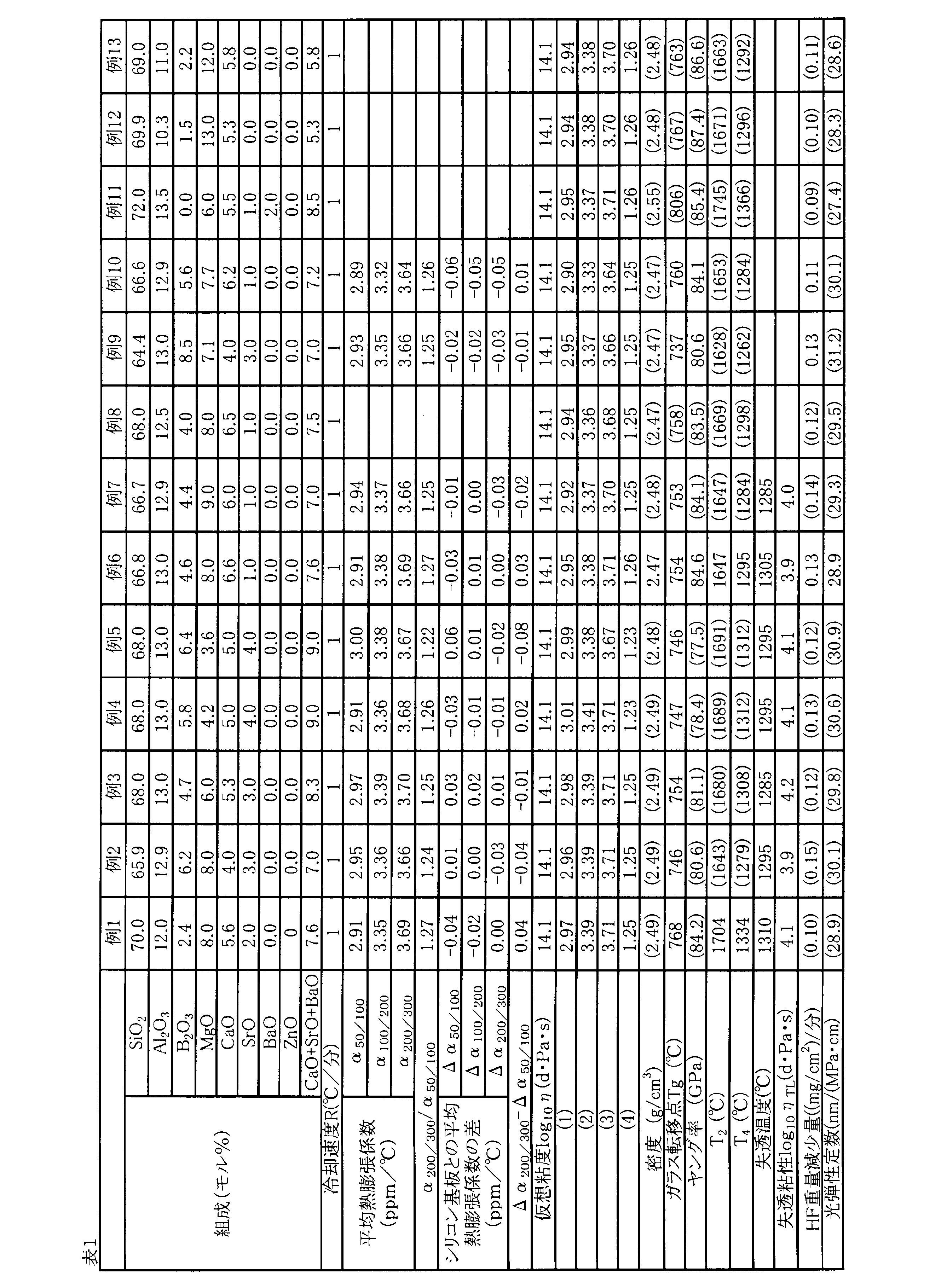
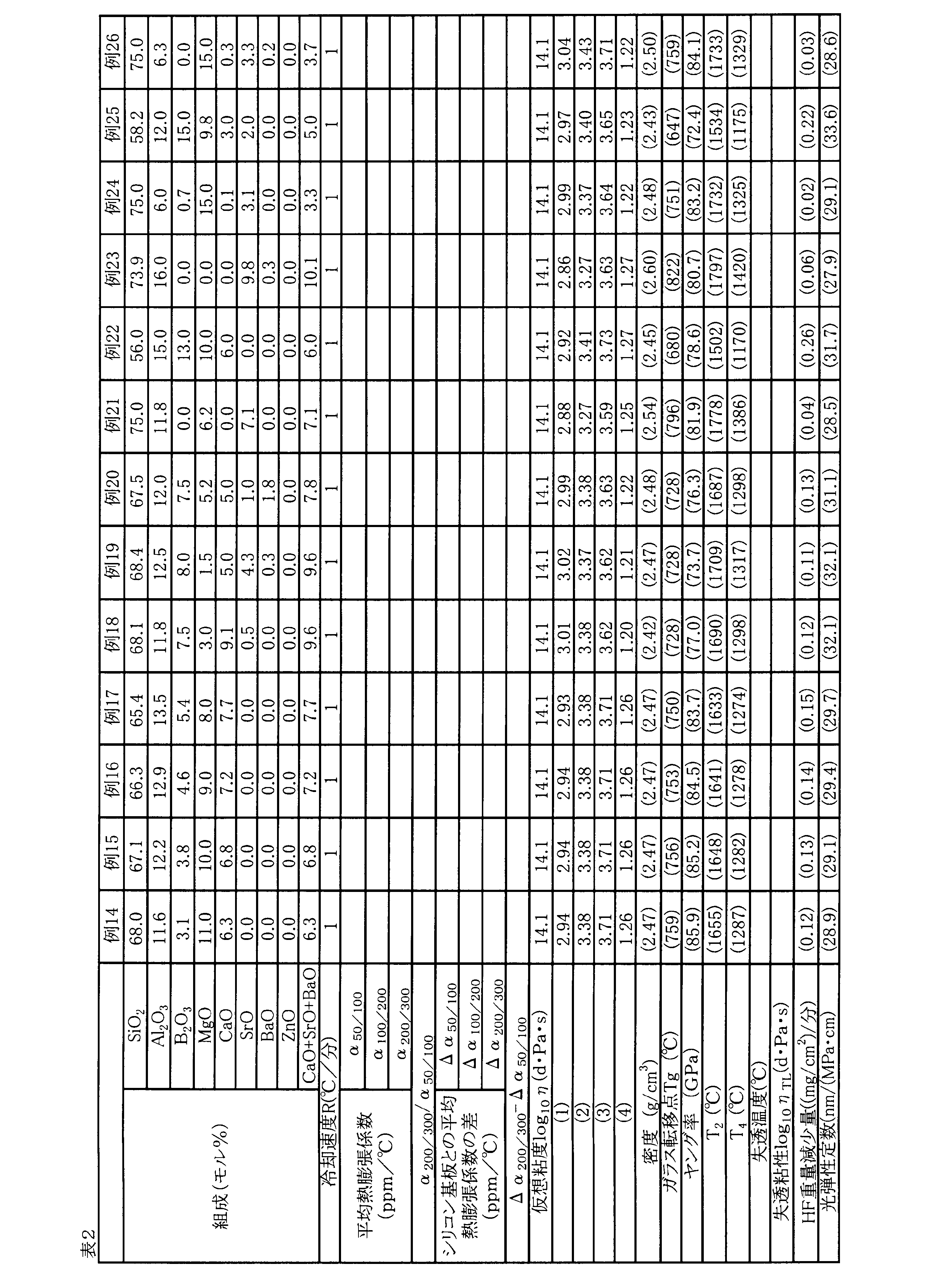
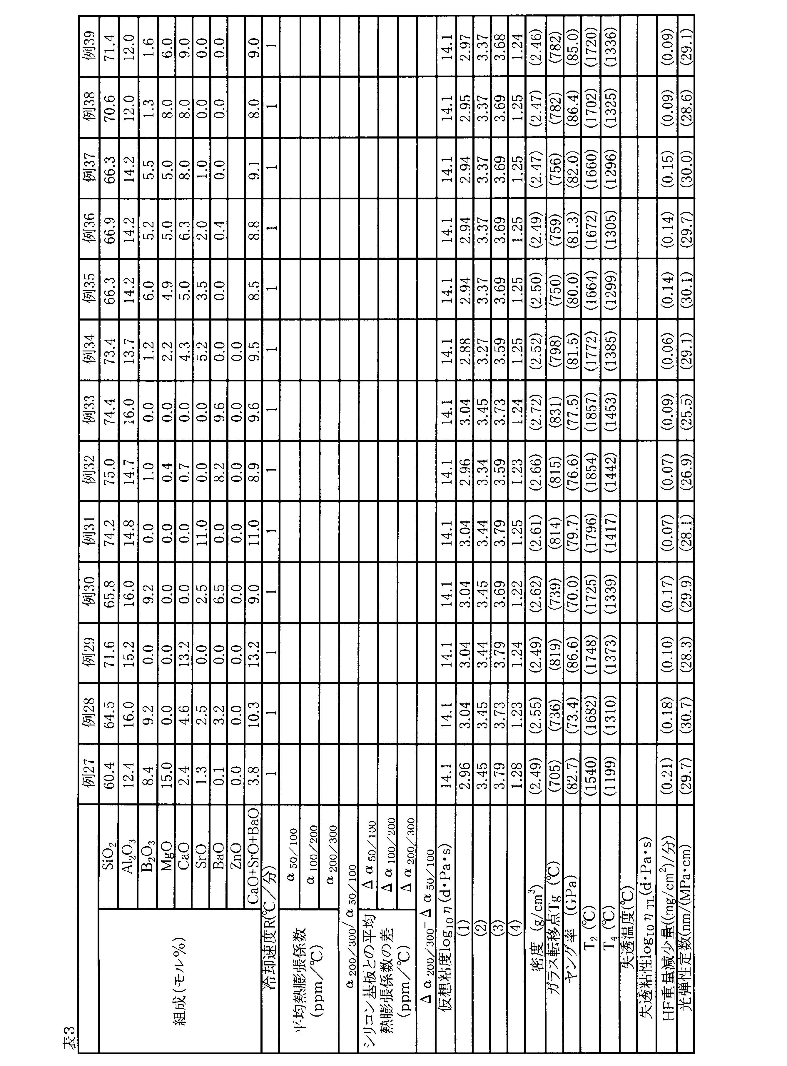

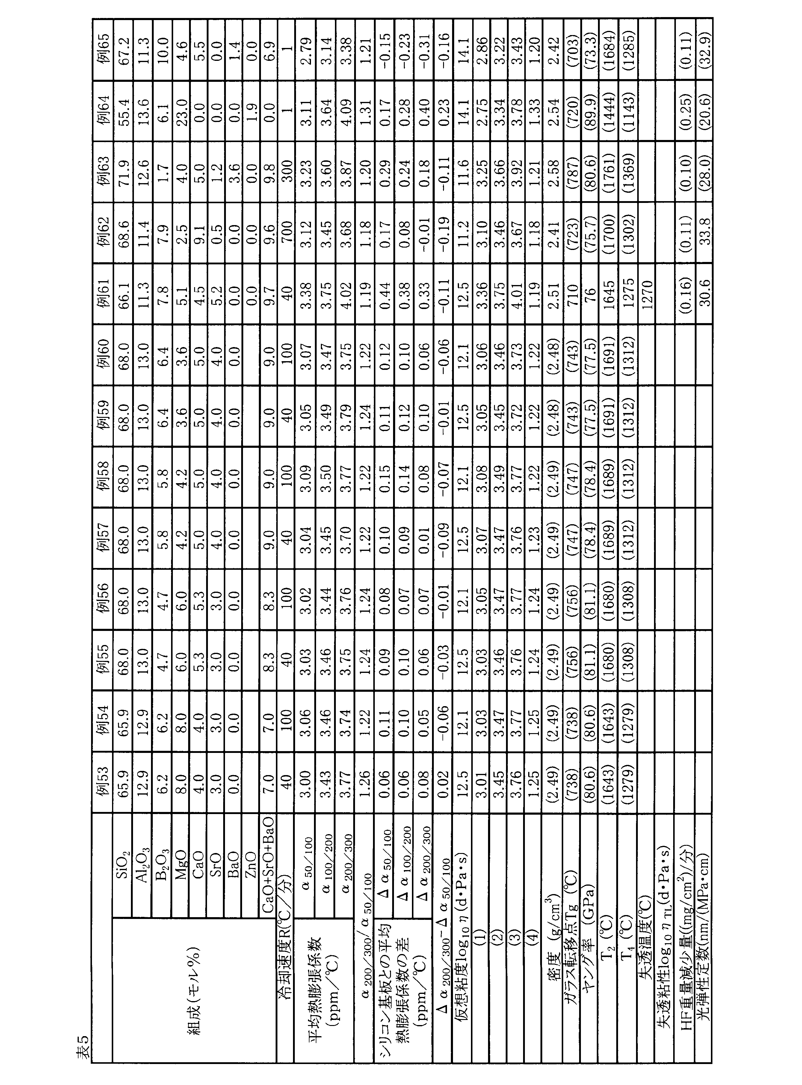
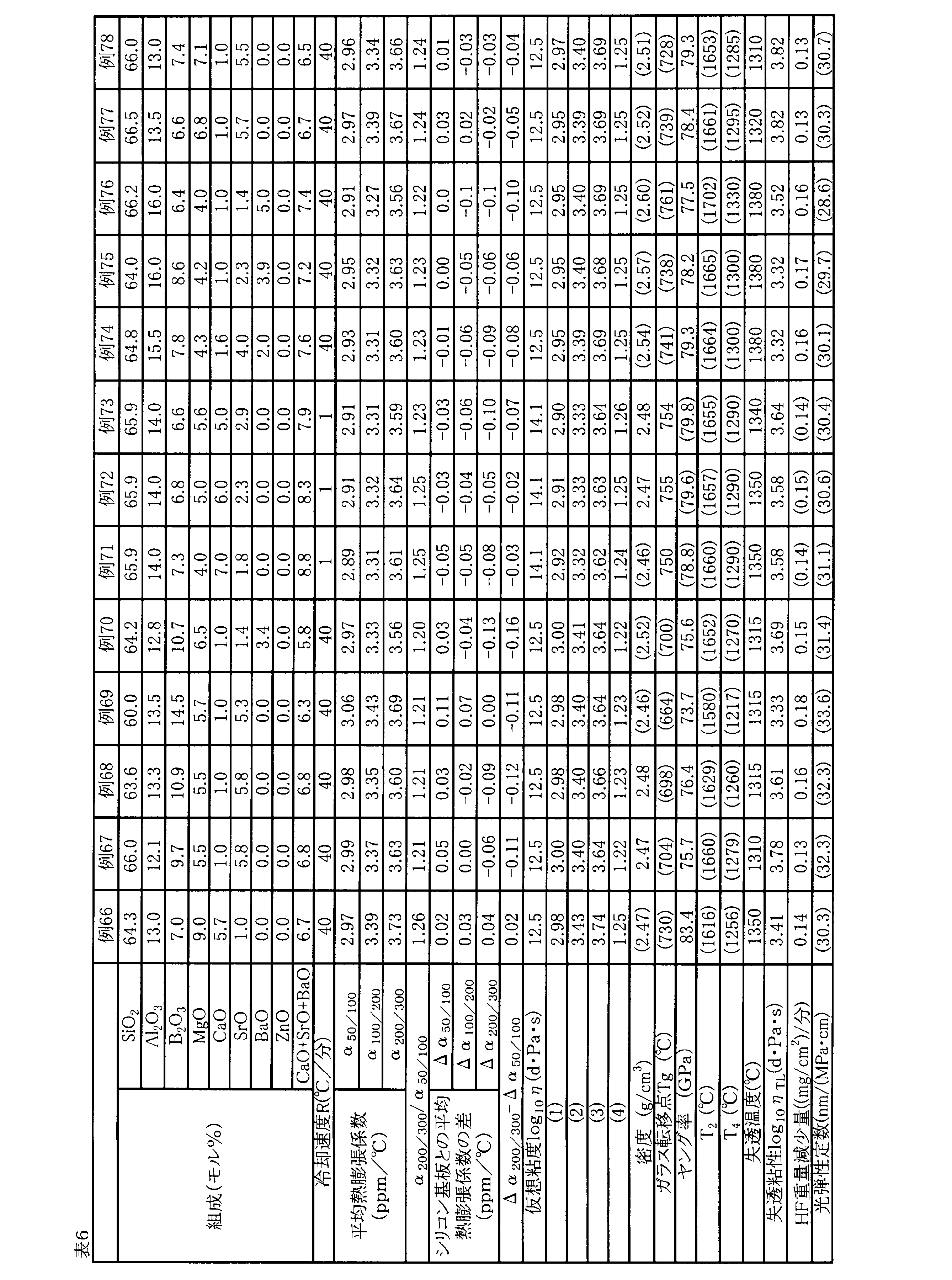

実施例である例1~60、66~87のガラス基板は、アルカリ金属酸化物の含有量が0.1%以下であるため、シリコン基板とガラス基板を貼り合わせる熱処理工程において、アルカリイオンがシリコン基板に拡散しない。また、50℃~100℃での平均熱膨張係数α50/100が2.70ppm/℃~3.20ppm/℃であり、200℃~300℃での平均熱膨張係数α200/300が3.45ppm/℃~3.95ppm/℃であり、α200/300をα50/100で除した値α200/300/α50/100が、1.20~1.30であるため、シリコン基板とガラス基板を貼り合わせる熱処理工程において、シリコン基板およびガラス基板に発生する残留歪が小さくなりやすい。
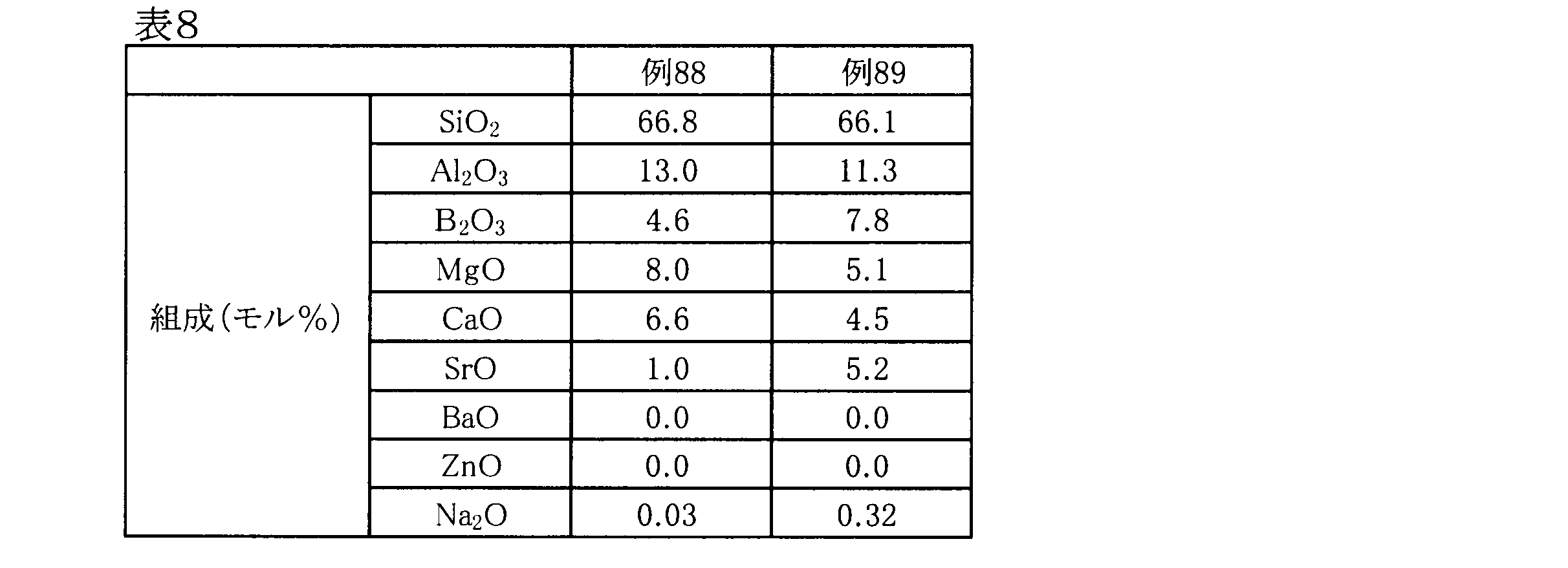
図1Aに示す、光選択透過型ガラス10の製造例を説明する。光選択透過型ガラス10は、直径15cmの円形で0.2mm厚のガラス基板12の片面に光選択透過層11を備える。
11,11a,11b 光選択透過層
111 吸収層
112,112a,112b,112c 反射層
12 ガラス基板
15 シリコン基板
16 光検出器アレイ
17 RGBモザイクカラーフィルタ
18 樹脂マイクロレンズ
19 固体撮像素子
21 接着剤
31 撮像レンズ
32 レンズユニット
33 筐体
40,50 積層基板
60 固体撮像装置(カメラモジュール)
Claims (21)
- ガラス基板と、
前記ガラス基板の少なくとも一方の主面に、近赤外線および可視光線のうち、近赤外線、可視光線、青の波長域の可視光線、赤の波長域の可視光線、および緑の波長域の可視光線の群から選ばれる少なくとも一を選択的に透過する光選択透過層を備え、
前記ガラス基板は、50℃~100℃での平均熱膨張係数α50/100が2.70ppm/℃~3.20ppm/℃であり、
200℃~300℃での平均熱膨張係数α200/300が3.45ppm/℃~3.95ppm/℃であり、
200℃~300℃の平均熱膨張係数α200/300を50℃~100℃の平均熱膨張係数α50/100で除した値α200/300/α50/100が、1.20~1.30であり、
アルカリ金属酸化物の含有量が酸化物基準のモル百分率表示で0%~0.1%である、光選択透過型ガラス。 - 前記ガラス基板の200℃~300℃での平均熱膨張係数α200/300が、3.55ppm/℃~3.85ppm/℃である、請求項1に記載の光選択透過型ガラス。
- 前記ガラス基板の組成が、酸化物基準のモル百分率表示で、下記である請求項1または2に記載の光選択透過型ガラス。
SiO2 :50%~75%、
Al2O3 :6%~16%、
B2O3 :0%~15%、
MgO :0%~15%、
CaO :0%~13%、
SrO :0%~11%、
BaO :0%~9.5% - 前記ガラス基板の組成が、酸化物基準のモル百分率表示で、CaO、SrO、およびBaOの合計含有量が7%以上、かつ(Al2O3の含有量)≧(MgOの含有量)であり、失透粘性が103.8d・Pa・s以上である、請求項1~3のいずれか一項に記載の光選択透過型ガラス。
- 前記ガラス基板の100℃~200℃での平均熱膨張係数α100/200が、3.13ppm/℃~3.63ppm/℃である、請求項1~4のいずれか一項に記載の光選択透過型ガラス。
- 前記ガラス基板中のFe2O3の含有量が、酸化物基準の質量百万分率表示で、200ppm以下である、請求項1~5のいずれか一項に記載の光選択透過型ガラス。
- 前記ガラス基板のヤング率が80GPa以上である、請求項1~6のいずれか一項に記載の光選択透過型ガラス。
- 前記ガラス基板の厚さが1.0mm以下である、請求項1~7のいずれか一項に記載の光選択透過型ガラス。
- 前記ガラス基板の面積が0.03m2以上である、請求項1~8のいずれか一項に記載の光選択透過型ガラス。
- 前記ガラス基板に含まれる0.5μm以上1mm以下の欠点の密度が1個/cm2以下である、請求項1~9のいずれか一項に記載の光選択透過型ガラス。
- 前記ガラス基板の仮想粘度が1011.0d・Pa・s~1014.1d・Pa・sである、請求項1~10のいずれか一項に記載の光選択透過型ガラス。
- 前記ガラス基板が、
0.0177×(SiO2の含有量)-0.0173×(Al2O3の含有量)+0.0377×(B2O3の含有量)+0.0771×(MgOの含有量)+0.1543×(CaOの含有量)+0.1808×(SrOの含有量)+0.2082×(BaOの含有量)+0.0344×(12.3+log1060-log10η)が2.70~3.20、
0.0181×(SiO2の含有量)+0.0004×(Al2O3の含有量)+0.0387×(B2O3の含有量)+0.0913×(MgOの含有量)+0.1621×(CaOの含有量)+0.1900×(SrOの含有量)+0.2180×(BaOの含有量)+0.0391×(12.3+log1060-log10η)が3.13~3.63、
0.0177×(SiO2の含有量)+0.0195×(Al2O3の含有量)+0.0323×(B2O3の含有量)+0.1015×(MgOの含有量)+0.1686×(CaOの含有量)+0.1990×(SrOの含有量)+0.2179×(BaOの含有量)+0.0312×(12.3+log1060-log10η)が3.45~3.95、および
0.0111×(SiO2の含有量)+0.0250×(Al2O3の含有量)+0.0078×(B2O3の含有量)+0.0144×(MgOの含有量)+0.0053×(CaOの含有量)+0.0052×(SrOの含有量)+0.0013×(BaOの含有量)-0.0041×(12.3+log1060-log10η)が1.20~1.30
を満たす、請求項1~11のいずれか一項に記載の光選択透過型ガラス。
(ここで、SiO2の含有量、Al2O3の含有量、B2O3の含有量、MgOの含有量、CaOの含有量、およびSrOの含有量は、得られたガラスに含有される酸化物基準のモル百分率表示で表した含有量、ηは仮想粘度(単位:d・Pa・s)である。) - 前記ガラス基板の25℃、5質量%のフッ酸水溶液に対する重量減少量が0.05(mg/cm2)/分以上、0.20(mg/cm2)/分以下である、請求項1~12のいずれか一項に記載の光選択透過型ガラス。
- 前記ガラス基板の光弾性定数が31nm/(MPa・cm)以下である、請求項1~13のいずれか一項に記載の光選択透過型ガラス。
- 前記光選択透過層として吸収層を備え、
前記吸収層は、透明樹脂と吸収色素を含有する、請求項1~14のいずれか1項に記載の光選択透過型ガラス。 - 前記吸収色素は、近赤外線吸収色素を含む、請求項15に記載の光選択透過型ガラス。
- 前記吸収色素は、近紫外線吸収色素を含む、請求項15または請求項16に記載の光選択透過型ガラス。
- 前記ガラス基板の少なくとも一方の主面に誘電体多層膜を有する反射層を備える、請求項1~17のいずれか1項に記載の光選択透過型ガラス。
- シリコン基板上に備えられた固体撮像素子と、請求項1~18いずれか1項に記載の光選択透過型ガラスと、を有する、積層基板。
- 光選択透過型ガラスとシリコン基板とが積層され、
前記光選択透過型ガラスは、ガラス基板と、前記ガラス基板の少なくとも一方の主面に、近赤外線および可視光線のうち、近赤外線、可視光線、青の波長域の可視光線、赤の波長域の可視光線、および緑の波長域の可視光線の群から選ばれる少なくとも一を選択的に透過する光選択透過層を備え、
前記ガラス基板の50℃~100℃の平均熱膨張係数α50/100と、前記シリコン基板の50℃~100℃の平均熱膨張係数αSi50/100との差Δα50/100(=α50/100-αSi50/100)が、-0.25ppm/℃~0.25ppm/℃であり、
前記ガラス基板の200℃~300℃の平均熱膨張係数α200/300と、前記シリコン基板の200℃~300℃の平均熱膨張係数αSi200/300との差Δα200/300(=α200/300-αSi200/300)が、-0.25ppm/℃~0.25ppm/℃であり、
Δα200/300-Δα50/100が-0.16ppm/℃~0.16ppm/℃であり、
前記ガラス基板のアルカリ金属酸化物の含有量が酸化物基準のモル百分率表示で0%~0.1%である積層基板。 - 前記ガラス基板の100℃~200℃の平均熱膨張係数α100/200と、前記シリコン基板の100℃~200℃の平均熱膨張係数αSi100/200との差Δα100/200(=α100/200-αSi100/200)が、-0.25ppm/℃~0.25ppm/℃である請求項20に記載の積層基板。
Priority Applications (4)
| Application Number | Priority Date | Filing Date | Title |
|---|---|---|---|
| KR1020177021666A KR20170110619A (ko) | 2015-02-06 | 2016-02-02 | 광 선택 투과형 유리 및 적층 기판 |
| JP2016573378A JPWO2016125792A1 (ja) | 2015-02-06 | 2016-02-02 | 光選択透過型ガラスおよび積層基板 |
| CN201680008864.5A CN107207324A (zh) | 2015-02-06 | 2016-02-02 | 光选择透射型玻璃和层叠基板 |
| US15/667,191 US10683233B2 (en) | 2015-02-06 | 2017-08-02 | Light selective transmission type glass and laminated substrate |
Applications Claiming Priority (4)
| Application Number | Priority Date | Filing Date | Title |
|---|---|---|---|
| JP2015022719 | 2015-02-06 | ||
| JP2015-022719 | 2015-02-06 | ||
| JP2015241303 | 2015-12-10 | ||
| JP2015-241303 | 2015-12-10 |
Related Child Applications (1)
| Application Number | Title | Priority Date | Filing Date |
|---|---|---|---|
| US15/667,191 Continuation US10683233B2 (en) | 2015-02-06 | 2017-08-02 | Light selective transmission type glass and laminated substrate |
Publications (1)
| Publication Number | Publication Date |
|---|---|
| WO2016125792A1 true WO2016125792A1 (ja) | 2016-08-11 |
Family
ID=56564128
Family Applications (2)
| Application Number | Title | Priority Date | Filing Date |
|---|---|---|---|
| PCT/JP2016/053055 Ceased WO2016125792A1 (ja) | 2015-02-06 | 2016-02-02 | 光選択透過型ガラスおよび積層基板 |
| PCT/JP2016/053047 Ceased WO2016125787A1 (ja) | 2015-02-06 | 2016-02-02 | ガラス基板、積層基板、およびガラス基板の製造方法 |
Family Applications After (1)
| Application Number | Title | Priority Date | Filing Date |
|---|---|---|---|
| PCT/JP2016/053047 Ceased WO2016125787A1 (ja) | 2015-02-06 | 2016-02-02 | ガラス基板、積層基板、およびガラス基板の製造方法 |
Country Status (6)
| Country | Link |
|---|---|
| US (2) | US10759691B2 (ja) |
| JP (2) | JPWO2016125792A1 (ja) |
| KR (2) | KR20170110619A (ja) |
| CN (2) | CN107207324A (ja) |
| TW (2) | TWI675018B (ja) |
| WO (2) | WO2016125792A1 (ja) |
Cited By (8)
| Publication number | Priority date | Publication date | Assignee | Title |
|---|---|---|---|---|
| CN107721156A (zh) * | 2017-03-31 | 2018-02-23 | 旭硝子株式会社 | 无碱玻璃基板 |
| WO2018135189A1 (ja) * | 2017-01-20 | 2018-07-26 | ソニーセミコンダクタソリューションズ株式会社 | 表示装置、電子機器、及び表示装置の製造方法 |
| JP2018163327A (ja) * | 2017-03-27 | 2018-10-18 | プラチナム オプティクス テクノロジー (スーチョウ) インコーポレイテッドPlatinum Optics Technology (Suzhou) Inc. | フィルタ |
| JP2018188336A (ja) * | 2017-05-08 | 2018-11-29 | Agc株式会社 | 積層ガラス、積層基板および積層基板の製造方法 |
| JP2019056823A (ja) * | 2017-09-21 | 2019-04-11 | 日本電気硝子株式会社 | ホルダ付き赤外線吸収ガラス |
| KR20190059240A (ko) * | 2017-11-22 | 2019-05-30 | 쇼오트 아게 | 광학 필터용 기판 및 광학 필터 |
| WO2021009587A1 (ja) * | 2019-07-12 | 2021-01-21 | 株式会社半導体エネルギー研究所 | 機能パネル、表示装置、入出力装置、情報処理装置 |
| JP2022070521A (ja) * | 2020-10-27 | 2022-05-13 | 株式会社Nsc | 機能膜付き基板の製造方法 |
Families Citing this family (31)
| Publication number | Priority date | Publication date | Assignee | Title |
|---|---|---|---|---|
| US20180141857A1 (en) * | 2015-05-15 | 2018-05-24 | Nippon Electric Glass Co., Ltd. | Strengthened glass plate producing method, glass plate for strengthening, and strengthened glass plate |
| CN109716176B (zh) * | 2016-06-07 | 2021-09-17 | 艾瑞3D 有限公司 | 用于深度采集和三维成像的光场成像装置和方法 |
| WO2018025727A1 (ja) * | 2016-08-05 | 2018-02-08 | 旭硝子株式会社 | 無アルカリガラス基板、積層基板、およびガラス基板の製造方法 |
| KR20190054068A (ko) * | 2016-09-16 | 2019-05-21 | 에이지씨 가부시키가이샤 | 유리 기판 및 적층 기판 |
| JP6770915B2 (ja) * | 2017-03-08 | 2020-10-21 | 株式会社Screenホールディングス | 熱処理装置 |
| US11401199B2 (en) * | 2017-04-17 | 2022-08-02 | Nippon Electric Glass Co., Ltd. | Glass plate |
| CN111225883A (zh) * | 2017-10-25 | 2020-06-02 | 日本板硝子株式会社 | 玻璃组合物 |
| CN111344311B (zh) * | 2017-11-24 | 2023-01-31 | 迪睿合株式会社 | 光固化性树脂组合物及图像显示装置的制造方法 |
| US11554984B2 (en) * | 2018-02-22 | 2023-01-17 | Corning Incorporated | Alkali-free borosilicate glasses with low post-HF etch roughness |
| KR101924174B1 (ko) * | 2018-04-04 | 2019-02-22 | (주)유티아이 | 근적외선 필터 및 그 필터의 제조방법 |
| CN108614318B (zh) * | 2018-04-23 | 2019-12-24 | 安徽帝显电子有限公司 | 一种车载用导光膜及其制备方法 |
| WO2019205938A1 (zh) * | 2018-04-25 | 2019-10-31 | 成都光明光电股份有限公司 | 玻璃组合物 |
| TWI676853B (zh) * | 2018-07-25 | 2019-11-11 | 白金科技股份有限公司 | 濾光片 |
| KR102205956B1 (ko) * | 2018-08-01 | 2021-01-21 | 인하공업전문대학산학협력단 | 유연성 소자 제조용 유리기판-금속기판 접합체의 제조방법 |
| US11114483B2 (en) * | 2018-08-10 | 2021-09-07 | Omnivision Technologies, Inc. | Cavityless chip-scale image-sensor package |
| SG11202102686WA (en) * | 2018-09-21 | 2021-04-29 | Schott Glass Technologies Suzhou Co Ltd | Collimating system for providing highly efficient parallel light |
| CN111338171A (zh) * | 2018-12-19 | 2020-06-26 | 青岛海信激光显示股份有限公司 | 一种投影屏幕及激光投影装置 |
| WO2020125317A1 (zh) * | 2018-12-19 | 2020-06-25 | 青岛海信激光显示股份有限公司 | 一种投影屏幕及激光投影装置 |
| CN117209137A (zh) * | 2019-04-12 | 2023-12-12 | Agc株式会社 | 无碱玻璃和玻璃板 |
| US11070786B2 (en) * | 2019-05-02 | 2021-07-20 | Disney Enterprises, Inc. | Illumination-based system for distributing immersive experience content in a multi-user environment |
| KR20220025018A (ko) * | 2019-06-26 | 2022-03-03 | 코닝 인코포레이티드 | 열 이력에 둔감한 무알칼리 유리들 |
| WO2021019654A1 (ja) * | 2019-07-29 | 2021-02-04 | Agc株式会社 | 支持ガラス基板 |
| US11327084B2 (en) * | 2019-09-19 | 2022-05-10 | Invidx Corp. | Joint hematology and biochemistry point-of-care testing system |
| US11161109B2 (en) | 2019-09-19 | 2021-11-02 | Invidx Corp. | Point-of-care testing cartridge with sliding cap |
| US11997766B2 (en) | 2019-10-11 | 2024-05-28 | Semiconductor Energy Laboratory Co., Ltd. | Functional panel, display device, input/output device, and data processing device |
| WO2021192700A1 (ja) * | 2020-03-23 | 2021-09-30 | Agc株式会社 | 接合体 |
| JP7782443B2 (ja) * | 2020-06-10 | 2025-12-09 | Agc株式会社 | 積層部材 |
| US12560749B2 (en) * | 2020-10-06 | 2026-02-24 | Viavi Solutions Inc. | Communal optical filter and other optical filters on substrate |
| CN115872617A (zh) * | 2021-09-29 | 2023-03-31 | 成都光明光电股份有限公司 | 玻璃组合物 |
| CN114551365B (zh) * | 2022-02-17 | 2026-01-13 | 常州银河世纪微电子股份有限公司 | 抗红外的可见光传感器封装材料及抗红外的可见光传感器 |
| CN115857257A (zh) * | 2022-11-16 | 2023-03-28 | 北京空间机电研究所 | 一种提高空间低温光学系统温度稳定性的冷窗组件 |
Citations (7)
| Publication number | Priority date | Publication date | Assignee | Title |
|---|---|---|---|---|
| JP2004315354A (ja) * | 2003-03-31 | 2004-11-11 | Asahi Glass Co Ltd | 無アルカリガラス |
| JP2009286689A (ja) * | 2008-05-30 | 2009-12-10 | Corning Inc | ボロアルミノシリケートガラス |
| WO2010107111A1 (ja) * | 2009-03-19 | 2010-09-23 | 日本電気硝子株式会社 | 無アルカリガラス |
| JP2011020864A (ja) * | 2009-07-13 | 2011-02-03 | Nippon Electric Glass Co Ltd | ガラス基板の製造方法 |
| WO2013099970A1 (ja) * | 2011-12-28 | 2013-07-04 | AvanStrate株式会社 | フラットパネルディスプレイ用ガラス基板およびその製造方法 |
| WO2013183681A1 (ja) * | 2012-06-07 | 2013-12-12 | 旭硝子株式会社 | 無アルカリガラスおよびこれを用いた無アルカリガラス板 |
| JP2013257532A (ja) * | 2012-03-22 | 2013-12-26 | Nippon Shokubai Co Ltd | 光選択透過フィルター、樹脂シート及び固体撮像素子 |
Family Cites Families (9)
| Publication number | Priority date | Publication date | Assignee | Title |
|---|---|---|---|---|
| JP3153710B2 (ja) | 1994-01-21 | 2001-04-09 | ホーヤ株式会社 | シリコン台座用ガラス及びシリコン基材型センサー |
| KR20050109929A (ko) * | 2003-03-31 | 2005-11-22 | 아사히 가라스 가부시키가이샤 | 무알칼리 유리 |
| JP5435394B2 (ja) | 2007-06-08 | 2014-03-05 | 日本電気硝子株式会社 | 強化ガラス基板及びその製造方法 |
| JP3153710U (ja) | 2009-07-03 | 2009-09-17 | モリト株式会社 | 折畳み式包装箱 |
| KR20130098877A (ko) | 2010-06-03 | 2013-09-05 | 아사히 가라스 가부시키가이샤 | 유리 기판 및 그의 제조 방법 |
| US9227295B2 (en) * | 2011-05-27 | 2016-01-05 | Corning Incorporated | Non-polished glass wafer, thinning system and method for using the non-polished glass wafer to thin a semiconductor wafer |
| CA2838581A1 (en) | 2011-06-06 | 2012-12-13 | Asahi Glass Company, Limited | Optical filter, solid-state imaging element, imaging device lens and imaging device |
| KR102059198B1 (ko) * | 2012-03-22 | 2019-12-24 | 가부시키가이샤 닛폰 쇼쿠바이 | 광 선택 투과 필터, 수지 시트 및 고체 촬상 소자 |
| WO2014034386A1 (ja) | 2012-08-29 | 2014-03-06 | 旭硝子株式会社 | 近赤外線カットフィルタ |
-
2016
- 2016-02-02 KR KR1020177021666A patent/KR20170110619A/ko not_active Withdrawn
- 2016-02-02 JP JP2016573378A patent/JPWO2016125792A1/ja active Pending
- 2016-02-02 CN CN201680008864.5A patent/CN107207324A/zh active Pending
- 2016-02-02 KR KR1020177021773A patent/KR102538464B1/ko active Active
- 2016-02-02 WO PCT/JP2016/053055 patent/WO2016125792A1/ja not_active Ceased
- 2016-02-02 JP JP2016573375A patent/JP6604337B2/ja active Active
- 2016-02-02 WO PCT/JP2016/053047 patent/WO2016125787A1/ja not_active Ceased
- 2016-02-02 CN CN201680008835.9A patent/CN107207323B/zh active Active
- 2016-02-05 TW TW105104200A patent/TWI675018B/zh active
- 2016-02-05 TW TW105104171A patent/TW201639800A/zh unknown
-
2017
- 2017-08-02 US US15/666,862 patent/US10759691B2/en active Active
- 2017-08-02 US US15/667,191 patent/US10683233B2/en active Active
Patent Citations (7)
| Publication number | Priority date | Publication date | Assignee | Title |
|---|---|---|---|---|
| JP2004315354A (ja) * | 2003-03-31 | 2004-11-11 | Asahi Glass Co Ltd | 無アルカリガラス |
| JP2009286689A (ja) * | 2008-05-30 | 2009-12-10 | Corning Inc | ボロアルミノシリケートガラス |
| WO2010107111A1 (ja) * | 2009-03-19 | 2010-09-23 | 日本電気硝子株式会社 | 無アルカリガラス |
| JP2011020864A (ja) * | 2009-07-13 | 2011-02-03 | Nippon Electric Glass Co Ltd | ガラス基板の製造方法 |
| WO2013099970A1 (ja) * | 2011-12-28 | 2013-07-04 | AvanStrate株式会社 | フラットパネルディスプレイ用ガラス基板およびその製造方法 |
| JP2013257532A (ja) * | 2012-03-22 | 2013-12-26 | Nippon Shokubai Co Ltd | 光選択透過フィルター、樹脂シート及び固体撮像素子 |
| WO2013183681A1 (ja) * | 2012-06-07 | 2013-12-12 | 旭硝子株式会社 | 無アルカリガラスおよびこれを用いた無アルカリガラス板 |
Cited By (28)
| Publication number | Priority date | Publication date | Assignee | Title |
|---|---|---|---|---|
| CN110199572A (zh) * | 2017-01-20 | 2019-09-03 | 索尼半导体解决方案公司 | 显示装置、电子设备及制造显示装置的方法 |
| WO2018135189A1 (ja) * | 2017-01-20 | 2018-07-26 | ソニーセミコンダクタソリューションズ株式会社 | 表示装置、電子機器、及び表示装置の製造方法 |
| JP7186620B2 (ja) | 2017-01-20 | 2022-12-09 | ソニーセミコンダクタソリューションズ株式会社 | 表示装置、電子機器、及び表示装置の製造方法 |
| US11769773B2 (en) | 2017-01-20 | 2023-09-26 | Sony Semiconductor Solutions Corporation | Display device, electronic device, and method of manufacturing display device with substrate including light emitting elements adhered to substrate including microlens array |
| US11024651B2 (en) | 2017-01-20 | 2021-06-01 | Sony Semiconductor Solutions Corporation | Display device and electronic device with microlens array and light emitting element substrates bonded by adhesive layer |
| CN110199572B (zh) * | 2017-01-20 | 2024-01-26 | 索尼半导体解决方案公司 | 显示装置、电子设备及制造显示装置的方法 |
| US20190363107A1 (en) * | 2017-01-20 | 2019-11-28 | Sony Semiconductor Solutions Corporation | Display device, electronic device, and method of manufacturing display device |
| JPWO2018135189A1 (ja) * | 2017-01-20 | 2019-11-07 | ソニーセミコンダクタソリューションズ株式会社 | 表示装置、電子機器、及び表示装置の製造方法 |
| JP2018163327A (ja) * | 2017-03-27 | 2018-10-18 | プラチナム オプティクス テクノロジー (スーチョウ) インコーポレイテッドPlatinum Optics Technology (Suzhou) Inc. | フィルタ |
| US10640416B2 (en) | 2017-03-31 | 2020-05-05 | AGC Inc. | Alkali-free glass substrate |
| KR102535060B1 (ko) * | 2017-03-31 | 2023-05-23 | 에이지씨 가부시키가이샤 | 무알칼리 유리 기판 |
| CN107721156A (zh) * | 2017-03-31 | 2018-02-23 | 旭硝子株式会社 | 无碱玻璃基板 |
| JP2018172226A (ja) * | 2017-03-31 | 2018-11-08 | Agc株式会社 | 無アルカリガラス基板 |
| KR20180111597A (ko) * | 2017-03-31 | 2018-10-11 | 에이지씨 가부시키가이샤 | 무알칼리 유리 기판 |
| JP2018188336A (ja) * | 2017-05-08 | 2018-11-29 | Agc株式会社 | 積層ガラス、積層基板および積層基板の製造方法 |
| JP2019056823A (ja) * | 2017-09-21 | 2019-04-11 | 日本電気硝子株式会社 | ホルダ付き赤外線吸収ガラス |
| JP7077554B2 (ja) | 2017-09-21 | 2022-05-31 | 日本電気硝子株式会社 | ホルダ付き赤外線吸収ガラス |
| KR102001788B1 (ko) | 2017-11-22 | 2019-07-18 | 쇼오트 아게 | 광학 필터용 기판 및 광학 필터 |
| KR20190059240A (ko) * | 2017-11-22 | 2019-05-30 | 쇼오트 아게 | 광학 필터용 기판 및 광학 필터 |
| JPWO2021009587A1 (ja) * | 2019-07-12 | 2021-01-21 | ||
| US11844236B2 (en) | 2019-07-12 | 2023-12-12 | Semiconductor Energy Laboratory Co., Ltd. | Functional panel, display device, input/output device, and data processing device |
| WO2021009587A1 (ja) * | 2019-07-12 | 2021-01-21 | 株式会社半導体エネルギー研究所 | 機能パネル、表示装置、入出力装置、情報処理装置 |
| JP7530897B2 (ja) | 2019-07-12 | 2024-08-08 | 株式会社半導体エネルギー研究所 | 機能パネル、表示装置、入出力装置、情報処理装置 |
| JP2024149544A (ja) * | 2019-07-12 | 2024-10-18 | 株式会社半導体エネルギー研究所 | 機能パネル |
| US12256597B2 (en) | 2019-07-12 | 2025-03-18 | Semiconductor Energy Laboratory Co., Ltd. | Functional panel, display device, input/output device, and data processing device |
| JP7773594B2 (ja) | 2019-07-12 | 2025-11-19 | 株式会社半導体エネルギー研究所 | 機能パネル |
| JP2022070521A (ja) * | 2020-10-27 | 2022-05-13 | 株式会社Nsc | 機能膜付き基板の製造方法 |
| JP7569070B2 (ja) | 2020-10-27 | 2024-10-17 | 株式会社Nsc | 機能膜付き基板の製造方法 |
Also Published As
| Publication number | Publication date |
|---|---|
| CN107207323B (zh) | 2020-12-11 |
| JPWO2016125787A1 (ja) | 2017-12-14 |
| TW201639800A (zh) | 2016-11-16 |
| US20170327408A1 (en) | 2017-11-16 |
| US20170355637A1 (en) | 2017-12-14 |
| TWI675018B (zh) | 2019-10-21 |
| KR20170110619A (ko) | 2017-10-11 |
| TW201708142A (zh) | 2017-03-01 |
| CN107207324A (zh) | 2017-09-26 |
| JPWO2016125792A1 (ja) | 2017-12-14 |
| CN107207323A (zh) | 2017-09-26 |
| US10759691B2 (en) | 2020-09-01 |
| JP6604337B2 (ja) | 2019-11-13 |
| KR20170115537A (ko) | 2017-10-17 |
| KR102538464B1 (ko) | 2023-06-01 |
| US10683233B2 (en) | 2020-06-16 |
| WO2016125787A1 (ja) | 2016-08-11 |
Similar Documents
| Publication | Publication Date | Title |
|---|---|---|
| US10683233B2 (en) | Light selective transmission type glass and laminated substrate | |
| US9470820B2 (en) | Microlens array, image pickup element package, and method for manufacturing microlens array | |
| JP6772450B2 (ja) | 近赤外線吸収型ガラスウェハおよび半導体ウェハ積層体 | |
| JP5849719B2 (ja) | 光吸収体及びこれを用いた撮像装置 | |
| JP7251423B2 (ja) | 光学部材及びカメラモジュール | |
| CN110873914B (zh) | 光学滤波器及其制造方法、固体摄像装置及相机模块 | |
| CN112585508B (zh) | 光学滤波器、固体摄像装置及照相机模块 | |
| WO2016114363A1 (ja) | 近赤外線カットフィルタおよび撮像装置 | |
| JP2020109496A (ja) | 光学フィルタおよび近赤外線カットフィルタ | |
| CN110018538B (zh) | 光学滤光器单元阵列结构体及其制造方法 | |
| WO2011055726A1 (ja) | 近赤外線カットフィルタ | |
| JP2017072748A (ja) | 光学フィルターおよび光学フィルターを用いた撮像素子 | |
| CN110073247A (zh) | 光学元件、成像元件封装、成像装置和电子设备 | |
| CN108693584B (zh) | 光学滤光片及使用光学滤光片的固体摄像装置 | |
| JP2017167557A (ja) | 光吸収体及びこれを用いた撮像装置 | |
| JP2005353718A (ja) | 半導体パッケージの窓用ガラス、半導体パッケージ用ガラス窓および半導体パッケージ | |
| US12449580B2 (en) | Near-infrared cut filter and imaging apparatus | |
| JP4433391B2 (ja) | 半導体パッケージの窓用ガラス、半導体パッケージ用ガラス窓および半導体パッケージ | |
| JP2024041789A (ja) | 光学フィルタ、近赤外線カットフィルタ、および撮像装置 | |
| JP2011049275A (ja) | 固体撮像素子パッケージ用窓材並びに撮像装置 | |
| KR102303249B1 (ko) | 강화 유리기재를 포함하는 근적외선 흡수원판 및 이를 포함하는 광학필터 | |
| US20230367050A1 (en) | Near-infrared cut filter and imaging device having same | |
| US20250362567A1 (en) | Optical substrate and solid state imaging device package | |
| JPH09283731A (ja) | 固体撮像素子用カバーガラス | |
| US20250189706A1 (en) | Optical filter |
Legal Events
| Date | Code | Title | Description |
|---|---|---|---|
| 121 | Ep: the epo has been informed by wipo that ep was designated in this application |
Ref document number: 16746623 Country of ref document: EP Kind code of ref document: A1 |
|
| ENP | Entry into the national phase |
Ref document number: 2016573378 Country of ref document: JP Kind code of ref document: A Ref document number: 20177021666 Country of ref document: KR Kind code of ref document: A |
|
| NENP | Non-entry into the national phase |
Ref country code: DE |
|
| 122 | Ep: pct application non-entry in european phase |
Ref document number: 16746623 Country of ref document: EP Kind code of ref document: A1 |