WO2016079995A1 - 半導体装置及びパワーモジュール - Google Patents
半導体装置及びパワーモジュール Download PDFInfo
- Publication number
- WO2016079995A1 WO2016079995A1 PCT/JP2015/005799 JP2015005799W WO2016079995A1 WO 2016079995 A1 WO2016079995 A1 WO 2016079995A1 JP 2015005799 W JP2015005799 W JP 2015005799W WO 2016079995 A1 WO2016079995 A1 WO 2016079995A1
- Authority
- WO
- WIPO (PCT)
- Prior art keywords
- heat sink
- semiconductor device
- bus bar
- electrical connection
- heat
- Prior art date
- Legal status (The legal status is an assumption and is not a legal conclusion. Google has not performed a legal analysis and makes no representation as to the accuracy of the status listed.)
- Ceased
Links
Images






Classifications
-
- H—ELECTRICITY
- H10—SEMICONDUCTOR DEVICES; ELECTRIC SOLID-STATE DEVICES NOT OTHERWISE PROVIDED FOR
- H10W—GENERIC PACKAGES, INTERCONNECTIONS, CONNECTORS OR OTHER CONSTRUCTIONAL DETAILS OF DEVICES COVERED BY CLASS H10
- H10W40/00—Arrangements for thermal protection or thermal control
- H10W40/20—Arrangements for cooling
- H10W40/22—Arrangements for cooling characterised by their shape, e.g. having conical or cylindrical projections
-
- H—ELECTRICITY
- H02—GENERATION; CONVERSION OR DISTRIBUTION OF ELECTRIC POWER
- H02P—CONTROL OR REGULATION OF ELECTRIC MOTORS, ELECTRIC GENERATORS OR DYNAMO-ELECTRIC CONVERTERS; CONTROLLING TRANSFORMERS, REACTORS OR CHOKE COILS
- H02P27/00—Arrangements or methods for the control of AC motors characterised by the kind of supply voltage
- H02P27/04—Arrangements or methods for the control of AC motors characterised by the kind of supply voltage using variable-frequency supply voltage, e.g. inverter or converter supply voltage
- H02P27/06—Arrangements or methods for the control of AC motors characterised by the kind of supply voltage using variable-frequency supply voltage, e.g. inverter or converter supply voltage using DC to AC converters or inverters
-
- H—ELECTRICITY
- H10—SEMICONDUCTOR DEVICES; ELECTRIC SOLID-STATE DEVICES NOT OTHERWISE PROVIDED FOR
- H10W—GENERIC PACKAGES, INTERCONNECTIONS, CONNECTORS OR OTHER CONSTRUCTIONAL DETAILS OF DEVICES COVERED BY CLASS H10
- H10W70/00—Package substrates; Interposers; Redistribution layers [RDL]
- H10W70/40—Leadframes
- H10W70/461—Leadframes specially adapted for cooling
-
- H—ELECTRICITY
- H10—SEMICONDUCTOR DEVICES; ELECTRIC SOLID-STATE DEVICES NOT OTHERWISE PROVIDED FOR
- H10W—GENERIC PACKAGES, INTERCONNECTIONS, CONNECTORS OR OTHER CONSTRUCTIONAL DETAILS OF DEVICES COVERED BY CLASS H10
- H10W70/00—Package substrates; Interposers; Redistribution layers [RDL]
- H10W70/40—Leadframes
- H10W70/464—Additional interconnections in combination with leadframes
- H10W70/466—Tape carriers or flat leads
-
- H—ELECTRICITY
- H10—SEMICONDUCTOR DEVICES; ELECTRIC SOLID-STATE DEVICES NOT OTHERWISE PROVIDED FOR
- H10W—GENERIC PACKAGES, INTERCONNECTIONS, CONNECTORS OR OTHER CONSTRUCTIONAL DETAILS OF DEVICES COVERED BY CLASS H10
- H10W72/00—Interconnections or connectors in packages
-
- H—ELECTRICITY
- H10—SEMICONDUCTOR DEVICES; ELECTRIC SOLID-STATE DEVICES NOT OTHERWISE PROVIDED FOR
- H10W—GENERIC PACKAGES, INTERCONNECTIONS, CONNECTORS OR OTHER CONSTRUCTIONAL DETAILS OF DEVICES COVERED BY CLASS H10
- H10W74/00—Encapsulations, e.g. protective coatings
- H10W74/10—Encapsulations, e.g. protective coatings characterised by their shape or disposition
- H10W74/111—Encapsulations, e.g. protective coatings characterised by their shape or disposition the semiconductor body being completely enclosed
- H10W74/129—Encapsulations, e.g. protective coatings characterised by their shape or disposition the semiconductor body being completely enclosed forming a chip-scale package [CSP]
-
- H—ELECTRICITY
- H10—SEMICONDUCTOR DEVICES; ELECTRIC SOLID-STATE DEVICES NOT OTHERWISE PROVIDED FOR
- H10W—GENERIC PACKAGES, INTERCONNECTIONS, CONNECTORS OR OTHER CONSTRUCTIONAL DETAILS OF DEVICES COVERED BY CLASS H10
- H10W76/00—Containers; Fillings or auxiliary members therefor; Seals
- H10W76/10—Containers or parts thereof
- H10W76/12—Containers or parts thereof characterised by their shape
- H10W76/13—Containers comprising a conductive base serving as an interconnection
- H10W76/138—Containers comprising a conductive base serving as an interconnection having another interconnection being formed by a cover plate parallel to the conductive base, e.g. sandwich type
-
- H—ELECTRICITY
- H10—SEMICONDUCTOR DEVICES; ELECTRIC SOLID-STATE DEVICES NOT OTHERWISE PROVIDED FOR
- H10W—GENERIC PACKAGES, INTERCONNECTIONS, CONNECTORS OR OTHER CONSTRUCTIONAL DETAILS OF DEVICES COVERED BY CLASS H10
- H10W90/00—Package configurations
-
- H—ELECTRICITY
- H10—SEMICONDUCTOR DEVICES; ELECTRIC SOLID-STATE DEVICES NOT OTHERWISE PROVIDED FOR
- H10W—GENERIC PACKAGES, INTERCONNECTIONS, CONNECTORS OR OTHER CONSTRUCTIONAL DETAILS OF DEVICES COVERED BY CLASS H10
- H10W40/00—Arrangements for thermal protection or thermal control
- H10W40/70—Fillings or auxiliary members in containers or in encapsulations for thermal protection or control
- H10W40/77—Auxiliary members characterised by their shape
- H10W40/778—Auxiliary members characterised by their shape in encapsulations
-
- H—ELECTRICITY
- H10—SEMICONDUCTOR DEVICES; ELECTRIC SOLID-STATE DEVICES NOT OTHERWISE PROVIDED FOR
- H10W—GENERIC PACKAGES, INTERCONNECTIONS, CONNECTORS OR OTHER CONSTRUCTIONAL DETAILS OF DEVICES COVERED BY CLASS H10
- H10W72/00—Interconnections or connectors in packages
- H10W72/071—Connecting or disconnecting
- H10W72/073—Connecting or disconnecting of die-attach connectors
- H10W72/07351—Connecting or disconnecting of die-attach connectors characterised by changes in properties of the die-attach connectors during connecting
- H10W72/07354—Connecting or disconnecting of die-attach connectors characterised by changes in properties of the die-attach connectors during connecting changes in dispositions
-
- H—ELECTRICITY
- H10—SEMICONDUCTOR DEVICES; ELECTRIC SOLID-STATE DEVICES NOT OTHERWISE PROVIDED FOR
- H10W—GENERIC PACKAGES, INTERCONNECTIONS, CONNECTORS OR OTHER CONSTRUCTIONAL DETAILS OF DEVICES COVERED BY CLASS H10
- H10W72/00—Interconnections or connectors in packages
- H10W72/30—Die-attach connectors
- H10W72/341—Dispositions of die-attach connectors, e.g. layouts
- H10W72/347—Dispositions of multiple die-attach connectors
-
- H—ELECTRICITY
- H10—SEMICONDUCTOR DEVICES; ELECTRIC SOLID-STATE DEVICES NOT OTHERWISE PROVIDED FOR
- H10W—GENERIC PACKAGES, INTERCONNECTIONS, CONNECTORS OR OTHER CONSTRUCTIONAL DETAILS OF DEVICES COVERED BY CLASS H10
- H10W72/00—Interconnections or connectors in packages
- H10W72/30—Die-attach connectors
- H10W72/351—Materials of die-attach connectors
- H10W72/352—Materials of die-attach connectors comprising metals or metalloids, e.g. solders
-
- H—ELECTRICITY
- H10—SEMICONDUCTOR DEVICES; ELECTRIC SOLID-STATE DEVICES NOT OTHERWISE PROVIDED FOR
- H10W—GENERIC PACKAGES, INTERCONNECTIONS, CONNECTORS OR OTHER CONSTRUCTIONAL DETAILS OF DEVICES COVERED BY CLASS H10
- H10W72/00—Interconnections or connectors in packages
- H10W72/30—Die-attach connectors
- H10W72/381—Auxiliary members
-
- H—ELECTRICITY
- H10—SEMICONDUCTOR DEVICES; ELECTRIC SOLID-STATE DEVICES NOT OTHERWISE PROVIDED FOR
- H10W—GENERIC PACKAGES, INTERCONNECTIONS, CONNECTORS OR OTHER CONSTRUCTIONAL DETAILS OF DEVICES COVERED BY CLASS H10
- H10W72/00—Interconnections or connectors in packages
- H10W72/851—Dispositions of multiple connectors or interconnections
- H10W72/874—On different surfaces
- H10W72/884—Die-attach connectors and bond wires
-
- H—ELECTRICITY
- H10—SEMICONDUCTOR DEVICES; ELECTRIC SOLID-STATE DEVICES NOT OTHERWISE PROVIDED FOR
- H10W—GENERIC PACKAGES, INTERCONNECTIONS, CONNECTORS OR OTHER CONSTRUCTIONAL DETAILS OF DEVICES COVERED BY CLASS H10
- H10W72/00—Interconnections or connectors in packages
- H10W72/90—Bond pads, in general
- H10W72/921—Structures or relative sizes of bond pads
- H10W72/926—Multiple bond pads having different sizes
-
- H—ELECTRICITY
- H10—SEMICONDUCTOR DEVICES; ELECTRIC SOLID-STATE DEVICES NOT OTHERWISE PROVIDED FOR
- H10W—GENERIC PACKAGES, INTERCONNECTIONS, CONNECTORS OR OTHER CONSTRUCTIONAL DETAILS OF DEVICES COVERED BY CLASS H10
- H10W74/00—Encapsulations, e.g. protective coatings
-
- H—ELECTRICITY
- H10—SEMICONDUCTOR DEVICES; ELECTRIC SOLID-STATE DEVICES NOT OTHERWISE PROVIDED FOR
- H10W—GENERIC PACKAGES, INTERCONNECTIONS, CONNECTORS OR OTHER CONSTRUCTIONAL DETAILS OF DEVICES COVERED BY CLASS H10
- H10W74/00—Encapsulations, e.g. protective coatings
- H10W74/10—Encapsulations, e.g. protective coatings characterised by their shape or disposition
- H10W74/111—Encapsulations, e.g. protective coatings characterised by their shape or disposition the semiconductor body being completely enclosed
-
- H—ELECTRICITY
- H10—SEMICONDUCTOR DEVICES; ELECTRIC SOLID-STATE DEVICES NOT OTHERWISE PROVIDED FOR
- H10W—GENERIC PACKAGES, INTERCONNECTIONS, CONNECTORS OR OTHER CONSTRUCTIONAL DETAILS OF DEVICES COVERED BY CLASS H10
- H10W90/00—Package configurations
- H10W90/701—Package configurations characterised by the relative positions of pads or connectors relative to package parts
- H10W90/731—Package configurations characterised by the relative positions of pads or connectors relative to package parts of die-attach connectors
- H10W90/736—Package configurations characterised by the relative positions of pads or connectors relative to package parts of die-attach connectors between a chip and a stacked lead frame, conducting package substrate or heat sink
-
- H—ELECTRICITY
- H10—SEMICONDUCTOR DEVICES; ELECTRIC SOLID-STATE DEVICES NOT OTHERWISE PROVIDED FOR
- H10W—GENERIC PACKAGES, INTERCONNECTIONS, CONNECTORS OR OTHER CONSTRUCTIONAL DETAILS OF DEVICES COVERED BY CLASS H10
- H10W90/00—Package configurations
- H10W90/701—Package configurations characterised by the relative positions of pads or connectors relative to package parts
- H10W90/751—Package configurations characterised by the relative positions of pads or connectors relative to package parts of bond wires
- H10W90/755—Package configurations characterised by the relative positions of pads or connectors relative to package parts of bond wires between a chip and a laterally-adjacent insulating package substrate, interpose or RDL
-
- H—ELECTRICITY
- H10—SEMICONDUCTOR DEVICES; ELECTRIC SOLID-STATE DEVICES NOT OTHERWISE PROVIDED FOR
- H10W—GENERIC PACKAGES, INTERCONNECTIONS, CONNECTORS OR OTHER CONSTRUCTIONAL DETAILS OF DEVICES COVERED BY CLASS H10
- H10W90/00—Package configurations
- H10W90/701—Package configurations characterised by the relative positions of pads or connectors relative to package parts
- H10W90/751—Package configurations characterised by the relative positions of pads or connectors relative to package parts of bond wires
- H10W90/756—Package configurations characterised by the relative positions of pads or connectors relative to package parts of bond wires between a chip and a stacked lead frame, conducting package substrate or heat sink
Definitions
- the present disclosure relates to a semiconductor device having a double-sided cooling structure in which a bus bar as an electrical relay member is electrically connected and a cooler is disposed on both sides and cooled, and a power module including the semiconductor device.
- Patent Document 1 there is known a semiconductor device having a double-sided cooling structure in which a bus bar as an electrical relay member is electrically connected and a cooler is disposed on each side and cooled.
- the semiconductor device having such a double-sided cooling structure includes a semiconductor chip on which an element such as an IGBT (insulated gate bipolar transistor) is formed, a sealing resin body for sealing the semiconductor chip, and a first for radiating heat from the semiconductor chip.
- a heat sink and a second heat sink are provided.
- the semiconductor chip has the first main electrode of the element on the first main surface and the second main electrode on the second main surface opposite to the first main surface.
- the sealing resin body has one surface on the first main surface side and a back surface on the second main surface side in the thickness direction of the semiconductor chip, and also has a side surface connecting the one surface and the back surface.
- the first heat sink is disposed on the first main surface side of the semiconductor chip and is electrically connected to the first main electrode.
- the second heat sink is disposed on the second main surface side of the semiconductor chip and is electrically connected to the second main electrode.
- the surface opposite to the surface on the semiconductor chip side of the first heat sink is an exposed surface exposed from one surface of the sealing resin body, and the surface opposite to the surface on the semiconductor chip side of the second heat sink is the sealing resin body.
- the exposed surface is exposed from the back surface.
- a cooler is attached to the exposed surface of each heat sink, thereby radiating heat from the semiconductor chip.
- corresponding external connection terminals N terminal, P terminal, O terminal, etc.
- the plurality of terminals are drawn out from the side surface of the sealing resin body, and are electrically connected to the corresponding bus bars.
- one of the terminals is connected to the positive electrode of the DC power supply via a bus bar and a smoothing capacitor.
- the terminal electrically connected to the first main electrode and the terminal electrically connected to the second main electrode are drawn out from the side surface of the sealing resin body. Since the sealing resin body is molded by a transfer molding method or the like, if the terminal is thick, there is a possibility that the resin may protrude when the sealing resin body is molded. For this reason, the thickness of the terminal must be reduced, and the inductance increases. That is, a surge voltage generated during switching becomes a problem.
- This disclosure is intended to provide a semiconductor device and a power module having a double-sided cooling structure that can suppress an increase in inductance caused by a terminal for external connection.
- the semiconductor device is a semiconductor device having a double-sided cooling structure in which bus bars as electrical relay members are electrically connected, and coolers are respectively disposed on both sides and cooled.
- a semiconductor device includes an element formed, a semiconductor chip having a first main electrode of the element on a first main surface and a second main electrode of the element on a second main surface opposite to the first main surface, and a semiconductor Sealing which has a first surface on the first main surface side and a second surface on the second main surface side in the thickness direction of the chip, and has a side surface connecting the first surface and the second surface, and seals the semiconductor chip A resin body, a first heat sink disposed on the first main surface side of the semiconductor chip and electrically connected to the first main electrode, and disposed on the second main surface side of the semiconductor chip and electrically connected to the second main electrode.
- a second heat sink that is connected to each other.
- the first heat sink is exposed on only the first surface of the first surface, the second surface, and the side surface of the sealing resin body, and is an exposed surface on which the surface opposite to the surface on the semiconductor chip side is exposed.
- the second heat sink is exposed only on the second surface of the first surface, the second surface, and the side surface of the sealing resin body, and the surface opposite to the surface on the semiconductor chip side is exposed from the second surface. It is considered a surface.
- the exposed surface of the heat sink that is electrically connected to the bus bar is a region that overlaps the semiconductor chip in a projected view from the thickness direction, and the heat dissipation that the cooler is thermally connected to. A region and a peripheral region of the heat dissipation region, and an electrical connection region to which the bus bar is electrically connected.
- the cooler is thermally connected to the heat radiation area on the exposed surface of each heat sink. Therefore, the heat of the semiconductor chip can be released to both sides.
- the bus bar is electrically connected to the electrical connection area on the exposed surface of each heat sink. In this way, the bus bar is connected to the heat sink without going through an external connection terminal (outer lead). Since there is no terminal for external connection, an increase in inductance due to a thin terminal can be suppressed.
- the power module is arranged with respect to the semiconductor device, the heat dissipation area of the exposed surface of each heat sink, the cooler that cools the semiconductor device, and the first heat sink.
- a second bus bar connected to the electrical connection region of the exposed surface of the second heat sink.
- the first bus bar and the second bus bar extend in the same direction orthogonal to the thickness direction and extend to the outside of the semiconductor device, and overlap each other in a projection view from the thickness direction. is there.
- the power module is disposed with respect to the semiconductor device, the heat dissipation area of the exposed surface of each heat sink, and the cooler that cools the semiconductor device.
- a first bus bar connected to the electrical connection region of the exposed surface of the heat sink; a second bus bar connected to the electrical connection region of the exposed surface of the second heat sink; and the heat dissipation region of the exposed surface.
- an insulating plate that is interposed between the cooler and transfers heat of the semiconductor device to the cooler and electrically separates the semiconductor device from the cooler.
- the insulating plate has an extending portion that extends outward from between the heat dissipation region and the cooler, and the heat dissipation region and the electrical connection region are separated by the extending portion. Yes.
- the creeping distance between the cooler and the bus bar can be earned by the extending portion of the insulating plate. Further, the contact between the cooler and the bus bar can be suppressed.
- the semiconductor device and the power module of the present disclosure it is possible to suppress an increase in inductance caused by the external connection terminal.
- FIG. 1 is a diagram illustrating a schematic configuration of a power conversion device to which a semiconductor device is applied
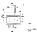
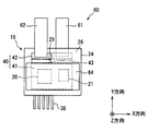
- FIG. 2 is a plan view illustrating a schematic configuration of a power module including the semiconductor device according to the first embodiment.
- FIG. 3 is a sectional view taken along line III-III in FIG.
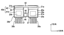
- FIG. 4 is a plan view showing a schematic configuration of the power module according to the second embodiment.
- FIG. 5 is a plan view of the power module as viewed from the back side with respect to FIG.
- FIG. 6 is a plan view in which the sealing resin body is omitted from the semiconductor device in FIG.
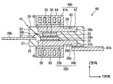
- FIG. 7 is a cross-sectional view taken along line VII-VII in FIG.
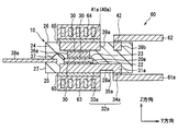
- FIG. 8 is a sectional view taken along line VIII-VIII in FIG.
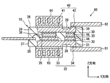
- FIG. 9 is a cross-sectional view illustrating a schematic configuration of a power module including the semiconductor device according to the third embodiment, and corresponds to FIG.
- FIG. 10 is a plan view illustrating a schematic configuration of a power module including the semiconductor device according to the fourth embodiment.
- 11 is a cross-sectional view taken along line XI-XI shown in FIG.
- FIG. 12 is a plan view illustrating a schematic configuration of a power module including the semiconductor device according to the fifth embodiment.
- FIG. 13 is a sectional view taken along line XIII-XIII shown in FIG.
- FIG. 14 is a cross-sectional view showing a first modification, corresponding to FIG.
- FIG. 15 is a plan view showing a second modification, and corresponds to FIG.
- symbol shall be provided to a common thru
- the thickness direction of the semiconductor chip is indicated as the Z direction
- one direction orthogonal to the Z direction is indicated as the X direction
- the direction perpendicular to both the Z direction and the X direction is indicated as the Y direction.
- the XY plane defined by the X direction and the Y direction described above is a plane orthogonal to the Z direction, and unless otherwise specified, the shape along the XY plane is a planar shape.
- the power converter 100 shown in FIG. 1 is configured to convert a DC voltage supplied from a DC power supply 101 into a three-phase AC and output it to a three-phase AC motor 102.
- a power conversion device 100 is mounted on, for example, an electric vehicle or a hybrid vehicle.
- the power conversion device 100 can also convert the power generated by the motor 102 into direct current and charge the direct current power source 101 (battery).
- Reference numeral 103 shown in FIG. 2 is a smoothing capacitor.
- the power converter 100 has a three-phase inverter.
- the three-phase inverter is a three-phase circuit provided between a high potential power line 104 connected to the positive electrode (high potential side) of the DC power source 101 and a low potential power line 105 connected to the negative electrode (low potential side).
- each of the six arms is constituted by the semiconductor device 10.
- the semiconductor device 10 includes an IGBT element and a freewheeling wheel FWD (Free wheel diode) element connected in reverse parallel to the IGBT element.
- FWD Free wheel diode
- an n-channel IGBT element is employed.
- the cathode electrode of the FWD element is shared with the collector electrode, and the anode electrode is shared with the emitter electrode.
- the collector electrode of the IGBT element on the upper arm side is electrically connected to the high potential power supply line 104, and the emitter electrode is connected to the corresponding three-phase line 106 of the motor 102.
- the collector electrode of the IGBT element on the lower arm side is connected to the corresponding three-phase line 106 of the motor 102, and the emitter electrode is electrically connected to the low potential power supply line 105.
- the power conversion device 100 includes a boost converter that boosts a DC voltage supplied from the DC power supply 101, and a control unit that controls the operation of the switching elements constituting the three-phase inverter and the boost converter. You may have.
- the semiconductor device 10 is known as a so-called 1 in 1 package.
- the semiconductor device 10 includes two semiconductor chips 20 and 21.
- the semiconductor chip 20 is formed by forming an IGBT element as an element on a semiconductor substrate such as silicon.
- the semiconductor chip 21 is formed by forming an FWD element as an element on a semiconductor substrate.
- the semiconductor chips 20 and 21 correspond to the semiconductor chip of the present disclosure. Note that the IGBT element and the FWD element may be formed on the same semiconductor chip.
- These semiconductor chips 20 and 21 are arranged side by side in the X direction and are arranged at substantially the same position in the Z direction. Further, the planar shapes of the semiconductor chips 20 and 21 are both substantially rectangular.
- the semiconductor chips 20 and 21 have a first main surface 22 and a second main surface 23 opposite to the first main surface 22 as surfaces orthogonal to the Z direction. Both the IGBT element and the FWD element have a so-called vertical structure so that a current flows in the Z direction.
- the semiconductor chip 20 has a collector electrode as a first main electrode on the first main surface 22 side, and an emitter electrode as a second main electrode on the second main surface 23. In addition to the emitter electrode, a pad for a gate electrode or the like is formed on the second main surface 23.
- the semiconductor chip 21 has a cathode electrode as the first main electrode on the first main surface 22 side, and an anode electrode as the second main electrode on the second main surface 23.
- the sealing resin body 24 is made of, for example, an epoxy resin.
- the sealing resin body 24 has a substantially rectangular planar shape, and includes a surface 25 orthogonal to the Z direction, a back surface 26 opposite to the surface 25, and a side surface 27 that connects the surface 25 and the back surface 26. Yes.
- the one surface 25 and the back surface 26 are flat surfaces.
- the one surface 25 corresponds to the first surface, and the back surface 26 corresponds to the second surface.
- the sealing resin body 24 has insulating separation portions 28 and 29. Details of the insulating separation portions 28 and 29 will be described later.
- the collector electrode is formed on almost the entire first main surface 22.
- the collector electrode is electrically, thermally, and mechanically connected to the first heat sink 31 via the solder 30.
- the cathode electrode is also electrically, thermally and mechanically connected to the first heat sink 31 via a solder (not shown).
- the first heat sink 31 has a function of radiating heat generated by the semiconductor chips 20 and 21 to the outside of the semiconductor device 10 and a function of electrically relaying the semiconductor chips 20 and 21 and a first bus bar 61 described later.
- the first heat sink 31 is formed using at least a metal material in order to ensure thermal conductivity and electrical conductivity. For example, it consists of metal materials excellent in thermal conductivity and electrical conductivity, such as copper, copper alloy, and aluminum alloy.
- a region facing the semiconductor chips 20 and 21 where the solder 30 is not disposed and a side surface are covered with a sealing resin body 24.
- the surface opposite to the facing surface is an exposed surface 32 exposed from one surface 25 of the sealing resin body 24.
- the exposed surface 32 is substantially flush with the one surface 25 of the sealing resin body 24.
- the exposed surface 32 of the first heat sink 31 has a heat dissipation area 33 and an electrical connection area 34.
- a groove portion 35 is formed in the first heat sink 31, and the exposed surface 32 is divided into two in the Y direction by the groove portion 35.
- the groove portion 35 is formed from one end of the first heat sink 31 to the other end along the X direction.
- the exposed surface 32 is partitioned into a heat dissipation region 33 and an electrical connection region 34. Both the heat dissipation area 33 and the electrical connection area 34 have a planar rectangular shape.
- the heat dissipation area 33 includes an area overlapping with the semiconductor chips 20 and 21 when viewed from the Z direction. In other words, it is set so as to overlap the semiconductor chips 20 and 21 in a coordinate system (XY coordinate system) orthogonal to the Z direction. And the 1st cooler 63 mentioned later is thermally connected to the thermal radiation area
- the electrical connection region 34 is a portion of the exposed surface 32 excluding the heat dissipation region 33.
- the electrical connection region 34 is a region that does not overlap the semiconductor chips 20 and 21 when viewed from the Z direction. In other words, the coordinate system orthogonal to the Z direction is set so as not to overlap the semiconductor chips 20 and 21.
- the first bus bar 61 is electrically connected to the electrical connection region 34 by welding or the like.
- the electrical connection region 34 of the exposed surface 32 contributes to electrical connection (relay) between the semiconductor chips 20 and 21 and the first bus bar 61.
- the electrical connection region 34 is located farther than the heat dissipation region 33 with respect to the surface of the side surface 27 of the sealing resin body 24 from which a signal terminal 38 to be described later projects.
- the heat radiation area 33 is large.
- the electrical connection region 34 only needs to ensure the connection with the first bus bar 61. For this reason, the area of the heat dissipation region 33 is larger than the area of the electrical connection region 34.
- the sealing resin body 24 is disposed in the groove portion 35 of the first heat sink 31, and the insulating separation portion 28 by the sealing resin body 24 is configured.
- the insulating separation part 28 is connected to the other part of the sealing resin body 24.
- the surface of the insulating separation portion 28 is also substantially flush with the exposed surface 32, as is the case with other portions of the one surface 25 of the sealing resin body 24.
- the emitter electrode is formed on a part of the second main surface 23.
- the emitter electrode is electrically, thermally and mechanically connected to the terminal 36 via the solder 30. Since the terminal 36 is located in the middle of the heat conduction and electric conduction paths between the second heat sink 39 and the semiconductor chips 20 and 21 to be described later, at least a metal material is used to ensure the heat conductivity and the electric conductivity. Is formed. For example, it is made of a metal material having excellent thermal conductivity and electrical conductivity such as copper and molybdenum.
- the anode electrode of the semiconductor chip 21 is also electrically, thermally, and mechanically connected to the terminal via solder.
- a pad for external connection (not shown) is formed on the second main surface 23 of the semiconductor chip 20 in a part of the outer peripheral region excluding the emitter electrode formation region.
- the pad is not only for the gate electrode, but also for the Kelvin emitter that detects the potential of the emitter electrode, for the anode potential of the temperature-sensitive diode that detects the temperature of the semiconductor element, and also for the cathode potential and the current sense. Is formed.
- a signal terminal 38 is electrically connected to the pad via a bonding wire 37. As shown in FIG. 2, the signal terminal 38 extends in the Y direction. A part thereof protrudes from one of the side surfaces 27 of the sealing resin body 24 to the outside.
- the signal terminal 38 can be electrically connected to an external device.
- the side surface 27 from which the signal terminal 38 protrudes is a surface (ZX surface) orthogonal to the arrangement direction of the heat dissipation region 33 and the electrical connection region 34 and is a surface on the heat dissipation region 33 side.
- a second heat sink 39 is electrically, thermally, and mechanically connected to the surface of the terminal 36 opposite to the semiconductor chip 20 via the solder 30.
- the terminal on the semiconductor chip 21 side is also electrically, thermally and mechanically connected to the second heat sink 39 via solder.
- the second heat sink 39 has a function of radiating heat generated by the semiconductor chips 20 and 21 to the outside of the semiconductor device 10 and a function of electrically relaying the semiconductor chips 20 and 21 and a second bus bar 62 described later.
- the second heat sink 39 has the same configuration as the first heat sink 31.
- the second heat sink 39 is provided so that most of the second heat sink 39 overlaps with the first heat sink 31 when viewed from the Z direction.
- the second heat sink 39 may be configured to substantially coincide with the first heat sink 31.
- the second heat sink 39 is formed by using at least a metal material in order to ensure thermal conductivity and electrical conductivity.
- the region on the semiconductor chip 20, 21 side where the solder 30 is not disposed and the side surface are covered with the sealing resin body 24.
- the surface opposite to the surface on the semiconductor chip 20, 21 side is an exposed surface 40 exposed from the back surface 26 of the sealing resin body 24. The exposed surface 40 is substantially flush with the back surface 26.
- the exposed surface 40 of the second heat sink 39 also has a heat radiation region 41 and an electrical connection region 42.
- the exposed surface 40 is divided into two in the Y direction by the groove 43.
- the groove 43 is formed from one end of the second heat sink 39 to the other end along the X direction.
- the exposed surface 40 is partitioned into a heat dissipation area 41 and an electrical connection area 42. Both the heat radiation area 41 and the electrical connection area 42 have a planar rectangular shape.
- the heat radiation area 41 includes an area overlapping with the semiconductor chips 20 and 21 in the projection view from the Z direction. In other words, it is set so as to overlap with the semiconductor chips 20 and 21 in a coordinate system orthogonal to the Z direction. In the present embodiment, the heat radiation area 41 substantially coincides with the heat radiation area 33 in the projection view from the Z direction. A second cooler 64 described later is thermally connected to the heat radiation area 41. Therefore, in the exposed surface 40, the heat dissipation area 41 contributes to heat dissipation of the semiconductor chips 20 and 21.
- the electrical connection region 42 is a portion of the exposed surface 40 excluding the heat dissipation region 41.
- the electrical connection region 42 is a region that does not overlap the semiconductor chips 20 and 21 in the projection view from the Z direction. In other words, the coordinate system orthogonal to the Z direction is set so as not to overlap the semiconductor chips 20 and 21.
- the second bus bar 62 is electrically connected to the electrical connection region 42 by welding or the like.
- the electrical connection region 42 of the exposed surface 40 contributes to electrical connection (relay) between the semiconductor chips 20 and 21 and the second bus bar 62.
- the electrical connection region 42 in the Y direction, is located farther than the heat radiation region 41 with respect to the surface of the side surface 27 of the sealing resin body 24 from which the signal terminal 38 protrudes. That is, the exposed surface 32 has the same arrangement as the heat radiation area 33 and the electrical connection area 34.
- the electrical connection region 42 and the electrical connection region 34 are in a positional relationship where they overlap each other. In the present embodiment, as an example, the electrical connection regions 34 and 42 substantially coincide with each other.
- the heat radiation area 41 is large.
- the electrical connection region 42 only needs to ensure the connection with the second bus bar 62. For this reason, the area of the heat dissipation region 41 is larger than the area of the electrical connection region 42.
- the sealing resin body 24 is also disposed in the groove 43 of the second heat sink 39, and the insulating separation part 29 is configured by the sealing resin body 24.
- This insulating separation part 29 is also connected to the other part of the sealing resin body 24.
- the surface of the insulating separation portion 29 is substantially flush with the exposed surface 40 as is the case with the other portions of the back surface 26 of the sealing resin body 24.
- the first heat sink 31 and the second heat sink 39 are also referred to as heat sinks 31 and 39.
- the power module 60 includes a first bus bar 61, a second bus bar 62, a first cooler 63, a second cooler 64, and an insulating plate 65.
- first bus bar 61 and the second bus bar 62 are also referred to as bus bars 61 and 62.
- the first cooler 63 and the second cooler 64 are also referred to as coolers 63 and 64.
- the first bus bar 61 and the second bus bar 62 are each formed using a conductive material such as copper, and are electrically connected to the electrical connection regions 34 and 42 of the corresponding heat sinks 31 and 39 by welding or the like.
- the first bus bar 61 connected to the electrical connection region 34 of the first heat sink 31 constitutes at least a part of the high potential power supply line 104.
- the positive electrode side of the smoothing capacitor 103 and the collector electrode of the semiconductor chip 20 and the cathode electrode of the semiconductor chip 21 are electrically relayed.
- the second bus bar 62 connected to the electrical connection region 42 of the second heat sink 39 constitutes at least a part of the three-phase wire 106.
- the motor 102 and the emitter electrode of the semiconductor chip 20 and the anode electrode of the semiconductor chip 21 are electrically relayed.
- the first bus bar 61 constitutes at least a part of the three-phase wire 106.
- the second bus bar 62 constitutes at least a part of the low potential power line 105.
- the negative electrode side of the smoothing capacitor 103 and the emitter electrode of the semiconductor chip 20 and the anode electrode of the semiconductor chip 21 are electrically relayed.
- the bus bars 61 and 62 are both flat and have a planar rectangular shape whose longitudinal direction is the Y direction.
- the bus bars 61 and 62 extend from the corresponding electrical connection regions 34 and 42 to the outside of the semiconductor device 10 in the opposite direction to the heat dissipation regions 33 and 41. Further, in the projection view from the Z direction, the first bus bar 61 and the second bus bar 62 are in a positional relationship where they overlap each other.
- the first cooler 63 and the second cooler 64 for example, a refrigerant is circulated inside, and a general one that effectively dissipates heat from the semiconductor device 10 can be adopted.
- the first cooler 63 is disposed corresponding to the heat radiation area 33 of the first heat sink 31.
- the second cooler 64 is disposed corresponding to the heat radiation area 41 of the second heat sink 39.
- Insulating plates 65 are interposed between the coolers 63 and 64 and the corresponding heat radiation regions 33 and 41, respectively.
- the insulating plate 65 has an insulating property for electrically insulating the semiconductor device 10 and the coolers 63 and 64, and has a thermal conductivity for transferring heat from the semiconductor device 10 to the coolers 63 and 64. Yes.
- Such an insulating plate 65 is formed using ceramics such as silicon nitride and alumina, and has a predetermined thickness in order to ensure the above-described insulation and thermal conductivity.
- the insulating plate 65 is disposed on the one surface 25 side in the Z direction so as to face the heat radiation region 33 of the exposed surface 32 of the first heat sink 31. Further, another insulating plate 65 is arranged on the back surface 26 side in the Z direction so as to face the heat radiation area 41 of the exposed surface 40 of the second heat sink 39. The insulating plate 65 is fixed to the corresponding heat radiation regions 33 and 41 and the coolers 63 and 64 through, for example, silicone grease.
- an insulating separation part 28 made of the sealing resin body 24 is interposed between the first bus bar 61 and the first cooler 63. That is, there is a gap between the first bus bar 61 and the first cooler 63 in the Y direction. Further, an insulating separation part 29 made of the sealing resin body 24 is interposed between the second bus bar 62 and the second cooler 64. That is, a gap exists between the second bus bar 62 and the second cooler 64 in the Y direction.
- the semiconductor chips 20 and 21, the heat sinks 31 and 39, the terminal 36, and the signal terminal 38 are prepared. At this time, the heat sinks 31 and 39 having the grooves 35 and 43 are prepared.
- connection step before molding the sealing resin body 24 is performed.
- the first heat sink 31 and the semiconductor chips 20 and 21 are connected via the solder 30.
- the semiconductor chips 20 and 21 and the terminal 36 are connected via the solder 30.
- the signal terminal 38 and the pad of the semiconductor chip 20 are connected by the bonding wire 37.
- the terminal 36 and the second heat sink 39 are connected via the solder 30.
- the structure formed through the above connection process is placed in a mold (not shown), and resin is injected into the cavity of the mold to mold the sealing resin body 24.
- the sealing resin body 24 is molded by a transfer molding method using an epoxy resin.
- the sealing resin body 24 is molded so that the heat sinks 31 and 39 are completely covered.
- a cutting process is performed.
- the sealing resin body 24 is pressed from both sides in the X direction while the side surface 27 of the sealing resin body 24 is vacuum chucked by a pressing jig (not shown).
- a pressing jig not shown
- the one surface 25 side of the sealing resin body 24 is cut together with the first heat sink 31.
- the back surface 26 side is cut together with the second heat sink 39.
- the exposed surfaces 32 and 40 of the heat sinks 31 and 39 are exposed from the sealing resin body 24 by this cutting.
- the exposed surface 32 is substantially flush with the surrounding surface 25, and the exposed surface 40 is substantially flush with the surrounding back surface 26. Since the cutting is performed at a position shallower than the bottom of the groove portions 35 and 43, the groove portions 35 and 43 and the insulating separation portions 28 and 29 remain even after the cutting.
- the heat sinks 31 and 39 formed using a metal material and the sealing resin body 24 are different in hardness from the constituent materials, so that there is a slight difference in the amount of cutting. 25, and between the exposed surface 40 and the back surface 26, steps of several ⁇ m or less (for example, 2 ⁇ m or less) are generated. However, it is several ⁇ m or less, and it is assumed that such an extremely minute step is substantially flush.
- the semiconductor device 10 can be obtained through cutting of a tie bar (not shown) in the lead frame.
- the coolers 63 and 64 are thermally connected to the heat radiation regions 33 and 41 on the exposed surfaces 32 and 40 of the heat sinks 31 and 39, respectively. Therefore, the heat of the semiconductor chips 20 and 21 can be released to both sides of the semiconductor device 10.
- bus bars 61 and 62 are electrically connected to the electrical connection regions 34 and 42 on the exposed surfaces 32 and 40 of the heat sinks 31 and 39, respectively. In this way, the bus bars 61 and 62 are connected to the heat sinks 31 and 39 without going through external connection terminals (outer leads). Since there is no terminal for external connection, an increase in inductance due to a thin terminal can be suppressed. That is, the surge voltage generated at the time of switching can be suppressed.
- the electrical connection region 34 of the exposed surface 32 and the electrical connection region 42 of the exposed surface 40 are in a positional relationship where they overlap each other in the projection view from the Z direction.
- the first bus bar 61 connected to the electrical connection region 34 and the second bus bar 62 connected to the electrical connection region 42 also have a positional relationship that overlaps each other in the projected view from the Z direction. Since the first bus bar 61 and the second bus bar 62 flow in opposite directions, the effect of canceling the magnetic fluxes can be enhanced. Thereby, parasitic inductance can be reduced. That is, the surge voltage generated at the time of switching can be more effectively suppressed.
- the heat radiation area 33 and the electrical connection area 34 are separated by the sealing resin body 24. Accordingly, the first bus bar 61 and the first cooling are compared with a configuration in which the sealing resin body 24 is not disposed between the heat dissipation region 33 and the electrical connection region 34, for example, a configuration in which the heat dissipation region 33 and the electrical connection region 34 are continuous.
- the creepage distance of the vessel 63 can be earned.
- the contact (short circuit) of the 1st bus-bar 61 and the 1st cooler 63 can be suppressed.
- the heat radiation area 41 and the electrical connection area 42 are separated by the sealing resin body 24. The effect is the same as above.
- the first heat sink 31 has a groove 35 between the heat dissipation region 33 and the electrical connection region 34, and the sealing resin body 24 is disposed in the groove 35 to form the insulating separation portion 28.
- the second heat sink 39 has a groove portion 43 between the heat radiation region 41 and the electrical connection region 42, and the sealing resin body 24 is disposed in the groove portion 43 to form the insulating separation portion 29.
- the heat radiation regions 33 and 41 and the electrical connection regions 34 and 42 are separated by the insulating separation portions 28 and 29 of the sealing resin body 24.
- the exposed surfaces 32 and 40 are exposed by cutting the sealing resin body 24 after molding, but by adopting this method, a new process is not added.
- the heat radiation areas 33 and 41 and the electrical connection areas 34 and 42 can be separated. Therefore, the manufacturing process can be simplified.
- the exposed surfaces 32 and 40 may be exposed without being cut.
- the sealing resin body 24 may be molded in a state where the exposed surfaces 32 and 40 of the heat sinks 31 and 39 are pressed against and adhered to the cavity wall surface of the mold.
- the exposed surfaces 32 and 40 are exposed from the sealing resin body 24 when the sealing resin body 24 is molded. Insulation separation portions 28 and 29 are also formed. According to this, it is possible to simplify the manufacturing process by eliminating the cutting process while simplifying the mold shape.
- the semiconductor device 10 has only one arm out of the six arms constituting the three-phase inverter. That is, in the first embodiment, the semiconductor device 10 having a 1 in 1 package structure is shown. In contrast, the present embodiment is different in that the semiconductor device 10 has a 2-in-1 package structure as shown in FIGS. 4, 5, 6, 7, and 8. That is, the semiconductor device 10 has upper and lower arms for one phase of the three phases.
- the semiconductor device 10 includes semiconductor chips 20a and 20b, a sealing resin body 24, first heat sinks 31a and 31b, terminals 36a and 36b, signal terminals 38a and 38b, and second heat sinks 39a and 39b.
- the semiconductor chips 20 a and 20 b correspond to the semiconductor chip 20 described in the first embodiment, and the first heat sinks 31 a and 31 b correspond to the first heat sink 31.
- the terminals 36 a and 36 b correspond to the terminal 36, and the signal terminals 38 a and 38 b correspond to the signal terminal 38.
- the second heat sinks 39 a and 39 b correspond to the second heat sink 39.
- the semiconductor chip 20a includes an upper arm side IGBT element and an FWD element
- the semiconductor chip 20b includes a lower arm side IGBT element and an FWD element.
- the IGBT element and the FWD element may be formed on different semiconductor chips.
- These semiconductor chips 20a and 20b have substantially the same shape.
- the semiconductor chips 20a and 20b are arranged side by side in the X direction and are arranged at substantially the same position in the Z direction.
- the semiconductor chips 20a and 20b have a collector electrode (also a cathode electrode) as a first main electrode on the first main surface 22 side, and an emitter electrode (also an anode electrode) as a second main electrode on the second main surface 23 side. )have.
- the collector electrode is formed on almost the entire first main surface 22.
- the collector electrode of the semiconductor chip 20a is electrically, thermally, and mechanically connected to the first heat sink 31a via the solder 30.
- the collector electrode of the semiconductor chip 20b is electrically, thermally and mechanically connected to the first heat sink 31b via the solder 30.
- the first heat sink 31a has a function of radiating heat generated by the semiconductor chip 20a to the outside of the semiconductor device 10 and a function of electrically relaying the semiconductor chip 20a and a first bus bar 61a described later.
- the surface opposite to the surface facing the semiconductor chip 20 a is an exposed surface 32 a exposed from the one surface 25 of the sealing resin body 24.
- the exposed surface 32 a is substantially flush with the one surface 25 of the sealing resin body 24.
- the first heat sink 31b has a function of radiating heat generated by the semiconductor chip 20b to the outside of the semiconductor device 10 and a function of electrically relaying the semiconductor chip 20b and a first bus bar 61b described later.
- the surface opposite to the surface facing the semiconductor chip 20 b is an exposed surface 32 b exposed from the one surface 25 of the sealing resin body 24.
- the exposed surface 32 b is also substantially flush with the one surface 25 of the sealing resin body 24.
- the exposed surface 32a of the first heat sink 31a has a heat dissipation area 33a and an electrical connection area 34a.
- a groove 35a is formed in the first heat sink 31, and the exposed surface 32a is divided into two in the Y direction by the groove 35a.
- the groove 35a is formed from one end of the first heat sink 31a to the other end along the X direction.
- the exposed surface 32a is partitioned into a heat dissipation region 33a and an electrical connection region 34a.
- the exposed surface 32b of the first heat sink 31b also has a heat dissipation area 33b and an electrical connection area 34b.
- a groove portion 35 b is formed in the first heat sink 31.
- the groove 35b is formed from one end to the other end of the first heat sink 31b along the X direction. By the groove 35b, the exposed surface 32b is partitioned into a heat dissipation region 33b and an electrical connection region 34b.
- the heat radiation area 33a is set so as to overlap with the semiconductor chip 20a in the projection view from the Z direction.
- the 1st cooler 63 is thermally connected to the thermal radiation area
- the heat radiation area 33b is set so as to overlap the semiconductor chip 20b when viewed from the Z direction.
- the 1st cooler 63 is thermally connected to the thermal radiation area
- the heat radiation areas 33a and 33b are substantially the same position in the Y direction and are arranged side by side in the X direction.
- the electrical connection region 34a is a portion of the exposed surface 32a excluding the heat dissipation region 33a.
- the electrical connection region 34a is a region that does not overlap the semiconductor chip 20a when viewed from the Z direction.
- the first bus bar 61a is electrically connected to the electrical connection region 34a.
- the electrical connection region 34a is located farther than the heat dissipation region 33a with respect to the surface of the side surface 27 of the sealing resin body 24 from which a signal terminal 38a to be described later projects.
- the electrical connection region 34b is a portion of the exposed surface 32b excluding the heat dissipation region 33b.
- the electrical connection region 34b is a region that does not overlap the semiconductor chip 20b in the projection view from the Z direction.
- the first bus bar 61b is electrically connected to the electrical connection region 34b.
- the electrical connection region 34b is located farther than the heat radiation region 33b with respect to the surface of the side surface 27 of the sealing resin body 24 from which a signal terminal 38b to be described later projects.
- the electrical connection areas 34a and 34b are substantially the same position in the Y direction and are arranged side by side in the X direction.
- the sealing resin bodies 24 are respectively disposed in the groove portions 35a and 35b of the first heat sinks 31a and 31b, and the insulating separation portions 28a and 28b by the sealing resin body 24 are configured.
- the surfaces of the insulating separation portions 28a and 28b are substantially flush with the exposed surfaces 32a and 32b, as with other portions of the one surface 25 of the sealing resin body 24.
- the emitter electrode is formed on a part of each second main surface 23.
- the emitter electrode of the semiconductor chip 20 a is electrically, thermally, and mechanically connected to the terminal 36 a through the solder 30.
- the emitter electrode of the semiconductor chip 20b is electrically, thermally, and mechanically connected to the terminal 36b through the solder 30.
- a signal terminal 38 a is electrically connected to the pad of the semiconductor chip 20 a via a bonding wire 37.
- the signal terminal 38a extends in the Y direction. A part thereof protrudes from one of the side surfaces 27 of the sealing resin body 24 to the outside.
- the signal terminal 38b is electrically connected to the pad of the semiconductor chip 20b through the bonding wire 37.
- the signal terminal 38b is also extended in the Y direction. A part of the side surface 27 of the sealing resin body 24 protrudes to the outside from the same surface as the surface from which the signal terminal 38 a protrudes.
- a second heat sink 39a is electrically, thermally, and mechanically connected to the surface of the terminal 36a opposite to the semiconductor chip 20a through the solder 30.
- the second heat sink 39b is electrically, thermally, and mechanically connected to the surface of the terminal 36b opposite to the semiconductor chip 20b via the solder 30.
- the second heat sink 39a functions to radiate the heat generated by the semiconductor chip 20a to the outside of the semiconductor device 10.
- the second heat sink 39a is provided so as to overlap the first heat sink 31a in the projection view from the Z direction.
- the second bus bar 62 is not connected to the second heat sink 39a.
- the second heat sink 39b has a function of radiating heat generated by the semiconductor chip 20b to the outside of the semiconductor device 10 and a function of electrically relaying the semiconductor chip 20b and the second bus bar 62.
- the second heat sink 39b is provided so as to overlap the first heat sink 31b in the projection view from the Z direction.
- the surface opposite to the surface on the semiconductor chip 20a side is an exposed surface 40a exposed from the back surface 26 of the sealing resin body 24.
- the exposed surface 40a is substantially flush with the back surface 26.
- the second heat sink 39a has only the heat radiation area 41a as the exposed surface 40a. That is, it does not have an electrical connection area.
- the surface opposite to the surface on the semiconductor chip 20b side is an exposed surface 40b exposed from the back surface 26 of the sealing resin body 24.
- the exposed surface 40b is also substantially flush with the back surface 26.
- the second heat sink 39b has a heat radiation area 41b and an electrical connection area 42b as the exposed surface 40b.
- the exposed surface 40 b is divided into two in the Y direction by the groove 43.
- the groove 43 is formed from one end of the second heat sink 39b to the other end along the X direction.
- the exposed surface 40b is partitioned into a heat dissipation area 41b and an electrical connection area 42b. Both the heat radiation area 41b and the electrical connection area 42b have a planar rectangular shape.
- the electrical connection region 42b extends in the X direction.
- the heat radiation area 41a is set so as to overlap the semiconductor chip 20a in the projection view from the Z direction. In the present embodiment, the heat radiation area 41a substantially coincides with the heat radiation area 33a in the projection view from the Z direction.
- the second cooler 64 is thermally connected to the heat radiation area 41a.
- the heat radiation area 41b is set so as to overlap the semiconductor chip 20b in the projection view from the Z direction. In the present embodiment, the heat radiation area 41b substantially coincides with the heat radiation area 33b in the projection view from the Z direction.
- the second cooler 64 is also thermally connected to the heat radiation area 41b.
- the heat radiation regions 41a and 41b are substantially the same position in the Y direction and are arranged side by side in the X direction.
- the electrical connection region 42 is a region that does not overlap with the semiconductor chip 20b when viewed from the Z direction.
- the second bus bar 62 is electrically connected to the electrical connection region 42.
- the electrical connection region 42b extends in the X direction. Specifically, it extends to a position overlapping the electrical connection region 34a in the coordinate system orthogonal to the Z direction.
- the sealing resin body 24 is also disposed in the groove portion 43 of the second heat sink 39b, and the insulating separation portion 29 is configured by the sealing resin body 24.
- the surface of the insulating separation portion 29 is substantially flush with the exposed surface 40 as is the case with the other portions of the back surface 26 of the sealing resin body 24.
- the semiconductor device 10 has joint portions 44 and 45 as shown in FIG.
- the joint portion 44 extends from the first heat sink 31b in the X direction and toward the first heat sink 31a.
- the joint portion 45 extends from the second heat sink 39a in the X direction and toward the second heat sink 39b.
- the joint portions 44 and 45 are electrically and mechanically connected by solder (not shown).
- the entire joint portions 44 and 45 are covered with the sealing resin body 24. It is also possible to adopt a configuration in which the joint portion is formed on only one of the first heat sink 31b and the second heat sink 39a. Since such a joint structure for connecting the upper arm and the lower arm is well known, detailed description thereof will be omitted.
- the power module 60 includes first bus bars 61 a and 61 b, a second bus bar 62, a first cooler 63, a second cooler 64, and an insulating plate 65.
- the first bus bars 61a and 61b correspond to the first bus bar 61 of the first embodiment.
- the first bus bars 61a and 61b are also referred to as bus bars 61a and 61b.
- the first bus bar 61 a constitutes at least a part of the high potential power supply line 104.
- the first bus bar 61a is connected to the electrical connection region 34a of the first heat sink 31a.
- the first bus bar 61 b constitutes at least a part of the three-phase line 106.
- the first bus bar 61b is connected to the electrical connection region 34b of the first heat sink 31b.
- the first bus bars 61a and 61b are both disposed on the one surface 25 side of the sealing resin body 24.
- the first bus bars 61a and 61b are both flat and have a planar rectangular shape with the Y direction as the longitudinal direction.
- the bus bars 61a and 61b extend from the corresponding electrical connection regions 34a and 34b to the outside of the semiconductor device 10 in the direction opposite to the heat dissipation regions 33a and 33b. That is, the first bus bars 61a and 61b have the same longitudinal direction and are arranged side by side in the X direction.
- the second bus bar 62 constitutes at least a part of the low potential power line 105.
- the second bus bar 62 is connected to the electrical connection region 42 of the second heat sink 39b.
- the second bus bar 62 is disposed on the back surface 26 side of the sealing resin body 24.
- the second bus bar 62 is a flat plate and has a planar rectangular shape with the Y direction as the longitudinal direction.
- the bus bar 62 extends from the electrical connection region 42 to the outside of the semiconductor device 10 in the direction opposite to the heat dissipation region 41b. Further, the bus bar 62 is connected to a portion of the electrical connection region 42 that overlaps with the electrical connection region 34a in the projection view from the Z direction. That is, in the projection view from the Z direction, the first bus bar 61a and the second bus bar 62 overlap each other.
- the 1st cooler 63 is arrange
- FIG. The second cooler 64 is disposed on the heat radiation areas 41a and 41b via the insulating plate 65.
- an insulating separation part 28a is interposed between the first bus bar 61a and the first cooler 63.
- an insulation separator 28b is interposed between the first bus bar 61b and the first cooler 63.
- an insulating separation part 29 is interposed between the second bus bar 62 and the second cooler 64.
- the semiconductor device 10 having the 2-in-1 package structure configured as described above and the power module 60 including the semiconductor device 10 can also achieve the same effects as those described in the first embodiment.
- the heat sink connected to the bus bar has a heat dissipation area and an electrical connection area as an exposed surface.
- the bus bars 61a, 61b, 62 are connected only to the first heat sinks 31a, 31b and the second heat sink 39b among the first heat sinks 31a, 31b and the second heat sinks 39a, 39b.
- the second heat sink 39a has only the heat radiation area 41a as the exposed surface 40a.
- bus bar which comprises the three-phase wire 106 should just be connected to at least one of the 1st heat sink 31b and the 2nd heat sink 39a.
- the first bus bar 61b constituting the three-phase wire 106 is connected only to the first heat sink 31b. Since the second heat sink 39a does not have an electrical connection area, the electrical connection area 42 of the second heat sink 39b is extended to an empty space. Thereby, the electrical connection area
- the effect of canceling the magnetic fluxes with each other is obtained. It can be further increased.
- the effect of canceling out the magnetic fluxes can be enhanced as compared with a configuration in which the bus bar forming the high-potential power supply line 104 and the bus bar forming the three-phase line 106 are in an overlapping positional relationship.
- the effect of canceling the magnetic fluxes can be enhanced as compared with the configuration in which the bus bar forming the low-potential power supply line 105 and the bus bar forming the three-phase line 106 have an overlapping positional relationship.
- the first bus bar 61b constituting the three-phase line 106 and the second bus bar 62 constituting the low-potential power line 105 overlap can be employed.
- the second heat sink 39a may have an electrical connection region as the exposed surface 40a, and a bus bar constituting the three-phase wire 106 may be connected to the electrical connection region.
- the present embodiment is characterized in that at least one of the bus bars 61 and 62 is bent. Below, an example of a bending structure is shown.
- both the first bus bar 61 and the second bus bar 62 are bent.
- the first bus bar 61 has a bent portion 61 c outside the semiconductor device 10 in the Y direction which is the extending direction of the first bus bar 61.
- the first flat plate portion 61d and the second flat plate portion 61e are connected by the bent portion 61c.
- the first flat plate portion 61d is a flat plate-like portion extending in the Y direction, with its own plate thickness direction being the Z direction.
- the second flat plate portion 61e is also a flat plate portion extending in the Y direction with its own plate thickness direction being the Z direction.
- the bent portion 61c has a first bent portion 61c1, a second bent portion 61c2, and a connecting portion 61c3.
- the first bus bar 61 is bent at the first bent portion 61c1.
- the connecting portion 61c3 is inclined and extended with respect to the Y direction on the side closer to the back surface 26.
- the first bus bar 61 is bent at the second bent portion 61c2.
- the 2nd flat plate part 61e is extended in the Y direction. That is, the first flat plate portion 61d and the second flat plate portion 61e are substantially parallel to each other.
- the second bus bar 62 has a bent portion 62c outside the semiconductor device 10 in the Y direction which is the extending direction of the second bus bar 62.
- the first flat plate portion 62d and the second flat plate portion 62e are connected by the bent portion 62c.
- the first flat plate portion 62d is a flat plate-like portion extending in the Y direction with the plate thickness direction of the first flat plate portion 62d being the Z direction.
- the second flat plate portion 62e is also a flat plate-like portion extending in the Y direction with its own plate thickness direction being the Z direction.
- the bent portion 62c has a first bent portion 62c1, a second bent portion 62c2, and a connecting portion 62c3.
- the second bus bar 62 is bent at the first bent portion 62c1.
- the connecting part 62c3 is inclined and extended with respect to the Y direction on the side approaching the one surface 25.
- the second bus bar 62 is bent at the second bent portion 62c2.
- the second flat plate portion 62e extends in the Y direction. That is, the first flat plate portion 62d and the second flat plate portion 62e are substantially parallel to each other.
- the opposing distance (distance in the Z direction) between the first bus bar 61 and the second bus bar 62 is outside the semiconductor device 10 with the semiconductor device 10. It is narrower than the overlapping position. Specifically, the facing distance between the second flat plate portions 61e and 62e is narrower than the facing distance between the first flat plate portions 61d and 62d.
- first bus bar 61 and the second bus bar 62 are bent.
- the Z direction can be obtained. You may make it approach in.
- the bent shape is not limited to the above example.
- the configuration shown in the present embodiment can be applied to the configuration shown in the second embodiment.
- the semiconductor device 10 is interposed between the first heat sink 31 and the second heat sink 39 so as to correspond to the electrical connection regions 34 and 42, and is connected to the heat sinks 31 and 39. It is characterized by further comprising a spacer for electrically separating the second heat sink 39. Below, an example of a spacer is shown.
- the semiconductor device 10 shown in FIGS. 10 and 11 has dummy chips 46 and 47 and a dummy terminal 48 as elements constituting the spacer.
- the dummy chip 46 is formed by forming a dummy element for electrically separating the first heat sink 31 and the second heat sink 39 on a semiconductor substrate such as silicon.
- the thickness of the dummy chip 46 is substantially the same as that of the semiconductor chip 20.
- the dummy chip 46 is arranged side by side with the semiconductor chip 20 in the Y direction, and is arranged so as to overlap with the electrical connection regions 34 and 42 in the projection view from the Z direction.
- the dummy chip 47 is also formed by forming a dummy element for electrically separating the first heat sink 31 and the second heat sink 39 on the semiconductor substrate.
- the thickness of the dummy chip 47 is substantially the same as that of the semiconductor chip 21.
- the dummy chip 47 is arranged side by side with the semiconductor chip 21 in the Y direction, and is arranged so as to overlap with the electrical connection regions 34 and 42 in the projection view from the Z direction. That is, the dummy chips 46 and 47 are arranged side by side in the X direction.
- An electrode (not shown) is formed on the first main surface 22 side of the dummy chip 46, and this electrode and the first heat sink 31 are connected via the solder 30.
- An electrode (not shown) is also formed on the second main surface side of the dummy chip 46, and this electrode and the dummy terminal 48 are connected via the solder 30.
- the dummy terminal 48 is connected to the second heat sink 39 via the solder 30. Therefore, the dummy chip 46 and the dummy terminal 48 are interposed between the first heat sink 31 and the second heat sink 39.
- an electrode is formed on the first main surface 22 side of the dummy chip 47, and this electrode and the first heat sink 31 are connected via a solder 30.
- An electrode is also formed on the second main surface side of the dummy chip 47, and this electrode and the dummy terminal 48 are connected via the solder 30.
- the dummy terminal 48 is connected to the second heat sink 39 via the solder 30. Therefore, the dummy chip 47 and the dummy terminal 48 are interposed between the first heat sink 31 and the second heat sink 39.
- the spacer including the dummy chips 46 and 47 and the dummy terminal 48 is interposed between the heat sinks 31 and 39, at the time of reflowing the solder 30 in the manufacturing process of the semiconductor device 10, at least one of the heat sinks 31 and 39 is provided. Inclination can be suppressed.
- the number of connection points between the heat sinks 31 and 39 is increased by the dummy chips 46 and 47 and the dummy terminals 48. Therefore, when the sealing resin body 24 is molded, the heat sinks 31 and 39 are inclined due to the pressure of the resin, thereby suppressing the stress from acting on the semiconductor chips 20 and 21.
- the stress acting on the semiconductor chips 20 and 21 when the bus bars 61 and 62 are connected can be reduced.
- the semiconductor device 10 may include only one dummy chip, or may include three or more dummy chips.
- the spacer is not limited to the dummy chips 46 and 47 and the dummy terminal 48.
- the first heat sink 31 and the second heat sink 39 are electrically separated from each other while being connected to the heat sinks 31 and 39 and interposed between the first heat sink 31 and the second heat sink 39 corresponding to the electrical connection regions 34 and 42. Anything is acceptable.
- the configuration shown in the present embodiment can be applied to the configurations shown in the second embodiment and the third embodiment.
- the present embodiment is characterized in that the exposed surfaces 32 and 40 are divided into heat dissipation regions 33 and 41 and electrical connection regions 34 and 42 by the insulating plate 65.
- the insulating plate 65 has an extending portion 65 a that extends outward from between the heat radiation regions 33 and 41 and the coolers 63 and 64.
- the extending portion 65a extends toward the electrical connection regions 34 and 42 in the direction in which the heat dissipation regions 33 and 41 and the electrical connection regions 34 and 42 are arranged (Y direction).
- a portion of the exposed surface 32 that is exposed from the insulating plate 65 is an electrical connection region 34.
- a portion of the exposed surface 40 that is exposed from the insulating plate 65 is an electrical connection region 42.
- the heat radiation areas 33 and 41 to which the coolers 63 and 64 are connected are separated from the electrical connection areas 34 and 42 to which the bus bars 61 and 62 are connected. can do.
- an insulating plate 65 is provided between the first bus bar 61 and the first cooler 63 on the one surface 25 side of the sealing resin body 24, thereby increasing a creepage distance. Furthermore, contact (short circuit) between the first bus bar 61 and the first cooler 63 can be prevented.
- an insulating plate 65 is provided between the second bus bar 62 and the second cooler 64, whereby a creepage distance can be earned. Furthermore, contact (short circuit) between the second bus bar 62 and the second cooler 64 can be prevented.
- the configuration of the semiconductor device 10 is not limited to the 1 in 1 package structure having only one of the upper and lower arms and the 2 in 1 package structure having an arm for one phase.
- it can be applied to a 6 in 1 package having upper and lower arms for three phases.
- the separation by the sealing resin body 24 is not limited to the above example.
- the heat radiation regions 33 and 41 and the electrical connection regions 34 and 42 are separated by the insulating separation portions 49 and 50 disposed on the exposed surfaces 32 and 40 of the heat sinks 31 and 39. Is done.
- the insulation separation parts 49 and 50 are formed across the corresponding heat sinks 31 and 39 along the X direction.
- the insulating separation portions 49 and 50 are part of the sealing resin body 24.
- the exposed surfaces 32, 32a, and 32b are also called first exposed surfaces, and the exposed surfaces 40, 40a, and 40b are also called second exposed surfaces.
- the insulating separation portions 49 and 50 can be formed by cutting so that the insulating separation portions 49 and 50 remain when the sealing resin body 24 is cut, for example. Further, when the sealing resin body 24 is not cut, the insulating separation portions 49 and 50 can be formed when the sealing resin body 24 is molded by using a mold having a cavity wall surface having a predetermined shape. As described above, when the insulating separating portions 49 and 50 projecting from the heat sinks 31 and 39 are employed, the insulating separating portions 49 and 50 serve as positional displacement stoppers, so that the bus bars 61 and 62, the coolers 63 and 64, and the insulating plate 65 is easy to position. Further, the contact between the bus bars 61 and 62 and the corresponding coolers 63 and 64 can be more effectively suppressed.
- a semiconductor device is a semiconductor device having a double-sided cooling structure in which bus bars as electrical relay members are electrically connected, and coolers are respectively disposed on both sides and cooled.
- the semiconductor chip having the first main electrode of the element on the first main surface and the second main electrode of the element on the second main surface opposite to the first main surface, and the first main electrode in the thickness direction of the semiconductor chip A first side of the semiconductor chip, and a sealing resin body for sealing the semiconductor chip, and having a side surface connecting the first side and the rear side, with one side of the surface side and the back side of the second main surface side, A first heat sink electrically connected to the first main electrode; and a second heat sink disposed on the second main surface side of the semiconductor chip and electrically connected to the second main electrode.
- the first heat sink is exposed on only one of the one surface, the back surface, and the side surface of the sealing resin body, and is an exposed surface on which the surface opposite to the surface on the semiconductor chip side is exposed.
- the exposed surface of the heat sink that is electrically connected to the bus bar is a region that overlaps the semiconductor chip in a projected view from the thickness direction, and a heat dissipation region to which the cooler is thermally connected, and the periphery of the heat dissipation region An electrical connection region to which the bus bar is electrically connected.
- the cooler is thermally connected to the heat radiation area on the exposed surface of each heat sink. Therefore, the heat of the semiconductor chip can be released to both sides.
- the bus bar is electrically connected to the electrical connection area on the exposed surface of each heat sink. In this way, the bus bar is connected to the heat sink without going through an external connection terminal (outer lead). Since there is no terminal for external connection, an increase in inductance due to a thin terminal can be suppressed.
- the electrical connection region of the first heat sink and the electrical connection region of the second heat sink may be in a positional relationship in which they overlap each other when projected from the thickness direction.
- the bus bar connected to the electrical connection region of the first heat sink and the bus bar connected to the electrical connection region of the second heat sink are in a positional relationship in which they overlap each other in a projected view from the thickness direction. Since the bus bar connected to the first heat sink (first main electrode) and the bus bar connected to the second heat sink (second main electrode) are in opposite directions, the effect of canceling out the magnetic fluxes with each other Can be increased. Thereby, parasitic inductance can be reduced.
- the heat dissipation region and the electrical connection region may be separated by a sealing resin body.
- the creeping distance between the cooler and the bus bar can be earned by the sealing resin body located between the heat radiation area and the electrical connection area. Further, the contact between the cooler and the bus bar can be suppressed.
- a power module is disposed with respect to a semiconductor device, a heat dissipation area of an exposed surface of each heat sink, a cooler that cools the semiconductor device, and an electrical connection area of the exposed surface of the first heat sink.
- the first bus bar connected to the second bus bar, the second bus bar connected to the electrical connection region of the exposed surface of the second heat sink, and the heat radiating region of the exposed surface and the cooler are respectively interposed to cool the heat of the semiconductor device.
- the creeping distance between the cooler and the bus bar can be earned by the extending portion of the insulating plate. Further, the contact between the cooler and the bus bar can be suppressed.
Landscapes
- Engineering & Computer Science (AREA)
- Power Engineering (AREA)
- Cooling Or The Like Of Semiconductors Or Solid State Devices (AREA)
- Microelectronics & Electronic Packaging (AREA)
- Inverter Devices (AREA)
- Cooling Or The Like Of Electrical Apparatus (AREA)
Abstract
半導体装置は、バスバー(61,62)が電気的に接続され、冷却器(63,64)が両面側に配置されて冷却される。半導体装置は、第1主電極を第1主面(22)に有し、第2主電極を第2主面(23)に有する半導体チップ(20)と、封止樹脂体(24)と、第1主電極と電気的に接続される第1ヒートシンク(31)と、第2主電極と電気的に接続される第2ヒートシンク(39)と、を備える。第1ヒートシンクは、第1面のみに露出されるとともに、半導体チップ側の面と反対の面が露出する。第2ヒートシンクは、第2面のみに露出されるとともに、半導体チップ側の面と反対の面が第2面から露出する。第1ヒートシンク及び第2ヒートシンクのうち、バスバーと電気的に接続されるヒートシンクの露出面が、半導体チップと重なり、放熱領域(33,41)と、電気接続領域(34,42)と、を有する。
Description
本出願は、2014年11月21日に出願された日本国特許出願2014-236861号に基づくものであり、ここにその記載内容を参照により援用する。
本開示は、電気中継部材としてのバスバーが電気的に接続され、冷却器が両面側にそれぞれ配置されて冷却される両面冷却構造の半導体装置及び該半導体装置を備えるパワーモジュールに関する。
従来、特許文献1に記載のように、電気中継部材としてのバスバーが電気的に接続され、冷却器が両面側にそれぞれ配置されて冷却される両面冷却構造の半導体装置が知られている。
このような両面冷却構造の半導体装置は、IGBT(絶縁ゲートバイポーラトランジスタ)などの素子が形成された半導体チップ、半導体チップを封止する封止樹脂体、半導体チップの熱を放熱するための第1ヒートシンク及び第2ヒートシンクを備えている。半導体チップは、素子の第1主電極を第1主面に有し、第2主電極を第1主面と反対の第2主面に有している。封止樹脂体は、半導体チップの厚み方向において第1主面側の一面及び第2主面側の裏面を有するとともに、一面及び裏面を繋ぐ側面を有している。第1ヒートシンクは、半導体チップの第1主面側に配置され、第1主電極と電気的に接続されている。第2ヒートシンクは、半導体チップの第2主面側に配置され、第2主電極と電気的に接続されている。
また、第1ヒートシンクにおける半導体チップ側の面と反対の面が、封止樹脂体の一面から露出する露出面とされ、第2ヒートシンクにおける半導体チップ側の面と反対の面が、封止樹脂体の裏面から露出する露出面とされている。
従来の半導体装置では、各ヒートシンクの露出面に冷却器がそれぞれ取り付けられ、これにより半導体チップの熱が放熱される。一方、各ヒートシンクには、対応する外部接続用の端子(N端子、P端子、O端子など)がそれぞれ電気的に接続されている。複数の端子は、封止樹脂体の側面から外部に引き出されており、対応するバスバーにそれぞれ電気的に接続される。例えば端子の一つは、バスバー及び平滑用のコンデンサを介して、直流電源の正極に接続される。
このように、第1主電極と電気的に接続された端子及び第2主電極と電気的に接続された端子は、封止樹脂体の側面から外部に引き出されている。封止樹脂体は、トランスファモールド法などにより成形されるため、端子の厚みが厚いと、封止樹脂体の成形時に樹脂のはみ出し等が生じる虞がある。このため、端子の厚みを薄くしなければならず、インダクタンスが増加する。すなわち、スイッチング時に生じるサージ電圧が問題になる。
本開示は、外部接続用の端子に起因するインダクタンスの増加を抑制することのできる両面冷却構造の半導体装置及びパワーモジュールを提供することを目的とする。
本開示の一態様によれば、半導体装置は、電気中継部材としてのバスバーが電気的に接続され、冷却器が両面側にそれぞれ配置されて冷却される両面冷却構造の半導体装置である。半導体装置は、素子が形成され、該素子の第1主電極を第1主面に有し、素子の第2主電極を第1主面と反対の第2主面に有する半導体チップと、半導体チップの厚み方向において第1主面側の第1面及び第2主面側の第2面を有するとともに、第1面及び第2面を繋ぐ側面を有し、半導体チップを封止する封止樹脂体と、半導体チップの第1主面側に配置され、第1主電極と電気的に接続される第1ヒートシンクと、半導体チップの第2主面側に配置され、第2主電極と電気的に接続される第2ヒートシンクと、を備える。第1ヒートシンクは、封止樹脂体の第1面、第2面、及び側面のうち、第1面のみに露出されるとともに、半導体チップ側の面と反対の面が露出する露出面とされる。第2ヒートシンクは、封止樹脂体の第1面、第2面、及び側面のうち、第2面のみに露出されるとともに、半導体チップ側の面と反対の面が第2面から露出する露出面とされる。第1ヒートシンク及び第2ヒートシンクのうち、バスバーと電気的に接続されるヒートシンクの露出面が、厚み方向からの投影視において、半導体チップと重なる領域であり、冷却器が熱的に接続される放熱領域と、該放熱領域の周辺領域であり、バスバーが電気的に接続される電気接続領域と、を有する。
これによれば、各ヒートシンクの露出面における放熱領域に、冷却器がそれぞれ熱的に接続される。したがって、半導体チップの熱を両面側に逃がすことができる。
また、各ヒートシンクの露出面における電気接続領域に、バスバーがそれぞれ電気的に接続される。このように、外部接続用の端子(アウターリード)を介することなく、ヒートシンクにバスバーを接続する。外部接続用の端子を有さないため、厚さの薄い端子に起因するインダクタンスの増加を抑制することができる。
本開示の別の一態様によれば、パワーモジュールは、半導体装置と、各ヒートシンクにおける前記露出面の前記放熱領域に対してそれぞれ配置され、前記半導体装置を冷却する冷却器と、前記第1ヒートシンクにおける前記露出面の前記電気接続領域に接続される第1バスバーと、前記第2ヒートシンクにおける前記露出面の前記電気接続領域に接続される第2バスバーと、を備える。前記第1バスバーと前記第2バスバーとが、前記厚み方向に直交する同一の方向であって前記半導体装置よりも外側まで延設されるとともに、前記厚み方向からの投影視において互いに重なる位置関係である。
さらに、本開示の別の一態様によれば、パワーモジュールは、半導体装置と、各ヒートシンクにおける前記露出面の前記放熱領域に対してそれぞれ配置され、前記半導体装置を冷却する冷却器と、前記第1ヒートシンクにおける前記露出面の前記電気接続領域に接続される第1バスバーと、前記第2ヒートシンクにおける前記露出面の前記電気接続領域に接続される第2バスバーと、前記露出面の前記放熱領域と前記冷却器との間にそれぞれ介在され、前記半導体装置の熱を前記冷却器に伝達するとともに、前記半導体装置と前記冷却器とを電気的に分離する絶縁板と、を備える。前記絶縁板が、前記放熱領域と前記冷却器との間よりも外側に延設されてなる延設部を有し、前記延設部により、前記放熱領域と前記電気接続領域とが分離されている。
これによれば、絶縁板の延設部によって冷却器とバスバーの沿面距離を稼ぐことができる。また、冷却器とバスバーの接触を抑制することができる。
本開示の半導体装置及びパワーモジュールによれば、外部接続用の端子に起因するインダクタンスの増加を抑制できる。
本開示についての上記および他の目的、特徴や利点は、添付図面を参照した下記詳細な説明から、より明確になる。添付図面において
図1は、半導体装置が適用される電力変換装置の概略構成を示す図であり、
図2は、第1実施形態に係る半導体装置を備えたパワーモジュールの概略構成を示す平面図であり、
図3は、図2のIII-III線に沿う断面図であり、
図4は、第2実施形態に係るパワーモジュールの概略構成を示す平面図であり、
図5は、図4に対してパワーモジュールを背面側から見た平面図であり、
図6は、図4において、半導体装置のうち、封止樹脂体を省略した平面図であり、
図7は、図4のVII-VII線に沿う断面図であり、
図8は、図4のVIII-VIII線に沿う断面図であり、
図9は、第3実施形態に係る半導体装置を備えたパワーモジュールの概略構成を示す断面図であり、図3に対応しており、
図10は、第4実施形態に係る半導体装置を備えたパワーモジュールの概略構成を示す平面図であり、
図11は、図10に示すXI-XI線に沿う断面図であり、
図12は、第5実施形態に係る半導体装置を備えたパワーモジュールの概略構成を示す平面図であり、
図13は、図12に示すXIII-XIII線に沿う断面図であり、
図14は、第1変形例を示す断面図であり、図3に対応しており、
図15は、第2変形例を示す平面図であり、図2に対応している。
以下、本開示の実施形態を、図面を参照して説明する。以下に示す各実施形態において、共通乃至関連する要素には同一の符号を付与するものとする。また、半導体チップの厚み方向をZ方向、Z方向に直交する一方向をX方向、Z方向及びX方向の両方向に直交する方向をY方向と示す。上記したX方向及びY方向により規定されるXY面が、Z方向に直交する面であり、特に断わりのない限り、XY面に沿う形状を平面形状とする。
(第1実施形態)
先ず、図1に基づき、本実施形態の半導体装置(パワーモジュール)が適用される電力変換装置の一例について説明する。
先ず、図1に基づき、本実施形態の半導体装置(パワーモジュール)が適用される電力変換装置の一例について説明する。
図1に示す電力変換装置100は、直流電源101から供給される直流電圧を、三相交流に変換して、三相交流方式のモータ102に出力するように構成されている。このような電力変換装置100は、例えば電気自動車やハイブリッド車に搭載される。なお、電力変換装置100は、モータ102により発電された電力を、直流に変換して直流電源101(バッテリ)に充電することもできる。図2に示す符号103は、平滑コンデンサである。
電力変換装置100は、三相インバータを有している。三相インバータは、直流電源101の正極(高電位側)に接続された高電位電源ライン104と、負極(低電位側)に接続された低電位電源ライン105との間に設けられた三相分の上下アームを有している。本実施形態では、6つのアームが、それぞれ半導体装置10によって構成されている。
半導体装置10は、IGBT素子と、該IGBT素子に逆並列に接続された還流用のFWD(Free wheel diode)素子と、を備えている。本実施形態では、nチャネル型のIGBT素子を採用している。FWD素子のカソード電極は、コレクタ電極と共通化され、アノード電極はエミッタ電極と共通化されている。
半導体装置10において、上アーム側のIGBT素子のコレクタ電極は、高電位電源ライン104と電気的に接続され、エミッタ電極は、モータ102の対応する三相線106に接続されている。一方、下アーム側のIGBT素子のコレクタ電極は、モータ102の対応する三相線106に接続され、エミッタ電極は、低電位電源ライン105と電気的に接続されている。
なお、電力変換装置100は、上記した三相インバータに加えて、直流電源101から供給される直流電圧を昇圧する昇圧コンバータ、三相インバータや昇圧コンバータを構成するスイッチング素子の動作を制御する制御部を有してもよい。
次に、図2及び図3に基づき、半導体装置10及び該半導体装置10を備えるパワーモジュール60の構成について説明する。
先ず半導体装置10について説明する。この半導体装置10は、所謂1in1パッケージとして知られている。図2に示すように、半導体装置10は、2つの半導体チップ20,21を備えている。半導体チップ20は、シリコンなどの半導体基板に、素子としてIGBT素子が形成されてなる。半導体チップ21は、半導体基板に、素子としてFWD素子が形成されてなる。本実施形態において、半導体チップ20,21が、本開示の半導体チップに相当する。なお、IGBT素子とFWD素子が同一の半導体チップに形成されてもよい。
これら半導体チップ20,21は、X方向に並んで配置されるとともに、Z方向においてほぼ同じ位置に配置されている。また、半導体チップ20,21の平面形状は、ともに略矩形状とされている。
半導体チップ20,21は、Z方向に直交する面として、第1主面22と、第1主面22と反対の第2主面23と、を有している。IGBT素子及びFWD素子は、ともにZ方向に電流が流れるように所謂縦型構造をなしている。半導体チップ20は、第1主面22側に、第1主電極としてコレクタ電極を有し、第2主面23に、第2主電極としてエミッタ電極を有している。第2主面23には、エミッタ電極以外にも、ゲート電極用などのパッドが形成されている。一方、半導体チップ21は、第1主面22側に、第1主電極としてカソード電極を有し、第2主面23に、第2主電極としてアノード電極を有している。
これら半導体チップ20,21は、封止樹脂体24によって封止されている。封止樹脂体24は、たとえばエポキシ系樹脂からなる。封止樹脂体24は、平面略矩形状をなしており、Z方向に直交する一面25と、一面25と反対の裏面26と、一面25と裏面26とをつなぐ側面27と、を有している。一面25及び裏面26は、平坦面となっている。一面25は第1面に相当し、裏面26は第2面に相当する。
また、封止樹脂体24は、絶縁分離部28,29を有している。これら絶縁分離部28,29の詳細については、後述する。
半導体チップ20において、コレクタ電極は第1主面22のほぼ全面に形成されている。コレクタ電極は、はんだ30を介して、第1ヒートシンク31と電気的、熱的、且つ機械的に接続されている。同じく、カソード電極も、図示しないはんだを介して、第1ヒートシンク31と電気的、熱的、且つ機械的に接続されている。
第1ヒートシンク31は、半導体チップ20,21の生じた熱を半導体装置10の外部に放熱する機能とともに、半導体チップ20,21と後述する第1バスバー61とを電気的に中継する機能を果たす。第1ヒートシンク31は、熱伝導性及び電気伝導性を確保すべく、少なくとも金属材料を用いて形成される。例えば、銅、銅合金、アルミ合金などの熱伝導性及び電気伝導性に優れた金属材料からなる。第1ヒートシンク31の表面のうち、半導体チップ20,21との対向面であってはんだ30が配置されない領域と、側面とは、封止樹脂体24により被覆されている。一方、対向面と反対の面は、封止樹脂体24の一面25から露出する露出面32となっている。この露出面32は、封止樹脂体24の一面25とほぼ面一となっている。
第1ヒートシンク31の露出面32は、放熱領域33と、電気接続領域34と、を有している。本実施形態では、第1ヒートシンク31に溝部35が形成され、この溝部35によって、露出面32がY方向に二分割されている。溝部35は、X方向に沿いつつ、第1ヒートシンク31の一端から他端にわたって形成されている。この溝部35により、露出面32が、放熱領域33と電気接続領域34とに区画されている。放熱領域33及び電気接続領域34は、ともに平面矩形状をなしている。
放熱領域33は、Z方向からの投影視において、半導体チップ20,21と重なる領域を含んでいる。換言すれば、Z方向に直交する座標系(XY座標系)において、半導体チップ20,21と重なるように設定されている。そして、放熱領域33には、後述する第1冷却器63が熱的に接続される。したがって、露出面32のうち、放熱領域33は、半導体チップ20,21の放熱に寄与する。
一方、電気接続領域34は、露出面32のうち、放熱領域33を除く部分である。電気接続領域34は、Z方向からの投影視において、半導体チップ20,21と重ならない領域である。換言すれば、Z方向に直交する座標系において、半導体チップ20,21と重ならないように設定されている。この電気接続領域34には、溶接などによって第1バスバー61が電気的に接続される。このように、露出面32のうち、電気接続領域34は、半導体チップ20,21と第1バスバー61との電気的な接続(中継)に寄与する。Y方向において、電気接続領域34は、封止樹脂体24の側面27のうち、後述する信号端子38が突出する面に対して、放熱領域33よりも遠い位置となっている。
なお、半導体チップ20,21の熱を逃がすために、放熱領域33は大きいほうが好ましい。一方、電気接続領域34は、第1バスバー61との接続が確保できればよい。このため、電気接続領域34の面積よりも、放熱領域33の面積のほうが大きくなっている。
第1ヒートシンク31の溝部35内には封止樹脂体24が配置され、封止樹脂体24による絶縁分離部28が構成されている。絶縁分離部28は、封止樹脂体24の他の部分と連結されている。絶縁分離部28の表面も、封止樹脂体24の一面25の他の部分同様、露出面32と略面一となっている。
半導体チップ20において、エミッタ電極は第2主面23の一部分に形成されている。エミッタ電極は、はんだ30を介して、ターミナル36と電気的、熱的、且つ機械的に接続されている。ターミナル36は、後述する第2ヒートシンク39と各半導体チップ20,21との熱伝導、電気伝導経路の途中に位置するため、熱伝導性及び電気伝導性を確保すべく、少なくとも金属材料を用いて形成されている。例えば、銅やモリブデンなどの熱伝導性及び電気伝導性に優れた金属材料からなる。なお、図示しないが、半導体チップ21のアノード電極も、はんだを介してターミナルと電気的、熱的、且つ機械的に接続されている。
また、半導体チップ20の第2主面23には、エミッタ電極の形成領域を除く外周領域の一部に、図示しない外部接続用のパッドが形成されている。本実施形態では、パッドとして、ゲート電極用のみならず、エミッタ電極の電位を検出するケルビンエミッタ用、半導体素子の温度を検出する感温ダイオードのアノード電位用、同じくカソード電位用、電流センス用が形成されている。パッドには、ボンディングワイヤ37を介して、信号端子38が電気的に接続されている。信号端子38は、図2に示すように、Y方向に延設されている。そして、その一部が封止樹脂体24の側面27のひとつから外部に突出している。このように、信号端子38は、外部機器との電気的な接続が可能となっている。信号端子38が突出する側面27は、放熱領域33及び電気接続領域34の並び方向に直交する面(ZX面)であって、放熱領域33側の面である。
ターミナル36における半導体チップ20と反対の面には、はんだ30を介して、第2ヒートシンク39が電気的、熱的、且つ機械的に接続されている。同じく、半導体チップ21側のターミナルも、はんだを介して第2ヒートシンク39と電気的、熱的、且つ機械的に接続されている。
第2ヒートシンク39は、半導体チップ20,21の生じた熱を半導体装置10の外部に放熱する機能とともに、半導体チップ20,21と後述する第2バスバー62とを電気的に中継する機能を果たす。この第2ヒートシンク39は、第1ヒートシンク31同様の構成となっている。第2ヒートシンク39は、Z方向からの投影視において、第1ヒートシンク31と大部分が重なるように設けられている。例えば第2ヒートシンク39が、第1ヒートシンク31とほぼ一致する構成としてもよい。
第2ヒートシンク39は、熱伝導性及び電気伝導性を確保すべく、少なくとも金属材料を用いて形成される。第2ヒートシンク39の表面のうち、半導体チップ20,21側の面であってはんだ30が配置されない領域と、側面とは、封止樹脂体24により被覆されている。一方、半導体チップ20,21側の面と反対の面は、封止樹脂体24の裏面26から露出する露出面40となっている。この露出面40は、裏面26とほぼ面一となっている。
第2ヒートシンク39の露出面40も、露出面32同様、放熱領域41と、電気接続領域42と、を有している。露出面40は、溝部43によってY方向に2分割されている。溝部43は、X方向に沿いつつ、第2ヒートシンク39の一端から他端にわたって形成されている。この溝部43により、露出面40が、放熱領域41と電気接続領域42とに区画されている。放熱領域41及び電気接続領域42は、ともに平面矩形状をなしている。
放熱領域41は、Z方向からの投影視において、半導体チップ20,21と重なる領域を含んでいる。換言すれば、Z方向に直交する座標系において、半導体チップ20,21と重なるように設定されている。本実施形態では、Z方向からの投影視において、放熱領域41が放熱領域33にほぼ一致する。この放熱領域41には、後述する第2冷却器64が熱的に接続される。したがって、露出面40のうち、放熱領域41は、半導体チップ20,21の放熱に寄与する。
一方、電気接続領域42は、露出面40のうち、放熱領域41を除く部分である。電気接続領域42は、Z方向からの投影視において、半導体チップ20,21と重ならない領域である。換言すれば、Z方向に直交する座標系において、半導体チップ20,21と重ならないように設定されている。この電気接続領域42には、溶接などによって、第2バスバー62が電気的に接続される。このように、露出面40のうち、電気接続領域42は、半導体チップ20,21と第2バスバー62との電気的な接続(中継)に寄与する。
本実施形態では、Y方向において、電気接続領域42が、封止樹脂体24の側面27のうち、信号端子38が突出する面に対して、放熱領域41よりも遠い位置となっている。すなわち、露出面32における放熱領域33と電気接続領域34と同じ並びになっている。そして、Z方向からの投影視において、電気接続領域42と電気接続領域34が互いに重なる位置関係となっている。本実施形態では、その一例として、電気接続領域34,42同士がほぼ一致している。
なお、半導体チップ20,21の熱を逃がすために、放熱領域41は大きいほうが好ましい。一方、電気接続領域42は、第2バスバー62との接続が確保できればよい。このため、電気接続領域42の面積よりも、放熱領域41の面積のほうが大きくなっている。
第2ヒートシンク39の溝部43内にも封止樹脂体24が配置され、封止樹脂体24により絶縁分離部29が構成されている。この絶縁分離部29も、封止樹脂体24の他の部分と連結されている。絶縁分離部29の表面は、封止樹脂体24の裏面26の他の部分同様、露出面40と略面一となっている。なお、以下においては、第1ヒートシンク31及び第2ヒートシンク39を、ヒートシンク31,39とも称する。
次に、上記した半導体装置10を備えるパワーモジュール60について説明する。
図2及び図3に示すように、パワーモジュール60は、第1バスバー61、第2バスバー62、第1冷却器63、第2冷却器64、及び絶縁板65を備えている。以下においては、第1バスバー61及び第2バスバー62を、バスバー61,62とも称する。また、第1冷却器63及び第2冷却器64を、冷却器63,64とも称する。
第1バスバー61及び第2バスバー62は、それぞれ銅などの導電材料を用いて形成されており、対応するヒートシンク31,39の電気接続領域34,42に溶接などによって電気的に接続される。半導体装置10が上アーム側の場合、第1ヒートシンク31の電気接続領域34に接続される第1バスバー61は、高電位電源ライン104の少なくとも一部を構成する。具体的には、平滑コンデンサ103の正極側と半導体チップ20のコレクタ電極及び半導体チップ21のカソード電極とを電気的に中継する。第2ヒートシンク39の電気接続領域42に接続される第2バスバー62は、三相線106の少なくとも一部を構成する。具体的には、モータ102と半導体チップ20のエミッタ電極及び半導体チップ21のアノード電極とを電気的に中継する。
なお、半導体装置10が下アーム側の場合、第1バスバー61は、三相線106の少なくとも一部を構成する。第2バスバー62は、低電位電源ライン105の少なくとも一部を構成する。具体的には、平滑コンデンサ103の負極側と半導体チップ20のエミッタ電極及び半導体チップ21のアノード電極とを電気的に中継する。
バスバー61,62は、ともに平板とされ、Y方向を長手とする平面矩形状をなしている。そして、バスバー61,62は、対応する電気接続領域34,42から放熱領域33,41と反対方向に、半導体装置10の外側まで延設されている。また、Z方向からの投影視において、第1バスバー61と第2バスバー62とが互いに重なる位置関係となっている。
第1冷却器63及び第2冷却器64は、たとえば内部に冷媒が流通されるものであり、半導体装置10からの熱を効果的に放熱するようにした一般的なものを採用できる。第1冷却器63は、第1ヒートシンク31の放熱領域33に対応して配置される。第2冷却器64は、第2ヒートシンク39の放熱領域41に対応して配置される。
各冷却器63,64と、対応する放熱領域33,41との間には、絶縁板65がそれぞれ介在される。絶縁板65は、半導体装置10と冷却器63,64とを電気的に絶縁する絶縁性を有するとともに、半導体装置10から冷却器63,64へ良好に熱を伝達する熱伝導性を有している。このような絶縁板65は、窒化ケイ素やアルミナなどのセラミックスを用いて形成され、上記した絶縁性、熱伝導性を確保すべく、所定厚さを有している。
絶縁板65は、第1ヒートシンク31における露出面32の放熱領域33と対向するように、Z方向において一面25側に配置される。また、別の絶縁板65が、第2ヒートシンク39における露出面40の放熱領域41と対向するように、Z方向において裏面26側に配置されている。絶縁板65は、例えばシリコーン系のグリスを介して、対応する放熱領域33,41及び冷却器63,64に固定される。
第1バスバー61と第1冷却器63との間には、封止樹脂体24からなる絶縁分離部28が介在される。すなわち、Y方向において、第1バスバー61と第1冷却器63との間には隙間が存在する。また、第2バスバー62と第2冷却器64との間には、封止樹脂体24からなる絶縁分離部29が介在される。すなわち、Y方向において、第2バスバー62と第2冷却器64との間には隙間が存在する。
次に、上記した半導体装置10の製造方法について簡単に説明する。本実施形態では、一例として、封止樹脂体24の成形後に切削を行うことで、露出面32,40を露出させる例を示す。半導体装置10の製造方法については、例えば特開2007-27794号公報の記載を援用することができる。
先ず、半導体チップ20,21、ヒートシンク31,39、ターミナル36、信号端子38をそれぞれ準備する。このとき、ヒートシンク31,39として、溝部35,43が形成されたものを準備する。
次いで、封止樹脂体24を成形する前の接続工程を実施する。この接続工程では、はんだ30を介して、第1ヒートシンク31と半導体チップ20,21とを接続する。また、はんだ30を介して、半導体チップ20,21とターミナル36とを接続する。次いで、ボンディングワイヤ37により、信号端子38と半導体チップ20のパッドとを接続する。さらには、はんだ30を介して、ターミナル36と第2ヒートシンク39とを接続する。
次いで、上記接続工程を経て形成された構造体を、図示しない金型に配置し、金型のキャビティ内に樹脂を注入して、封止樹脂体24を成形する。この成形工程では、エポキシ樹脂を用いたトランスファモールド法により、封止樹脂体24を成形する。このとき、各ヒートシンク31,39が完全に被覆されるように、封止樹脂体24を成形する。
次いで、切削工程を実施する。この切削工程では、封止樹脂体24の側面27を、図示しない押さえ治具により真空チャックしつつ、X方向両側から封止樹脂体24を押圧する。そして、この状態で、封止樹脂体24の一面25側を、第1ヒートシンク31とともに切削する。次いで、裏面26側を、第2ヒートシンク39とともに切削する。
この切削により、ヒートシンク31,39の露出面32,40が封止樹脂体24から露出される。また、本実施形態では、露出面32が周囲の一面25と略面一となり、露出面40が周囲の裏面26と略面一となる。この切削では、溝部35,43の底よりも浅い位置で切削するため、切削後も、溝部35,43及び絶縁分離部28,29が残る。
なお、金属材料を用いて形成されたヒートシンク31,39と封止樹脂体24とでは、構成材料の硬さが異なるため、切削量に多少の差ができ、実際には、露出面32と一面25との間、及び、露出面40と裏面26との間に、それぞれ数μm以下(たとえば2μm以下)の段差が生じる。しかしながら、数μm以下であり、このような極微小な段差のある状態については、略面一にあるとする。
そして、リードフレームにおける図示しないタイバーの切断などを経て、半導体装置10を得ることができる。
次に、上記した半導体装置10及びパワーモジュール60の効果について説明する。
本実施形態では、各ヒートシンク31,39の露出面32,40における放熱領域33,41に、冷却器63,64がそれぞれ熱的に接続される。したがって、半導体チップ20,21の熱を、半導体装置10の両面側に逃がすことができる。
また、各ヒートシンク31,39の露出面32,40における電気接続領域34,42に、バスバー61,62がそれぞれ電気的に接続される。このように、外部接続用の端子(アウターリード)を介することなく、ヒートシンク31,39にバスバー61,62を接続する。外部接続用の端子を有さないため、厚さの薄い端子に起因するインダクタンスの増加を抑制することができる。すなわち、スイッチング時に生じるサージ電圧を抑制することができる。
また、露出面32の電気接続領域34と、露出面40の電気接続領域42とが、Z方向からの投影視において互いに重なる位置関係となっている。このため、電気接続領域34に接続される第1バスバー61と、電気接続領域42に接続される第2バスバー62も、Z方向からの投影視において、互いに重なる位置関係となる。第1バスバー61と第2バスバー62とは、電流の流れる方向が逆向きであるので、互いに磁束を打ち消しあう効果を高めることができる。これにより、寄生インダクタンスを低減することができる。すなわち、スイッチング時に生じるサージ電圧をより効果的に抑制することができる。
さらに、露出面32において、放熱領域33と電気接続領域34とが、封止樹脂体24によって分離されている。したがって、放熱領域33と電気接続領域34の間に封止樹脂体24が配置されない構成、例えば放熱領域33と電気接続領域34とが連続する構成、に較べて、第1バスバー61と第1冷却器63の沿面距離を稼ぐことができる。また、第1バスバー61と第1冷却器63の接触(短絡)を抑制することができる。同じく、露出面40において、放熱領域41と電気接続領域42とが、封止樹脂体24によって分離されている。その効果は、上記と同じである。
特に本実施形態では、第1ヒートシンク31が、放熱領域33と電気接続領域34の間に溝部35を有し、溝部35内に封止樹脂体24が配置されて絶縁分離部28が形成されている。同じく、第2ヒートシンク39が、放熱領域41と電気接続領域42の間に溝部43を有し、溝部43内に封止樹脂体24が配置されて絶縁分離部29が形成されている。このように、封止樹脂体24の絶縁分離部28,29によって、放熱領域33,41と電気接続領域34,42とが分離されている。上記したように、本実施形態では、封止樹脂体24を成形後に切削することで、露出面32,40を露出させるが、この方法を採用することにより、新たな工程を追加することなしに、放熱領域33,41と電気接続領域34,42とを分離することができる。したがって、製造工程を簡素化することができる。
なお、本実施形態では、切削により、露出面32,40を露出させる例を示したが、切削せずに露出させることもできる。例えば、ヒートシンク31,39の露出面32,40を金型のキャビティ壁面に押し当て、密着させた状態で、封止樹脂体24を成形してもよい。この場合、封止樹脂体24を成形した時点で、露出面32,40が封止樹脂体24から露出される。また、絶縁分離部28,29も形成される。これによれば、金型形状を簡素化しつつ、切削工程をなくして製造工程も簡素化することができる。
(第2実施形態)
本実施形態において、第1実施形態に示した半導体装置10及びパワーモジュール60と共通する部分についての説明は割愛する。
本実施形態において、第1実施形態に示した半導体装置10及びパワーモジュール60と共通する部分についての説明は割愛する。
第1実施形態では、半導体装置10が三相インバータを構成する6つのアームのうちの1つのアームのみを有する例を示した。すなわち、第1実施形態では、1in1パッケージ構造の半導体装置10を示した。これに対し、本実施形態では、図4、図5、図6、図7、及び図8に示すように、半導体装置10が2in1パッケージ構造をなしている点が異なる。すなわち、半導体装置10は、三相のうちの一相分の上下アームを有している。
半導体装置10は、半導体チップ20a,20b、封止樹脂体24、第1ヒートシンク31a,31b、ターミナル36a,36b、信号端子38a,38b、第2ヒートシンク39a,39bを備えている。半導体チップ20a,20bは、第1実施形態に記載の半導体チップ20に対応し、第1ヒートシンク31a,31bは第1ヒートシンク31に対応する。また、ターミナル36a,36bはターミナル36に対応し、信号端子38a,38bは信号端子38に対応する。そして、第2ヒートシンク39a,39bは第2ヒートシンク39に対応する。
半導体チップ20aには、上アーム側のIGBT素子及びFWD素子が構成され、半導体チップ20bには、下アーム側のIGBT素子及びFWD素子が構成されている。しかしながら、第1実施形態同様、IGBT素子とFWD素子が別の半導体チップに形成されてもよい。これら半導体チップ20a,20bは、互いにほぼ同じ形状をなしている。半導体チップ20a,20bは、X方向に並んで配置されるとともに、Z方向においてほぼ同じ位置に配置されている。
半導体チップ20a,20bは、第1主面22側に、第1主電極としてコレクタ電極(兼カソード電極)を有し、第2主面23側に、第2主電極としてエミッタ電極(兼アノード電極)を有している。半導体チップ20a,20bにおいて、コレクタ電極は第1主面22のほぼ全面に形成されている。半導体チップ20aのコレクタ電極は、はんだ30を介して、第1ヒートシンク31aと電気的、熱的、且つ機械的に接続されている。同じく、半導体チップ20bのコレクタ電極は、はんだ30を介して、第1ヒートシンク31bと電気的、熱的、且つ機械的に接続されている。
第1ヒートシンク31aは、半導体チップ20aの生じた熱を半導体装置10の外部に放熱する機能とともに、半導体チップ20aと後述する第1バスバー61aとを電気的に中継する機能を果たす。第1ヒートシンク31aの表面のうち、半導体チップ20aとの対向面と反対の面は、封止樹脂体24の一面25から露出する露出面32aとなっている。この露出面32aは、封止樹脂体24の一面25とほぼ面一となっている。同様に、第1ヒートシンク31bは、半導体チップ20bの生じた熱を半導体装置10の外部に放熱する機能とともに、半導体チップ20bと後述する第1バスバー61bとを電気的に中継する機能を果たす。第1ヒートシンク31bの表面のうち、半導体チップ20bとの対向面と反対の面は、封止樹脂体24の一面25から露出する露出面32bとなっている。この露出面32bも、封止樹脂体24の一面25とほぼ面一となっている。
第1ヒートシンク31aの露出面32aは、放熱領域33aと、電気接続領域34aと、を有している。本実施形態では、第1ヒートシンク31に溝部35aが形成され、この溝部35aによって、露出面32aがY方向に二分割されている。溝部35aは、X方向に沿いつつ、第1ヒートシンク31aの一端から他端にわたって形成されている。この溝部35aにより、露出面32aが、放熱領域33aと電気接続領域34aとに区画されている。同様に、第1ヒートシンク31bの露出面32bも、放熱領域33bと、電気接続領域34bと、を有している。第1ヒートシンク31に溝部35bが形成されている。溝部35bは、X方向に沿いつつ、第1ヒートシンク31bの一端から他端にわたって形成されている。この溝部35bにより、露出面32bが、放熱領域33bと電気接続領域34bとに区画されている。
放熱領域33aは、Z方向からの投影視において、半導体チップ20aと重なるように設定されている。放熱領域33aには、第1冷却器63が熱的に接続される。同様に、放熱領域33bは、Z方向からの投影視において、半導体チップ20bと重なるように設定されている。放熱領域33bには、第1冷却器63が熱的に接続される。放熱領域33a,33bは、Y方向においてほぼ同じ位置であって、X方向に並んで配置されている。
一方、電気接続領域34aは、露出面32aのうち、放熱領域33aを除く部分である。電気接続領域34aは、Z方向からの投影視において、半導体チップ20aと重ならない領域である。この電気接続領域34aには、第1バスバー61aが電気的に接続される。Y方向において、電気接続領域34aは、封止樹脂体24の側面27のうち、後述する信号端子38aが突出する面に対して、放熱領域33aよりも遠い位置となっている。同様に、電気接続領域34bは、露出面32bのうち、放熱領域33bを除く部分である。電気接続領域34bは、Z方向からの投影視において、半導体チップ20bと重ならない領域である。この電気接続領域34bには、第1バスバー61bが電気的に接続される。Y方向において、電気接続領域34bは、封止樹脂体24の側面27のうち、後述する信号端子38bが突出する面に対して、放熱領域33bよりも遠い位置となっている。電気接続領域34a,34bは、Y方向においてほぼ同じ位置であって、X方向に並んで配置されている。
第1ヒートシンク31a,31bの溝部35a,35b内には封止樹脂体24がそれぞれ配置され、封止樹脂体24による絶縁分離部28a,28bが構成されている。絶縁分離部28a,28bの表面も、封止樹脂体24の一面25の他の部分同様、露出面32a,32bと略面一となっている。
半導体チップ20a,20bにおいて、エミッタ電極はそれぞれの第2主面23の一部分に形成されている。半導体チップ20aのエミッタ電極は、はんだ30を介して、ターミナル36aと電気的、熱的、且つ機械的に接続されている。同様に、半導体チップ20bのエミッタ電極は、はんだ30を介して、ターミナル36bと電気的、熱的、且つ機械的に接続されている。
半導体チップ20aのパッドには、ボンディングワイヤ37を介して、信号端子38aが電気的に接続されている。信号端子38aは、Y方向に延設されている。そして、その一部が封止樹脂体24の側面27のひとつから外部に突出している。同様に、半導体チップ20bのパッドには、ボンディングワイヤ37を介して、信号端子38bが電気的に接続されている。信号端子38bも、Y方向に延設されている。そして、その一部が封止樹脂体24の側面27のうち、信号端子38aが突出する面と同じ面から外部に突出している。
ターミナル36aにおける半導体チップ20aと反対の面には、はんだ30を介して、第2ヒートシンク39aが電気的、熱的、且つ機械的に接続されている。同様に、ターミナル36bにおける半導体チップ20bと反対の面には、はんだ30を介して、第2ヒートシンク39bが電気的、熱的、且つ機械的に接続されている。
第2ヒートシンク39aは、半導体チップ20aの生じた熱を半導体装置10の外部に放熱する機能を果たす。この第2ヒートシンク39aは、Z方向からの投影視において、第1ヒートシンク31aと重なるように設けられている。第2ヒートシンク39aには、第2バスバー62が接続されない。
第2ヒートシンク39bは、半導体チップ20bの生じた熱を半導体装置10の外部に放熱する機能とともに、半導体チップ20bと第2バスバー62とを電気的に中継する機能を果たす。この第2ヒートシンク39bは、Z方向からの投影視において、第1ヒートシンク31bと重なるように設けられている。
第2ヒートシンク39aの表面のうち、半導体チップ20a側の面と反対の面は、封止樹脂体24の裏面26から露出する露出面40aとなっている。この露出面40aは、裏面26とほぼ面一となっている。第2ヒートシンク39aは、露出面40aとして、放熱領域41aのみを有している。すなわち、電気接続領域を有していない。
第2ヒートシンク39bの表面のうち、半導体チップ20b側の面と反対の面は、封止樹脂体24の裏面26から露出する露出面40bとなっている。この露出面40bも、裏面26とほぼ面一となっている。第2ヒートシンク39bは、露出面40bとして、放熱領域41bと、電気接続領域42bと、を有している。露出面40bは、溝部43によってY方向に2分割されている。溝部43は、X方向に沿いつつ、第2ヒートシンク39bの一端から他端にわたって形成されている。この溝部43により、露出面40bが、放熱領域41bと電気接続領域42bとに区画されている。放熱領域41b及び電気接続領域42bは、ともに平面矩形状をなしている。電気接続領域42bは、X方向において延設されている。
放熱領域41aは、Z方向からの投影視において、半導体チップ20aと重なるように設定されている。本実施形態では、Z方向からの投影視において、放熱領域41aが放熱領域33aにほぼ一致する。この放熱領域41aには、第2冷却器64が熱的に接続される。同様に、放熱領域41bは、Z方向からの投影視において、半導体チップ20bと重なるように設定されている。本実施形態では、Z方向からの投影視において、放熱領域41bが放熱領域33bにほぼ一致する。この放熱領域41bにも、第2冷却器64が熱的に接続される。放熱領域41a,41bは、Y方向においてほぼ同じ位置であって、X方向に並んで配置されている。
電気接続領域42は、Z方向からの投影視において、半導体チップ20bと重ならない領域ある。この電気接続領域42には、第2バスバー62が電気的に接続される。電気接続領域42bは、X方向において延設されている。詳しくは、Z方向に直交する座標系において、電気接続領域34aと重なる位置まで延設されている。
第2ヒートシンク39bの溝部43内にも封止樹脂体24が配置され、封止樹脂体24により絶縁分離部29が構成されている。絶縁分離部29の表面は、封止樹脂体24の裏面26の他の部分同様、露出面40と略面一となっている。
さらに、半導体装置10は、図6に示すように、継ぎ手部44,45を有している。継ぎ手部44は、第1ヒートシンク31bからX方向であって第1ヒートシンク31a側に延設されている。また、継ぎ手部45は、第2ヒートシンク39aからX方向であって第2ヒートシンク39b側に延設されている。そして、継ぎ手部44,45が、図示しないはんだによって電気的且つ機械的に接続されている。この継ぎ手部44,45の全体が、封止樹脂体24によって被覆されている。なお、第1ヒートシンク31b及び第2ヒートシンク39aの一方のみに継ぎ手部が形成される構成を採用することもできる。このような、上アームと下アームを接続する継ぎ手構造は周知であるので、詳細な説明は省略する。
次に、上記した半導体装置10を備えるパワーモジュール60について説明する。
図4,5,7,8に示すように、パワーモジュール60は、第1バスバー61a,61b、第2バスバー62、第1冷却器63、第2冷却器64、及び絶縁板65を備えている。第1バスバー61a,61bが、第1実施形態の第1バスバー61に対応している。以下においては第1バスバー61a,61bをバスバー61a,61bとも称する。
第1バスバー61aは、高電位電源ライン104の少なくとも一部を構成する。第1バスバー61aは、第1ヒートシンク31aの電気接続領域34aに接続される。第1バスバー61bは、三相線106の少なくとも一部を構成する。第1バスバー61bは、第1ヒートシンク31bの電気接続領域34bに接続される。
このように、第1バスバー61a,61bは、ともに封止樹脂体24の一面25側に配置される。第1バスバー61a,61bは、ともに平板とされ、Y方向を長手とする平面矩形状をなしている。そして、バスバー61a,61bは、対応する電気接続領域34a,34bから放熱領域33a,33bと反対方向に、半導体装置10の外側まで延設されている。すなわち、第1バスバー61a,61bは、長手方向を同じとし、X方向に並んで配置される。
第2バスバー62は、低電位電源ライン105の少なくとも一部を構成する。第2バスバー62は、第2ヒートシンク39bの電気接続領域42に接続される。このように、第2バスバー62は、封止樹脂体24の裏面26側に配置される。第2バスバー62は平板とされ、Y方向を長手とする平面矩形状をなしている。そして、バスバー62は、電気接続領域42から放熱領域41bと反対方向に、半導体装置10の外側まで延設されている。また、バスバー62は、電気接続領域42のうち、Z方向からの投影視において、電気接続領域34aと重なる部分に接続されている。すなわち、Z方向からの投影視において、第1バスバー61aと第2バスバー62とが互いに重なる位置関係となっている。
なお、第1冷却器63は、絶縁板65を介して、放熱領域33a,33b上に配置される。また、第2冷却器64は、絶縁板65を介して、放熱領域41a,41b上に配置される。第1バスバー61aと第1冷却器63との間には、絶縁分離部28aが介在される。同じく、第1バスバー61bと第1冷却器63との間には、絶縁分離部28bが介在される。また、第2バスバー62と第2冷却器64との間には、絶縁分離部29が介在される。
以上のように構成される2in1パッケージ構造の半導体装置10及び該半導体装置10を備えるパワーモジュール60についても、第1実施形態に記載の効果と同等の効果を奏することができる。なお、バスバーと接続されるヒートシンクのみが、露出面として、放熱領域と電気接続領域を有している。本実施形態では、第1ヒートシンク31a,31b及び第2ヒートシンク39a,39bのうち、第1ヒートシンク31a,31b及び第2ヒートシンク39bのみにバスバー61a,61b,62が接続される。このため、第2ヒートシンク39aは、露出面40aとして放熱領域41aのみを有している。
なお、三相線106を構成するバスバーは、第1ヒートシンク31b及び第2ヒートシンク39aの少なくとも一方に接続されればよい。
本実施形態では、第1ヒートシンク31bのみに、三相線106を構成する第1バスバー61bが接続される。第2ヒートシンク39aが、電気接続領域を有さないため、空いたスペースまで、第2ヒートシンク39bの電気接続領域42が延設されている。これにより、Z方向からの投影視において、電気接続領域42が電気接続領域34aと重なっている。また、Z方向からの投影視において、第1バスバー61aと第2バスバー62とが互いに重なる位置関係となっている。
このように、高電位電源ライン104を構成する第1バスバー61aと、低電位電源ライン105を構成する第2バスバー62とが、オーバーラップする位置関係にあるため、互いに磁束を打ち消しあう効果を、さらに高めることができる。例えば、高電位電源ライン104を構成するバスバーと、三相線106を構成するバスバーとが、オーバーラップする位置関係となる構成に較べて、互いに磁束を打ち消しあう効果を高めることができる。同じく、低電位電源ライン105を構成するバスバーと、三相線106を構成するバスバーとが、オーバーラップする位置関係となる構成に較べて、互いに磁束を打ち消しあう効果を高めることができる。
しかしながら、例えば、三相線106を構成する第1バスバー61bと、低電位電源ライン105を構成する第2バスバー62とが、オーバーラップする構成を採用することもできる。また、第2ヒートシンク39aが、露出面40aとして電気接続領域を有し、この電気接続領域に、三相線106を構成するバスバーが接続される構成とすることもできる。
(第3実施形態)
本実施形態において、第1実施形態に示した半導体装置10及びパワーモジュール60と共通する部分についての説明は割愛する。
本実施形態において、第1実施形態に示した半導体装置10及びパワーモジュール60と共通する部分についての説明は割愛する。
第1実施形態では、平板状のバスバー61,62を用いる例を示した。これに対し、本実施形態では、バスバー61,62の少なくとも一方が折曲されている点を特徴とする。以下に、折曲構造の一例を示す。
図9に示すパワーモジュール60では、第1バスバー61及び第2バスバー62の両方が折曲されている。第1バスバー61は、自身の延設方向であるY方向において、半導体装置10よりも外側に、折曲部61cを有している。この折曲部61cにより、第1平板部61dと第2平板部61eとが連結されている。第1平板部61dは、自身の板厚方向をZ方向としつつ、Y方向に延設された平板状の部分である。第2平板部61eも、自身の板厚方向をZ方向としつつ、Y方向に延設された平板状の部分である。
折曲部61cは、第1曲げ部61c1と、第2曲げ部61c2と、つなぎ部61c3と、を有している。第1バスバー61は、第1曲げ部61c1にて折れ曲がっている。そして、つなぎ部61c3は、裏面26に近づく側に、Y方向に対して傾斜して延設されている。また、第1バスバー61は第2曲げ部61c2にて折れ曲っている。そして、第2平板部61eは、Y方向に延設されている。すなわち、第1平板部61dと第2平板部61eは、互いに略平行となっている。
同様に、第2バスバー62は、自身の延設方向であるY方向において、半導体装置10よりも外側に、折曲部62cを有している。この折曲部62cにより、第1平板部62dと第2平板部62eとが連結されている。第1平板部62dは、自身の板厚方向をZ方向としつつ、Y方向に延設された平板状の部分である。第2平板部62eも、自身の板厚方向をZ方向としつつ、Y方向に延設された平板状の部分である。
折曲部62cは、第1曲げ部62c1と、第2曲げ部62c2と、つなぎ部62c3と、を有している。第2バスバー62は、第1曲げ部62c1にて折れ曲がっている。そして、つなぎ部62c3は、一面25に近づく側に、Y方向に対して傾斜して延設されている。また、第2バスバー62は第2曲げ部62c2にて折れ曲っている。そして、第2平板部62eは、Y方向に延設されている。すなわち、第1平板部62dと第2平板部62eは、互いに略平行となっている。
そして、上記したように折曲部61c,62cを有することで、第1バスバー61と第2バスバー62との対向間隔(Z方向の距離)が、半導体装置10よりも外側において、半導体装置10と重なる位置よりも狭くなっている。具体的には、第2平板部61e,62eの対向間隔が、第1平板部61d,62dの対向間隔よりも狭くなっている。
このように、第1バスバー61と第2バスバー62とが、Z方向において近づくように折曲された構造を採用すると、互いに磁束を打ち消しあう効果をさらに高めることができる。
なお、本実施形態では、第1バスバー61と第2バスバー62の両方を折曲する例を示したが、第1バスバー61及び第2バスバー62のいずれかのみを折曲することで、Z方向において近づくようにしてもよい。また、折曲形状は、上記例に限定されるものではない。
また、本実施形態に示した構成を、第2実施形態に示した構成に適用することもできる。
(第4実施形態)
本実施形態において、第1実施形態に示した半導体装置10及びパワーモジュール60と共通する部分についての説明は割愛する。
本実施形態において、第1実施形態に示した半導体装置10及びパワーモジュール60と共通する部分についての説明は割愛する。
本実施形態では、半導体装置10が、電気接続領域34,42に対応して第1ヒートシンク31と第2ヒートシンク39との間に介在され、各ヒートシンク31,39に接続されつつ第1ヒートシンク31及び第2ヒートシンク39を電気的に分離するスペーサをさらに備える点を特徴とする。以下に、スペーサの一例を示す。
図10及び図11に示す半導体装置10は、スペーサを構成する要素として、ダミーチップ46,47と、ダミーターミナル48を有している。
ダミーチップ46は、シリコンなどの半導体基板に、第1ヒートシンク31と第2ヒートシンク39とを電気的に分離するためのダミー素子が形成されてなる。ダミーチップ46の厚みは、半導体チップ20とほぼ同じ厚みとなっている。また、ダミーチップ46は、Y方向において、半導体チップ20と並んで配置されるとともに、Z方向からの投影視において、電気接続領域34,42と重なるように配置されている。
ダミーチップ47も、半導体基板に、第1ヒートシンク31と第2ヒートシンク39とを電気的に分離するためのダミー素子が形成されてなる。ダミーチップ47の厚みは、半導体チップ21とほぼ同じ厚みとなっている。また、ダミーチップ47は、Y方向において、半導体チップ21と並んで配置されるとともに、Z方向からの投影視において、電気接続領域34,42と重なるように配置されている。すなわち、ダミーチップ46,47は、X方向に並んで配置されている。
ダミーチップ46の第1主面22側に、図示しない電極が形成されており、この電極と第1ヒートシンク31とが、はんだ30を介して接続されている。ダミーチップ46の第2主面側にも図示しない電極が形成されており、この電極とダミーターミナル48とが、はんだ30を介して接続されている。ダミーターミナル48は、はんだ30を介して第2ヒートシンク39に接続されている。したがって、第1ヒートシンク31と第2ヒートシンク39との間に、ダミーチップ46及びダミーターミナル48が介在されている。
同じく、ダミーチップ47の第1主面22側に、図示しない電極が形成されており、この電極と第1ヒートシンク31とが、はんだ30を介して接続されている。ダミーチップ47の第2主面側にも図示しない電極が形成されており、この電極とダミーターミナル48とが、はんだ30を介して接続されている。ダミーターミナル48は、はんだ30を介して第2ヒートシンク39に接続されている。したがって、第1ヒートシンク31と第2ヒートシンク39との間に、ダミーチップ47及びダミーターミナル48が介在されている。
このように、ダミーチップ46,47及びダミーターミナル48を含むスペーサを、ヒートシンク31,39間に介在させると、半導体装置10の製造工程において、はんだ30のリフロー時に、ヒートシンク31,39の少なくとも一方に傾きが生じるのを抑制することができる。
また、ダミーチップ46,47及びダミーターミナル48によって、ヒートシンク31,39間の接続点が増える。したがって、封止樹脂体24の成形時に、樹脂の圧力によってヒートシンク31,39が傾き、これにより半導体チップ20,21に応力が作用するのを抑制することができる。
また、バスバー61,62の接続時に、半導体チップ20,21に作用する応力を低減することもできる。
なお、本実施形態では、2つのダミーチップ46,47を備える例を示したが、ダミーチップの個数は特に限定されない。例えば、半導体装置10がダミーチップを1つのみ備えてもよいし、3つ以上のダミーチップを備えてもよい。
また、スペーサとしては、ダミーチップ46,47及びダミーターミナル48に限定されない。電気接続領域34,42に対応して第1ヒートシンク31と第2ヒートシンク39との間に介在され、各ヒートシンク31,39に接続されつつ第1ヒートシンク31及び第2ヒートシンク39を電気的に分離するものであればよい。
また、本実施形態に示した構成を、第2実施形態、第3実施形態に示した構成に適用することもできる。
(第5実施形態)
本実施形態において、第1実施形態に示した半導体装置10及びパワーモジュール60と共通する部分についての説明は割愛する。
本実施形態において、第1実施形態に示した半導体装置10及びパワーモジュール60と共通する部分についての説明は割愛する。
第1実施形態では、封止樹脂体24による絶縁分離部28,29によって、露出面32,40を、放熱領域33,41と、電気接続領域34,42とに分ける例を示した。これに対し、本実施形態では、絶縁板65により、露出面32,40を、放熱領域33,41と、電気接続領域34,42とに分ける点を特徴とする。
図12及び図13に示すように、絶縁板65は、放熱領域33,41と冷却器63,64との間よりも外側に延設されてなる延設部65aを有している。延設部65aは、放熱領域33,41と電気接続領域34,42との並び方向(Y方向)において、電気接続領域34,42に向けて延設されている。そして、露出面32のうち、絶縁板65から露出される部分が、電気接続領域34となっている。同じく、露出面40のうち、絶縁板65から露出される部分が、電気接続領域42となっている。
このように、絶縁板65に延設部65aを設けることで、冷却器63,64が接続される放熱領域33,41と、バスバー61,62が接続される電気接続領域34,42とを分離することができる。また、封止樹脂体24の一面25側において、第1バスバー61と第1冷却器63との間に絶縁板65を設け、これにより沿面距離を稼ぐことができる。さらには、第1バスバー61と第1冷却器63との接触(短絡)を防ぐことができる。
同じく、封止樹脂体24の裏面26側において、第2バスバー62と第2冷却器64との間に絶縁板65を設け、これにより沿面距離を稼ぐことができる。さらには、第2バスバー62と第2冷却器64との接触(短絡)を防ぐことができる。
なお、本実施形態に示した構成を、第2実施形態、第3実施形態、第4実施形態に示した構成に適用することもできる。
以上、本開示の好ましい実施形態について説明したが、本開示は上記した実施形態になんら制限されることなく、本開示の主旨を逸脱しない範囲において、種々変形して実施することが可能である。
半導体装置10の構成は、上記した上下アームの一方のみを有する1in1パッケージ構造、一相分のアームを有する2in1パッケージ構造に限定されるものではない。例えば、上下アームを三相分有する6in1パッケージにも適用することができる。
ヒートシンク31,39の溝部35,43に封止樹脂体24が配置されてなる絶縁分離部28,29により、放熱領域33,41と電気接続領域34,42が分離される例を示した。しかしながら、封止樹脂体24による分離は、上記例に限定されるものではない。例えば図14に示す第1変形例のように、ヒートシンク31,39の露出面32,40上に配置された絶縁分離部49,50によって、放熱領域33,41と電気接続領域34,42が分離される。絶縁分離部49,50は、X方向に沿いつつ、対応するヒートシンク31,39を跨いで形成されている。絶縁分離部49,50は、封止樹脂体24の一部である。なお、露出面32、32a、32bは、第1露出面とも呼び、露出面40、40a、40bは第2露出面とも呼ぶ。
絶縁分離部49,50は、例えば封止樹脂体24を切削する際に、絶縁分離部49,50が残るように切削することで形成することができる。また、封止樹脂体24を切削しない場合には、所定形状のキャビティ壁面を有する金型を用いることで、封止樹脂体24の成形時に、絶縁分離部49,50を形成することができる。このように、ヒートシンク31,39から突出する絶縁分離部49,50を採用すると、絶縁分離部49,50が位置ずれのストッパとなるため、バスバー61,62、冷却器63,64、及び絶縁板65を位置決めしやすい。また、バスバー61,62と対応する冷却器63,64との接触を、より効果的に抑制することができる。
第1ヒートシンク31の電気接続領域34と第2ヒートシンク39の電気接続領域42が、Z方向からの投影視において互いに重なるように設けられる例を示した。しかしながら、図15に示す第2変形例のように、電気接続領域34,42が、Z方向からの投影視において離れて配置される構成を採用することもできる。この場合には、互いに磁束を打ち消しあう効果を奏することはできないが、それ以外の効果を奏することができる。
以上、本開示によれば、様々な態様の半導体装置およびパワーモジュールが提供される。
本開示の一態様による半導体装置は、電気中継部材としてのバスバーが電気的に接続され、冷却器が両面側にそれぞれ配置されて冷却される両面冷却構造の半導体装置であって、素子が形成され、該素子の第1主電極を第1主面に有し、素子の第2主電極を第1主面と反対の第2主面に有する半導体チップと、半導体チップの厚み方向において第1主面側の一面及び第2主面側の裏面を有するとともに、一面及び裏面を繋ぐ側面を有し、半導体チップを封止する封止樹脂体と、半導体チップの第1主面側に配置され、第1主電極と電気的に接続される第1ヒートシンクと、半導体チップの第2主面側に配置され、第2主電極と電気的に接続される第2ヒートシンクと、を備える。そして、第1ヒートシンクは、封止樹脂体の一面、裏面、及び側面のうち、一面のみに露出されるとともに、半導体チップ側の面と反対の面が露出する露出面とされ、第2ヒートシンクは、封止樹脂体の一面、裏面、及び側面のうち、裏面のみに露出されるとともに、半導体チップ側の面と反対の面が裏面から露出する露出面とされ、第1ヒートシンク及び第2ヒートシンクのうち、バスバーと電気的に接続されるヒートシンクの露出面が、厚み方向からの投影視において、半導体チップと重なる領域であり、冷却器が熱的に接続される放熱領域と、該放熱領域の周辺領域であり、バスバーが電気的に接続される電気接続領域と、を有する。
これによれば、各ヒートシンクの露出面における放熱領域に、冷却器がそれぞれ熱的に接続される。したがって、半導体チップの熱を両面側に逃がすことができる。
また、各ヒートシンクの露出面における電気接続領域に、バスバーがそれぞれ電気的に接続される。このように、外部接続用の端子(アウターリード)を介することなく、ヒートシンクにバスバーを接続する。外部接続用の端子を有さないため、厚さの薄い端子に起因するインダクタンスの増加を抑制することができる。
さらに本開示の一態様による半導体装置は、第1ヒートシンクの電気接続領域と第2ヒートシンクの電気接続領域とが、厚み方向からの投影視において互いに重なる位置関係となっていてもよい。
これによれば、第1ヒートシンクの電気接続領域に接続されるバスバーと、第2ヒートシンクの電気接続領域に接続されるバスバーとが、厚み方向からの投影視において互いに重なる位置関係となる。第1ヒートシンク(第1主電極)と接続されるバスバーと、第2ヒートシンク(第2主電極)と接続されるバスバーとは、電流の流れる方向が逆向きであるので、互いに磁束を打ち消しあう効果を高めることができる。これにより、寄生インダクタンスを低減することができる。
さらに本開示の一態様による半導体装置は、放熱領域と電気接続領域とが、封止樹脂体によって分離されていてもよい。
これによれば、放熱領域と電気接続領域の間に位置する封止樹脂体によって、冷却器とバスバーの沿面距離を稼ぐことができる。また、冷却器とバスバーの接触を抑制することができる。
本開示の別の一態様によるパワーモジュールは、半導体装置と、各ヒートシンクにおける露出面の放熱領域に対してそれぞれ配置され、半導体装置を冷却する冷却器と、第1ヒートシンクにおける露出面の電気接続領域に接続される第1バスバーと、第2ヒートシンクにおける露出面の電気接続領域に接続される第2バスバーと、露出面の放熱領域と冷却器との間にそれぞれ介在され、半導体装置の熱を冷却器に伝達するとともに、半導体装置と冷却器とを電気的に分離する絶縁板と、を備え、絶縁板が、放熱領域と冷却器との間よりも外側に延設されてなる延設部を有し、延設部により、放熱領域と電気接続領域とが分離されている。
これによれば、絶縁板の延設部によって冷却器とバスバーの沿面距離を稼ぐことができる。また、冷却器とバスバーの接触を抑制することができる。
以上、本開示に係る半導体装置及びパワーモジュールの実施形態、構成、態様を例示したが、本開示に係る実施形態、構成、態様は、上述した各実施形態、各構成、各態様に限定されるものではない。例えば、異なる実施形態、構成、態様にそれぞれ開示された技術的部を適宜組み合わせて得られる実施形態、構成、態様についても本開示に係る実施形態、構成、態様の範囲に含まれる。
Claims (8)
- 電気中継部材としてのバスバー(61,61a,61b,62)が電気的に接続され、冷却器(63,64)が両面側にそれぞれ配置されて冷却される両面冷却構造の半導体装置であって、
素子が形成され、該素子の第1主電極を第1主面(22)に有し、前記素子の第2主電極を前記第1主面と反対の第2主面(23)に有する半導体チップ(20,20a,20b,21,21a,21b)と、
前記半導体チップの厚み方向において前記第1主面側の第1面(25)及び前記第2主面側の第2面(26)を有するとともに、前記第1面及び前記第2面を繋ぐ側面(27)を有し、前記半導体チップを封止する封止樹脂体(24)と、
前記半導体チップの前記第1主面側に配置され、前記第1主電極と電気的に接続される第1ヒートシンク(31)と、
前記半導体チップの前記第2主面側に配置され、前記第2主電極と電気的に接続される第2ヒートシンク(39)と、を備え、
前記第1ヒートシンクは、前記封止樹脂体の前記第1面、前記第2面、及び前記側面のうち、前記第1面のみに露出されるとともに、前記半導体チップ側の面と反対の面が露出する露出面(32)とされ、
前記第2ヒートシンクは、前記封止樹脂体の前記第1面、前記第2面、及び前記側面のうち、前記第2面のみに露出されるとともに、前記半導体チップ側の面と反対の面が前記第2面から露出する露出面(40)とされ、
前記第1ヒートシンク及び前記第2ヒートシンクのうち、前記バスバーと電気的に接続されるヒートシンクの露出面が、前記厚み方向からの投影視において、前記半導体チップと重なる領域であり、前記冷却器が熱的に接続される放熱領域(33,33a,33b,41,41b)と、該放熱領域の周辺領域であり、前記バスバーが電気的に接続される電気接続領域(34,34a,34b,42)と、を有する半導体装置。 - 前記第1ヒートシンクの電気接続領域と前記第2ヒートシンクの電気接続領域とが、前記厚み方向からの投影視において互いに重なる位置関係となる請求項1に記載の半導体装置。
- 前記電気接続領域に対応して前記第1ヒートシンクと前記第2ヒートシンクとの間に介在され、各ヒートシンクに接続されつつ前記第1ヒートシンク及び前記第2ヒートシンクを電気的に分離するスペーサ(46,47,48)をさらに備える請求項1又は請求項2に記載の半導体装置。
- 前記放熱領域と前記電気接続領域とが、前記封止樹脂体によって分離されている請求項1~3いずれか1項に記載の半導体装置。
- 前記第1ヒートシンク及び前記第2ヒートシンクの少なくとも一方は、前記放熱領域と前記電気接続領域との間に形成された溝部(35,35a,35b,43)を有し、
前記溝部内にも前記封止樹脂体が配置されて、前記放熱領域と前記電気接続領域とが分離されている請求項4に記載の半導体装置。 - 請求項2に記載の半導体装置(10)と、
各ヒートシンクにおける前記露出面の前記放熱領域に対してそれぞれ配置され、前記半導体装置を冷却する冷却器(63,64)と、
前記第1ヒートシンクにおける前記露出面の前記電気接続領域に接続される第1バスバー(61)と、
前記第2ヒートシンクにおける前記露出面の前記電気接続領域に接続される第2バスバー(62)と、を備え、
前記第1バスバーと前記第2バスバーとが、前記厚み方向に直交する同一の方向であって前記半導体装置よりも外側まで延設されるとともに、前記厚み方向からの投影視において互いに重なる位置関係とされているパワーモジュール。 - 前記第1バスバー及び前記第2バスバーの少なくとも一方は、前記半導体装置よりも外側に折曲部(61c,62c)を有し、
前記第1バスバーと前記第2バスバーとの対向間隔が、前記半導体装置よりも外側において、前記半導体装置と重なる位置よりも狭くされている請求項6に記載のパワーモジュール。 - 請求項1~3いずれか1項に記載の半導体装置(10)と、
各ヒートシンクにおける前記露出面の前記放熱領域に対してそれぞれ配置され、前記半導体装置を冷却する冷却器(63,64)と、
前記第1ヒートシンクにおける前記露出面の前記電気接続領域に接続される第1バスバー(61)と、
前記第2ヒートシンクにおける前記露出面の前記電気接続領域に接続される第2バスバー(62)と、
各ヒートシンクにおける前記露出面の前記放熱領域と前記冷却器との間にそれぞれ介在され、前記半導体装置の熱を前記冷却器に伝達するとともに、前記半導体装置と前記冷却器とを電気的に分離する絶縁板(65)と、を備え、
前記絶縁板が、前記放熱領域と前記冷却器との間よりも外側に延設されてなる延設部(65a)を有し、前記延設部により、前記放熱領域と前記電気接続領域とが分離されているパワーモジュール。
Priority Applications (3)
| Application Number | Priority Date | Filing Date | Title |
|---|---|---|---|
| DE112015005257.7T DE112015005257B4 (de) | 2014-11-21 | 2015-11-20 | Halbleitervorrichtung und leistungsmodul |
| US15/522,972 US10026673B2 (en) | 2014-11-21 | 2015-11-20 | Semiconductor device and power module |
| CN201580062593.7A CN107112294B (zh) | 2014-11-21 | 2015-11-20 | 半导体装置以及功率模块 |
Applications Claiming Priority (2)
| Application Number | Priority Date | Filing Date | Title |
|---|---|---|---|
| JP2014236861A JP6344215B2 (ja) | 2014-11-21 | 2014-11-21 | 半導体装置及びパワーモジュール |
| JP2014-236861 | 2014-11-21 |
Publications (1)
| Publication Number | Publication Date |
|---|---|
| WO2016079995A1 true WO2016079995A1 (ja) | 2016-05-26 |
Family
ID=56013566
Family Applications (1)
| Application Number | Title | Priority Date | Filing Date |
|---|---|---|---|
| PCT/JP2015/005799 Ceased WO2016079995A1 (ja) | 2014-11-21 | 2015-11-20 | 半導体装置及びパワーモジュール |
Country Status (5)
| Country | Link |
|---|---|
| US (1) | US10026673B2 (ja) |
| JP (1) | JP6344215B2 (ja) |
| CN (1) | CN107112294B (ja) |
| DE (1) | DE112015005257B4 (ja) |
| WO (1) | WO2016079995A1 (ja) |
Cited By (2)
| Publication number | Priority date | Publication date | Assignee | Title |
|---|---|---|---|---|
| CN109216313A (zh) * | 2017-07-02 | 2019-01-15 | 英飞凌科技股份有限公司 | 具有包括钎焊的导电层的芯片载体的模制封装 |
| CN110444520A (zh) * | 2019-08-13 | 2019-11-12 | 丰鹏创科科技(珠海)有限公司 | 具有电绝缘散热体的功率器件模组及其制备方法 |
Families Citing this family (37)
| Publication number | Priority date | Publication date | Assignee | Title |
|---|---|---|---|---|
| JP2552550B2 (ja) | 1989-07-24 | 1996-11-13 | 富士写真フイルム株式会社 | 感光性組成物 |
| JP2013169122A (ja) * | 2012-02-17 | 2013-08-29 | Panasonic Corp | 非接触充電モジュール及びそれを備えた携帯端末 |
| US11570921B2 (en) * | 2015-06-11 | 2023-01-31 | Tesla, Inc. | Semiconductor device with stacked terminals |
| JP6689708B2 (ja) * | 2016-08-10 | 2020-04-28 | ルネサスエレクトロニクス株式会社 | 電子装置 |
| JP6610568B2 (ja) | 2017-01-16 | 2019-11-27 | 株式会社デンソー | 半導体装置 |
| CN109511278B (zh) * | 2017-07-14 | 2022-06-17 | 新电元工业株式会社 | 电子模块 |
| WO2019037867A1 (en) | 2017-08-25 | 2019-02-28 | Huawei Technologies Co., Ltd. | SEMICONDUCTOR MODULE AND METHOD FOR MANUFACTURING THE SAME |
| JP6810279B2 (ja) | 2017-10-26 | 2021-01-06 | 新電元工業株式会社 | 電子部品 |
| DE102018205063B4 (de) * | 2018-04-04 | 2024-10-24 | Vitesco Technologies GmbH | Leistungselektronikmodul und Fahrzeugbordnetz |
| JP2019186403A (ja) * | 2018-04-11 | 2019-10-24 | トヨタ自動車株式会社 | 半導体装置 |
| JP6969501B2 (ja) * | 2018-05-28 | 2021-11-24 | 株式会社デンソー | 半導体装置 |
| US10622593B2 (en) * | 2018-06-05 | 2020-04-14 | Ford Global Technologies, Llc | Reduction of packaging parasitic inductance in power modules |
| JP2020008459A (ja) * | 2018-07-10 | 2020-01-16 | 日本電産トーソク株式会社 | センサユニット |
| JP7010167B2 (ja) * | 2018-07-25 | 2022-01-26 | 株式会社デンソー | 半導体装置 |
| JP6958529B2 (ja) * | 2018-10-02 | 2021-11-02 | 株式会社デンソー | 半導体装置 |
| JP7139862B2 (ja) * | 2018-10-15 | 2022-09-21 | 株式会社デンソー | 半導体装置 |
| JP7260278B2 (ja) | 2018-10-19 | 2023-04-18 | 現代自動車株式会社 | 半導体サブアセンブリー及び半導体パワーモジュール |
| JP6982932B2 (ja) * | 2018-11-28 | 2021-12-17 | 東芝三菱電機産業システム株式会社 | 電力変換装置 |
| JP7155990B2 (ja) * | 2018-12-17 | 2022-10-19 | 株式会社デンソー | 半導体モジュール |
| DE102019200020A1 (de) * | 2019-01-03 | 2020-07-09 | Zf Friedrichshafen Ag | Busbaranordnung und Leistungselektronikanordnungen |
| JP7120083B2 (ja) * | 2019-03-06 | 2022-08-17 | 株式会社デンソー | 半導体装置 |
| JP7095632B2 (ja) * | 2019-03-11 | 2022-07-05 | 株式会社デンソー | 半導体装置 |
| JP7156105B2 (ja) * | 2019-03-11 | 2022-10-19 | 株式会社デンソー | 半導体モジュール |
| JP2021019487A (ja) * | 2019-07-24 | 2021-02-15 | 株式会社デンソー | 半導体モジュール構造 |
| JP6884835B2 (ja) * | 2019-09-27 | 2021-06-09 | サンコール株式会社 | バスバーアッセンブリ及びその製造方法 |
| JP7268563B2 (ja) * | 2019-09-30 | 2023-05-08 | 株式会社デンソー | 半導体装置 |
| FR3105716B1 (fr) * | 2019-12-18 | 2022-07-01 | Valeo Siemens Eautomotive France Sas | Équipement électrique comprenant une barre de connexion électrique refroidie par deux faces d’un dissipateur thermique |
| US20230215778A1 (en) * | 2020-08-03 | 2023-07-06 | Mitsubishi Electric Corporation | Semiconductor device module and method for manufacturing same |
| FR3114725B1 (fr) * | 2020-09-28 | 2023-11-03 | Inst Polytechnique Grenoble | Système électronique de puissance |
| JP7548089B2 (ja) * | 2021-03-22 | 2024-09-10 | 株式会社オートネットワーク技術研究所 | 回路装置 |
| JP7118205B1 (ja) * | 2021-04-12 | 2022-08-15 | 三菱電機株式会社 | 半導体装置及びそれを用いた半導体モジュール |
| JP7509078B2 (ja) * | 2021-04-23 | 2024-07-02 | 株式会社デンソー | 半導体モジュール |
| CN114334674B (zh) * | 2021-08-16 | 2026-03-31 | 华为数字能源技术有限公司 | 功率半导体模块制备方法及功率半导体模块 |
| CN113889441A (zh) * | 2021-09-30 | 2022-01-04 | 深圳市电通材料技术有限公司 | 一种封装结构 |
| US12224218B2 (en) * | 2022-02-11 | 2025-02-11 | Wolfspeed, Inc. | Semiconductor packages with increased power handling |
| USD1056862S1 (en) | 2022-08-24 | 2025-01-07 | Wolfspeed, Inc. | Semiconductor package |
| CN116093045B (zh) * | 2023-04-12 | 2023-12-19 | 上海陆芯电子科技有限公司 | 一种低热阻封装结构及其制备方法和应用 |
Citations (2)
| Publication number | Priority date | Publication date | Assignee | Title |
|---|---|---|---|---|
| JP2000031351A (ja) * | 1998-07-09 | 2000-01-28 | Toshiba Corp | 半導体装置 |
| JP2005136332A (ja) * | 2003-10-31 | 2005-05-26 | Toyota Motor Corp | 半導体装置 |
Family Cites Families (13)
| Publication number | Priority date | Publication date | Assignee | Title |
|---|---|---|---|---|
| JPH10116959A (ja) | 1996-10-14 | 1998-05-06 | Hitachi Ltd | 面実装型複合半導体装置及びその製造方法 |
| TW543172B (en) | 2001-04-13 | 2003-07-21 | Yamaha Corp | Semiconductor device and package, and method of manufacture therefor |
| JP4289384B2 (ja) | 2003-09-17 | 2009-07-01 | 株式会社デンソー | 半導体装置の製造方法 |
| JP4628687B2 (ja) | 2004-03-09 | 2011-02-09 | ルネサスエレクトロニクス株式会社 | 半導体装置 |
| JP2006027315A (ja) | 2004-07-12 | 2006-02-02 | Denso Corp | モータ駆動回路一体型電動圧縮機 |
| JP2007311518A (ja) * | 2006-05-18 | 2007-11-29 | Mitsubishi Electric Corp | 半導体装置の製造方法及び半導体装置 |
| JP4748173B2 (ja) * | 2008-03-04 | 2011-08-17 | 株式会社デンソー | 半導体モジュール及びその製造方法 |
| JP5267021B2 (ja) | 2008-09-30 | 2013-08-21 | 株式会社デンソー | 半導体装置およびそれを用いたインバータ回路 |
| JPWO2010147201A1 (ja) * | 2009-06-19 | 2012-12-06 | 株式会社安川電機 | 電力変換装置 |
| JP5581131B2 (ja) | 2010-06-30 | 2014-08-27 | 日立オートモティブシステムズ株式会社 | パワーモジュール及びそれを用いた電力変換装置 |
| JP5729314B2 (ja) | 2012-01-17 | 2015-06-03 | 株式会社デンソー | 半導体装置及びその製造方法 |
| CN103843132A (zh) * | 2012-02-14 | 2014-06-04 | 松下电器产业株式会社 | 半导体装置及其制造方法 |
| JP2014157927A (ja) | 2013-02-15 | 2014-08-28 | Denso Corp | 半導体装置及びその製造方法 |
-
2014
- 2014-11-21 JP JP2014236861A patent/JP6344215B2/ja active Active
-
2015
- 2015-11-20 WO PCT/JP2015/005799 patent/WO2016079995A1/ja not_active Ceased
- 2015-11-20 DE DE112015005257.7T patent/DE112015005257B4/de active Active
- 2015-11-20 CN CN201580062593.7A patent/CN107112294B/zh active Active
- 2015-11-20 US US15/522,972 patent/US10026673B2/en active Active
Patent Citations (2)
| Publication number | Priority date | Publication date | Assignee | Title |
|---|---|---|---|---|
| JP2000031351A (ja) * | 1998-07-09 | 2000-01-28 | Toshiba Corp | 半導体装置 |
| JP2005136332A (ja) * | 2003-10-31 | 2005-05-26 | Toyota Motor Corp | 半導体装置 |
Cited By (2)
| Publication number | Priority date | Publication date | Assignee | Title |
|---|---|---|---|---|
| CN109216313A (zh) * | 2017-07-02 | 2019-01-15 | 英飞凌科技股份有限公司 | 具有包括钎焊的导电层的芯片载体的模制封装 |
| CN110444520A (zh) * | 2019-08-13 | 2019-11-12 | 丰鹏创科科技(珠海)有限公司 | 具有电绝缘散热体的功率器件模组及其制备方法 |
Also Published As
| Publication number | Publication date |
|---|---|
| US20170317006A1 (en) | 2017-11-02 |
| CN107112294B (zh) | 2019-07-09 |
| JP6344215B2 (ja) | 2018-06-20 |
| DE112015005257T5 (de) | 2017-08-17 |
| US10026673B2 (en) | 2018-07-17 |
| DE112015005257B4 (de) | 2024-04-25 |
| CN107112294A (zh) | 2017-08-29 |
| JP2016100479A (ja) | 2016-05-30 |
Similar Documents
| Publication | Publication Date | Title |
|---|---|---|
| JP6344215B2 (ja) | 半導体装置及びパワーモジュール | |
| JP5067267B2 (ja) | 樹脂封止型半導体装置とその製造方法 | |
| CN111276447B (zh) | 双侧冷却功率模块及其制造方法 | |
| JP6708066B2 (ja) | 半導体装置 | |
| US10720383B2 (en) | Semiconductor device configuring upper and lower arms including auxiliary terminals | |
| JP2009177038A (ja) | パワー半導体モジュール | |
| JP2015095560A (ja) | パワーモジュール | |
| US10903138B2 (en) | Semiconductor device and method of manufacturing the same | |
| JP7172847B2 (ja) | 半導体装置 | |
| JP2015099846A (ja) | 半導体装置および半導体装置の製造方法 | |
| JP6354674B2 (ja) | 半導体装置 | |
| WO2020184053A1 (ja) | 半導体装置 | |
| US11735557B2 (en) | Power module of double-faced cooling | |
| JP7118204B1 (ja) | 半導体装置 | |
| JP7163583B2 (ja) | 半導体装置 | |
| JP2017054842A (ja) | 配線基板、半導体装置、及び半導体パッケージ | |
| JP7278439B1 (ja) | 半導体装置及びそれを用いた電力変換装置 | |
| JP4910889B2 (ja) | 半導体装置 | |
| JP2017054855A (ja) | 半導体装置、及び半導体パッケージ | |
| JP2015076441A5 (ja) | ||
| WO2018047485A1 (ja) | パワーモジュールおよびインバータ装置 | |
| CN115206905B (zh) | 半导体装置和使用该半导体装置的半导体模块 | |
| JP7063224B2 (ja) | 半導体モジュール | |
| US20250096069A1 (en) | Power module and method of fabricating the same | |
| JP2013098343A (ja) | 半導体装置とその製造方法 |
Legal Events
| Date | Code | Title | Description |
|---|---|---|---|
| 121 | Ep: the epo has been informed by wipo that ep was designated in this application |
Ref document number: 15860774 Country of ref document: EP Kind code of ref document: A1 |
|
| WWE | Wipo information: entry into national phase |
Ref document number: 15522972 Country of ref document: US |
|
| WWE | Wipo information: entry into national phase |
Ref document number: 112015005257 Country of ref document: DE |
|
| 122 | Ep: pct application non-entry in european phase |
Ref document number: 15860774 Country of ref document: EP Kind code of ref document: A1 |