WO2014132822A1 - 固体撮像素子、駆動方法、及び、電子機器 - Google Patents
固体撮像素子、駆動方法、及び、電子機器 Download PDFInfo
- Publication number
- WO2014132822A1 WO2014132822A1 PCT/JP2014/053597 JP2014053597W WO2014132822A1 WO 2014132822 A1 WO2014132822 A1 WO 2014132822A1 JP 2014053597 W JP2014053597 W JP 2014053597W WO 2014132822 A1 WO2014132822 A1 WO 2014132822A1
- Authority
- WO
- WIPO (PCT)
- Prior art keywords
- pixel
- column
- signal
- unit
- reset
- Prior art date
- Legal status (The legal status is an assumption and is not a legal conclusion. Google has not performed a legal analysis and makes no representation as to the accuracy of the status listed.)
- Ceased
Links
Images












Classifications
-
- H—ELECTRICITY
- H04—ELECTRIC COMMUNICATION TECHNIQUE
- H04N—PICTORIAL COMMUNICATION, e.g. TELEVISION
- H04N25/00—Circuitry of solid-state image sensors [SSIS]; Control thereof
- H04N25/70—SSIS architectures; Circuits associated therewith
- H04N25/701—Line sensors
-
- H—ELECTRICITY
- H04—ELECTRIC COMMUNICATION TECHNIQUE
- H04N—PICTORIAL COMMUNICATION, e.g. TELEVISION
- H04N25/00—Circuitry of solid-state image sensors [SSIS]; Control thereof
- H04N25/40—Extracting pixel data from image sensors by controlling scanning circuits, e.g. by modifying the number of pixels sampled or to be sampled
- H04N25/44—Extracting pixel data from image sensors by controlling scanning circuits, e.g. by modifying the number of pixels sampled or to be sampled by partially reading an SSIS array
-
- H—ELECTRICITY
- H04—ELECTRIC COMMUNICATION TECHNIQUE
- H04N—PICTORIAL COMMUNICATION, e.g. TELEVISION
- H04N25/00—Circuitry of solid-state image sensors [SSIS]; Control thereof
- H04N25/60—Noise processing, e.g. detecting, correcting, reducing or removing noise
- H04N25/616—Noise processing, e.g. detecting, correcting, reducing or removing noise involving a correlated sampling function, e.g. correlated double sampling [CDS] or triple sampling
-
- H—ELECTRICITY
- H04—ELECTRIC COMMUNICATION TECHNIQUE
- H04N—PICTORIAL COMMUNICATION, e.g. TELEVISION
- H04N25/00—Circuitry of solid-state image sensors [SSIS]; Control thereof
- H04N25/60—Noise processing, e.g. detecting, correcting, reducing or removing noise
- H04N25/65—Noise processing, e.g. detecting, correcting, reducing or removing noise applied to reset noise, e.g. KTC noise related to CMOS structures by techniques other than CDS
-
- H—ELECTRICITY
- H04—ELECTRIC COMMUNICATION TECHNIQUE
- H04N—PICTORIAL COMMUNICATION, e.g. TELEVISION
- H04N25/00—Circuitry of solid-state image sensors [SSIS]; Control thereof
- H04N25/70—SSIS architectures; Circuits associated therewith
- H04N25/76—Addressed sensors, e.g. MOS or CMOS sensors
-
- H—ELECTRICITY
- H04—ELECTRIC COMMUNICATION TECHNIQUE
- H04N—PICTORIAL COMMUNICATION, e.g. TELEVISION
- H04N25/00—Circuitry of solid-state image sensors [SSIS]; Control thereof
- H04N25/70—SSIS architectures; Circuits associated therewith
- H04N25/76—Addressed sensors, e.g. MOS or CMOS sensors
- H04N25/77—Pixel circuitry, e.g. memories, A/D converters, pixel amplifiers, shared circuits or shared components
-
- H—ELECTRICITY
- H04—ELECTRIC COMMUNICATION TECHNIQUE
- H04N—PICTORIAL COMMUNICATION, e.g. TELEVISION
- H04N25/00—Circuitry of solid-state image sensors [SSIS]; Control thereof
- H04N25/70—SSIS architectures; Circuits associated therewith
- H04N25/76—Addressed sensors, e.g. MOS or CMOS sensors
- H04N25/78—Readout circuits for addressed sensors, e.g. output amplifiers or A/D converters
-
- H—ELECTRICITY
- H10—SEMICONDUCTOR DEVICES; ELECTRIC SOLID-STATE DEVICES NOT OTHERWISE PROVIDED FOR
- H10F—INORGANIC SEMICONDUCTOR DEVICES SENSITIVE TO INFRARED RADIATION, LIGHT, ELECTROMAGNETIC RADIATION OF SHORTER WAVELENGTH OR CORPUSCULAR RADIATION
- H10F39/00—Integrated devices, or assemblies of multiple devices, comprising at least one element covered by group H10F30/00, e.g. radiation detectors comprising photodiode arrays
- H10F39/10—Integrated devices
- H10F39/12—Image sensors
- H10F39/18—Complementary metal-oxide-semiconductor [CMOS] image sensors; Photodiode array image sensors
- H10F39/182—Colour image sensors
-
- H—ELECTRICITY
- H10—SEMICONDUCTOR DEVICES; ELECTRIC SOLID-STATE DEVICES NOT OTHERWISE PROVIDED FOR
- H10F—INORGANIC SEMICONDUCTOR DEVICES SENSITIVE TO INFRARED RADIATION, LIGHT, ELECTROMAGNETIC RADIATION OF SHORTER WAVELENGTH OR CORPUSCULAR RADIATION
- H10F39/00—Integrated devices, or assemblies of multiple devices, comprising at least one element covered by group H10F30/00, e.g. radiation detectors comprising photodiode arrays
- H10F39/80—Constructional details of image sensors
- H10F39/803—Pixels having integrated switching, control, storage or amplification elements
- H10F39/8037—Pixels having integrated switching, control, storage or amplification elements the integrated elements comprising a transistor
- H10F39/80373—Pixels having integrated switching, control, storage or amplification elements the integrated elements comprising a transistor characterised by the gate of the transistor
-
- H—ELECTRICITY
- H10—SEMICONDUCTOR DEVICES; ELECTRIC SOLID-STATE DEVICES NOT OTHERWISE PROVIDED FOR
- H10F—INORGANIC SEMICONDUCTOR DEVICES SENSITIVE TO INFRARED RADIATION, LIGHT, ELECTROMAGNETIC RADIATION OF SHORTER WAVELENGTH OR CORPUSCULAR RADIATION
- H10F39/00—Integrated devices, or assemblies of multiple devices, comprising at least one element covered by group H10F30/00, e.g. radiation detectors comprising photodiode arrays
- H10F39/80—Constructional details of image sensors
- H10F39/805—Coatings
- H10F39/8053—Colour filters
-
- G—PHYSICS
- G06—COMPUTING OR CALCULATING; COUNTING
- G06V—IMAGE OR VIDEO RECOGNITION OR UNDERSTANDING
- G06V40/00—Recognition of biometric, human-related or animal-related patterns in image or video data
- G06V40/10—Human or animal bodies, e.g. vehicle occupants or pedestrians; Body parts, e.g. hands
- G06V40/12—Fingerprints or palmprints
- G06V40/13—Sensors therefor
- G06V40/1318—Sensors therefor using electro-optical elements or layers, e.g. electroluminescent sensing
-
- H—ELECTRICITY
- H04—ELECTRIC COMMUNICATION TECHNIQUE
- H04N—PICTORIAL COMMUNICATION, e.g. TELEVISION
- H04N25/00—Circuitry of solid-state image sensors [SSIS]; Control thereof
- H04N25/60—Noise processing, e.g. detecting, correcting, reducing or removing noise
- H04N25/67—Noise processing, e.g. detecting, correcting, reducing or removing noise applied to fixed-pattern noise, e.g. non-uniformity of response
Definitions
- the present technology relates to a solid-state imaging device, a driving method, and an electronic device, and in particular, a solid that is capable of more reliably suppressing deterioration of linearity in AD conversion and quantization vertical lines generated due to quantization errors.
- the present invention relates to an imaging device, a driving method, and an electronic device.
- CMOS image sensor can use the same manufacturing process as Complementary Metal Oxide Semiconductor (CMOS) integrated circuit for its manufacture, can be driven by a single power supply, and further uses the CMOS process. Analog circuits and logic circuits can be mixed in the same chip. Therefore, it has a plurality of great merits such that the number of peripheral ICs (Integrated Circuits) can be reduced.
- CMOS Complementary Metal Oxide Semiconductor
- CMOS image sensors have been attracting attention as image sensors to replace CCDs (Charge Coupled Devices).
- CMOS image sensor in order to read out pixel signals to the outside, address control is performed on a pixel array portion in which a plurality of unit pixels are arranged, and pixel signals from individual unit pixels are arbitrarily selected and read out. I have to.
- a column AD conversion circuit in which a slope type AD conversion circuit is arranged in a column is provided as a circuit for AD (Analog Digital) conversion of analog pixel signals read out from the pixel array unit into digital signals. It can be used.
- AD Analog Digital
- this type of column AD conversion circuit it is used as a reference voltage (ramp-like voltage) for AD conversion in accordance with speeding-up of processing and increase in frame rate by increasing the number of pixels arranged in the pixel array portion.
- the slope of the slope of the reference signal RAMP is becoming steep.
- the points of AD conversion in each column are concentrated on one point of the slope, resulting in deterioration of linearity due to the influence of power supply fluctuation, and low order.
- a vertical line caused by a quantization error due to a key is generated.
- Patent Document 1 As a technique for avoiding such a phenomenon, the applicant has already proposed the technique of Patent Document 1.
- Patent Document 1 when reading out the reset of the vertical signal line, the pulse width of the reset pulse of the pixel is expanded or the pulse width of the reset pulse of the comparator is adjusted, and the analog pixel signal and the reference signal RAMP A technique is disclosed in which noise is embedded by sampling a signal in the middle of the settling time in the input capacitance of the comparator that compares.
- the distribution of reset levels can be dispersed, so that the operation time of the column AD conversion circuit can be shifted to avoid concentration of energy, or quantization vertical lines generated due to quantization errors. Can be suppressed.
- the present technology has been made in view of such a situation, and it is possible to more reliably perform AD conversion by a drive that does not generate a shift of the average value of the reset level and applies a technology that disperses the distribution of the reset level. It is possible to suppress the deterioration of the linearity in the above and the quantization vertical line caused by the quantization error.
- a solid-state imaging device includes a pixel unit in which a plurality of pixels performing photoelectric conversion are arranged in a matrix, a column signal line that transmits pixel signals output from the pixels for each column, and a ramp wave And a comparator that compares the reference signal that is the signal with the pixel signal transmitted through the column signal line, and based on the comparison result of the comparator, independently digitizing the reference level and the signal level of the pixel signal
- a control unit that shorts the column signal lines by turning on the switch only for a certain period of time during an AD conversion unit for converting into a signal, a switch connected to the column signal line, and a period for resetting the comparator.
- the plurality of pixels are arranged corresponding to a color filter in which colors are arranged in predetermined repeating units, and the switches are connected to the column signal lines of pixels of the same color.
- the control unit adjusts the on period of the switch according to a gain of AD conversion performed by the AD conversion unit.
- the control unit adjusts a reset period of the comparator in accordance with a gain of AD conversion performed by the AD conversion unit.
- the gain of AD conversion performed by the AD converter is a value corresponding to the reference signal which is different for each color.
- the switch is a transistor, and the transistor has a gate connected to the control unit through a control line, and a source and a drain connected to a row signal line connected to the column signal line in the row direction.
- the switch is a transistor, and the transistor has a gate connected to the control unit through a control line, a source connected to the column signal line, and a drain connected to a row signal line in the row direction. .
- the switch is connected to all the column signal lines.
- the column signal lines are divided into blocks in a predetermined unit, and the switches are connected to the column signal lines for each block.
- the plurality of pixels arranged in a matrix in the pixel portion share at least another transistor for amplification, the column signal line, and the other pixels.
- the pixel signal transmitted through the column signal line may further include a noise addition unit that adds temporally invariant and two-dimensional spatially irregular noise.
- a driving method and an electronic device are a driving method and an electronic device corresponding to the solid-state imaging device according to the one aspect of the present technology.
- a reference signal that is a ramp wave and a pixel signal output from a pixel unit in which a plurality of pixels performing photoelectric conversion are arranged in a matrix
- the reference level and the signal level of the pixel signal are independently converted into digital signals based on the comparison result of the comparator that compares the pixel signal transmitted through the column signal line that transmits each column, and the comparator is reset.
- the switches connected to the column signal lines are turned on only for a certain period, and the column signal lines are shorted to each other.
- FIG. 1 is a diagram showing the configuration of a conventional CMOS image sensor.
- the CMOS image sensor 1 has a pixel array unit 11 formed on a semiconductor substrate (chip) and a peripheral circuit unit integrated on the same semiconductor substrate as the pixel array unit 11. It has become.
- the peripheral circuit unit includes the vertical drive unit 12, the read current source unit 13, the column processing unit 14, the reference signal generation unit 15, the horizontal drive unit 16, the communication / timing control unit 17, the output unit 18, and the noise addition unit 19. Become.
- unit pixels 30 each having a photoelectric conversion element that generates charges of an amount of charge corresponding to the amount of incident light and stores the charge internally are two-dimensionally arranged in a matrix.
- each unit pixel 30 is typically composed of a photodiode as a photoelectric conversion element and an in-pixel amplifier having a semiconductor element for amplification such as a transistor.
- the in-pixel amplifier for example, a floating diffusion amplifier is used.
- row control lines 20 are formed along the arrangement direction (horizontal direction in the drawing) of the pixels of the pixel row for each row with respect to the matrix pixel array, and vertical signal lines 21 are formed along the arrangement direction (vertical direction in the drawing) of the pixels of the pixel column.
- the vertical driving unit 12 is configured of a shift register, an address decoder, and the like, and drives each pixel of the pixel array unit 11 simultaneously in all pixels or in units of rows in accordance with a control signal from the communication / timing control unit 17.
- the vertical drive unit 12 is not shown in the drawings for its specific configuration, it is generally configured to have two scanning systems, a reading scanning system and a sweep scanning system.
- a signal output from each unit pixel 30 of the pixel row selectively scanned by the vertical drive unit 12 is supplied to the column processing unit 14 through each of the vertical signal lines 21. Further, one end of the vertical signal line 21 extends to the column processing unit 14 side, and the read current source unit 13 is connected through the path.
- the read current source unit 13 has a source follower configuration in which a substantially constant operating current (read current) is supplied between the read current source unit 13 and the amplification transistor of the unit pixel 30.
- the column processing unit 14 independently digitizes, for each pixel column of the pixel array unit 11, the reset level which is the reference level of the pixel signal transmitted from each unit pixel 30 in the selected row through the vertical signal line 21, and the signal level. It has an AD (Analog Digital) conversion function of converting into a signal, and a difference processing function of acquiring a digital signal of a signal component indicated by a difference between a reset level AD conversion result and a signal level AD conversion result.
- AD Analog Digital
- the pixel signal output from each unit pixel 30 is input to the column AD conversion unit 41 of the column processing unit 14 through the vertical signal line 21.
- the reference signal generation unit (DAC: Digital Analog Converter) 15 generates a reference signal RAMP having a ramp-like voltage in accordance with the control signal from the communication / timing control unit 17, and Supply.
- each column AD conversion unit 41 simultaneously starts counting with the clock signal. Then, in each of the column AD conversion units 41, the input pixel signal is compared with the reference signal RAMP, and AD conversion is performed by counting until the comparison result matches.
- the horizontal drive unit 16 is configured of a shift register, an address decoder, and the like, and selects a unit circuit corresponding to the pixel array of the column processing unit 14 in order according to a control signal from the communication / timing control unit 17.
- the count value held by the column processing unit 14 is read out by the selective scanning function of the horizontal drive unit 16.
- the horizontal signal line 22 has signal lines corresponding to n bit width, which is the bit width of the column AD conversion unit 41, and outputs via n sense circuits (not shown) corresponding to respective output lines not shown. It is connected to the unit 18.
- the communication / timing control unit 17 is configured by a clock necessary for the operation of each unit, a timing generator that generates a pulse signal of a predetermined timing, and the like.
- the communication / timing control unit 17 generates a clock or a pulse signal based on a master clock (CLK) obtained from the outside or data (DATA) instructing an operation mode or the like, and the vertical drive unit 12 and the column processing unit 14
- CLK master clock
- DATA data instructing an operation mode or the like
- the drive control of each part of the CMOS image sensor 1 such as the reference signal generation unit 15 and the horizontal drive unit 16 is performed.
- the noise adding unit 19 adds predetermined noise to the pixel signal transmitted through the vertical signal line 21.
- the noise adding unit 19 sets the on / off timing of the drive pulse for driving the unit pixel 30 (for example, the timing of reset cancellation of the comparator 44 described later) and the timing of AD conversion to be different. And controls the bias current of the vertical signal line 21 (readout current for the unit pixel 30). Then, a pixel signal transmitted through the vertical signal line 21 includes a noise signal which does not fluctuate in time but has a two-dimensionally different noise level depending on the pixel position.
- the noise adding unit 19 operates in cooperation with a part of the functions of the column AD conversion unit 41.
- pixel signals are sequentially output from the pixel array unit 11 for each vertical column for each row. Then, an image of one sheet corresponding to the pixel array unit 11 in which photoelectric conversion elements are arranged in a matrix, that is, an image of one frame is obtained as a set of pixel signals of the entire pixel array unit 11 .
- the reference signal generation unit 15 generates a step-like sawtooth wave (ramp waveform) based on the control signal from the communication / timing control unit 17.
- the reference signal generation unit 15 supplies the generated sawtooth wave to each column AD conversion unit 41 of the column processing unit 14 as a reference signal RAMP (ADC reference voltage) for AD conversion.
- ADC reference voltage ADC reference voltage
- the control signal supplied from the communication / timing control unit 17 to the reference signal generation unit 15 has the same rate of change of the digital signal with respect to time so that the lamp voltage for each comparison process has the same slope (rate of change). Contains information on Specifically, it is preferable to change the count value by one every unit time.
- the column AD conversion unit 41 is provided for each column of the unit pixels 30 constituting the pixel array unit 11.
- Each column AD conversion unit 41 includes a capacitive element 42, a capacitive element 43, a comparator 44, a counter 45, a switch 46, and a memory 47.
- the vertical signal line 21 of the corresponding vertical column is connected to one of the electrodes of the capacitive element 42 in common with one of the electrodes of the other capacitive element 42, and the pixel signal from the unit pixel 30 is input. . Further, one input terminal of the comparator 44 is connected to the other electrode of the capacitive element 42.
- the reference signal RAMP from the reference signal generation unit 15 is input to one electrode of the capacitive element 43 in common with one electrode of the other capacitive element 43, and the comparator 44 is input to the other electrode of the capacitive element 43.
- the other input terminal of is connected.
- the capacitive elements 42 and 43 are used for signal coupling, and cut (DC cut) the DC component of the signal input to the comparator 44.
- the other electrode of the capacitive element 42 is connected to one input terminal of the comparator 44, the pixel signal after DC cut is input, and the other electrode of the capacitive element 43 is connected to the other input terminal.
- the later reference signal RAMP is input.
- the comparator 44 is a pixel obtained from the unit pixel 30 through the vertical signal line 21 (H0, H1,..., Hh) for each of the reference signal RAMP and the row control line 20 (V0, V1,..., Vv). Compare with the signal.
- the output terminal of the comparator 44 is connected to the counter 45, and the comparator 44 outputs the result of the comparison process to the counter 45.
- the communication / timing control unit 17 has a function of switching the mode of the count processing in the counter 45 in accordance with which of the signal level and the reset level of the pixel signal is being compared by the comparator 44.
- the count mode includes a down count mode and an up count mode.
- the count clock from the communication / timing control unit 17 is input to the clock terminal of the counter 45 in common with the clock terminals of the other counters 45.
- the counter 45 is configured to be able to perform count processing by alternately switching the down count operation and the up count operation using a common up / down counter (U / D CNT) regardless of the count mode. ing.
- the counter 45 has a latch function for holding the count result, and holds the counter value until instructed by the control signal from the horizontal drive unit 16.
- an n-bit memory 47 for holding the count value held by the counter 45 and a switch 46 for performing a switching operation in response to a transfer instruction of the counter value from the communication / timing control unit 17 are provided at the subsequent stage of the counter 45. It is done.
- the switch 46 transfers the counter value of the counter 45 to the memory 47 for storage in response to a transfer instruction from the communication / timing control unit 17.
- the memory 47 holds the count value fetched from the counter 45 until instructed by the control signal from the horizontal drive unit 16. The count value held in the memory 47 is read by the horizontal drive unit 16.
- the column AD conversion unit 41 having such a configuration is disposed for each of the vertical signal lines 21 (H0, H1,..., Hh), and performs column processing that is an ADC block having a column parallel configuration.
- the unit 14 is configured.
- the column AD conversion unit 41 performs a count operation in a readout period of a pixel signal corresponding to a horizontal blanking period, and outputs a count result at a predetermined timing.
- the comparator 44 compares the voltage level of the ramp-shaped reference signal RAMP rising or falling at a predetermined slope with the voltage level of the pixel signal of the pixel signal from the unit pixel 30, Inverts the output when the levels match.
- the counter 45 starts counting in the down count mode or the up count mode in synchronization with the ramp waveform voltage output from the reference signal generation unit 15, and the inverted information of the output of the comparator 44 is notified. Then, the count operation is stopped, and the AD conversion is completed by holding the count value at that time.
- the counter 45 sequentially holds the pixel data held via the output unit 18 and the like. Output to the outside of the chip having the unit 11 and the like.
- FIG. 1 does not illustrate various circuits and the like that are not directly related to the description of the present embodiment for the sake of simplicity of the description, for example, the configuration of the CMOS image sensor 1 such as a signal processing circuit. May be included in the element.
- the CMOS image sensor 1 of FIG. 1 is configured as described above.
- a 4TR structure including four transistors can be adopted as a configuration of the unit pixel 30 in the pixel array unit 11.
- the unit pixel 30 includes, for example, a photodiode 51 as a photoelectric conversion element, and the transfer transistor 52, the reset transistor 53, the amplification transistor 54, and the vertical selection transistor 55 are provided for the single photodiode 51. Have four transistors as active elements. Further, the unit pixel 30 includes a pixel signal generation unit 57 of a floating diffusion amplifier (FDA: Floating Diffusion AMP) configuration including the floating diffusion 56.
- FDA floating diffusion amplifier
- the photodiode 51 photoelectrically converts incident light into an amount of charge corresponding to the amount of light.
- the transfer transistor 52 is disposed between the photodiode 51 and the floating diffusion 56.
- the transfer transistor 52 transfers the electrons photoelectrically converted by the photodiode 51 to the floating diffusion 56 by the drive pulse TRG being applied to the transfer gate from the transfer drive buffer 58 through the transfer wiring 59.
- the floating diffusion 56 is connected to the gate of the amplification transistor 54.
- the amplification transistor 54 is connected to the vertical signal line 21 through the vertical selection transistor 55, and constitutes a source follower (pixel source follower) and the read current source unit 13 provided outside the unit pixel 30.
- the vertical selection pulse VSEL is transmitted from the selection drive buffer 60 through the vertical selection wiring 61 to the vertical selection transistor 55.
- the vertical selection transistor 55 is turned on, and the amplification transistor 54 is connected to the vertical signal line 21.
- the amplification transistor 54 amplifies the potential of the floating diffusion 56 and outputs a voltage corresponding to the potential to the vertical signal line 21.
- the signal voltage output from each pixel through the vertical signal line 21 is output to the column processing unit 14 as a pixel signal (So).
- the reset transistor 53 is connected between the power supply line VRD and the floating diffusion 56, and receives the pixel reset pulse RST from the reset drive buffer 62 through the reset wiring 63, thereby resetting the potential of the floating diffusion 56.
- the transfer transistor 52 when the pixel is reset, the transfer transistor 52 is turned on, the charge accumulated in the photodiode 51 is released, and then the transfer transistor 52 is turned off, and the photodiode 51 outputs an optical signal. Convert to charge and accumulate.
- the reset transistor 53 is turned on to reset the floating diffusion 56, the reset transistor 53 is turned off, and the voltage of the floating diffusion 56 at that time is output through the amplification transistor 54 and the vertical selection transistor 55.
- the output at this time is the reset level output (P-phase output).
- the transfer transistor 52 is turned on to transfer the charge accumulated in the photodiode 51 to the floating diffusion 56, and the voltage of the floating diffusion 56 at that time is output by the amplification transistor 54. The output at this time is taken as the output of signal level (D phase output).
- the difference between the signal level output (D phase output) and the reset level output (P phase output) is used as a pixel signal, so that not only the variation of the output DC component for each pixel but also the reset noise of the floating diffusion 56 Can also be removed from the pixel signal.
- These operations are performed simultaneously for each row of pixels because, for example, the gates of the transfer transistor 52, the vertical selection transistor 55, and the reset transistor 53 are connected in row units.
- the read current source unit 13 includes an NMOS transistor 71 (hereinafter referred to as a “load MOS transistor 71”) provided in each vertical column, a current generator 72 shared for all vertical columns, and an NMOS transistor.
- a reference power supply 73 having a transistor 74 is provided.
- the source line 75 is connected to the substrate bias at the end in the horizontal direction, and the operating current (read current) to the ground of the load MOS transistor 71 is supplied from both the left and right ends of the chip. .
- Each load MOS transistor 71 has a drain connected to the vertical signal line 21 of the corresponding column, and a source connected to a source line 75 which is a ground line.
- the load MOS transistors 71 in each vertical column form a current mirror circuit in which the gates are connected between the transistors 74 of the reference power supply unit 73 and functions as a current source for the vertical signal line 21.
- a load control signal SFLACT for outputting a predetermined current only when necessary is supplied to the current generation unit 72 from a load control unit (not shown).
- the current generation unit 72 receives the active state of the load control signal SFLACT, and the load MOS transistor 71 connected to each amplification transistor 54 through the vertical signal line 21 determines a predetermined constant current. It is supposed to keep flowing.
- the load MOS transistor 71 forms a source follower in combination with the amplification transistor 54 in the selected row and supplies the read current to the amplification transistor 54 to output the pixel signal (So) to the vertical signal line 21.
- the comparator 44 adopts a differential amplifier configuration as its basic configuration, and includes a differential transistor pair portion 81, a load transistor pair portion 82 serving as an output load of the differential transistor pair portion 81, and a current source portion 83. Have.
- the differential transistor pair unit 81 includes NMOS type transistors 84 and 85.
- the load transistor pair unit 82 also includes PMOS transistors 86 and 87.
- the current source unit 83 has a constant current source transistor 88 of NMOS type, and supplies a constant operating current to the differential transistor pair unit 81 and the load transistor pair unit 82.
- the sources of transistors 84 and 85 are commonly connected to the drain of constant current source transistor 86 of current source unit 83, and the drains are connected to the drains of corresponding transistors 86 and 87 of load transistor pair unit 82. . Further, the DC gate voltage VG is input to the gate of the constant current source transistor 88.
- the output of the differential transistor pair unit 81 (the drain of the transistor 85 in the example of FIG. 3) is connected to an amplifier (not shown), and further amplified through a buffer (not shown). It is output to Figure 1).
- an operating point reset unit 91 that resets the operating point of the comparator 44 is provided.
- the operating point reset unit 91 functions as an offset removal unit. That is, the comparator 44 is configured as a voltage comparator with an offset removal function.
- the operating point reset unit 91 includes switching transistors 92 and 93.
- the switching transistor 92 is connected between the gate and the drain of the transistor 84.
- the switching transistor 93 is connected between the gate and the drain of the transistor 85.
- a comparator reset pulse PSET is supplied commonly to the gates of the switching transistors 92 and 93.
- a pixel signal is input to the gate of the transistor 84 via the capacitive element 42 (FIG. 1) for signal coupling. Further, a pixel signal is input to the gate of the transistor 85 via the capacitive element 43 for signal coupling (FIG. 1).
- the operating point reset unit 91 exerts a sample / hold function on a signal input via the capacitive elements 42 and 43.
- the comparator reset pulse PSET is activated (for example, H level) only immediately before the comparison between the pixel signal and the reference signal RAMP is started, and the operating point of the differential transistor pair portion 81 is the drain voltage (read potential; reference component or signal Reset the component to the operation reference value).
- a pixel signal is input to the transistor 84 through the capacitive element 42, and a reference signal RAMP is input to the transistor 85 through the capacitive element 43. Comparison is performed until the pixel signal and the reference signal RAMP become the same potential. Do. Then, when the pixel signal and the reference signal RAMP have the same potential, the output is inverted.
- the state in which the comparator reset pulse PSET is activated is also referred to as auto zero (AZ: Auto Zero).
- the capacitive elements 42 and 43 of FIG. 1 are described as being provided outside the comparator 44 for convenience of explanation, they are provided inside the comparator 44 of FIG. It may be configured as In that case, the capacitive element 42 is disposed between the input terminal to which the pixel signal is input and the gate of the transistor 84, and the capacitive element 43 is between the input terminal to which the reference signal RAMP is input and the gate of the transistor 85. Will be placed. Further, the input of the pixel signal and the input of the reference signal RAMP may be reversed.
- the noise addition unit 19 or the like injects predetermined noise to disperse the distribution of the reset level, thereby shifting the operation time of the column AD conversion unit 41 to generate energy. It has been found that although concentration is avoided and vertical lines caused by quantization errors are suppressed, a phenomenon occurs in which the average value of the reset level shifts as well as the distribution of the reset level varies.
- AD conversion on the reset level is performed.
- the CMOS image sensor 1 by performing AD conversion on the reset level before the reset level appearing on the vertical signal line 21 is stabilized, AD conversion is performed on the reset level in the unstable state.
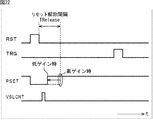
- the timing at which the pixel reset pulse RST is turned off is shifted backward in time to narrow the reset release interval TRelease, so that the reset noise does not reach the stability intentionally for the comparator 44. Release the reset state. As a result, irregular noise can be injected into the reset level AD conversion result.
- the reset noise component appearing on the vertical signal line 21 appears.
- the offset component of the pixel signal (So) is completely removed by turning off the comparator reset pulse PSET for the comparator 44.
- the timing for turning off the pixel reset pulse RST is intentionally shifted backward to reset Reduce the release interval (TRelease).
- the reset state of the comparator 44 is canceled at a timing when the reset noise is not stable. This means that the pulse width of the pixel reset pulse RST for pixel reset is controlled, the settling amount of reset noise of the pixel is controlled, and two-dimensionally irregular noise is injected.
- AD conversion is performed by mixing two-dimensionally irregular fixed pattern noise with the same amount to the reset level or signal level of the pixel signal, and differentially processing each AD conversion result.
- the digital signal of the component is acquired in a state in which quantization noise generated by the differential processing is two-dimensionally spatially random.
- the CMOS image sensor 1 operates at the drive timing shown in FIG. 6 to disperse the distribution of reset levels, thereby avoiding concentration of energy and causing quantization errors caused by differential processing to It prevents the phenomenon that accumulates each time and suppresses the unnatural noise of vertical streaks.
- FIG. 7 is a diagram schematically showing the distribution of the reset level when the shift of the average value of the reset level occurs.
- the horizontal axis indicates the output value of the reset level
- the vertical axis indicates the frequency.
- the drive at the drive timing indicated by the dotted line in FIG. 6 is referred to as “normal drive”, and the drive at the drive timing indicated by the solid line in FIG. 6 is referred to as “dither drive”. .
- the distribution of the reset level is concentrated at the periphery of the average value without spreading the tail. Also, since the noise injection is not performed, the output value of the reset level does not become a large value. Therefore, the output value of the reset level never exceeds the reset level count maximum value.
- the counter 45 does not perform accurate counting, and AD conversion is properly performed. It may be a factor that will not happen. In order to avoid this phenomenon, it is necessary to suppress the shift of the average value of the reset level, but the inventor of the present technology has found a technique for suppressing the shift of the average value of the reset level. Therefore, hereinafter, a CMOS image sensor to which the present technology is applied will be described.
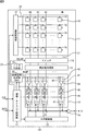
- FIG. 8 is a diagram illustrating a configuration example of a CMOS image sensor as a solid-state imaging device to which the present technology is applied.
- CMOS image sensor 101 of FIG. 8 parts corresponding to those of the CMOS image sensor 1 of FIG. 1 are denoted by the same reference numerals, and the description thereof will be appropriately omitted.
- the CMOS image sensor 101 is different from the CMOS image sensor 1 in that the switch 110 is provided between the pixel array unit 11 and the read current source unit 13.
- the switch 110 is connected to each vertical signal line 21.
- the switch 110 shorts the vertical signal lines 21 in response to the control pulse VSLCNT input from the communication / timing control unit 17 through the control line 23. Then, when the vertical signal lines 21 are short-circuited, the potentials of the vertical signal lines 21 become the average potentials, and by storing them, the shift of the average value of the reset level can be suppressed.
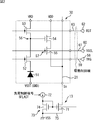
- FIG. 9 illustrates unit pixels 30-1 and unit pixels 30-2 adjacent in the row direction among the unit pixels 30 arranged in a matrix in the pixel array unit 11 for convenience of description.
- parts corresponding to FIG. 2 are given the same reference numerals, and descriptions thereof will be omitted.
- the amplification transistor 54-1 is connected to the vertical signal line 21-1 through the vertical selection transistor 55-1 and constitutes a source follower together with the read current source unit 13-1. .
- the output of the source follower is described as “VSL1”.
- a column AD conversion unit 41-1 is connected to the vertical signal line 21-1.
- the pixel signal from the unit pixel 30-1 is input to one input terminal of the comparator 44-1 via the capacitive element 42-1, and the other input terminal is input.
- the reference signal RAMP from the reference signal generation unit 15 is input through the capacitive element 43-1.
- the output of the capacitive element 42-1 is described as "VSL1D".
- the amplification transistor 54-2 and the read current source unit 13-2 constitute a source follower.
- a column AD conversion unit 41-2 is connected to the vertical signal line 21-2. Further, in FIG. 9 and the like, the output of the source follower is described as “VSL2”, and the output of the capacitive element 42-2 is described as “VSL2D”.
- the switch 110 is composed of a switch transistor 111.
- the source is connected to the vertical signal line 21-1 through the row signal line 112, and the drain is connected to the vertical signal line 21-2 through the row signal line 112. That is, by connecting the vertical signal lines 21 in the row direction with the row signal line 112, the switching transistor 111 is configured to connect the outputs of the source followers configured for each column.
- the control pulse VSLCNT from the communication / timing control unit 17 is input to the gate of the switch transistor 111.
- the switching transistor 111 performs the on / off switching operation in response to the control pulse VSLCNT from the communication / timing control unit 17.
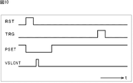
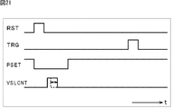
- the control pulse VSLCNT becomes H level only for a certain period of the period in which the comparator reset pulse PSET to the comparator 44 becomes active.
- the switching transistor 111 is turned on to short the vertical signal lines 21 connected to the row signal line 112.
- the potentials of the vertical signal lines 21 become an average potential, and the output of the source follower of each column becomes an averaged output.
- the outputs VSL1 and VSL2 of the source follower are averaged.
- the average value of the output of the source follower is stored as an input capacitance at one input terminal of the comparator 44 arranged in each column AD conversion unit 41.
- the switching transistor 111 is turned off when the control pulse VSLCNT input to the gate becomes L level, and the source before shorting each vertical signal line 21 connected to the row signal line 112 is performed.
- the output of each source follower for each column returns from the average value to an output value according to the variation of the threshold voltage (Vth) of each amplification transistor 54.
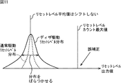
- FIG. 11 is a diagram schematically showing the distribution of the reset level when the shift of the average value of the reset level does not occur.
- the distribution of the reset level is dispersed, but because the average value of the output of the source follower is dispersed, the reset is compared with the case of the normal drive. The average level has not shifted. Therefore, the output value of the reset level does not exceed the reset level count maximum value, and the counter 45 can perform accurate counting. As a result, the AD conversion is properly performed, and the distribution is dispersed, so that the concentration of energy is alleviated, and more surely, the deterioration of the linearity due to the power supply fluctuation and the quantization vertical line caused by the quantization error are suppressed. can do.
- the distribution of the reset level can be broadened by utilizing the characteristics of the capacitive element 42 for signal coupling.
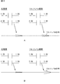
- 12 and 13 show specific examples of DC cutting by the capacitive elements 42-1 and 42-2 (FIG. 9) in the auto-zero period (AZ period) and the reset level period and the distribution of the reset level at that time. .
- FIG. 12A for comparison with FIG. 12B, distribution of DC cut voltage values in the case of normal driving and the reset level at that time is shown.
- the input voltages of capacitive elements 42-1 and 42-2 in the auto-zero period are 1.0 V and 2.0 V, respectively, and the output voltage is 1.8. Aligned to V.
- the input voltages of the capacitive elements 42-1 and 42-2 in the reset level period are 1.0 V and 2.0 V, respectively, and the output voltages are cut to 1.8 V by DC cutting. Further, in normal driving, the distribution of reset levels in the reset level period hardly varies as in the auto-zero period, and the tail does not spread.
- FIG. 12B shows the distribution of the voltage value of DC cut and the reset level at that time when the driving at the driving timing shown in FIG. 10 is performed.
- the switching transistor 111 since the switching transistor 111 is turned on and the outputs of the source followers in the respective columns are averaged, the input voltages of the capacitive elements 42-1 and 42-2 in the auto-zero period are equalized to 1.5V. Then, the DC-cut by the capacitive elements 42-1 and 42-2 results in an output voltage of 1.8 V.
- the switching transistor 111 is turned off, and the vertical signal lines 21-1 and 21-2 are returned to the original state. Therefore, the input voltages of the capacitive elements 42-1 and 42-2 in the reset level period are 1.0. It becomes V, 2.0V. Then, when DC-cut by the capacitive elements 42-1 and 42-2, the output voltage becomes 1.3 V and 2.3 V, respectively, depending on the characteristics of the capacitive elements 42.
- the input voltage is adjusted to 1.5 V which is the average value of the output of the source follower in the auto zero period, and 1.0 V and 2.0 V are input as the input voltage in the subsequent reset level period. Then, since the output voltage varies to 1.3 V and 2.3 V, the distribution of the reset level in the reset level period is a broadened one.
- the width of the distribution of reset levels can be expanded compared to the normal drive of FIG. 12A.
- FIG. 13 A of FIG. 13 is shown for comparison with B of FIG. 13, and is the same as A of FIG. 13.
- B of FIG. 13 shows the distribution of the voltage value of DC cut and the reset level at that time in the case of driving at the driving timing shown in FIG.
- the switching transistor 111 is turned on, but is turned off before the outputs of the source followers in each column are completely averaged, so the capacitive element 42-1 in the auto-zero period is , 42-2 are 1.2 V and 1.8 V respectively without being equal. Then, the DC-cut by the capacitive elements 42-1 and 42-2 results in an output voltage of 1.8 V.
- the input voltages of the capacitive elements 42-1 and 42-2 are 1.0 V and 2.0 V, respectively. Then, when DC-cut by the capacitive elements 42-1 and 42-2, the output voltage becomes 1.6 V and 2.0 V, respectively, depending on the characteristics of the capacitive elements 42.
- the input voltage is brought close to the average value (for example, 1.5 V) of the output of the source follower as in 1.2 V and 1.8 V respectively in the auto-zero period, and the input voltage in the subsequent reset level period.
- the output voltage fluctuates to 1.6 V and 2.0 V, so the distribution of the reset level in the reset level period has a broadened tail.
- the distribution of reset levels in the reset level period of B in FIG. 13 is not the one in which the input voltage is completely averaged, the distribution of the reset levels is smaller than the distribution of reset levels in the reset level period of B in FIG. Although the width is narrowed, noise can be injected as much as the distribution spreads.
- the width of the distribution of reset levels can be expanded compared to the normal drive of A of FIG.
- FIG. 14 is a diagram showing a drive circuit used for normal drive.
- the outputs VSL1 and VSL2 are constant at 2.0 V and 1.0 V, respectively.
- outputs VSL1D and VSL2D of the capacitive element 42 are DC-cut by the capacitive element 42 as described in A of FIG. 12 and A of FIG. Be aligned.
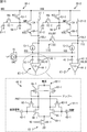
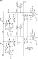
- FIG. 16 is a diagram showing a drive circuit used to drive the present technology.
- the row signal line 112 is connected to the vertical signal lines 21-1 and 21-2 in order to average the output of the source follower of each column, and the switching transistor 111 is provided. Therefore, the drive of the present technology is driven as shown in the timing chart of FIG. 17 or FIG.
- the voltage values of the outputs VSL1 and VSL2 of the source follower decrease in the auto-zero period.
- the control pulse VSLCNT when the control pulse VSLCNT is turned on, the vertical signal lines 21 are short-circuited by the switch transistor 111, and the output of the source follower of each column is averaged.
- the outputs VSL1 and VSL2 have an average value of 1.5V. That is, by short-circuiting the vertical signal lines 21 with each other by the horizontal connection, the outputs of the respective source followers are averaged.
- the outputs VSL1D and VSL2D of the capacitive element 42 are DC-cut by the capacitive element 42 as described in B of FIG. 12, the outputs VSL1D and VSL2D are 1.8 V after DC-cut at time t24. Aligned with
- the control pulse VSLCNT is turned off to return to the original state before the vertical signal lines 21 are shorted. Therefore, the voltage values of the outputs VSL1 and VSL2 of the source follower are 2.0 in the reset level period. It becomes V, 1.0V. Then, in the on period of the drive pulse TRG from time t25 to time t26, and in the signal level period after time t26, the outputs VSL1 and VSL2 have constant voltage values of 2.0 V and 1.0 V, respectively.
- the outputs VSL1D and VSL2D of the capacitive element 42 are DC-cut by the capacitive element 42 as described in B of FIG. 12, the outputs VSL1D and VSL2D are 2.3 V and 1.3 V, respectively, depending on their characteristics. It becomes. That is, when the control pulse VSLCNT is turned off, the output of each source follower moves, and the node after DC cut follows the output of each source follower, and the distribution of the reset level is dispersed. As a result, noise is added to the pixel signal transmitted through the vertical signal line 21.
- control pulse VSLCNT is turned on, but control is performed at time t34 earlier in time than the time when the output of the source follower of each column is completely averaged. Since the pulse VSLCNT is turned off, the outputs VSL1 and VSL2 become 1.8 V and 1.2 V, respectively.
- the control pulse VSLCNT is turned off to return to the original state before the vertical signal lines 21 are shorted. Therefore, the voltage values of the outputs VSL1 and VSL2 of the source follower are 2.0 in the reset level period. It becomes V, 1.0V. Then, in the on period of the drive pulse TRG from time t35 to time t36, and in the signal level period after time t36, the outputs VSL1 and VSL2 have constant voltage values of 2.0 V and 1.0 V, respectively.
- the outputs VSL1D and VSL2D of the capacitive element 42 are DC-cut by the capacitive element 42 as described in B of FIG. 13, the outputs VSL1D and VSL2D are 1.8 V after DC-cut at time t34. Aligned with Thereafter, after time t34, the outputs VSL1D and VSL2D become 2.0 V and 1.6 V according to the characteristics of the capacitive element 42.
- the node after DC cutting follows the output of each source follower and is not as good as when the output of the source follower is completely averaged.
- the distribution of reset levels will vary. In other words, the width of the distribution of the reset level can be adjusted according to the pulse width of the control pulse VSLCNT.
- the width of the distribution of reset levels can be expanded compared to the normal drive in FIG. 15.
- the drive of the present technology in the case of injecting noise for the purpose of suppressing concentration of energy, quantization vertical lines, etc., no shift of the average value of the reset level is generated, and the distribution of reset levels is dispersed. It can be turned. As a result, since the AD conversion is properly performed, it is possible to more reliably suppress the deterioration of the linearity in the AD conversion and the quantization vertical line caused by the quantization error.
- quantization errors are accumulated in each result of performing differential processing between the AD conversion result of the reset level and the AD conversion result of the signal level.
- vertical streak noise due to quantization error will be visible.
- the shift of the average value of the reset level can be suppressed only by providing the switching transistor 111, so that the circuit scale does not increase.
- noise is added to the pixel signal transmitted through the vertical signal line 21 by shorting the vertical signal line 21.
- the addition unit 19 may add noise that is invariant in time and irregular in two-dimensional space.
- the unit pixels 30 arranged in the pixel array unit 11 correspond to color imaging. That is, in the plurality of unit pixels 30 two-dimensionally arranged in a matrix in the pixel array unit 11, the light receiving surface on which the light of each photodiode 51 is incident is a color filter of a plurality of colors for capturing a color image. A color filter of any of the color separation filters consisting of a combination is provided.
- the example shown in FIG. 20 uses a color filter of the so-called Bayer Arrangement basic form, and unit pixels 30 two-dimensionally arranged in a matrix are red (R), green (G), blue ( In order to correspond to the three-color color filter of B), the repeating unit of the color separation filter is arranged in 2 ⁇ 2 pixels to constitute the pixel array unit 11.
- a first color pixel for sensing a first color (e.g. R) is arranged in the odd row odd column, and a second color (e.g. G) is arranged in the odd row even column and the even row odd column.
- a second color pixel for sensing is disposed, and a third color pixel for sensing a third color (eg, B) is disposed in the even-numbered row and the even-numbered column.
- two color pixels of R / G or G / B different for each row are arranged in a checkered pattern.
- the color arrangement of color filters in the basic form of such Bayer arrangement is repeated every two colors of R / G or G / B in both row direction and column direction, but every color of color pixel
- a switching transistor 111 can be provided to connect each vertical signal line 21 by a row signal line 112 for each color, so that outputs of source followers of the same color can be combined.
- the vertical signal lines 21 in odd columns to which color pixels in odd columns (R or G) are connected are connected in the row direction by the row signal line 112-1, and the outputs of their source followers To be connected.
- vertical signal lines 21 of even columns to which color pixels of even columns (G or B) are connected are connected in a row direction by row signal line 112-2 and the outputs of their source followers are connected to each other.
- the switch transistor 111-1 to which the control pulse VSLCNT is input to the gate is provided on the row signal line 112-1 in which the vertical signal lines 21 in the odd columns are connected for each color. Further, on the row signal line 112-2 in which the vertical signal lines 21 in the even-numbered columns are connected for each color, the switch transistor 111-1 to which the control pulse VSLCNT is input to its gate is provided.
- the switching transistors 111-1 and 112-2 perform switching operation according to the control pulse VSLCNT, thereby shorting out the vertical signal lines 21 of the odd-numbered column or the even-numbered column, and thereby the source follower for each color.
- the output of can be averaged.
- the gain of AD conversion is adjusted by changing the slope of the slope of the reference signal RAMP generated by the reference signal generation unit 15. Specifically, as the inclination of the reference signal RAMP is gentler, the point at which the reference signal RAMP matches the pixel signal transmitted through the vertical signal line 21 is later, so that a large digital signal can be obtained. Gain of AD conversion increases. Conversely, when the slope of the reference signal RAMP is steep, the gain of AD conversion is low.
- the slope when capturing the reset level is also halved, so the slope is halved. If it is the same distribution as before, it will be out of the range of the reference signal RAMP, and it will not be possible to capture the reset level.
- the control pulse VSLCNT is set to H level only for a fixed period during a period (auto zero period) in which the comparator reset pulse PSET to the comparator 44 is active. Adjust the level period according to the AD conversion gain. Specifically, when the gain of AD conversion is increased, the pulse width of the control pulse VSLCNT is narrowed so that the distribution of the reset level does not spread. On the other hand, when the gain of AD conversion is lowered, the pulse width of the control pulse VSLCNT is broadened so that the distribution of reset levels is broadened.
- the pulse width of the comparator reset pulse PSET can also be adjusted in conjunction with the above-described AD conversion gain.
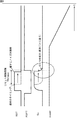
- the pulse width of the comparator reset pulse PSET is narrowed as shown by the solid line in FIG.
- the rising edge of the reset pulse RST is approached.
- the reset release interval TRelease is narrowed, and the comparator 44 is turned off by the comparator reset pulse PSET before the reset noise appearing on the vertical signal line 21 is stabilized, thereby positively injecting the reset noise.
- the slope of the reference signal RAMP is steep and the AD conversion gain is high, the stability of the AD conversion is prioritized, and the pulse width of the comparator reset pulse PSET is widened as shown by the dotted line in FIG.
- the reset release interval TRelease is made as wide as normal timing, and after the reset noise is stabilized, the comparator 44 is turned off by the comparator reset pulse PSET.
- DACs 15a corresponding to odd columns and DACs 15b corresponding to even columns are provided.
- the DACs 15 a and 15 b generate stepped sawtooth waves (ramp waveforms) based on the control signal from the communication / timing control unit 17.
- the DACs 15a and 15b supply the generated stepped sawtooth waves to the column AD conversion units 41 of the column processing unit 14 as reference signals RAMPa and RAMPb.
- the reference signal generation unit 15 when the control signal for generating the reference signals RAMPa and RAMPb is supplied from the communication / timing control unit 17, one of the colors existing on the row control line 20 (R in odd column or The DAC 15a generates a reference signal RAMPa having a slope .beta.a matched to the color pixel characteristics of G) and having a step-like waveform which is temporally changed in a sawtooth shape as a whole. Then, the DAC 15 a supplies the generated reference signal RAMPa to the other input terminal of the comparator 44 of the column AD conversion unit 41 corresponding to the odd-numbered column via the capacitive element 43.
- the reference signal RAMPb is generated by the DAC 15 b. Then, the DAC 15 b supplies the generated reference signal RAMPb to the other input terminal of the comparator 44 of the column AD conversion unit 41 corresponding to the even number column via the capacitive element 43.
- the DAC for generating the reference signal RAMP is not prepared for all the color filters in the color separation filter but in the repetition cycle of colors determined by the type and arrangement of colors. It is made to provide only the part according to the combination of the predetermined color according to.
- the combination of predetermined colors present in the row to be processed is switched, and accordingly, the change characteristics (for example, the slope ⁇ a) of the reference signals RAMPa and RAMPb generated by the DACs 15a and 15b. , ⁇ b) and the initial value are switched according to the color filter, that is, the characteristics of the pixel signal.
- the control pulse VSLCNTa is input to the gate of the switch transistor 111-1 and the switch
- the control pulse VSLCNTb is input to the gate of the transistor 111-2.
- the switching transistors 111-1 and 111-2 can be separately controlled to, for example, average the output of the source follower or adjust the width of the distribution of the reset level.
- connection form of switch transistor Although the connection form of the switch transistor 111 is described, connection forms other than the connection form shown in FIG. 9 may be employed.
- FIG. 24 shows another connection of the switch transistor 111.
- the gate is connected to the communication / timing control unit 17 through the control line 23, the source is connected to the vertical signal line 21-1, and the drain is It is connected to the row signal line 112.
- the gate is connected to the control line 23, the source is connected to the vertical signal line 21-2, and the drain is connected to the row signal line 112.
- the switching transistors 111-1 and 111-2 perform the switching operation according to the control pulse VSLCNT input to the gates, thereby the vertical signal lines 21-1 and 21-. 2 can be shorted.
- connection form of FIG. 24 is an example of another connection form of the switch transistor 111, and still another connection form can be adopted.
- the point is that the switching transistor 111 only needs to short the vertical signal lines 21 by the switching operation, and the connection form between the vertical signal lines 21 and the row signal lines 112 is arbitrary.
- the switching transistor 111 may be connected to all the vertical signal lines 21 (H0, H1,..., Hh), or all the vertical signal lines 21 (H0, H1,. , Hh) may be connected to some of the vertical signal lines 21 (for example, H 0, H 2, H 4,... In odd columns). Further, when connected to a part of the vertical signal line 21, for example, by dividing the vertical signal line 21 into blocks in predetermined units, each block is connected to the switch transistor 111. be able to.
- a plurality of unit pixels 30 arranged in a matrix adopts a pixel sharing configuration in which at least the amplifying transistor 54 and the vertical signal line 21 are shared with other unit pixels other than itself. You may
- solid of a solid-state imaging device means that it is made of a semiconductor.
- the present technology is not limited to application to a solid-state imaging device. That is, the present technology includes an imaging device such as a digital still camera or a video camera, a portable terminal device having an imaging function, a copying machine using a solid-state imaging device as an image reading unit, and a solid image capturing unit (photoelectric conversion unit).
- the present invention can be applied to general electronic devices using an imaging device.
- the solid-state imaging device may be formed as a single chip, or may be a modular form having an imaging function in which an imaging unit and a signal processing unit or an optical system are packaged together.
- FIG. 25 is a block diagram illustrating a configuration example of an imaging device as an electronic device to which the present technology is applied.
- the imaging apparatus 300 in FIG. 25 includes an optical unit 301 including a lens group, a solid-state imaging device (imaging device) 302 in which each configuration of the unit pixel 30 described above is adopted, and a DSP (Digital Signal) that is a camera signal processing circuit. Processor) circuit 303 is provided.
- the imaging apparatus 300 also includes a frame memory 304, a display unit 305, a recording unit 306, an operation unit 307, and a power supply unit 308.
- the DSP circuit 303, the frame memory 304, the display unit 305, the recording unit 306, the operation unit 307, and the power supply unit 308 are mutually connected via a bus line 309.
- the optical unit 301 captures incident light (image light) from a subject and forms an image on the imaging surface of the solid-state imaging device 302.
- the solid-state imaging device 302 converts the light amount of incident light focused on the imaging surface by the optical unit 301 into an electrical signal in pixel units and outputs the electrical signal as a pixel signal.
- a solid-state imaging device such as the CMOS image sensor 1 according to the above-described embodiment, that is, a solid-state imaging device capable of realizing imaging without distortion by global exposure can be used.
- the display unit 305 includes, for example, a panel type display device such as a liquid crystal panel or an organic EL (Electro Luminescence) panel, and displays a moving image or a still image captured by the solid-state imaging device 302.
- the recording unit 306 records a moving image or a still image captured by the solid-state imaging device 302 on a recording medium.
- the operation unit 307 issues operation commands for various functions of the imaging device 300 under the operation of the user.
- the power supply unit 308 appropriately supplies various power supplies serving as operation power supplies of the DSP circuit 303, the frame memory 304, the display unit 305, the recording unit 306, and the operation unit 307 to these supply targets.
- the present invention has been described by way of example in which the present invention is applied to a CMOS image sensor in which unit pixels 30 for detecting signal charges according to the amount of visible light as physical quantities are arranged in a matrix.
- the present technology is not limited to the application to a CMOS image sensor, and is applicable to all solid-state imaging devices of a column system in which a column processing unit is disposed for each pixel row of the pixel array unit.
- the present technology is not limited to application to a solid-state imaging device that detects the distribution of incident light quantity of visible light and captures an image as an image, and a solid that captures distribution of incident quantity of infrared light, X-rays, or particles as an image
- a solid-state imaging device that detects the distribution of incident light quantity of visible light and captures an image as an image
- a solid that captures distribution of incident quantity of infrared light, X-rays, or particles as an image
- solid-state imaging devices physical quantity distribution detection devices
- an imaging device and a fingerprint detection sensor that senses the distribution of other physical quantities such as pressure and capacitance in a broad sense and captures an image as an image is there.
- the present technology can have the following configurations.
- a pixel portion in which a plurality of pixels for performing photoelectric conversion are arranged in a matrix A column signal line for transmitting a pixel signal output from the pixel for each column; It has a comparator for comparing a reference signal which is a ramp wave with the pixel signal transmitted through the column signal line, and based on the comparison result of the comparator, the reference level and the signal level of the pixel signal are made independent.
- AD converter to convert digital signals into A switch connected to the column signal line, A control unit configured to turn on the switch only for a predetermined period during a period in which the comparator is reset to short the column signal lines;
- the plurality of pixels are arranged corresponding to a color filter in which colors are arranged in a predetermined repeating unit,
- the solid-state imaging device according to (1), wherein the switch is connected to each of the column signal lines of pixels of the same color.
- the control unit adjusts the on period of the switch according to a gain of AD conversion performed by the AD conversion unit.
- the solid-state imaging device according to any one of (1) to (3), wherein the control unit adjusts a reset period of the comparator according to a gain of AD conversion performed by the AD conversion unit.
- the solid-state imaging device according to any one of (1) to (4), wherein a gain of AD conversion performed by the AD conversion unit has a value corresponding to the reference signal which is different for each color.
- the switch is a transistor, The transistor has a gate connected to the control unit through a control line, and a source and a drain connected to a row signal line connected to the column signal line in the row direction (1) to (5)
- the solid-state imaging device according to any one of the preceding items.
- the switch is a transistor, The transistor has a gate connected to the control unit through a control line, a source connected to the column signal line, and a drain connected to a row signal line in the row direction (1) to (5)
- the solid-state image sensor as described in any one.
- the column signal lines are divided into blocks in predetermined units, The solid-state imaging device according to any one of (1) to (7), wherein the switch is connected to the column signal line for each block.
- the plurality of pixels arranged in a matrix in the pixel portion share at least a transistor for amplification and the column signal line with another pixel according to any one of (1) to (9).
- Solid-state image sensor (11)
- the pixel signal transmitted through the column signal line further includes a noise addition unit that adds temporally invariant and two-dimensional spatially irregular noise to any one of (1) to (10).
- the solid-state image sensor as described in a term.
- (12) A pixel portion in which a plurality of pixels for performing photoelectric conversion are arranged in a matrix; A column signal line for transmitting a pixel signal output from the pixel for each column; It has a comparator for comparing a reference signal which is a ramp wave with the pixel signal transmitted through the column signal line, and based on the comparison result of the comparator, the reference level and the signal level of the pixel signal are made independent.
- AD converter to convert digital signals into And a switch connected to the column signal line.
- the solid-state imaging device is Driving the switches only for a predetermined period of time during which the comparators are reset, and shorting the column signal lines together.
- (13) A pixel portion in which a plurality of pixels for performing photoelectric conversion are arranged in a matrix; A column signal line for transmitting a pixel signal output from the pixel for each column; It has a comparator for comparing a reference signal which is a ramp wave with the pixel signal transmitted through the column signal line, and based on the comparison result of the comparator, the reference level and the signal level of the pixel signal are made independent.
- AD converter to convert digital signals into A switch connected to the column signal line, A control unit which turns on the switch only for a predetermined period of time during a period in which the comparator is reset, and shorts the column signal lines; and an electronic device equipped with a solid-state imaging device.
- CMOS image sensor 11 pixel array unit, 13 readout current source unit, 14 column processing unit, 15 reference signal generation unit, 15a, 15b DAC, 17 communication and timing control unit, 19 noise addition unit, 20 row control line , 21 vertical signal line, 23 control line, 30 unit pixel, 41 column AD conversion unit, 42 capacitive element, 43 capacitive element, 44 comparator, 45 counter, 54 transistor for amplification, 110 switch, 111 switch transistor, 112 line Signal line, 300 imaging device, 302 solid-state imaging device
Landscapes
- Engineering & Computer Science (AREA)
- Multimedia (AREA)
- Signal Processing (AREA)
- Transforming Light Signals Into Electric Signals (AREA)
- Solid State Image Pick-Up Elements (AREA)
Abstract
Description
図1は、従来のCMOSイメージセンサの構成を示す図である。
ここで、図1のカラム処理部14と参照信号生成部15の詳細な構成について説明する。
次に、図2を参照して、図1のCMOSイメージセンサ1の画素アレイ部11に配置される単位画素30の構成例と、駆動制御線と画素トランジスタの接続形態について説明する。
次に、図3を参照して、図1の各カラムAD変換部41に設けられる比較器44の詳細について説明する。
ところで、CMOSイメージセンサ1においては、AD変換に際して、ノイズ付加部19等が所定のノイズを注入してリセットレベルの分布をばらつかせることで、カラムAD変換部41の動作時間をずらしてエネルギーの集中を避けたり、量子化誤差起因の縦筋を抑制したりしているが、リセットレベルの分布がばらつくと同時に、リセットレベルの平均値がシフトするという現象が発生してしまうことが分かった。
図8は、本技術が適用される固体撮像素子としてのCMOSイメージセンサの構成例を示す図である。
図14は、通常の駆動に用いられる駆動回路を示す図である。
図16は、本技術の駆動に用いられる駆動回路を示す図である。
ところで、図8のCMOSイメージセンサ101において、画素アレイ部11に配置される単位画素30はカラー撮像に対応している。すなわち、画素アレイ部11に行列状に2次元配置された複数の単位画素30において、各フォトダイオード51の光が入射される受光面には、カラー画像を撮像するための複数色の色フィルタの組み合わせからなる色分解フィルタのいずれかの色フィルタが設けられている。
図8のCMOSイメージセンサ101においては、参照信号生成部15により生成される参照信号RAMPのスロープの傾きを変化させることで、AD変換のゲインを調整している。具体的には、参照信号RAMPの傾きが緩やかなほど、参照信号RAMPと、垂直信号線21を通じて伝送される画素信号とが一致する時点が遅くなるので、大きなデジタル信号が得られるようになり、AD変換のゲインが高くなる。逆に、参照信号RAMPの傾きが急な場合にはAD変換のゲインが低くなる。
また、前述したAD変換のゲインと連動させて、比較器リセットパルスPSETのパルス幅を調整することもできる。
図20に示したように、図8のCMOSイメージセンサ101では、例えば、ベイヤ配列の基本形のカラーフィルタが用いられ、それに対応して単位画素30が配置されている。また、先に述べたように、色フィルタの繰り返しは、2行及び2列ごととなる。ここでは、行単位で画素信号を読み出して、垂直信号線21ごとに列ごとに設けられたカラムAD変換部41に画素信号を入力するので、1つの処理対象行には、R/G又はG/Bのいずれか2色のみの画素信号が存在することになる。
スイッチ用トランジスタ111の接続形態であるが、図9に示した接続形態以外の接続形態を採用することもできる。図24には、スイッチ用トランジスタ111の他の接続形態を示している。
光電変換を行う複数の画素が行列状に配置された画素部と、
前記画素から出力される画素信号を列ごとに伝送する列信号線と、
ランプ波である参照信号と、前記列信号線を通して伝送される前記画素信号とを比較する比較器を有し、前記比較器の比較結果に基づいて、前記画素信号の基準レベルと信号レベルを独立にデジタル信号に変換するAD変換部と、
前記列信号線と接続されるスイッチと、
前記比較器をリセットする期間のうち、一定期間のみ前記スイッチをオンさせて、前記列信号線同士をショートさせる制御部と
を備える固体撮像素子。
(2)
前記画素部には、所定の繰り返し単位で色が配列されたカラーフィルタに対応して前記複数の画素が配置されており、
前記スイッチは、同色の画素の前記列信号線ごとに接続される
(1)に記載の固体撮像素子。
(3)
前記制御部は、前記AD変換部によるAD変換のゲインに応じて、前記スイッチのオン期間を調整する
(1)又は(2)に記載の固体撮像素子。
(4)
前記制御部は、前記AD変換部によるAD変換のゲインに応じて、前記比較器のリセット期間を調整する
(1)乃至(3)のいずれか一項に記載の固体撮像素子。
(5)
前記AD変換部によるAD変換のゲインは、色ごとに異なる前記参照信号に応じた値となる
(1)乃至(4)のいずれか一項に記載の固体撮像素子。
(6)
前記スイッチは、トランジスタであり、
前記トランジスタは、制御線を通して前記制御部に接続されるゲートと、前記列信号線と行方向に接続された行信号線に接続されるソース及びドレインとを有する
(1)乃至(5)のいずれか一項に記載の固体撮像素子。
(7)
前記スイッチは、トランジスタであり、
前記トランジスタは、制御線を通して前記制御部に接続されるゲートと、前記列信号線に接続されるソースと、行方向の行信号線に接続されるドレインとを有する
(1)乃至(5)のいずれか一項に記載の固体撮像素子。
(8)
前記スイッチは、全ての前記列信号線と接続されている
(1)乃至(7)のいずれか一項に記載の固体撮像素子。
(9)
前記列信号線は、所定の単位でブロックに分けられており、
前記スイッチは、前記ブロックごとに前記列信号線と接続されている
(1)乃至(7)のいずれか一項に記載の固体撮像素子。
(10)
前記画素部に行列状に配置された複数の画素は、他の画素と、増幅用のトランジスタ及び前記列信号線を少なくとも共有している
(1)乃至(9)のいずれか一項に記載の固体撮像素子。
(11)
前記列信号線を通して伝送される前記画素信号に、時間的には不変でかつ2次元空間的には不規則なノイズを付加するノイズ付加部をさらに備える
(1)乃至(10)のいずれか一項に記載の固体撮像素子。
(12)
光電変換を行う複数の画素が行列状に配置された画素部と、
前記画素から出力される画素信号を列ごとに伝送する列信号線と、
ランプ波である参照信号と、前記列信号線を通して伝送される前記画素信号とを比較する比較器を有し、前記比較器の比較結果に基づいて、前記画素信号の基準レベルと信号レベルを独立にデジタル信号に変換するAD変換部と、
前記列信号線と接続されるスイッチと
を備える固体撮像素子の駆動方法において、
前記固体撮像素子が、
前記比較器をリセットする期間のうち、一定期間のみ前記スイッチをオンさせて、前記列信号線同士をショートさせるステップ
を含む駆動方法。
(13)
光電変換を行う複数の画素が行列状に配置された画素部と、
前記画素から出力される画素信号を列ごとに伝送する列信号線と、
ランプ波である参照信号と、前記列信号線を通して伝送される前記画素信号とを比較する比較器を有し、前記比較器の比較結果に基づいて、前記画素信号の基準レベルと信号レベルを独立にデジタル信号に変換するAD変換部と、
前記列信号線と接続されるスイッチと、
前記比較器をリセットする期間のうち、一定期間のみ前記スイッチをオンさせて、前記列信号線同士をショートさせる制御部と
を備える
固体撮像素子を搭載した電子機器。
Claims (13)
- 光電変換を行う複数の画素が行列状に配置された画素部と、
前記画素から出力される画素信号を列ごとに伝送する列信号線と、
ランプ波である参照信号と、前記列信号線を通して伝送される前記画素信号とを比較する比較器を有し、前記比較器の比較結果に基づいて、前記画素信号の基準レベルと信号レベルを独立にデジタル信号に変換するAD変換部と、
前記列信号線と接続されるスイッチと、
前記比較器をリセットする期間のうち、一定期間のみ前記スイッチをオンさせて、前記列信号線同士をショートさせる制御部と
を備える固体撮像素子。 - 前記画素部には、所定の繰り返し単位で色が配列されたカラーフィルタに対応して前記複数の画素が配置されており、
前記スイッチは、同色の画素の前記列信号線ごとに接続される
請求項1に記載の固体撮像素子。 - 前記制御部は、前記AD変換部によるAD変換のゲインに応じて、前記スイッチのオン期間を調整する
請求項2に記載の固体撮像素子。 - 前記制御部は、前記AD変換部によるAD変換のゲインに応じて、前記比較器のリセット期間を調整する
請求項3に記載の固体撮像素子。 - 前記AD変換部によるAD変換のゲインは、色ごとに異なる前記参照信号に応じた値となる
請求項4に記載の固体撮像素子。 - 前記スイッチは、トランジスタであり、
前記トランジスタは、制御線を通して前記制御部に接続されるゲートと、前記列信号線と行方向に接続された行信号線に接続されるソース及びドレインとを有する
請求項1に記載の固体撮像素子。 - 前記スイッチは、トランジスタであり、
前記トランジスタは、制御線を通して前記制御部に接続されるゲートと、前記列信号線に接続されるソースと、行方向の行信号線に接続されるドレインとを有する
請求項1に記載の固体撮像素子。 - 前記スイッチは、全ての前記列信号線と接続されている
請求項1に記載の固体撮像素子。 - 前記列信号線は、所定の単位でブロックに分けられており、
前記スイッチは、前記ブロックごとに前記列信号線と接続されている
請求項1に記載の固体撮像素子。 - 前記画素部に行列状に配置された複数の画素は、他の画素と、増幅用のトランジスタ及び前記列信号線を少なくとも共有している
請求項1に記載の固体撮像素子。 - 前記列信号線を通して伝送される前記画素信号に、時間的には不変でかつ2次元空間的には不規則なノイズを付加するノイズ付加部をさらに備える
請求項1に記載の固体撮像素子。 - 光電変換を行う複数の画素が行列状に配置された画素部と、
前記画素から出力される画素信号を列ごとに伝送する列信号線と、
ランプ波である参照信号と、前記列信号線を通して伝送される前記画素信号とを比較する比較器を有し、前記比較器の比較結果に基づいて、前記画素信号の基準レベルと信号レベルを独立にデジタル信号に変換するAD変換部と、
前記列信号線と接続されるスイッチと
を備える固体撮像素子の駆動方法において、
前記固体撮像素子が、
前記比較器をリセットする期間のうち、一定期間のみ前記スイッチをオンさせて、前記列信号線同士をショートさせるステップ
を含む駆動方法。 - 光電変換を行う複数の画素が行列状に配置された画素部と、
前記画素から出力される画素信号を列ごとに伝送する列信号線と、
ランプ波である参照信号と、前記列信号線を通して伝送される前記画素信号とを比較する比較器を有し、前記比較器の比較結果に基づいて、前記画素信号の基準レベルと信号レベルを独立にデジタル信号に変換するAD変換部と、
前記列信号線と接続されるスイッチと、
前記比較器をリセットする期間のうち、一定期間のみ前記スイッチをオンさせて、前記列信号線同士をショートさせる制御部と
を備える
固体撮像素子を搭載した電子機器。
Priority Applications (10)
| Application Number | Priority Date | Filing Date | Title |
|---|---|---|---|
| CN201480007095.8A CN104969539B (zh) | 2013-02-27 | 2014-02-17 | 固体摄像器件、固体摄像器件驱动方法和电子设备 |
| US14/768,534 US9544519B2 (en) | 2013-02-27 | 2014-02-17 | Solid-state imaging device, driving method, and electronic device |
| JP2015502865A JP6332263B2 (ja) | 2013-02-27 | 2014-02-17 | 固体撮像素子、駆動方法、及び、電子機器 |
| EP18175261.9A EP3389258B1 (en) | 2013-02-27 | 2014-02-17 | Solid-state imaging device, driving method, and electronic device |
| EP14756681.4A EP2963918B1 (en) | 2013-02-27 | 2014-02-17 | Solid-state imaging device, driving method, and electronic device |
| KR1020157020333A KR101721350B1 (ko) | 2013-02-27 | 2014-02-17 | 고체 촬상 소자, 구동 방법, 및, 전자 기기 |
| US15/352,207 US9661253B2 (en) | 2013-02-27 | 2016-11-15 | Solid-state imaging device, driving method, and electronic device |
| US15/489,223 US9838654B2 (en) | 2013-02-27 | 2017-04-17 | Solid-state imaging device, driving method, and electronic device |
| US15/792,065 US10070103B2 (en) | 2013-02-27 | 2017-10-24 | Solid-state imaging device, driving method, and electronic device |
| US16/041,128 US20180352200A1 (en) | 2013-02-27 | 2018-07-20 | Solid-state imaging device, driving method, and electronic device |
Applications Claiming Priority (2)
| Application Number | Priority Date | Filing Date | Title |
|---|---|---|---|
| JP2013037868 | 2013-02-27 | ||
| JP2013-037868 | 2013-02-27 |
Related Child Applications (2)
| Application Number | Title | Priority Date | Filing Date |
|---|---|---|---|
| US14/768,534 A-371-Of-International US9544519B2 (en) | 2013-02-27 | 2014-02-17 | Solid-state imaging device, driving method, and electronic device |
| US15/352,207 Continuation US9661253B2 (en) | 2013-02-27 | 2016-11-15 | Solid-state imaging device, driving method, and electronic device |
Publications (1)
| Publication Number | Publication Date |
|---|---|
| WO2014132822A1 true WO2014132822A1 (ja) | 2014-09-04 |
Family
ID=51428094
Family Applications (1)
| Application Number | Title | Priority Date | Filing Date |
|---|---|---|---|
| PCT/JP2014/053597 Ceased WO2014132822A1 (ja) | 2013-02-27 | 2014-02-17 | 固体撮像素子、駆動方法、及び、電子機器 |
Country Status (8)
| Country | Link |
|---|---|
| US (5) | US9544519B2 (ja) |
| EP (2) | EP2963918B1 (ja) |
| JP (1) | JP6332263B2 (ja) |
| KR (1) | KR101721350B1 (ja) |
| CN (4) | CN107706202B (ja) |
| DE (1) | DE202014011038U1 (ja) |
| TW (2) | TWI634791B (ja) |
| WO (1) | WO2014132822A1 (ja) |
Cited By (11)
| Publication number | Priority date | Publication date | Assignee | Title |
|---|---|---|---|---|
| JP2015056840A (ja) * | 2013-09-13 | 2015-03-23 | 株式会社東芝 | 固体撮像装置 |
| JP2015177421A (ja) * | 2014-03-17 | 2015-10-05 | オリンパス株式会社 | 撮像装置 |
| JP2018182496A (ja) * | 2017-04-11 | 2018-11-15 | ソニーセミコンダクタソリューションズ株式会社 | 信号処理装置、及び、固体撮像装置 |
| EP3579549A2 (en) | 2018-06-08 | 2019-12-11 | Canon Kabushiki Kaisha | Imaging apparatus, imaging system, moving body, and semiconductor substrate for lamination |
| WO2020045373A1 (ja) * | 2018-08-30 | 2020-03-05 | ソニーセミコンダクタソリューションズ株式会社 | 固体撮像装置 |
| JP2021064859A (ja) * | 2019-10-11 | 2021-04-22 | キヤノン株式会社 | 光電変換装置及び撮像システム |
| WO2021095450A1 (ja) * | 2019-11-13 | 2021-05-20 | ソニーセミコンダクタソリューションズ株式会社 | 撮像素子、光検出素子、及び、電子機器 |
| US11323646B2 (en) | 2018-07-24 | 2022-05-03 | Sony Semiconductor Solutions Corporation | Imaging device |
| JP2023084647A (ja) * | 2021-12-07 | 2023-06-19 | キヤノン株式会社 | 光電変換装置 |
| JP2023111020A (ja) * | 2022-01-31 | 2023-08-10 | キヤノン株式会社 | 撮像素子の制御方法、撮像素子及びプログラム |
| JP2024097946A (ja) * | 2021-12-07 | 2024-07-19 | キヤノン株式会社 | 光電変換装置 |
Families Citing this family (48)
| Publication number | Priority date | Publication date | Assignee | Title |
|---|---|---|---|---|
| JP5935274B2 (ja) | 2011-09-22 | 2016-06-15 | ソニー株式会社 | 固体撮像装置、固体撮像装置の制御方法および固体撮像装置の制御プログラム |
| JP6391290B2 (ja) * | 2014-05-08 | 2018-09-19 | キヤノン株式会社 | 撮像装置 |
| JP2016012903A (ja) | 2014-06-02 | 2016-01-21 | ソニー株式会社 | 撮像素子、撮像方法、および電子機器 |
| US9838637B2 (en) * | 2015-10-21 | 2017-12-05 | Canon Kabushiki Kaisha | Solid-state image sensor, method of controlling the same, image sensing system, and camera |
| US10334198B2 (en) * | 2015-12-22 | 2019-06-25 | Sony Corporation | Image sensor, electronic device, control device, control method, and program |
| JPWO2017158677A1 (ja) * | 2016-03-14 | 2019-01-17 | オリンパス株式会社 | Ad変換器およびイメージセンサ |
| US9955096B2 (en) * | 2016-03-22 | 2018-04-24 | Taiwan Semiconductor Manufacturing Co., Ltd. | System and method for high-speed down-sampled CMOS image sensor readout |
| JP6774224B2 (ja) * | 2016-05-26 | 2020-10-21 | キヤノン株式会社 | 固体撮像装置及び撮像システム |
| JP6758952B2 (ja) * | 2016-06-28 | 2020-09-23 | キヤノン株式会社 | 撮像装置および撮像システム |
| US10447956B2 (en) | 2016-08-30 | 2019-10-15 | Semiconductor Components Industries, Llc | Analog-to-digital converter circuitry with offset distribution capabilities |
| US9967489B2 (en) * | 2016-10-06 | 2018-05-08 | Semiconductor Components Industries, Llc | Image pixels with in-column comparators |
| CN106682640B (zh) * | 2017-01-04 | 2019-04-05 | 京东方科技集团股份有限公司 | 指纹识别电路及其驱动方法、显示装置 |
| JP6857061B2 (ja) * | 2017-03-22 | 2021-04-14 | キヤノン株式会社 | 撮像素子および撮像装置 |
| CN107426513B (zh) | 2017-07-25 | 2019-11-12 | 京东方科技集团股份有限公司 | 有源像素传感器及其驱动方法 |
| CN107800978B (zh) * | 2017-10-26 | 2020-05-12 | 天津大学 | 异步复位同步读出的pwm像素架构 |
| WO2019087472A1 (ja) | 2017-10-30 | 2019-05-09 | ソニーセミコンダクタソリューションズ株式会社 | 固体撮像素子 |
| US11082656B2 (en) | 2017-10-30 | 2021-08-03 | Sony Semiconductor Solutions Corporation | Solid-state imaging device |
| JP2019092143A (ja) * | 2017-11-10 | 2019-06-13 | ソニーセミコンダクタソリューションズ株式会社 | 固体撮像素子、撮像装置、および、固体撮像素子の制御方法 |
| US11405575B2 (en) * | 2017-12-26 | 2022-08-02 | Sony Semiconductor Solutions Corporation | Solid-state imaging element, comparator, and electronic device |
| JP7159568B2 (ja) * | 2018-02-23 | 2022-10-25 | 株式会社リコー | 光電変換素子、画像読取装置、および画像形成装置 |
| JP2019164039A (ja) * | 2018-03-20 | 2019-09-26 | ソニーセミコンダクタソリューションズ株式会社 | 距離センサおよび距離測定装置 |
| JP2021153210A (ja) * | 2018-06-08 | 2021-09-30 | ソニーセミコンダクタソリューションズ株式会社 | 撮像素子、撮像素子の制御方法、及び、電子機器 |
| CN108984849B (zh) * | 2018-06-21 | 2023-12-22 | 深圳万知达科技有限公司 | 一种基于量子叠加态的量子比较器设计方法 |
| CN110334700B (zh) * | 2018-10-02 | 2022-07-15 | 神盾股份有限公司 | 指纹感测模组 |
| KR102768077B1 (ko) * | 2019-01-07 | 2025-02-13 | 삼성전자주식회사 | 지문 인식 회로 및 이를 포함하는 지문 인식 장치 |
| KR102684974B1 (ko) | 2019-02-11 | 2024-07-17 | 삼성전자주식회사 | Cds 회로, 이미지 센서 및 cds 회로의 출력 신호 분산 방법 |
| TWI846800B (zh) * | 2019-03-29 | 2024-07-01 | 日商索尼半導體解決方案公司 | 光檢測裝置及電子機器 |
| WO2021042231A1 (zh) * | 2019-09-02 | 2021-03-11 | 深圳市汇顶科技股份有限公司 | 用于像素阵列的信号处理电路和方法以及图像传感器 |
| WO2021072666A1 (zh) * | 2019-10-16 | 2021-04-22 | 京东方科技集团股份有限公司 | 指纹识别检测电路、方法和显示装置 |
| JP2022180670A (ja) * | 2019-10-30 | 2022-12-07 | ソニーセミコンダクタソリューションズ株式会社 | 固体撮像素子 |
| CN111372018B (zh) * | 2020-03-19 | 2021-06-15 | 成都微光集电科技有限公司 | 一种使用复位信号驱动电路的adc及图像传感器 |
| US12081890B2 (en) * | 2020-03-24 | 2024-09-03 | Sony Semiconductor Solutions Corporation | Imaging device |
| CN113552556B (zh) * | 2020-04-23 | 2024-12-10 | 上海禾赛科技有限公司 | 用于激光雷达的光电探测模块、激光雷达和环境光检测方法 |
| CN113723148B (zh) * | 2020-05-26 | 2025-07-29 | 北京小米移动软件有限公司 | 指纹检测模组、显示面板及电子设备 |
| TWI885140B (zh) * | 2020-06-08 | 2025-06-01 | 日商索尼半導體解決方案公司 | 固態攝像元件 |
| WO2022004125A1 (ja) * | 2020-07-01 | 2022-01-06 | ソニーセミコンダクタソリューションズ株式会社 | 固体撮像素子、撮像装置、および、固体撮像素子の制御方法 |
| KR20220016414A (ko) | 2020-07-31 | 2022-02-09 | 삼성전자주식회사 | 이미지 센서, 그것을 포함하는 이미지 장치 및 그것의 동작 방법 |
| CN111918008B (zh) * | 2020-08-05 | 2022-11-04 | 成都微光集电科技有限公司 | 一种图像传感器 |
| JP2022034709A (ja) * | 2020-08-19 | 2022-03-04 | ソニーセミコンダクタソリューションズ株式会社 | 固体撮像素子、および、撮像装置 |
| US11653083B2 (en) * | 2020-12-15 | 2023-05-16 | Qualcomm Incorporated | Image sensor module |
| US11750944B2 (en) * | 2021-05-28 | 2023-09-05 | Varex Imaging Corporation | Pixel noise cancellation system |
| CN114125237B (zh) * | 2021-11-30 | 2024-11-26 | 维沃移动通信有限公司 | 图像传感器、摄像模组、电子设备、图像获取方法及介质 |
| JP7830094B2 (ja) | 2021-12-07 | 2026-03-16 | キヤノン株式会社 | 光電変換装置 |
| US11657643B1 (en) * | 2022-01-17 | 2023-05-23 | Novatek Microelectronics Corp. | Fingerprint sensing device |
| JP2023163742A (ja) * | 2022-04-28 | 2023-11-10 | ブリルニクス シンガポール プライベート リミテッド | 固体撮像装置、固体撮像装置の駆動方法、および電子機器 |
| KR20240016799A (ko) | 2022-07-29 | 2024-02-06 | 삼성전자주식회사 | 이미지 센서, 상기 이미지 센서의 동작 방법 및 복수의 포토다이오드를 포함하는 픽셀 |
| JP2024085815A (ja) * | 2022-12-15 | 2024-06-27 | キヤノン株式会社 | 放射線検出器、放射線検出器の駆動方法、および放射線撮像システム |
| CN117294968B (zh) * | 2023-08-01 | 2024-05-07 | 脉冲视觉(北京)科技有限公司 | 信号处理电路和电子设备 |
Citations (7)
| Publication number | Priority date | Publication date | Assignee | Title |
|---|---|---|---|---|
| JP2005328135A (ja) | 2004-05-12 | 2005-11-24 | Sony Corp | Ad変換方法および物理量分布検知の半導体装置 |
| JP2006253903A (ja) * | 2005-03-09 | 2006-09-21 | Sony Corp | 撮像デバイス |
| JP2009038834A (ja) | 2008-10-31 | 2009-02-19 | Sony Corp | 固体撮像装置、撮像装置 |
| JP2010114487A (ja) * | 2008-11-04 | 2010-05-20 | Sony Corp | 固体撮像装置、撮像装置 |
| JP2011024109A (ja) * | 2009-07-17 | 2011-02-03 | Panasonic Corp | 固体撮像装置およびそれを備えるカメラ |
| JP2011035689A (ja) * | 2009-08-03 | 2011-02-17 | Sony Corp | 固体撮像装置、固体撮像装置のアナログ−デジタル変換方法および電子機器 |
| JP2011205225A (ja) * | 2010-03-24 | 2011-10-13 | Toshiba Corp | 固体撮像装置 |
Family Cites Families (22)
| Publication number | Priority date | Publication date | Assignee | Title |
|---|---|---|---|---|
| US6344877B1 (en) * | 1997-06-12 | 2002-02-05 | International Business Machines Corporation | Image sensor with dummy pixel or dummy pixel array |
| US5877715A (en) * | 1997-06-12 | 1999-03-02 | International Business Machines Corporation | Correlated double sampling with up/down counter |
| JP2004159274A (ja) * | 2002-09-13 | 2004-06-03 | Shoji Kawahito | 固体撮像装置 |
| JP4890737B2 (ja) * | 2003-12-01 | 2012-03-07 | 日本電気株式会社 | 電流駆動型デバイスの駆動回路、電流駆動型装置及びその駆動方法 |
| KR100674957B1 (ko) * | 2005-02-23 | 2007-01-26 | 삼성전자주식회사 | 임의의 서브-샘플링 레이트로 아날로그 신호를 평균화하여서브-샘플링하는 고체 촬상 소자 및 그 구동 방법 |
| JP4524652B2 (ja) * | 2005-07-06 | 2010-08-18 | ソニー株式会社 | Ad変換装置並びに半導体装置 |
| JP2007316454A (ja) * | 2006-05-29 | 2007-12-06 | Sony Corp | 画像表示装置 |
| JP5106870B2 (ja) * | 2006-06-14 | 2012-12-26 | 株式会社東芝 | 固体撮像素子 |
| JP2008053959A (ja) * | 2006-08-23 | 2008-03-06 | Matsushita Electric Ind Co Ltd | 固体撮像装置 |
| JP4238900B2 (ja) * | 2006-08-31 | 2009-03-18 | ソニー株式会社 | 固体撮像装置、撮像装置 |
| JP4281822B2 (ja) * | 2007-05-11 | 2009-06-17 | ソニー株式会社 | 固体撮像装置、撮像装置 |
| JP5187550B2 (ja) * | 2007-08-21 | 2013-04-24 | ソニー株式会社 | 撮像装置 |
| TWI399088B (zh) * | 2007-10-12 | 2013-06-11 | Sony Corp | 資料處理器,固態成像裝置,成像裝置,及電子設備 |
| JP4377428B2 (ja) * | 2007-12-12 | 2009-12-02 | アキュートロジック株式会社 | 固体撮像素子及びそれを用いた撮像装置 |
| JP2009177749A (ja) * | 2008-01-28 | 2009-08-06 | Panasonic Corp | 固体撮像装置 |
| JP5151507B2 (ja) * | 2008-01-29 | 2013-02-27 | ソニー株式会社 | 固体撮像素子、固体撮像素子の信号読み出し方法および撮像装置 |
| JP5023167B2 (ja) * | 2010-02-08 | 2012-09-12 | 株式会社東芝 | スピンmosトランジスタを用いた不揮発性メモリ回路 |
| JP2011205249A (ja) * | 2010-03-24 | 2011-10-13 | Toshiba Corp | 固体撮像装置 |
| JP2011223270A (ja) * | 2010-04-08 | 2011-11-04 | Toshiba Corp | 固体撮像装置およびその制御動作 |
| JP2011259305A (ja) * | 2010-06-10 | 2011-12-22 | Toshiba Corp | 固体撮像装置 |
| JP2012010055A (ja) * | 2010-06-24 | 2012-01-12 | Sony Corp | 固体撮像装置 |
| JP2012253624A (ja) * | 2011-06-03 | 2012-12-20 | Sony Corp | 固体撮像装置およびカメラシステム |
-
2014
- 2014-01-22 TW TW103102362A patent/TWI634791B/zh not_active IP Right Cessation
- 2014-01-22 TW TW107118304A patent/TWI694726B/zh active
- 2014-02-17 US US14/768,534 patent/US9544519B2/en active Active
- 2014-02-17 CN CN201711072825.4A patent/CN107706202B/zh active Active
- 2014-02-17 CN CN201710135309.5A patent/CN106878633B/zh active Active
- 2014-02-17 KR KR1020157020333A patent/KR101721350B1/ko active Active
- 2014-02-17 DE DE202014011038.7U patent/DE202014011038U1/de not_active Expired - Lifetime
- 2014-02-17 CN CN201910039149.3A patent/CN110034140B/zh active Active
- 2014-02-17 JP JP2015502865A patent/JP6332263B2/ja active Active
- 2014-02-17 CN CN201480007095.8A patent/CN104969539B/zh not_active Expired - Fee Related
- 2014-02-17 WO PCT/JP2014/053597 patent/WO2014132822A1/ja not_active Ceased
- 2014-02-17 EP EP14756681.4A patent/EP2963918B1/en active Active
- 2014-02-17 EP EP18175261.9A patent/EP3389258B1/en active Active
-
2016
- 2016-11-15 US US15/352,207 patent/US9661253B2/en active Active
-
2017
- 2017-04-17 US US15/489,223 patent/US9838654B2/en active Active
- 2017-10-24 US US15/792,065 patent/US10070103B2/en active Active
-
2018
- 2018-07-20 US US16/041,128 patent/US20180352200A1/en not_active Abandoned
Patent Citations (7)
| Publication number | Priority date | Publication date | Assignee | Title |
|---|---|---|---|---|
| JP2005328135A (ja) | 2004-05-12 | 2005-11-24 | Sony Corp | Ad変換方法および物理量分布検知の半導体装置 |
| JP2006253903A (ja) * | 2005-03-09 | 2006-09-21 | Sony Corp | 撮像デバイス |
| JP2009038834A (ja) | 2008-10-31 | 2009-02-19 | Sony Corp | 固体撮像装置、撮像装置 |
| JP2010114487A (ja) * | 2008-11-04 | 2010-05-20 | Sony Corp | 固体撮像装置、撮像装置 |
| JP2011024109A (ja) * | 2009-07-17 | 2011-02-03 | Panasonic Corp | 固体撮像装置およびそれを備えるカメラ |
| JP2011035689A (ja) * | 2009-08-03 | 2011-02-17 | Sony Corp | 固体撮像装置、固体撮像装置のアナログ−デジタル変換方法および電子機器 |
| JP2011205225A (ja) * | 2010-03-24 | 2011-10-13 | Toshiba Corp | 固体撮像装置 |
Non-Patent Citations (1)
| Title |
|---|
| See also references of EP2963918A4 |
Cited By (25)
| Publication number | Priority date | Publication date | Assignee | Title |
|---|---|---|---|---|
| JP2015056840A (ja) * | 2013-09-13 | 2015-03-23 | 株式会社東芝 | 固体撮像装置 |
| JP2015177421A (ja) * | 2014-03-17 | 2015-10-05 | オリンパス株式会社 | 撮像装置 |
| JP2021119723A (ja) * | 2017-04-11 | 2021-08-12 | ソニーセミコンダクタソリューションズ株式会社 | 固体撮像装置 |
| CN110537366A (zh) * | 2017-04-11 | 2019-12-03 | 索尼半导体解决方案公司 | 信号处理装置和固态摄像装置 |
| US12200379B2 (en) | 2017-04-11 | 2025-01-14 | Sony Semiconductor Solutions Corporation | Signal processing device and solid-state imaging device |
| US11516417B2 (en) | 2017-04-11 | 2022-11-29 | Sony Semiconductor Solutions Corporation | Signal processing device and solid-state imaging device |
| CN110537366B (zh) * | 2017-04-11 | 2022-09-16 | 索尼半导体解决方案公司 | 固态摄像装置 |
| JP7047166B2 (ja) | 2017-04-11 | 2022-04-04 | ソニーセミコンダクタソリューションズ株式会社 | 固体撮像装置 |
| JP2018182496A (ja) * | 2017-04-11 | 2018-11-15 | ソニーセミコンダクタソリューションズ株式会社 | 信号処理装置、及び、固体撮像装置 |
| EP3579549A2 (en) | 2018-06-08 | 2019-12-11 | Canon Kabushiki Kaisha | Imaging apparatus, imaging system, moving body, and semiconductor substrate for lamination |
| US10789724B2 (en) | 2018-06-08 | 2020-09-29 | Canon Kabushiki Kaisha | Imaging apparatus, imaging system, moving body, and semiconductor substrate for lamination |
| US11575852B2 (en) | 2018-07-24 | 2023-02-07 | Sony Semiconductor Solutions Corporation | Imaging device |
| US11323646B2 (en) | 2018-07-24 | 2022-05-03 | Sony Semiconductor Solutions Corporation | Imaging device |
| US11445138B2 (en) | 2018-08-30 | 2022-09-13 | Sony Semiconductor Solutions Corporation | Solid-state imaging device |
| WO2020045373A1 (ja) * | 2018-08-30 | 2020-03-05 | ソニーセミコンダクタソリューションズ株式会社 | 固体撮像装置 |
| JP2021064859A (ja) * | 2019-10-11 | 2021-04-22 | キヤノン株式会社 | 光電変換装置及び撮像システム |
| JP7419013B2 (ja) | 2019-10-11 | 2024-01-22 | キヤノン株式会社 | 光電変換装置及び撮像システム |
| WO2021095450A1 (ja) * | 2019-11-13 | 2021-05-20 | ソニーセミコンダクタソリューションズ株式会社 | 撮像素子、光検出素子、及び、電子機器 |
| US11765481B2 (en) | 2019-11-13 | 2023-09-19 | Sony Semiconductor Solutions Corporation | Imaging element, photodetector element, and electronic equipment with a threshold that is randomly varied for an analog-to-digital converter |
| JP2023084647A (ja) * | 2021-12-07 | 2023-06-19 | キヤノン株式会社 | 光電変換装置 |
| JP7490708B2 (ja) | 2021-12-07 | 2024-05-27 | キヤノン株式会社 | 光電変換装置 |
| JP2024097946A (ja) * | 2021-12-07 | 2024-07-19 | キヤノン株式会社 | 光電変換装置 |
| US12177594B2 (en) | 2021-12-07 | 2024-12-24 | Canon Kabushiki Kaisha | Photoelectric conversion device |
| JP2023111020A (ja) * | 2022-01-31 | 2023-08-10 | キヤノン株式会社 | 撮像素子の制御方法、撮像素子及びプログラム |
| JP7799496B2 (ja) | 2022-01-31 | 2026-01-15 | キヤノン株式会社 | 撮像素子の制御方法、撮像素子及びプログラム |
Also Published As
| Publication number | Publication date |
|---|---|
| US20180048872A1 (en) | 2018-02-15 |
| US9661253B2 (en) | 2017-05-23 |
| US9544519B2 (en) | 2017-01-10 |
| US10070103B2 (en) | 2018-09-04 |
| EP2963918B1 (en) | 2021-04-14 |
| US20170223317A1 (en) | 2017-08-03 |
| KR101721350B1 (ko) | 2017-03-29 |
| JPWO2014132822A1 (ja) | 2017-02-02 |
| CN107706202A (zh) | 2018-02-16 |
| TW201436571A (zh) | 2014-09-16 |
| US20180352200A1 (en) | 2018-12-06 |
| EP3389258A1 (en) | 2018-10-17 |
| CN106878633A (zh) | 2017-06-20 |
| DE202014011038U1 (de) | 2017-07-03 |
| CN110034140B (zh) | 2020-10-27 |
| CN107706202B (zh) | 2019-03-08 |
| EP2963918A4 (en) | 2016-11-16 |
| JP6332263B2 (ja) | 2018-05-30 |
| CN110034140A (zh) | 2019-07-19 |
| EP2963918A1 (en) | 2016-01-06 |
| CN104969539B (zh) | 2019-10-22 |
| KR20150122636A (ko) | 2015-11-02 |
| US9838654B2 (en) | 2017-12-05 |
| TWI694726B (zh) | 2020-05-21 |
| EP3389258B1 (en) | 2022-10-26 |
| TWI634791B (zh) | 2018-09-01 |
| TW201832550A (zh) | 2018-09-01 |
| US20160006969A1 (en) | 2016-01-07 |
| CN104969539A (zh) | 2015-10-07 |
| CN106878633B (zh) | 2018-06-12 |
| US20170064233A1 (en) | 2017-03-02 |
Similar Documents
| Publication | Publication Date | Title |
|---|---|---|
| JP6332263B2 (ja) | 固体撮像素子、駆動方法、及び、電子機器 | |
| US8253836B2 (en) | Solid-state imaging device, imaging device and driving method of solid-state imaging device | |
| US8913166B2 (en) | Solid-state imaging apparatus | |
| US8710422B2 (en) | Imaging device | |
| US20150189203A1 (en) | Solid state imaging device and method of driving solid state imaging device | |
| JP7617762B2 (ja) | 撮像素子 | |
| JP6213596B2 (ja) | 撮像装置 |
Legal Events
| Date | Code | Title | Description |
|---|---|---|---|
| 121 | Ep: the epo has been informed by wipo that ep was designated in this application |
Ref document number: 14756681 Country of ref document: EP Kind code of ref document: A1 |
|
| ENP | Entry into the national phase |
Ref document number: 2015502865 Country of ref document: JP Kind code of ref document: A |
|
| ENP | Entry into the national phase |
Ref document number: 20157020333 Country of ref document: KR Kind code of ref document: A |
|
| WWE | Wipo information: entry into national phase |
Ref document number: 14768534 Country of ref document: US Ref document number: 2014756681 Country of ref document: EP |
|
| NENP | Non-entry into the national phase |
Ref country code: DE |