WO2014038152A1 - 抵抗変化素子及びその製造方法 - Google Patents
抵抗変化素子及びその製造方法 Download PDFInfo
- Publication number
- WO2014038152A1 WO2014038152A1 PCT/JP2013/005044 JP2013005044W WO2014038152A1 WO 2014038152 A1 WO2014038152 A1 WO 2014038152A1 JP 2013005044 W JP2013005044 W JP 2013005044W WO 2014038152 A1 WO2014038152 A1 WO 2014038152A1
- Authority
- WO
- WIPO (PCT)
- Prior art keywords
- metal oxide
- layer
- oxide layer
- resistivity
- electrode
- Prior art date
- Legal status (The legal status is an assumption and is not a legal conclusion. Google has not performed a legal analysis and makes no representation as to the accuracy of the status listed.)
- Ceased
Links
Images




Classifications
-
- H—ELECTRICITY
- H10—SEMICONDUCTOR DEVICES; ELECTRIC SOLID-STATE DEVICES NOT OTHERWISE PROVIDED FOR
- H10N—ELECTRIC SOLID-STATE DEVICES NOT OTHERWISE PROVIDED FOR
- H10N70/00—Solid-state devices having no potential barriers, and specially adapted for rectifying, amplifying, oscillating or switching
- H10N70/801—Constructional details of multistable switching devices
- H10N70/881—Switching materials
- H10N70/883—Oxides or nitrides
- H10N70/8833—Binary metal oxides, e.g. TaOx
-
- H—ELECTRICITY
- H01—ELECTRIC ELEMENTS
- H01C—RESISTORS
- H01C7/00—Non-adjustable resistors formed as one or more layers or coatings; Non-adjustable resistors made from powdered conducting material or powdered semi-conducting material with or without insulating material
- H01C7/10—Non-adjustable resistors formed as one or more layers or coatings; Non-adjustable resistors made from powdered conducting material or powdered semi-conducting material with or without insulating material voltage responsive, i.e. varistors
- H01C7/105—Varistor cores
- H01C7/108—Metal oxide
-
- C—CHEMISTRY; METALLURGY
- C23—COATING METALLIC MATERIAL; COATING MATERIAL WITH METALLIC MATERIAL; CHEMICAL SURFACE TREATMENT; DIFFUSION TREATMENT OF METALLIC MATERIAL; COATING BY VACUUM EVAPORATION, BY SPUTTERING, BY ION IMPLANTATION OR BY CHEMICAL VAPOUR DEPOSITION, IN GENERAL; INHIBITING CORROSION OF METALLIC MATERIAL OR INCRUSTATION IN GENERAL
- C23C—COATING METALLIC MATERIAL; COATING MATERIAL WITH METALLIC MATERIAL; SURFACE TREATMENT OF METALLIC MATERIAL BY DIFFUSION INTO THE SURFACE, BY CHEMICAL CONVERSION OR SUBSTITUTION; COATING BY VACUUM EVAPORATION, BY SPUTTERING, BY ION IMPLANTATION OR BY CHEMICAL VAPOUR DEPOSITION, IN GENERAL
- C23C14/00—Coating by vacuum evaporation, by sputtering or by ion implantation of the coating forming material
- C23C14/0021—Reactive sputtering or evaporation
- C23C14/0036—Reactive sputtering
-
- C—CHEMISTRY; METALLURGY
- C23—COATING METALLIC MATERIAL; COATING MATERIAL WITH METALLIC MATERIAL; CHEMICAL SURFACE TREATMENT; DIFFUSION TREATMENT OF METALLIC MATERIAL; COATING BY VACUUM EVAPORATION, BY SPUTTERING, BY ION IMPLANTATION OR BY CHEMICAL VAPOUR DEPOSITION, IN GENERAL; INHIBITING CORROSION OF METALLIC MATERIAL OR INCRUSTATION IN GENERAL
- C23C—COATING METALLIC MATERIAL; COATING MATERIAL WITH METALLIC MATERIAL; SURFACE TREATMENT OF METALLIC MATERIAL BY DIFFUSION INTO THE SURFACE, BY CHEMICAL CONVERSION OR SUBSTITUTION; COATING BY VACUUM EVAPORATION, BY SPUTTERING, BY ION IMPLANTATION OR BY CHEMICAL VAPOUR DEPOSITION, IN GENERAL
- C23C14/00—Coating by vacuum evaporation, by sputtering or by ion implantation of the coating forming material
- C23C14/06—Coating by vacuum evaporation, by sputtering or by ion implantation of the coating forming material characterised by the coating material
- C23C14/08—Oxides
-
- H—ELECTRICITY
- H01—ELECTRIC ELEMENTS
- H01C—RESISTORS
- H01C17/00—Apparatus or processes specially adapted for manufacturing resistors
- H01C17/06—Apparatus or processes specially adapted for manufacturing resistors adapted for coating resistive material on a base
-
- H—ELECTRICITY
- H10—SEMICONDUCTOR DEVICES; ELECTRIC SOLID-STATE DEVICES NOT OTHERWISE PROVIDED FOR
- H10N—ELECTRIC SOLID-STATE DEVICES NOT OTHERWISE PROVIDED FOR
- H10N70/00—Solid-state devices having no potential barriers, and specially adapted for rectifying, amplifying, oscillating or switching
- H10N70/011—Manufacture or treatment of multistable switching devices
- H10N70/021—Formation of switching materials, e.g. deposition of layers
- H10N70/026—Formation of switching materials, e.g. deposition of layers by physical vapor deposition, e.g. sputtering
-
- H—ELECTRICITY
- H10—SEMICONDUCTOR DEVICES; ELECTRIC SOLID-STATE DEVICES NOT OTHERWISE PROVIDED FOR
- H10N—ELECTRIC SOLID-STATE DEVICES NOT OTHERWISE PROVIDED FOR
- H10N70/00—Solid-state devices having no potential barriers, and specially adapted for rectifying, amplifying, oscillating or switching
- H10N70/20—Multistable switching devices, e.g. memristors
- H10N70/24—Multistable switching devices, e.g. memristors based on migration or redistribution of ionic species, e.g. anions, vacancies
-
- H—ELECTRICITY
- H10—SEMICONDUCTOR DEVICES; ELECTRIC SOLID-STATE DEVICES NOT OTHERWISE PROVIDED FOR
- H10N—ELECTRIC SOLID-STATE DEVICES NOT OTHERWISE PROVIDED FOR
- H10N70/00—Solid-state devices having no potential barriers, and specially adapted for rectifying, amplifying, oscillating or switching
- H10N70/801—Constructional details of multistable switching devices
-
- H—ELECTRICITY
- H10—SEMICONDUCTOR DEVICES; ELECTRIC SOLID-STATE DEVICES NOT OTHERWISE PROVIDED FOR
- H10N—ELECTRIC SOLID-STATE DEVICES NOT OTHERWISE PROVIDED FOR
- H10N70/00—Solid-state devices having no potential barriers, and specially adapted for rectifying, amplifying, oscillating or switching
- H10N70/801—Constructional details of multistable switching devices
- H10N70/821—Device geometry
- H10N70/826—Device geometry adapted for essentially vertical current flow, e.g. sandwich or pillar type devices
-
- H—ELECTRICITY
- H01—ELECTRIC ELEMENTS
- H01C—RESISTORS
- H01C17/00—Apparatus or processes specially adapted for manufacturing resistors
- H01C17/06—Apparatus or processes specially adapted for manufacturing resistors adapted for coating resistive material on a base
- H01C17/075—Apparatus or processes specially adapted for manufacturing resistors adapted for coating resistive material on a base by thin-film techniques
- H01C17/12—Apparatus or processes specially adapted for manufacturing resistors adapted for coating resistive material on a base by thin-film techniques by sputtering
Definitions
- the present invention relates to a resistance change element used as, for example, a nonvolatile memory and a manufacturing method thereof.
- Semiconductor memory includes volatile memory such as DRAM (Dynamic Random Access Memory) and nonvolatile memory such as flash memory.
- volatile memory such as DRAM (Dynamic Random Access Memory)
- nonvolatile memory such as flash memory.
- a NAND flash memory or the like is known as a non-volatile memory, but a variable resistance element (ReRAM: ResistanceReRAM) has attracted attention as a device that can be further miniaturized.
- ReRAM ResistanceReRAM
- the resistance change element has a variable resistor whose resistivity reversibly changes depending on the voltage, and can store data corresponding to the high resistance state and the low resistance state in a nonvolatile manner.
- the variable resistance element has features of high speed operation and low power consumption.
- Patent Document 1 describes a variable resistance nonvolatile memory device including a current limiting circuit including a diode.
- an object of the present invention is to provide a resistance change element capable of protecting an element from an excessive current without increasing the element size and a method for manufacturing the same.
- a variable resistance element includes a first electrode, a second electrode, a first metal oxide layer, a second metal oxide layer, and a current. And a limiting layer.
- the first metal oxide layer is disposed between the first electrode and the second electrode and has a first resistivity.
- the second metal oxide layer is disposed between the first metal oxide layer and the second electrode, and has a second resistivity higher than the first resistivity.
- the current limiting layer is disposed between the first electrode and the first metal oxide layer, and has a third resistivity that is higher than the first resistivity and lower than the second resistivity.
- a manufacturing method of a resistance change element includes forming a first electrode.
- a current limiting layer made of a metal oxide having a third resistivity higher than the first resistivity and lower than the second resistivity is formed on the first electrode.
- a first metal oxide layer having the first resistivity is formed on the current limiting layer.
- a second metal oxide layer having the second resistivity is formed on the first metal oxide layer.
- a second electrode is formed on the second metal oxide layer.
- FIG. 1 It is a schematic sectional side view which shows the structure of the resistance change element which concerns on one Embodiment of this invention. It is a schematic sectional side view which shows the structure of the variable resistance element which concerns on a 1st comparative example.
- (A) is a switching characteristic of the variable resistance element according to the first comparative example
- (B) is a current-voltage characteristic of a current limiting layer used in an embodiment of the present invention
- (C) is provided with the current limiting layer.
- 4 is an experimental result showing switching characteristics of the variable resistance element.
- It is a sample block diagram used for evaluation of the current-voltage characteristic of the current limiting layer. It is a conceptual diagram which shows the potential characteristic between the layers of the resistance change element which concerns on a 1st comparative example.
- It is a schematic sectional side view which shows the structure of the variable resistance element which concerns on a 2nd comparative example.
- a variable resistance element includes a first electrode, a second electrode, a first metal oxide layer, a second metal oxide layer, and a current limiting layer.
- the first metal oxide layer is disposed between the first electrode and the second electrode and has a first resistivity.
- the second metal oxide layer is disposed between the first metal oxide layer and the second electrode, and has a second resistivity higher than the first resistivity.
- the current limiting layer is disposed between the first electrode and the first metal oxide layer, and has a third resistivity that is higher than the first resistivity and lower than the second resistivity.
- variable resistance element since the current limiting layer is provided between the first electrode and the second electrode, the element is protected from an excessive current that may occur during switching operation without increasing the element size. can do.
- variable resistance element since the current limiting layer is provided between the first electrode and the first metal oxide layer, the resistance change element is provided between the second electrode and the second metal oxide layer. Compared with the case where a current limiting layer is provided, the reliability of the switching operation can be ensured.
- the current limiting layer may be made of a metal oxide.
- the current limiting layer can be formed with the same film forming apparatus as the first and second metal oxide layers, and a reduction in productivity can be suppressed.
- the resistivity of the current limiting layer can be appropriately set according to the resistivity of the first and second metal oxide layers, the magnitude of the voltage applied between the first and second electrodes, for example,
- the resistivity is set so that the entire device is 10 k ⁇ or more and 50 k ⁇ or less. Thereby, for example, the element can be effectively protected from an excessive reset current that may be generated during the switching operation from the high resistance state to the low resistance state.
- the current limiting layer may be made of an oxygen-deficient metal oxide.
- a current limiting layer having a desired resistivity can be formed by adjusting the degree of oxidation.
- the current limiting layer is ohmic-bonded to the first electrode, so that stable state transition between the high resistance state and the low resistance state, that is, a switching operation can be ensured.
- the first metal oxide layer may be composed of an oxygen-deficient metal oxide.
- the second metal oxide layer may be composed of a metal oxide having a stoichiometric composition.
- a manufacturing method of a resistance change element includes forming a first electrode.
- a current limiting layer made of a metal oxide having a third resistivity higher than the first resistivity and lower than the second resistivity is formed on the first electrode.
- a first metal oxide layer having the first resistivity is formed on the current limiting layer.
- a second metal oxide layer having the second resistivity is formed on the first metal oxide layer.
- a second electrode is formed on the second metal oxide layer.
- FIG. 1 is a schematic sectional side view showing an example of the configuration of a variable resistance element according to an embodiment of the present invention.
- the resistance change element 1 of the present embodiment includes a substrate 2, a lower electrode layer 3 (first electrode), a current limiting layer 4, an oxide semiconductor layer 5, and an upper electrode layer 6 (second electrode).
- the substrate 2 is made of, for example, a silicon substrate, but is not limited thereto, and may be made of another substrate material such as a glass substrate.
- the lower electrode layer 3 is disposed on the substrate 2 and is formed of platinum (Pt) in the present embodiment.
- the material is not limited to this, for example, transition metals such as Hf, Zr, Ti, Al, Fe, Co, Mn, Sn, Zn, Cr, V, W, or alloys thereof (TaSi, WSi, TiSi, etc.) Silicon alloys, nitrogen compounds such as TaN, WN, TiN and TiAlN, carbon alloys such as TaC, etc.) can be used.
- the oxide semiconductor layer 5 includes a first metal oxide layer 51 and a second metal oxide layer 52.
- the first metal oxide layer 51 and the second metal oxide layer 52 are each made of an oxide material made of the same kind of metal, but may be made of an oxide material made of a different kind of metal.
- One of the first metal oxide layer 51 and the second metal oxide layer 52 is composed of a stoichiometric composition or an oxide material close thereto (hereinafter also referred to as “stoichiometric composition material”).
- the other is composed of an oxide material containing a large number of oxygen vacancies (hereinafter also referred to as “oxygen vacancy material”).
- the first metal oxide layer 51 is made of an oxygen deficient material
- the second metal oxide layer 52 is made of a stoichiometric composition material. Therefore, the second metal oxide layer 52 has a higher resistivity than the first metal oxide layer 51.
- the first metal oxide layer 51 is disposed on the current limiting layer 4 and is formed of tantalum oxide (TaOx) in this embodiment.
- the tantalum oxide constituting the first metal oxide layer 51 is made of an oxygen deficient material and has a resistivity of, for example, greater than 1 ⁇ ⁇ cm and less than or equal to 1 ⁇ 10 5 ⁇ ⁇ cm.
- the thickness of the 1st metal oxide layer 51 is not specifically limited, It sets suitably to the magnitude
- the material constituting the first metal oxide layer 51 is not limited to the above.
- the second metal oxide layer 52 is disposed on the first metal oxide layer 51 and is formed of tantalum oxide (TaOx) in this embodiment.
- the tantalum oxide used for the second metal oxide layer 52 is composed of a stoichiometric composition material, and has a higher resistivity than the tantalum oxide forming the first metal oxide layer 51, and the value thereof is, for example, More preferably, it has a resistivity greater than 3 ⁇ 10 6 ⁇ ⁇ cm, but greater than 3 ⁇ 10 9 ⁇ ⁇ cm and not greater than 3 ⁇ 10 11 ⁇ ⁇ cm.
- the thickness of the second metal oxide layer 52 is not particularly limited, and is set as appropriate to obtain a desired resistance value. In the present embodiment, the thickness is, for example, 40 nm.
- the material constituting the second metal oxide layer 52 is not limited to this, and a binary or ternary or higher metal oxide material as described above can be applied.
- the current limiting layer 4 is disposed between the lower electrode layer 3 and the first metal oxide layer 51, and is formed of tantalum oxide (TaOx) in this embodiment.
- the current limiting layer 4 has a resistance larger than the resistivity (first resistivity) of the first metal oxide layer 51 and smaller than the resistivity (second resistivity) of the second metal oxide layer 52. Rate (third resistivity).
- the tantalum oxide constituting the current limiting layer 4 is formed of an oxygen deficient material, and has a resistivity of, for example, greater than 1 ⁇ 10 5 ⁇ ⁇ cm and less than or equal to 3 ⁇ 10 6 ⁇ ⁇ cm, more preferably 3 ⁇ 10 5. It has a resistivity greater than ⁇ ⁇ cm and not more than 3 ⁇ 10 6 ⁇ ⁇ cm.
- the thickness of the current limiting layer 4 is not particularly limited, and is set as appropriate to obtain a desired resistance value, and is 5 nm in the present embodiment, for example.
- the current limiting layer 4 is preferably in ohmic contact with the lower electrode layer 3. Thereby, since the potential barrier between the current limiting layer 4 and the lower electrode layer 3 can be lowered, the variable resistance element 1 can be driven at a low voltage. In addition, stable state transition between the high resistance state and the low resistance state, that is, a switching operation can be ensured.
- Examples of a method for realizing the ohmic junction include the following methods.
- a metal oxide layer is formed by a high frequency sputtering method using a metal oxide target and an inert gas such as Ar.
- Multi-layer metal oxides are deposited on an oxidation resistant electrode such as Pt, Ir, Ru, Pd, TiN, TiAlN, TaN, etc. by ALD, CVD, reactive sputtering using oxidizing gas, or the like.
- a metal oxide is deposited on an oxide electric conductor such as IrOx, RuOx, SrRuO 3 , LaNiO 3 , and ITO by an ALD method, a CVD method, a reactive sputtering method using an oxidizing gas, or the like.
- the current limiting layer 4 is set to a resistivity such that the resistance change element 1 is 10 k ⁇ to 50 k ⁇ . Thereby, for example, the element can be effectively protected from an excessive reset current that may be generated during the switching operation from the high resistance state to the low resistance state.
- the upper electrode layer 6 is disposed on the second metal oxide layer 52 and is formed of platinum (Pt) in the present embodiment.
- Pt platinum
- the material is not limited to this, for example, transition metals such as Hf, Zr, Ti, Al, Fe, Co, Mn, Sn, Zn, Cr, V, W, or alloys thereof (TaSi, WSi, TiSi, etc.) Silicon alloys, nitrogen compounds such as TaN, WN, TiN and TiAlN, carbon alloys such as TaC, etc.) can be used.
- the current limiting layer 4, the first metal oxide layer 51, and the second metal oxide layer 52 are formed by, for example, reactive sputtering using argon (Ar) and oxygen (O 2 ) as process gases.
- the sputtering method is not particularly limited, and for example, a high frequency sputtering method, a DC sputtering method, or the like can be employed.
- the current limiting layer 4 and the metal oxide layers 51 and 52 made of tantalum oxide are formed on the substrate 2 (current limiting layer 4) by DC pulse sputtering of a metal (Ta) target in a vacuum chamber into which oxygen is introduced. Sequentially formed on top.
- the degree of oxidation of the current limiting layer 4 and the metal oxide layers 51 and 52 is controlled by the flow rate (partial pressure) of oxygen introduced into the vacuum chamber.
- the second metal oxide layer 52 of the resistance change element 1 Since the second metal oxide layer 52 of the resistance change element 1 has a higher degree of oxidation than the first metal oxide layer 51, the second metal oxide layer 52 has a higher resistivity than the first metal oxide layer 51.
- oxygen ions (O 2 ⁇ ) in the second metal oxide layer 52 which has high resistance, have low resistance. It diffuses into the first metal oxide layer 51 and the resistance of the second metal oxide layer 52 decreases (low resistance state).
- oxygen ions are diffused from the first metal oxide layer 51 to the second metal oxide layer 52.
- the degree of oxidation of the metal oxide layer 52 increases and the resistance increases (high resistance state).
- the second metal oxide layer 52 reversibly switches between the high resistance state and the low resistance state. Furthermore, even if no voltage is applied between the electrode layers 3 and 6, the low resistance state and the high resistance state are maintained, so that data is written in the high resistance state, and data is read in the low resistance state.
- the resistance change element 1 can be used as a nonvolatile memory element.
- variable resistance element shown in FIG. 2 may temporarily generate an excessive current during a switching operation (for example, when transitioning from a high resistance state to a low resistance state). At this time, the device may be destroyed by the excessive current, or the reliability (for example, repeated rewriting resistance) may be reduced.
- FIG. 2 is a schematic sectional side view showing the configuration of the variable resistance element 11 according to the first comparative example.
- the lower electrode layer 3 On the substrate 2, the lower electrode layer 3, the first metal oxide layer 51, and the second metal oxide are shown.
- the layer 52 and the upper electrode layer 6 are stacked in this order.
- the switching characteristics of the variable resistance element 11 according to the first comparative example were evaluated, the current-voltage characteristics shown in FIG. 3A were obtained.
- the contact area of each layer 3, 5, 6 was 100 ⁇ m 2 .
- the resistance change element 11 changes from the high resistance state to the low resistance state by applying a voltage of about ⁇ 1 V to the resistance change element 11.
- the resistance change element 11 changes from the low resistance state to the high resistance state by applying a voltage having a reverse polarity to that at the time of writing.
- the resistance change element 1 of the present embodiment is configured to protect the element from the excessive current by providing the current limiting layer 4 having the above configuration between the lower electrode layer 3 and the upper electrode layer 6.
- FIG. 3B shows an example of current-voltage characteristics of the current limiting layer 4.
- FIG. 4 is a sample configuration diagram used for the evaluation, and portions corresponding to those in FIG. 1 are denoted by the same reference numerals.
- a TaOx layer having a resistivity of about 3 ⁇ 10 6 ⁇ ⁇ cm is formed to a thickness of 5 nm by Ta reactive oxygen sputtering, and the contact area between the upper and lower Pt electrode layers 3 and 6 is 100 ⁇ m 2 respectively. It formed so that it might become.
- the resistance value of the current limiting layer 4 at the time of the read voltage (1 V) was 19 k ⁇ .
- the current value was about 100 ⁇ A at the maximum.
- FIG. 3C shows the switching characteristics when the resistance change element 1 of the present embodiment shown in FIG. 1 is manufactured using the current limiting layer 4 having the current-voltage characteristics shown in FIG. Yes.
- the contact area of each layer 3, 4, 5, 6 was 100 ⁇ m 2 .
- the reset current when -1 V was applied was about 52 ⁇ A at the maximum.
- the resistance change element 1 is protected from an excessive current by the current limiting layer 4 being a resistance component with respect to the reset current. As a result, it is possible to prevent the device from being destroyed and the repeated write resistance from being lowered due to the excessive current.
- the wiring length can be shortened as compared with the case where the current limiting circuit is provided outside the element, thereby increasing the switching rewrite time. This can be prevented.
- the device can be protected from an excessive current that can occur during the switching operation without increasing the device size.
- variable resistance element 1 since the current limiting layer 4 is provided between the lower electrode layer 3 and the low-resistance first metal oxide layer 51, Compared with the case where a current limiting layer is provided between the resistor and the second metal oxide layer 52 (see FIG. 6), the reliability of the switching operation can be ensured as described below.
- FIG. 5 is a conceptual diagram showing potential characteristics between layers of the variable resistance element 11 according to the first comparative example shown in FIG.
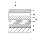
- FIG. 6 shows a configuration of the variable resistance element 13 according to the second comparative example.
- the variable resistance element 13 is formed on the substrate 2 with the lower electrode layer 3, the first metal oxide layer 51, The second metal oxide layer 52, the current limiting layer 40, and the upper electrode layer 6 are stacked in this order.
- the current limiting layer 40 has the same configuration as the current limiting layer 4 shown in FIG.
- the Schottky barrier is represented by the symbol b2 in FIG. As shown. In this case, the resistance change element 13 shown in FIG. 6 has a low resistance value in the high resistance state, and it is difficult to maintain a stable high resistance state.
- variable resistance element 13 when a negative voltage is applied to the upper electrode layer 6 for data writing, oxygen ions in the current limiting layer 40 and the second metal oxide layer 52 are the first. It moves to the metal oxide layer 51 side. In this case, the amount of oxygen ions required for changing the resistance increases by the amount of the current limiting layer 40, and the resistance change does not appear unless a large voltage is applied.
- the oxygen ions in the second metal oxide layer 52 move to the current limiting layer 40, and this does not occur in normal switching operation. Operation occurs, and switching reliability decreases.
- the current limiting layer 4 is inserted between the lower electrode layer 3 (BE-Pt) and the first metal oxide layer 51 (TaOx).
- a high potential barrier between the upper electrode layer 6 and the second metal oxide layer 52 is ensured.
- the high resistance state can be stably maintained, and a highly reliable switching operation can be ensured.
- the current limiting layer 4 is formed of a metal oxide layer.
- the current limiting layer 4 may be formed of other materials, for example, an oxide film of the lower electrode layer 3. It may be configured. Thereby, the same effect as the above-mentioned 1st Embodiment can be acquired.
- the second metal oxide layer 52 having a higher resistivity than the first metal oxide layer 51 is joined to the upper electrode layer 6.
- the second metal oxide layer 52 is joined.
- the physical layer 52 may be bonded to the lower electrode layer 3.
- the current limiting layer 4 is disposed between the first metal oxide layer 51 and the upper electrode layer 6.
Landscapes
- Engineering & Computer Science (AREA)
- Chemical & Material Sciences (AREA)
- Microelectronics & Electronic Packaging (AREA)
- Manufacturing & Machinery (AREA)
- Chemical Kinetics & Catalysis (AREA)
- Materials Engineering (AREA)
- Mechanical Engineering (AREA)
- Metallurgy (AREA)
- Organic Chemistry (AREA)
- Physics & Mathematics (AREA)
- Electromagnetism (AREA)
- Semiconductor Memories (AREA)
Abstract
Description
上記第1の金属酸化物層は、上記第1の電極と上記第2の電極との間に配置され、第1の抵抗率を有する。
上記第2の金属酸化物層は、上記第1の金属酸化物層と上記第2の電極との間に配置され、上記第1の抵抗率よりも高い第2の抵抗率を有する。
上記電流制限層は、上記第1の電極と上記第1の金属酸化物層との間に配置され、上記第1の抵抗率よりも高く上記第2の抵抗率よりも低い第3の抵抗率を有する。
上記第1の電極の上に、第1の抵抗率よりも高く第2の抵抗率よりも低い第3の抵抗率を有する金属酸化物で構成された電流制限層が形成される。
上記電流制限層の上に、上記第1の抵抗率を有する第1の金属酸化物層が形成される。
上記第1の金属酸化物層の上に、上記第2の抵抗率を有する第2の金属酸化物層が形成される。
上記第2の金属酸化物層の上に、第2の電極が形成される。
上記第1の金属酸化物層は、上記第1の電極と上記第2の電極との間に配置され、第1の抵抗率を有する。
上記第2の金属酸化物層は、上記第1の金属酸化物層と上記第2の電極との間に配置され、上記第1の抵抗率よりも高い第2の抵抗率を有する。
上記電流制限層は、上記第1の電極と上記第1の金属酸化物層との間に配置され、上記第1の抵抗率よりも高く上記第2の抵抗率よりも低い第3の抵抗率を有する。
これにより第1及び第2の金属酸化物層と同様の成膜装置で電流制限層を形成することができ、生産性の低下を抑制することができる。
また上記電流制限層は、上記第1の電極に対してオーミック接合されることで、高抵抗状態と低抵抗状態との間の安定した状態遷移、すなわちスイッチング動作を確保することができる。
これにより抵抗率の異なる第1及び第2の金属酸化物層を容易に形成することができる。
上記第1の電極の上に、第1の抵抗率よりも高く第2の抵抗率よりも低い第3の抵抗率を有する金属酸化物で構成された電流制限層が形成される。
上記電流制限層の上に、上記第1の抵抗率を有する第1の金属酸化物層が形成される。
上記第1の金属酸化物層の上に、上記第2の抵抗率を有する第2の金属酸化物層が形成される。
上記第2の金属酸化物層の上に、第2の電極が形成される。
(1)金属酸化物ターゲットとArなどの不活性ガスを用いた高周波スパッタ法により、金属酸化物層を形成する。
(2)Pt,Ir,Ru,Pd,TiN,TiAlN,TaNなどの酸化耐性がある電極上にALD法、CVD法、酸化ガスによる反応性スパッタ法などにより、金属酸化物を多層積層する。
(3)IrOx,RuOx,SrRuO3,LaNiO3,ITOなどの酸化物電気伝導体上にALD法、CVD法、酸化ガスによる反応性スパッタ法などにより、金属酸化物を堆積させる。
(4)TaC,WSi,WGeのようなSi,C,Geなどの還元力の強い元素が含まれる電気伝導体上にALD法、CVD法、酸化ガスによる反応性スパッタ法などにより、金属酸化物を堆積させる。
(5)電位障壁を形成しない金属材料と酸化物材料を組み合わせる。
2…基板
3…下部電極層
4…電流制限層
5…酸化物半導体層
6…上部電極層
51…第1の金属酸化物層
52…第2の金属酸化物層
Claims (6)
- 第1の電極と、
第2の電極と、
前記第1の電極と前記第2の電極との間に配置され、第1の抵抗率を有する第1の金属酸化物層と、
前記第1の金属酸化物層と前記第2の電極との間に配置され、前記第1の抵抗率よりも高い第2の抵抗率を有する第2の金属酸化物層と、
前記第1の電極と前記第1の金属酸化物層との間に配置され、前記第1の抵抗率よりも高く前記第2の抵抗率よりも低い第3の抵抗率を有する電流制限層と
を具備する抵抗変化素子。 - 請求項1に記載の抵抗変化素子であって、
前記電流制限層は、金属酸化物で構成される
抵抗変化素子。 - 請求項1又は2に記載の抵抗変化素子であって、
前記電流制限層は、酸素欠損した金属酸化物で構成され、前記第1の電極に対してオーミック接合される
抵抗変化素子。 - 請求項1から3のいずれか1項に記載の抵抗変化素子であって、
前記第1の金属酸化物層は、酸素欠損した金属酸化物で構成され、
前記第2の金属酸化物層は、化学量論組成の金属酸化物で構成される
抵抗変化素子。 - 第1の電極を形成し、
前記第1の電極の上に、第1の抵抗率よりも高く第2の抵抗率よりも低い第3の抵抗率を有する金属酸化物で構成された電流制限層を形成し、
前記電流制限層の上に、前記第1の抵抗率を有する第1の金属酸化物層を形成し、
前記第1の金属酸化物層の上に、前記第2の抵抗率を有する第2の金属酸化物層を形成し、
前記第2の金属酸化物層の上に、第2の電極を形成する
抵抗変化素子の製造方法。 - 請求項5に記載の抵抗変化素子の製造方法であって、
前記電流制限層、前記第1の金属酸化物層及び前記第2の金属酸化物層は、酸素雰囲気中での反応性スパッタリング法によって形成される
抵抗変化素子の製造方法。
Priority Applications (5)
| Application Number | Priority Date | Filing Date | Title |
|---|---|---|---|
| KR1020147009144A KR20140068162A (ko) | 2012-09-05 | 2013-08-27 | 저항 변화 소자 및 그 제조 방법 |
| US14/369,659 US9343207B2 (en) | 2012-09-05 | 2013-08-27 | Resistance change device, and method for producing same |
| JP2014534171A JP5696260B2 (ja) | 2012-09-05 | 2013-08-27 | 抵抗変化素子及びその製造方法 |
| KR1020157033560A KR101607820B1 (ko) | 2012-09-05 | 2013-08-27 | 저항 변화 소자 및 그 제조 방법 |
| CN201380003674.0A CN103907187B (zh) | 2012-09-05 | 2013-08-27 | 电阻转变元件及其制作方法 |
Applications Claiming Priority (2)
| Application Number | Priority Date | Filing Date | Title |
|---|---|---|---|
| JP2012194823 | 2012-09-05 | ||
| JP2012-194823 | 2012-09-05 |
Publications (1)
| Publication Number | Publication Date |
|---|---|
| WO2014038152A1 true WO2014038152A1 (ja) | 2014-03-13 |
Family
ID=50236786
Family Applications (1)
| Application Number | Title | Priority Date | Filing Date |
|---|---|---|---|
| PCT/JP2013/005044 Ceased WO2014038152A1 (ja) | 2012-09-05 | 2013-08-27 | 抵抗変化素子及びその製造方法 |
Country Status (6)
| Country | Link |
|---|---|
| US (1) | US9343207B2 (ja) |
| JP (1) | JP5696260B2 (ja) |
| KR (2) | KR20140068162A (ja) |
| CN (1) | CN103907187B (ja) |
| TW (1) | TWI584470B (ja) |
| WO (1) | WO2014038152A1 (ja) |
Cited By (1)
| Publication number | Priority date | Publication date | Assignee | Title |
|---|---|---|---|---|
| JP2016225605A (ja) * | 2015-06-01 | 2016-12-28 | 華邦電子股▲ふん▼有限公司 | 抵抗性ランダムアクセスメモリ |
Families Citing this family (16)
| Publication number | Priority date | Publication date | Assignee | Title |
|---|---|---|---|---|
| US10147762B2 (en) * | 2014-06-26 | 2018-12-04 | Hewlett Packard Enterprise Development Lp | Protective elements for non-volatile memory cells in crossbar arrays |
| US10611161B2 (en) | 2014-07-24 | 2020-04-07 | Avision Inc. | Image forming agent storage member and laser printer using the same |
| TWI559519B (zh) * | 2015-02-16 | 2016-11-21 | 國立清華大學 | 電阻式記憶體 |
| JP2018160547A (ja) | 2017-03-22 | 2018-10-11 | 東芝メモリ株式会社 | 記憶装置 |
| WO2018193759A1 (ja) * | 2017-04-18 | 2018-10-25 | 株式会社アルバック | 抵抗変化素子の製造方法及び抵抗変化素子 |
| US10516106B2 (en) * | 2017-06-26 | 2019-12-24 | Taiwan Semiconductor Manufacturing Co., Ltd. | Electrode structure to improve RRAM performance |
| JP7359876B2 (ja) | 2019-06-12 | 2023-10-11 | アプライド マテリアルズ インコーポレイテッド | ニューロモルフィックスイッチング用の二重酸化物アナログスイッチ |
| KR102286867B1 (ko) | 2019-09-17 | 2021-08-06 | 아주대학교산학협력단 | 저항 스위칭 소자 및 이를 포함하는 메모리 장치 |
| US12213390B2 (en) | 2021-05-12 | 2025-01-28 | Tetramem Inc. | Resistive random-access memory devices with multi-component electrodes |
| US12302768B2 (en) | 2021-05-12 | 2025-05-13 | Tetramem Inc. | Resistive random-access memory devices with multi-component electrodes |
| US12396375B2 (en) | 2020-07-06 | 2025-08-19 | Tetramem Inc. | Resistive random-access memory devices with engineered electronic defects and methods for making the same |
| US11527712B2 (en) * | 2020-07-06 | 2022-12-13 | Tetramem Inc. | Low current RRAM-based crossbar array circuits implemented with interface engineering technologies |
| US12382847B2 (en) | 2020-07-06 | 2025-08-05 | Tetramem Inc. | Resistive random-access memory devices with multi-component electrodes and discontinuous interface layers |
| CN114365299B (zh) | 2020-08-07 | 2025-09-19 | 合肥睿科微电子有限公司 | 具有防止存储器件内形成空洞的改进式存储器单元结构的存储器件 |
| US12543514B2 (en) | 2021-05-12 | 2026-02-03 | Tetramem Inc. | Resistive random-access memory devices with metal-nitride compound electrodes |
| KR102892176B1 (ko) * | 2024-03-29 | 2025-12-01 | 한국과학기술연구원 | 다층 구조의 저항 변화 메모리 기반 멤리스터 소자 및 그 제조 방법 |
Citations (4)
| Publication number | Priority date | Publication date | Assignee | Title |
|---|---|---|---|---|
| WO2009125777A1 (ja) * | 2008-04-07 | 2009-10-15 | 日本電気株式会社 | 抵抗変化素子及びその製造方法 |
| US20100038791A1 (en) * | 2008-08-12 | 2010-02-18 | Industrial Technology Research Institute | Resistive random access memory and method for fabricating the same |
| WO2012046454A1 (ja) * | 2010-10-08 | 2012-04-12 | パナソニック株式会社 | 不揮発性記憶素子およびその製造方法 |
| WO2012169195A1 (ja) * | 2011-06-10 | 2012-12-13 | 株式会社アルバック | 抵抗変化素子及びその製造方法 |
Family Cites Families (13)
| Publication number | Priority date | Publication date | Assignee | Title |
|---|---|---|---|---|
| US6682772B1 (en) * | 2000-04-24 | 2004-01-27 | Ramtron International Corporation | High temperature deposition of Pt/TiOx for bottom electrodes |
| JPWO2006080276A1 (ja) * | 2005-01-28 | 2008-06-19 | 株式会社アルバック | キャパシタンス素子製造方法、エッチング方法 |
| KR101176543B1 (ko) * | 2006-03-10 | 2012-08-28 | 삼성전자주식회사 | 저항성 메모리소자 |
| CN101542730B (zh) * | 2007-06-05 | 2011-04-06 | 松下电器产业株式会社 | 非易失性存储元件和其制造方法、以及使用了该非易失性存储元件的非易失性半导体装置 |
| WO2009050833A1 (ja) * | 2007-10-15 | 2009-04-23 | Panasonic Corporation | 不揮発性記憶素子、並びにその不揮発性記憶素子を用いた不揮発性半導体装置 |
| JP2009135370A (ja) * | 2007-12-03 | 2009-06-18 | Panasonic Corp | 不揮発性記憶素子およびその製造方法、並びにその不揮発性記憶素子を用いた不揮発性半導体装置 |
| CN101978496B (zh) * | 2008-07-11 | 2012-11-07 | 松下电器产业株式会社 | 非易失性存储元件和其制造方法、以及使用该非易失性存储元件的非易失性半导体装置 |
| JP4643767B2 (ja) | 2009-04-15 | 2011-03-02 | パナソニック株式会社 | 抵抗変化型不揮発性記憶装置 |
| WO2011030559A1 (ja) | 2009-09-14 | 2011-03-17 | パナソニック株式会社 | 不揮発性記憶装置及びその製造方法 |
| JPWO2011043448A1 (ja) * | 2009-10-09 | 2013-03-04 | 日本電気株式会社 | 半導体装置及びその製造方法 |
| JP5001464B2 (ja) * | 2010-03-19 | 2012-08-15 | パナソニック株式会社 | 不揮発性記憶素子、その製造方法、その設計支援方法および不揮発性記憶装置 |
| KR101744758B1 (ko) | 2010-08-31 | 2017-06-09 | 삼성전자 주식회사 | 비휘발성 메모리요소 및 이를 포함하는 메모리소자 |
| JP2013004655A (ja) * | 2011-06-15 | 2013-01-07 | Sharp Corp | 不揮発性半導体記憶装置およびその製造方法 |
-
2013
- 2013-08-27 KR KR1020147009144A patent/KR20140068162A/ko not_active Ceased
- 2013-08-27 JP JP2014534171A patent/JP5696260B2/ja active Active
- 2013-08-27 KR KR1020157033560A patent/KR101607820B1/ko active Active
- 2013-08-27 WO PCT/JP2013/005044 patent/WO2014038152A1/ja not_active Ceased
- 2013-08-27 CN CN201380003674.0A patent/CN103907187B/zh active Active
- 2013-08-27 US US14/369,659 patent/US9343207B2/en active Active
- 2013-09-04 TW TW102131888A patent/TWI584470B/zh active
Patent Citations (4)
| Publication number | Priority date | Publication date | Assignee | Title |
|---|---|---|---|---|
| WO2009125777A1 (ja) * | 2008-04-07 | 2009-10-15 | 日本電気株式会社 | 抵抗変化素子及びその製造方法 |
| US20100038791A1 (en) * | 2008-08-12 | 2010-02-18 | Industrial Technology Research Institute | Resistive random access memory and method for fabricating the same |
| WO2012046454A1 (ja) * | 2010-10-08 | 2012-04-12 | パナソニック株式会社 | 不揮発性記憶素子およびその製造方法 |
| WO2012169195A1 (ja) * | 2011-06-10 | 2012-12-13 | 株式会社アルバック | 抵抗変化素子及びその製造方法 |
Cited By (2)
| Publication number | Priority date | Publication date | Assignee | Title |
|---|---|---|---|---|
| JP2016225605A (ja) * | 2015-06-01 | 2016-12-28 | 華邦電子股▲ふん▼有限公司 | 抵抗性ランダムアクセスメモリ |
| US10157962B2 (en) | 2015-06-01 | 2018-12-18 | Winbond Electronics Corp. | Resistive random access memory |
Also Published As
| Publication number | Publication date |
|---|---|
| KR101607820B1 (ko) | 2016-03-30 |
| CN103907187B (zh) | 2016-04-13 |
| TWI584470B (zh) | 2017-05-21 |
| KR20150138423A (ko) | 2015-12-09 |
| KR20140068162A (ko) | 2014-06-05 |
| JPWO2014038152A1 (ja) | 2016-08-08 |
| US9343207B2 (en) | 2016-05-17 |
| JP5696260B2 (ja) | 2015-04-08 |
| TW201423985A (zh) | 2014-06-16 |
| CN103907187A (zh) | 2014-07-02 |
| US20140361864A1 (en) | 2014-12-11 |
Similar Documents
| Publication | Publication Date | Title |
|---|---|---|
| JP5696260B2 (ja) | 抵抗変化素子及びその製造方法 | |
| JP5152173B2 (ja) | 半導体装置及びその製造方法 | |
| JP5468087B2 (ja) | 不揮発性記憶素子及び不揮発性記憶装置 | |
| JP5154138B2 (ja) | n+界面層を備えた可変抵抗ランダムアクセスメモリ素子 | |
| US8675393B2 (en) | Method for driving non-volatile memory element, and non-volatile memory device | |
| JP4948688B2 (ja) | 抵抗変化型不揮発性記憶素子、抵抗変化型不揮発性記憶装置及び抵抗変化型不揮発性記憶素子の製造方法 | |
| JP5524296B2 (ja) | 記憶素子及び記憶装置 | |
| JP5148025B2 (ja) | 不揮発性半導体記憶素子の製造方法 | |
| CN103222055B (zh) | 非易失性存储元件及其制造方法 | |
| CN103597597B (zh) | 可变电阻元件及其制造方法 | |
| KR20090126530A (ko) | 저항성 메모리 소자 | |
| US9252189B2 (en) | Nonvolatile semiconductor memory element, nonvolatile semiconductor memory device, and method for manufacturing nonvolatile semiconductor memory device | |
| JP5074583B2 (ja) | 不揮発性記憶素子の製造方法、および不揮発性記憶装置の製造方法 | |
| KR102464065B1 (ko) | 스위칭 소자, 이의 제조 방법, 스위칭 소자를 선택 소자로서 포함하는 저항 변화 메모리 장치 | |
| US9105332B2 (en) | Variable resistance nonvolatile memory device | |
| JP4939414B2 (ja) | 可変抵抗素子 | |
| JP2013207131A (ja) | 抵抗変化素子及びその製造方法 | |
| WO2012102025A1 (ja) | 不揮発性記憶装置 | |
| JP2014175419A (ja) | 電流制御素子、不揮発性記憶素子、不揮発性記憶装置および電流制御素子の製造方法 | |
| CN103180948B (zh) | 非易失性存储元件、非易失性存储装置及非易失性存储元件的写入方法 |
Legal Events
| Date | Code | Title | Description |
|---|---|---|---|
| ENP | Entry into the national phase |
Ref document number: 20147009144 Country of ref document: KR Kind code of ref document: A |
|
| ENP | Entry into the national phase |
Ref document number: 2014534171 Country of ref document: JP Kind code of ref document: A |
|
| 121 | Ep: the epo has been informed by wipo that ep was designated in this application |
Ref document number: 13835973 Country of ref document: EP Kind code of ref document: A1 |
|
| WWE | Wipo information: entry into national phase |
Ref document number: 14369659 Country of ref document: US |
|
| NENP | Non-entry into the national phase |
Ref country code: DE |
|
| 122 | Ep: pct application non-entry in european phase |
Ref document number: 13835973 Country of ref document: EP Kind code of ref document: A1 |