WO2014034720A1 - 防眩・反射防止部材及びその製造方法 - Google Patents
防眩・反射防止部材及びその製造方法 Download PDFInfo
- Publication number
- WO2014034720A1 WO2014034720A1 PCT/JP2013/073000 JP2013073000W WO2014034720A1 WO 2014034720 A1 WO2014034720 A1 WO 2014034720A1 JP 2013073000 W JP2013073000 W JP 2013073000W WO 2014034720 A1 WO2014034720 A1 WO 2014034720A1
- Authority
- WO
- WIPO (PCT)
- Prior art keywords
- layer
- antiglare
- antireflection
- antireflection member
- member according
- Prior art date
- Legal status (The legal status is an assumption and is not a legal conclusion. Google has not performed a legal analysis and makes no representation as to the accuracy of the status listed.)
- Ceased
Links
Images
Classifications
-
- B—PERFORMING OPERATIONS; TRANSPORTING
- B32—LAYERED PRODUCTS
- B32B—LAYERED PRODUCTS, i.e. PRODUCTS BUILT-UP OF STRATA OF FLAT OR NON-FLAT, e.g. CELLULAR OR HONEYCOMB, FORM
- B32B17/00—Layered products essentially comprising sheet glass, or glass, slag, or like fibres
- B32B17/06—Layered products essentially comprising sheet glass, or glass, slag, or like fibres comprising glass as the main or only constituent of a layer, next to another layer of a specific material
- B32B17/10—Layered products essentially comprising sheet glass, or glass, slag, or like fibres comprising glass as the main or only constituent of a layer, next to another layer of a specific material of synthetic resin
-
- G—PHYSICS
- G02—OPTICS
- G02B—OPTICAL ELEMENTS, SYSTEMS OR APPARATUS
- G02B1/00—Optical elements characterised by the material of which they are made; Optical coatings for optical elements
- G02B1/10—Optical coatings produced by application to, or surface treatment of, optical elements
- G02B1/11—Anti-reflection coatings
- G02B1/118—Anti-reflection coatings having sub-optical wavelength surface structures designed to provide an enhanced transmittance, e.g. moth-eye structures
-
- B—PERFORMING OPERATIONS; TRANSPORTING
- B24—GRINDING; POLISHING
- B24C—ABRASIVE OR RELATED BLASTING WITH PARTICULATE MATERIAL
- B24C1/00—Methods for use of abrasive blasting for producing particular effects; Use of auxiliary equipment in connection with such methods
- B24C1/06—Methods for use of abrasive blasting for producing particular effects; Use of auxiliary equipment in connection with such methods for producing matt surfaces, e.g. on plastic materials, on glass
-
- B—PERFORMING OPERATIONS; TRANSPORTING
- B32—LAYERED PRODUCTS
- B32B—LAYERED PRODUCTS, i.e. PRODUCTS BUILT-UP OF STRATA OF FLAT OR NON-FLAT, e.g. CELLULAR OR HONEYCOMB, FORM
- B32B7/00—Layered products characterised by the relation between layers; Layered products characterised by the relative orientation of features between layers, or by the relative values of a measurable parameter between layers, i.e. products comprising layers having different physical, chemical or physicochemical properties; Layered products characterised by the interconnection of layers
- B32B7/02—Physical, chemical or physicochemical properties
-
- G—PHYSICS
- G02—OPTICS
- G02B—OPTICAL ELEMENTS, SYSTEMS OR APPARATUS
- G02B1/00—Optical elements characterised by the material of which they are made; Optical coatings for optical elements
- G02B1/10—Optical coatings produced by application to, or surface treatment of, optical elements
- G02B1/11—Anti-reflection coatings
-
- G—PHYSICS
- G02—OPTICS
- G02B—OPTICAL ELEMENTS, SYSTEMS OR APPARATUS
- G02B1/00—Optical elements characterised by the material of which they are made; Optical coatings for optical elements
- G02B1/10—Optical coatings produced by application to, or surface treatment of, optical elements
- G02B1/11—Anti-reflection coatings
- G02B1/111—Anti-reflection coatings using layers comprising organic materials
-
- G—PHYSICS
- G02—OPTICS
- G02B—OPTICAL ELEMENTS, SYSTEMS OR APPARATUS
- G02B1/00—Optical elements characterised by the material of which they are made; Optical coatings for optical elements
- G02B1/10—Optical coatings produced by application to, or surface treatment of, optical elements
- G02B1/11—Anti-reflection coatings
- G02B1/113—Anti-reflection coatings using inorganic layer materials only
- G02B1/115—Multilayers
-
- G—PHYSICS
- G02—OPTICS
- G02B—OPTICAL ELEMENTS, SYSTEMS OR APPARATUS
- G02B1/00—Optical elements characterised by the material of which they are made; Optical coatings for optical elements
- G02B1/10—Optical coatings produced by application to, or surface treatment of, optical elements
- G02B1/12—Optical coatings produced by application to, or surface treatment of, optical elements by surface treatment, e.g. by irradiation
-
- G—PHYSICS
- G02—OPTICS
- G02B—OPTICAL ELEMENTS, SYSTEMS OR APPARATUS
- G02B1/00—Optical elements characterised by the material of which they are made; Optical coatings for optical elements
- G02B1/10—Optical coatings produced by application to, or surface treatment of, optical elements
- G02B1/18—Coatings for keeping optical surfaces clean, e.g. hydrophobic or photo-catalytic films
-
- G—PHYSICS
- G02—OPTICS
- G02B—OPTICAL ELEMENTS, SYSTEMS OR APPARATUS
- G02B5/00—Optical elements other than lenses
- G02B5/02—Diffusing elements; Afocal elements
- G02B5/0273—Diffusing elements; Afocal elements characterized by the use
- G02B5/0294—Diffusing elements; Afocal elements characterized by the use adapted to provide an additional optical effect, e.g. anti-reflection or filter
-
- B—PERFORMING OPERATIONS; TRANSPORTING
- B32—LAYERED PRODUCTS
- B32B—LAYERED PRODUCTS, i.e. PRODUCTS BUILT-UP OF STRATA OF FLAT OR NON-FLAT, e.g. CELLULAR OR HONEYCOMB, FORM
- B32B2307/00—Properties of the layers or laminate
- B32B2307/40—Properties of the layers or laminate having particular optical properties
- B32B2307/416—Reflective
Definitions
- the present invention relates to an antiglare / antireflection member and a method for producing the same.
- Patent Document 1 provides an antireflection layer having both an antireflection function and an antiglare function, in which an antireflection layer composed of a low refractive index layer is provided on a substrate and the surface of the low refractive index layer is antiglare treated. Is described.
- the main object of the present invention is to provide an antiglare / antireflection member having excellent visibility.
- the antiglare / antireflection member according to the present invention includes a base material and an antireflection layer.
- An antiglare layer having a concavo-convex structure is provided on the surface layer of the substrate.
- the antireflection layer is provided on the antiglare layer.
- the base material may have a base material body and an island layer that is disposed on the base material body and constitutes an antiglare layer.
- the base body may be composed of a resin film, a glass film, a resin plate, or a glass plate.
- the antiglare / antireflection member according to the present invention preferably further includes an antireflection layer provided on the surface of the base material opposite to the antireflection layer.
- the antireflection layer may be composed of a low refractive index layer having a lower refractive index than the base material.
- the antireflection layer may be formed by alternately laminating a low refractive index layer having a relatively low refractive index and a high refractive index layer having a relatively high refractive index.
- An antifouling layer containing fluorine may be further provided on the antireflection layer.
- the first method for producing an antiglare / antireflection member according to the present invention relates to a method for producing the above antiglare / antireflection member.
- An island-shaped layer is formed by applying a light-transmitting material on the surface of the light-transmitting plate by a spray method, and a base material including the light-transmitting plate and the island-shaped layer is manufactured.
- the second method for producing an antiglare / antireflection member according to the present invention relates to a method for producing the above antiglare / antireflection member.
- a base material is produced by blasting the surface of the translucent plate to form an uneven structure.
- an antiglare / antireflection member In the second method of manufacturing an antiglare / antireflection member according to the present invention, it is preferable to perform etching after blasting the surface of the light transmitting plate.
- an antiglare / antireflection member having excellent visibility can be provided.
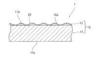
- FIG. 1 is a schematic cross-sectional view of an antiglare / antireflection member according to an embodiment of the present invention.
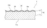
- FIG. 2 is a schematic cross-sectional view of an antiglare / antireflection member according to another embodiment of the present invention.
- FIG. 1 is a schematic cross-sectional view of an antiglare / antireflection member according to this embodiment.
- the antiglare / antireflection member 1 shown in FIG. 1 is a member for improving the visibility of the display device, for example, disposed on the display surface of the display device.
- the antiglare / antireflection member 1 may be a film-like member attached on the display surface of the display device, or may be a member constituting a front plate of the display device. That is, it may be a member that is attached to the display device afterwards, or may be one of the constituent members of the display device.
- the antiglare / antireflection member 1 has a base material 10. On the surface layer of the base material 10, an antiglare layer 10a having an uneven structure and having an antiglare function is provided. Specifically, in the present embodiment, the substrate 10 includes a substrate body 11 and an island layer 12.
- the constituent material of the base body 11 is not particularly limited as long as it is a translucent member.
- the base body 11 can be composed of, for example, a resin film, a glass film, a resin plate, or a glass plate.
- the glass plate can be composed of, for example, an alkali-free glass substrate, a soda lime glass substrate, a chemically strengthened glass substrate, or the like.
- the base body 11 has a first main surface 11a facing the display device side and a second main surface 11b facing the viewer side in the usage state of the anti-glare / antireflection member 1.
- the 1st and 2nd main surfaces 11a and 11b are each comprised by the flat surface.
- the island layer 12 is provided on the second main surface 11b. This island layer 12 constitutes an antiglare layer 10a.
- the island layer 12 is a layer provided in an island shape.
- the concavo-convex structure is formed by providing the island-like layer 12 covering a part of the second main surface 11b.
- the concavo-convex structure preferably has no regularity. This is because the antiglare function of the antiglare layer 10a is improved.
- the constituent material of the island layer 12 is not particularly limited as long as it has translucency and is in close contact with the base body 11.
- the island layer 12 can be made of, for example, SiO 2 , TiO 2 , Al 2 O 3 , ZrO 2, or the like.
- An antireflection layer 20 is provided on the antiglare layer 10a. Therefore, the antireflection layer 20 is provided on the concavo-convex structure.
- the antireflection layer 20 is a layer having a function of reducing the surface reflectance.
- the antireflection layer 20 may be any layer that has a lower surface reflectance when the antireflection layer 20 is provided than when the antireflection layer 20 is not provided, and the surface reflectance is zero. There is no necessity.
- the antireflection layer 20 may be composed of, for example, a low refractive index layer having a refractive index lower than that of the substrate 10. Further, the antireflection layer 20 may be composed of a dielectric multilayer film in which a low refractive index layer having a relatively low refractive index and a high refractive index layer having a relatively high refractive index are alternately laminated.
- the reflection suppressing function of the antireflection layer largely depends on the thickness of the antireflection layer. For this reason, the reflection suppressing function is generally provided on a flat surface. Therefore, for example, when an antiglare layer and an antireflection layer are provided, it is considered necessary to first form an antireflection layer on the flat surface of the substrate and then form an antiglare layer on the antireflection layer. It was done.
- the visibility of the display device can be further improved by providing the antireflection layer 20 on the antiglare layer 10a having an uneven structure. That is, the present inventors have found that a sufficient antireflection function can be obtained even when the antireflection layer 20 is disposed on the antiglare layer 10a.
- the antiglare layer 10a since the antiglare layer 10a is provided, excellent antiglare properties can be obtained. Furthermore, since the antireflection layer 20 is disposed on the antiglare layer 10a, the reflectance in the antiglare layer 10a is reduced. Therefore, the amount of light irregularly reflected by the antiglare layer 10a can be reduced. Therefore, more excellent antiglare properties can be obtained.
- the antireflection layer 20 is provided on the outermost layer on the viewer side, the reflection of the background can be reduced.
- the antiglare / antireflection member 1 when used, excellent antiglare properties can be realized while suppressing the reflection of the background. Therefore, the visibility of the display device can be improved by using the antiglare / antireflection member 1.
- Another layer having a thickness that does not impair the function of the antireflection layer 20 may be formed on the antireflection layer 20.
- an antifouling layer 30 containing fluorine having a thickness of 200 nm or less may be formed on the antireflection layer 20.
- the antifouling layer 30 containing fluorine may be, for example, a polymer having —Si—O—Si— bonds (siloxane bonds) and water-repellent functional groups containing fluorine.
- the siloxane bond is synthesized by dehydration condensation of two molecules of silanol.
- the antiglare / antireflection member 1 may be provided with a pressure-sensitive adhesive layer or an adhesive layer on the first main surface 11a.
- the antiglare / antireflection member 1 can be adhered or adhered to a display screen such as a liquid crystal display through the adhesive layer or the adhesive layer.
- the antiglare / antireflection member 1 can be manufactured, for example, in the following manner. First, on the base material body 11 as a translucent plate made of glass or resin, for example, a translucent material is applied by a spray method and dried to form an island-like layer 12 to produce the base material 10. . Then, the anti-glare / antireflection member 1 can be manufactured by forming the antireflection layer 20 on the island layer 12 of the substrate 10.
- the antireflection layer 20 can be formed by, for example, a sputtering method or a CVD (Chemical Vapor Deposition) method.
- the base material 10 can also be produced, for example, by blasting the surface of the light-transmitting plate to form an uneven structure. In this case, it is preferable to etch the surface after blasting. For example, when the substrate is made of a thin glass plate or glass film, the substrate may be damaged by the blast treatment, and therefore, it is preferable to form the antiglare layer 10a using a spray method.
- Example 1 An anti-glare layer made of SiO 2 and having an uneven structure on a non-alkali glass OA-10G substrate manufactured by Nippon Electric Glass Co., Ltd. having a thickness of 0.5 mm and a surface roughness (Ra) of about 0.2 nm. Formed. The average thickness of the antiglare layer was about 500 nm. The antiglare layer had a haze value of about 12.
- the resulting antiglare / antireflection member was evaluated for reflection of outside scenes and contrast by the following method. The results are shown in Table 1.
- the contrast was evaluated by placing an antiglare / antireflection member on the liquid crystal screen and observing the image on the liquid crystal screen through the antiglare / antireflection member. Specifically, “ ⁇ ” indicates that the image appears clearer than when the LCD screen is observed as it is, “ ⁇ ” indicates that the image is as clear as when the LCD screen is observed as it is, and “LCD” The case where it was seen more blurred than when observed as it was was evaluated as “x”.
- Example 1 Comparative Example 1 In the same manner as in Example 1, only the antiglare layer was formed on the substrate, and no antireflection layer was provided. The resulting member was evaluated for reflection of the outside scene and contrast in the same manner as in Example 1. The results are shown in Table 1.
- Example 2 In the same manner as in Example 1, only the antireflection layer was formed on the substrate, and no antiglare layer was provided. The resulting member was evaluated for reflection of the outside scene and contrast in the same manner as in Example 1. The results are shown in Table 1.
- Example 1 there was almost no reflection of the outside scene and the contrast was good.
- Comparative Example 1 the reflection of the outside scene was only slightly confirmed, but the contrast was greatly reduced.
- Comparative Example 2 the contrast was good, but the reflection of the outside scene was insufficient.
- Example 2 A glass substrate having a thickness of 0.7 mm, a surface roughness (Ra) of about 0.2 nm, and a thermal expansion coefficient of 102 ⁇ 10 ⁇ 7 / ° C. is made of SiO 2 and has a concavo-convex structure using a spray method. An antiglare layer was formed. The average thickness of the antiglare layer was about 200 nm. The antiglare layer had a haze value of about 6.5.
- Example 2 Evaluation of reflection and contrast of outside scene was performed on the obtained antiglare and antireflection member.
- Example 1 For the reflection of the outside scene, the same evaluation as in Example 1 was performed.
- the contrast was evaluated in the same manner as in Example 1 except that an antiglare / antireflection member was placed on the liquid crystal screen with a gap of 2.5 mm between the screen and the screen.
- Example 2 As a result, in Example 2, as in Example 1, almost no reflection of the outside scene could be confirmed ()), and it looked as clear as when the liquid crystal screen was observed as it was ( ⁇ ).
- the thermal expansion coefficient of the antiglare / antireflection member and the thermal expansion coefficient of the liquid crystal screen are not always the same. If the thermal expansion coefficient of the antiglare / antireflection member is different from the thermal expansion coefficient of the liquid crystal screen, the antiglare / antireflection member and the liquid crystal screen are brought into close contact with each other when the temperature changes. Stress is applied to the glare / reflection preventing member and the liquid crystal screen. For this reason, there is a case where it is desired to arrange the antiglare / antireflection member and the liquid crystal screen apart from each other. However, when a gap is provided between the antiglare / antireflection member and the liquid crystal screen, the contrast usually tends to decrease.
- an antireflection layer is provided on the antiglare layer and an antireflection layer is provided on the surface opposite to the antiglare layer of the substrate as in Example 2, antiglare / antireflection Even if there was a gap between the member and the liquid crystal screen, the contrast was good. From the viewpoint of obtaining good contrast, an antireflection layer is provided on the antiglare layer as in Example 2, and an antireflection layer is also provided on the surface of the substrate opposite to the antiglare layer. preferable.
- Example 3 On the antireflection layer of the antiglare / antireflection member obtained in the same manner as in Example 1, an antifouling layer was provided as follows.
- a fluorine-based coating agent manufactured by Daikin, Optool DSX (registered trademark) was applied and dried to form an antifouling layer.
- the thickness of the antifouling layer was about 20 nm.
- the obtained antiglare / antireflection member has an antiglare layer formed on the substrate, an antireflection layer formed on the antiglare layer, and an antifouling layer formed on the antireflection layer.
- Example 2 Evaluation of reflection and contrast of outside scene was performed on the obtained antiglare and antireflection member.
- the same evaluation as in Example 1 was performed. Contrast was evaluated in the same manner as in Example 1 except that an adhesive layer was applied on the first main surface and adhered to the liquid crystal screen via the adhesive layer.
- an adhesive KE1051J A / B manufactured by Shin-Etsu Chemical Co., Ltd. was used, and the thickness of the adhesive layer was 5 ⁇ m.
- Example 3 As a result, also in Example 3, as in Examples 1 and 2, almost no reflection of the outside scene could be confirmed ( ⁇ ), and it seemed as clear as when the liquid crystal screen was observed as it was ()).
- the peel resistance of the antifouling layer was evaluated as follows. Regarding the anti-fouling property of the antifouling layer, steel wool # 0000 was placed on the antifouling layer, and a load of 500 gf / cm 2 was applied to the steel wool with a stroke length of 40 mm and 40 reciprocations / min. Evaluation was made by measuring the contact angle between the antifouling layer and the water droplets after reciprocating 2000 times in the front-rear direction at a speed of. The contact angle was measured based on the Atan 1 / 2 ⁇ method based on the Young formula. Specifically, the case where the contact angle is the same as the contact angle before placing the steel wool is “ ⁇ ”, and the case where the contact angle is much lower than the contact angle before placing the steel wool is “ ⁇ ”. evaluated.
- Comparative Example 3 instead of the antiglare / antireflection member of Example 1, the member of Comparative Example 2 was used, and an antifouling layer was formed on the antireflection layer of this member in the same manner as in Example 3. The obtained member was evaluated in the same manner as in Example 3 for reflection of the outside scene and contrast.
- Example 3 the antifouling property of the antifouling layer was evaluated. As a result, the contact angle was significantly lower than that before placing the steel wool ( ⁇ ).
- Example 4 An anti-glare layer made of SiO 2 and having an uneven structure on an alkali glass OA-10G substrate manufactured by Nippon Electric Glass Co., Ltd. having a thickness of 0.1 mm and a surface roughness (Ra) of about 0.2 nm. Formed. The average thickness of the antiglare layer was about 60 nm. The haze value of the antiglare layer was about 3.
- an antireflection layer was provided on the antiglare layer in the same manner as in Example 1. Further, an antifouling layer was formed on the antireflection layer in the same manner as in Example 3.
- Example 2 Evaluation of reflection and contrast of outside scene was performed on the obtained antiglare and antireflection member.
- Contrast is the same as in Example 1 except that an adhesive layer is provided on the first main surface of the antiglare / antireflection member and is adhered to the display with the touch panel via the adhesive layer.
- As the pressure-sensitive adhesive PD-S1 manufactured by Panac Corporation was used, and the thickness of the pressure-sensitive adhesive layer was set to 25 ⁇ m. As a result, the reflection in the outside scene was confirmed a little ( ⁇ ). Contrast was clearer than when the display with the touch panel was observed as it was ( ⁇ ).
- the anti-fouling property of the antifouling layer was evaluated in the same manner as in Example 3. As a result, the contact angle was almost the same as the contact angle before placing the steel wool ( ⁇ ).
Landscapes
- Physics & Mathematics (AREA)
- Optics & Photonics (AREA)
- General Physics & Mathematics (AREA)
- Chemical & Material Sciences (AREA)
- Mechanical Engineering (AREA)
- Engineering & Computer Science (AREA)
- Chemical Kinetics & Catalysis (AREA)
- Inorganic Chemistry (AREA)
- Surface Treatment Of Optical Elements (AREA)
- Devices For Indicating Variable Information By Combining Individual Elements (AREA)
- Liquid Crystal (AREA)
- Laminated Bodies (AREA)
- Optical Elements Other Than Lenses (AREA)
Description
反射防止層の上に、フッ素を含む防汚層をさらに備えていてもよい。
厚さ0.5mm、表面粗さ(Ra)が約0.2nmの日本電気硝子社製無アルカリガラスOA-10G基板上に、スプレー法を用いて、SiO2からなり、凹凸構造を有するアンチグレア層を形成した。アンチグレア層の平均厚みは、約500nmであった。アンチグレア層のヘイズ値は、約12であった。
実施例1と同様にして、基板上にアンチグレア層のみを形成し、反射防止層は設けなかった。得られた部材について、実施例1と同様にして外景の映り込みとコントラストについて評価を行った。結果を表1に示す。
実施例1と同様にして、基板上に反射防止層のみを形成し、アンチグレア層は設けなかった。得られた部材について、実施例1と同様にして外景の映り込みとコントラストについて評価を行った。結果を表1に示す。

厚さ0.7mm、表面粗さ(Ra)が約0.2nm、熱膨張係数が102×10-7/℃のガラス基板上に、スプレー法を用いて、SiO2からなり、凹凸構造を有するアンチグレア層を形成した。アンチグレア層の平均厚みは、約200nmであった。アンチグレア層のヘイズ値は、約6.5であった。
実施例1と同様にして得られた防眩・反射防止部材の反射防止層の上に、以下のようにして防汚層を設けた。
防汚層の耐剥離性については、防汚層の上に、スチールウール#0000を配置し、500gf/cm2の荷重をかけた状態で、スチールウールを40mmのストローク長で、40往復/分の速度で前後方向に2000回往復させた後の、防汚層と水滴との接触角を測定することにより評価した。なお、接触角は、young公式に基づくATAN1/2θ法に基づいて測定した。具体的には、接触角が、スチールウールを配置する前の接触角と同程度であった場合を「○」、スチールウールを配置する前の接触角よりも大きく低下した場合を「×」として評価した。
実施例1の防眩・反射防止部材の代わりに、比較例2の部材を用い、この部材の反射防止層の上に、実施例3と同様にして防汚層を形成した。得られた部材について、実施例3と同様にして外景の映り込みとコントラストについて評価を行った。
厚さ0.1mm、表面粗さ(Ra)が約0.2nmの日本電気硝子社製のアルカリガラスOA-10G基板上に、スプレー法を用いて、SiO2からなり、凹凸構造を有するアンチグレア層を形成した。アンチグレア層の平均厚みは、約60nmであった。アンチグレア層のヘイズ値は、約3であった。
さらに、実施例3と同様にして、反射防止層の上に、防汚層を形成した。
10…基材
10a…アンチグレア層
11…基材本体
11a…第1の主面
11b…第2の主面
12…島状層
20…反射防止層
30…防汚層
Claims (10)
- 表層に凹凸構造を有するアンチグレア層が設けられた基材と、
前記アンチグレア層の上に設けられた反射防止層と、
を備える、防眩・反射防止部材。 - 前記基材は、
基材本体と、
前記基材本体の上に配されており、前記アンチグレア層を構成している島状層と、
を有する、請求項1に記載の防眩・反射防止部材。 - 前記基材本体は、樹脂フィルム、ガラスフィルム、樹脂板またはガラス板により構成されている、請求項2に記載の防眩・反射防止部材。
- 前記基材の前記反射防止層とは反対側の表面の上に設けられた反射防止層をさらに備える、請求項1~3のいずれか一項に記載の防眩・反射防止部材。
- 前記反射防止層は、前記基材よりも低い屈折率を有する低屈折率層により構成されている、請求項1~4のいずれか一項に記載の防眩・反射防止部材。
- 前記反射防止層は、相対的に低い屈折率を有する低屈折率層と、相対的に高い屈折率を有する高屈折率層とが交互に積層されてなる、請求項1~4のいずれか一項に記載の防眩・反射防止部材。
- 前記反射防止層の上に設けられたフッ素を含む防汚層をさらに備える、請求項1~6のいずれか一項に記載の防眩・反射防止部材。
- 請求項1~7のいずれか一項に記載の防眩・反射防止部材の製造方法であって、
透光板の表面上にスプレー法により透光性材料を塗布することにより島状層を形成し、前記透光板及び前記島状層とからなる前記基材を作製する、防眩・反射防止部材の製造方法。 - 請求項1~7のいずれか一項に記載の防眩・反射防止部材の製造方法であって、
透光板の表面をブラスト処理して前記凹凸構造を形成することにより前記基材を作製する、防眩・反射防止部材の製造方法。 - 前記透光板の表面をブラスト処理した後にエッチングする、請求項9に記載の防眩・反射防止部材の製造方法。
Priority Applications (6)
| Application Number | Priority Date | Filing Date | Title |
|---|---|---|---|
| KR1020157004743A KR20150048127A (ko) | 2012-08-31 | 2013-08-28 | 방현·반사 방지 부재 및 그 제조 방법 |
| CN201380043146.8A CN104583811A (zh) | 2012-08-31 | 2013-08-28 | 防眩防反射部件及其制造方法 |
| JP2013539467A JPWO2014034720A1 (ja) | 2012-08-31 | 2013-08-28 | 防眩・反射防止部材及びその製造方法 |
| KR1020207009556A KR20200039804A (ko) | 2012-08-31 | 2013-08-28 | 방현·반사 방지 부재 및 그 제조 방법 |
| US14/420,679 US9841536B2 (en) | 2012-08-31 | 2013-08-28 | Anti-glare/antireflection member and method for producing same |
| US15/283,509 US9703012B2 (en) | 2012-08-31 | 2016-10-03 | Anti-glare/antireflection member and method for producing same |
Applications Claiming Priority (4)
| Application Number | Priority Date | Filing Date | Title |
|---|---|---|---|
| JP2012190855 | 2012-08-31 | ||
| JP2012-190855 | 2012-08-31 | ||
| JP2012-275253 | 2012-12-18 | ||
| JP2012275253 | 2012-12-18 |
Related Child Applications (2)
| Application Number | Title | Priority Date | Filing Date |
|---|---|---|---|
| US14/420,679 A-371-Of-International US9841536B2 (en) | 2012-08-31 | 2013-08-28 | Anti-glare/antireflection member and method for producing same |
| US15/283,509 Division US9703012B2 (en) | 2012-08-31 | 2016-10-03 | Anti-glare/antireflection member and method for producing same |
Publications (1)
| Publication Number | Publication Date |
|---|---|
| WO2014034720A1 true WO2014034720A1 (ja) | 2014-03-06 |
Family
ID=50183528
Family Applications (1)
| Application Number | Title | Priority Date | Filing Date |
|---|---|---|---|
| PCT/JP2013/073000 Ceased WO2014034720A1 (ja) | 2012-08-31 | 2013-08-28 | 防眩・反射防止部材及びその製造方法 |
Country Status (6)
| Country | Link |
|---|---|
| US (2) | US9841536B2 (ja) |
| JP (2) | JPWO2014034720A1 (ja) |
| KR (2) | KR20150048127A (ja) |
| CN (2) | CN104583811A (ja) |
| TW (3) | TWI664436B (ja) |
| WO (1) | WO2014034720A1 (ja) |
Cited By (10)
| Publication number | Priority date | Publication date | Assignee | Title |
|---|---|---|---|---|
| WO2015137196A1 (ja) * | 2014-03-14 | 2015-09-17 | 日本電気硝子株式会社 | ディスプレイのカバー部材及びその製造方法 |
| JPWO2016038853A1 (ja) * | 2014-09-08 | 2017-06-15 | パナソニックIpマネジメント株式会社 | 反射防止部材およびその製造方法 |
| WO2018062027A1 (ja) * | 2016-09-28 | 2018-04-05 | 日本電気硝子株式会社 | 防眩部材の製造方法 |
| DE112016003903T5 (de) | 2015-08-31 | 2018-05-30 | Asahi Glass Company, Limited | Lichtdurchlässige Struktur, Verfahren zu deren Herstellung und Gegenstand |
| DE112017000097T5 (de) | 2016-02-01 | 2018-07-12 | Asahi Glass Company, Limited | Lichtdurchlässige Struktur |
| CN108496099A (zh) * | 2016-04-18 | 2018-09-04 | 日本电气硝子株式会社 | 遮光片 |
| JP2022009613A (ja) * | 2015-11-20 | 2022-01-14 | Agc株式会社 | 膜付き曲げ基材および画像表示装置 |
| US20240272331A1 (en) * | 2022-09-30 | 2024-08-15 | Dai Nippon Printing Co., Ltd. | Optical film, and polarizing plate, surface plate, image display panel and image display device using the optical film, and method for producing the optical film, and method for selecting optical film, and evaluation method of finger print wiping property |
| JP2025039591A (ja) * | 2022-07-26 | 2025-03-21 | ハニー化成株式会社 | 防眩防汚積層処理の工程短縮および耐久性向上を実現する処理剤および塗装方法 |
| WO2025121308A1 (ja) * | 2023-12-07 | 2025-06-12 | 株式会社トッパンTomoegawaオプティカルフィルム | 光学積層体及びこれを用いた表示装置 |
Families Citing this family (15)
| Publication number | Priority date | Publication date | Assignee | Title |
|---|---|---|---|---|
| CN105260056A (zh) * | 2015-09-30 | 2016-01-20 | 信利光电股份有限公司 | 触摸屏的制作方法、触摸屏及触摸装置 |
| CN108693573A (zh) * | 2017-03-31 | 2018-10-23 | 恒颢科技股份有限公司 | 防眩耐磨盖板及其制造方法 |
| CN107065041A (zh) * | 2017-05-10 | 2017-08-18 | 武汉华星光电技术有限公司 | 一种偏光片的制备方法、偏光片及显示装置 |
| WO2018212146A1 (ja) * | 2017-05-15 | 2018-11-22 | 日本電気硝子株式会社 | 透明物品、及び透明物品の製造方法 |
| CN107728237B (zh) | 2017-06-30 | 2020-08-18 | 友达光电股份有限公司 | 抗眩及抗反射元件 |
| TWI675220B (zh) * | 2018-05-11 | 2019-10-21 | 友達光電股份有限公司 | 顯示裝置及光學膜片 |
| JPWO2020067134A1 (ja) * | 2018-09-25 | 2021-09-02 | 日本電気硝子株式会社 | 透明物品 |
| JP6911828B2 (ja) * | 2018-10-01 | 2021-07-28 | Agc株式会社 | ガラス積層体、ディスプレイ用前面板および表示装置 |
| JP2020060657A (ja) * | 2018-10-09 | 2020-04-16 | 日東電工株式会社 | 反射防止ガラス |
| TWI679474B (zh) * | 2018-10-23 | 2019-12-11 | 友達光電股份有限公司 | 防漏光膜總成及應用該防漏光膜總成的顯示器 |
| CN111596389B (zh) * | 2019-02-20 | 2022-04-22 | 京东方科技集团股份有限公司 | 一种触控装置和智能镜子 |
| WO2022239860A1 (ja) * | 2021-05-14 | 2022-11-17 | 株式会社トッパンTomoegawaオプティカルフィルム | 車載用反射制御フィルム |
| KR20250053211A (ko) * | 2022-04-27 | 2025-04-21 | 다이니폰 인사츠 가부시키가이샤 | 광학 필름, 화상 표시 패널 및 화상 표시 장치 |
| CN121454662A (zh) | 2022-04-27 | 2026-02-03 | 大日本印刷株式会社 | 光学膜、图像显示面板以及图像显示装置 |
| EP4639240A1 (en) | 2022-12-21 | 2025-10-29 | BASF Coatings GmbH | Transparent multi-layer system |
Citations (6)
| Publication number | Priority date | Publication date | Assignee | Title |
|---|---|---|---|---|
| JP2002006109A (ja) * | 2000-04-07 | 2002-01-09 | Tomoegawa Paper Co Ltd | 反射防止材料およびそれを用いた偏光フィルム |
| JP2002215056A (ja) * | 2001-01-15 | 2002-07-31 | Sony Corp | 表示装置 |
| JP2006317629A (ja) * | 2005-05-11 | 2006-11-24 | Konica Minolta Opto Inc | 光学フィルムの製造方法及び光学フィルム |
| JP2007170754A (ja) * | 2005-12-22 | 2007-07-05 | Nippon Electric Glass Co Ltd | 調理器用トッププレートおよびその製造方法 |
| WO2008084604A1 (ja) * | 2007-01-12 | 2008-07-17 | Konica Minolta Opto, Inc. | 反射防止フィルム、反射防止フィルムの製造方法、偏光板及び表示装置 |
| JP2009058640A (ja) * | 2007-08-30 | 2009-03-19 | Asahi Glass Co Ltd | アンチグレア層を有する物品およびその製造方法 |
Family Cites Families (21)
| Publication number | Priority date | Publication date | Assignee | Title |
|---|---|---|---|---|
| JPH06119888A (ja) | 1992-10-06 | 1994-04-28 | Nippon Electric Glass Co Ltd | 陰極線管用パネル |
| JPH10221506A (ja) | 1997-02-12 | 1998-08-21 | Fuji Photo Film Co Ltd | 反射防止膜およびそれを配置した表示装置 |
| US6620493B2 (en) | 2000-03-07 | 2003-09-16 | Fukuvi Chemcial Industry Co Ltd | Reflection-reducing film |
| JP4039818B2 (ja) | 2000-03-07 | 2008-01-30 | フクビ化学工業株式会社 | ノングレア機能を有する反射防止膜 |
| US6505942B2 (en) | 2000-04-07 | 2003-01-14 | Tomoegawa Paper Co., Ltd. | Anti-reflection material, polarization film, and production methods therefor |
| TWI330262B (en) * | 2003-03-31 | 2010-09-11 | Zeon Corp | Protective film for polarizing plate |
| JP2004325946A (ja) | 2003-04-25 | 2004-11-18 | Nippon Electric Glass Co Ltd | 液晶表示装置 |
| WO2006009296A1 (en) * | 2004-07-20 | 2006-01-26 | Fujifilm Corporation | Antireflection film, polarizing plate and image display utilizing the same |
| KR100959049B1 (ko) * | 2005-06-28 | 2010-05-20 | 닛토덴코 가부시키가이샤 | 방현성 하드 코트 필름 |
| JP4882535B2 (ja) * | 2006-06-16 | 2012-02-22 | 旭硝子株式会社 | 機能性ガラス体 |
| JP4155336B1 (ja) * | 2007-02-14 | 2008-09-24 | ソニー株式会社 | 防眩性フィルム及びその製造方法、並びにそれを用いた表示装置 |
| EP1962110A1 (en) | 2007-02-14 | 2008-08-27 | Sony Corporation | Anti-glare film, method for manufacturing the same, and display device using the same |
| JP2009047915A (ja) * | 2007-08-20 | 2009-03-05 | Central Glass Co Ltd | 防眩性基板を有する表示装置 |
| JP2009122490A (ja) * | 2007-11-16 | 2009-06-04 | Toppan Printing Co Ltd | 防眩フィルム |
| WO2009131206A1 (ja) * | 2008-04-24 | 2009-10-29 | 旭硝子株式会社 | 低反射ガラスおよびディスプレイ用保護板 |
| JP2010191144A (ja) * | 2009-02-18 | 2010-09-02 | Toppan Printing Co Ltd | 反射防止フィルム |
| CN101846754B (zh) * | 2009-03-25 | 2014-08-13 | 住友化学株式会社 | 防眩膜 |
| JP2011081263A (ja) * | 2009-10-08 | 2011-04-21 | Tokai Kogaku Kk | プラスチック光学レンズ及び眼鏡プラスチックレンズ |
| US9017566B2 (en) * | 2010-04-30 | 2015-04-28 | Corning Incorporated | Anti-glare surface treatment method and articles thereof |
| JP2012078736A (ja) * | 2010-10-06 | 2012-04-19 | Sumitomo Chemical Co Ltd | 光拡散フィルムおよびその製造方法、光拡散性偏光板、ならびに液晶表示装置 |
| JP2013156523A (ja) * | 2012-01-31 | 2013-08-15 | Topcon Corp | 基板 |
-
2013
- 2013-08-28 JP JP2013539467A patent/JPWO2014034720A1/ja active Pending
- 2013-08-28 CN CN201380043146.8A patent/CN104583811A/zh active Pending
- 2013-08-28 CN CN201710684546.7A patent/CN107479117A/zh active Pending
- 2013-08-28 WO PCT/JP2013/073000 patent/WO2014034720A1/ja not_active Ceased
- 2013-08-28 KR KR1020157004743A patent/KR20150048127A/ko not_active Ceased
- 2013-08-28 KR KR1020207009556A patent/KR20200039804A/ko not_active Ceased
- 2013-08-28 US US14/420,679 patent/US9841536B2/en active Active
- 2013-08-30 TW TW107102996A patent/TWI664436B/zh active
- 2013-08-30 TW TW107133842A patent/TWI679109B/zh active
- 2013-08-30 TW TW102131396A patent/TWI645212B/zh active
-
2016
- 2016-10-03 US US15/283,509 patent/US9703012B2/en active Active
-
2018
- 2018-02-01 JP JP2018016416A patent/JP2018097379A/ja active Pending
Patent Citations (6)
| Publication number | Priority date | Publication date | Assignee | Title |
|---|---|---|---|---|
| JP2002006109A (ja) * | 2000-04-07 | 2002-01-09 | Tomoegawa Paper Co Ltd | 反射防止材料およびそれを用いた偏光フィルム |
| JP2002215056A (ja) * | 2001-01-15 | 2002-07-31 | Sony Corp | 表示装置 |
| JP2006317629A (ja) * | 2005-05-11 | 2006-11-24 | Konica Minolta Opto Inc | 光学フィルムの製造方法及び光学フィルム |
| JP2007170754A (ja) * | 2005-12-22 | 2007-07-05 | Nippon Electric Glass Co Ltd | 調理器用トッププレートおよびその製造方法 |
| WO2008084604A1 (ja) * | 2007-01-12 | 2008-07-17 | Konica Minolta Opto, Inc. | 反射防止フィルム、反射防止フィルムの製造方法、偏光板及び表示装置 |
| JP2009058640A (ja) * | 2007-08-30 | 2009-03-19 | Asahi Glass Co Ltd | アンチグレア層を有する物品およびその製造方法 |
Cited By (21)
| Publication number | Priority date | Publication date | Assignee | Title |
|---|---|---|---|---|
| WO2015137196A1 (ja) * | 2014-03-14 | 2015-09-17 | 日本電気硝子株式会社 | ディスプレイのカバー部材及びその製造方法 |
| JP2016153914A (ja) * | 2014-03-14 | 2016-08-25 | 日本電気硝子株式会社 | ディスプレイのカバー部材及びその製造方法 |
| JPWO2015137196A1 (ja) * | 2014-03-14 | 2017-04-06 | 日本電気硝子株式会社 | ディスプレイのカバー部材及びその製造方法 |
| JPWO2016038853A1 (ja) * | 2014-09-08 | 2017-06-15 | パナソニックIpマネジメント株式会社 | 反射防止部材およびその製造方法 |
| EP3193194A4 (en) * | 2014-09-08 | 2017-10-18 | Panasonic Intellectual Property Management Co., Ltd. | Anti-reflection member, and production method therefor |
| DE112016003903T5 (de) | 2015-08-31 | 2018-05-30 | Asahi Glass Company, Limited | Lichtdurchlässige Struktur, Verfahren zu deren Herstellung und Gegenstand |
| US10948633B2 (en) | 2015-08-31 | 2021-03-16 | AGC Inc. | Translucent structure, method for manufacturing same, and article |
| JP2022009613A (ja) * | 2015-11-20 | 2022-01-14 | Agc株式会社 | 膜付き曲げ基材および画像表示装置 |
| DE112017000097B4 (de) | 2016-02-01 | 2022-11-03 | AGC Inc. | Lichtdurchlässige Struktur |
| DE112017000097T5 (de) | 2016-02-01 | 2018-07-12 | Asahi Glass Company, Limited | Lichtdurchlässige Struktur |
| US11772356B2 (en) | 2016-02-01 | 2023-10-03 | AGC Inc. | Translucent structure |
| CN108496099A (zh) * | 2016-04-18 | 2018-09-04 | 日本电气硝子株式会社 | 遮光片 |
| US11048024B2 (en) | 2016-04-18 | 2021-06-29 | Nippon Electric Glass Co., Ltd. | Light-shielding plate |
| WO2018062027A1 (ja) * | 2016-09-28 | 2018-04-05 | 日本電気硝子株式会社 | 防眩部材の製造方法 |
| JPWO2018062027A1 (ja) * | 2016-09-28 | 2019-07-04 | 日本電気硝子株式会社 | 防眩部材の製造方法 |
| JP2025039591A (ja) * | 2022-07-26 | 2025-03-21 | ハニー化成株式会社 | 防眩防汚積層処理の工程短縮および耐久性向上を実現する処理剤および塗装方法 |
| JP7787609B2 (ja) | 2022-07-26 | 2025-12-17 | ハニー化成株式会社 | 防眩防汚積層処理の工程短縮および耐久性向上を実現する処理剤および塗装方法 |
| US20240272331A1 (en) * | 2022-09-30 | 2024-08-15 | Dai Nippon Printing Co., Ltd. | Optical film, and polarizing plate, surface plate, image display panel and image display device using the optical film, and method for producing the optical film, and method for selecting optical film, and evaluation method of finger print wiping property |
| US12135406B2 (en) | 2022-09-30 | 2024-11-05 | Dai Nippon Printing Co., Ltd. | Optical film, and polarizing plate, surface plate, image display panel and image display device using the optical film, and method for producing the optical film, and method for selecting optical film, and evaluation method of finger print wiping property |
| US12248121B2 (en) * | 2022-09-30 | 2025-03-11 | Dai Nippon Printing Co., Ltd. | Optical film, and polarizing plate, surface plate, image display panel and image display device using the optical film, and method for producing the optical film, and method for selecting optical film, and evaluation method of finger print wiping property |
| WO2025121308A1 (ja) * | 2023-12-07 | 2025-06-12 | 株式会社トッパンTomoegawaオプティカルフィルム | 光学積層体及びこれを用いた表示装置 |
Also Published As
| Publication number | Publication date |
|---|---|
| JPWO2014034720A1 (ja) | 2016-08-08 |
| TWI679109B (zh) | 2019-12-11 |
| TW201411178A (zh) | 2014-03-16 |
| CN104583811A (zh) | 2015-04-29 |
| CN107479117A (zh) | 2017-12-15 |
| KR20200039804A (ko) | 2020-04-16 |
| TWI664436B (zh) | 2019-07-01 |
| JP2018097379A (ja) | 2018-06-21 |
| KR20150048127A (ko) | 2015-05-06 |
| TW201816428A (zh) | 2018-05-01 |
| US9841536B2 (en) | 2017-12-12 |
| US20150226882A1 (en) | 2015-08-13 |
| TWI645212B (zh) | 2018-12-21 |
| TW201900411A (zh) | 2019-01-01 |
| US9703012B2 (en) | 2017-07-11 |
| US20170023705A1 (en) | 2017-01-26 |
Similar Documents
| Publication | Publication Date | Title |
|---|---|---|
| JP2018097379A (ja) | 防眩・反射防止部材の製造方法 | |
| US11137521B2 (en) | Antireflective film-attached transparent substrate, and display apparatus using same | |
| JP7304129B2 (ja) | 反射防止フィルムおよびその製造方法、ならびに反射防止層付き偏光板 | |
| TWI771700B (zh) | 可撓式覆蓋視窗 | |
| JPWO2015125498A1 (ja) | 防汚膜付光学部材およびタッチパネル式ディスプレイ | |
| JPWO2014199991A1 (ja) | カバー部材、表示装置及びカバー部材の製造方法 | |
| WO2014054532A1 (ja) | 透明導電性ガラス基板、及びタッチパネル | |
| WO2017030046A1 (ja) | 積層体 | |
| JP2023105806A (ja) | 反射防止膜付透明基体および画像表示装置 | |
| JP2010069675A (ja) | 機能性フィルム、その製造方法、積層体および電子デバイス | |
| KR20240153336A (ko) | 자발광형 표시 장치 | |
| JP2023027141A (ja) | 反射防止膜付透明基体および画像表示装置 | |
| JP4320866B2 (ja) | 反射防止積層体、光学機能性積層体、および表示装置 | |
| JP2017191302A (ja) | 指紋防止膜の製造方法およびその材料 | |
| JP2016179548A (ja) | 窓用ガラス樹脂透明積層体 | |
| CN116466419A (zh) | 带防反射膜的透明基体和图像显示装置 | |
| US12601942B2 (en) | Anti-reflective film-attached transparent substrate and image display device | |
| KR20240070612A (ko) | 표시 장치용 적층체 및 표시 장치 | |
| TW202319780A (zh) | 附反射防止膜之透明基體及圖像顯示裝置 | |
| WO2022138251A1 (ja) | アンチグレアフィルム付き透明基体及びその製造方法 |
Legal Events
| Date | Code | Title | Description |
|---|---|---|---|
| ENP | Entry into the national phase |
Ref document number: 2013539467 Country of ref document: JP Kind code of ref document: A |
|
| 121 | Ep: the epo has been informed by wipo that ep was designated in this application |
Ref document number: 13833052 Country of ref document: EP Kind code of ref document: A1 |
|
| WWE | Wipo information: entry into national phase |
Ref document number: 14420679 Country of ref document: US |
|
| ENP | Entry into the national phase |
Ref document number: 20157004743 Country of ref document: KR Kind code of ref document: A |
|
| NENP | Non-entry into the national phase |
Ref country code: DE |
|
| 122 | Ep: pct application non-entry in european phase |
Ref document number: 13833052 Country of ref document: EP Kind code of ref document: A1 |