WO2014002629A1 - Élément à électroluminescence organique et matériau pour un élément à électroluminescence organique - Google Patents
Élément à électroluminescence organique et matériau pour un élément à électroluminescence organique Download PDFInfo
- Publication number
- WO2014002629A1 WO2014002629A1 PCT/JP2013/063497 JP2013063497W WO2014002629A1 WO 2014002629 A1 WO2014002629 A1 WO 2014002629A1 JP 2013063497 W JP2013063497 W JP 2013063497W WO 2014002629 A1 WO2014002629 A1 WO 2014002629A1
- Authority
- WO
- WIPO (PCT)
- Prior art keywords
- group
- carbon atoms
- organic
- layer
- formula
- Prior art date
Links
- 239000000463 material Substances 0.000 title claims abstract description 109
- 238000005401 electroluminescence Methods 0.000 title claims abstract description 12
- 239000010410 layer Substances 0.000 claims abstract description 153
- 150000001875 compounds Chemical class 0.000 claims abstract description 92
- 125000006615 aromatic heterocyclic group Chemical group 0.000 claims abstract description 43
- 239000012044 organic layer Substances 0.000 claims abstract description 37
- 125000003118 aryl group Chemical group 0.000 claims abstract description 23
- 239000002019 doping agent Substances 0.000 claims abstract description 18
- 239000000758 substrate Substances 0.000 claims abstract description 13
- 125000004432 carbon atom Chemical group C* 0.000 claims description 76
- 125000001434 methanylylidene group Chemical group [H]C#[*] 0.000 claims description 41
- 230000000903 blocking effect Effects 0.000 claims description 29
- 125000002029 aromatic hydrocarbon group Chemical group 0.000 claims description 27
- IJGRMHOSHXDMSA-UHFFFAOYSA-N Atomic nitrogen Chemical compound N#N IJGRMHOSHXDMSA-UHFFFAOYSA-N 0.000 claims description 23
- 230000005525 hole transport Effects 0.000 claims description 23
- 229910052757 nitrogen Inorganic materials 0.000 claims description 18
- 125000000217 alkyl group Chemical group 0.000 claims description 12
- 125000001424 substituent group Chemical group 0.000 claims description 12
- 125000003342 alkenyl group Chemical group 0.000 claims description 8
- 125000000304 alkynyl group Chemical group 0.000 claims description 8
- 229910052739 hydrogen Inorganic materials 0.000 claims description 8
- 239000001257 hydrogen Substances 0.000 claims description 8
- 229910052799 carbon Inorganic materials 0.000 claims description 7
- 125000000753 cycloalkyl group Chemical group 0.000 claims description 7
- 125000004435 hydrogen atom Chemical class [H]* 0.000 claims description 7
- 229910052717 sulfur Inorganic materials 0.000 claims description 7
- 229910052760 oxygen Inorganic materials 0.000 claims description 6
- NINIDFKCEFEMDL-UHFFFAOYSA-N Sulfur Chemical compound [S] NINIDFKCEFEMDL-UHFFFAOYSA-N 0.000 claims description 5
- QVGXLLKOCUKJST-UHFFFAOYSA-N atomic oxygen Chemical compound [O] QVGXLLKOCUKJST-UHFFFAOYSA-N 0.000 claims description 5
- 239000001301 oxygen Substances 0.000 claims description 5
- 239000011593 sulfur Substances 0.000 claims description 5
- 125000004122 cyclic group Chemical group 0.000 claims description 3
- -1 carbazole compound Chemical class 0.000 description 38
- 239000000203 mixture Substances 0.000 description 26
- 238000002347 injection Methods 0.000 description 23
- 239000007924 injection Substances 0.000 description 23
- 239000012299 nitrogen atmosphere Substances 0.000 description 23
- 229910052751 metal Inorganic materials 0.000 description 19
- 239000002184 metal Substances 0.000 description 19
- 239000000243 solution Substances 0.000 description 19
- 239000002904 solvent Substances 0.000 description 18
- 238000004440 column chromatography Methods 0.000 description 17
- CTQNGGLPUBDAKN-UHFFFAOYSA-N O-Xylene Chemical compound CC1=CC=CC=C1C CTQNGGLPUBDAKN-UHFFFAOYSA-N 0.000 description 14
- 230000003111 delayed effect Effects 0.000 description 14
- MFRIHAYPQRLWNB-UHFFFAOYSA-N sodium tert-butoxide Chemical compound [Na+].CC(C)(C)[O-] MFRIHAYPQRLWNB-UHFFFAOYSA-N 0.000 description 14
- 239000008096 xylene Substances 0.000 description 14
- UHOVQNZJYSORNB-UHFFFAOYSA-N Benzene Chemical compound C1=CC=CC=C1 UHOVQNZJYSORNB-UHFFFAOYSA-N 0.000 description 12
- YXFVVABEGXRONW-UHFFFAOYSA-N Toluene Chemical compound CC1=CC=CC=C1 YXFVVABEGXRONW-UHFFFAOYSA-N 0.000 description 12
- XLYOFNOQVPJJNP-UHFFFAOYSA-N water Chemical compound O XLYOFNOQVPJJNP-UHFFFAOYSA-N 0.000 description 12
- UJOBWOGCFQCDNV-UHFFFAOYSA-N Carbazole Natural products C1=CC=C2C3=CC=CC=C3NC2=C1 UJOBWOGCFQCDNV-UHFFFAOYSA-N 0.000 description 11
- 238000006243 chemical reaction Methods 0.000 description 11
- 239000012153 distilled water Substances 0.000 description 11
- VQGHOUODWALEFC-UHFFFAOYSA-N 2-phenylpyridine Chemical compound C1=CC=CC=C1C1=CC=CC=N1 VQGHOUODWALEFC-UHFFFAOYSA-N 0.000 description 10
- UFWIBTONFRDIAS-UHFFFAOYSA-N Naphthalene Chemical compound C1=CC=CC2=CC=CC=C21 UFWIBTONFRDIAS-UHFFFAOYSA-N 0.000 description 10
- JUJWROOIHBZHMG-UHFFFAOYSA-N Pyridine Chemical compound C1=CC=NC=C1 JUJWROOIHBZHMG-UHFFFAOYSA-N 0.000 description 10
- TXCDCPKCNAJMEE-UHFFFAOYSA-N dibenzofuran Chemical compound C1=CC=C2C3=CC=CC=C3OC2=C1 TXCDCPKCNAJMEE-UHFFFAOYSA-N 0.000 description 10
- IYYZUPMFVPLQIF-UHFFFAOYSA-N dibenzothiophene Chemical compound C1=CC=C2C3=CC=CC=C3SC2=C1 IYYZUPMFVPLQIF-UHFFFAOYSA-N 0.000 description 10
- GVEPBJHOBDJJJI-UHFFFAOYSA-N fluoranthene Chemical compound C1=CC(C2=CC=CC=C22)=C3C2=CC=CC3=C1 GVEPBJHOBDJJJI-UHFFFAOYSA-N 0.000 description 10
- 229910017053 inorganic salt Inorganic materials 0.000 description 10
- XEKOWRVHYACXOJ-UHFFFAOYSA-N Ethyl acetate Chemical compound CCOC(C)=O XEKOWRVHYACXOJ-UHFFFAOYSA-N 0.000 description 9
- VFUDMQLBKNMONU-UHFFFAOYSA-N 9-[4-(4-carbazol-9-ylphenyl)phenyl]carbazole Chemical group C12=CC=CC=C2C2=CC=CC=C2N1C1=CC=C(C=2C=CC(=CC=2)N2C3=CC=CC=C3C3=CC=CC=C32)C=C1 VFUDMQLBKNMONU-UHFFFAOYSA-N 0.000 description 8
- RTZKZFJDLAIYFH-UHFFFAOYSA-N Diethyl ether Chemical compound CCOCC RTZKZFJDLAIYFH-UHFFFAOYSA-N 0.000 description 8
- FYYHWMGAXLPEAU-UHFFFAOYSA-N Magnesium Chemical compound [Mg] FYYHWMGAXLPEAU-UHFFFAOYSA-N 0.000 description 8
- KYQCOXFCLRTKLS-UHFFFAOYSA-N Pyrazine Chemical compound C1=CN=CC=N1 KYQCOXFCLRTKLS-UHFFFAOYSA-N 0.000 description 8
- YTPLMLYBLZKORZ-UHFFFAOYSA-N Thiophene Chemical compound C=1C=CSC=1 YTPLMLYBLZKORZ-UHFFFAOYSA-N 0.000 description 8
- 229910052782 aluminium Inorganic materials 0.000 description 8
- XAGFODPZIPBFFR-UHFFFAOYSA-N aluminium Chemical compound [Al] XAGFODPZIPBFFR-UHFFFAOYSA-N 0.000 description 8
- MWPLVEDNUUSJAV-UHFFFAOYSA-N anthracene Chemical compound C1=CC=CC2=CC3=CC=CC=C3C=C21 MWPLVEDNUUSJAV-UHFFFAOYSA-N 0.000 description 8
- 239000011777 magnesium Substances 0.000 description 8
- 229910052749 magnesium Inorganic materials 0.000 description 8
- BBEAQIROQSPTKN-UHFFFAOYSA-N pyrene Chemical compound C1=CC=C2C=CC3=CC=CC4=CC=C1C2=C43 BBEAQIROQSPTKN-UHFFFAOYSA-N 0.000 description 8
- CSNNHWWHGAXBCP-UHFFFAOYSA-L Magnesium sulfate Chemical compound [Mg+2].[O-][S+2]([O-])([O-])[O-] CSNNHWWHGAXBCP-UHFFFAOYSA-L 0.000 description 7
- 239000007772 electrode material Substances 0.000 description 7
- 238000000295 emission spectrum Methods 0.000 description 7
- 230000005284 excitation Effects 0.000 description 7
- YJVFFLUZDVXJQI-UHFFFAOYSA-L palladium(ii) acetate Chemical compound [Pd+2].CC([O-])=O.CC([O-])=O YJVFFLUZDVXJQI-UHFFFAOYSA-L 0.000 description 7
- ZGNPLWZYVAFUNZ-UHFFFAOYSA-N tert-butylphosphane Chemical compound CC(C)(C)P ZGNPLWZYVAFUNZ-UHFFFAOYSA-N 0.000 description 7
- 239000010409 thin film Substances 0.000 description 7
- 238000001269 time-of-flight mass spectrometry Methods 0.000 description 7
- YMWUJEATGCHHMB-UHFFFAOYSA-N Dichloromethane Chemical compound ClCCl YMWUJEATGCHHMB-UHFFFAOYSA-N 0.000 description 6
- UFHFLCQGNIYNRP-UHFFFAOYSA-N Hydrogen Chemical compound [H][H] UFHFLCQGNIYNRP-UHFFFAOYSA-N 0.000 description 6
- SMWDFEZZVXVKRB-UHFFFAOYSA-N Quinoline Chemical compound N1=CC=CC2=CC=CC=C21 SMWDFEZZVXVKRB-UHFFFAOYSA-N 0.000 description 6
- XSCHRSMBECNVNS-UHFFFAOYSA-N benzopyrazine Natural products N1=CC=NC2=CC=CC=C21 XSCHRSMBECNVNS-UHFFFAOYSA-N 0.000 description 6
- IOJUPLGTWVMSFF-UHFFFAOYSA-N benzothiazole Chemical compound C1=CC=C2SC=NC2=C1 IOJUPLGTWVMSFF-UHFFFAOYSA-N 0.000 description 6
- 230000015572 biosynthetic process Effects 0.000 description 6
- WDECIBYCCFPHNR-UHFFFAOYSA-N chrysene Chemical compound C1=CC=CC2=CC=C3C4=CC=CC=C4C=CC3=C21 WDECIBYCCFPHNR-UHFFFAOYSA-N 0.000 description 6
- RAXXELZNTBOGNW-UHFFFAOYSA-N imidazole Natural products C1=CNC=N1 RAXXELZNTBOGNW-UHFFFAOYSA-N 0.000 description 6
- 238000000034 method Methods 0.000 description 6
- 150000004866 oxadiazoles Chemical class 0.000 description 6
- YNPNZTXNASCQKK-UHFFFAOYSA-N phenanthrene Chemical compound C1=CC=C2C3=CC=CC=C3C=CC2=C1 YNPNZTXNASCQKK-UHFFFAOYSA-N 0.000 description 6
- 238000003786 synthesis reaction Methods 0.000 description 6
- TVIVIEFSHFOWTE-UHFFFAOYSA-K tri(quinolin-8-yloxy)alumane Chemical compound [Al+3].C1=CN=C2C([O-])=CC=CC2=C1.C1=CN=C2C([O-])=CC=CC2=C1.C1=CN=C2C([O-])=CC=CC2=C1 TVIVIEFSHFOWTE-UHFFFAOYSA-K 0.000 description 6
- JYEUMXHLPRZUAT-UHFFFAOYSA-N 1,2,3-triazine Chemical compound C1=CN=NN=C1 JYEUMXHLPRZUAT-UHFFFAOYSA-N 0.000 description 5
- PCNDJXKNXGMECE-UHFFFAOYSA-N Phenazine Natural products C1=CC=CC2=NC3=CC=CC=C3N=C21 PCNDJXKNXGMECE-UHFFFAOYSA-N 0.000 description 5
- UMJSCPRVCHMLSP-UHFFFAOYSA-N pyridine Natural products COC1=CC=CN=C1 UMJSCPRVCHMLSP-UHFFFAOYSA-N 0.000 description 5
- 238000005215 recombination Methods 0.000 description 5
- 230000006798 recombination Effects 0.000 description 5
- 239000007787 solid Substances 0.000 description 5
- 0 *(c1c(C(c2ccccc2[S+]c2ncccc2)c2cccc(-c3cccc(N(c4ccccc44)c5ccccc5[S+]4(c4ncccc4)c4ncccc4)n3)n2)cccc1)c1ncccc1 Chemical compound *(c1c(C(c2ccccc2[S+]c2ncccc2)c2cccc(-c3cccc(N(c4ccccc44)c5ccccc5[S+]4(c4ncccc4)c4ncccc4)n3)n2)cccc1)c1ncccc1 0.000 description 4
- BCMCBBGGLRIHSE-UHFFFAOYSA-N 1,3-benzoxazole Chemical compound C1=CC=C2OC=NC2=C1 BCMCBBGGLRIHSE-UHFFFAOYSA-N 0.000 description 4
- YBYIRNPNPLQARY-UHFFFAOYSA-N 1H-indene Chemical compound C1=CC=C2CC=CC2=C1 YBYIRNPNPLQARY-UHFFFAOYSA-N 0.000 description 4
- PAYRUJLWNCNPSJ-UHFFFAOYSA-N Aniline Chemical compound NC1=CC=CC=C1 PAYRUJLWNCNPSJ-UHFFFAOYSA-N 0.000 description 4
- YLQBMQCUIZJEEH-UHFFFAOYSA-N Furan Chemical compound C=1C=COC=1 YLQBMQCUIZJEEH-UHFFFAOYSA-N 0.000 description 4
- SIKJAQJRHWYJAI-UHFFFAOYSA-N Indole Chemical compound C1=CC=C2NC=CC2=C1 SIKJAQJRHWYJAI-UHFFFAOYSA-N 0.000 description 4
- CZPWVGJYEJSRLH-UHFFFAOYSA-N Pyrimidine Chemical compound C1=CN=CN=C1 CZPWVGJYEJSRLH-UHFFFAOYSA-N 0.000 description 4
- KAESVJOAVNADME-UHFFFAOYSA-N Pyrrole Chemical compound C=1C=CNC=1 KAESVJOAVNADME-UHFFFAOYSA-N 0.000 description 4
- CDBYLPFSWZWCQE-UHFFFAOYSA-L Sodium Carbonate Chemical compound [Na+].[Na+].[O-]C([O-])=O CDBYLPFSWZWCQE-UHFFFAOYSA-L 0.000 description 4
- SLGBZMMZGDRARJ-UHFFFAOYSA-N Triphenylene Natural products C1=CC=C2C3=CC=CC=C3C3=CC=CC=C3C2=C1 SLGBZMMZGDRARJ-UHFFFAOYSA-N 0.000 description 4
- 150000001491 aromatic compounds Chemical class 0.000 description 4
- 150000001721 carbon Chemical group 0.000 description 4
- AWJUIBRHMBBTKR-UHFFFAOYSA-N isoquinoline Chemical compound C1=NC=CC2=CC=CC=C21 AWJUIBRHMBBTKR-UHFFFAOYSA-N 0.000 description 4
- 125000002080 perylenyl group Chemical group C1(=CC=C2C=CC=C3C4=CC=CC5=CC=CC(C1=C23)=C45)* 0.000 description 4
- CSHWQDPOILHKBI-UHFFFAOYSA-N peryrene Natural products C1=CC(C2=CC=CC=3C2=C2C=CC=3)=C3C2=CC=CC3=C1 CSHWQDPOILHKBI-UHFFFAOYSA-N 0.000 description 4
- 229920000642 polymer Polymers 0.000 description 4
- PBMFSQRYOILNGV-UHFFFAOYSA-N pyridazine Chemical compound C1=CC=NN=C1 PBMFSQRYOILNGV-UHFFFAOYSA-N 0.000 description 4
- 238000003756 stirring Methods 0.000 description 4
- IFLREYGFSNHWGE-UHFFFAOYSA-N tetracene Chemical compound C1=CC=CC2=CC3=CC4=CC=CC=C4C=C3C=C21 IFLREYGFSNHWGE-UHFFFAOYSA-N 0.000 description 4
- 229930192474 thiophene Natural products 0.000 description 4
- 125000005580 triphenylene group Chemical group 0.000 description 4
- UWRZIZXBOLBCON-VOTSOKGWSA-N (e)-2-phenylethenamine Chemical class N\C=C\C1=CC=CC=C1 UWRZIZXBOLBCON-VOTSOKGWSA-N 0.000 description 3
- FLBAYUMRQUHISI-UHFFFAOYSA-N 1,8-naphthyridine Chemical compound N1=CC=CC2=CC=CN=C21 FLBAYUMRQUHISI-UHFFFAOYSA-N 0.000 description 3
- IAZDPXIOMUYVGZ-UHFFFAOYSA-N Dimethylsulphoxide Chemical compound CS(C)=O IAZDPXIOMUYVGZ-UHFFFAOYSA-N 0.000 description 3
- WHXSMMKQMYFTQS-UHFFFAOYSA-N Lithium Chemical compound [Li] WHXSMMKQMYFTQS-UHFFFAOYSA-N 0.000 description 3
- 229920000265 Polyparaphenylene Polymers 0.000 description 3
- BQCADISMDOOEFD-UHFFFAOYSA-N Silver Chemical compound [Ag] BQCADISMDOOEFD-UHFFFAOYSA-N 0.000 description 3
- 230000000052 comparative effect Effects 0.000 description 3
- ZSWFCLXCOIISFI-UHFFFAOYSA-N cyclopentadiene Chemical class C1C=CC=C1 ZSWFCLXCOIISFI-UHFFFAOYSA-N 0.000 description 3
- 239000010408 film Substances 0.000 description 3
- 239000011521 glass Substances 0.000 description 3
- 229910052738 indium Inorganic materials 0.000 description 3
- APFVFJFRJDLVQX-UHFFFAOYSA-N indium atom Chemical compound [In] APFVFJFRJDLVQX-UHFFFAOYSA-N 0.000 description 3
- VVVPGLRKXQSQSZ-UHFFFAOYSA-N indolo[3,2-c]carbazole Chemical class C1=CC=CC2=NC3=C4C5=CC=CC=C5N=C4C=CC3=C21 VVVPGLRKXQSQSZ-UHFFFAOYSA-N 0.000 description 3
- 229910052741 iridium Inorganic materials 0.000 description 3
- GKOZUEZYRPOHIO-UHFFFAOYSA-N iridium atom Chemical compound [Ir] GKOZUEZYRPOHIO-UHFFFAOYSA-N 0.000 description 3
- 229910052744 lithium Inorganic materials 0.000 description 3
- PQXKHYXIUOZZFA-UHFFFAOYSA-M lithium fluoride Chemical compound [Li+].[F-] PQXKHYXIUOZZFA-UHFFFAOYSA-M 0.000 description 3
- 238000005259 measurement Methods 0.000 description 3
- 125000001997 phenyl group Chemical group [H]C1=C([H])C([H])=C(*)C([H])=C1[H] 0.000 description 3
- 229920000553 poly(phenylenevinylene) Polymers 0.000 description 3
- 229920000123 polythiophene Polymers 0.000 description 3
- 229910052709 silver Inorganic materials 0.000 description 3
- 239000004332 silver Substances 0.000 description 3
- PJANXHGTPQOBST-UHFFFAOYSA-N stilbene Chemical class C=1C=CC=CC=1C=CC1=CC=CC=C1 PJANXHGTPQOBST-UHFFFAOYSA-N 0.000 description 3
- 239000000126 substance Substances 0.000 description 3
- 238000007740 vapor deposition Methods 0.000 description 3
- CYPYTURSJDMMMP-WVCUSYJESA-N (1e,4e)-1,5-diphenylpenta-1,4-dien-3-one;palladium Chemical compound [Pd].[Pd].C=1C=CC=CC=1\C=C\C(=O)\C=C\C1=CC=CC=C1.C=1C=CC=CC=1\C=C\C(=O)\C=C\C1=CC=CC=C1.C=1C=CC=CC=1\C=C\C(=O)\C=C\C1=CC=CC=C1 CYPYTURSJDMMMP-WVCUSYJESA-N 0.000 description 2
- DXBHBZVCASKNBY-UHFFFAOYSA-N 1,2-Benz(a)anthracene Chemical compound C1=CC=C2C3=CC4=CC=CC=C4C=C3C=CC2=C1 DXBHBZVCASKNBY-UHFFFAOYSA-N 0.000 description 2
- KLCLIOISYBHYDZ-UHFFFAOYSA-N 1,4,4-triphenylbuta-1,3-dienylbenzene Chemical class C=1C=CC=CC=1C(C=1C=CC=CC=1)=CC=C(C=1C=CC=CC=1)C1=CC=CC=C1 KLCLIOISYBHYDZ-UHFFFAOYSA-N 0.000 description 2
- VERMWGQSKPXSPZ-BUHFOSPRSA-N 1-[(e)-2-phenylethenyl]anthracene Chemical class C=1C=CC2=CC3=CC=CC=C3C=C2C=1\C=C\C1=CC=CC=C1 VERMWGQSKPXSPZ-BUHFOSPRSA-N 0.000 description 2
- FCEHBMOGCRZNNI-UHFFFAOYSA-N 1-benzothiophene Chemical compound C1=CC=C2SC=CC2=C1 FCEHBMOGCRZNNI-UHFFFAOYSA-N 0.000 description 2
- 238000005160 1H NMR spectroscopy Methods 0.000 description 2
- HZNVUJQVZSTENZ-UHFFFAOYSA-N 2,3-dichloro-5,6-dicyano-1,4-benzoquinone Chemical compound ClC1=C(Cl)C(=O)C(C#N)=C(C#N)C1=O HZNVUJQVZSTENZ-UHFFFAOYSA-N 0.000 description 2
- MVWPVABZQQJTPL-UHFFFAOYSA-N 2,3-diphenylcyclohexa-2,5-diene-1,4-dione Chemical class O=C1C=CC(=O)C(C=2C=CC=CC=2)=C1C1=CC=CC=C1 MVWPVABZQQJTPL-UHFFFAOYSA-N 0.000 description 2
- FEYDZHNIIMENOB-UHFFFAOYSA-N 2,6-dibromopyridine Chemical compound BrC1=CC=CC(Br)=N1 FEYDZHNIIMENOB-UHFFFAOYSA-N 0.000 description 2
- VKTLGHDNPWVFSY-UHFFFAOYSA-N 2,8-diiododibenzofuran Chemical compound C1=C(I)C=C2C3=CC(I)=CC=C3OC2=C1 VKTLGHDNPWVFSY-UHFFFAOYSA-N 0.000 description 2
- KDCGOANMDULRCW-UHFFFAOYSA-N 7H-purine Chemical compound N1=CNC2=NC=NC2=C1 KDCGOANMDULRCW-UHFFFAOYSA-N 0.000 description 2
- PQJUJGAVDBINPI-UHFFFAOYSA-N 9H-thioxanthene Chemical compound C1=CC=C2CC3=CC=CC=C3SC2=C1 PQJUJGAVDBINPI-UHFFFAOYSA-N 0.000 description 2
- GJCOSYZMQJWQCA-UHFFFAOYSA-N 9H-xanthene Chemical compound C1=CC=C2CC3=CC=CC=C3OC2=C1 GJCOSYZMQJWQCA-UHFFFAOYSA-N 0.000 description 2
- CSCPPACGZOOCGX-UHFFFAOYSA-N Acetone Chemical compound CC(C)=O CSCPPACGZOOCGX-UHFFFAOYSA-N 0.000 description 2
- 229910018072 Al 2 O 3 Inorganic materials 0.000 description 2
- YFIJJNAKSZUOLT-UHFFFAOYSA-N Anthanthrene Chemical compound C1=C(C2=C34)C=CC=C2C=CC3=CC2=CC=CC3=CC=C1C4=C32 YFIJJNAKSZUOLT-UHFFFAOYSA-N 0.000 description 2
- 229910021595 Copper(I) iodide Inorganic materials 0.000 description 2
- LFQSCWFLJHTTHZ-UHFFFAOYSA-N Ethanol Chemical compound CCO LFQSCWFLJHTTHZ-UHFFFAOYSA-N 0.000 description 2
- PCLIMKBDDGJMGD-UHFFFAOYSA-N N-bromosuccinimide Chemical compound BrN1C(=O)CCC1=O PCLIMKBDDGJMGD-UHFFFAOYSA-N 0.000 description 2
- ZCQWOFVYLHDMMC-UHFFFAOYSA-N Oxazole Chemical compound C1=COC=N1 ZCQWOFVYLHDMMC-UHFFFAOYSA-N 0.000 description 2
- KDLHZDBZIXYQEI-UHFFFAOYSA-N Palladium Chemical compound [Pd] KDLHZDBZIXYQEI-UHFFFAOYSA-N 0.000 description 2
- WTKZEGDFNFYCGP-UHFFFAOYSA-N Pyrazole Chemical compound C=1C=NNC=1 WTKZEGDFNFYCGP-UHFFFAOYSA-N 0.000 description 2
- NRCMAYZCPIVABH-UHFFFAOYSA-N Quinacridone Chemical compound N1C2=CC=CC=C2C(=O)C2=C1C=C1C(=O)C3=CC=CC=C3NC1=C2 NRCMAYZCPIVABH-UHFFFAOYSA-N 0.000 description 2
- KEAYESYHFKHZAL-UHFFFAOYSA-N Sodium Chemical compound [Na] KEAYESYHFKHZAL-UHFFFAOYSA-N 0.000 description 2
- XBDYBAVJXHJMNQ-UHFFFAOYSA-N Tetrahydroanthracene Natural products C1=CC=C2C=C(CCCC3)C3=CC2=C1 XBDYBAVJXHJMNQ-UHFFFAOYSA-N 0.000 description 2
- FZWLAAWBMGSTSO-UHFFFAOYSA-N Thiazole Chemical compound C1=CSC=N1 FZWLAAWBMGSTSO-UHFFFAOYSA-N 0.000 description 2
- DGEZNRSVGBDHLK-UHFFFAOYSA-N [1,10]phenanthroline Chemical compound C1=CN=C2C3=NC=CC=C3C=CC2=C1 DGEZNRSVGBDHLK-UHFFFAOYSA-N 0.000 description 2
- DZBUGLKDJFMEHC-UHFFFAOYSA-N acridine Chemical compound C1=CC=CC2=CC3=CC=CC=C3N=C21 DZBUGLKDJFMEHC-UHFFFAOYSA-N 0.000 description 2
- 229910045601 alloy Inorganic materials 0.000 description 2
- 239000000956 alloy Substances 0.000 description 2
- REDXJYDRNCIFBQ-UHFFFAOYSA-N aluminium(3+) Chemical compound [Al+3] REDXJYDRNCIFBQ-UHFFFAOYSA-N 0.000 description 2
- 150000008425 anthrones Chemical class 0.000 description 2
- 150000004982 aromatic amines Chemical class 0.000 description 2
- 150000004984 aromatic diamines Chemical class 0.000 description 2
- CUFNKYGDVFVPHO-UHFFFAOYSA-N azulene Chemical compound C1=CC=CC2=CC=CC2=C1 CUFNKYGDVFVPHO-UHFFFAOYSA-N 0.000 description 2
- RFRXIWQYSOIBDI-UHFFFAOYSA-N benzarone Chemical compound CCC=1OC2=CC=CC=C2C=1C(=O)C1=CC=C(O)C=C1 RFRXIWQYSOIBDI-UHFFFAOYSA-N 0.000 description 2
- JTRPLRMCBJSBJV-UHFFFAOYSA-N benzo[a]tetracene Chemical compound C1=CC=C2C3=CC4=CC5=CC=CC=C5C=C4C=C3C=CC2=C1 JTRPLRMCBJSBJV-UHFFFAOYSA-N 0.000 description 2
- 125000004369 butenyl group Chemical group C(=CCC)* 0.000 description 2
- 125000000484 butyl group Chemical group [H]C([*])([H])C([H])([H])C([H])([H])C([H])([H])[H] 0.000 description 2
- 150000001716 carbazoles Chemical class 0.000 description 2
- WCZVZNOTHYJIEI-UHFFFAOYSA-N cinnoline Chemical compound N1=NC=CC2=CC=CC=C21 WCZVZNOTHYJIEI-UHFFFAOYSA-N 0.000 description 2
- 238000001816 cooling Methods 0.000 description 2
- 229920001577 copolymer Polymers 0.000 description 2
- VPUGDVKSAQVFFS-UHFFFAOYSA-N coronene Chemical compound C1=C(C2=C34)C=CC3=CC=C(C=C3)C4=C4C3=CC=C(C=C3)C4=C2C3=C1 VPUGDVKSAQVFFS-UHFFFAOYSA-N 0.000 description 2
- 150000004775 coumarins Chemical class 0.000 description 2
- 150000001923 cyclic compounds Chemical class 0.000 description 2
- 125000000113 cyclohexyl group Chemical group [H]C1([H])C([H])([H])C([H])([H])C([H])(*)C([H])([H])C1([H])[H] 0.000 description 2
- 230000007423 decrease Effects 0.000 description 2
- OSXYHAQZDCICNX-UHFFFAOYSA-N dichloro(diphenyl)silane Chemical compound C=1C=CC=CC=1[Si](Cl)(Cl)C1=CC=CC=C1 OSXYHAQZDCICNX-UHFFFAOYSA-N 0.000 description 2
- DMBHHRLKUKUOEG-UHFFFAOYSA-N diphenylamine Chemical compound C=1C=CC=CC=1NC1=CC=CC=C1 DMBHHRLKUKUOEG-UHFFFAOYSA-N 0.000 description 2
- 230000000694 effects Effects 0.000 description 2
- 230000005684 electric field Effects 0.000 description 2
- 125000001495 ethyl group Chemical group [H]C([H])([H])C([H])([H])* 0.000 description 2
- 125000005469 ethylenyl group Chemical group 0.000 description 2
- 238000001914 filtration Methods 0.000 description 2
- 150000008376 fluorenones Chemical class 0.000 description 2
- 239000010931 gold Substances 0.000 description 2
- 125000003187 heptyl group Chemical group [H]C([*])([H])C([H])([H])C([H])([H])C([H])([H])C([H])([H])C([H])([H])C([H])([H])[H] 0.000 description 2
- 125000004051 hexyl group Chemical group [H]C([H])([H])C([H])([H])C([H])([H])C([H])([H])C([H])([H])C([H])([H])* 0.000 description 2
- 229940083761 high-ceiling diuretics pyrazolone derivative Drugs 0.000 description 2
- 150000007857 hydrazones Chemical class 0.000 description 2
- 150000002430 hydrocarbons Chemical group 0.000 description 2
- 150000002460 imidazoles Chemical class 0.000 description 2
- AMGQUBHHOARCQH-UHFFFAOYSA-N indium;oxotin Chemical compound [In].[Sn]=O AMGQUBHHOARCQH-UHFFFAOYSA-N 0.000 description 2
- PZOUSPYUWWUPPK-UHFFFAOYSA-N indole Natural products CC1=CC=CC2=C1C=CN2 PZOUSPYUWWUPPK-UHFFFAOYSA-N 0.000 description 2
- RKJUIXBNRJVNHR-UHFFFAOYSA-N indolenine Natural products C1=CC=C2CC=NC2=C1 RKJUIXBNRJVNHR-UHFFFAOYSA-N 0.000 description 2
- 229940079865 intestinal antiinfectives imidazole derivative Drugs 0.000 description 2
- 150000002503 iridium Chemical class 0.000 description 2
- QDLAGTHXVHQKRE-UHFFFAOYSA-N lichenxanthone Natural products COC1=CC(O)=C2C(=O)C3=C(C)C=C(OC)C=C3OC2=C1 QDLAGTHXVHQKRE-UHFFFAOYSA-N 0.000 description 2
- DLEDOFVPSDKWEF-UHFFFAOYSA-N lithium butane Chemical compound [Li+].CCC[CH2-] DLEDOFVPSDKWEF-UHFFFAOYSA-N 0.000 description 2
- 125000002496 methyl group Chemical group [H]C([H])([H])* 0.000 description 2
- 125000002950 monocyclic group Chemical group 0.000 description 2
- MZRVEZGGRBJDDB-UHFFFAOYSA-N n-Butyllithium Substances [Li]CCCC MZRVEZGGRBJDDB-UHFFFAOYSA-N 0.000 description 2
- 229910000510 noble metal Inorganic materials 0.000 description 2
- 125000002347 octyl group Chemical group [H]C([*])([H])C([H])([H])C([H])([H])C([H])([H])C([H])([H])C([H])([H])C([H])([H])C([H])([H])[H] 0.000 description 2
- 125000002524 organometallic group Chemical group 0.000 description 2
- 150000004893 oxazines Chemical class 0.000 description 2
- 150000007978 oxazole derivatives Chemical class 0.000 description 2
- TWNQGVIAIRXVLR-UHFFFAOYSA-N oxo(oxoalumanyloxy)alumane Chemical compound O=[Al]O[Al]=O TWNQGVIAIRXVLR-UHFFFAOYSA-N 0.000 description 2
- SLIUAWYAILUBJU-UHFFFAOYSA-N pentacene Chemical compound C1=CC=CC2=CC3=CC4=CC5=CC=CC=C5C=C4C=C3C=C21 SLIUAWYAILUBJU-UHFFFAOYSA-N 0.000 description 2
- 125000001147 pentyl group Chemical group C(CCCC)* 0.000 description 2
- DGBWPZSGHAXYGK-UHFFFAOYSA-N perinone Chemical class C12=NC3=CC=CC=C3N2C(=O)C2=CC=C3C4=C2C1=CC=C4C(=O)N1C2=CC=CC=C2N=C13 DGBWPZSGHAXYGK-UHFFFAOYSA-N 0.000 description 2
- RDOWQLZANAYVLL-UHFFFAOYSA-N phenanthridine Chemical compound C1=CC=C2C3=CC=CC=C3C=NC2=C1 RDOWQLZANAYVLL-UHFFFAOYSA-N 0.000 description 2
- LFSXCDWNBUNEEM-UHFFFAOYSA-N phthalazine Chemical compound C1=NN=CC2=CC=CC=C21 LFSXCDWNBUNEEM-UHFFFAOYSA-N 0.000 description 2
- GBROPGWFBFCKAG-UHFFFAOYSA-N picene Chemical compound C1=CC2=C3C=CC=CC3=CC=C2C2=C1C1=CC=CC=C1C=C2 GBROPGWFBFCKAG-UHFFFAOYSA-N 0.000 description 2
- BASFCYQUMIYNBI-UHFFFAOYSA-N platinum Chemical compound [Pt] BASFCYQUMIYNBI-UHFFFAOYSA-N 0.000 description 2
- 229920003227 poly(N-vinyl carbazole) Polymers 0.000 description 2
- 229920002098 polyfluorene Polymers 0.000 description 2
- SCVFZCLFOSHCOH-UHFFFAOYSA-M potassium acetate Chemical compound [K+].CC([O-])=O SCVFZCLFOSHCOH-UHFFFAOYSA-M 0.000 description 2
- 125000001436 propyl group Chemical group [H]C([*])([H])C([H])([H])C([H])([H])[H] 0.000 description 2
- 125000005470 propylenyl group Chemical group 0.000 description 2
- 125000002568 propynyl group Chemical group [*]C#CC([H])([H])[H] 0.000 description 2
- CPNGPNLZQNNVQM-UHFFFAOYSA-N pteridine Chemical compound N1=CN=CC2=NC=CN=C21 CPNGPNLZQNNVQM-UHFFFAOYSA-N 0.000 description 2
- JEXVQSWXXUJEMA-UHFFFAOYSA-N pyrazol-3-one Chemical class O=C1C=CN=N1 JEXVQSWXXUJEMA-UHFFFAOYSA-N 0.000 description 2
- 150000003219 pyrazolines Chemical class 0.000 description 2
- FYNROBRQIVCIQF-UHFFFAOYSA-N pyrrolo[3,2-b]pyrrole-5,6-dione Chemical class C1=CN=C2C(=O)C(=O)N=C21 FYNROBRQIVCIQF-UHFFFAOYSA-N 0.000 description 2
- 150000005255 pyrrolopyridines Chemical class 0.000 description 2
- JWVCLYRUEFBMGU-UHFFFAOYSA-N quinazoline Chemical compound N1=CN=CC2=CC=CC=C21 JWVCLYRUEFBMGU-UHFFFAOYSA-N 0.000 description 2
- MCJGNVYPOGVAJF-UHFFFAOYSA-N quinolin-8-ol Chemical class C1=CN=C2C(O)=CC=CC2=C1 MCJGNVYPOGVAJF-UHFFFAOYSA-N 0.000 description 2
- 229910052761 rare earth metal Inorganic materials 0.000 description 2
- 150000002910 rare earth metals Chemical class 0.000 description 2
- 239000002356 single layer Substances 0.000 description 2
- 229910000029 sodium carbonate Inorganic materials 0.000 description 2
- 239000012312 sodium hydride Substances 0.000 description 2
- 229910000104 sodium hydride Inorganic materials 0.000 description 2
- 238000004544 sputter deposition Methods 0.000 description 2
- 229940042055 systemic antimycotics triazole derivative Drugs 0.000 description 2
- QKTRRACPJVYJNU-UHFFFAOYSA-N thiadiazolo[5,4-b]pyridine Chemical class C1=CN=C2SN=NC2=C1 QKTRRACPJVYJNU-UHFFFAOYSA-N 0.000 description 2
- GVIJJXMXTUZIOD-UHFFFAOYSA-N thianthrene Chemical compound C1=CC=C2SC3=CC=CC=C3SC2=C1 GVIJJXMXTUZIOD-UHFFFAOYSA-N 0.000 description 2
- IBBLKSWSCDAPIF-UHFFFAOYSA-N thiopyran Chemical compound S1C=CC=C=C1 IBBLKSWSCDAPIF-UHFFFAOYSA-N 0.000 description 2
- 229910052723 transition metal Inorganic materials 0.000 description 2
- 150000003624 transition metals Chemical class 0.000 description 2
- 239000012780 transparent material Substances 0.000 description 2
- LWIHDJKSTIGBAC-UHFFFAOYSA-K tripotassium phosphate Chemical compound [K+].[K+].[K+].[O-]P([O-])([O-])=O LWIHDJKSTIGBAC-UHFFFAOYSA-K 0.000 description 2
- 238000001771 vacuum deposition Methods 0.000 description 2
- SSJXIUAHEKJCMH-PHDIDXHHSA-N (1r,2r)-cyclohexane-1,2-diamine Chemical compound N[C@@H]1CCCC[C@H]1N SSJXIUAHEKJCMH-PHDIDXHHSA-N 0.000 description 1
- KZPYGQFFRCFCPP-UHFFFAOYSA-N 1,1'-bis(diphenylphosphino)ferrocene Chemical compound [Fe+2].C1=CC=C[C-]1P(C=1C=CC=CC=1)C1=CC=CC=C1.C1=CC=C[C-]1P(C=1C=CC=CC=1)C1=CC=CC=C1 KZPYGQFFRCFCPP-UHFFFAOYSA-N 0.000 description 1
- CSNIZNHTOVFARY-UHFFFAOYSA-N 1,2-benzothiazole Chemical compound C1=CC=C2C=NSC2=C1 CSNIZNHTOVFARY-UHFFFAOYSA-N 0.000 description 1
- KTZQTRPPVKQPFO-UHFFFAOYSA-N 1,2-benzoxazole Chemical compound C1=CC=C2C=NOC2=C1 KTZQTRPPVKQPFO-UHFFFAOYSA-N 0.000 description 1
- NGQSLSMAEVWNPU-YTEMWHBBSA-N 1,2-bis[(e)-2-phenylethenyl]benzene Chemical class C=1C=CC=CC=1/C=C/C1=CC=CC=C1\C=C\C1=CC=CC=C1 NGQSLSMAEVWNPU-YTEMWHBBSA-N 0.000 description 1
- RZEMXCXZMMENMI-UHFFFAOYSA-N 1,2-diphenyl-9h-carbazole Chemical compound C1=CC=CC=C1C1=CC=C(C=2C(=CC=CC=2)N2)C2=C1C1=CC=CC=C1 RZEMXCXZMMENMI-UHFFFAOYSA-N 0.000 description 1
- JLZMAKYOAVLMDU-UHFFFAOYSA-N 1,2-diphenyldibenzofuran Chemical compound C1=CC=CC=C1C1=CC=C(OC=2C3=CC=CC=2)C3=C1C1=CC=CC=C1 JLZMAKYOAVLMDU-UHFFFAOYSA-N 0.000 description 1
- OAJJOACAKWCQCJ-UHFFFAOYSA-N 1,2-diphenyldibenzothiophene Chemical compound C1(=CC=CC=C1)C1=C(C2=C(SC3=C2C=CC=C3)C=C1)C1=CC=CC=C1 OAJJOACAKWCQCJ-UHFFFAOYSA-N 0.000 description 1
- ODIRBFFBCSTPTO-UHFFFAOYSA-N 1,3-selenazole Chemical compound C1=C[se]C=N1 ODIRBFFBCSTPTO-UHFFFAOYSA-N 0.000 description 1
- PYWQACMPJZLKOQ-UHFFFAOYSA-N 1,3-tellurazole Chemical compound [Te]1C=CN=C1 PYWQACMPJZLKOQ-UHFFFAOYSA-N 0.000 description 1
- RZEAFQWWFOBINJ-UHFFFAOYSA-N 1-(2-phenylphenyl)-9h-carbazole Chemical group C1=CC=CC=C1C1=CC=CC=C1C1=CC=CC2=C1NC1=CC=CC=C12 RZEAFQWWFOBINJ-UHFFFAOYSA-N 0.000 description 1
- MOHYOXXOKFQHDC-UHFFFAOYSA-N 1-(chloromethyl)-4-methoxybenzene Chemical compound COC1=CC=C(CCl)C=C1 MOHYOXXOKFQHDC-UHFFFAOYSA-N 0.000 description 1
- ZHFLRRPGAVPNMB-UHFFFAOYSA-N 1-[3-(9h-carbazol-1-yl)phenyl]-9h-carbazole Chemical compound C12=CC=CC=C2NC2=C1C=CC=C2C1=CC(C2=C3NC=4C(C3=CC=C2)=CC=CC=4)=CC=C1 ZHFLRRPGAVPNMB-UHFFFAOYSA-N 0.000 description 1
- OIRHKGBNGGSCGS-UHFFFAOYSA-N 1-bromo-2-iodobenzene Chemical compound BrC1=CC=CC=C1I OIRHKGBNGGSCGS-UHFFFAOYSA-N 0.000 description 1
- 125000001637 1-naphthyl group Chemical group [H]C1=C([H])C([H])=C2C(*)=C([H])C([H])=C([H])C2=C1[H] 0.000 description 1
- FBTOLQFRGURPJH-UHFFFAOYSA-N 1-phenyl-9h-carbazole Chemical compound C1=CC=CC=C1C1=CC=CC2=C1NC1=CC=CC=C12 FBTOLQFRGURPJH-UHFFFAOYSA-N 0.000 description 1
- PABWCQBWXPHCBX-UHFFFAOYSA-N 1-phenyldibenzofuran Chemical compound C1=CC=CC=C1C1=CC=CC2=C1C1=CC=CC=C1O2 PABWCQBWXPHCBX-UHFFFAOYSA-N 0.000 description 1
- VMXRUUFRMHNVDM-UHFFFAOYSA-N 1-phenyldibenzothiophene Chemical compound C1=CC=CC=C1C1=CC=CC2=C1C1=CC=CC=C1S2 VMXRUUFRMHNVDM-UHFFFAOYSA-N 0.000 description 1
- WJFKNYWRSNBZNX-UHFFFAOYSA-N 10H-phenothiazine Chemical compound C1=CC=C2NC3=CC=CC=C3SC2=C1 WJFKNYWRSNBZNX-UHFFFAOYSA-N 0.000 description 1
- TZMSYXZUNZXBOL-UHFFFAOYSA-N 10H-phenoxazine Chemical compound C1=CC=C2NC3=CC=CC=C3OC2=C1 TZMSYXZUNZXBOL-UHFFFAOYSA-N 0.000 description 1
- HYZJCKYKOHLVJF-UHFFFAOYSA-N 1H-benzimidazole Chemical compound C1=CC=C2NC=NC2=C1 HYZJCKYKOHLVJF-UHFFFAOYSA-N 0.000 description 1
- BAXOFTOLAUCFNW-UHFFFAOYSA-N 1H-indazole Chemical compound C1=CC=C2C=NNC2=C1 BAXOFTOLAUCFNW-UHFFFAOYSA-N 0.000 description 1
- AAQTWLBJPNLKHT-UHFFFAOYSA-N 1H-perimidine Chemical compound N1C=NC2=CC=CC3=CC=CC1=C32 AAQTWLBJPNLKHT-UHFFFAOYSA-N 0.000 description 1
- SVUOLADPCWQTTE-UHFFFAOYSA-N 1h-1,2-benzodiazepine Chemical compound N1N=CC=CC2=CC=CC=C12 SVUOLADPCWQTTE-UHFFFAOYSA-N 0.000 description 1
- VEPOHXYIFQMVHW-XOZOLZJESA-N 2,3-dihydroxybutanedioic acid (2S,3S)-3,4-dimethyl-2-phenylmorpholine Chemical compound OC(C(O)C(O)=O)C(O)=O.C[C@H]1[C@@H](OCCN1C)c1ccccc1 VEPOHXYIFQMVHW-XOZOLZJESA-N 0.000 description 1
- WKAXDAMWMOBXMP-UHFFFAOYSA-N 2,3-diphenylpyridine Chemical compound C1=CC=CC=C1C1=CC=CN=C1C1=CC=CC=C1 WKAXDAMWMOBXMP-UHFFFAOYSA-N 0.000 description 1
- JFJNVIPVOCESGZ-UHFFFAOYSA-N 2,3-dipyridin-2-ylpyridine Chemical compound N1=CC=CC=C1C1=CC=CN=C1C1=CC=CC=N1 JFJNVIPVOCESGZ-UHFFFAOYSA-N 0.000 description 1
- WDRUBCBSUBXPSW-UHFFFAOYSA-N 2,4-diphenylpyrimidine Chemical compound C1=CC=CC=C1C1=CC=NC(C=2C=CC=CC=2)=N1 WDRUBCBSUBXPSW-UHFFFAOYSA-N 0.000 description 1
- UXGVMFHEKMGWMA-UHFFFAOYSA-N 2-benzofuran Chemical compound C1=CC=CC2=COC=C21 UXGVMFHEKMGWMA-UHFFFAOYSA-N 0.000 description 1
- LYTMVABTDYMBQK-UHFFFAOYSA-N 2-benzothiophene Chemical compound C1=CC=CC2=CSC=C21 LYTMVABTDYMBQK-UHFFFAOYSA-N 0.000 description 1
- WZVWSOXTTOJQQQ-UHFFFAOYSA-N 2-bromo-6-(6-bromopyridin-2-yl)pyridine Chemical compound BrC1=CC=CC(C=2N=C(Br)C=CC=2)=N1 WZVWSOXTTOJQQQ-UHFFFAOYSA-N 0.000 description 1
- AOPBDRUWRLBSDB-UHFFFAOYSA-N 2-bromoaniline Chemical compound NC1=CC=CC=C1Br AOPBDRUWRLBSDB-UHFFFAOYSA-N 0.000 description 1
- OXPDQFOKSZYEMJ-UHFFFAOYSA-N 2-phenylpyrimidine Chemical compound C1=CC=CC=C1C1=NC=CC=N1 OXPDQFOKSZYEMJ-UHFFFAOYSA-N 0.000 description 1
- HKOAFLAGUQUJQG-UHFFFAOYSA-N 2-pyrimidin-2-ylpyrimidine Chemical compound N1=CC=CN=C1C1=NC=CC=N1 HKOAFLAGUQUJQG-UHFFFAOYSA-N 0.000 description 1
- VHMICKWLTGFITH-UHFFFAOYSA-N 2H-isoindole Chemical compound C1=CC=CC2=CNC=C21 VHMICKWLTGFITH-UHFFFAOYSA-N 0.000 description 1
- AWGAUYXFWGUFNE-UHFFFAOYSA-N 3,6-diiodo-9-phenylcarbazole Chemical compound C12=CC=C(I)C=C2C2=CC(I)=CC=C2N1C1=CC=CC=C1 AWGAUYXFWGUFNE-UHFFFAOYSA-N 0.000 description 1
- GOLORTLGFDVFDW-UHFFFAOYSA-N 3-(1h-benzimidazol-2-yl)-7-(diethylamino)chromen-2-one Chemical compound C1=CC=C2NC(C3=CC4=CC=C(C=C4OC3=O)N(CC)CC)=NC2=C1 GOLORTLGFDVFDW-UHFFFAOYSA-N 0.000 description 1
- LGLDSEPDYUTBNZ-UHFFFAOYSA-N 3-phenylbuta-1,3-dien-2-ylbenzene Chemical class C=1C=CC=CC=1C(=C)C(=C)C1=CC=CC=C1 LGLDSEPDYUTBNZ-UHFFFAOYSA-N 0.000 description 1
- DMLRERAJBSFHHA-UHFFFAOYSA-N 4,5-dichloro-6-phenyltriazine Chemical compound ClC1=NN=NC(C=2C=CC=CC=2)=C1Cl DMLRERAJBSFHHA-UHFFFAOYSA-N 0.000 description 1
- HHVGZHHLRBNWAD-UHFFFAOYSA-N 4,6-diphenyltriazine Chemical compound C1=CC=CC=C1C1=CC(C=2C=CC=CC=2)=NN=N1 HHVGZHHLRBNWAD-UHFFFAOYSA-N 0.000 description 1
- YUXBNNVWBUTOQZ-UHFFFAOYSA-N 4-phenyltriazine Chemical compound C1=CC=CC=C1C1=CC=NN=N1 YUXBNNVWBUTOQZ-UHFFFAOYSA-N 0.000 description 1
- CFNMUZCFSDMZPQ-GHXNOFRVSA-N 7-[(z)-3-methyl-4-(4-methyl-5-oxo-2h-furan-2-yl)but-2-enoxy]chromen-2-one Chemical compound C=1C=C2C=CC(=O)OC2=CC=1OC/C=C(/C)CC1OC(=O)C(C)=C1 CFNMUZCFSDMZPQ-GHXNOFRVSA-N 0.000 description 1
- ZYASLTYCYTYKFC-UHFFFAOYSA-N 9-methylidenefluorene Chemical class C1=CC=C2C(=C)C3=CC=CC=C3C2=C1 ZYASLTYCYTYKFC-UHFFFAOYSA-N 0.000 description 1
- ROFVEXUMMXZLPA-UHFFFAOYSA-N Bipyridyl Chemical compound N1=CC=CC=C1C1=CC=CC=N1 ROFVEXUMMXZLPA-UHFFFAOYSA-N 0.000 description 1
- PRZXSZDFHDMWNK-UHFFFAOYSA-N C(CC1)CCC1c1cc(N2c(cccc3)c3[Si+](c3ccccc3)(c3ccccc3)c3c2cccc3)nc2c1ccc(N1c(cccc3)c3[Si+](c3ccccc3)(c3ccccc3)c3c1cccc3)c2 Chemical compound C(CC1)CCC1c1cc(N2c(cccc3)c3[Si+](c3ccccc3)(c3ccccc3)c3c2cccc3)nc2c1ccc(N1c(cccc3)c3[Si+](c3ccccc3)(c3ccccc3)c3c1cccc3)c2 PRZXSZDFHDMWNK-UHFFFAOYSA-N 0.000 description 1
- IZMJHSGICNBGIK-UHFFFAOYSA-N CC(C)(C)c1ccc2c(N3c4ccccc4[Si](c4ccccc4)(c4ccccc4)c4c3cccc4)nc(N3c(cccc4)c4[Si+](c4ccccc4)(c4ccccc4)c4ccccc34)nc2c1 Chemical compound CC(C)(C)c1ccc2c(N3c4ccccc4[Si](c4ccccc4)(c4ccccc4)c4c3cccc4)nc(N3c(cccc4)c4[Si+](c4ccccc4)(c4ccccc4)c4ccccc34)nc2c1 IZMJHSGICNBGIK-UHFFFAOYSA-N 0.000 description 1
- JONUJRSAWMMSKD-UHFFFAOYSA-N CC(C)c1nc(N2c3ccccc3[Si+](c3ccccc3)(c3ccccc3)c3c2cccc3)nc(cc2)c1cc2N1c2ccccc2[Si](c2ccccc2)(c2ccccc2)c2c1cccc2 Chemical compound CC(C)c1nc(N2c3ccccc3[Si+](c3ccccc3)(c3ccccc3)c3c2cccc3)nc(cc2)c1cc2N1c2ccccc2[Si](c2ccccc2)(c2ccccc2)c2c1cccc2 JONUJRSAWMMSKD-UHFFFAOYSA-N 0.000 description 1
- OKTJSMMVPCPJKN-UHFFFAOYSA-N Carbon Chemical compound [C] OKTJSMMVPCPJKN-UHFFFAOYSA-N 0.000 description 1
- RYGMFSIKBFXOCR-UHFFFAOYSA-N Copper Chemical compound [Cu] RYGMFSIKBFXOCR-UHFFFAOYSA-N 0.000 description 1
- KLIHYVJAYWCEDM-UHFFFAOYSA-N Dibenz[a,j]anthracene Chemical compound C1=CC=CC2=C(C=C3C4=CC=CC=C4C=CC3=C3)C3=CC=C21 KLIHYVJAYWCEDM-UHFFFAOYSA-N 0.000 description 1
- 229910052693 Europium Inorganic materials 0.000 description 1
- DGAQECJNVWCQMB-PUAWFVPOSA-M Ilexoside XXIX Chemical compound C[C@@H]1CC[C@@]2(CC[C@@]3(C(=CC[C@H]4[C@]3(CC[C@@H]5[C@@]4(CC[C@@H](C5(C)C)OS(=O)(=O)[O-])C)C)[C@@H]2[C@]1(C)O)C)C(=O)O[C@H]6[C@@H]([C@H]([C@@H]([C@H](O6)CO)O)O)O.[Na+] DGAQECJNVWCQMB-PUAWFVPOSA-M 0.000 description 1
- 229910000799 K alloy Inorganic materials 0.000 description 1
- OAICVXFJPJFONN-UHFFFAOYSA-N Phosphorus Chemical compound [P] OAICVXFJPJFONN-UHFFFAOYSA-N 0.000 description 1
- KJTLSVCANCCWHF-UHFFFAOYSA-N Ruthenium Chemical compound [Ru] KJTLSVCANCCWHF-UHFFFAOYSA-N 0.000 description 1
- 229910006404 SnO 2 Inorganic materials 0.000 description 1
- 239000007983 Tris buffer Substances 0.000 description 1
- 238000010521 absorption reaction Methods 0.000 description 1
- ILYGRCGTUMHLGR-UHFFFAOYSA-N acenaphtho[1,2-j]fluoranthene Chemical compound C1=CC2=CC=CC(C=3C4=C5C=6C=CC=C7C=CC=C(C=67)C5=CC=3)=C2C4=C1 ILYGRCGTUMHLGR-UHFFFAOYSA-N 0.000 description 1
- 125000004054 acenaphthylenyl group Chemical group C1(=CC2=CC=CC3=CC=CC1=C23)* 0.000 description 1
- SQFPKRNUGBRTAR-UHFFFAOYSA-N acephenanthrylene Chemical group C1=CC(C=C2)=C3C2=CC2=CC=CC=C2C3=C1 SQFPKRNUGBRTAR-UHFFFAOYSA-N 0.000 description 1
- HXGDTGSAIMULJN-UHFFFAOYSA-N acetnaphthylene Natural products C1=CC(C=C2)=C3C2=CC=CC3=C1 HXGDTGSAIMULJN-UHFFFAOYSA-N 0.000 description 1
- 125000002947 alkylene group Chemical group 0.000 description 1
- 150000001413 amino acids Chemical class 0.000 description 1
- 229940058303 antinematodal benzimidazole derivative Drugs 0.000 description 1
- 229940054051 antipsychotic indole derivative Drugs 0.000 description 1
- YCOXTKKNXUZSKD-UHFFFAOYSA-N as-o-xylenol Natural products CC1=CC=C(O)C=C1C YCOXTKKNXUZSKD-UHFFFAOYSA-N 0.000 description 1
- 230000004888 barrier function Effects 0.000 description 1
- 150000001556 benzimidazoles Chemical class 0.000 description 1
- TUAHORSUHVUKBD-UHFFFAOYSA-N benzo[c]phenanthrene Chemical compound C1=CC=CC2=C3C4=CC=CC=C4C=CC3=CC=C21 TUAHORSUHVUKBD-UHFFFAOYSA-N 0.000 description 1
- XJHABGPPCLHLLV-UHFFFAOYSA-N benzo[de]isoquinoline-1,3-dione Chemical class C1=CC(C(=O)NC2=O)=C3C2=CC=CC3=C1 XJHABGPPCLHLLV-UHFFFAOYSA-N 0.000 description 1
- CYKIHIBNSFRKQP-UHFFFAOYSA-N benzo[f][1]benzothiole Chemical compound C1=CC=C2C=C(SC=C3)C3=CC2=C1 CYKIHIBNSFRKQP-UHFFFAOYSA-N 0.000 description 1
- 229940049706 benzodiazepine Drugs 0.000 description 1
- 150000008366 benzophenones Chemical class 0.000 description 1
- UFVXQDWNSAGPHN-UHFFFAOYSA-K bis[(2-methylquinolin-8-yl)oxy]-(4-phenylphenoxy)alumane Chemical compound [Al+3].C1=CC=C([O-])C2=NC(C)=CC=C21.C1=CC=C([O-])C2=NC(C)=CC=C21.C1=CC([O-])=CC=C1C1=CC=CC=C1 UFVXQDWNSAGPHN-UHFFFAOYSA-K 0.000 description 1
- 125000000480 butynyl group Chemical group [*]C#CC([H])([H])C([H])([H])[H] 0.000 description 1
- ZIYJIYZZSCZQOM-UHFFFAOYSA-O c(cc1)ccc1-[n](c(c(c1c2)c3)ccc3-c(cc3)cc4c3nc(N3c5ccccc5[Si](c5ccccc5)(c5ccccc5)c5c3cccc5)nc4)c1ccc2N1c(cccc2)c2[SH+](c2ccccc2)(c2ccccc2)c2c1cccc2 Chemical compound c(cc1)ccc1-[n](c(c(c1c2)c3)ccc3-c(cc3)cc4c3nc(N3c5ccccc5[Si](c5ccccc5)(c5ccccc5)c5c3cccc5)nc4)c1ccc2N1c(cccc2)c2[SH+](c2ccccc2)(c2ccccc2)c2c1cccc2 ZIYJIYZZSCZQOM-UHFFFAOYSA-O 0.000 description 1
- NWDDLTUVYSIAGD-UHFFFAOYSA-N c(cc1)ccc1-c1cc(N2c3ccccc3[Si+](c(cc3)cc4c3[s]c3c4cccc3)(c(cc3)cc4c3[s]c3c4cccc3)c3c2cccc3)nc(N2c3ccccc3[Si+](c3ccc4[s]c(cccc5)c5c4c3)(c(cc3)cc4c3[s]c3c4cccc3)c3c2cccc3)c1 Chemical compound c(cc1)ccc1-c1cc(N2c3ccccc3[Si+](c(cc3)cc4c3[s]c3c4cccc3)(c(cc3)cc4c3[s]c3c4cccc3)c3c2cccc3)nc(N2c3ccccc3[Si+](c3ccc4[s]c(cccc5)c5c4c3)(c(cc3)cc4c3[s]c3c4cccc3)c3c2cccc3)c1 NWDDLTUVYSIAGD-UHFFFAOYSA-N 0.000 description 1
- FTFNSRIMKJXDTK-UHFFFAOYSA-N c(cc1)ccc1-c1cc(N2c3ccccc3[Si](c3ccccc3)(c(cc3)cc4c3[o]c3ccccc43)c3c2cccc3)nc(N2c(cccc3)c3[Si+](c3ccccc3)(c(cc3)cc4c3[o]c3ccccc43)c3c2cccc3)n1 Chemical compound c(cc1)ccc1-c1cc(N2c3ccccc3[Si](c3ccccc3)(c(cc3)cc4c3[o]c3ccccc43)c3c2cccc3)nc(N2c(cccc3)c3[Si+](c3ccccc3)(c(cc3)cc4c3[o]c3ccccc43)c3c2cccc3)n1 FTFNSRIMKJXDTK-UHFFFAOYSA-N 0.000 description 1
- PJXHLTFLWXVGOL-UHFFFAOYSA-N c(cc1)ccc1-c1nc(-c2cccc(N3c4ccccc4[Si+](c4ccccc4)(c4ccccc4)c4c3cccc4)c2)nc(-c2cc(N3c(cccc4)c4[Si+](c4ccccc4)(c4ccccc4)c4c3cccc4)ccc2)n1 Chemical compound c(cc1)ccc1-c1nc(-c2cccc(N3c4ccccc4[Si+](c4ccccc4)(c4ccccc4)c4c3cccc4)c2)nc(-c2cc(N3c(cccc4)c4[Si+](c4ccccc4)(c4ccccc4)c4c3cccc4)ccc2)n1 PJXHLTFLWXVGOL-UHFFFAOYSA-N 0.000 description 1
- NSWIXQMGJJFTLP-UHFFFAOYSA-O c(cc1)ccc1[Si+](c1ccccc1)(c1c2cccc1)c(cccc1)c1N2c1nc(c(-[n]2c(cccc3)c3c3c2cccc3)ccc2)c2c(N2c3ccccc3[SH+](c3ccccc3)(c3ccccc3)c3c2cccc3)c1 Chemical compound c(cc1)ccc1[Si+](c1ccccc1)(c1c2cccc1)c(cccc1)c1N2c1nc(c(-[n]2c(cccc3)c3c3c2cccc3)ccc2)c2c(N2c3ccccc3[SH+](c3ccccc3)(c3ccccc3)c3c2cccc3)c1 NSWIXQMGJJFTLP-UHFFFAOYSA-O 0.000 description 1
- FANAYZMBSLXQAM-UHFFFAOYSA-O c(cc1)ccc1[Si+]1(c2ccccc2)c2ccccc2N(c2cc(-c3cc(cc(cc4)-c5ccc6[s]c7ccccc7c6c5)c4c(N4c5ccccc5[SH+](c5ccccc5)(c5ccccc5)c5c4cccc5)n3)ccc2)c2c1cccc2 Chemical compound c(cc1)ccc1[Si+]1(c2ccccc2)c2ccccc2N(c2cc(-c3cc(cc(cc4)-c5ccc6[s]c7ccccc7c6c5)c4c(N4c5ccccc5[SH+](c5ccccc5)(c5ccccc5)c5c4cccc5)n3)ccc2)c2c1cccc2 FANAYZMBSLXQAM-UHFFFAOYSA-O 0.000 description 1
- SVOQNRWIVATEME-UHFFFAOYSA-N c(cc1)ccc1[Si](c1cnccc1)(c1ccccc11)c(cccc2)c2N1c1cccc(N2c3ccccc3[Si](c3ccccc3)(c3cccnc3)c3c2cccc3)n1 Chemical compound c(cc1)ccc1[Si](c1cnccc1)(c1ccccc11)c(cccc2)c2N1c1cccc(N2c3ccccc3[Si](c3ccccc3)(c3cccnc3)c3c2cccc3)n1 SVOQNRWIVATEME-UHFFFAOYSA-N 0.000 description 1
- DMGMOHZUVTYTDE-UHFFFAOYSA-N c(cc1)ccc1[Si]1(c2ccccc2)c(cccc2)c2N(c2cc(-c3cc(cccc4)c4c(-c4cc(N5c(cccc6)c6[Si](c6ccccc6)(c6ccccc6)c6c5cccc6)ccc4)n3)ccc2)c2c1cccc2 Chemical compound c(cc1)ccc1[Si]1(c2ccccc2)c(cccc2)c2N(c2cc(-c3cc(cccc4)c4c(-c4cc(N5c(cccc6)c6[Si](c6ccccc6)(c6ccccc6)c6c5cccc6)ccc4)n3)ccc2)c2c1cccc2 DMGMOHZUVTYTDE-UHFFFAOYSA-N 0.000 description 1
- 150000001718 carbodiimides Chemical class 0.000 description 1
- 150000001788 chalcone derivatives Chemical class 0.000 description 1
- 239000011248 coating agent Substances 0.000 description 1
- 238000000576 coating method Methods 0.000 description 1
- 229920001940 conductive polymer Polymers 0.000 description 1
- 229910052802 copper Inorganic materials 0.000 description 1
- 239000010949 copper Substances 0.000 description 1
- LSXDOTMGLUJQCM-UHFFFAOYSA-M copper(i) iodide Chemical compound I[Cu] LSXDOTMGLUJQCM-UHFFFAOYSA-M 0.000 description 1
- 239000013078 crystal Substances 0.000 description 1
- 125000001995 cyclobutyl group Chemical group [H]C1([H])C([H])([H])C([H])(*)C1([H])[H] 0.000 description 1
- 125000000582 cycloheptyl group Chemical group [H]C1([H])C([H])([H])C([H])([H])C([H])([H])C([H])(*)C([H])([H])C1([H])[H] 0.000 description 1
- 125000000640 cyclooctyl group Chemical group [H]C1([H])C([H])([H])C([H])([H])C([H])([H])C([H])(*)C([H])([H])C([H])([H])C1([H])[H] 0.000 description 1
- SNRCKKQHDUIRIY-UHFFFAOYSA-L cyclopenta-1,4-dien-1-yl(diphenyl)phosphane;dichloromethane;dichloropalladium;iron(2+) Chemical compound [Fe+2].ClCCl.Cl[Pd]Cl.C1=C[CH-]C(P(C=2C=CC=CC=2)C=2C=CC=CC=2)=C1.C1=C[CH-]C(P(C=2C=CC=CC=2)C=2C=CC=CC=2)=C1 SNRCKKQHDUIRIY-UHFFFAOYSA-L 0.000 description 1
- 125000001511 cyclopentyl group Chemical group [H]C1([H])C([H])([H])C([H])([H])C([H])(*)C1([H])[H] 0.000 description 1
- 125000001559 cyclopropyl group Chemical group [H]C1([H])C([H])([H])C1([H])* 0.000 description 1
- 125000002704 decyl group Chemical group [H]C([H])([H])C([H])([H])C([H])([H])C([H])([H])C([H])([H])C([H])([H])C([H])([H])C([H])([H])C([H])([H])C([H])([H])* 0.000 description 1
- 238000000151 deposition Methods 0.000 description 1
- 230000008021 deposition Effects 0.000 description 1
- 125000004986 diarylamino group Chemical group 0.000 description 1
- LHRCREOYAASXPZ-UHFFFAOYSA-N dibenz[a,h]anthracene Chemical compound C1=CC=C2C(C=C3C=CC=4C(C3=C3)=CC=CC=4)=C3C=CC2=C1 LHRCREOYAASXPZ-UHFFFAOYSA-N 0.000 description 1
- 150000004826 dibenzofurans Chemical class 0.000 description 1
- 239000000539 dimer Substances 0.000 description 1
- AMDQVKPUZIXQFC-UHFFFAOYSA-N dinaphthylene dioxide Chemical compound O1C(C2=C34)=CC=CC2=CC=C3OC2=CC=CC3=CC=C1C4=C32 AMDQVKPUZIXQFC-UHFFFAOYSA-N 0.000 description 1
- 125000006575 electron-withdrawing group Chemical group 0.000 description 1
- OGPBJKLSAFTDLK-UHFFFAOYSA-N europium atom Chemical compound [Eu] OGPBJKLSAFTDLK-UHFFFAOYSA-N 0.000 description 1
- 230000005281 excited state Effects 0.000 description 1
- 239000000706 filtrate Substances 0.000 description 1
- RMBPEFMHABBEKP-UHFFFAOYSA-N fluorene Chemical compound C1=CC=C2C3=C[CH]C=CC3=CC2=C1 RMBPEFMHABBEKP-UHFFFAOYSA-N 0.000 description 1
- 239000007850 fluorescent dye Substances 0.000 description 1
- 239000003205 fragrance Substances 0.000 description 1
- 150000002244 furazanes Chemical class 0.000 description 1
- JVZRCNQLWOELDU-UHFFFAOYSA-N gamma-Phenylpyridine Natural products C1=CC=CC=C1C1=CC=NC=C1 JVZRCNQLWOELDU-UHFFFAOYSA-N 0.000 description 1
- 230000009477 glass transition Effects 0.000 description 1
- PCHJSUWPFVWCPO-UHFFFAOYSA-N gold Chemical compound [Au] PCHJSUWPFVWCPO-UHFFFAOYSA-N 0.000 description 1
- 229910052737 gold Inorganic materials 0.000 description 1
- RBTKNAXYKSUFRK-UHFFFAOYSA-N heliogen blue Chemical compound [Cu].[N-]1C2=C(C=CC=C3)C3=C1N=C([N-]1)C3=CC=CC=C3C1=NC([N-]1)=C(C=CC=C3)C3=C1N=C([N-]1)C3=CC=CC=C3C1=N2 RBTKNAXYKSUFRK-UHFFFAOYSA-N 0.000 description 1
- DDTGNKBZWQHIEH-UHFFFAOYSA-N heptalene Chemical compound C1=CC=CC=C2C=CC=CC=C21 DDTGNKBZWQHIEH-UHFFFAOYSA-N 0.000 description 1
- ACJRMEVDTSKFDP-UHFFFAOYSA-N heptaphene Chemical compound C1=CC=C2C=C(C=C3C4=CC5=CC6=CC=CC=C6C=C5C=C4C=CC3=C3)C3=CC2=C1 ACJRMEVDTSKFDP-UHFFFAOYSA-N 0.000 description 1
- 125000001072 heteroaryl group Chemical group 0.000 description 1
- QSQIGGCOCHABAP-UHFFFAOYSA-N hexacene Chemical compound C1=CC=CC2=CC3=CC4=CC5=CC6=CC=CC=C6C=C5C=C4C=C3C=C21 QSQIGGCOCHABAP-UHFFFAOYSA-N 0.000 description 1
- UOYPNWSDSPYOSN-UHFFFAOYSA-N hexahelicene Chemical compound C1=CC=CC2=C(C=3C(=CC=C4C=CC=5C(C=34)=CC=CC=5)C=C3)C3=CC=C21 UOYPNWSDSPYOSN-UHFFFAOYSA-N 0.000 description 1
- PKIFBGYEEVFWTJ-UHFFFAOYSA-N hexaphene Chemical compound C1=CC=C2C=C3C4=CC5=CC6=CC=CC=C6C=C5C=C4C=CC3=CC2=C1 PKIFBGYEEVFWTJ-UHFFFAOYSA-N 0.000 description 1
- 125000006038 hexenyl group Chemical group 0.000 description 1
- 238000004770 highest occupied molecular orbital Methods 0.000 description 1
- 150000002431 hydrogen Chemical class 0.000 description 1
- 150000002467 indacenes Chemical class 0.000 description 1
- 150000002469 indenes Chemical class 0.000 description 1
- 150000002475 indoles Chemical class 0.000 description 1
- HOBCFUWDNJPFHB-UHFFFAOYSA-N indolizine Chemical compound C1=CC=CN2C=CC=C21 HOBCFUWDNJPFHB-UHFFFAOYSA-N 0.000 description 1
- ZPNFWUPYTFPOJU-LPYSRVMUSA-N iniprol Chemical compound C([C@H]1C(=O)NCC(=O)NCC(=O)N[C@H]2CSSC[C@H]3C(=O)N[C@@H](CCCCN)C(=O)N[C@@H](C)C(=O)N[C@@H](CCCNC(N)=N)C(=O)N[C@H](C(N[C@H](C(=O)N[C@@H](CCCNC(N)=N)C(=O)N[C@@H](CC=4C=CC(O)=CC=4)C(=O)N[C@@H](CC=4C=CC=CC=4)C(=O)N[C@@H](CC=4C=CC(O)=CC=4)C(=O)N[C@@H](CC(N)=O)C(=O)N[C@@H](C)C(=O)N[C@@H](CCCCN)C(=O)N[C@@H](C)C(=O)NCC(=O)N[C@@H](CC(C)C)C(=O)N[C@@H](CSSC[C@H](NC(=O)[C@H](CC(O)=O)NC(=O)[C@H](CCC(O)=O)NC(=O)[C@H](C)NC(=O)[C@H](CO)NC(=O)[C@H](CCCCN)NC(=O)[C@H](CC=4C=CC=CC=4)NC(=O)[C@H](CC(N)=O)NC(=O)[C@H](CC(N)=O)NC(=O)[C@H](CCCNC(N)=N)NC(=O)[C@H](CCCCN)NC(=O)[C@H](C)NC(=O)[C@H](CCCNC(N)=N)NC2=O)C(=O)N[C@@H](CCSC)C(=O)N[C@@H](CCCNC(N)=N)C(=O)N[C@@H]([C@@H](C)O)C(=O)N[C@@H](CSSC[C@H](NC(=O)[C@H](CC=2C=CC=CC=2)NC(=O)[C@H](CC(O)=O)NC(=O)[C@H]2N(CCC2)C(=O)[C@@H](N)CCCNC(N)=N)C(=O)N[C@@H](CC(C)C)C(=O)N[C@@H](CCC(O)=O)C(=O)N2[C@@H](CCC2)C(=O)N2[C@@H](CCC2)C(=O)N[C@@H](CC=2C=CC(O)=CC=2)C(=O)N[C@@H]([C@@H](C)O)C(=O)NCC(=O)N2[C@@H](CCC2)C(=O)N3)C(=O)NCC(=O)NCC(=O)N[C@@H](C)C(O)=O)C(=O)N[C@@H](CCC(N)=O)C(=O)N[C@H](C(=O)N[C@@H](CC=2C=CC=CC=2)C(=O)N[C@H](C(=O)N1)C(C)C)[C@@H](C)O)[C@@H](C)CC)=O)[C@@H](C)CC)C1=CC=C(O)C=C1 ZPNFWUPYTFPOJU-LPYSRVMUSA-N 0.000 description 1
- SNHMUERNLJLMHN-UHFFFAOYSA-N iodobenzene Chemical compound IC1=CC=CC=C1 SNHMUERNLJLMHN-UHFFFAOYSA-N 0.000 description 1
- UEEXRMUCXBPYOV-UHFFFAOYSA-N iridium;2-phenylpyridine Chemical compound [Ir].C1=CC=CC=C1C1=CC=CC=N1.C1=CC=CC=C1C1=CC=CC=N1.C1=CC=CC=C1C1=CC=CC=N1 UEEXRMUCXBPYOV-UHFFFAOYSA-N 0.000 description 1
- ZLTPDFXIESTBQG-UHFFFAOYSA-N isothiazole Chemical compound C=1C=NSC=1 ZLTPDFXIESTBQG-UHFFFAOYSA-N 0.000 description 1
- 229910052747 lanthanoid Inorganic materials 0.000 description 1
- 150000002602 lanthanoids Chemical class 0.000 description 1
- 238000004768 lowest unoccupied molecular orbital Methods 0.000 description 1
- 150000002739 metals Chemical class 0.000 description 1
- 238000002156 mixing Methods 0.000 description 1
- KKFHAJHLJHVUDM-UHFFFAOYSA-N n-vinylcarbazole Chemical class C1=CC=C2N(C=C)C3=CC=CC=C3C2=C1 KKFHAJHLJHVUDM-UHFFFAOYSA-N 0.000 description 1
- AODWRBPUCXIRKB-UHFFFAOYSA-N naphthalene perylene Chemical group C1=CC=CC2=CC=CC=C21.C1=CC(C2=CC=CC=3C2=C2C=CC=3)=C3C2=CC=CC3=C1 AODWRBPUCXIRKB-UHFFFAOYSA-N 0.000 description 1
- JAUCCASEHMVMPM-UHFFFAOYSA-N naphtho[2,1-e][1,3]benzoxazole Chemical compound C1=CC2=CC=CC=C2C2=C1C(N=CO1)=C1C=C2 JAUCCASEHMVMPM-UHFFFAOYSA-N 0.000 description 1
- ACIUFBMENRNYHI-UHFFFAOYSA-N naphtho[2,1-f]isoquinoline Chemical compound C1=CN=CC2=CC=C3C4=CC=CC=C4C=CC3=C21 ACIUFBMENRNYHI-UHFFFAOYSA-N 0.000 description 1
- QJGQUHMNIGDVPM-UHFFFAOYSA-N nitrogen group Chemical group [N] QJGQUHMNIGDVPM-UHFFFAOYSA-N 0.000 description 1
- 125000001400 nonyl group Chemical group [H]C([*])([H])C([H])([H])C([H])([H])C([H])([H])C([H])([H])C([H])([H])C([H])([H])C([H])([H])C([H])([H])[H] 0.000 description 1
- NIHNNTQXNPWCJQ-UHFFFAOYSA-N o-biphenylenemethane Natural products C1=CC=C2CC3=CC=CC=C3C2=C1 NIHNNTQXNPWCJQ-UHFFFAOYSA-N 0.000 description 1
- OVPVGJFDFSJUIG-UHFFFAOYSA-N octalene Chemical compound C1=CC=CC=C2C=CC=CC=CC2=C1 OVPVGJFDFSJUIG-UHFFFAOYSA-N 0.000 description 1
- 125000004365 octenyl group Chemical group C(=CCCCCCC)* 0.000 description 1
- 150000002894 organic compounds Chemical class 0.000 description 1
- 229910052762 osmium Inorganic materials 0.000 description 1
- SYQBFIAQOQZEGI-UHFFFAOYSA-N osmium atom Chemical compound [Os] SYQBFIAQOQZEGI-UHFFFAOYSA-N 0.000 description 1
- WCPAKWJPBJAGKN-UHFFFAOYSA-N oxadiazole Chemical group C1=CON=N1 WCPAKWJPBJAGKN-UHFFFAOYSA-N 0.000 description 1
- 230000003647 oxidation Effects 0.000 description 1
- 238000007254 oxidation reaction Methods 0.000 description 1
- WYURNTSHIVDZCO-SVYQBANQSA-N oxolane-d8 Chemical compound [2H]C1([2H])OC([2H])([2H])C([2H])([2H])C1([2H])[2H] WYURNTSHIVDZCO-SVYQBANQSA-N 0.000 description 1
- 125000004430 oxygen atom Chemical group O* 0.000 description 1
- NRZWYNLTFLDQQX-UHFFFAOYSA-N p-tert-Amylphenol Chemical compound CCC(C)(C)C1=CC=C(O)C=C1 NRZWYNLTFLDQQX-UHFFFAOYSA-N 0.000 description 1
- 229910052763 palladium Inorganic materials 0.000 description 1
- NFHFRUOZVGFOOS-UHFFFAOYSA-N palladium;triphenylphosphane Chemical compound [Pd].C1=CC=CC=C1P(C=1C=CC=CC=1)C1=CC=CC=C1.C1=CC=CC=C1P(C=1C=CC=CC=1)C1=CC=CC=C1.C1=CC=CC=C1P(C=1C=CC=CC=1)C1=CC=CC=C1.C1=CC=CC=C1P(C=1C=CC=CC=1)C1=CC=CC=C1 NFHFRUOZVGFOOS-UHFFFAOYSA-N 0.000 description 1
- GUVXZFRDPCKWEM-UHFFFAOYSA-N pentalene Chemical compound C1=CC2=CC=CC2=C1 GUVXZFRDPCKWEM-UHFFFAOYSA-N 0.000 description 1
- JQQSUOJIMKJQHS-UHFFFAOYSA-N pentaphene Chemical compound C1=CC=C2C=C3C4=CC5=CC=CC=C5C=C4C=CC3=CC2=C1 JQQSUOJIMKJQHS-UHFFFAOYSA-N 0.000 description 1
- 125000002255 pentenyl group Chemical group C(=CCCC)* 0.000 description 1
- 125000005981 pentynyl group Chemical group 0.000 description 1
- XDJOIMJURHQYDW-UHFFFAOYSA-N phenalene Chemical compound C1=CC(CC=C2)=C3C2=CC=CC3=C1 XDJOIMJURHQYDW-UHFFFAOYSA-N 0.000 description 1
- 229950000688 phenothiazine Drugs 0.000 description 1
- 125000000951 phenoxy group Chemical group [H]C1=C([H])C([H])=C(O*)C([H])=C1[H] 0.000 description 1
- 150000004986 phenylenediamines Chemical class 0.000 description 1
- 238000000206 photolithography Methods 0.000 description 1
- IEQIEDJGQAUEQZ-UHFFFAOYSA-N phthalocyanine Chemical class N1C(N=C2C3=CC=CC=C3C(N=C3C4=CC=CC=C4C(=N4)N3)=N2)=C(C=CC=C2)C2=C1N=C1C2=CC=CC=C2C4=N1 IEQIEDJGQAUEQZ-UHFFFAOYSA-N 0.000 description 1
- 229920003023 plastic Polymers 0.000 description 1
- 150000003057 platinum Chemical class 0.000 description 1
- 229910052697 platinum Inorganic materials 0.000 description 1
- 229920000548 poly(silane) polymer Chemical class 0.000 description 1
- 239000002861 polymer material Substances 0.000 description 1
- 229920006389 polyphenyl polymer Polymers 0.000 description 1
- BITYAPCSNKJESK-UHFFFAOYSA-N potassiosodium Chemical compound [Na].[K] BITYAPCSNKJESK-UHFFFAOYSA-N 0.000 description 1
- 235000011056 potassium acetate Nutrition 0.000 description 1
- 239000000843 powder Substances 0.000 description 1
- RQGPLDBZHMVWCH-UHFFFAOYSA-N pyrrolo[3,2-b]pyrrole Chemical class C1=NC2=CC=NC2=C1 RQGPLDBZHMVWCH-UHFFFAOYSA-N 0.000 description 1
- 239000010453 quartz Substances 0.000 description 1
- QEVBPWGFJKJQHA-UHFFFAOYSA-N quinolino[6,5-f]quinoline Chemical compound C1=CC=NC2=CC=C(C=3C(=NC=CC=3)C=C3)C3=C21 QEVBPWGFJKJQHA-UHFFFAOYSA-N 0.000 description 1
- 150000003252 quinoxalines Chemical class 0.000 description 1
- 125000001567 quinoxalinyl group Chemical group N1=C(C=NC2=CC=CC=C12)* 0.000 description 1
- 229910052702 rhenium Inorganic materials 0.000 description 1
- WUAPFZMCVAUBPE-UHFFFAOYSA-N rhenium atom Chemical compound [Re] WUAPFZMCVAUBPE-UHFFFAOYSA-N 0.000 description 1
- 229910052703 rhodium Inorganic materials 0.000 description 1
- 239000010948 rhodium Substances 0.000 description 1
- MHOVAHRLVXNVSD-UHFFFAOYSA-N rhodium atom Chemical compound [Rh] MHOVAHRLVXNVSD-UHFFFAOYSA-N 0.000 description 1
- FMKFBRKHHLWKDB-UHFFFAOYSA-N rubicene Chemical compound C12=CC=CC=C2C2=CC=CC3=C2C1=C1C=CC=C2C4=CC=CC=C4C3=C21 FMKFBRKHHLWKDB-UHFFFAOYSA-N 0.000 description 1
- YYMBJDOZVAITBP-UHFFFAOYSA-N rubrene Chemical compound C1=CC=CC=C1C(C1=C(C=2C=CC=CC=2)C2=CC=CC=C2C(C=2C=CC=CC=2)=C11)=C(C=CC=C2)C2=C1C1=CC=CC=C1 YYMBJDOZVAITBP-UHFFFAOYSA-N 0.000 description 1
- 229910052707 ruthenium Inorganic materials 0.000 description 1
- 150000004756 silanes Chemical class 0.000 description 1
- VYPSYNLAJGMNEJ-UHFFFAOYSA-N silicon dioxide Inorganic materials O=[Si]=O VYPSYNLAJGMNEJ-UHFFFAOYSA-N 0.000 description 1
- 229910052708 sodium Inorganic materials 0.000 description 1
- 239000011734 sodium Substances 0.000 description 1
- 125000005504 styryl group Chemical group 0.000 description 1
- 125000004434 sulfur atom Chemical group 0.000 description 1
- NQRYJNQNLNOLGT-UHFFFAOYSA-N tetrahydropyridine hydrochloride Natural products C1CCNCC1 NQRYJNQNLNOLGT-UHFFFAOYSA-N 0.000 description 1
- KTQYWNARBMKMCX-UHFFFAOYSA-N tetraphenylene Chemical group C1=CC=C2C3=CC=CC=C3C3=CC=CC=C3C3=CC=CC=C3C2=C1 KTQYWNARBMKMCX-UHFFFAOYSA-N 0.000 description 1
- 150000004867 thiadiazoles Chemical class 0.000 description 1
- NZFNXWQNBYZDAQ-UHFFFAOYSA-N thioridazine hydrochloride Chemical class Cl.C12=CC(SC)=CC=C2SC2=CC=CC=C2N1CCC1CCCCN1C NZFNXWQNBYZDAQ-UHFFFAOYSA-N 0.000 description 1
- 230000007704 transition Effects 0.000 description 1
- 238000002834 transmittance Methods 0.000 description 1
- 150000003918 triazines Chemical class 0.000 description 1
- 239000013638 trimer Substances 0.000 description 1
- PGXOVVAJURGPLL-UHFFFAOYSA-N trinaphthylene Chemical group C1=CC=C2C=C3C4=CC5=CC=CC=C5C=C4C4=CC5=CC=CC=C5C=C4C3=CC2=C1 PGXOVVAJURGPLL-UHFFFAOYSA-N 0.000 description 1
- 229910000404 tripotassium phosphate Inorganic materials 0.000 description 1
- 235000019798 tripotassium phosphate Nutrition 0.000 description 1
Images
Classifications
-
- H—ELECTRICITY
- H10—SEMICONDUCTOR DEVICES; ELECTRIC SOLID-STATE DEVICES NOT OTHERWISE PROVIDED FOR
- H10K—ORGANIC ELECTRIC SOLID-STATE DEVICES
- H10K85/00—Organic materials used in the body or electrodes of devices covered by this subclass
- H10K85/60—Organic compounds having low molecular weight
- H10K85/649—Aromatic compounds comprising a hetero atom
- H10K85/656—Aromatic compounds comprising a hetero atom comprising two or more different heteroatoms per ring
-
- C—CHEMISTRY; METALLURGY
- C07—ORGANIC CHEMISTRY
- C07F—ACYCLIC, CARBOCYCLIC OR HETEROCYCLIC COMPOUNDS CONTAINING ELEMENTS OTHER THAN CARBON, HYDROGEN, HALOGEN, OXYGEN, NITROGEN, SULFUR, SELENIUM OR TELLURIUM
- C07F7/00—Compounds containing elements of Groups 4 or 14 of the Periodic System
- C07F7/02—Silicon compounds
- C07F7/08—Compounds having one or more C—Si linkages
- C07F7/0803—Compounds with Si-C or Si-Si linkages
- C07F7/081—Compounds with Si-C or Si-Si linkages comprising at least one atom selected from the elements N, O, halogen, S, Se or Te
- C07F7/0812—Compounds with Si-C or Si-Si linkages comprising at least one atom selected from the elements N, O, halogen, S, Se or Te comprising a heterocyclic ring
- C07F7/0816—Compounds with Si-C or Si-Si linkages comprising at least one atom selected from the elements N, O, halogen, S, Se or Te comprising a heterocyclic ring said ring comprising Si as a ring atom
-
- C—CHEMISTRY; METALLURGY
- C09—DYES; PAINTS; POLISHES; NATURAL RESINS; ADHESIVES; COMPOSITIONS NOT OTHERWISE PROVIDED FOR; APPLICATIONS OF MATERIALS NOT OTHERWISE PROVIDED FOR
- C09B—ORGANIC DYES OR CLOSELY-RELATED COMPOUNDS FOR PRODUCING DYES, e.g. PIGMENTS; MORDANTS; LAKES
- C09B69/00—Dyes not provided for by a single group of this subclass
- C09B69/008—Dyes containing a substituent, which contains a silicium atom
-
- C—CHEMISTRY; METALLURGY
- C09—DYES; PAINTS; POLISHES; NATURAL RESINS; ADHESIVES; COMPOSITIONS NOT OTHERWISE PROVIDED FOR; APPLICATIONS OF MATERIALS NOT OTHERWISE PROVIDED FOR
- C09K—MATERIALS FOR MISCELLANEOUS APPLICATIONS, NOT PROVIDED FOR ELSEWHERE
- C09K11/00—Luminescent, e.g. electroluminescent, chemiluminescent materials
- C09K11/06—Luminescent, e.g. electroluminescent, chemiluminescent materials containing organic luminescent materials
-
- H—ELECTRICITY
- H10—SEMICONDUCTOR DEVICES; ELECTRIC SOLID-STATE DEVICES NOT OTHERWISE PROVIDED FOR
- H10K—ORGANIC ELECTRIC SOLID-STATE DEVICES
- H10K85/00—Organic materials used in the body or electrodes of devices covered by this subclass
- H10K85/40—Organosilicon compounds, e.g. TIPS pentacene
-
- H—ELECTRICITY
- H10—SEMICONDUCTOR DEVICES; ELECTRIC SOLID-STATE DEVICES NOT OTHERWISE PROVIDED FOR
- H10K—ORGANIC ELECTRIC SOLID-STATE DEVICES
- H10K85/00—Organic materials used in the body or electrodes of devices covered by this subclass
- H10K85/60—Organic compounds having low molecular weight
- H10K85/649—Aromatic compounds comprising a hetero atom
- H10K85/654—Aromatic compounds comprising a hetero atom comprising only nitrogen as heteroatom
-
- H—ELECTRICITY
- H10—SEMICONDUCTOR DEVICES; ELECTRIC SOLID-STATE DEVICES NOT OTHERWISE PROVIDED FOR
- H10K—ORGANIC ELECTRIC SOLID-STATE DEVICES
- H10K85/00—Organic materials used in the body or electrodes of devices covered by this subclass
- H10K85/60—Organic compounds having low molecular weight
- H10K85/649—Aromatic compounds comprising a hetero atom
- H10K85/657—Polycyclic condensed heteroaromatic hydrocarbons
- H10K85/6572—Polycyclic condensed heteroaromatic hydrocarbons comprising only nitrogen in the heteroaromatic polycondensed ring system, e.g. phenanthroline or carbazole
-
- H—ELECTRICITY
- H10—SEMICONDUCTOR DEVICES; ELECTRIC SOLID-STATE DEVICES NOT OTHERWISE PROVIDED FOR
- H10K—ORGANIC ELECTRIC SOLID-STATE DEVICES
- H10K85/00—Organic materials used in the body or electrodes of devices covered by this subclass
- H10K85/60—Organic compounds having low molecular weight
- H10K85/649—Aromatic compounds comprising a hetero atom
- H10K85/657—Polycyclic condensed heteroaromatic hydrocarbons
- H10K85/6574—Polycyclic condensed heteroaromatic hydrocarbons comprising only oxygen in the heteroaromatic polycondensed ring system, e.g. cumarine dyes
-
- C—CHEMISTRY; METALLURGY
- C09—DYES; PAINTS; POLISHES; NATURAL RESINS; ADHESIVES; COMPOSITIONS NOT OTHERWISE PROVIDED FOR; APPLICATIONS OF MATERIALS NOT OTHERWISE PROVIDED FOR
- C09K—MATERIALS FOR MISCELLANEOUS APPLICATIONS, NOT PROVIDED FOR ELSEWHERE
- C09K2211/00—Chemical nature of organic luminescent or tenebrescent compounds
- C09K2211/10—Non-macromolecular compounds
- C09K2211/1018—Heterocyclic compounds
- C09K2211/1025—Heterocyclic compounds characterised by ligands
- C09K2211/1029—Heterocyclic compounds characterised by ligands containing one nitrogen atom as the heteroatom
- C09K2211/104—Heterocyclic compounds characterised by ligands containing one nitrogen atom as the heteroatom with other heteroatoms
-
- H—ELECTRICITY
- H10—SEMICONDUCTOR DEVICES; ELECTRIC SOLID-STATE DEVICES NOT OTHERWISE PROVIDED FOR
- H10K—ORGANIC ELECTRIC SOLID-STATE DEVICES
- H10K2101/00—Properties of the organic materials covered by group H10K85/00
- H10K2101/10—Triplet emission
-
- H—ELECTRICITY
- H10—SEMICONDUCTOR DEVICES; ELECTRIC SOLID-STATE DEVICES NOT OTHERWISE PROVIDED FOR
- H10K—ORGANIC ELECTRIC SOLID-STATE DEVICES
- H10K2101/00—Properties of the organic materials covered by group H10K85/00
- H10K2101/20—Delayed fluorescence emission
-
- H—ELECTRICITY
- H10—SEMICONDUCTOR DEVICES; ELECTRIC SOLID-STATE DEVICES NOT OTHERWISE PROVIDED FOR
- H10K—ORGANIC ELECTRIC SOLID-STATE DEVICES
- H10K50/00—Organic light-emitting devices
- H10K50/10—OLEDs or polymer light-emitting diodes [PLED]
- H10K50/11—OLEDs or polymer light-emitting diodes [PLED] characterised by the electroluminescent [EL] layers
-
- H—ELECTRICITY
- H10—SEMICONDUCTOR DEVICES; ELECTRIC SOLID-STATE DEVICES NOT OTHERWISE PROVIDED FOR
- H10K—ORGANIC ELECTRIC SOLID-STATE DEVICES
- H10K50/00—Organic light-emitting devices
- H10K50/10—OLEDs or polymer light-emitting diodes [PLED]
- H10K50/14—Carrier transporting layers
- H10K50/15—Hole transporting layers
-
- H—ELECTRICITY
- H10—SEMICONDUCTOR DEVICES; ELECTRIC SOLID-STATE DEVICES NOT OTHERWISE PROVIDED FOR
- H10K—ORGANIC ELECTRIC SOLID-STATE DEVICES
- H10K50/00—Organic light-emitting devices
- H10K50/10—OLEDs or polymer light-emitting diodes [PLED]
- H10K50/14—Carrier transporting layers
- H10K50/16—Electron transporting layers
-
- H—ELECTRICITY
- H10—SEMICONDUCTOR DEVICES; ELECTRIC SOLID-STATE DEVICES NOT OTHERWISE PROVIDED FOR
- H10K—ORGANIC ELECTRIC SOLID-STATE DEVICES
- H10K50/00—Organic light-emitting devices
- H10K50/10—OLEDs or polymer light-emitting diodes [PLED]
- H10K50/18—Carrier blocking layers
Definitions
- the present invention relates to a material for an organic electroluminescent element and an organic electroluminescent element using the same, and more particularly to a thin film device that emits light by applying an electric field to a light emitting layer made of an organic compound.
- an organic electroluminescent element (hereinafter referred to as an organic EL element) is composed of a light emitting layer and a pair of counter electrodes sandwiching the layer as the simplest structure. That is, in an organic EL element, when an electric field is applied between both electrodes, electrons are injected from the cathode, holes are injected from the anode, and these are recombined in the light emitting layer to emit light. .
- CBP 4,4′-bis (9-carbazolyl) biphenyl
- Ir (ppy) 3 2,4′-bis (9-carbazolyl) biphenyl
- Non-Patent Document 1 improves the triplet excitation energy by modifying the structure of CBP, whereby bis [2- (4,6-difluorophenyl) pyridinato-N, C2 ′].
- FIrpic The luminous efficiency of (picolinato) iridium complex
- FIrpic 1,3-dicarbazolylbenzene
- mCP 1,3-dicarbazolylbenzene
- these materials are not practically satisfactory particularly from the viewpoint of durability.
- a host material having high triplet excitation energy and balanced in both charge (hole / electron) injection and transport characteristics is required. Further, a compound that is electrochemically stable and has high heat resistance and excellent amorphous stability is desired, and further improvement is required.
- Patent Document 3 discloses an organic EL element using a compound (a1) as shown below as a hole transport layer material. Yes.
- Patent Document 4 discloses an organic EL element using the following compounds (a2) and (a3) as hole transport materials. It is disclosed.
- X 10 , X 11 , X 16 , X 17 are CR 2 , O, S, NR, SiR 2 , or GeR 2
- R 8 is a substituted or unsubstituted alkylene group, or a divalent fragrance.
- Group hydrocarbon group However, compound (a2) intends a trimer, and compound (a3) intends a dimer linked by a hydrocarbon group.
- An object of this invention is to provide the practically useful organic EL element which has high efficiency and high drive stability in view of the said present condition, and a compound suitable for it.
- the present invention relates to a material for an organic electroluminescence device comprising a compound represented by the general formula (1).
- L is selected from an aromatic hydrocarbon group having 6 to 50 carbon atoms or an aromatic heterocyclic group having 3 to 50 carbon atoms represented by the above formula (2), (3) or (4).
- n represents an integer of 1 to 6.
- L is an aromatic heterocyclic group
- X each independently represents methine, substituted methine, carbon atom or nitrogen, and any two are carbon atoms giving a divalent group.
- Y represents NR, oxygen, and sulfur
- R represents an aromatic hydrocarbon group having 6 to 50 carbon atoms or an aromatic heterocyclic group having 3 to 50 carbon atoms
- Z represents each independently Represents methine, substituted methine, carbon atom or nitrogen, any two are carbon atoms giving a divalent group.
- the substituents are each independently an alkyl group having 1 to 30 carbon atoms, a cycloalkyl group having 3 to 30 carbon atoms, an alkenyl group having 2 to 30 carbon atoms, or 2 to 30 carbon atoms.
- Each W is independently the same group or hydrogen as the substituent in the above substituted methine.
- Ar 1 to Ar 4 each independently represents an aromatic hydrocarbon group having 6 to 50 carbon atoms or an aromatic heterocyclic group having 3 to 50 carbon atoms.
- L is preferably a divalent aromatic group represented by the formula (2) or (4). Moreover, it is preferable that at least one of X in Formula (2) is nitrogen, and it is preferable that six of Z in Formula (4) are methine, and two are carbon atoms.
- L and Ar 1 to Ar 4 are the same as in general formula (1).
- Preferred Ar 1 to Ar 4 are phenyl groups.
- L in the general formula (5) is limited to a divalent aromatic heterocyclic group.
- Another aspect of the present invention is an organic electroluminescent device comprising an anode, at least one organic layer and a cathode laminated on a substrate, the organic electroluminescent device comprising a compound represented by the general formula (1)
- the present invention relates to an organic electroluminescent element having an organic layer containing a material for use.
- the organic layer containing the organic electroluminescent element material is preferably at least one layer selected from the group consisting of a light emitting layer, an electron transport layer, a hole transport layer, an electron blocking layer and a hole blocking layer, and phosphorescent A light emitting layer containing a light emitting dopant is more desirable.
- the compound represented by the general formula (1) (hereinafter also referred to as the compound of the present invention) connected by an aromatic heterocyclic group as a material for an organic electroluminescence device of the present invention is a unit having a high hole transporting property.
- aromatic heterocyclic groups having high electron transporting properties and improving electron transporting properties By connecting aromatic heterocyclic groups having high electron transporting properties and improving electron transporting properties, the balance of various energy values of ionization potential, electron affinity, and triplet excitation energy is improved.
- HOMO is present in a unit having a high hole transporting property
- LUMO is present in an aromatic heterocyclic group having a high electron transporting property, so that it is considered possible to have high charge resistance characteristics and a good charge balance.
- the organic electroluminescent element material of the present invention comprises a compound represented by the general formula (1).
- L shows the bivalent aromatic group represented by Formula (2), (3) or (4), and it is preferable that it is Formula (2) or (4).
- This divalent aromatic group is an aromatic hydrocarbon group having 6 to 50 carbon atoms or an aromatic heterocyclic group having 3 to 50 carbon atoms, and at least one of n L is an aromatic heterocyclic group. It is a cyclic group.
- n represents an integer of 1 to 6, preferably 1 to 3, and more preferably 1.
- W is independently hydrogen, an alkyl group having 1 to 30 carbon atoms, a cycloalkyl group having 3 to 30 carbon atoms, an alkenyl group having 2 to 30 carbon atoms, an alkynyl group having 2 to 30 carbon atoms, or 6 to 6 carbon atoms.
- Ar 1 to Ar 4 each independently represents an aromatic hydrocarbon group having 6 to 50 carbon atoms or an aromatic heterocyclic group having 3 to 50 carbon atoms
- X independently represents methine, substituted methine, carbon atom or nitrogen.
- Y represents NR, oxygen, or sulfur
- R represents an aromatic hydrocarbon group having 6 to 50 carbon atoms or an aromatic heterocyclic group having 3 to 50 carbon atoms
- Z is independently selected.
- the substituent is the same as the group mentioned in the description of W above (excluding hydrogen).
- 2 of 6 Xs are C, 0 to 3 are N, 1 to 4 are preferably methine or substituted methine, and at least one is N It is more preferable.
- 2 out of 8 Xs are C, 0-4 are N, 2-6 are preferably methine or substituted methine, and at least one is N It is more preferable.
- 2 out of 8 Z are C, 0-4 are N, 2-6 are preferably methine or substituted methine, and 6 are methine. It is more preferable.
- L is an aromatic heterocyclic group
- 2 of 6 Xs are C, 1 to 3 are N, and 1 to 3 are methine or substituted methine.
- 2 of 8 Xs are C, 1 to 4 are N, and 2 to 5 are methine or substituted methine.
- X or Z in the formula is methine or substituted methine, it is preferable that there is more methine than substituted methine. More preferably, the substituted methine is 0 or 1.
- L is a divalent unsubstituted aromatic group
- divalent unsubstituted aromatic groups are preferably monocyclic aromatic groups or aromatic groups condensed with 2 to 3 rings.
- L is a divalent unsubstituted aromatic group, in Formula (2) or (3), when X is methine or nitrogen, and in Formula (4), Z is methine or nitrogen; This is the case when Y is oxygen or sulfur.
- L is an aromatic heterocyclic group, in Formula (2) or (3), there are a case where at least one of X is nitrogen and a case where it is Formula (4).
- L is a divalent aromatic heterocyclic group.
- W is H
- L and Ar 1 to Ar 4 are the same as in the general formula (1), but L is limited to an aromatic heterocyclic group.
- Ar 1 to Ar 4 are phenyl, it is represented by the general formula (6). These are one of the preferred compounds.
- n L's are connected, but the connected aromatic groups may be the same or different, and the connecting position is not limited. At least one is an aromatic heterocyclic group.
- unsubstituted aromatic group formed by linking L L include bipyridine, bipyrimidine, vitriazine, terpyridine, bistriazylbenzene, biscarbazolylbenzene, carbazolylbiphenyl, biscarbazolylbiphenyl, carba Zolyl terphenyl, phenyl pyridine, phenyl carbazole, diphenyl carbazole, diphenyl pyridine, phenyl pyrimidine, diphenyl pyrimidine, diphenyl pyrimidine, phenyl triazine, diphenyl triazine, phenyl dibenzofuran, phenyl dibenzothiophene, diphenyl dibenzofuran, diphenyl dibenzothiophene, bidibenzofuran, bidibenzothiophene Divalent groups generated by removing two hydrogens from bisdibenzofuranylbenzene, bisdibenzothiophenyl
- the aromatic group constituting L may have a substituent, which corresponds to the case where X or Z is substituted methine and the case where Y is NR in the general formula (2), (3) or (4). .
- the substituent is an alkyl group having 1 to 30 carbon atoms, a cycloalkyl group having 3 to 30 carbon atoms, or a carbon number
- an alkyl group having 1 to 10 carbon atoms Preferably an alkyl group having 1 to 10 carbon atoms, a cycloalkyl group having 3 to 10 carbon atoms, an alkenyl group having 2 to 10 carbon atoms, an alkynyl group having 2 to 10 carbon atoms, 6 to 24 carbon atoms, more preferably 6 to 6 carbon atoms.
- 12 is an aromatic hydrocarbon group, or an aromatic heterocyclic group having 3 to 19 carbon atoms, more preferably 3 to 10 carbon atoms.
- the aromatic hydrocarbon group or aromatic heterocyclic group may be a monocyclic ring or a condensed ring, but is preferably a monocyclic or condensed ring having 1 to 3 rings.
- alkyl group examples include a methyl group, an ethyl group, a propyl group, a butyl group, a pentyl group, a hexyl group, a heptyl group, an octyl group, a nonyl group, and a decyl group, preferably a methyl group, an ethyl group, and a propyl group.
- a decyl group preferably a methyl group, an ethyl group, and a propyl group.
- the alkyl group may be linear or branched.
- cycloalkyl group examples include a cyclopropyl group, a cyclobutyl group, a cyclopentyl group, a cyclohexyl group, a cycloheptyl group, a cyclooctyl group, and a decahydronaphthyl group, and a cyclohexyl group is preferable.
- alkenyl group or alkynyl group examples include an ethylenyl group, a propylenyl group, a butenyl group, a pentenyl group, a hexenyl group, a heptenyl group, an octenyl group, an acetylenyl group, a propynyl group, a butynyl group, and a pentynyl group, and preferably an ethylenyl group.
- the alkenyl group and alkynyl group may be linear or branched.
- aromatic hydrocarbon group or aromatic heterocyclic group examples include benzene, pentalene, indene, naphthalene, azulene, heptalene, octalene, indacene, acenaphthylene, phenalene, phenanthrene, anthracene, tridene, fluoranthene, acephenanthrylene, ASEANTRylene, Triphenylene, Pyrene, Chrysene, Tetraphen, Tetracene, Pleiaden, Picene, Perylene, Pentaphene, Pentacene, Tetraphenylene, Cholantrilene, Helicene, Hexaphene, Rubicene, Coronene, Trinaphthylene, Heptaphene, Pyrantrene, Furan, Benzofuran, Iso Benzofuran, xanthene, oxatolene, dibenzofuran, perixanthenox
- the aromatic heterocyclic group preferably has 1 to 3 nitrogen, oxygen or sulfur in the ring.
- the number of linked aromatic rings is preferably 1 to 5, and more preferably 1 to 3.
- the aromatic hydrocarbon group or aromatic heterocyclic group may have a substituent, and a preferable substituent is an alkyl group having 1 to 6 carbon atoms.
- R is an aromatic hydrocarbon group having 6 to 50 carbon atoms or an aromatic heterocyclic group having 3 to 50 carbon atoms, preferably an aromatic group having 6 to 24 carbon atoms.
- Specific examples of the aromatic hydrocarbon group or the aromatic heterocyclic group are the same as those described as the substituent of the substituted methine.
- each W is independently a group such as hydrogen or an alkyl group.
- the group such as an alkyl group and specific examples thereof are the same as those described as the substituent of the substituted methine.
- W is preferably hydrogen.
- Ar 1 to Ar 4 each independently represents an aromatic hydrocarbon group having 6 to 50 carbon atoms or an aromatic heterocyclic group having 3 to 50 carbon atoms.
- Specific examples of the aromatic hydrocarbon group or aromatic heterocyclic group are the same as those described for the substituent of the substituted methine.
- the organic EL device material of the present invention comprises the compound of the present invention represented by the general formula (1).
- the compound represented by the general formula (1) is the material for an organic electroluminescent element of the present invention.
- the organic EL device material of the present invention may be used by mixing with other organic EL device materials, or may contain various dopants.
- the dopant for example, coumarin, quinacridone, rubrene, stilbene derivatives and fluorescent dyes, noble metal complexes such as iridium complexes and platinum complexes can be used.
- the organic EL device of the present invention is an organic electroluminescent device in which an anode, at least one organic layer and a cathode are laminated on a substrate, and has an organic layer containing the organic EL device material of the present invention.
- an organic EL device in which an anode, at least one organic layer and a cathode are laminated on a substrate, wherein the above-described compound of the present invention or organic EL device material is applied to the at least one organic layer.
- It is an organic EL element containing.
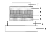
- the organic layer containing the compound of the present invention is preferably at least one layer selected from the group consisting of a light-emitting layer, an electron transport layer, a hole transport layer, an electron blocking layer and a hole blocking layer, and contains a phosphorescent dopant. More preferred is a light emitting layer.
- the structure of the organic EL element of the present invention will be described with reference to FIG. 1, but the structure of the organic EL element of the present invention is not limited to the illustrated one.
- FIG. 1 is a cross-sectional view showing a structural example of a general organic EL device used in the present invention, wherein 1 is a substrate, 2 is an anode, 3 is a hole injection layer, 4 is a hole transport layer, and 5 is a light emitting layer. , 6 represents an electron transport layer, and 7 represents a cathode.
- the organic EL device of the present invention may have an exciton blocking layer adjacent to the light emitting layer, and may have an electron blocking layer between the light emitting layer and the hole injection layer.
- the exciton blocking layer can be inserted on either the anode side or the cathode side of the light emitting layer, or both can be inserted simultaneously.
- the organic EL device of the present invention has a substrate, an anode, a light emitting layer and a cathode as essential layers, but it is preferable to have a hole injecting and transporting layer and an electron injecting and transporting layer in layers other than the essential layers, and further emitting It is preferable to have a hole blocking layer between the layer and the electron injecting and transporting layer.
- the hole injection / transport layer means either or both of a hole injection layer and a hole transport layer
- the electron injection / transport layer means either or both of an electron injection layer and an electron transport layer.
- the compound of the present invention or the material for an organic EL device can be used for any layer in the organic EL device. It is preferably used in a light emitting layer, a hole transport layer, an electron blocking layer, a hole blocking layer and an electron transport layer, and particularly preferably used as a light emitting layer, an electron transport layer and a hole blocking layer.
- the organic EL element of the present invention is preferably supported on a substrate.
- the substrate is not particularly limited as long as it is conventionally used for an organic EL element.
- a substrate made of glass, transparent plastic, quartz, or the like can be used.
- an electrode material made of a metal, an alloy, an electrically conductive compound, or a mixture thereof having a high work function (4 eV or more) is preferably used.
- electrode materials include metals such as Au, and conductive transparent materials such as CuI, indium tin oxide (ITO), SnO 2 and ZnO.
- conductive transparent materials such as CuI, indium tin oxide (ITO), SnO 2 and ZnO.
- an amorphous material such as IDIXO (In 2 O 3 —ZnO) that can form a transparent conductive film may be used.
- these electrode materials may be formed into a thin film by a method such as vapor deposition or sputtering, and a pattern having a desired shape may be formed by a photolithography method, or when the pattern accuracy is not required (about 100 ⁇ m or more) ), A pattern may be formed through a mask having a desired shape when the electrode material is deposited or sputtered. Or when using the substance which can be apply
- the cathode a material having a low work function (4 eV or less) metal (referred to as an electron injecting metal), an alloy, an electrically conductive compound, and a mixture thereof as an electrode material is used.
- an electron injecting metal a material having a low work function (4 eV or less) metal
- an alloy a material having a low work function (4 eV or less) metal
- an alloy a material having a low work function (4 eV or less) metal
- an alloy referred to as an electron injecting metal
- an alloy referred to as an electron injecting metal
- a mixture of an electron injecting metal and a second metal which is a stable metal having a larger work function than this for example, a magnesium / silver mixture
- Suitable are a magnesium / aluminum mixture, a magnesium / indium mixture, an aluminum / aluminum oxide (Al 2 O 3 ) mixture, a lithium / aluminum mixture, aluminum and the like.
- the cathode can be produced by forming a thin film of these electrode materials by a method such as vapor deposition or sputtering.
- the sheet resistance as the cathode is preferably several hundred ⁇ / ⁇ or less, and the film thickness is usually selected in the range of 10 nm to 5 ⁇ m, preferably 50 to 200 nm.
- the light emission luminance is improved, which is convenient.
- a transparent or semi-transparent cathode can be produced by producing the conductive transparent material mentioned in the description of the anode on the cathode after producing the metal with a thickness of 1 to 20 nm on the cathode.
- an element in which both the anode and the cathode are transmissive can be manufactured.
- the light emitting layer may be either a fluorescent light emitting layer or a phosphorescent light emitting layer, but is preferably a phosphorescent light emitting layer.
- the fluorescent light emitting material may be at least one kind of fluorescent light emitting material, but it is preferable to use the fluorescent light emitting material as a fluorescent light emitting dopant and include a host material. .
- the compound of the present invention can be used as the fluorescent light emitting material in the light emitting layer.
- the compound when the compound is used in any other organic layer, it is known from many patent documents and the like. You can also choose.
- Preferred examples include condensed aromatic compounds, styryl compounds, diketopyrrolopyrrole compounds, oxazine compounds, pyromethene metal complexes, transition metal complexes, and lanthanoid complexes. More preferred are naphthacene, pyrene, chrysene, triphenylene, benzo [c] phenanthrene.
- the amount of the fluorescent light emitting dopant contained in the light emitting layer is 0.01 to 20% by weight, preferably 0.1 to 10% by weight. It should be in range.
- an organic EL element injects electric charges into a luminescent material from both an anode and a cathode, generates an excited luminescent material, and emits light.
- a charge injection type organic EL element it is said that 25% of the generated excitons are excited to the excited singlet state and the remaining 75% are excited to the excited triplet state.
- a specific fluorescent substance is excited by triplet-triplet annihilation or absorption of thermal energy after energy transition to an excited triplet state due to intersystem crossing or the like. It is known that a singlet state is crossed between inverse systems to emit fluorescence and to express thermally activated delayed fluorescence.
- An organic EL device using the compound of the present invention can also exhibit delayed fluorescence. In this case, both fluorescence emission and delayed fluorescence emission can be included. However, light emission from the host material may be partly or partly emitted.
- the delayed fluorescent material can be used alone in the light emitting layer, but it is preferable to use the delayed fluorescent material as a delayed fluorescent light emitting dopant and mix the host material.
- the compound of the present invention can be used as the delayed fluorescent light emitting material in the light emitting layer, but it can also be selected from known delayed fluorescent light emitting materials. Examples include indolocarbazole derivatives described in non-patent literature Appl. Phys. Lett. 98, 083302 (2011) and carbazole derivatives described in Nature 492, 234 (2012). It is not limited.
- delayed fluorescent materials are shown below, but are not limited to the following compounds.
- the amount of the delayed fluorescent material contained in the light emitting layer is 0.01 to 50% by weight, preferably 0.1 to 20%. It is good to be in the range of wt%, more preferably 0.01 to 10%.
- the compound of the present invention can be used, but it can also be selected from compounds other than the compound of the present invention.
- a compound having a condensed aryl ring such as naphthalene, anthracene, phenanthrene, pyrene, chrysene, naphthacene, triphenylene, perylene, fluoranthene, fluorene, indene or a derivative thereof, N, N′-dinaphthyl-N, N′-diphenyl-4
- Aromatic amine derivatives such as 4,4'-diphenyl-1,1'-diamine
- metal chelated oxinoid compounds such as tris (8-quinolinato) aluminum (III)
- bisstyryl derivatives such as distyrylbenzene derivatives, tetraphenyl Butadiene derivatives, indene derivatives, coumarin derivatives, oxadiazole derivatives, pyrrolo
- Preferable phosphorescent dopants include complexes such as Ir (ppy) 3 having a noble metal element such as Ir as a central metal, complexes such as Ir (bt) 2 ⁇ acac3, and complexes such as PtOEt3. Specific examples of these complexes are shown below, but are not limited to the following compounds.
- the amount of the phosphorescent dopant contained in the light emitting layer is preferably in the range of 0.1 to 50% by weight. More preferably, it is 1 to 30% by weight.
- the compound of the present invention is preferably used as the host material in the emissive layer.
- the material used for the light emitting layer may be a host material other than the compound of the present invention.
- a plurality of known host materials may be used in combination.
- a known host compound that can be used is preferably a compound that has a hole transporting ability or an electron transporting ability, prevents the emission of light from becoming longer, and has a high glass transition temperature.
- Such other host materials are known from a large number of patent documents and can be selected from them.
- Specific examples of the host material are not particularly limited, but include indole derivatives, carbazole derivatives, indolocarbazole derivatives, triazole derivatives, oxazole derivatives, oxadiazole derivatives, imidazole derivatives, polyarylalkane derivatives, pyrazoline derivatives, Pyrazolone derivatives, phenylenediamine derivatives, arylamine derivatives, amino-substituted chalcone derivatives, styrylanthracene derivatives, fluorenone derivatives, hydrazone derivatives, stilbene derivatives, silazane derivatives, aromatic tertiary amine compounds, styrylamine compounds, aromatic dimethylidene compounds, porphyrins Compounds, anthraquinodimethane derivatives, anthrone derivatives, diphenylquinone derivatives, thiopyran dioxide derivative
- Tetracarboxylic anhydride Tetracarboxylic anhydride, phthalocyanine derivatives, metal complexes of 8-quinolinol derivatives, metal phthalocyanines, various metal complexes represented by metal complexes of benzoxazole and benzothiazole derivatives, polysilane compounds, poly (N-vinylcarbazole) derivatives, Examples include aniline-based copolymers, thiophene oligomers, polythiophene derivatives, polyphenylene derivatives, polyphenylene vinylene derivatives, and polyfluorene derivatives.
- the injection layer is a layer provided between the electrode and the organic layer for lowering the driving voltage and improving the luminance of light emission.
- the injection layer can be provided as necessary.
- the compound of the present invention can be used. However, when the compound is used in any other organic layer, any conventionally known compound can be selected and used. .
- the hole blocking layer has a function of an electron transport layer in a broad sense, and is made of a hole blocking material that has a function of transporting electrons and has a remarkably small ability to transport holes. The probability of recombination of electrons and holes can be improved by blocking.
- the compound of the present invention for the positive hole blocking layer, but when the compound is used for any other organic layer, a known hole blocking layer material may be used. Moreover, as a hole-blocking layer material, the material of the electron carrying layer mentioned later can be used as needed.
- the electron blocking layer is made of a material that has a function of transporting holes and has a very small ability to transport electrons.
- the electron blocking layer blocks the electrons while transporting holes, and the probability of recombination of electrons and holes. Can be improved.
- the compound of the present invention is preferably used. However, when the compound is used for any other organic layer, the material for the hole transport layer described later is used as necessary. Can do.
- the thickness of the electron blocking layer is preferably 3 to 100 nm, more preferably 5 to 30 nm.
- the exciton blocking layer is a layer for preventing excitons generated by recombination of holes and electrons in the light emitting layer from diffusing into the charge transport layer. It becomes possible to efficiently confine in the light emitting layer, and the light emission efficiency of the device can be improved.
- the exciton blocking layer can be inserted on either the anode side or the cathode side adjacent to the light emitting layer, or both can be inserted simultaneously.
- the compound of the present invention represented by the general formula (1) can be used as the material for the exciton blocking layer.
- a conventionally known compound is used. Any one can be selected and used. Examples thereof include mCP and bis (2-methyl-8-quinolinolato) -4-phenylphenolato aluminum (III) (BAlq).
- the hole transport layer is made of a hole transport material having a function of transporting holes, and the hole transport layer can be provided as a single layer or a plurality of layers.
- the hole transport material has either hole injection or transport or electron barrier properties, and may be either organic or inorganic. It is preferable to use the compound of the present invention for the hole transport layer. However, when the compound is used for any other organic layer, any one of conventionally known compounds may be selected and used. it can.
- Known hole transport materials that can be used include, for example, porphyrin compounds, aromatic tertiary amine compounds, styrylamine compounds, triazole derivatives, oxadiazole derivatives, imidazole derivatives, polyarylalkane derivatives, pyrazoline derivatives and pyrazolone derivatives, amino acids.
- Substituted chalcone derivatives, oxazole derivatives, styrylanthracene derivatives, fluorenone derivatives, hydrazone derivatives, stilbene derivatives, silazane derivatives, aniline-based copolymers, and conductive polymer oligomers, particularly thiophene oligomers, include porphyrin compounds, aromatics It is preferable to use a tertiary amine compound and a styrylamine compound, and it is more preferable to use an aromatic tertiary amine compound.
- the electron transport layer is made of a material having a function of transporting electrons, and the electron transport layer can be provided as a single layer or a plurality of layers.
- an electron transport material which may also serve as a hole blocking material
- the compound of the present invention is preferably used for the electron transport layer.
- any one of conventionally known compounds can be selected and used. Examples thereof include nitro-substituted fluorene derivatives, diphenylquinone derivatives, thiopyran dioxide derivatives, carbodiimides, fluorenylidenemethane derivatives, anthraquinodimethane and anthrone derivatives, oxadiazole derivatives, and the like.
- a thiadiazole derivative in which the oxygen atom of the oxadiazole ring is substituted with a sulfur atom, and a quinoxaline derivative having a quinoxaline ring known as an electron withdrawing group can also be used as an electron transport material.
- a polymer material in which these materials are introduced into a polymer chain or these materials are used as a polymer main chain can also be used.
- the compound of the present invention was synthesized by the route shown below.
- the compound number corresponds to the number assigned to the above chemical formula.
- intermediate (A-3) 50.0 g (0.11 mol), 2,3-dichloro-5,6-dicyano-1,4-benzoquinone 26.5 g (0.12 ⁇ ⁇ ⁇ ⁇ mol), toluene 500 ml, distilled water 50 ml And stirred at 80 ° C. for 14 hours. Then, the solvent was distilled off under reduced pressure, dissolved in ethyl acetate, the organic layer was washed with distilled water (2 ⁇ 100 ml), and then the obtained organic layer was dried over anhydrous magnesium sulfate. Left. The resulting residue was purified by column chromatography to obtain 17.7 g (0.051 mol, yield 48%) of intermediate (A-4).
- Example 7 Each thin film was laminated at a vacuum degree of 2.0 ⁇ 10 ⁇ 5 Pa by a vacuum deposition method on a glass substrate on which an anode made of indium tin oxide (ITO) having a thickness of 110 nm was formed.
- ITO indium tin oxide
- CuPC copper phthalocyanine
- N, N-di (naphthalen-1-yl) -N, N-diphenyl-benzidene (NPB) was formed to a thickness of 90 nm as a hole transport layer.
- the compound (1-25) as the host material of the light emitting layer and the iridium complex FIrpic as the blue phosphor material as the dopant were co-deposited on the hole transport layer from different deposition sources, and the thickness was 30 nm. Then, a light emitting layer was formed. The concentration of FIrpic was 10%.
- Alq3 was formed to a thickness of 30 nm as an electron transport layer. Further, on the electron transport layer, lithium fluoride (LiF) was formed to a thickness of 1.0 nm as an electron injection layer. Finally, aluminum (Al) was formed as an electrode to a thickness of 70 nm on the electron injection layer, and an organic EL element was produced.
- the organic EL element had the light emission characteristics as shown in Table 1.
- Table 1 the brightness, voltage, and luminous efficiency show values at 2.5 mA / cm 2 .
- the maximum wavelength of the device emission spectrum was 475 nm, indicating that light emission from FIrpic was obtained.
- Examples 8-12 As a host material of the light emitting layer of Example 7, instead of the compound (1-25), the compound (1-1), (3-2), (3-1), (1-2), or (3-10 ) was used to produce an organic EL device in the same manner as in Example 7. The maximum wavelength of the device emission spectrum was 475 nm, and it was identified that light emission from FIrpic was obtained.
- Comparative Example 1 An organic EL device was produced in the same manner as in Example 1 except that mCP was used as the host material for the light emitting layer. The maximum wavelength of the device emission spectrum was 475 nm, and it was identified that light emission from FIrpic was obtained.
- An organic EL device was produced in the same manner as in Example 1 except that the compound (C-4) was used as the host material for the emissive layer.
- the maximum wavelength of the device emission spectrum was 475 nm, and it was identified that light emission from FIrpic was obtained.
- Table 1 summarizes the measurement results of the host material used and the light emission characteristics (@ 2.5 mA / cm 2 ).
- Example 13 Each thin film was laminated at a vacuum degree of 4.0 ⁇ 10 ⁇ 5 Pa by a vacuum deposition method on a glass substrate on which an anode made of ITO having a thickness of 110 nm was formed.
- CuPC was formed to a thickness of 25 nm on ITO.
- NPB was formed to a thickness of 40 nm as a hole transport layer.
- the compound (1-25) as the host material and Ir (ppy) 3 as the phosphorescent dopant are co-evaporated from different vapor deposition sources to emit light with a thickness of 40 nm.
- a layer was formed.
- the concentration of Ir (ppy) 3 in the light emitting layer was 10.0 wt%.
- Alq3 was formed to a thickness of 20 nm as an electron transport layer. Further, LiF was formed on the electron transport layer to a thickness of 1.0 nm as an electron injection layer. Finally, on the electron injection layer, Al was formed to a thickness of 70 nm as an electrode to produce an organic EL device.
- the organic EL element had the light emission characteristics as shown in Table 2.
- the luminance, voltage, and luminous efficiency show values at 10 mA / cm 2 .
- the maximum wavelength of the device emission spectrum was 530 nm, and it was found that light was emitted from Ir (ppy) 3 .
- Examples 14-18 As the host material of the light emitting layer of Example 13, the compound (1-1), (3-2), (3-1), (1-2), or (3-10) was used instead of the compound (1-25) ) was used to produce an organic EL device in the same manner as in Example 13.
- the maximum wavelength of the emission spectrum of each device was 530 nm, and it was found that light emission from Ir (ppy) 3 was obtained.
- Comparative Examples 3-4 An organic EL device was produced in the same manner as in Example 13 except that CBP and (C-4) were used as the host material of the light emitting layer in Example 5. The maximum wavelength of the device emission spectrum was 535 nm, and it was identified that light emission from Ir (ppy) 3 was obtained.
- Table 2 summarizes the measurement results of the host material used and the light emission characteristics (@ 10 mA / cm 2 ).
Abstract
Priority Applications (5)
| Application Number | Priority Date | Filing Date | Title |
|---|---|---|---|
| US14/404,255 US9761811B2 (en) | 2012-06-28 | 2013-05-15 | Organic electroluminescence element and material for organic electroluminescence element |
| JP2014522475A JP6153522B2 (ja) | 2012-06-28 | 2013-05-15 | 有機電界発光素子用材料及び有機電界発光素子 |
| KR1020157002214A KR102014888B1 (ko) | 2012-06-28 | 2013-05-15 | 유기 전계발광 소자용 재료 및 유기 전계발광 소자 |
| CN201380034130.0A CN104396042B (zh) | 2012-06-28 | 2013-05-15 | 有机电致发光元件用材料及有机电致发光元件 |
| EP13808847.1A EP2869356B1 (fr) | 2012-06-28 | 2013-05-15 | Élément à électroluminescence organique et matériau pour un élément à électroluminescence organique |
Applications Claiming Priority (2)
| Application Number | Priority Date | Filing Date | Title |
|---|---|---|---|
| JP2012145210 | 2012-06-28 | ||
| JP2012-145210 | 2012-06-28 |
Publications (1)
| Publication Number | Publication Date |
|---|---|
| WO2014002629A1 true WO2014002629A1 (fr) | 2014-01-03 |
Family
ID=49782801
Family Applications (1)
| Application Number | Title | Priority Date | Filing Date |
|---|---|---|---|
| PCT/JP2013/063497 WO2014002629A1 (fr) | 2012-06-28 | 2013-05-15 | Élément à électroluminescence organique et matériau pour un élément à électroluminescence organique |
Country Status (7)
| Country | Link |
|---|---|
| US (1) | US9761811B2 (fr) |
| EP (1) | EP2869356B1 (fr) |
| JP (1) | JP6153522B2 (fr) |
| KR (1) | KR102014888B1 (fr) |
| CN (1) | CN104396042B (fr) |
| TW (1) | TWI567164B (fr) |
| WO (1) | WO2014002629A1 (fr) |
Cited By (7)
| Publication number | Priority date | Publication date | Assignee | Title |
|---|---|---|---|---|
| WO2016107446A1 (fr) * | 2014-12-31 | 2016-07-07 | 北京维信诺科技有限公司 | Dispositif électroluminescent organique |
| WO2016119533A1 (fr) * | 2015-01-26 | 2016-08-04 | 北京维信诺科技有限公司 | Dispositif électroluminescent organique phosphorescent sensibilisé thermiquement activé |
| WO2016181844A1 (fr) * | 2015-05-08 | 2016-11-17 | コニカミノルタ株式会社 | Composé pi-conjugué, corps fluorescent retardé, film mince électroluminescent, élément électroluminescent organique, dispositif d'affichage et dispositif d'éclairage |
| JP2017137258A (ja) * | 2016-02-03 | 2017-08-10 | コニカミノルタ株式会社 | π共役系化合物の製造方法 |
| US10522760B2 (en) | 2016-10-04 | 2019-12-31 | Samsung Display Co., Ltd. | Polycyclic compound and organic electroluminescence device including the same |
| WO2020050162A1 (fr) * | 2018-09-03 | 2020-03-12 | 国立大学法人大阪大学 | Matériau el organique et dispositif el organique |
| US10787467B2 (en) | 2016-11-30 | 2020-09-29 | Samsung Display Co., Ltd. | Polycyclic compound and organic electroluminescence device including the same |
Families Citing this family (11)
| Publication number | Priority date | Publication date | Assignee | Title |
|---|---|---|---|---|
| KR102034341B1 (ko) * | 2013-08-01 | 2019-10-18 | 고쿠리쓰다이가쿠호진 규슈다이가쿠 | 화합물, 발광 재료 및 유기 발광 소자 |
| US20160284913A1 (en) * | 2015-03-27 | 2016-09-29 | Staffan WESTERBERG | Solar cell emitter region fabrication using substrate-level ion implantation |
| CN106800570B (zh) * | 2016-12-15 | 2018-11-27 | 南京邮电大学 | 基于硅嗪单元的光电功能材料及其制备方法和应用 |
| US10538538B2 (en) | 2017-01-13 | 2020-01-21 | Samsung Display Co., Ltd. | Polycyclic compound and organic electroluminescence device including the same |
| KR20180085860A (ko) * | 2017-01-19 | 2018-07-30 | 삼성디스플레이 주식회사 | 유기 전계 발광 소자 |
| CN107325037B (zh) * | 2017-05-24 | 2020-03-13 | 北京八亿时空液晶科技股份有限公司 | 一种1-溴咔唑的制备方法 |
| CN108424420B (zh) * | 2017-09-30 | 2021-01-12 | 北京绿人科技有限责任公司 | 含有硅原子的三嗪化合物及其应用和一种有机电致发光器件 |
| CN111971289B (zh) * | 2018-04-25 | 2023-12-08 | 株式会社Lg化学 | 化合物和包含其的有机发光器件 |
| CN108912157A (zh) * | 2018-10-08 | 2018-11-30 | 天津理工大学 | 一种简单高效合成硼氮杂芳烃的方法 |
| CN109796451B (zh) * | 2019-02-18 | 2020-07-14 | 中国科学院化学研究所 | 一种以萘啶作为电子受体的多色热激活延迟荧光材料及其制备方法与应用 |
| CN113603715A (zh) * | 2021-08-23 | 2021-11-05 | 黑龙江省科学院石油化学研究院 | 一种10,10-二苯基硅杂吖啶的制备方法 |
Citations (98)
| Publication number | Priority date | Publication date | Assignee | Title |
|---|---|---|---|---|
| JPH08302339A (ja) | 1995-05-02 | 1996-11-19 | Toppan Printing Co Ltd | 有機薄膜el素子 |
| WO2001041512A1 (fr) | 1999-12-01 | 2001-06-07 | The Trustees Of Princeton University | Complexes de forme l2mx en tant que dopants phosphorescents pour del organiques |
| JP2001313178A (ja) | 2000-04-28 | 2001-11-09 | Pioneer Electronic Corp | 有機エレクトロルミネッセンス素子 |
| JP2002117978A (ja) | 2000-07-17 | 2002-04-19 | Fuji Photo Film Co Ltd | 発光素子及びイリジウム錯体 |
| JP2003073387A (ja) | 2001-09-04 | 2003-03-12 | Canon Inc | 金属配位化合物及び有機発光素子 |
| JP2003123982A (ja) | 2001-08-07 | 2003-04-25 | Fuji Photo Film Co Ltd | 発光素子及び新規イリジウム錯体 |
| JP2003133074A (ja) | 2001-02-01 | 2003-05-09 | Fuji Photo Film Co Ltd | 遷移金属錯体及び発光素子 |
| JP2003253128A (ja) | 2002-02-28 | 2003-09-10 | Jsr Corp | 発光性組成物 |
| JP2003253145A (ja) | 2002-02-28 | 2003-09-10 | Jsr Corp | 発光性組成物 |
| JP2003253129A (ja) | 2002-02-28 | 2003-09-10 | Jsr Corp | 発光性組成物 |
| JP2003272861A (ja) | 2002-03-12 | 2003-09-26 | Konica Corp | 有機エレクトロルミネッセンス素子及びそれを用いた表示装置 |
| JP2004059433A (ja) | 2001-06-15 | 2004-02-26 | Sanyo Electric Co Ltd | 発光性有機金属化合物及び発光素子 |
| JP2004506305A (ja) | 2000-08-11 | 2004-02-26 | ザ、トラスティーズ オブ プリンストン ユニバーシティ | 有機金属化合物及び放射移行有機電気燐光体 |
| JP2004111193A (ja) | 2002-09-18 | 2004-04-08 | Konica Minolta Holdings Inc | 有機エレクトロルミネッセンス素子及び表示装置 |
| WO2004045001A2 (fr) | 2002-11-08 | 2004-05-27 | Universal Display Corporation | Matériaux et dispositifs électroluminescents organiques |
| WO2004045000A2 (fr) | 2002-11-06 | 2004-05-27 | Universal Display Corporation | Matieres et dispositifs electroluminescents organiques |
| JP2004155709A (ja) | 2002-11-06 | 2004-06-03 | Toyota Central Res & Dev Lab Inc | 有機金属錯体化合物及びこれを用いた有機発光素子 |
| JP2004319438A (ja) | 2003-03-28 | 2004-11-11 | Konica Minolta Holdings Inc | 有機エレクトロルミネッセンス素子、表示装置、照明装置及びロジウム錯体化合物 |
| JP2005038847A (ja) | 2003-06-26 | 2005-02-10 | Samsung Sdi Co Ltd | 有機金属錯体およびこれを採用した有機電界発光素子 |
| JP2005082598A (ja) | 2003-09-06 | 2005-03-31 | Samsung Sdi Co Ltd | 二核有機金属錯体及びそれを利用した有機電界発光素子 |
| US20050119485A1 (en) | 2002-11-06 | 2005-06-02 | Brown Cory S. | Organometallic compounds for use in electroluminescent devices |
| JP2005139185A (ja) | 2003-11-06 | 2005-06-02 | Samsung Sdi Co Ltd | 有機金属錯体及びこれを用いた有機電界発光素子 |
| JP2005187473A (ja) | 2003-12-24 | 2005-07-14 | Samsung Sdi Co Ltd | ニ核有機金属錯体及びこれを利用した有機電界発光素子 |
| JP2005220136A (ja) | 2004-02-02 | 2005-08-18 | Samsung Sdi Co Ltd | イリジウム化合物及びそれを利用した有機電界発光素子 |
| WO2005076380A2 (fr) | 2004-02-03 | 2005-08-18 | Universal Display Corporation | Dispositifs oled utilisant des systemes de ligand multidente |
| US20050214576A1 (en) | 2000-08-11 | 2005-09-29 | Sergey Lamansky | Organometallic compounds and emission-shifting organic electrophosphorescence |
| US20050260448A1 (en) | 2004-05-18 | 2005-11-24 | Chun Lin | Novel organometallic compounds for use in electroluminescent devices |
| US20050260449A1 (en) | 2004-05-18 | 2005-11-24 | Robert Walters | Complexes with tridentate ligands |
| WO2005113704A2 (fr) | 2004-05-18 | 2005-12-01 | The University Of Southern California | Composes luminescents a ligands carbene |
| JP2006050596A (ja) | 2004-07-06 | 2006-02-16 | Canon Inc | データ処理方法、データ処理装置、ディザパターン製造方法およびディザパターン |
| JP2006063080A (ja) | 2004-08-28 | 2006-03-09 | Samsung Sdi Co Ltd | シクロメタル化遷移金属錯体及びこれを利用した有機電界発光素子 |
| JP2006093542A (ja) | 2004-09-27 | 2006-04-06 | Fuji Photo Film Co Ltd | 発光素子 |
| JP2006513278A (ja) | 2002-08-16 | 2006-04-20 | ザ ユニバーシティ オブ サザン カリフォルニア | 有機発光材料及びデバイス |
| WO2006041263A1 (fr) | 2004-10-13 | 2006-04-20 | Doosan Corporation | Composes chromophores et dispositif d'affichage electroluminescent organique comprenant ces composes |
| JP2006104201A (ja) | 2004-10-01 | 2006-04-20 | Samsung Sdi Co Ltd | シクロメタル化遷移金属錯体及びこれを用いた有機電界発光素子 |
| JP2006104132A (ja) | 2004-10-06 | 2006-04-20 | Toppan Printing Co Ltd | 有機金属錯体、および発光材料、並びに発光素子 |
| JP2006111623A (ja) | 2004-10-11 | 2006-04-27 | Samsung Sdi Co Ltd | シクロメタル化遷移金属錯体及びこれを用いた有機電界発光素子 |
| WO2006046980A1 (fr) | 2004-07-06 | 2006-05-04 | Universal Display Corporation | Matériaux et dispositifs électroluminescents organiques |
| JP2006131561A (ja) | 2004-11-08 | 2006-05-25 | Idemitsu Kosan Co Ltd | 金属錯体化合物 |
| JP2006131524A (ja) | 2004-11-04 | 2006-05-25 | Fuji Photo Film Co Ltd | 有機金属錯体、発光性固体、有機el素子及び有機elディスプレイ |
| JP2006213720A (ja) | 2005-02-03 | 2006-08-17 | Samsung Sdi Co Ltd | 有機金属錯体及びこれを用いた有機電界発光素子 |
| WO2006100888A1 (fr) | 2005-03-22 | 2006-09-28 | Konica Minolta Holdings, Inc. | Materiau pour dispositif el organique, dispositif el organique, dispositif d’affichage et d’eclairage |
| JP2006261623A (ja) | 2004-09-22 | 2006-09-28 | Fuji Photo Film Co Ltd | 有機電界発光素子 |
| JP2006290891A (ja) | 2005-04-12 | 2006-10-26 | Samsung Sdi Co Ltd | シリル置換シクロメタル化遷移金属錯体およびこれを用いた有機電界発光素子 |
| JP2006298900A (ja) | 2005-04-21 | 2006-11-02 | Samsung Sdi Co Ltd | ホスト用化合物とドーパント用化合物が連結された有機金属化合物、およびこれを利用した有機電界発光素子及びその製造方法 |
| JP2006303383A (ja) | 2005-04-25 | 2006-11-02 | Fuji Photo Film Co Ltd | 有機電界発光素子 |
| JP2006303394A (ja) | 2005-04-25 | 2006-11-02 | Fuji Photo Film Co Ltd | 有機電界発光素子 |
| JP2006298899A (ja) | 2005-04-21 | 2006-11-02 | Samsung Sdi Co Ltd | ホスト用化合物とドーパント用化合物が連結された有機金属化合物、およびこれを利用した有機電界発光素子及びその製造方法 |
| JP2006310479A (ja) | 2005-04-27 | 2006-11-09 | Fuji Photo Film Co Ltd | 有機電界発光素子 |
| WO2007004380A1 (fr) | 2005-07-01 | 2007-01-11 | Konica Minolta Holdings, Inc. | Matériau pour élément électroluminescent organique, élément électroluminescent organique, dispositif d’affichage et équipement d’éclairage |
| JP2007002080A (ja) | 2005-06-23 | 2007-01-11 | Konica Minolta Holdings Inc | 有機エレクトロルミネッセンス素子材料、有機エレクトロルミネッセンス素子、表示装置及び照明装置 |
| JP2007009009A (ja) | 2005-06-29 | 2007-01-18 | Konica Minolta Holdings Inc | 有機エレクトロルミネッセンス素子材料、有機エレクトロルミネッセンス素子、表示装置及び照明装置 |
| WO2007018067A1 (fr) | 2005-08-05 | 2007-02-15 | Idemitsu Kosan Co., Ltd. | Composé complexe de métaux de transition et dispositif électroluminescent organique l’utilisant |
| WO2007023659A1 (fr) | 2005-08-25 | 2007-03-01 | Konica Minolta Holdings, Inc. | Matériau pour dispositif électroluminescent organique, dispositif électroluminescent organique, dispositif d’affichage, et dispositif d'éclairage |
| JP2007088105A (ja) | 2005-09-20 | 2007-04-05 | Fujifilm Corp | 有機電界発光素子 |
| WO2007058080A1 (fr) | 2005-11-17 | 2007-05-24 | Idemitsu Kosan Co., Ltd. | Compose forme d'un complexe metallique et element electroluminescent organique contenant ledit compose |
| WO2007058104A1 (fr) | 2005-11-17 | 2007-05-24 | Idemitsu Kosan Co., Ltd. | Composes formes d'un complexe metallique et dispositifs electroluminescents organiques obtenus a l'aide desdits composes |
| JP2007522126A (ja) | 2004-01-26 | 2007-08-09 | ユニバーサル ディスプレイ コーポレーション | 改善された電界発光安定性 |
| WO2007095118A2 (fr) | 2006-02-10 | 2007-08-23 | Universal Display Corporation | COMPLEXES MÉTALLIQUES DE IMIDAZO[1,2-f]PHÉNANTHRIDINE CYCLOMÉTALLÉE ET DE LIGANDS DIIMIDAZO[1,2-A:1',2'-C]QUINAZOLINE ET LEURS ANALOGUES ISOÉLECTRONIQUES ET BENZANNELÉS |
| JP2007227948A (ja) | 2007-03-29 | 2007-09-06 | Konica Minolta Holdings Inc | 有機エレクトロルミネッセンス素子及びそれを用いた表示装置 |
| JP2007258550A (ja) | 2006-03-24 | 2007-10-04 | Fujifilm Corp | 有機電界発光素子 |
| JP2007324309A (ja) | 2006-05-31 | 2007-12-13 | Fujifilm Corp | 有機電界発光素子 |
| JP2008037848A (ja) | 2006-08-10 | 2008-02-21 | Takasago Internatl Corp | 白金錯体及び発光素子 |
| JP2008505925A (ja) | 2004-07-07 | 2008-02-28 | ユニバーサル ディスプレイ コーポレイション | 安定で効率的なエレクトロルミネセンス材料 |
| WO2008035664A1 (fr) | 2006-09-20 | 2008-03-27 | Konica Minolta Holdings, Inc. | Matériau de dispositif électroluminescent organique, dispositif électroluminescent organique, dispositif d'affichage et d'éclairage |
| JP2008091906A (ja) | 2007-09-26 | 2008-04-17 | Konica Minolta Holdings Inc | 有機エレクトロルミネッセンス素子 |
| WO2008050733A1 (fr) | 2006-10-24 | 2008-05-02 | Ube Industries, Ltd. | Complexe de l'or, procédé pour la production du complexe de l'or et élément électroluminescent ultraviolet organique utilisant le complexe de l'or |
| WO2008054584A1 (fr) | 2006-11-03 | 2008-05-08 | Universal Display Corporation | Matériaux de dispositif organique émetteur de lumière (oled) à stabilité améliorée, et dispositifs |
| JP2008133212A (ja) | 2006-11-28 | 2008-06-12 | Canon Inc | 金属錯体化合物、電界発光素子及び表示装置 |
| JP2008239565A (ja) | 2007-03-28 | 2008-10-09 | Idemitsu Kosan Co Ltd | イリジウム錯体とその製造法及びそれを用いた有機エレクトロルミネッセンス |
| US20080261076A1 (en) | 2007-03-08 | 2008-10-23 | Universal Display Corporation | Phosphorescent materials |
| JP2008270737A (ja) | 2007-03-23 | 2008-11-06 | Fujifilm Corp | 有機電界発光素子 |
| JP2008266163A (ja) | 2007-04-17 | 2008-11-06 | Idemitsu Kosan Co Ltd | 遷移金属錯体化合物及びそれを用いた有機エレクトロルミネッセンス素子 |
| WO2008140657A1 (fr) | 2007-05-10 | 2008-11-20 | Universal Display Corporation | Composés organométalliques ayant des fonctionnalités d'hôte et de dopant |
| JP2008542203A (ja) | 2005-05-06 | 2008-11-27 | ユニバーサル ディスプレイ コーポレイション | 安定oled材料及び改善された安定性を有するデバイス |
| WO2008156879A1 (fr) | 2007-06-20 | 2008-12-24 | Universal Display Corporation | Matériaux à base d'imidazophénantridine phosphorescente bleue |
| JP2008311607A (ja) | 2007-05-16 | 2008-12-25 | Konica Minolta Holdings Inc | 有機エレクトロルミネッセンス素子、有機エレクトロルミネッセンス素子材料、表示装置及び照明装置 |
| JP2009019121A (ja) | 2007-07-12 | 2009-01-29 | Konica Minolta Holdings Inc | 有機エレクトロルミネッセンス材料、有機エレクトロルミネッセンス素子、表示装置及び照明装置 |
| JP2009046601A (ja) | 2007-08-21 | 2009-03-05 | Konica Minolta Holdings Inc | 有機エレクトロルミネッセンス素子材料、有機エレクトロルミネッセンス素子、表示装置及び照明装置 |
| JP2009057367A (ja) | 2007-08-03 | 2009-03-19 | Idemitsu Kosan Co Ltd | 金属錯体化合物、有機エレクトロルミネッセンス素子用材料及びそれを用いた有機エレクトロルミネッセンス素子 |
| JP2009057304A (ja) | 2007-08-30 | 2009-03-19 | Mitsubishi Chemicals Corp | 金属錯体及び有機電界発光素子 |
| WO2009046266A1 (fr) | 2007-10-04 | 2009-04-09 | Universal Display Corporation | Complexes incorporant des ligands tridentates |
| JP2009096800A (ja) | 2007-09-25 | 2009-05-07 | Fujifilm Corp | 有機電界発光素子 |
| JP2009114369A (ja) | 2007-11-08 | 2009-05-28 | Konica Minolta Holdings Inc | 有機エレクトロルミネッセンス材料、有機エレクトロルミネッセンス素子、表示装置及び照明装置 |
| WO2009073245A1 (fr) | 2007-12-06 | 2009-06-11 | Universal Display Corporation | Complexes organométalliques électroluminescents |
| JP2009161524A (ja) | 2007-12-14 | 2009-07-23 | Fujifilm Corp | 白金錯体化合物及びこれを用いた有機電界発光素子 |
| JP2009532546A (ja) | 2006-04-07 | 2009-09-10 | ソルヴェイ(ソシエテ アノニム) | 発光物質 |
| JP2009536681A (ja) | 2006-05-08 | 2009-10-15 | イー・アイ・デュポン・ドウ・ヌムール・アンド・カンパニー | エレクトロルミネセンスビス−シクロメタレート化イリジウム化合物およびかかる化合物で作製されたデバイス |
| JP2009542026A (ja) | 2006-06-26 | 2009-11-26 | ビーエーエスエフ ソシエタス・ヨーロピア | 架橋カルベン配位子を有するPtとPdのビスカルベン錯体及びテトラカルベン錯体のOLED内での利用 |
| JP2009286716A (ja) | 2008-05-28 | 2009-12-10 | Sumitomo Seika Chem Co Ltd | イリジウム錯体 |
| JP2009292807A (ja) * | 2008-04-23 | 2009-12-17 | Gracel Display Inc | 新規の有機電界発光化合物およびこれを使用する有機電界発光素子 |
| JP2010059158A (ja) * | 2008-09-04 | 2010-03-18 | Gracel Display Inc | 新規な有機電界発光化合物およびこれを用いる有機電界発光素子 |
| JP2010059144A (ja) * | 2008-06-25 | 2010-03-18 | Gracel Display Inc | 新規な有機電界発光化合物及びこれを使用する有機電界発光素子 |
| JP2010083852A (ja) | 2008-10-03 | 2010-04-15 | Wakayama Univ | 金属錯体の製造方法、金属錯体および有機電界発光素子 |
| WO2011136484A1 (fr) * | 2010-04-30 | 2011-11-03 | Rohm And Haas Electronic Materials Korea Ltd. | Nouveaux composés organiques électroluminescents et dispositif organique électroluminescent associé |
| JP2011228615A (ja) * | 2010-03-31 | 2011-11-10 | Fujifilm Corp | 光電変換素子及びその製造方法、光センサ、並びに撮像素子及びそれらの駆動方法 |
| WO2012007103A1 (fr) * | 2010-07-15 | 2012-01-19 | Merck Patent Gmbh | Complexes métalliques comportant des ligands organiques et leur utilisation dans des oled |
| WO2013024693A1 (fr) * | 2011-08-16 | 2013-02-21 | 富士フイルム株式会社 | Élément de conversion photoélectrique ainsi que procédé de mise en œuvre de celui-ci, élément de capture d'images, et capteur optique |
Family Cites Families (6)
| Publication number | Priority date | Publication date | Assignee | Title |
|---|---|---|---|---|
| JP2004200141A (ja) * | 2002-10-24 | 2004-07-15 | Toyota Industries Corp | 有機el素子 |
| CN1895004A (zh) * | 2003-12-15 | 2007-01-10 | 出光兴产株式会社 | 有机电致发光元件用材料及使用其的有机电致发光元件 |
| US7820844B2 (en) * | 2007-10-22 | 2010-10-26 | Chien-Hong Cheng | Conjugated compounds containing heteroatom-center-arylsilane derivatives and their application |
| WO2010140645A1 (fr) * | 2009-06-03 | 2010-12-09 | 富士フイルム株式会社 | Élément de conversion photoélectrique et son procédé de production, photocapteur, élément d'imagerie et son procédé de pilotage |
| KR20110119206A (ko) * | 2010-04-27 | 2011-11-02 | 다우어드밴스드디스플레이머티리얼 유한회사 | 신규한 유기 발광 화합물 및 이를 포함하는 유기 발광 소자 |
| US8927749B2 (en) * | 2013-03-07 | 2015-01-06 | Universal Display Corporation | Organic electroluminescent materials and devices |
-
2013
- 2013-05-15 EP EP13808847.1A patent/EP2869356B1/fr active Active
- 2013-05-15 JP JP2014522475A patent/JP6153522B2/ja active Active
- 2013-05-15 KR KR1020157002214A patent/KR102014888B1/ko active IP Right Grant
- 2013-05-15 US US14/404,255 patent/US9761811B2/en active Active
- 2013-05-15 WO PCT/JP2013/063497 patent/WO2014002629A1/fr active Application Filing
- 2013-05-15 CN CN201380034130.0A patent/CN104396042B/zh active Active
- 2013-05-30 TW TW102119173A patent/TWI567164B/zh not_active IP Right Cessation
Patent Citations (98)
| Publication number | Priority date | Publication date | Assignee | Title |
|---|---|---|---|---|
| JPH08302339A (ja) | 1995-05-02 | 1996-11-19 | Toppan Printing Co Ltd | 有機薄膜el素子 |
| WO2001041512A1 (fr) | 1999-12-01 | 2001-06-07 | The Trustees Of Princeton University | Complexes de forme l2mx en tant que dopants phosphorescents pour del organiques |
| JP2001313178A (ja) | 2000-04-28 | 2001-11-09 | Pioneer Electronic Corp | 有機エレクトロルミネッセンス素子 |
| JP2002117978A (ja) | 2000-07-17 | 2002-04-19 | Fuji Photo Film Co Ltd | 発光素子及びイリジウム錯体 |
| JP2004506305A (ja) | 2000-08-11 | 2004-02-26 | ザ、トラスティーズ オブ プリンストン ユニバーシティ | 有機金属化合物及び放射移行有機電気燐光体 |
| US20050214576A1 (en) | 2000-08-11 | 2005-09-29 | Sergey Lamansky | Organometallic compounds and emission-shifting organic electrophosphorescence |
| JP2003133074A (ja) | 2001-02-01 | 2003-05-09 | Fuji Photo Film Co Ltd | 遷移金属錯体及び発光素子 |
| JP2004059433A (ja) | 2001-06-15 | 2004-02-26 | Sanyo Electric Co Ltd | 発光性有機金属化合物及び発光素子 |
| JP2003123982A (ja) | 2001-08-07 | 2003-04-25 | Fuji Photo Film Co Ltd | 発光素子及び新規イリジウム錯体 |
| JP2003073387A (ja) | 2001-09-04 | 2003-03-12 | Canon Inc | 金属配位化合物及び有機発光素子 |
| JP2003253145A (ja) | 2002-02-28 | 2003-09-10 | Jsr Corp | 発光性組成物 |
| JP2003253129A (ja) | 2002-02-28 | 2003-09-10 | Jsr Corp | 発光性組成物 |
| JP2003253128A (ja) | 2002-02-28 | 2003-09-10 | Jsr Corp | 発光性組成物 |
| JP2003272861A (ja) | 2002-03-12 | 2003-09-26 | Konica Corp | 有機エレクトロルミネッセンス素子及びそれを用いた表示装置 |
| JP2006513278A (ja) | 2002-08-16 | 2006-04-20 | ザ ユニバーシティ オブ サザン カリフォルニア | 有機発光材料及びデバイス |
| JP2004111193A (ja) | 2002-09-18 | 2004-04-08 | Konica Minolta Holdings Inc | 有機エレクトロルミネッセンス素子及び表示装置 |
| WO2004045000A2 (fr) | 2002-11-06 | 2004-05-27 | Universal Display Corporation | Matieres et dispositifs electroluminescents organiques |
| US20050119485A1 (en) | 2002-11-06 | 2005-06-02 | Brown Cory S. | Organometallic compounds for use in electroluminescent devices |
| JP2004155709A (ja) | 2002-11-06 | 2004-06-03 | Toyota Central Res & Dev Lab Inc | 有機金属錯体化合物及びこれを用いた有機発光素子 |
| WO2004045001A2 (fr) | 2002-11-08 | 2004-05-27 | Universal Display Corporation | Matériaux et dispositifs électroluminescents organiques |
| JP2004319438A (ja) | 2003-03-28 | 2004-11-11 | Konica Minolta Holdings Inc | 有機エレクトロルミネッセンス素子、表示装置、照明装置及びロジウム錯体化合物 |
| JP2005038847A (ja) | 2003-06-26 | 2005-02-10 | Samsung Sdi Co Ltd | 有機金属錯体およびこれを採用した有機電界発光素子 |
| JP2005082598A (ja) | 2003-09-06 | 2005-03-31 | Samsung Sdi Co Ltd | 二核有機金属錯体及びそれを利用した有機電界発光素子 |
| JP2005139185A (ja) | 2003-11-06 | 2005-06-02 | Samsung Sdi Co Ltd | 有機金属錯体及びこれを用いた有機電界発光素子 |
| JP2005187473A (ja) | 2003-12-24 | 2005-07-14 | Samsung Sdi Co Ltd | ニ核有機金属錯体及びこれを利用した有機電界発光素子 |
| JP2007522126A (ja) | 2004-01-26 | 2007-08-09 | ユニバーサル ディスプレイ コーポレーション | 改善された電界発光安定性 |
| JP2005220136A (ja) | 2004-02-02 | 2005-08-18 | Samsung Sdi Co Ltd | イリジウム化合物及びそれを利用した有機電界発光素子 |
| WO2005076380A2 (fr) | 2004-02-03 | 2005-08-18 | Universal Display Corporation | Dispositifs oled utilisant des systemes de ligand multidente |
| US20050260448A1 (en) | 2004-05-18 | 2005-11-24 | Chun Lin | Novel organometallic compounds for use in electroluminescent devices |
| WO2005113704A2 (fr) | 2004-05-18 | 2005-12-01 | The University Of Southern California | Composes luminescents a ligands carbene |
| US20050260449A1 (en) | 2004-05-18 | 2005-11-24 | Robert Walters | Complexes with tridentate ligands |
| WO2006046980A1 (fr) | 2004-07-06 | 2006-05-04 | Universal Display Corporation | Matériaux et dispositifs électroluminescents organiques |
| JP2006050596A (ja) | 2004-07-06 | 2006-02-16 | Canon Inc | データ処理方法、データ処理装置、ディザパターン製造方法およびディザパターン |
| JP2008505925A (ja) | 2004-07-07 | 2008-02-28 | ユニバーサル ディスプレイ コーポレイション | 安定で効率的なエレクトロルミネセンス材料 |
| JP2006063080A (ja) | 2004-08-28 | 2006-03-09 | Samsung Sdi Co Ltd | シクロメタル化遷移金属錯体及びこれを利用した有機電界発光素子 |
| JP2006261623A (ja) | 2004-09-22 | 2006-09-28 | Fuji Photo Film Co Ltd | 有機電界発光素子 |
| JP2006093542A (ja) | 2004-09-27 | 2006-04-06 | Fuji Photo Film Co Ltd | 発光素子 |
| JP2006104201A (ja) | 2004-10-01 | 2006-04-20 | Samsung Sdi Co Ltd | シクロメタル化遷移金属錯体及びこれを用いた有機電界発光素子 |
| JP2006104132A (ja) | 2004-10-06 | 2006-04-20 | Toppan Printing Co Ltd | 有機金属錯体、および発光材料、並びに発光素子 |
| JP2006111623A (ja) | 2004-10-11 | 2006-04-27 | Samsung Sdi Co Ltd | シクロメタル化遷移金属錯体及びこれを用いた有機電界発光素子 |
| WO2006041263A1 (fr) | 2004-10-13 | 2006-04-20 | Doosan Corporation | Composes chromophores et dispositif d'affichage electroluminescent organique comprenant ces composes |
| JP2006131524A (ja) | 2004-11-04 | 2006-05-25 | Fuji Photo Film Co Ltd | 有機金属錯体、発光性固体、有機el素子及び有機elディスプレイ |
| JP2006131561A (ja) | 2004-11-08 | 2006-05-25 | Idemitsu Kosan Co Ltd | 金属錯体化合物 |
| JP2006213720A (ja) | 2005-02-03 | 2006-08-17 | Samsung Sdi Co Ltd | 有機金属錯体及びこれを用いた有機電界発光素子 |
| WO2006100888A1 (fr) | 2005-03-22 | 2006-09-28 | Konica Minolta Holdings, Inc. | Materiau pour dispositif el organique, dispositif el organique, dispositif d’affichage et d’eclairage |
| JP2006290891A (ja) | 2005-04-12 | 2006-10-26 | Samsung Sdi Co Ltd | シリル置換シクロメタル化遷移金属錯体およびこれを用いた有機電界発光素子 |
| JP2006298900A (ja) | 2005-04-21 | 2006-11-02 | Samsung Sdi Co Ltd | ホスト用化合物とドーパント用化合物が連結された有機金属化合物、およびこれを利用した有機電界発光素子及びその製造方法 |
| JP2006298899A (ja) | 2005-04-21 | 2006-11-02 | Samsung Sdi Co Ltd | ホスト用化合物とドーパント用化合物が連結された有機金属化合物、およびこれを利用した有機電界発光素子及びその製造方法 |
| JP2006303383A (ja) | 2005-04-25 | 2006-11-02 | Fuji Photo Film Co Ltd | 有機電界発光素子 |
| JP2006303394A (ja) | 2005-04-25 | 2006-11-02 | Fuji Photo Film Co Ltd | 有機電界発光素子 |
| JP2006310479A (ja) | 2005-04-27 | 2006-11-09 | Fuji Photo Film Co Ltd | 有機電界発光素子 |
| JP2008542203A (ja) | 2005-05-06 | 2008-11-27 | ユニバーサル ディスプレイ コーポレイション | 安定oled材料及び改善された安定性を有するデバイス |
| JP2007002080A (ja) | 2005-06-23 | 2007-01-11 | Konica Minolta Holdings Inc | 有機エレクトロルミネッセンス素子材料、有機エレクトロルミネッセンス素子、表示装置及び照明装置 |
| JP2007009009A (ja) | 2005-06-29 | 2007-01-18 | Konica Minolta Holdings Inc | 有機エレクトロルミネッセンス素子材料、有機エレクトロルミネッセンス素子、表示装置及び照明装置 |
| WO2007004380A1 (fr) | 2005-07-01 | 2007-01-11 | Konica Minolta Holdings, Inc. | Matériau pour élément électroluminescent organique, élément électroluminescent organique, dispositif d’affichage et équipement d’éclairage |
| WO2007018067A1 (fr) | 2005-08-05 | 2007-02-15 | Idemitsu Kosan Co., Ltd. | Composé complexe de métaux de transition et dispositif électroluminescent organique l’utilisant |
| WO2007023659A1 (fr) | 2005-08-25 | 2007-03-01 | Konica Minolta Holdings, Inc. | Matériau pour dispositif électroluminescent organique, dispositif électroluminescent organique, dispositif d’affichage, et dispositif d'éclairage |
| JP2007088105A (ja) | 2005-09-20 | 2007-04-05 | Fujifilm Corp | 有機電界発光素子 |
| WO2007058080A1 (fr) | 2005-11-17 | 2007-05-24 | Idemitsu Kosan Co., Ltd. | Compose forme d'un complexe metallique et element electroluminescent organique contenant ledit compose |
| WO2007058104A1 (fr) | 2005-11-17 | 2007-05-24 | Idemitsu Kosan Co., Ltd. | Composes formes d'un complexe metallique et dispositifs electroluminescents organiques obtenus a l'aide desdits composes |
| WO2007095118A2 (fr) | 2006-02-10 | 2007-08-23 | Universal Display Corporation | COMPLEXES MÉTALLIQUES DE IMIDAZO[1,2-f]PHÉNANTHRIDINE CYCLOMÉTALLÉE ET DE LIGANDS DIIMIDAZO[1,2-A:1',2'-C]QUINAZOLINE ET LEURS ANALOGUES ISOÉLECTRONIQUES ET BENZANNELÉS |
| JP2007258550A (ja) | 2006-03-24 | 2007-10-04 | Fujifilm Corp | 有機電界発光素子 |
| JP2009532546A (ja) | 2006-04-07 | 2009-09-10 | ソルヴェイ(ソシエテ アノニム) | 発光物質 |
| JP2009536681A (ja) | 2006-05-08 | 2009-10-15 | イー・アイ・デュポン・ドウ・ヌムール・アンド・カンパニー | エレクトロルミネセンスビス−シクロメタレート化イリジウム化合物およびかかる化合物で作製されたデバイス |
| JP2007324309A (ja) | 2006-05-31 | 2007-12-13 | Fujifilm Corp | 有機電界発光素子 |
| JP2009542026A (ja) | 2006-06-26 | 2009-11-26 | ビーエーエスエフ ソシエタス・ヨーロピア | 架橋カルベン配位子を有するPtとPdのビスカルベン錯体及びテトラカルベン錯体のOLED内での利用 |
| JP2008037848A (ja) | 2006-08-10 | 2008-02-21 | Takasago Internatl Corp | 白金錯体及び発光素子 |
| WO2008035664A1 (fr) | 2006-09-20 | 2008-03-27 | Konica Minolta Holdings, Inc. | Matériau de dispositif électroluminescent organique, dispositif électroluminescent organique, dispositif d'affichage et d'éclairage |
| WO2008050733A1 (fr) | 2006-10-24 | 2008-05-02 | Ube Industries, Ltd. | Complexe de l'or, procédé pour la production du complexe de l'or et élément électroluminescent ultraviolet organique utilisant le complexe de l'or |
| WO2008054584A1 (fr) | 2006-11-03 | 2008-05-08 | Universal Display Corporation | Matériaux de dispositif organique émetteur de lumière (oled) à stabilité améliorée, et dispositifs |
| JP2008133212A (ja) | 2006-11-28 | 2008-06-12 | Canon Inc | 金属錯体化合物、電界発光素子及び表示装置 |
| US20080261076A1 (en) | 2007-03-08 | 2008-10-23 | Universal Display Corporation | Phosphorescent materials |
| JP2008270737A (ja) | 2007-03-23 | 2008-11-06 | Fujifilm Corp | 有機電界発光素子 |
| JP2008239565A (ja) | 2007-03-28 | 2008-10-09 | Idemitsu Kosan Co Ltd | イリジウム錯体とその製造法及びそれを用いた有機エレクトロルミネッセンス |
| JP2007227948A (ja) | 2007-03-29 | 2007-09-06 | Konica Minolta Holdings Inc | 有機エレクトロルミネッセンス素子及びそれを用いた表示装置 |
| JP2008266163A (ja) | 2007-04-17 | 2008-11-06 | Idemitsu Kosan Co Ltd | 遷移金属錯体化合物及びそれを用いた有機エレクトロルミネッセンス素子 |
| WO2008140657A1 (fr) | 2007-05-10 | 2008-11-20 | Universal Display Corporation | Composés organométalliques ayant des fonctionnalités d'hôte et de dopant |
| JP2008311607A (ja) | 2007-05-16 | 2008-12-25 | Konica Minolta Holdings Inc | 有機エレクトロルミネッセンス素子、有機エレクトロルミネッセンス素子材料、表示装置及び照明装置 |
| WO2008156879A1 (fr) | 2007-06-20 | 2008-12-24 | Universal Display Corporation | Matériaux à base d'imidazophénantridine phosphorescente bleue |
| JP2009019121A (ja) | 2007-07-12 | 2009-01-29 | Konica Minolta Holdings Inc | 有機エレクトロルミネッセンス材料、有機エレクトロルミネッセンス素子、表示装置及び照明装置 |
| JP2009057367A (ja) | 2007-08-03 | 2009-03-19 | Idemitsu Kosan Co Ltd | 金属錯体化合物、有機エレクトロルミネッセンス素子用材料及びそれを用いた有機エレクトロルミネッセンス素子 |
| JP2009046601A (ja) | 2007-08-21 | 2009-03-05 | Konica Minolta Holdings Inc | 有機エレクトロルミネッセンス素子材料、有機エレクトロルミネッセンス素子、表示装置及び照明装置 |
| JP2009057304A (ja) | 2007-08-30 | 2009-03-19 | Mitsubishi Chemicals Corp | 金属錯体及び有機電界発光素子 |
| JP2009096800A (ja) | 2007-09-25 | 2009-05-07 | Fujifilm Corp | 有機電界発光素子 |
| JP2008091906A (ja) | 2007-09-26 | 2008-04-17 | Konica Minolta Holdings Inc | 有機エレクトロルミネッセンス素子 |
| WO2009046266A1 (fr) | 2007-10-04 | 2009-04-09 | Universal Display Corporation | Complexes incorporant des ligands tridentates |
| JP2009114369A (ja) | 2007-11-08 | 2009-05-28 | Konica Minolta Holdings Inc | 有機エレクトロルミネッセンス材料、有機エレクトロルミネッセンス素子、表示装置及び照明装置 |
| WO2009073245A1 (fr) | 2007-12-06 | 2009-06-11 | Universal Display Corporation | Complexes organométalliques électroluminescents |
| JP2009161524A (ja) | 2007-12-14 | 2009-07-23 | Fujifilm Corp | 白金錯体化合物及びこれを用いた有機電界発光素子 |
| JP2009292807A (ja) * | 2008-04-23 | 2009-12-17 | Gracel Display Inc | 新規の有機電界発光化合物およびこれを使用する有機電界発光素子 |
| JP2009286716A (ja) | 2008-05-28 | 2009-12-10 | Sumitomo Seika Chem Co Ltd | イリジウム錯体 |
| JP2010059144A (ja) * | 2008-06-25 | 2010-03-18 | Gracel Display Inc | 新規な有機電界発光化合物及びこれを使用する有機電界発光素子 |
| JP2010059158A (ja) * | 2008-09-04 | 2010-03-18 | Gracel Display Inc | 新規な有機電界発光化合物およびこれを用いる有機電界発光素子 |
| JP2010083852A (ja) | 2008-10-03 | 2010-04-15 | Wakayama Univ | 金属錯体の製造方法、金属錯体および有機電界発光素子 |
| JP2011228615A (ja) * | 2010-03-31 | 2011-11-10 | Fujifilm Corp | 光電変換素子及びその製造方法、光センサ、並びに撮像素子及びそれらの駆動方法 |
| WO2011136484A1 (fr) * | 2010-04-30 | 2011-11-03 | Rohm And Haas Electronic Materials Korea Ltd. | Nouveaux composés organiques électroluminescents et dispositif organique électroluminescent associé |
| WO2012007103A1 (fr) * | 2010-07-15 | 2012-01-19 | Merck Patent Gmbh | Complexes métalliques comportant des ligands organiques et leur utilisation dans des oled |
| WO2013024693A1 (fr) * | 2011-08-16 | 2013-02-21 | 富士フイルム株式会社 | Élément de conversion photoélectrique ainsi que procédé de mise en œuvre de celui-ci, élément de capture d'images, et capteur optique |
Non-Patent Citations (5)
| Title |
|---|
| APPL. PHYS. LETT., vol. 98, 2011, pages 083302 |
| APPLIED PHYSICS LETTERS, vol. 82, 2003, pages 2422 - 2424 |
| APPLIED PHYSICS LETTERS, vol. 83, 2003, pages 569 - 571 |
| NATURE, vol. 492, 2012, pages 234 |
| See also references of EP2869356A4 |
Cited By (14)
| Publication number | Priority date | Publication date | Assignee | Title |
|---|---|---|---|---|
| US10566542B2 (en) | 2014-12-31 | 2020-02-18 | Beijing Visionox Technology Co., Ltd. | Organic electroluminescent device |
| CN105810846A (zh) * | 2014-12-31 | 2016-07-27 | 北京维信诺科技有限公司 | 一种有机电致发光器件 |
| WO2016107446A1 (fr) * | 2014-12-31 | 2016-07-07 | 北京维信诺科技有限公司 | Dispositif électroluminescent organique |
| CN105810846B (zh) * | 2014-12-31 | 2020-07-07 | 北京维信诺科技有限公司 | 一种有机电致发光器件 |
| KR20170093906A (ko) * | 2014-12-31 | 2017-08-16 | 베이징 비젼녹스 테크놀로지 컴퍼니 리미티드 | 유기전계발광소자 |
| EP3226320A4 (fr) * | 2014-12-31 | 2017-12-20 | Beijing Visionox Technology Co., Ltd. | Dispositif électroluminescent organique |
| JP2018501660A (ja) * | 2014-12-31 | 2018-01-18 | 北京維信諾科技有限公司 | 有機エレクトロルミネッセンス素子 |
| KR102013506B1 (ko) * | 2014-12-31 | 2019-08-22 | 베이징 비젼녹스 테크놀로지 컴퍼니 리미티드 | 유기전계발광소자 |
| WO2016119533A1 (fr) * | 2015-01-26 | 2016-08-04 | 北京维信诺科技有限公司 | Dispositif électroluminescent organique phosphorescent sensibilisé thermiquement activé |
| WO2016181844A1 (fr) * | 2015-05-08 | 2016-11-17 | コニカミノルタ株式会社 | Composé pi-conjugué, corps fluorescent retardé, film mince électroluminescent, élément électroluminescent organique, dispositif d'affichage et dispositif d'éclairage |
| JP2017137258A (ja) * | 2016-02-03 | 2017-08-10 | コニカミノルタ株式会社 | π共役系化合物の製造方法 |
| US10522760B2 (en) | 2016-10-04 | 2019-12-31 | Samsung Display Co., Ltd. | Polycyclic compound and organic electroluminescence device including the same |
| US10787467B2 (en) | 2016-11-30 | 2020-09-29 | Samsung Display Co., Ltd. | Polycyclic compound and organic electroluminescence device including the same |
| WO2020050162A1 (fr) * | 2018-09-03 | 2020-03-12 | 国立大学法人大阪大学 | Matériau el organique et dispositif el organique |
Also Published As
| Publication number | Publication date |
|---|---|
| KR20150033700A (ko) | 2015-04-01 |
| JP6153522B2 (ja) | 2017-06-28 |
| US20150188056A1 (en) | 2015-07-02 |
| TWI567164B (zh) | 2017-01-21 |
| EP2869356A4 (fr) | 2016-02-17 |
| US9761811B2 (en) | 2017-09-12 |
| EP2869356A1 (fr) | 2015-05-06 |
| CN104396042A (zh) | 2015-03-04 |
| JPWO2014002629A1 (ja) | 2016-05-30 |
| KR102014888B1 (ko) | 2019-08-27 |
| CN104396042B (zh) | 2016-10-12 |
| TW201410842A (zh) | 2014-03-16 |
| EP2869356B1 (fr) | 2016-10-12 |
Similar Documents
| Publication | Publication Date | Title |
|---|---|---|
| JP6153522B2 (ja) | 有機電界発光素子用材料及び有機電界発光素子 | |
| KR102133241B1 (ko) | 유기 전계 발광 소자용 아다만탄 화합물 및 유기 전계 발광 소자 | |
| KR102097718B1 (ko) | 유기 전계발광 소자용 화합물 및 유기 전계발광 소자 | |
| JP5399418B2 (ja) | 有機電界発光素子 | |
| WO2013088934A1 (fr) | Matériau d'élément électroluminescent organique et élément électroluminescent organique qui utilise ce dernier | |
| KR20130009765A (ko) | 유기 전계 발광 소자 | |
| KR102135228B1 (ko) | 유기 전계발광 소자용 붕소 화합물 및 유기 전계발광 소자 | |
| JP5778756B2 (ja) | 含窒素芳香族化合物及び有機電界発光素子 | |
| JP6647283B2 (ja) | 有機電界発光素子用材料及びこれを用いた有機電界発光素子 | |
| JP6169078B2 (ja) | 有機電界発光素子 | |
| KR20150100890A (ko) | 유기전계발광 소자용 재료 및 이것을 사용한 유기전계발광 소자 | |
| EP3125325B1 (fr) | Matériau d'élément électroluminescent organique et élément électroluminescent organique l'utilisant | |
| JP6402177B2 (ja) | 有機電界発光素子用材料及びこれを用いた有機電界発光素子 | |
| WO2013038929A1 (fr) | Matériau pour élément électroluminescent organique ayant une structure de cycle à quatre chaînons contenant du silicium, et élément électroluminescent organique l'utilisant | |
| JP2018170369A (ja) | 有機電界発光素子用材料及びこれを用いた有機電界発光素子 | |
| JP6846258B2 (ja) | 有機電界発光素子用材料及びこれを用いた有機電界発光素子 |
Legal Events
| Date | Code | Title | Description |
|---|---|---|---|
| 121 | Ep: the epo has been informed by wipo that ep was designated in this application |
Ref document number: 13808847 Country of ref document: EP Kind code of ref document: A1 |
|
| ENP | Entry into the national phase |
Ref document number: 2014522475 Country of ref document: JP Kind code of ref document: A |
|
| WWE | Wipo information: entry into national phase |
Ref document number: 14404255 Country of ref document: US |
|
| REEP | Request for entry into the european phase |
Ref document number: 2013808847 Country of ref document: EP |
|
| WWE | Wipo information: entry into national phase |
Ref document number: 2013808847 Country of ref document: EP |
|
| NENP | Non-entry into the national phase |
Ref country code: DE |
|
| ENP | Entry into the national phase |
Ref document number: 20157002214 Country of ref document: KR Kind code of ref document: A |