WO2012124362A1 - 樹脂多層基板 - Google Patents
樹脂多層基板 Download PDFInfo
- Publication number
- WO2012124362A1 WO2012124362A1 PCT/JP2012/050672 JP2012050672W WO2012124362A1 WO 2012124362 A1 WO2012124362 A1 WO 2012124362A1 JP 2012050672 W JP2012050672 W JP 2012050672W WO 2012124362 A1 WO2012124362 A1 WO 2012124362A1
- Authority
- WO
- WIPO (PCT)
- Prior art keywords
- surface electrode
- conductor pattern
- plane conductor
- resin multilayer
- substrate body
- Prior art date
Links
Images


Classifications
-
- H—ELECTRICITY
- H05—ELECTRIC TECHNIQUES NOT OTHERWISE PROVIDED FOR
- H05K—PRINTED CIRCUITS; CASINGS OR CONSTRUCTIONAL DETAILS OF ELECTRIC APPARATUS; MANUFACTURE OF ASSEMBLAGES OF ELECTRICAL COMPONENTS
- H05K1/00—Printed circuits
- H05K1/02—Details
- H05K1/11—Printed elements for providing electric connections to or between printed circuits
- H05K1/115—Via connections; Lands around holes or via connections
- H05K1/116—Lands, clearance holes or other lay-out details concerning the surrounding of a via
-
- H—ELECTRICITY
- H05—ELECTRIC TECHNIQUES NOT OTHERWISE PROVIDED FOR
- H05K—PRINTED CIRCUITS; CASINGS OR CONSTRUCTIONAL DETAILS OF ELECTRIC APPARATUS; MANUFACTURE OF ASSEMBLAGES OF ELECTRICAL COMPONENTS
- H05K3/00—Apparatus or processes for manufacturing printed circuits
- H05K3/46—Manufacturing multilayer circuits
- H05K3/4611—Manufacturing multilayer circuits by laminating two or more circuit boards
- H05K3/4626—Manufacturing multilayer circuits by laminating two or more circuit boards characterised by the insulating layers or materials
- H05K3/4632—Manufacturing multilayer circuits by laminating two or more circuit boards characterised by the insulating layers or materials laminating thermoplastic or uncured resin sheets comprising printed circuits without added adhesive materials between the sheets
-
- H—ELECTRICITY
- H05—ELECTRIC TECHNIQUES NOT OTHERWISE PROVIDED FOR
- H05K—PRINTED CIRCUITS; CASINGS OR CONSTRUCTIONAL DETAILS OF ELECTRIC APPARATUS; MANUFACTURE OF ASSEMBLAGES OF ELECTRICAL COMPONENTS
- H05K2201/00—Indexing scheme relating to printed circuits covered by H05K1/00
- H05K2201/01—Dielectrics
- H05K2201/0104—Properties and characteristics in general
- H05K2201/0129—Thermoplastic polymer, e.g. auto-adhesive layer; Shaping of thermoplastic polymer
-
- H—ELECTRICITY
- H05—ELECTRIC TECHNIQUES NOT OTHERWISE PROVIDED FOR
- H05K—PRINTED CIRCUITS; CASINGS OR CONSTRUCTIONAL DETAILS OF ELECTRIC APPARATUS; MANUFACTURE OF ASSEMBLAGES OF ELECTRICAL COMPONENTS
- H05K2201/00—Indexing scheme relating to printed circuits covered by H05K1/00
- H05K2201/09—Shape and layout
- H05K2201/09209—Shape and layout details of conductors
- H05K2201/09372—Pads and lands
- H05K2201/09427—Special relation between the location or dimension of a pad or land and the location or dimension of a terminal
-
- H—ELECTRICITY
- H05—ELECTRIC TECHNIQUES NOT OTHERWISE PROVIDED FOR
- H05K—PRINTED CIRCUITS; CASINGS OR CONSTRUCTIONAL DETAILS OF ELECTRIC APPARATUS; MANUFACTURE OF ASSEMBLAGES OF ELECTRICAL COMPONENTS
- H05K2201/00—Indexing scheme relating to printed circuits covered by H05K1/00
- H05K2201/09—Shape and layout
- H05K2201/09209—Shape and layout details of conductors
- H05K2201/09372—Pads and lands
- H05K2201/09481—Via in pad; Pad over filled via
-
- H—ELECTRICITY
- H05—ELECTRIC TECHNIQUES NOT OTHERWISE PROVIDED FOR
- H05K—PRINTED CIRCUITS; CASINGS OR CONSTRUCTIONAL DETAILS OF ELECTRIC APPARATUS; MANUFACTURE OF ASSEMBLAGES OF ELECTRICAL COMPONENTS
- H05K2201/00—Indexing scheme relating to printed circuits covered by H05K1/00
- H05K2201/09—Shape and layout
- H05K2201/09209—Shape and layout details of conductors
- H05K2201/095—Conductive through-holes or vias
- H05K2201/09509—Blind vias, i.e. vias having one side closed
- H05K2201/09527—Inverse blind vias, i.e. bottoms outwards in multilayer PCB; Blind vias in centre of PCB having opposed bottoms
-
- H—ELECTRICITY
- H05—ELECTRIC TECHNIQUES NOT OTHERWISE PROVIDED FOR
- H05K—PRINTED CIRCUITS; CASINGS OR CONSTRUCTIONAL DETAILS OF ELECTRIC APPARATUS; MANUFACTURE OF ASSEMBLAGES OF ELECTRICAL COMPONENTS
- H05K2201/00—Indexing scheme relating to printed circuits covered by H05K1/00
- H05K2201/09—Shape and layout
- H05K2201/09209—Shape and layout details of conductors
- H05K2201/095—Conductive through-holes or vias
- H05K2201/096—Vertically aligned vias, holes or stacked vias
-
- H—ELECTRICITY
- H05—ELECTRIC TECHNIQUES NOT OTHERWISE PROVIDED FOR
- H05K—PRINTED CIRCUITS; CASINGS OR CONSTRUCTIONAL DETAILS OF ELECTRIC APPARATUS; MANUFACTURE OF ASSEMBLAGES OF ELECTRICAL COMPONENTS
- H05K2201/00—Indexing scheme relating to printed circuits covered by H05K1/00
- H05K2201/09—Shape and layout
- H05K2201/09209—Shape and layout details of conductors
- H05K2201/09654—Shape and layout details of conductors covering at least two types of conductors provided for in H05K2201/09218 - H05K2201/095
- H05K2201/09781—Dummy conductors, i.e. not used for normal transport of current; Dummy electrodes of components
-
- H—ELECTRICITY
- H05—ELECTRIC TECHNIQUES NOT OTHERWISE PROVIDED FOR
- H05K—PRINTED CIRCUITS; CASINGS OR CONSTRUCTIONAL DETAILS OF ELECTRIC APPARATUS; MANUFACTURE OF ASSEMBLAGES OF ELECTRICAL COMPONENTS
- H05K3/00—Apparatus or processes for manufacturing printed circuits
- H05K3/46—Manufacturing multilayer circuits
- H05K3/4611—Manufacturing multilayer circuits by laminating two or more circuit boards
- H05K3/4614—Manufacturing multilayer circuits by laminating two or more circuit boards the electrical connections between the circuit boards being made during lamination
- H05K3/4617—Manufacturing multilayer circuits by laminating two or more circuit boards the electrical connections between the circuit boards being made during lamination characterized by laminating only or mainly similar single-sided circuit boards
Definitions
- the present invention relates to a resin multilayer substrate, and more particularly to a resin multilayer substrate including a substrate body on which an insulating layer made of a resin material is laminated.
- 121b are laminated and pressure-bonded while being heated to produce the resin multilayer substrate 100.
- the interlayer connection conductor 151 is connected to the surface electrode formed by the conductor pattern 122 exposed on the mounting surface 160 of the substrate body 139 in which the pattern films 121, 121 a, 121 b are integrated by heat fusion.
- the resin multilayer substrate Since the resin multilayer substrate has flexibility, it can be used as a flexible substrate. However, when the resin multilayer substrate is bent and used, the surface electrode is easily peeled off from the substrate body.
- the present invention intends to provide a resin multilayer substrate capable of suppressing the peeling of the surface electrode from the substrate body.
- the present invention provides a resin multilayer substrate configured as follows.
- the resin multilayer substrate includes: (a) a substrate body on which an insulating layer made of a resin material is laminated; (b) a surface electrode formed on one main surface of the substrate body; and (c) the insulating layers adjacent to each other. And an in-plane conductor pattern facing the surface electrode.
- the in-plane conductor pattern overlaps with the surface electrode and protrudes outside the surface electrode with an interval over the entire circumference of the surface electrode when seen through from the stacking direction in which the insulating layers are stacked.
- the surface electrode faces the in-plane conductor pattern larger than the surface electrode
- the surface electrode and the surface electrode The resin material of the insulating layer sandwiched between the in-plane conductive patterns facing the electrodes has no escape in the stacking direction. Therefore, the pressure acting on the interface between the surface electrode and the insulating layer is increased. Thereby, the bonding between the surface electrode and the insulating layer can be strengthened, and peeling of the surface electrode from the substrate body can be suppressed.
- an interlayer connection conductor that penetrates the insulating layer and connects the surface electrode and the in-plane conductor pattern is provided.
- the portion where the surface electrode and the in-plane conductor pattern are connected via the interlayer connection conductor is formed of a conductive metal or the like, and is less likely to deform than the resin material of the insulating layer. Therefore, when bending deformation occurs in the substrate body, the deformation of the insulating layer around the surface electrode is constrained, and the substrate body is less deformed in the vicinity of the surface electrode. Thereby, peeling of the surface electrode from the substrate body can be suppressed.
- a slit is formed in the in-plane conductor pattern.
- the insulating layers arranged on both sides of the in-plane conductor pattern in which the slit is formed are joined to each other through the slit formed in the in-plane conductor pattern.
- a through hole is formed in the in-plane conductor pattern.
- the insulating layers arranged on both sides of the in-plane conductor pattern in which the through hole is formed are joined to each other through the through hole formed in the in-plane conductor pattern.
- only the insulating layer or only the interlayer connection conductor and the insulating layer are disposed between the surface electrode and the in-plane conductor pattern.
- the distance between the surface electrode and the in-plane conductor pattern can be shortened to further suppress deformation in the vicinity of the surface electrode and further suppress peeling of the surface electrode from the substrate body.
- a back electrode formed on the other main surface of the substrate body is further provided opposite to the front electrode.
- the interlayer connection conductor is connected to the back electrode.
- the portion where the front surface electrode, the back surface electrode, and the interlayer connection conductor are connected is formed of a conductive metal or the like and is less likely to be deformed than the insulating layer of the resin material.
- peeling of the surface electrode from the substrate body can be suppressed.
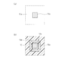
- Example 1 It is sectional drawing of a resin multilayer substrate.
- Example 1 It is principal part sectional drawing of a resin multilayer substrate.
- Example 1 It is sectional drawing which shows the manufacturing process of a resin multilayer substrate.
- Example 1 It is sectional drawing which shows the manufacturing process of a resin multilayer substrate.
- Example 1 It is sectional drawing of a resin multilayer substrate.
- Example 2 It is principal part sectional drawing of a resin multilayer substrate.
- Example 2 It is principal part sectional drawing of a resin multilayer substrate.
- (Modification) It is sectional drawing which shows the manufacturing process of a resin multilayer substrate. (Conventional example)
- Example 1 The resin multilayer substrate 10 of Example 1 will be described with reference to FIGS.
- FIG. 1 is a cross-sectional view of the resin multilayer substrate 10.
- FIG. 2A is a cross-sectional view of the principal part taken along line AA in FIG.
- FIG. 2B is a cross-sectional view of the main part taken along line BB in FIG.
- the resin multilayer substrate 10 has a surface electrode 18 a formed on one main surface 12 a of a substrate body 12 on which an insulating layer made of a resin material is laminated, and the other main surface of the substrate body 12.
- a back electrode 18b is formed on the surface 12b.
- one of the front electrode 18a and the back electrode 18b is used as an external electrode for mounting the resin multilayer substrate 10 on another circuit board or the like, and the other is for mounting an electronic component on the resin multilayer substrate 10. Used as a land electrode.
- in-plane conductor patterns 14, 14a, 14b disposed between adjacent insulating layers of the substrate body 12 and an interlayer connection conductor 16 penetrating the insulating layer are formed.
- the in-plane conductor pattern 14a facing the surface electrode 18a overlaps with the surface electrode 18a and is spaced over the entire circumference of the surface electrode 18a when viewed from the stacking direction in which the insulating layers are stacked. And protrudes outside the surface electrode 18a.
- the in-plane conductor pattern 14a is larger than the surface electrode 18a.
- the surface electrode 18a is opposed to the in-plane conductor pattern 14a larger than the surface electrode 18a, when the insulating layer made of the resin material is pressure-bonded in the step of manufacturing the resin multilayer substrate 10, the surface electrode The resin material of the insulating layer sandwiched between 18a and the in-plane conductor pattern 14a facing the surface electrode 18a has no escape in the stacking direction. Therefore, the pressure acting on the interface between the surface electrode 18a and the insulating layer is increased. Thereby, the bonding between the surface electrode 18a and the insulating layer can be strengthened, and the peeling of the surface electrode 18a from the substrate body 12 can be suppressed.
- the portion where the surface electrode 18a and the in-plane conductor pattern 14a are connected via the interlayer connection conductor 16 is formed of a conductive metal or the like, and is less likely to be deformed than the resin material of the insulating layer. For this reason, when bending deformation occurs in the substrate body 12, the deformation of the insulating layer around the surface electrode 18a is constrained, and the substrate body 12 is less deformed in the vicinity of the surface electrode 18a. Thereby, peeling of the surface electrode 18a from the substrate body 12 can be suppressed.
- the in-plane conductor pattern 14b facing the back electrode 18b overlaps with the back electrode 18b when seen through from the stacking direction in which the insulating layers are stacked, and the back electrode 18b. Are spaced outside the back electrode 18b with a space around the entire circumference.
- the in-plane conductor pattern 14b is larger than the back electrode 18b.
- the interlayer connection conductor 16 is connected to the front surface electrode 18a, the in-plane conductor patterns 14, 14a, 14b, and the back surface electrode 18b, penetrates the substrate body 12, and is formed in a column shape.
- the portion where the interlayer connection conductor 16 is connected to the front surface electrode 18a and the back surface electrode 18b is formed of a conductive metal or the like and is less likely to be deformed than an insulating layer of a resin material. To do. Thereby, since the deformation
- FIGS. 3 and 4 are cross-sectional views showing the manufacturing steps of the resin multilayer substrate 10.
- a resin sheet 11 for forming the substrate body 12 is prepared.
- LCP liquid crystal polymer
- PPS polyphenylene
- a metal foil 13 such as Cu, Ag, Sn, Ni, Au or an alloy thereof is attached to one main surface 11t.
- a resin sheet 11 made of a thermoplastic resin material such as sulfide), PEEK (polyetheretherketone), or PI (polyimide) is prepared.
- the other main surface 11s side of the resin sheet 11 is prepared.
- a through hole (via hole) 11p reaching the metal foil 13 is formed by a method such as laser processing.
- the mask pattern 2 is formed on the metal foil 13 so as to cover the position corresponding to the through hole 11p, for example, by applying a photoresist, exposing, and developing. After etching the metal foil 13 as shown in FIG. 3D, the mask pattern 2 is removed as shown in FIG. As a result, portions that become the in-plane conductor patterns 14, 14a, 14b are formed.
- the via-hole conductor 15 is formed by filling the through hole 11p with a conductive paste by a method such as screen printing.
- the resin sheets 11a to 11f that become the insulating layers of the substrate body 12 are laminated in a predetermined direction to form a laminate 11x.
- the laminated body 11x is pressure-bonded while heating to form the substrate body 12.
- the via-hole conductor 15 is cured and the interlayer connection conductor 16 is formed.
- the resin multilayer substrate 10 can be manufactured.
- Example 2 The resin multilayer substrate 10a of Example 2 will be described with reference to FIGS.
- FIG. 5 is a cross-sectional view of the resin multilayer substrate 10a.
- FIG. 6A is a cross-sectional view of the principal part taken along line AA in FIG.
- FIG. 6B is a cross-sectional view of the principal part taken along line BB in FIG.
- the resin multilayer substrate 10a of Example 2 is configured in substantially the same manner as the resin multilayer substrate 10 of Example 1.
- the same reference numerals are used for the same components as in the first embodiment, and differences from the first embodiment will be mainly described.
- the in-plane conductor pattern 14s facing the surface electrode 18a overlaps with the surface electrode 18a when seen through from the stacking direction in which the insulating layers are stacked, as in the first embodiment.
- the electrode 18a protrudes outward from the surface electrode 18a with an interval around the entire circumference.
- the in-plane conductor pattern 14s is larger than the surface electrode 18a.
- a slit 14m is formed in the in-plane conductor pattern 14s facing the surface electrode 18a.
- the slit 14m is formed so as to communicate with the corner of the in-plane conductor pattern 14s and surround the outer surface of the surface electrode 18a when seen through from the stacking direction in which the insulating layers are stacked.
- the slit 14m can be formed so as to partially overlap the surface electrode 18a when seen through from the stacking direction. However, if the slit 14m is formed so as not to overlap the surface electrode 18a, the slit 14m It is preferable because the pressure is difficult to escape from the slit 14m, the pressure acting between the surface electrode 18a and the insulating layer can be increased, and the bonding between the surface electrode 18a and the insulating layer can be strengthened.
- the insulating layers arranged on both sides of the in-plane conductor pattern 14s where the slit 14m is formed and sandwiching the in-plane conductor pattern 14s are joined via the slit 14m of the in-plane conductor pattern 14s.
- the in-plane conductor pattern 14t facing the back electrode 18b is configured in the same manner as the in-plane conductor pattern 14s facing the front electrode 18a.
- FIG. 7 is a cross-sectional view of an essential part showing in-plane conductor patterns 14p to 14r of a modification facing the surface electrode 18a.
- the cross-sectional view of FIG. 7 is a cross-sectional view of the main part similar to FIG. 6B, and any of the in-plane conductor patterns 14p to 14r overlaps with the surface electrode 18a when seen through from the stacking direction in which the insulating layers are stacked. In addition, the entire surface of the surface electrode 18a is spaced apart from the surface electrode 18a.
- a slit 14g is formed in the middle of each side. 7A, the slit 11g does not reach the surface electrode 18a when seen through from the stacking direction in which the insulating layers are stacked. However, the slit 11g may be formed so as to be in contact with or overlap the surface electrode 18a. It is.
- the insulating layers which are arranged on both sides of the in-plane conductor pattern 14p where the slit 14g is formed and sandwich the in-plane conductor pattern 14p are joined through the slit 14g of the in-plane conductor pattern 14p.
- a through-hole 14h is formed in the in-plane conductor pattern 14q shown in FIG. FIG. 7B illustrates a case where a part of the through hole 14h overlaps the surface electrode 18a when seen through from the stacking direction in which the insulating layers are stacked, but the entire through hole 14h overlaps the surface electrode 18a.
- the insulating layers that are disposed on both sides of the in-plane conductor pattern 14q in which the through-hole 14h is formed and sandwich the in-plane conductor pattern 14q are joined via the through-hole 14h formed in the in-plane conductor pattern 14q, Bonding between the in-plane conductor pattern 14q and the insulating layers on both sides thereof can be strengthened, and peeling of the in-plane conductor pattern 14q inside the substrate body can be suppressed.
- the in-plane conductor pattern 14r shown in FIG. 7C has a rectangular through hole 14i.
- the through-hole 14i is formed so as to surround the outer surface of the surface electrode 18a when viewed from the stacking direction in which the insulating layers are stacked. However, the through-hole 14i is formed so that part or all of the through-hole overlaps the surface electrode 18a. Is also possible.
- the insulating layers that are disposed on both sides of the in-plane conductor pattern 14r in which the through-hole 14i is formed and sandwich the in-plane conductor pattern 14r are joined through the through-hole 14i formed in the in-plane conductor pattern 14r, Bonding between the in-plane conductor pattern 14r and the insulating layers on both sides thereof can be strengthened, and peeling of the in-plane conductor pattern 14r inside the substrate body can be suppressed.
- the back electrode may be omitted.
Abstract
基板本体からの表面電極の剥がれを抑制することができる樹脂多層基板を提供する。 (a)樹脂材料からなる絶縁層が積層された基板本体12と、(b)基板本体12の一方の主面12aに形成された表面電極18aと、(c)互いに隣接する絶縁層の間に配置され、表面電極18aに対向する面内導体パターン14aとを備える。面内導体パターン14aは、絶縁層が積層された積層方向から透視すると、表面電極18aに重なり、かつ表面電極18aの全周にわたって間隔を設けて表面電極18aよりも外側にはみ出ている。
Description
本発明は、樹脂多層基板に関し、詳しくは、樹脂材料からなる絶縁層が積層された基板本体を備えた樹脂多層基板に関する。
従来、基板本体の主面に表面電極が形成された樹脂多層基板が種々提案されている。
例えば、図8の断面図に示すように、熱可塑性樹脂からなる樹脂フィルム123に貫通孔124を形成して導電ペースト150を充填するともに導体パターン122,122a,122bを形成したパターンフィルム121,121a,121bを積層し、加熱しながら圧着することにより、樹脂多層基板100を作製する。樹脂多層基板100は、パターンフィルム121,121a,121bが熱融着して一体化した基板本体139の実装面160に露出する導体パターン122により形成される表面電極に、層間接続導体151が接続されている(例えば、特許文献1参照)。
樹脂多層基板は可撓性を有するため、フレキシブル基板として用いることができる。しかし、樹脂多層基板を折り曲げて使用すると、表面電極は基板本体から剥がれやすくなる。
本発明は、かかる実情に鑑み、基板本体からの表面電極の剥がれを抑制することができる樹脂多層基板を提供しようとするものである。
本発明は、上記課題を解決するために、以下のように構成した樹脂多層基板を提供する。
樹脂多層基板は、(a)樹脂材料からなる絶縁層が積層された基板本体と、(b)前記基板本体の一方の主面に形成された表面電極と、(c)互いに隣接する前記絶縁層の間に配置され、前記表面電極に対向する面内導体パターンとを備える。前記面内導体パターンは、前記絶縁層が積層された積層方向から透視すると、前記表面電極に重なり、かつ前記表面電極の全周にわたって間隔を設けて前記表面電極よりも外側にはみ出ている。
上記構成によれば、表面電極は、表面電極よりも大きい面内導体パターンに対向しているので、樹脂多層基板を作製する工程において樹脂材料からなる絶縁層を圧着するときに、表面電極と表面電極に対向する面内導体パターンとの間に挟まれた絶縁層の樹脂材料は積層方向の逃げ場がない。そのため、表面電極と絶縁層との界面に作用する圧力が高くなる。これによって、表面電極と絶縁層との接合を強化し、基板本体からの表面電極の剥がれを抑制することができる。
好ましくは、前記絶縁層を貫通し、前記表面電極と前記面内導体パターンとを接続する層間接続導体を備える。
この場合、表面電極と面内導体パターンとが層間接続導体を介して接続されている部分は導電性を有する金属等で形成されており、絶縁層の樹脂材料に比べて変形しにくい。そのため、基板本体にたわみ変形が生じたとき、表面電極の周囲の絶縁層の変形が拘束され、基板本体は、表面電極の近傍において変形が小さくなる。これによって、基板本体からの表面電極の剥がれを抑制することができる。
好ましい一態様において、前記面内導体パターンにスリットが形成されている。
この場合、スリットが形成された面内導体パターンの両側に配置される絶縁層同士が、面内導体パターンに形成されたスリットを介して接合される。これにより、面内導体パターンとその両側の樹脂層との接合を強化し、基板本体の内部における面内導体パターンの剥がれを抑制することができる。
好ましい他の態様において、前記面内導体パターンに貫通孔が形成されている。
この場合、貫通孔が形成された面内導体パターンの両側に配置される絶縁層同士が、面内導体パターンに形成された貫通孔を介して接合される。これにより、面内導体パターンとその両側の樹脂層との接合を強化し、基板本体の内部における面内導体パターンの剥がれを抑制することができる。
好ましくは、前記表面電極と前記面内導体パターンとの間に、前記絶縁層のみ、又は、前記層間接続導体及び前記絶縁層のみが配置されている。
この場合、表面電極と面内導体パターンとの間の距離を短くして、表面電極近傍の変形をより抑制し、基板本体からの表面電極の剥がれをより抑制することができる。
好ましくは、前記表面電極に対向して、前記基板本体の他方の主面に形成された裏面電極をさらに備える。前記層間接続導体は、前記裏面電極に接続されている。
この場合、表面電極と裏面電極と層間接続導体が接続された部分は導電性を有する金属等で形成されており、樹脂材料の絶縁層よりも変形しにくいため、基板本体の変形を拘束する。これにより、基板本体は、表面電極近傍の変形がさらに抑制されるので、基板本体からの表面電極の剥がれをより一層抑制することができる。
本発明によれば、基板本体からの表面電極の剥がれを抑制することができる。
以下、本発明の実施の形態について、図1~図7を参照しながら説明する。
<実施例1> 実施例1の樹脂多層基板10について、図1~図4を参照しながら説明する。
図1は、樹脂多層基板10の断面図である。図2(a)は、図1の線A-Aに沿って切断した要部断面図である。図2(b)は、図1の線B-Bに沿って切断した要部断面図である。
図1及び図2に示すように、樹脂多層基板10は、樹脂材料からなる絶縁層が積層された基板本体12の一方の主面12aに表面電極18aが形成され、基板本体12の他方の主面12bに裏面電極18bが形成されている。例えば、表面電極18aと裏面電極18bのいずれか一方は、樹脂多層基板10を他の回路基板等に実装するための外部電極として用い、他方は、樹脂多層基板10に電子部品を実装するためのランド電極として用いる。
基板本体12の内部には、基板本体12の互いに隣接する絶縁層の間に配置された面内導体パターン14,14a,14bと、絶縁層を貫通する層間接続導体16とが形成されている。図2(b)に示すように、表面電極18aに対向する面内導体パターン14aは、絶縁層が積層された積層方向から透視すると、表面電極18aに重なり、かつ表面電極18aの全周にわたって間隔を設けて表面電極18aよりも外側にはみ出ている。面内導体パターン14aは、表面電極18aよりも大きい。
このように、表面電極18aが、表面電極18aよりも大きい面内導体パターン14aに対向しているので、樹脂多層基板10を作製する工程において樹脂材料からなる絶縁層を圧着するときに、表面電極18aと表面電極18aに対向する面内導体パターン14aとの間に挟まれた絶縁層の樹脂材料は積層方向の逃げ場がない。そのため、表面電極18aと絶縁層との界面に作用する圧力は、高くなる。これによって、表面電極18aと絶縁層との接合を強化し、基板本体12からの表面電極18aの剥がれを抑制することができる。
また、表面電極18aと面内導体パターン14aとが層間接続導体16を介して接続されている部分は導電性を有する金属等で形成されており、絶縁層の樹脂材料に比べて変形しにくい。そのため、基板本体12にたわみ変形が生じたとき、表面電極18aの周囲の絶縁層の変形が拘束され、基板本体12は、表面電極18aの近傍において、変形が小さくなる。これによって、基板本体12からの表面電極18aの剥がれを抑制することができる。
裏面電極18bに対向する面内導体パターン14bも、表面電極18aに対向する面内導体パターン14aと同様に、絶縁層が積層された積層方向から透視すると、裏面電極18bに重なり、かつ裏面電極18bの全周にわたって間隔を設けて裏面電極18bよりも外側にはみ出ている。面内導体パターン14bは、裏面電極18bよりも大きい。これによって、表面電極18aと同様に、基板本体12からの裏面電極18bの剥がれを抑制することができる。
層間接続導体16は、表面電極18aと面内導体パターン14,14a,14bと裏面電極18bとに接続され、基板本体12を貫通し、柱形状に形成されている。表面電極18aと裏面電極18bとに層間接続導体16が接続された部分は導電性を有する金属等で形成されており、樹脂材料の絶縁層よりも変形しにくいため、基板本体12の変形を拘束する。これにより、基板本体12は、表面電極18a近傍の変形が抑制されるので、基板本体12からの表面電極18aの剥がれが抑制される。
次に、樹脂多層基板10の製造工程について、図3及び図4の断面図を参照しながら説明する。図3及び図4は、樹脂多層基板10の製造工程を示す断面図である。
まず、図3に示すように、基板本体12を形成するための樹脂シート11を準備する。
すなわち、図3(a)に示すように、一方の主面11tにCu、Ag、Sn、Ni、Auあるいはそれらの合金などの金属箔13が貼り付けられたLCP(液晶ポリマー)、PPS(ポリフェニレンサルファイド)、PEEK(ポリエーテルエーテルケトン)、PI(ポリイミド)などの熱可塑性樹脂材料からなる樹脂シート11を準備し、図3(b)に示すように、樹脂シート11の他方の主面11s側から、レーザー加工などの方法で、金属箔13に達する貫通孔(ビアホール)11pを形成する。
次いで、図3(c)に示すように、金属箔13上に、貫通孔11pに対応する位置を覆うように、例えばフォトレジストの塗布、露光、現像によってマスクパターン2を形成した状態で、図3(d)に示すように金属箔13をエッチングした後、図3(e)に示すように、マスクパターン2を除去する。これにより、面内導体パターン14,14a,14bになる部分を形成する。
次いで、貫通孔11pに、スクリーン印刷等の方法によって導電性ペーストを充填することにより、ビアホール導体15を形成する。
次いで、図4に示すように、基板本体12の絶縁層になる樹脂シート11a~11fを、上下を所定の向きにして積層して積層体11xを形成する。
次いで、積層体11xを加熱しながら圧着して、基板本体12を形成する。このときの加熱によって、ビアホール導体15が硬化して、層間接続導体16が形成される。
以上の工程により、樹脂多層基板10を作製することができる。
<実施例2> 実施例2の樹脂多層基板10aについて、図5及び図6を参照しながら説明する。
図5は、樹脂多層基板10aの断面図である。図6(a)は、図5の線A-Aに沿って切断した要部断面図である。図6(b)は、図5の線B-Bに沿って切断した要部断面図である。
図5及び図6に示すように、実施例2の樹脂多層基板10aは、実施例1の樹脂多層基板10と略同様に構成されている。以下では、実施例1と同様の構成部分には同じ符号を用い、実施例1との相違点を中心に説明する。
図6(b)に示すように、表面電極18aに対向する面内導体パターン14sは、実施例1と同様に、絶縁層が積層された積層方向から透視すると、表面電極18aに重なり、かつ表面電極18aの全周にわたって間隔を設けて表面電極18aよりも外側にはみ出ている。面内導体パターン14sは、表面電極18aよりも大きい。
表面電極18aに対向する面内導体パターン14sには、実施例1と異なりスリット14mが形成されている。スリット14mは、絶縁層が積層された積層方向から透視すると、面内導体パターン14sの角に連通し、表面電極18aの外側を取り囲むように形成されている。
スリット14mは、積層方向から透視したときに、その一部が表面電極18aに重なるように形成することも可能であるが、表面電極18aに重ならないように形成すると、絶縁層を圧着するときにスリット14mから圧力が抜けにくく、表面電極18aと絶縁層との間に作用する圧力を高くすることができ、表面電極18aと絶縁層との接合を強化できるので好ましい。
スリット14mが形成された面内導体パターン14sの両側に配置され、面内導体パターン14sを挟み込む絶縁層同士は、面内導体パターン14sのスリット14mを介して接合される。これにより、面内導体パターン14sとその両側の絶縁層との接合を強化し、基板本体12の内部における面内導体パターン14sの剥がれを抑制することができる。
裏面電極18bに対向する面内導体パターン14tは、表面電極18aに対向する面内導体パターン14sと同様に構成されている。
<変形例> 図7の要部断面図に、表面電極18aに対向する変形例の面内導体パターン14p~14rを示す。図7の断面図は、図6(b)と同様の要部断面図であり、いずれの面内導体パターン14p~14rも、絶縁層が積層された積層方向から透視すると、表面電極18aに重なり、かつ表面電極18aの全周にわたって間隔を設けて表面電極18aよりも外側にはみ出ている。
図7(a)に示す面内導体パターン14pは、各辺の中間にスリット14gが形成されている。図7(a)では、絶縁層が積層された積層方向から透視すると、スリット11gは表面電極18aに達してないが、表面電極18aに接し、あるいは表面電極18aに重なるように形成することも可能である。
スリット14gが形成された面内導体パターン14pの両側に配置され、面内導体パターン14pを挟み込む絶縁層同士は、面内導体パターン14pのスリット14gを介して接合される。これにより、面内導体パターン14pとその両側の絶縁層との接合を強化し、基板本体12の内部における面内導体パターン14pの剥がれを抑制することができる。
図7(b)に示す面内導体パターン14qには、貫通孔14hが形成されている。図7(b)は、絶縁層が積層された積層方向から透視すると、貫通孔14hの一部が表面電極18aに重なる場合を図示しているが、貫通孔14hの全部が表面電極18aに重なるようにすることも、逆に貫通孔14hの全部が表面電極18aの外側に配置され、表面電極18aに重ならないようにすることも可能である。
貫通孔14hが形成された面内導体パターン14qの両側に配置され、面内導体パターン14qを挟み込む絶縁層同士は、面内導体パターン14qに形成された貫通孔14hを介して接合されるので、面内導体パターン14qとその両側の絶縁層との間の接合を強化し、基板本体の内部における面内導体パターン14qの剥がれを抑制することができる。
図7(c)に示す面内導体パターン14rは、矩形の貫通孔14iが形成されている。貫通孔14iは、絶縁層が積層された積層方向から透視すると、表面電極18aの外側を取り囲むように形成されているが、貫通孔の一部又は全部が表面電極18aに重なるように形成することも可能である。
貫通孔14iが形成された面内導体パターン14rの両側に配置され、面内導体パターン14rを挟み込む絶縁層同士は、面内導体パターン14rに形成された貫通孔14iを介して接合されるので、面内導体パターン14rとその両側の絶縁層との間の接合を強化し、基板本体の内部における面内導体パターン14rの剥がれを抑制することができる。
<まとめ> 以上のように、表面電極に対向する面内導体パターンが、積層方向から透視すると、表面電極に重なり、かつ表面電極の全周にわたって間隔を設けて表面電極よりも外側にはみ出ているように構成すると、基板本体からの表面電極の剥がれを抑制することができる。
なお、本発明は、上記実施の形態に限定されるものではなく、種々変更を加えて実施することが可能である。
例えば、裏面電極をなくした構成としても構わない。
10,10a 樹脂多層基板
11,11a~11f 樹脂シート
12 基板本体
12a,12b 主面
14,14a,14b 面内導体パターン
14g スリット
14h,14i 貫通孔
14m スリット
14p,14q,14r,14s,14t 面内導体パターン
16 層間接続導体
18a 表面電極
18b 裏面電極
11,11a~11f 樹脂シート
12 基板本体
12a,12b 主面
14,14a,14b 面内導体パターン
14g スリット
14h,14i 貫通孔
14m スリット
14p,14q,14r,14s,14t 面内導体パターン
16 層間接続導体
18a 表面電極
18b 裏面電極
Claims (6)
- 樹脂材料からなる絶縁層が積層された基板本体と、
前記基板本体の一方の主面に形成された表面電極と、
互いに隣接する前記絶縁層の間に配置され、前記表面電極に対向する面内導体パターンと、
を備え、
前記面内導体パターンは、前記絶縁層が積層された積層方向から透視すると、前記表面電極に重なり、かつ前記表面電極の全周にわたって間隔を設けて前記表面電極よりも外側にはみ出ていることを特徴とする樹脂多層基板。 - 前記絶縁層を貫通し、前記表面電極と前記面内導体パターンとを接続する層間接続導体を備えることを特徴とする、請求項1に記載の樹脂多層基板。
- 前記面内導体パターンにスリットが形成されていることを特徴とする、請求項1または2に記載の樹脂多層基板。
- 前記面内導体パターンに貫通孔が形成されていることを特徴とする、請求項1または2に記載の樹脂多層基板。
- 前記表面電極と前記面内導体パターンとの間に、前記絶縁層のみ、又は、前記層間接続導体及び前記絶縁層のみが配置されていることを特徴とする、請求項1乃至4のいずれか一つに記載の樹脂多層基板。
- 前記表面電極に対向して、前記基板本体の他方の主面に形成された裏面電極をさらに備え、
前記層間接続導体は、前記裏面電極に接続されていることを特徴とする、請求項1乃至5のいずれか一つに記載の樹脂多層基板。
Priority Applications (2)
| Application Number | Priority Date | Filing Date | Title |
|---|---|---|---|
| CN201280013474.9A CN103430639B (zh) | 2011-03-17 | 2012-01-16 | 树脂多层基板 |
| JP2013504584A JP5741975B2 (ja) | 2011-03-17 | 2012-01-16 | 樹脂多層基板 |
Applications Claiming Priority (2)
| Application Number | Priority Date | Filing Date | Title |
|---|---|---|---|
| JP2011-059319 | 2011-03-17 | ||
| JP2011059319 | 2011-03-17 |
Publications (1)
| Publication Number | Publication Date |
|---|---|
| WO2012124362A1 true WO2012124362A1 (ja) | 2012-09-20 |
Family
ID=46830443
Family Applications (1)
| Application Number | Title | Priority Date | Filing Date |
|---|---|---|---|
| PCT/JP2012/050672 WO2012124362A1 (ja) | 2011-03-17 | 2012-01-16 | 樹脂多層基板 |
Country Status (3)
| Country | Link |
|---|---|
| JP (1) | JP5741975B2 (ja) |
| CN (1) | CN103430639B (ja) |
| WO (1) | WO2012124362A1 (ja) |
Cited By (4)
| Publication number | Priority date | Publication date | Assignee | Title |
|---|---|---|---|---|
| WO2015151809A1 (ja) * | 2014-03-31 | 2015-10-08 | 株式会社村田製作所 | 積層配線基板およびこれを備えるプローブカード |
| JPWO2016052284A1 (ja) * | 2014-09-30 | 2017-06-22 | 株式会社村田製作所 | 多層基板 |
| WO2021206019A1 (ja) * | 2020-04-07 | 2021-10-14 | 株式会社村田製作所 | 多層基板およびその製造方法 |
| JP7338793B2 (ja) | 2020-06-03 | 2023-09-05 | 株式会社村田製作所 | 多層基板及びその製造方法 |
Citations (4)
| Publication number | Priority date | Publication date | Assignee | Title |
|---|---|---|---|---|
| JPS63136596A (ja) * | 1986-11-27 | 1988-06-08 | イビデン株式会社 | 多層プリント配線板 |
| JP2000277912A (ja) * | 1999-03-29 | 2000-10-06 | Clover Denshi Kogyo Kk | 多層プリント配線基板の製造方法 |
| JP2002290047A (ja) * | 2001-03-23 | 2002-10-04 | Denso Corp | プリント基板の製造方法 |
| JP2003078249A (ja) * | 2001-09-06 | 2003-03-14 | Fujitsu Ten Ltd | 多層基板構造 |
Family Cites Families (2)
| Publication number | Priority date | Publication date | Assignee | Title |
|---|---|---|---|---|
| EP1895586A3 (en) * | 1997-10-17 | 2013-04-03 | Ibiden Co., Ltd. | Semiconductor package substrate |
| JP2007201034A (ja) * | 2006-01-25 | 2007-08-09 | Matsushita Electric Ind Co Ltd | 多層配線基板の層間接続構造 |
-
2012
- 2012-01-16 WO PCT/JP2012/050672 patent/WO2012124362A1/ja active Application Filing
- 2012-01-16 JP JP2013504584A patent/JP5741975B2/ja active Active
- 2012-01-16 CN CN201280013474.9A patent/CN103430639B/zh active Active
Patent Citations (4)
| Publication number | Priority date | Publication date | Assignee | Title |
|---|---|---|---|---|
| JPS63136596A (ja) * | 1986-11-27 | 1988-06-08 | イビデン株式会社 | 多層プリント配線板 |
| JP2000277912A (ja) * | 1999-03-29 | 2000-10-06 | Clover Denshi Kogyo Kk | 多層プリント配線基板の製造方法 |
| JP2002290047A (ja) * | 2001-03-23 | 2002-10-04 | Denso Corp | プリント基板の製造方法 |
| JP2003078249A (ja) * | 2001-09-06 | 2003-03-14 | Fujitsu Ten Ltd | 多層基板構造 |
Cited By (7)
| Publication number | Priority date | Publication date | Assignee | Title |
|---|---|---|---|---|
| WO2015151809A1 (ja) * | 2014-03-31 | 2015-10-08 | 株式会社村田製作所 | 積層配線基板およびこれを備えるプローブカード |
| JPWO2015151809A1 (ja) * | 2014-03-31 | 2017-04-13 | 株式会社村田製作所 | 積層配線基板およびこれを備えるプローブカード |
| JPWO2016052284A1 (ja) * | 2014-09-30 | 2017-06-22 | 株式会社村田製作所 | 多層基板 |
| WO2021206019A1 (ja) * | 2020-04-07 | 2021-10-14 | 株式会社村田製作所 | 多層基板およびその製造方法 |
| JPWO2021206019A1 (ja) * | 2020-04-07 | 2021-10-14 | ||
| JP7294530B2 (ja) | 2020-04-07 | 2023-06-20 | 株式会社村田製作所 | 多層基板およびその製造方法 |
| JP7338793B2 (ja) | 2020-06-03 | 2023-09-05 | 株式会社村田製作所 | 多層基板及びその製造方法 |
Also Published As
| Publication number | Publication date |
|---|---|
| JPWO2012124362A1 (ja) | 2014-07-17 |
| CN103430639A (zh) | 2013-12-04 |
| JP5741975B2 (ja) | 2015-07-01 |
| CN103430639B (zh) | 2016-09-28 |
Similar Documents
| Publication | Publication Date | Title |
|---|---|---|
| JP3407737B2 (ja) | 多層基板の製造方法およびその製造方法によって形成される多層基板 | |
| JPWO2016199516A1 (ja) | コイル内蔵多層基板およびその製造方法 | |
| US9743511B1 (en) | Rigid flex circuit board | |
| US9012785B2 (en) | Flexible multilayer substrate | |
| JP6259813B2 (ja) | 樹脂多層基板、および樹脂多層基板の製造方法 | |
| WO2012124362A1 (ja) | 樹脂多層基板 | |
| JP5672091B2 (ja) | 多層基板 | |
| JP5715237B2 (ja) | フレキシブル多層基板 | |
| WO2018037871A1 (ja) | 樹脂多層基板、伝送線路、モジュールおよびモジュールの製造方法 | |
| JP2003304072A (ja) | 多層配線基板及びその製造方法 | |
| US10709020B2 (en) | Component-embedded substrate and method for manufacturing component-embedded substrate | |
| WO2023123907A1 (zh) | 软硬结合板的制作方法及电路板 | |
| JP6536751B2 (ja) | 積層コイルおよびその製造方法 | |
| JPWO2017010228A1 (ja) | 樹脂基板、部品搭載樹脂基板およびその製造方法 | |
| JP2017045882A (ja) | フレキシブル基板及びその製造方法並びに電子装置 | |
| WO2012132524A1 (ja) | フレキシブル多層基板 | |
| JP7205633B2 (ja) | 樹脂多層基板および樹脂多層基板の製造方法 | |
| WO2013125559A1 (ja) | 樹脂多層基板 | |
| WO2011132274A1 (ja) | 部品内蔵基板及びこれを用いた多層基板並びに部品内蔵基板の製造方法 | |
| JP5516830B2 (ja) | 部品内蔵樹脂基板 | |
| JP6538372B2 (ja) | 多層リジッドフレキシブル基板の製造方法 | |
| JP2015005717A (ja) | 硬軟性印刷回路基板及びその製造方法 | |
| JP2019091897A (ja) | 部品実装樹脂基板 | |
| JPWO2019107289A1 (ja) | フレキシブルプリント配線板の製造方法及びフレキシブルプリント配線板 | |
| WO2017164267A1 (ja) | 部品実装基板 |
Legal Events
| Date | Code | Title | Description |
|---|---|---|---|
| 121 | Ep: the epo has been informed by wipo that ep was designated in this application |
Ref document number: 12757704 Country of ref document: EP Kind code of ref document: A1 |
|
| ENP | Entry into the national phase |
Ref document number: 2013504584 Country of ref document: JP Kind code of ref document: A |
|
| NENP | Non-entry into the national phase |
Ref country code: DE |
|
| 122 | Ep: pct application non-entry in european phase |
Ref document number: 12757704 Country of ref document: EP Kind code of ref document: A1 |