WO2012077797A1 - 半導体積層体、半導体デバイス、及びそれらの製造方法 - Google Patents
半導体積層体、半導体デバイス、及びそれらの製造方法 Download PDFInfo
- Publication number
- WO2012077797A1 WO2012077797A1 PCT/JP2011/078599 JP2011078599W WO2012077797A1 WO 2012077797 A1 WO2012077797 A1 WO 2012077797A1 JP 2011078599 W JP2011078599 W JP 2011078599W WO 2012077797 A1 WO2012077797 A1 WO 2012077797A1
- Authority
- WO
- WIPO (PCT)
- Prior art keywords
- silicon
- semiconductor
- film
- layer
- substrate
- Prior art date
Links
- 239000004065 semiconductor Substances 0.000 title claims abstract description 883
- 238000000034 method Methods 0.000 title claims abstract description 446
- 238000004519 manufacturing process Methods 0.000 title claims abstract description 129
- 239000002019 doping agent Substances 0.000 claims abstract description 388
- 239000006185 dispersion Substances 0.000 claims abstract description 301
- 239000002245 particle Substances 0.000 claims abstract description 150
- 239000013078 crystal Substances 0.000 claims abstract description 79
- 238000001035 drying Methods 0.000 claims abstract description 78
- 230000001678 irradiating effect Effects 0.000 claims abstract description 46
- 239000011856 silicon-based particle Substances 0.000 claims description 744
- 239000010408 film Substances 0.000 claims description 689
- 239000010410 layer Substances 0.000 claims description 627
- 229910052710 silicon Inorganic materials 0.000 claims description 551
- 239000010703 silicon Substances 0.000 claims description 551
- XUIMIQQOPSSXEZ-UHFFFAOYSA-N Silicon Chemical group [Si] XUIMIQQOPSSXEZ-UHFFFAOYSA-N 0.000 claims description 549
- 239000000758 substrate Substances 0.000 claims description 337
- 238000002347 injection Methods 0.000 claims description 206
- 239000007924 injection Substances 0.000 claims description 206
- 239000000463 material Substances 0.000 claims description 162
- 239000002612 dispersion medium Substances 0.000 claims description 110
- 238000005245 sintering Methods 0.000 claims description 73
- 239000007789 gas Substances 0.000 claims description 60
- 125000004429 atom Chemical group 0.000 claims description 57
- 229910021417 amorphous silicon Inorganic materials 0.000 claims description 50
- 239000012298 atmosphere Substances 0.000 claims description 48
- 230000008569 process Effects 0.000 claims description 47
- 230000005669 field effect Effects 0.000 claims description 43
- 239000011164 primary particle Substances 0.000 claims description 41
- 238000002513 implantation Methods 0.000 claims description 40
- 239000002861 polymer material Substances 0.000 claims description 40
- 239000002131 composite material Substances 0.000 claims description 37
- 238000001725 laser pyrolysis Methods 0.000 claims description 36
- 229910052698 phosphorus Inorganic materials 0.000 claims description 33
- 239000010409 thin film Substances 0.000 claims description 30
- 238000010438 heat treatment Methods 0.000 claims description 23
- 229910052796 boron Inorganic materials 0.000 claims description 22
- 230000001590 oxidative effect Effects 0.000 claims description 20
- -1 silane compound Chemical class 0.000 claims description 19
- 238000004528 spin coating Methods 0.000 claims description 14
- 229910052581 Si3N4 Inorganic materials 0.000 claims description 13
- HQVNEWCFYHHQES-UHFFFAOYSA-N silicon nitride Chemical compound N12[Si]34N5[Si]62N3[Si]51N64 HQVNEWCFYHHQES-UHFFFAOYSA-N 0.000 claims description 13
- 239000003960 organic solvent Substances 0.000 claims description 12
- 238000007639 printing Methods 0.000 claims description 12
- 229910052782 aluminium Inorganic materials 0.000 claims description 11
- 229910052732 germanium Inorganic materials 0.000 claims description 11
- GNPVGFCGXDBREM-UHFFFAOYSA-N germanium atom Chemical compound [Ge] GNPVGFCGXDBREM-UHFFFAOYSA-N 0.000 claims description 11
- 238000010304 firing Methods 0.000 claims description 10
- 229910052733 gallium Inorganic materials 0.000 claims description 10
- HBMJWWWQQXIZIP-UHFFFAOYSA-N silicon carbide Chemical compound [Si+]#[C-] HBMJWWWQQXIZIP-UHFFFAOYSA-N 0.000 claims description 10
- 229910010271 silicon carbide Inorganic materials 0.000 claims description 10
- OKTJSMMVPCPJKN-UHFFFAOYSA-N Carbon Chemical compound [C] OKTJSMMVPCPJKN-UHFFFAOYSA-N 0.000 claims description 8
- 125000004432 carbon atom Chemical group C* 0.000 claims description 8
- 229910052787 antimony Inorganic materials 0.000 claims description 7
- 229910052785 arsenic Inorganic materials 0.000 claims description 7
- 230000009477 glass transition Effects 0.000 claims description 7
- 229910002804 graphite Inorganic materials 0.000 claims description 7
- 239000010439 graphite Substances 0.000 claims description 7
- 229910052738 indium Inorganic materials 0.000 claims description 7
- 239000002344 surface layer Substances 0.000 claims description 7
- 229910052719 titanium Inorganic materials 0.000 claims description 7
- 239000011261 inert gas Substances 0.000 claims description 6
- 239000012528 membrane Substances 0.000 claims description 6
- 150000004767 nitrides Chemical class 0.000 claims description 3
- 229910000077 silane Inorganic materials 0.000 claims description 3
- KFZMGEQAYNKOFK-UHFFFAOYSA-N Isopropanol Chemical compound CC(C)O KFZMGEQAYNKOFK-UHFFFAOYSA-N 0.000 description 108
- 238000012937 correction Methods 0.000 description 86
- 238000011156 evaluation Methods 0.000 description 36
- 230000000694 effects Effects 0.000 description 30
- OAICVXFJPJFONN-UHFFFAOYSA-N Phosphorus Chemical compound [P] OAICVXFJPJFONN-UHFFFAOYSA-N 0.000 description 29
- 239000011574 phosphorus Substances 0.000 description 29
- 238000002360 preparation method Methods 0.000 description 26
- 239000007791 liquid phase Substances 0.000 description 24
- 238000000005 dynamic secondary ion mass spectrometry Methods 0.000 description 23
- 230000005684 electric field Effects 0.000 description 23
- 238000005259 measurement Methods 0.000 description 20
- 230000001771 impaired effect Effects 0.000 description 19
- CSCPPACGZOOCGX-UHFFFAOYSA-N Acetone Chemical compound CC(C)=O CSCPPACGZOOCGX-UHFFFAOYSA-N 0.000 description 18
- ZOXJGFHDIHLPTG-UHFFFAOYSA-N Boron Chemical compound [B] ZOXJGFHDIHLPTG-UHFFFAOYSA-N 0.000 description 18
- 238000002003 electron diffraction Methods 0.000 description 18
- 239000002994 raw material Substances 0.000 description 17
- 230000000052 comparative effect Effects 0.000 description 15
- 239000007787 solid Substances 0.000 description 15
- IUVCFHHAEHNCFT-INIZCTEOSA-N 2-[(1s)-1-[4-amino-3-(3-fluoro-4-propan-2-yloxyphenyl)pyrazolo[3,4-d]pyrimidin-1-yl]ethyl]-6-fluoro-3-(3-fluorophenyl)chromen-4-one Chemical compound C1=C(F)C(OC(C)C)=CC=C1C(C1=C(N)N=CN=C11)=NN1[C@@H](C)C1=C(C=2C=C(F)C=CC=2)C(=O)C2=CC(F)=CC=C2O1 IUVCFHHAEHNCFT-INIZCTEOSA-N 0.000 description 14
- 239000012300 argon atmosphere Substances 0.000 description 13
- 238000005229 chemical vapour deposition Methods 0.000 description 13
- 239000004417 polycarbonate Substances 0.000 description 13
- 229920000515 polycarbonate Polymers 0.000 description 13
- 239000000243 solution Substances 0.000 description 13
- 238000004140 cleaning Methods 0.000 description 11
- 239000011241 protective layer Substances 0.000 description 11
- 241000566150 Pandion haliaetus Species 0.000 description 10
- 238000003795 desorption Methods 0.000 description 10
- 230000003647 oxidation Effects 0.000 description 10
- 238000007254 oxidation reaction Methods 0.000 description 10
- 238000004544 sputter deposition Methods 0.000 description 10
- 238000009792 diffusion process Methods 0.000 description 9
- 238000009826 distribution Methods 0.000 description 9
- 239000007788 liquid Substances 0.000 description 9
- YVTHLONGBIQYBO-UHFFFAOYSA-N zinc indium(3+) oxygen(2-) Chemical compound [O--].[Zn++].[In+3] YVTHLONGBIQYBO-UHFFFAOYSA-N 0.000 description 9
- BQCADISMDOOEFD-UHFFFAOYSA-N Silver Chemical compound [Ag] BQCADISMDOOEFD-UHFFFAOYSA-N 0.000 description 8
- 238000004458 analytical method Methods 0.000 description 8
- 238000000576 coating method Methods 0.000 description 8
- SWXVUIWOUIDPGS-UHFFFAOYSA-N diacetone alcohol Natural products CC(=O)CC(C)(C)O SWXVUIWOUIDPGS-UHFFFAOYSA-N 0.000 description 8
- 238000005516 engineering process Methods 0.000 description 8
- 229910052709 silver Inorganic materials 0.000 description 8
- 239000004332 silver Substances 0.000 description 8
- 239000010936 titanium Substances 0.000 description 8
- XAGFODPZIPBFFR-UHFFFAOYSA-N aluminium Chemical compound [Al] XAGFODPZIPBFFR-UHFFFAOYSA-N 0.000 description 7
- 230000015572 biosynthetic process Effects 0.000 description 7
- 239000000969 carrier Substances 0.000 description 7
- 239000011248 coating agent Substances 0.000 description 7
- 238000010586 diagram Methods 0.000 description 7
- 238000007641 inkjet printing Methods 0.000 description 7
- 238000007650 screen-printing Methods 0.000 description 7
- 239000002904 solvent Substances 0.000 description 7
- 238000004611 spectroscopical analysis Methods 0.000 description 7
- CURLTUGMZLYLDI-UHFFFAOYSA-N Carbon dioxide Chemical compound O=C=O CURLTUGMZLYLDI-UHFFFAOYSA-N 0.000 description 6
- KRHYYFGTRYWZRS-UHFFFAOYSA-N Fluorane Chemical compound F KRHYYFGTRYWZRS-UHFFFAOYSA-N 0.000 description 6
- GYHNNYVSQQEPJS-UHFFFAOYSA-N Gallium Chemical compound [Ga] GYHNNYVSQQEPJS-UHFFFAOYSA-N 0.000 description 6
- 230000005540 biological transmission Effects 0.000 description 6
- 230000008859 change Effects 0.000 description 6
- 238000004868 gas analysis Methods 0.000 description 6
- 229910000040 hydrogen fluoride Inorganic materials 0.000 description 6
- 230000031700 light absorption Effects 0.000 description 6
- 229920003207 poly(ethylene-2,6-naphthalate) Polymers 0.000 description 6
- 239000011112 polyethylene naphthalate Substances 0.000 description 6
- 229920000139 polyethylene terephthalate Polymers 0.000 description 6
- 239000005020 polyethylene terephthalate Substances 0.000 description 6
- IJGRMHOSHXDMSA-UHFFFAOYSA-N Atomic nitrogen Chemical compound N#N IJGRMHOSHXDMSA-UHFFFAOYSA-N 0.000 description 5
- LYCAIKOWRPUZTN-UHFFFAOYSA-N Ethylene glycol Chemical compound OCCO LYCAIKOWRPUZTN-UHFFFAOYSA-N 0.000 description 5
- 229910004298 SiO 2 Inorganic materials 0.000 description 5
- 230000001133 acceleration Effects 0.000 description 5
- 150000001875 compounds Chemical class 0.000 description 5
- 238000007796 conventional method Methods 0.000 description 5
- 229910010272 inorganic material Inorganic materials 0.000 description 5
- 239000012212 insulator Substances 0.000 description 5
- 150000002500 ions Chemical class 0.000 description 5
- 238000000206 photolithography Methods 0.000 description 5
- 229910021420 polycrystalline silicon Inorganic materials 0.000 description 5
- 229920005591 polysilicon Polymers 0.000 description 5
- 150000003377 silicon compounds Chemical class 0.000 description 5
- XKRFYHLGVUSROY-UHFFFAOYSA-N Argon Chemical compound [Ar] XKRFYHLGVUSROY-UHFFFAOYSA-N 0.000 description 4
- VYPSYNLAJGMNEJ-UHFFFAOYSA-N Silicium dioxide Chemical compound O=[Si]=O VYPSYNLAJGMNEJ-UHFFFAOYSA-N 0.000 description 4
- 239000007864 aqueous solution Substances 0.000 description 4
- 238000009835 boiling Methods 0.000 description 4
- 239000000470 constituent Substances 0.000 description 4
- 230000007547 defect Effects 0.000 description 4
- 238000001514 detection method Methods 0.000 description 4
- 230000006866 deterioration Effects 0.000 description 4
- BHEPBYXIRTUNPN-UHFFFAOYSA-N hydridophosphorus(.) (triplet) Chemical compound [PH] BHEPBYXIRTUNPN-UHFFFAOYSA-N 0.000 description 4
- 230000006872 improvement Effects 0.000 description 4
- 150000002484 inorganic compounds Chemical class 0.000 description 4
- 229920000548 poly(silane) polymer Polymers 0.000 description 4
- 238000010248 power generation Methods 0.000 description 4
- 230000006798 recombination Effects 0.000 description 4
- 238000005215 recombination Methods 0.000 description 4
- 230000001603 reducing effect Effects 0.000 description 4
- 238000004626 scanning electron microscopy Methods 0.000 description 4
- 229910052814 silicon oxide Inorganic materials 0.000 description 4
- 241000894007 species Species 0.000 description 4
- 239000000126 substance Substances 0.000 description 4
- 238000007740 vapor deposition Methods 0.000 description 4
- LFQSCWFLJHTTHZ-UHFFFAOYSA-N Ethanol Chemical compound CCO LFQSCWFLJHTTHZ-UHFFFAOYSA-N 0.000 description 3
- 239000004695 Polyether sulfone Substances 0.000 description 3
- 239000004642 Polyimide Substances 0.000 description 3
- 238000001069 Raman spectroscopy Methods 0.000 description 3
- BLRPTPMANUNPDV-UHFFFAOYSA-N Silane Chemical compound [SiH4] BLRPTPMANUNPDV-UHFFFAOYSA-N 0.000 description 3
- RTAQQCXQSZGOHL-UHFFFAOYSA-N Titanium Chemical compound [Ti] RTAQQCXQSZGOHL-UHFFFAOYSA-N 0.000 description 3
- YXFVVABEGXRONW-UHFFFAOYSA-N Toluene Chemical compound CC1=CC=CC=C1 YXFVVABEGXRONW-UHFFFAOYSA-N 0.000 description 3
- 239000000654 additive Substances 0.000 description 3
- 230000000996 additive effect Effects 0.000 description 3
- 238000000137 annealing Methods 0.000 description 3
- WATWJIUSRGPENY-UHFFFAOYSA-N antimony atom Chemical compound [Sb] WATWJIUSRGPENY-UHFFFAOYSA-N 0.000 description 3
- RQNWIZPPADIBDY-UHFFFAOYSA-N arsenic atom Chemical compound [As] RQNWIZPPADIBDY-UHFFFAOYSA-N 0.000 description 3
- 230000009286 beneficial effect Effects 0.000 description 3
- 238000011088 calibration curve Methods 0.000 description 3
- 239000001569 carbon dioxide Substances 0.000 description 3
- 229910002092 carbon dioxide Inorganic materials 0.000 description 3
- 239000004106 carminic acid Substances 0.000 description 3
- 238000001816 cooling Methods 0.000 description 3
- 239000011521 glass Substances 0.000 description 3
- 239000001307 helium Substances 0.000 description 3
- 229910052734 helium Inorganic materials 0.000 description 3
- SWQJXJOGLNCZEY-UHFFFAOYSA-N helium atom Chemical compound [He] SWQJXJOGLNCZEY-UHFFFAOYSA-N 0.000 description 3
- 239000001257 hydrogen Substances 0.000 description 3
- 229910052739 hydrogen Inorganic materials 0.000 description 3
- APFVFJFRJDLVQX-UHFFFAOYSA-N indium atom Chemical compound [In] APFVFJFRJDLVQX-UHFFFAOYSA-N 0.000 description 3
- 229910052751 metal Inorganic materials 0.000 description 3
- 239000002184 metal Substances 0.000 description 3
- 239000002105 nanoparticle Substances 0.000 description 3
- 239000012299 nitrogen atmosphere Substances 0.000 description 3
- 229920006393 polyether sulfone Polymers 0.000 description 3
- 229920001721 polyimide Polymers 0.000 description 3
- 229920000642 polymer Polymers 0.000 description 3
- 238000012546 transfer Methods 0.000 description 3
- 102100024452 DNA-directed RNA polymerase III subunit RPC1 Human genes 0.000 description 2
- 101000689002 Homo sapiens DNA-directed RNA polymerase III subunit RPC1 Proteins 0.000 description 2
- CBENFWSGALASAD-UHFFFAOYSA-N Ozone Chemical compound [O-][O+]=O CBENFWSGALASAD-UHFFFAOYSA-N 0.000 description 2
- 239000002253 acid Substances 0.000 description 2
- 230000002776 aggregation Effects 0.000 description 2
- 229910052786 argon Inorganic materials 0.000 description 2
- QVGXLLKOCUKJST-UHFFFAOYSA-N atomic oxygen Chemical compound [O] QVGXLLKOCUKJST-UHFFFAOYSA-N 0.000 description 2
- 230000004888 barrier function Effects 0.000 description 2
- 230000008901 benefit Effects 0.000 description 2
- 239000004148 curcumin Substances 0.000 description 2
- 238000006356 dehydrogenation reaction Methods 0.000 description 2
- 238000005566 electron beam evaporation Methods 0.000 description 2
- 239000002360 explosive Substances 0.000 description 2
- 125000004435 hydrogen atom Chemical class [H]* 0.000 description 2
- 239000012535 impurity Substances 0.000 description 2
- AMGQUBHHOARCQH-UHFFFAOYSA-N indium;oxotin Chemical compound [In].[Sn]=O AMGQUBHHOARCQH-UHFFFAOYSA-N 0.000 description 2
- 239000011229 interlayer Substances 0.000 description 2
- 238000005468 ion implantation Methods 0.000 description 2
- 230000008018 melting Effects 0.000 description 2
- 238000002844 melting Methods 0.000 description 2
- 229910044991 metal oxide Inorganic materials 0.000 description 2
- 150000004706 metal oxides Chemical class 0.000 description 2
- 229910052754 neon Inorganic materials 0.000 description 2
- GKAOGPIIYCISHV-UHFFFAOYSA-N neon atom Chemical compound [Ne] GKAOGPIIYCISHV-UHFFFAOYSA-N 0.000 description 2
- 229910052757 nitrogen Inorganic materials 0.000 description 2
- 150000003961 organosilicon compounds Chemical class 0.000 description 2
- 239000001301 oxygen Substances 0.000 description 2
- 229910052760 oxygen Inorganic materials 0.000 description 2
- CVLHDNLPWKYNNR-UHFFFAOYSA-N pentasilolane Chemical compound [SiH2]1[SiH2][SiH2][SiH2][SiH2]1 CVLHDNLPWKYNNR-UHFFFAOYSA-N 0.000 description 2
- 238000005240 physical vapour deposition Methods 0.000 description 2
- 239000002243 precursor Substances 0.000 description 2
- 238000012545 processing Methods 0.000 description 2
- LLHKCFNBLRBOGN-UHFFFAOYSA-N propylene glycol methyl ether acetate Chemical compound COCC(C)OC(C)=O LLHKCFNBLRBOGN-UHFFFAOYSA-N 0.000 description 2
- 230000009467 reduction Effects 0.000 description 2
- 230000004044 response Effects 0.000 description 2
- 150000003376 silicon Chemical class 0.000 description 2
- 238000007711 solidification Methods 0.000 description 2
- 230000008023 solidification Effects 0.000 description 2
- 239000004334 sorbic acid Substances 0.000 description 2
- 230000001629 suppression Effects 0.000 description 2
- 238000001771 vacuum deposition Methods 0.000 description 2
- 239000013585 weight reducing agent Substances 0.000 description 2
- HIXDQWDOVZUNNA-UHFFFAOYSA-N 2-(3,4-dimethoxyphenyl)-5-hydroxy-7-methoxychromen-4-one Chemical compound C=1C(OC)=CC(O)=C(C(C=2)=O)C=1OC=2C1=CC=C(OC)C(OC)=C1 HIXDQWDOVZUNNA-UHFFFAOYSA-N 0.000 description 1
- UFHFLCQGNIYNRP-UHFFFAOYSA-N Hydrogen Chemical compound [H][H] UFHFLCQGNIYNRP-UHFFFAOYSA-N 0.000 description 1
- 230000004913 activation Effects 0.000 description 1
- 238000005054 agglomeration Methods 0.000 description 1
- 238000004220 aggregation Methods 0.000 description 1
- 150000001335 aliphatic alkanes Chemical class 0.000 description 1
- 150000001336 alkenes Chemical class 0.000 description 1
- 150000001345 alkine derivatives Chemical class 0.000 description 1
- 239000003125 aqueous solvent Substances 0.000 description 1
- 150000001491 aromatic compounds Chemical class 0.000 description 1
- 239000003990 capacitor Substances 0.000 description 1
- 229910052799 carbon Inorganic materials 0.000 description 1
- 239000003054 catalyst Substances 0.000 description 1
- 239000000919 ceramic Substances 0.000 description 1
- 239000007795 chemical reaction product Substances 0.000 description 1
- 229910021419 crystalline silicon Inorganic materials 0.000 description 1
- 230000007423 decrease Effects 0.000 description 1
- 238000011161 development Methods 0.000 description 1
- 235000013399 edible fruits Nutrition 0.000 description 1
- 150000002148 esters Chemical class 0.000 description 1
- 238000005530 etching Methods 0.000 description 1
- RTZKZFJDLAIYFH-UHFFFAOYSA-N ether Substances CCOCC RTZKZFJDLAIYFH-UHFFFAOYSA-N 0.000 description 1
- 238000001704 evaporation Methods 0.000 description 1
- 238000002474 experimental method Methods 0.000 description 1
- 230000002349 favourable effect Effects 0.000 description 1
- WGCNASOHLSPBMP-UHFFFAOYSA-N hydroxyacetaldehyde Natural products OCC=O WGCNASOHLSPBMP-UHFFFAOYSA-N 0.000 description 1
- 238000010191 image analysis Methods 0.000 description 1
- 239000007943 implant Substances 0.000 description 1
- 238000011065 in-situ storage Methods 0.000 description 1
- 239000011147 inorganic material Substances 0.000 description 1
- 230000010354 integration Effects 0.000 description 1
- 150000002576 ketones Chemical class 0.000 description 1
- 230000007246 mechanism Effects 0.000 description 1
- 125000002496 methyl group Chemical group [H]C([H])([H])* 0.000 description 1
- 239000000203 mixture Substances 0.000 description 1
- QJGQUHMNIGDVPM-UHFFFAOYSA-N nitrogen group Chemical group [N] QJGQUHMNIGDVPM-UHFFFAOYSA-N 0.000 description 1
- 229920003023 plastic Polymers 0.000 description 1
- 239000004033 plastic Substances 0.000 description 1
- 238000005498 polishing Methods 0.000 description 1
- 229920000307 polymer substrate Polymers 0.000 description 1
- 238000000197 pyrolysis Methods 0.000 description 1
- HNJBEVLQSNELDL-UHFFFAOYSA-N pyrrolidin-2-one Chemical compound O=C1CCCN1 HNJBEVLQSNELDL-UHFFFAOYSA-N 0.000 description 1
- 238000011002 quantification Methods 0.000 description 1
- 230000009257 reactivity Effects 0.000 description 1
- 150000004756 silanes Chemical class 0.000 description 1
- 239000005368 silicate glass Substances 0.000 description 1
- 230000007704 transition Effects 0.000 description 1
- 239000012808 vapor phase Substances 0.000 description 1
- 239000011800 void material Substances 0.000 description 1
- 239000002699 waste material Substances 0.000 description 1
- 238000009736 wetting Methods 0.000 description 1
- 229910052724 xenon Inorganic materials 0.000 description 1
- FHNFHKCVQCLJFQ-UHFFFAOYSA-N xenon atom Chemical compound [Xe] FHNFHKCVQCLJFQ-UHFFFAOYSA-N 0.000 description 1
Images


Classifications
-
- H—ELECTRICITY
- H01—ELECTRIC ELEMENTS
- H01L—SEMICONDUCTOR DEVICES NOT COVERED BY CLASS H10
- H01L21/00—Processes or apparatus adapted for the manufacture or treatment of semiconductor or solid state devices or of parts thereof
- H01L21/02—Manufacture or treatment of semiconductor devices or of parts thereof
- H01L21/02104—Forming layers
- H01L21/02365—Forming inorganic semiconducting materials on a substrate
- H01L21/02436—Intermediate layers between substrates and deposited layers
- H01L21/02439—Materials
- H01L21/02441—Group 14 semiconducting materials
- H01L21/0245—Silicon, silicon germanium, germanium
-
- H—ELECTRICITY
- H01—ELECTRIC ELEMENTS
- H01L—SEMICONDUCTOR DEVICES NOT COVERED BY CLASS H10
- H01L29/00—Semiconductor devices adapted for rectifying, amplifying, oscillating or switching, or capacitors or resistors with at least one potential-jump barrier or surface barrier, e.g. PN junction depletion layer or carrier concentration layer; Details of semiconductor bodies or of electrodes thereof ; Multistep manufacturing processes therefor
- H01L29/02—Semiconductor bodies ; Multistep manufacturing processes therefor
- H01L29/36—Semiconductor bodies ; Multistep manufacturing processes therefor characterised by the concentration or distribution of impurities in the bulk material
-
- C—CHEMISTRY; METALLURGY
- C01—INORGANIC CHEMISTRY
- C01B—NON-METALLIC ELEMENTS; COMPOUNDS THEREOF; METALLOIDS OR COMPOUNDS THEREOF NOT COVERED BY SUBCLASS C01C
- C01B33/00—Silicon; Compounds thereof
- C01B33/02—Silicon
-
- H—ELECTRICITY
- H01—ELECTRIC ELEMENTS
- H01L—SEMICONDUCTOR DEVICES NOT COVERED BY CLASS H10
- H01L21/00—Processes or apparatus adapted for the manufacture or treatment of semiconductor or solid state devices or of parts thereof
- H01L21/02—Manufacture or treatment of semiconductor devices or of parts thereof
- H01L21/02104—Forming layers
- H01L21/02365—Forming inorganic semiconducting materials on a substrate
- H01L21/02518—Deposited layers
- H01L21/02521—Materials
- H01L21/02524—Group 14 semiconducting materials
- H01L21/02532—Silicon, silicon germanium, germanium
-
- H—ELECTRICITY
- H01—ELECTRIC ELEMENTS
- H01L—SEMICONDUCTOR DEVICES NOT COVERED BY CLASS H10
- H01L21/00—Processes or apparatus adapted for the manufacture or treatment of semiconductor or solid state devices or of parts thereof
- H01L21/02—Manufacture or treatment of semiconductor devices or of parts thereof
- H01L21/02104—Forming layers
- H01L21/02365—Forming inorganic semiconducting materials on a substrate
- H01L21/02518—Deposited layers
- H01L21/0257—Doping during depositing
- H01L21/02573—Conductivity type
- H01L21/02576—N-type
-
- H—ELECTRICITY
- H01—ELECTRIC ELEMENTS
- H01L—SEMICONDUCTOR DEVICES NOT COVERED BY CLASS H10
- H01L21/00—Processes or apparatus adapted for the manufacture or treatment of semiconductor or solid state devices or of parts thereof
- H01L21/02—Manufacture or treatment of semiconductor devices or of parts thereof
- H01L21/02104—Forming layers
- H01L21/02365—Forming inorganic semiconducting materials on a substrate
- H01L21/02518—Deposited layers
- H01L21/0257—Doping during depositing
- H01L21/02573—Conductivity type
- H01L21/02579—P-type
-
- H—ELECTRICITY
- H01—ELECTRIC ELEMENTS
- H01L—SEMICONDUCTOR DEVICES NOT COVERED BY CLASS H10
- H01L21/00—Processes or apparatus adapted for the manufacture or treatment of semiconductor or solid state devices or of parts thereof
- H01L21/02—Manufacture or treatment of semiconductor devices or of parts thereof
- H01L21/02104—Forming layers
- H01L21/02365—Forming inorganic semiconducting materials on a substrate
- H01L21/02518—Deposited layers
- H01L21/02587—Structure
- H01L21/0259—Microstructure
- H01L21/02601—Nanoparticles
-
- H—ELECTRICITY
- H01—ELECTRIC ELEMENTS
- H01L—SEMICONDUCTOR DEVICES NOT COVERED BY CLASS H10
- H01L21/00—Processes or apparatus adapted for the manufacture or treatment of semiconductor or solid state devices or of parts thereof
- H01L21/02—Manufacture or treatment of semiconductor devices or of parts thereof
- H01L21/02104—Forming layers
- H01L21/02365—Forming inorganic semiconducting materials on a substrate
- H01L21/02612—Formation types
- H01L21/02617—Deposition types
- H01L21/02623—Liquid deposition
- H01L21/02628—Liquid deposition using solutions
-
- H—ELECTRICITY
- H01—ELECTRIC ELEMENTS
- H01L—SEMICONDUCTOR DEVICES NOT COVERED BY CLASS H10
- H01L21/00—Processes or apparatus adapted for the manufacture or treatment of semiconductor or solid state devices or of parts thereof
- H01L21/02—Manufacture or treatment of semiconductor devices or of parts thereof
- H01L21/02104—Forming layers
- H01L21/02365—Forming inorganic semiconducting materials on a substrate
- H01L21/02656—Special treatments
- H01L21/02664—Aftertreatments
- H01L21/02667—Crystallisation or recrystallisation of non-monocrystalline semiconductor materials, e.g. regrowth
- H01L21/02675—Crystallisation or recrystallisation of non-monocrystalline semiconductor materials, e.g. regrowth using laser beams
- H01L21/02686—Pulsed laser beam
-
- H—ELECTRICITY
- H01—ELECTRIC ELEMENTS
- H01L—SEMICONDUCTOR DEVICES NOT COVERED BY CLASS H10
- H01L21/00—Processes or apparatus adapted for the manufacture or treatment of semiconductor or solid state devices or of parts thereof
- H01L21/02—Manufacture or treatment of semiconductor devices or of parts thereof
- H01L21/04—Manufacture or treatment of semiconductor devices or of parts thereof the devices having at least one potential-jump barrier or surface barrier, e.g. PN junction, depletion layer or carrier concentration layer
- H01L21/18—Manufacture or treatment of semiconductor devices or of parts thereof the devices having at least one potential-jump barrier or surface barrier, e.g. PN junction, depletion layer or carrier concentration layer the devices having semiconductor bodies comprising elements of Group IV of the Periodic System or AIIIBV compounds with or without impurities, e.g. doping materials
- H01L21/22—Diffusion of impurity materials, e.g. doping materials, electrode materials, into or out of a semiconductor body, or between semiconductor regions; Interactions between two or more impurities; Redistribution of impurities
- H01L21/225—Diffusion of impurity materials, e.g. doping materials, electrode materials, into or out of a semiconductor body, or between semiconductor regions; Interactions between two or more impurities; Redistribution of impurities using diffusion into or out of a solid from or into a solid phase, e.g. a doped oxide layer
- H01L21/2251—Diffusion into or out of group IV semiconductors
- H01L21/2254—Diffusion into or out of group IV semiconductors from or through or into an applied layer, e.g. photoresist, nitrides
-
- H—ELECTRICITY
- H01—ELECTRIC ELEMENTS
- H01L—SEMICONDUCTOR DEVICES NOT COVERED BY CLASS H10
- H01L29/00—Semiconductor devices adapted for rectifying, amplifying, oscillating or switching, or capacitors or resistors with at least one potential-jump barrier or surface barrier, e.g. PN junction depletion layer or carrier concentration layer; Details of semiconductor bodies or of electrodes thereof ; Multistep manufacturing processes therefor
- H01L29/02—Semiconductor bodies ; Multistep manufacturing processes therefor
- H01L29/04—Semiconductor bodies ; Multistep manufacturing processes therefor characterised by their crystalline structure, e.g. polycrystalline, cubic or particular orientation of crystalline planes
- H01L29/045—Semiconductor bodies ; Multistep manufacturing processes therefor characterised by their crystalline structure, e.g. polycrystalline, cubic or particular orientation of crystalline planes by their particular orientation of crystalline planes
-
- H—ELECTRICITY
- H01—ELECTRIC ELEMENTS
- H01L—SEMICONDUCTOR DEVICES NOT COVERED BY CLASS H10
- H01L29/00—Semiconductor devices adapted for rectifying, amplifying, oscillating or switching, or capacitors or resistors with at least one potential-jump barrier or surface barrier, e.g. PN junction depletion layer or carrier concentration layer; Details of semiconductor bodies or of electrodes thereof ; Multistep manufacturing processes therefor
- H01L29/66—Types of semiconductor device ; Multistep manufacturing processes therefor
- H01L29/66007—Multistep manufacturing processes
- H01L29/66075—Multistep manufacturing processes of devices having semiconductor bodies comprising group 14 or group 13/15 materials
- H01L29/66227—Multistep manufacturing processes of devices having semiconductor bodies comprising group 14 or group 13/15 materials the devices being controllable only by the electric current supplied or the electric potential applied, to an electrode which does not carry the current to be rectified, amplified or switched, e.g. three-terminal devices
- H01L29/66409—Unipolar field-effect transistors
- H01L29/66477—Unipolar field-effect transistors with an insulated gate, i.e. MISFET
- H01L29/66742—Thin film unipolar transistors
- H01L29/6675—Amorphous silicon or polysilicon transistors
- H01L29/66757—Lateral single gate single channel transistors with non-inverted structure, i.e. the channel layer is formed before the gate
-
- H—ELECTRICITY
- H01—ELECTRIC ELEMENTS
- H01L—SEMICONDUCTOR DEVICES NOT COVERED BY CLASS H10
- H01L29/00—Semiconductor devices adapted for rectifying, amplifying, oscillating or switching, or capacitors or resistors with at least one potential-jump barrier or surface barrier, e.g. PN junction depletion layer or carrier concentration layer; Details of semiconductor bodies or of electrodes thereof ; Multistep manufacturing processes therefor
- H01L29/66—Types of semiconductor device ; Multistep manufacturing processes therefor
- H01L29/66007—Multistep manufacturing processes
- H01L29/66075—Multistep manufacturing processes of devices having semiconductor bodies comprising group 14 or group 13/15 materials
- H01L29/66227—Multistep manufacturing processes of devices having semiconductor bodies comprising group 14 or group 13/15 materials the devices being controllable only by the electric current supplied or the electric potential applied, to an electrode which does not carry the current to be rectified, amplified or switched, e.g. three-terminal devices
- H01L29/66409—Unipolar field-effect transistors
- H01L29/66477—Unipolar field-effect transistors with an insulated gate, i.e. MISFET
- H01L29/66742—Thin film unipolar transistors
- H01L29/6675—Amorphous silicon or polysilicon transistors
- H01L29/66765—Lateral single gate single channel transistors with inverted structure, i.e. the channel layer is formed after the gate
-
- H—ELECTRICITY
- H01—ELECTRIC ELEMENTS
- H01L—SEMICONDUCTOR DEVICES NOT COVERED BY CLASS H10
- H01L29/00—Semiconductor devices adapted for rectifying, amplifying, oscillating or switching, or capacitors or resistors with at least one potential-jump barrier or surface barrier, e.g. PN junction depletion layer or carrier concentration layer; Details of semiconductor bodies or of electrodes thereof ; Multistep manufacturing processes therefor
- H01L29/66—Types of semiconductor device ; Multistep manufacturing processes therefor
- H01L29/68—Types of semiconductor device ; Multistep manufacturing processes therefor controllable by only the electric current supplied, or only the electric potential applied, to an electrode which does not carry the current to be rectified, amplified or switched
- H01L29/76—Unipolar devices, e.g. field effect transistors
- H01L29/772—Field effect transistors
- H01L29/78—Field effect transistors with field effect produced by an insulated gate
- H01L29/786—Thin film transistors, i.e. transistors with a channel being at least partly a thin film
- H01L29/78651—Silicon transistors
- H01L29/7866—Non-monocrystalline silicon transistors
- H01L29/78663—Amorphous silicon transistors
- H01L29/78666—Amorphous silicon transistors with normal-type structure, e.g. with top gate
-
- H—ELECTRICITY
- H01—ELECTRIC ELEMENTS
- H01L—SEMICONDUCTOR DEVICES NOT COVERED BY CLASS H10
- H01L31/00—Semiconductor devices sensitive to infrared radiation, light, electromagnetic radiation of shorter wavelength or corpuscular radiation and specially adapted either for the conversion of the energy of such radiation into electrical energy or for the control of electrical energy by such radiation; Processes or apparatus specially adapted for the manufacture or treatment thereof or of parts thereof; Details thereof
- H01L31/04—Semiconductor devices sensitive to infrared radiation, light, electromagnetic radiation of shorter wavelength or corpuscular radiation and specially adapted either for the conversion of the energy of such radiation into electrical energy or for the control of electrical energy by such radiation; Processes or apparatus specially adapted for the manufacture or treatment thereof or of parts thereof; Details thereof adapted as photovoltaic [PV] conversion devices
- H01L31/042—PV modules or arrays of single PV cells
-
- H—ELECTRICITY
- H01—ELECTRIC ELEMENTS
- H01L—SEMICONDUCTOR DEVICES NOT COVERED BY CLASS H10
- H01L31/00—Semiconductor devices sensitive to infrared radiation, light, electromagnetic radiation of shorter wavelength or corpuscular radiation and specially adapted either for the conversion of the energy of such radiation into electrical energy or for the control of electrical energy by such radiation; Processes or apparatus specially adapted for the manufacture or treatment thereof or of parts thereof; Details thereof
- H01L31/04—Semiconductor devices sensitive to infrared radiation, light, electromagnetic radiation of shorter wavelength or corpuscular radiation and specially adapted either for the conversion of the energy of such radiation into electrical energy or for the control of electrical energy by such radiation; Processes or apparatus specially adapted for the manufacture or treatment thereof or of parts thereof; Details thereof adapted as photovoltaic [PV] conversion devices
- H01L31/06—Semiconductor devices sensitive to infrared radiation, light, electromagnetic radiation of shorter wavelength or corpuscular radiation and specially adapted either for the conversion of the energy of such radiation into electrical energy or for the control of electrical energy by such radiation; Processes or apparatus specially adapted for the manufacture or treatment thereof or of parts thereof; Details thereof adapted as photovoltaic [PV] conversion devices characterised by at least one potential-jump barrier or surface barrier
- H01L31/068—Semiconductor devices sensitive to infrared radiation, light, electromagnetic radiation of shorter wavelength or corpuscular radiation and specially adapted either for the conversion of the energy of such radiation into electrical energy or for the control of electrical energy by such radiation; Processes or apparatus specially adapted for the manufacture or treatment thereof or of parts thereof; Details thereof adapted as photovoltaic [PV] conversion devices characterised by at least one potential-jump barrier or surface barrier the potential barriers being only of the PN homojunction type, e.g. bulk silicon PN homojunction solar cells or thin film polycrystalline silicon PN homojunction solar cells
- H01L31/0682—Semiconductor devices sensitive to infrared radiation, light, electromagnetic radiation of shorter wavelength or corpuscular radiation and specially adapted either for the conversion of the energy of such radiation into electrical energy or for the control of electrical energy by such radiation; Processes or apparatus specially adapted for the manufacture or treatment thereof or of parts thereof; Details thereof adapted as photovoltaic [PV] conversion devices characterised by at least one potential-jump barrier or surface barrier the potential barriers being only of the PN homojunction type, e.g. bulk silicon PN homojunction solar cells or thin film polycrystalline silicon PN homojunction solar cells back-junction, i.e. rearside emitter, solar cells, e.g. interdigitated base-emitter regions back-junction cells
-
- H—ELECTRICITY
- H01—ELECTRIC ELEMENTS
- H01L—SEMICONDUCTOR DEVICES NOT COVERED BY CLASS H10
- H01L31/00—Semiconductor devices sensitive to infrared radiation, light, electromagnetic radiation of shorter wavelength or corpuscular radiation and specially adapted either for the conversion of the energy of such radiation into electrical energy or for the control of electrical energy by such radiation; Processes or apparatus specially adapted for the manufacture or treatment thereof or of parts thereof; Details thereof
- H01L31/18—Processes or apparatus specially adapted for the manufacture or treatment of these devices or of parts thereof
- H01L31/186—Particular post-treatment for the devices, e.g. annealing, impurity gettering, short-circuit elimination, recrystallisation
-
- Y—GENERAL TAGGING OF NEW TECHNOLOGICAL DEVELOPMENTS; GENERAL TAGGING OF CROSS-SECTIONAL TECHNOLOGIES SPANNING OVER SEVERAL SECTIONS OF THE IPC; TECHNICAL SUBJECTS COVERED BY FORMER USPC CROSS-REFERENCE ART COLLECTIONS [XRACs] AND DIGESTS
- Y02—TECHNOLOGIES OR APPLICATIONS FOR MITIGATION OR ADAPTATION AGAINST CLIMATE CHANGE
- Y02E—REDUCTION OF GREENHOUSE GAS [GHG] EMISSIONS, RELATED TO ENERGY GENERATION, TRANSMISSION OR DISTRIBUTION
- Y02E10/00—Energy generation through renewable energy sources
- Y02E10/50—Photovoltaic [PV] energy
- Y02E10/547—Monocrystalline silicon PV cells
-
- Y—GENERAL TAGGING OF NEW TECHNOLOGICAL DEVELOPMENTS; GENERAL TAGGING OF CROSS-SECTIONAL TECHNOLOGIES SPANNING OVER SEVERAL SECTIONS OF THE IPC; TECHNICAL SUBJECTS COVERED BY FORMER USPC CROSS-REFERENCE ART COLLECTIONS [XRACs] AND DIGESTS
- Y02—TECHNOLOGIES OR APPLICATIONS FOR MITIGATION OR ADAPTATION AGAINST CLIMATE CHANGE
- Y02P—CLIMATE CHANGE MITIGATION TECHNOLOGIES IN THE PRODUCTION OR PROCESSING OF GOODS
- Y02P70/00—Climate change mitigation technologies in the production process for final industrial or consumer products
- Y02P70/50—Manufacturing or production processes characterised by the final manufactured product
Definitions
- the present invention relates to a semiconductor laminate, a semiconductor device, and a method for manufacturing the same.
- dopants such as phosphorus or boron are implanted into a semiconductor layer or substrate in selected areas to form a doped layer in the selected areas.
- a dopant is injected into a semiconductor layer or substrate in a selected region to form a doped layer in the selected region.
- Examples of the solar cell in which such a doped layer is formed in a relatively narrow region include a selective (selective) emitter type solar cell and a back contact type solar cell.
- a solar cell in which such a doped layer is formed in a relatively wide region a solar cell having a back surface field (BSF) layer and / or a front surface field (FSF) layer is used.
- BSF back surface field
- FSF front surface field
- a selective emitter type solar cell having a back surface electric field layer is, for example, as shown in Patent Document 1.
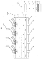
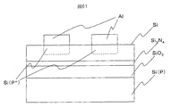
- a selective emitter solar cell (500) having a back surface electric field layer is a semiconductor having an n-type semiconductor layer (12, 12a) and a p-type semiconductor layer (14, 14a) as shown in FIG.
- a light receiving surface side electrode (22) and a protective layer (24) are disposed on the light receiving surface side surface of the semiconductor substrate (10), and the back surface side of the semiconductor substrate (10).
- the back surface side electrode (32) and the protective layer (34) are arrange
- Such a solar cell has a selective emitter layer (12a), thereby causing a problem caused by a high dopant concentration on the light receiving surface side, that is, an increase in reflection on the light receiving side surface due to a high dopant concentration layer, for example. While preventing, the benefit of high dopant concentration at the point of contact with the electrode, i.e. the benefit of, for example, ohmic contact between the electrode and the semiconductor layer, can be achieved.
- such a solar cell (500) can reduce the recombination loss of carriers due to defects near the surface on the back surface side by having the back surface electric field layer (14a).
- Electrons reach the depletion layer between the n-type semiconductor layer and the p-type semiconductor layer, and are caused to flow to the n-type semiconductor layer side due to a potential difference in the depletion layer, thereby generating an electromotive force.
- the dopant concentration in the selective emitter layer (12a) and the back surface field layer (14a) is, for example, about 1 to 2 ⁇ 10 21 atoms / cm 3 .
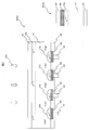
- Patent Documents 2 and 3 show back contact solar cells having a surface electric field layer.
- a back contact solar cell (600) having a surface electric field layer has a semiconductor substrate (10) made of an n-type (or p-type or intrinsic) semiconductor, as shown in FIG.
- the protective layer (24) is disposed on the light receiving surface side surface of the semiconductor substrate (10), and the back surface side electrodes (22, 32) and the protective layer (34) are disposed on the back surface side of the semiconductor substrate (10). Is arranged.
- a back contact layer (where a portion that contacts the electrodes (32, 34) of the semiconductor substrate (10) made of an n-type semiconductor is selectively highly doped n-type or p-type ( 12a, 14a) and the light-receiving surface side of the semiconductor substrate (10) have a surface electric field layer (12b) that is highly doped n-type.
- the n-type back contact layer (12a) highly doped with n and the p-type back contact layer (14a) highly doped with p are alternately arranged on the back surface side.
- the other part is an intrinsic semiconductor region, a region doped with p or n at a low concentration, or a region where a pn junction is formed, and an electromotive force is generated when the region is irradiated with light. The electromotive force generated in this way is taken out by the electrode through the n-type back contact layer (12a) and the p-type back contact layer (14a).
- the solar cell (600) having the surface electric field layer has a layer near the light receiving surface side by having a layer (12b) doped with a high concentration on the light receiving surface side.
- the recombination loss of the carrier due to the defect can be reduced.
- the surface electric field layer (12b) is compared with the relatively lightly doped electrode side of the semiconductor substrate (10) made of an n-type semiconductor. Holes are repelled by the electric field (barrier) created between the surface side of the highly doped surface (12b) and thereby the holes are heavily p-doped (14a) and heavily n-doped. It reaches the depletion layer with respect to the point (12a), and is caused to flow to the p-type semiconductor layer side due to the potential difference in the depletion layer, thereby generating an electromotive force.
- a dopant is injected into a semiconductor layer or substrate in a selected region to form a doped layer in the selected region.
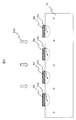
- FET field effect transistor
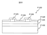
- the field effect transistor (F700) includes a base material (F72), a semiconductor layer (F78), a gate insulating film (F73), a gate electrode (F74), and a source electrode (F75). ) And a drain electrode (F76), and the semiconductor layer (F78) has a doped region (F78b) doped n-type or p-type at a place where the source electrode and drain electrode and the semiconductor layer are in contact with each other. is doing. In such a field effect transistor, this doped region promotes ohmic contact between the semiconductor substrate and the electrode.
- a method in which a dopant source is brought into contact with a layer or a substrate, heat or laser irradiation is performed, and a dopant is injected into the layer or the substrate. It has been.
- a dopant source used here boron silicate glass or phosphorus glass (Patent Document 3), a liquid containing an inorganic dopant (Patent Document 4), or an ink containing silicon and / or germanium nanoparticles (Patent Document 5 and It is known to use 6).
- the semiconductor silicon film is subjected to vacuum processes such as physical vapor deposition (PVD) such as sputtering and chemical vapor deposition (CVD) such as plasma chemical vapor deposition.
- PVD physical vapor deposition
- CVD chemical vapor deposition
- unnecessary portions of the semiconductor silicon film formed on the entire surface of the base material are removed by photolithography or the like to remove the desired pattern. It has been performed to provide a semiconductor silicon film having the same.
- Patent Document 6 proposes forming a semiconductor silicon film using a dispersion containing silicon particles.
- a silicon particle is sintered by irradiating a dry silicon particle film made of silicon particles with a laser.
- the direct drawing technique include a printing method in which a raw material liquid containing a constituent material of a semiconductor silicon film is applied and printed, such as an ink jet printing method and a screen printing method.
- a vacuum process is not required, and a pattern can be formed by direct drawing, so that a semiconductor device can be manufactured easily and at low cost.
- the entire process can be performed at a relatively low temperature, for example, a temperature lower than the glass transition temperature of the polymer material.
- a relatively low temperature for example, a temperature lower than the glass transition temperature of the polymer material.
- an inexpensive general-purpose polymer material can be used for the base material of the semiconductor film, and thereby, an increase in area, flexibility, weight reduction, and cost reduction of the semiconductor device can be expected.
- the process time can be shortened because cooling for each process is not necessary.
- the organic semiconductor film has insufficient performance such as carrier mobility and durability such as stability in the atmosphere as compared with the silicon semiconductor film. It is difficult to make it easier.
- Patent Document 7 discloses a method of forming an InGaZnO 4 film using a nanoparticle dispersion.
- an InGaZnO 4 film dried at room temperature is pretreated with an ultraviolet (UV) ozone cleaner, and then irradiated with a KrF excimer laser (wavelength: 248 nm), whereby a relatively uniform InGaZnO 4 film is formed.
- a crystal film is formed.
- a thin film transistor having a carrier mobility of 1.2 cm 2 / V ⁇ s is manufactured by such a method.
- inorganic compound semiconductor materials such as InGaZnO 4 are very expensive compared to silicon semiconductors due to the problem of raw material availability, and are not practical as general TFT materials.
- Patent Documents 8 and 9 use an organic silicon compound solution containing a high molecular weight low-volatile polysilane compound.
- this low volatility polysilane compound is obtained using cyclopentasilane as a precursor.
- Patent Document 6 proposes forming a semiconductor silicon film using a dispersion containing silicon particles.
- the use of a direct drawing technique for directly drawing a desired pattern of a semiconductor silicon film on a substrate is also being studied.
- Examples of the direct drawing technique include a printing method in which a raw material liquid containing a constituent material of a semiconductor silicon film is applied and printed, such as an ink jet printing method and a screen printing method.
- a vacuum process is not required, and a pattern can be formed by direct drawing, so that a semiconductor device can be manufactured easily and at low cost.
- Patent Document 10 discloses a method of manufacturing a semiconductor silicon film in which columnar crystal grains are adjacent in the minor axis direction by a vapor phase method. Has proposed.
- an amorphous silicon layer is deposited on a base material, and the amorphous silicon layer is crystallized with a laser or the like to form a polysilicon layer.
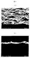
- the silicon crystal when the amorphous silicon layer is crystallized, the silicon crystal may grow abnormally and a convex portion may be formed on the surface of the polysilicon layer.
- Such convex portions on the surface may cause an interlayer short circuit or an interlayer leakage when an insulating layer is deposited thereon, and may cause a contact failure when an electrode is formed thereon. It is preferable to remove. Therefore, in order to remove such convex portions and obtain a flat surface, it has been proposed to perform etching with acid, polishing, and the like (Patent Documents 11 and 12).
- a silicon particle dispersion containing doped silicon particles is applied to the substrate and applied.
- Such a silicon layer also preferably has a flat surface as described above, but a silicon layer obtained by sintering silicon particles generally has a relatively large convex portion on the surface.
- a liquid phase method has been studied as a method for forming a semiconductor film.
- a semiconductor film for a thin film transistor or the like is formed by a low-cost and simple process.
- a liquid phase method has been studied as a method for this.
- the liquid phase method uses a semiconductor material that can be applied, and thus does not require a large-scale apparatus that has been required in the past.
- the use efficiency of raw materials can be increased by application such as ink jetting. Simplification can be achieved.
- the use of an organic semiconductor material has been studied.
- the organic semiconductor film has insufficient performance such as carrier mobility and durability such as stability in the atmosphere as compared with the silicon semiconductor film. It is difficult to make it easier.
- Patent Document 6 proposes to form a semiconductor silicon film using a dispersion containing silicon particles.
- the use of a direct drawing technique for directly drawing a desired pattern of a semiconductor silicon film on a substrate is also being studied.
- Examples of the direct drawing technique include a printing method in which a raw material liquid containing a constituent material of a semiconductor silicon film is applied and printed, such as an ink jet printing method and a screen printing method.
- a vacuum process is not required, and a pattern can be formed by direct drawing, so that a semiconductor device can be manufactured easily and at low cost.
- the entire process can be performed at a relatively low temperature, for example, a temperature lower than the glass transition temperature of the polymer material.
- a relatively low temperature for example, a temperature lower than the glass transition temperature of the polymer material.
- an inexpensive general-purpose polymer material can be used for the base material of the semiconductor film, and thereby, an increase in area, flexibility, weight reduction, and cost reduction of the semiconductor device can be expected.
- the process time can be shortened because cooling for each process is not necessary.
- the organic semiconductor film has insufficient performance such as carrier mobility and durability such as stability in the atmosphere as compared with the silicon semiconductor film. It is difficult to make it easier.
- Patent Document 7 discloses a method of forming an InGaZnO 4 film using a nanoparticle dispersion.
- an InGaZnO 4 film dried at room temperature is pretreated with an ultraviolet (UV) ozone cleaner, and then irradiated with a KrF excimer laser (wavelength: 248 nm), whereby a relatively uniform InGaZnO 4 film is formed.
- a crystal film is formed.
- a thin film transistor having a carrier mobility of 1.2 cm 2 / V ⁇ s is manufactured by such a method.
- inorganic compound semiconductor materials such as InGaZnO 4 are very expensive compared to silicon semiconductors due to the problem of raw material availability, and are not practical as general TFT materials.
- Patent Documents 8 and 9 use an organic silicon compound solution containing a high molecular weight low-volatile polysilane compound.
- this low volatility polysilane compound is obtained using cyclopentasilane as a precursor.
- Patent Document 6 proposes forming a semiconductor silicon film using a dispersion containing silicon particles.
- the use of a direct drawing technique for directly drawing a desired pattern of a semiconductor silicon film on a substrate is also being studied.
- Examples of the direct drawing technique include a printing method in which a raw material liquid containing a constituent material of a semiconductor silicon film is applied and printed, such as an ink jet printing method and a screen printing method.
- a vacuum process is not required, and a pattern can be formed by direct drawing, so that a semiconductor device can be manufactured easily and at low cost.
- a dopant such as phosphorus or boron is implanted into a semiconductor layer or substrate in a selected region to form a diffusion region in the selected region.
- dopants are implanted into a semiconductor layer or substrate in selected regions to form diffusion regions or doped regions in selected regions ( Patent Documents 3 to 6).
- JP 2010-186900 Special table 2009-521805 JP 2010-262979 JP 07-297429 A Special table 2010-519731 Special table 2010-514585 JP 2009-147192 A JP 2004-87546 A (corresponding to Japanese Patent No. 4016419) JP 2010-506001 A JP 2002-270511 A JP-A-2-163935 Japanese Patent Laid-Open No. 2006-261681 US Pat. No. 7,704,866
- the conventional method requires a photolithography step to apply the dopant source to the selected region, requires a step of removing the dopant source after the dopant implantation, and forms the doped layer by diffusion. Therefore, there is a problem that it is difficult to adjust the doping concentration in the depth direction.
- the present invention provides a method of manufacturing a semiconductor device that does not have the above problems.
- the present invention also provides a semiconductor device obtained by the method of the present invention and a dispersion that can be used in the method of the present invention.
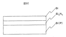
- silicon particles are sintered by heating a dry silicon particle film made of silicon particles.
- a dry silicon particle film made of silicon particles.
- the performance of the substrate and other layers may be deteriorated by heating.
- an object of the present invention is to provide a silicon semiconductor film having excellent semiconductor characteristics from silicon particles, and in particular, to provide a silicon semiconductor film having excellent semiconductor characteristics without using heat treatment at a relatively high temperature. Is to provide from.
- An object of the present invention is to provide a novel semiconductor silicon film, a semiconductor device having such a semiconductor silicon film, and a manufacturing method thereof.
- the present invention provides a semiconductor laminate in which a silicon layer having a flat surface is formed on a substrate, and a method for manufacturing such a semiconductor laminate.
- An object of the present invention is to provide a method for efficiently producing a semiconductor silicon film at a relatively low temperature. More specifically, an object of the present invention is to provide a method for manufacturing a semiconductor stacked body having a semiconductor silicon film having high continuity without requiring an expensive and energy-consuming large-scale apparatus. .
- Another object of the present invention is to provide a semiconductor laminate having a highly continuous semiconductor silicon film, and a semiconductor device having such a semiconductor laminate.
- An object of the present invention is to provide a method for efficiently producing a semiconductor silicon film at a relatively low temperature. More specifically, an object of the present invention is to provide a semiconductor laminate in which a semiconductor film can be formed on a substrate having a relatively low heat resistance such as a plastic substrate without requiring an expensive and energy-consuming large-scale apparatus. It is to provide a manufacturing method.
- an object of the present invention is to provide a semiconductor laminate having a base material having a polymer material and a semiconductor silicon film laminated on the base material.
- an object of the present invention is to provide a method for manufacturing a semiconductor stacked body, which can form a diffusion region in a selected region without using a photolithography process.
- a method for producing a semiconductor device comprising a semiconductor layer or base material comprising a semiconductor element, and a first dopant injection layer on the semiconductor layer or base material, Including the following steps (a) to (c), wherein the crystal orientation of the first dopant injection layer is the same as the crystal orientation of the semiconductor layer or substrate, and / or the concentration of the dopant is 1 ⁇ 10 20 atoms / cm 3 or more at a depth of 0.1 ⁇ m from the surface of the dopant injection layer, and a depth of 0.1 ⁇ m at a depth of 0.3 ⁇ m from the surface of the first dopant injection layer 1/10 or less of Semiconductor device manufacturing method: (A) applying the first dispersion containing the first particles to the first portion of the semiconductor layer or substrate, wherein the first particles include the semiconductor layer or substrate; Consisting essentially of the same element and doped with a p-type or n-type dopant, (B) drying the applied first dispersion to form
- the first portion of the semiconductor layer or base material is doped with the p-type or n-type dopant, and the first unsintered dopant injection layer is sintered to form the semiconductor layer or base material.
- the first dopant injection layer is the same as the crystal orientation of the semiconductor layer or substrate.
- the concentration of the dopant is 1 ⁇ 10 20 atoms / cm 3 or more at a depth of 0.1 ⁇ m from the surface of the first dopant injection layer, and is 0 from the surface of the first dopant injection layer.
- the method according to ⁇ A1> wherein the depth is 1/10 or less of the depth of 0.1 ⁇ m at a depth of 3 ⁇ m.
- the method further includes the following steps (a ′) to (c ′), and the crystal orientation of the second dopant injection layer is the same as the crystal orientation of the semiconductor layer or substrate, and / or the dopant concentration is 1 ⁇ 10 20 atoms / cm 3 or more at a depth of 0.1 ⁇ m from the surface of the second dopant implantation layer, and 0 at a depth of 0.3 ⁇ m from the surface of the second dopant implantation layer.
- the method further includes the following steps (a ′′) to (c ′′), and the crystal orientation of the second dopant injection layer is the same as the crystal orientation of the semiconductor layer or the substrate
- And / or the dopant concentration is 1 ⁇ 10 20 atoms / cm 3 or more at a depth of 0.1 ⁇ m from the surface of the second dopant implantation layer, and is 0 from the surface of the second dopant implantation layer. At a depth of 3 ⁇ m, it is 1/10 or less of a depth of 0.1 ⁇ m.
- the semiconductor layer or It is set as the 2nd dopant injection layer integrated with the base material.
- the semiconductor element is silicon, germanium, or a combination thereof.
- the dispersion is applied by a printing method or spin coating.
- the crystallinity of the particles is 40% or less.
- ⁇ A9> The method according to any one of ⁇ A1> to ⁇ A8>, wherein the average primary particle diameter of the particles is 30 nm or less.
- the dopant is selected from the group consisting of B, Al, Ga, In, Ti, P, As, Sb, or a combination thereof. The method described.
- ⁇ A11> The method according to any one of ⁇ A1> to ⁇ A10>, wherein the particles contain the dopant in an amount of 1 ⁇ 10 20 atoms / cm 3 or more.
- ⁇ A12> The method according to any one of ⁇ A1> to ⁇ A11>, further comprising forming an electrode on the dopant injection layer.
- ⁇ A13> The method according to any one of ⁇ A1> to ⁇ A12>, wherein the semiconductor device is a solar cell.
- ⁇ A14> The method according to ⁇ A13>, wherein the dopant injection layer is for forming a selective emitter layer of a selective emitter solar cell or a back contact layer of a back contact solar cell.
- ⁇ A15> The method according to ⁇ A13> or ⁇ A14>, wherein the dopant injection layer is for forming a back surface field layer or a surface field layer.
- the first dopant injection layer formed by sintering the first particles is disposed in the first portion of the layer or substrate made of a semiconductor element, The first particle consists essentially of the same element as the semiconductor layer or substrate and is doped with a p-type or n-type dopant;
- the first dopant injection layer is integrated with the semiconductor layer or the base material, and the crystal orientation of the first dopant injection layer is the same as the crystal orientation of the semiconductor layer or the base material, and / or
- the dopant concentration is 1 ⁇ 10 20 atoms / cm 3 or more at a depth of 0.1 ⁇ m from the surface of the first dopant injection layer, and 0.3 ⁇ m from the surface of the first dopant injection layer.
- the depth is 1/10 or less of the depth of 0.1 ⁇ m.
- Semiconductor device. ⁇ A18> The semiconductor device according to ⁇ A17>, wherein the crystal orientation of the first dopant injection layer is the same as the crystal orientation of the semiconductor layer or substrate.
- the concentration of the dopant is 1 ⁇ 10 20 atoms / cm 3 or more at a depth of 0.1 ⁇ m from the surface of the first dopant injection layer, and is 0 from the surface of the first dopant injection layer.
- the semiconductor device according to ⁇ A17> which is 1/10 or less of a depth of 0.1 ⁇ m at a depth of 3 ⁇ m.
- the second dopant injection layer formed by sintering the second particles is disposed in the second portion of the semiconductor layer or the base material,
- the second particle consists essentially of the same element as the semiconductor layer or substrate and is doped with a different type of dopant than the dopant of the first particle;
- the second dopant injection layer is integrated with the semiconductor layer or substrate, and the crystal orientation of the second dopant injection layer is the same as the crystal orientation of the semiconductor layer or substrate, and / or
- the dopant concentration is 1 ⁇ 10 20 atoms / cm 3 or more at a depth of 0.1 ⁇ m from the surface of the second dopant implantation layer, and 0.3 ⁇ m from the surface of the second dopant implantation layer.
- the depth is 1/10 or less of the depth of 0.1 ⁇ m.
- ⁇ A21> The semiconductor device according to any one of ⁇ A17> to ⁇ A20>, wherein the semiconductor element is silicon, germanium, or a combination thereof.
- ⁇ A22> The semiconductor device according to any one of ⁇ A17> to ⁇ A21>, wherein an electrode is formed on the dopant injection layer.
- ⁇ A23> The semiconductor device according to any one of ⁇ A17> to ⁇ A22>, which is a solar cell.
- ⁇ A24> The semiconductor device according to ⁇ A23>, wherein the dopant injection layer is for forming a selective emitter layer of a selective emitter solar cell or a back contact layer of a back contact solar cell.
- ⁇ A25> The semiconductor device according to ⁇ A23> or ⁇ A24>, wherein the dopant injection layer is for forming a back surface field layer or a surface field layer.
- ⁇ A26> The semiconductor device according to any one of ⁇ A17> to ⁇ A22>, which is a thin film transistor.
- ⁇ A27> A dispersion containing particles, wherein the particles consist essentially of a semiconductor element having a crystallinity of 40% or less and being n- or p-doped.
- ⁇ A28> A dispersion containing particles, wherein the particles have an average primary particle diameter of 30 nm or less and essentially consist of an n- or p-doped semiconductor element.
- ⁇ A29> The dispersion according to ⁇ A27> or ⁇ A28>, wherein the semiconductor element is silicon, germanium, or a combination thereof.
- ⁇ B1> The amount of the desorbing gas composed of unsintered silicon particles and desorbed when heated in an inert gas atmosphere at a pressure of 1 atm and a temperature of 600 ° C.
- ⁇ B2> The unsintered silicon particle film according to ⁇ B1>, wherein the desorbing gas is selected from the group consisting of a silane compound, an organic solvent, and a combination thereof.
- ⁇ B3> The unsintered silicon particle film according to ⁇ B1> or ⁇ B2>, which has a thickness of 50 to 2000 nm.
- ⁇ B4> The unsintered silicon particle film according to any one of ⁇ B1> to ⁇ B3>, wherein the silicon particles are silicon particles obtained by a laser pyrolysis method.
- ⁇ B5> (a) a step of applying a silicon particle dispersion containing a dispersion medium and silicon particles dispersed in the dispersion medium on a substrate to form a silicon particle dispersion film; (B) drying the silicon particle dispersion film to form a dry silicon particle film; and (c) sintering the dry silicon particle film at a temperature of 300 ° C. to 900 ° C.
- the manufacturing method of a non-sintered silicon particle film including the process of forming a silicon particle film.
- ⁇ B6> The method according to ⁇ B5>, wherein in the step (c), the baking is performed at a temperature of 500 ° C. or higher.
- ⁇ B7> The method according to ⁇ B5> or ⁇ B6>, wherein the baking is performed at a temperature of 800 ° C. or lower in the step (c).
- ⁇ B8> A semiconductor silicon film made of silicon particles sintered together and substantially free of carbon atoms.
- ⁇ B9> The semiconductor silicon film according to ⁇ B8>, which is not subjected to a heat treatment at a temperature exceeding 1,000 ° C.
- ⁇ B10> A semiconductor device having the semiconductor silicon film according to ⁇ B8> or ⁇ B9> as a semiconductor film.
- ⁇ B11> The semiconductor device according to ⁇ B10>, which is a solar battery.
- ⁇ B12> a step of obtaining an unsintered silicon particle film by the method according to any one of ⁇ B5> to ⁇ B7> above,
- Semiconductor silicon comprising a step of irradiating the unsintered silicon particle film with light or applying heat to sinter the silicon particles in the unsintered silicon particle film, thereby forming a semiconductor silicon film A method for producing a membrane.
- ⁇ B13> The silicon in the green silicon particle film is irradiated with light or heat applied to the green silicon particle film according to any one of the above ⁇ B1> to ⁇ B4>.
- a method for producing a semiconductor silicon film comprising a step of sintering particles.
- ⁇ B14> The method according to ⁇ B12> or ⁇ B13>, wherein the sintering is performed by light irradiation using a laser.
- ⁇ B15> The method according to any one of ⁇ B12> to ⁇ B14>, wherein the sintering is performed in a non-oxidizing atmosphere.
- ⁇ C1> A semiconductor silicon film in which a plurality of elongated silicon particles are adjacent in the minor axis direction, and the elongated silicon particles are a sintered body of a plurality of silicon particles.
- ⁇ C2> The semiconductor silicon film according to ⁇ C1>, wherein at least a part of the elongated silicon particles has a minor axis diameter of 100 nm or more.
- ⁇ C3> The semiconductor silicon film according to ⁇ C1> or ⁇ C2>, wherein at least a part of the elongated silicon particles has an aspect ratio of more than 1.2.
- ⁇ C4> A semiconductor device comprising the semiconductor silicon film according to any one of ⁇ C1> to ⁇ C3> above.
- ⁇ C5> The semiconductor device according to ⁇ C4>, which is a solar cell.
- ⁇ C6> A method for producing a semiconductor silicon film in which a plurality of elongated silicon particles are adjacent in the minor axis direction, (A) A first silicon particle dispersion containing a first dispersion medium and first silicon particles dispersed in the first dispersion medium is applied onto a substrate to form first silicon Forming a particle dispersion film, (B) drying the first silicon particle dispersion film to form a first unsintered semiconductor silicon film; and (c) irradiating the first unsintered semiconductor silicon film with light.
- ⁇ C7> The method according to ⁇ C6>, wherein the average primary particle diameter of the silicon particles is 100 nm or less.
- ⁇ C8> The method according to ⁇ C6> or ⁇ C7>, wherein the silicon particles are silicon particles obtained by a laser pyrolysis method.
- ⁇ C9> The method according to any one of ⁇ C6> to ⁇ C8>, wherein the unsintered semiconductor silicon film has a thickness of 50 to 2000 nm.
- ⁇ C10> The method according to any one of ⁇ C6> to ⁇ C9>, wherein the light irradiation is performed using a laser.
- ⁇ C11> The method according to any one of ⁇ C6> to ⁇ C10>, wherein the light irradiation is performed in a non-oxidizing atmosphere.
- ⁇ C12> A semiconductor silicon film obtained by the method according to any one of ⁇ C6> to ⁇ C11> above.
- ⁇ C13> A method for producing a semiconductor device, comprising producing a semiconductor silicon film by the method according to any one of ⁇ C6> to ⁇ C11> above.
- ⁇ C14> A semiconductor device obtained by the method according to ⁇ C13>.
- ⁇ D1> A substrate and a composite silicon film on the substrate, and the composite silicon film is a first silicon layer derived from amorphous silicon, and a second derived from silicon particles on the first silicon layer.
- ⁇ D2> The semiconductor laminate according to ⁇ D1>, wherein the height of the convex portion of the composite silicon layer is 100 nm or less.
- ⁇ D3> A semiconductor device having the semiconductor laminate according to ⁇ D1> or ⁇ D2>.
- ⁇ D4> The semiconductor device according to ⁇ D3>, which is a solar battery.
- ⁇ D5> The semiconductor device according to ⁇ D4>, wherein the composite silicon layer is for forming a selective emitter layer of a selective emitter solar cell or a back contact layer of a back contact solar cell.
- ⁇ D6> The semiconductor device according to ⁇ D4> or ⁇ D5>, wherein the composite silicon layer is for forming a back surface field layer or a surface field layer.
- ⁇ D7> The semiconductor device according to ⁇ D3>, which is a field effect transistor.
- ⁇ D8> Manufacturing method of semiconductor laminated body including the following steps: (A) forming an amorphous silicon layer on the substrate; (B) applying a silicon particle dispersion on the amorphous silicon layer and drying to form an untreated laminate in which the silicon particle layer is laminated on the amorphous silicon layer; A process of forming a composite silicon layer having a first silicon layer derived from amorphous silicon and a second silicon layer derived from silicon particles on the first silicon layer by irradiating the fired laminate with light.
- ⁇ D9> The method according to ⁇ D8>, wherein the amorphous silicon layer has a thickness of 300 nm or less.
- ⁇ D10> The method according to ⁇ D8> or ⁇ D9>, wherein the silicon particle layer has a thickness of 300 nm or less.
- ⁇ D11> The method according to any one of ⁇ D8> to ⁇ D10>, wherein an average primary particle diameter of the silicon particles is 100 nm or less.
- ⁇ D12> The method according to any one of ⁇ D8> to ⁇ D11>, wherein the light irradiation is performed using a laser.
- ⁇ D13> A semiconductor laminate obtained by the method according to any one of ⁇ D8> to ⁇ D12> above.
- ⁇ D14> A method for producing a semiconductor device, comprising producing a semiconductor laminate by the method according to any one of ⁇ D8> to ⁇ D12> above.
- ⁇ D15> A semiconductor device obtained by the method according to ⁇ D14>.
- a method for producing a semiconductor laminate having a substrate and a semiconductor silicon film laminated on the substrate (A) applying a silicon particle dispersion containing a dispersion medium and silicon particles dispersed in the dispersion medium on the surface of the substrate to form a silicon particle dispersion film; (B) drying the silicon particle dispersion film to form an unsintered silicon film; and (c) irradiating the unsintered silicon film with light to form the unsintered silicon film. Sintering silicon particles, thereby forming a semiconductor silicon film; And a contact angle of the molten silicon with respect to the surface of the substrate is 70 degrees or less.
- ⁇ E2> The method according to ⁇ E1>, wherein the surface of the substrate is provided by a material selected from the group consisting of carbide, nitride, carbonitride, and combinations thereof.
- ⁇ E3> The surface of the substrate according to ⁇ E2>, wherein the surface of the substrate is provided by a material selected from the group consisting of silicon carbide, silicon nitride, silicon carbonitride, graphite, and combinations thereof.
- Method. ⁇ E4> The items ⁇ E1> to ⁇ E3>, wherein the substrate has a substrate body and a surface layer, and the surface layer is made of a material having a contact angle of 70 degrees or less with molten silicon. The method as described in any one of.
- ⁇ E5> The method according to any one of ⁇ E1> to ⁇ E3>, wherein the entire base material is made of the same material as the surface of the base material.
- ⁇ E6> The method according to any one of ⁇ E1> to ⁇ E5>, wherein the silicon particles have an average primary particle diameter of 100 nm or less.
- ⁇ E7> The method according to any one of ⁇ E1> to ⁇ E6>, wherein the silicon particles are silicon particles obtained by a laser pyrolysis method.
- ⁇ E8> The method according to any one of ⁇ E1> to ⁇ E7>, wherein the light irradiation is performed in a non-oxidizing atmosphere.
- ⁇ E9> The method according to any one of ⁇ E1> to ⁇ E8>, wherein the light irradiation is performed using a laser.
- ⁇ E10> The method according to ⁇ E9>, wherein the laser has a wavelength of 600 nm or less.
- ⁇ E11> The method according to any one of ⁇ E1> to ⁇ E10>, wherein the light irradiation is performed using pulsed light.
- ⁇ E12> A method for producing a semiconductor device, comprising producing a semiconductor laminate by the method according to any one of ⁇ E1> to ⁇ E11> above.
- ⁇ E13> A semiconductor laminate obtained by the method according to any one of ⁇ E1> to ⁇ E11> above.
- ⁇ E14> A semiconductor device obtained by the method according to ⁇ E12>.
- ⁇ E15> having a base material, and a semiconductor silicon film laminated on the surface of the base material, The semiconductor silicon film is made of a plurality of silicon particles sintered together, and the contact angle of the molten silicon to the surface of the base material is 70 degrees or less, Semiconductor stack.
- ⁇ E16> The semiconductor laminate according to ⁇ E15>, wherein the semiconductor silicon film has a thickness of 50 to 500 nm.
- ⁇ E17> A semiconductor device comprising the semiconductor laminate according to ⁇ E15> or ⁇ E16>.
- ⁇ E18> A method for producing a semiconductor laminate having a substrate and a semiconductor silicon film laminated on the substrate, (A) applying a silicon particle dispersion containing a dispersion medium and silicon particles dispersed in the dispersion medium on the surface of the substrate to form a silicon particle dispersion film; (B) drying the silicon particle dispersion film to form an unsintered silicon film; and (c) irradiating the unsintered silicon film with light to form the unsintered silicon film. Sintering silicon particles, thereby forming a semiconductor silicon film; And the surface of the substrate is provided by a material selected from the group consisting of silicon carbide, silicon nitride, silicon carbonitride, graphite, and combinations thereof.
- ⁇ E19> having a base material, and a semiconductor silicon film laminated on the surface of the base material,
- the semiconductor silicon film is made of a plurality of silicon particles sintered together, and the surface of the substrate is made of silicon carbide, silicon nitride, silicon carbonitride, graphite, and combinations thereof.
- a material selected from the group Semiconductor stack.
- ⁇ F1> (a) a step of applying a silicon particle dispersion containing a dispersion medium and silicon particles dispersed in the dispersion medium on a substrate to form a silicon particle dispersion film; (B) drying the silicon particle dispersion film to form an unsintered semiconductor silicon film; and (c) irradiating the unsintered semiconductor silicon film with light to form the unsintered semiconductor silicon film. Sintering the silicon particles therein, thereby forming a semiconductor silicon film; The manufacturing method of the semiconductor laminated body which has a semiconductor silicon film laminated
- ⁇ F2> The method according to ⁇ F1>, wherein the substrate has a polymer material.
- ⁇ F3> The method according to ⁇ F1> or ⁇ F2>, wherein the polymer material has a glass transition temperature of 300 ° C. or lower.
- ⁇ F4> The method according to any one of ⁇ F1> to ⁇ F3>, wherein the silicon particles have an average primary particle diameter of 100 nm or less.
- ⁇ F5> (a ′) A second silicon particle dispersion containing the second dispersion medium and the second silicon particles dispersed in the second dispersion medium was obtained in the step (c).
- Doped process (B ′′) drying the third silicon particle dispersion film to form a green dopant injection film; and (c ′′) irradiating the green dopant injection film with light, Sintering the third silicon particles in the unsintered dopant implantation film to form a dopant implantation film, and doping selected regions of the semiconductor silicon film with the p-type or n-type dopant;
- ⁇ F8> The method according to any one of ⁇ F1> to ⁇ F7>, wherein the particles contain the dopant in an amount of 1 ⁇ 10 20 atoms / cm 3 or more.
- ⁇ F9> The method according to any one of ⁇ F1> to ⁇ F8>, further comprising forming an electrode on the dopant injection film.
- ⁇ F10> The method according to any one of ⁇ F1> to ⁇ F9>, wherein the finally obtained semiconductor silicon film has a carrier mobility of 0.1 cm 2 / V ⁇ s or more.
- ⁇ F11> on the finally obtained the semiconductor silicon film - off ratio is 10 2 or more, the ⁇ F1> ⁇ ⁇ F10> method according to any one of claims.
- ⁇ F12> The method according to any one of ⁇ F1> to ⁇ F11>, wherein the silicon particles are silicon particles obtained by a laser pyrolysis method.
- ⁇ F13> The method according to any one of ⁇ F1> to ⁇ F12>, wherein the unsintered semiconductor silicon film has a thickness of 50 to 2000 nm.
- ⁇ F14> The light irradiation is performed using pulsed light, and the irradiation energy of the pulsed light is 15 mJ / (cm 2 ⁇ shot) to 250 mJ / (cm 2 ⁇ shot).
- the method according to any one of items ⁇ 1> to ⁇ F13> The method according to any one of items ⁇ 1> to ⁇ F13>.
- ⁇ F15> The method according to any one of ⁇ F1> to ⁇ F14>, wherein the light irradiation is performed using pulsed light, and the number of times of irradiation of the pulsed light is 5 to 100 times.
- the method of. ⁇ F16> Any one of the above ⁇ F1> to ⁇ F15>, wherein the light irradiation is performed using pulsed light, and the irradiation time of the pulsed light is 200 nanoseconds / shot or less.
- ⁇ F17> The method according to any one of ⁇ F1> to ⁇ F16>, wherein the light irradiation is performed using a laser.
- ⁇ F18> The method according to ⁇ F17>, wherein the laser has a wavelength of 600 nm or less.
- ⁇ F19> The method according to any one of ⁇ F1> to ⁇ F18>, wherein the light irradiation is performed in a non-oxidizing atmosphere.
- ⁇ F20> A method for producing a semiconductor device, comprising producing a semiconductor laminate by the method according to any one of ⁇ F1> to ⁇ F19>.
- ⁇ F21> A semiconductor laminate obtained by the method according to any one of ⁇ F1> to ⁇ F19>.
- ⁇ F22> A semiconductor device obtained by the method according to ⁇ F20>.
- the substrate has a polymer material;
- the semiconductor silicon film is made of a plurality of silicon particles sintered together, and the carrier mobility of the semiconductor silicon film is 1.0 cm 2 / V ⁇ s or more.
- ⁇ F25> a semiconductor laminate having a substrate, a semiconductor silicon film laminated on the substrate, and a dopant injection film laminated on the semiconductor silicon film,
- the semiconductor silicon film is made of a plurality of silicon particles sintered together
- the dopant injection film is made of a plurality of silicon particles sintered together,
- ⁇ F26> A semiconductor device comprising the semiconductor laminate according to any one of ⁇ F23> to ⁇ F25> above.
- the dopant concentration is 1 ⁇ 10 20 atoms / cm 3 or more at a depth of 0.1 ⁇ m from the surface of the first dopant injection layer. And at a depth of 0.3 ⁇ m, especially 0.2 ⁇ m from the surface of the first dopant injection layer, which is 1/10 or less of the depth of 0.1 ⁇ m, that is, the doping concentration gradient is large, thereby
- a high doping concentration is achieved while reducing the thickness of the portion with a high doping concentration, for example, suppression of light absorption by a high dopant concentration layer, improvement of characteristics when used as a back surface field layer or a surface field layer Etc. can be achieved.
- dispersion of the present invention can be preferably used for the method of the present invention.
- the semiconductor silicon film of the present invention having a low carbon content, good semiconductor characteristics can be provided.
- the unsintered silicon particle film and the semiconductor silicon film of the present invention can be obtained.
- the semiconductor silicon film of the present invention in which a plurality of elongated silicon particles are adjacent in the minor axis direction, good carrier mobility can be achieved in a device in which carriers flow in the thickness direction of the semiconductor silicon film. This is because such a semiconductor silicon film has few or substantially no grain boundaries in the thickness direction of the semiconductor silicon film, that is, the long axis direction of the elongated silicon particles.
- the semiconductor silicon film of the present invention can be obtained by a liquid phase method.
- the composite silicon layer can have a flat surface, and therefore, a semiconductor device having good characteristics can be obtained when an insulating layer, an electrode, or the like is deposited thereon. Moreover, in the method of the present invention for producing a semiconductor laminate, the composite silicon layer on the substrate can have a flat surface without an additional step of removing surface irregularities.
- a semiconductor silicon film can be produced efficiently at a relatively low temperature. More specifically, according to the method of the present invention, it is possible to manufacture a semiconductor stacked body having a semiconductor silicon film having high continuity without requiring an expensive and energy-consuming large-scale apparatus.
- the semiconductor laminate of the present invention has a semiconductor silicon film with high continuity, thereby providing preferable semiconductor characteristics.
- a semiconductor laminated body having desired semiconductor characteristics can be formed by a simple method. Specifically, according to the method of the present invention, it is possible to manufacture a semiconductor laminated body having good semiconductor characteristics at a low temperature as compared with the process temperature of the prior art.
- the semiconductor laminate of the present invention can be used for a semiconductor device that is preferable in terms of semiconductor characteristics, cost, flexibility, and / or lightness.
- FIG. 3 is an FE-SEM (field emission scanning electron microscope) photograph of the laminate of Example A1.
- (a) is a photograph viewed obliquely from above, and (b) is a side sectional photograph.
- It is a TEM (transmission electron microscope) photograph about the laminated body of Example A1.
- FIG. 11 is an enlarged TEM photograph of a region indicated by B-1 in FIG.
- FIG. 11 is an enlarged TEM photograph of a region indicated by B-2 in FIG.
- FIG. 11 is an enlarged TEM photograph of a region indicated by B-3 in FIG.
- (a) is a photograph viewed obliquely from above, and (b) is a side sectional photograph. It is a figure which shows the result of Dynamic SIMS (dynamic secondary ion mass spectrometry) about the laminated body of Example A2. It is a figure which shows the SCM (scanning capacitance microscope) photograph (a) about the laminated body of Example A1, and the synthetic
- (a) is a front view and (b) is a top view.
- FIG. 6 is a diagram showing the evaluation results of IV (current-voltage) characteristics of the solar cell created in Comparative Example 1. It is a figure for demonstrating the measuring method of the crystallinity degree in this invention. It is a figure which shows the result of Dynamic SIMS (dynamic secondary ion mass spectrometry) about the laminated body of Example A3.
- 3 is an FE-SEM (field emission scanning electron microscope) photograph of the laminate of Example A3.
- (a) is a photograph viewed obliquely from above, and (b) is a side sectional photograph. It is a TEM (transmission electron microscope) photograph about the laminated body of Example A3. It is an enlarged TEM photograph about the area
- FIG. It is a figure which shows the result of Dynamic SIMS (dynamic secondary ion mass spectrometry) about the laminated body of the comparative example 2.
- FIG. It is a figure which shows the manufacturing method of the non-sintered silicon particle film of this invention, and the semiconductor silicon film of this invention. It is a figure which shows the manufacturing method of the conventional semiconductor silicon film. It is a figure which shows the temperature desorption gas analysis method (TDS: Thermal Desorption Spectroscopy) result about a dry silicon particle film.
- TDS Thermal Desorption Spectroscopy
- FIG. 52 (a) is a photograph of the side section observed from obliquely above
- FIG. 52 (b) is a photograph of the side section observed from the side.
- FIG. 52 (a) is a photograph of the side section observed from obliquely above
- FIG. 52 (b) is a photograph of the side section observed from the side.
- FIG. 52 (a) is a photograph of the side section observed from obliquely above
- FIG. 52 (b) is a photograph of the side section observed from the side.
- FIG. 52 (a) is a photograph of the side section observed from obliquely above
- FIG. 52 (b) is a photograph of the side section observed from the side.
- FIG. 52 (a) is a photograph of the side section observed from obliquely above
- FIG. 52 (b) is a photograph of the side section observed from the side.
- FIG. 52 (a) is a photograph of the side section observed from obliquely above
- FIG. 55A is a photograph of the side section observed from obliquely above
- FIG. 55B is a photograph of the side section observed from the side. It is a field emission scanning electron microscope (FE-SEM) photograph of the semiconductor silicon film of Reference Example C2.
- FIG. 56 is a photograph of the side cross section observed from the side.
- FIG. 57B is a diagram for explaining the method of the present invention for producing a semiconductor laminate
- FIG. 57B is a diagram for explaining a method for producing a semiconductor laminate by irradiating a single amorphous silicon layer with light
- FIG. 57 (c) is a diagram for explaining a method of manufacturing a semiconductor stacked body by irradiating a single silicon particle layer with light.
- FIG. 4 is an FE-SEM (field emission scanning electron microscope) photograph of the semiconductor stacked body of Example D1.
- (a) is a photograph viewed obliquely from above, and (b) is a side sectional photograph.
- 6 is an FE-SEM (field emission scanning electron microscope) photograph of the semiconductor laminate of Comparative Example D1.
- (a) is a photograph viewed obliquely from above, and (b) is a side sectional photograph.
- 6 is a diagram showing a field effect transistor (FET) having a bottom gate / top contact structure manufactured in Example 3.
- FIG. 10 It is a figure which shows the field effect transistor (FET) of the bottom gate / bottom contact structure manufactured in Examples F6-F8.
- 10 is a diagram showing a field effect transistor (FET) having a bottom gate / top contact structure manufactured in Example 9.
- FIG. It is a figure for demonstrating the field effect transistor of this invention. It is a figure for demonstrating the conventional field effect transistor of this invention.
- dispersion the values dispersion of particles such as silicon particles (sigma 2) is the particle size of each particle, x 1, x 2, x 3, ..., when the x n, as determined by the following formula Is:
- the average primary particle size of the particles is determined by directly measuring the particle size based on the photographed image by observation with a scanning electron microscope (SEM), a transmission electron microscope (TEM), and the like. By analyzing a particle group consisting of several hundreds or more, the number average primary particle diameter can be obtained.
- SEM scanning electron microscope
- TEM transmission electron microscope
- the average primary particle size of silicon particles is measured by TEM, image analysis is performed at a magnification of 100,000, and the average primary particle size of the silicon particle dispersion is based on a set of 500 or more. And / or variance was calculated.
- the method of the present invention for producing a semiconductor device having a semiconductor layer or substrate comprising a semiconductor element and a first dopant injection layer on the semiconductor layer or substrate includes the following steps (a) to (c): (A) applying the first dispersion containing the first particles to the first location of the semiconductor layer or substrate, wherein the first particles are the same element as the semiconductor layer or substrate; And is doped with a p-type or n-type dopant, (B) drying the applied first dispersion to form a first unsintered dopant injection layer; and (c) irradiating the first unsintered dopant injection layer with light, thereby producing a semiconductor.
- the crystal orientation of the first dopant injection layer is the same as the crystal orientation of the semiconductor layer or the substrate. In this case, trapping of carriers at the interface between the dopant injection layer and the semiconductor layer or the substrate can be suppressed.
- the semiconductor device of the present invention when an electrode is further formed on the dopant injection layer, it is possible to promote the movement of carriers reaching the electrode from the semiconductor layer or the base material via the dopant injection layer.
- the semiconductor device of the present invention when the semiconductor device of the present invention is a solar cell, the power generation efficiency can be improved, and when the semiconductor device of the present invention is a thin film transistor, the on-off ratio and the like can be improved. Semiconductor characteristics can be improved.
- the dopant concentration is 1 ⁇ 10 20 atoms / cm 3 or more, particularly 5 ⁇ 10 5 at a depth of 0.1 ⁇ m from the surface of the first dopant injection layer. Depth of 0.1 ⁇ m at 20 atoms / cm 3 or more, more particularly 1 ⁇ 10 21 atoms / cm 3 or more and 0.3 ⁇ m from the surface of the first dopant injection layer, particularly 0.2 ⁇ m. 1/10 or less, particularly 1/100 or less, more particularly 1/1000 or less.
- the semiconductor device of the present invention is a back contact type solar cell and the dopant injection layer is formed on the entire light receiving surface side surface to form the surface electric field layer, the power generation efficiency can be improved.
- an n-type semiconductor layer (12, 12a) and a p-type semiconductor layer (14, 14a) are provided.
- a light receiving surface side electrode (22) and a protective layer (24) are disposed on the light receiving surface side surface of the semiconductor substrate (10), and the back surface of the semiconductor substrate (10).
- the back surface side electrode (32) and the protective layer (34) are arrange
- the portion of the n-type semiconductor layer (12, 12a) in contact with the electrode (22) is increased in dopant concentration by the n-type dopant derived from the dopant injection layer (52),
- the selective emitter layer (12a) is formed.
- the semiconductor substrate (10) may be a semiconductor silicon film, particularly a semiconductor silicon film formed by sintering a plurality of silicon particles.
- the dopant injection layer (52) may be removed after the dopant is injected into the n-type semiconductor layer (12a).
- this solar cell (500a) has a back surface electric field layer (14a) formed by highly doping the back surface side of the p-type semiconductor layers (14, 14a).
- the back surface electric field layer (14a) of this solar cell has a dopant concentration increased by a p-type dopant derived from the dopant injection layer (70) obtained by the method of the present invention, as shown in the partial diagram 500b of FIG. It can also be formed.
- the back contact solar cell (600a) obtained by the method of the present invention has a semiconductor substrate (10) made of an n-type (or p-type) semiconductor as shown in FIG.
- the protective layer (24) is disposed on the light receiving surface side surface of (10), and the back surface side electrodes (22, 32) and the protective layer (34) are disposed on the back surface surface of the semiconductor substrate (10). .
- the portions of the semiconductor substrate (10) made of an n-type semiconductor that are in contact with the electrodes (32, 34) are n-type and p-type derived from the dopant injection layer (52, 62).
- the dopant concentration is increased by the dopant to form back contact layers (12a, 14a).
- the semiconductor substrate (10) may be a semiconductor silicon film, particularly a semiconductor silicon film formed by sintering a plurality of silicon particles.
- the dopant implantation films (52, 62) may be removed after the dopant is implanted into the back contact layers (12a, 14a).
- the light-receiving surface side of the semiconductor substrate (10) has a surface electric field layer (12b) that is highly doped n-type.
- the surface electric field layer (12b) of the solar cell (600a) has a dopant concentration due to the n-type dopant derived from the dopant injection layer (80) obtained by the method of the present invention, as shown in the partial view 600b of FIG. Can also be formed.
- a protective layer (24) is formed (FIG. 5), an electrode (22) is formed thereon, and this electrode reaches the dopant injection layer (52) by thermal diffusion. it can.
- the first particle doped with the p-type or n-type dopant is used to form the first dopant injection layer, and the dopant of the first particle is
- the second dopant injection layer can also be formed using second particles doped with a different type of dopant.
- the method of the present invention further includes the following steps (a ′) to (c ′), and the crystal orientation of the second dopant injection layer is the same as the crystal orientation of the semiconductor layer or substrate.
- / or the concentration of the dopant is 1 ⁇ 10 20 atoms / cm 3 or more at a depth of 0.1 ⁇ m from the surface of the second dopant implantation layer, and 0.3 ⁇ m from the surface of the second dopant implantation layer, In particular, at a depth of 0.2 ⁇ m, it can be 1/10 or less of a depth of 0.1 ⁇ m: (A ′)
- Applying a second dispersion containing second particles wherein the second particles consist essentially of the same elements as the semiconductor layer or substrate and are the dopants of the first particles Doped with different types of dopants, (B ′)
- the particles doped with the p-type dopant and the particles doped with the n-type dopant are sintered together by light irradiation or collectively dried, and light irradiation is performed. It is also possible to sinter by. Such a process may be beneficial to shorten the manufacturing process. Also, in this case, applying the dispersion without using photolithography, using a printing method such as inkjet printing or screen printing, the treatment can be particularly beneficial to shorten the manufacturing process. .
- the method of the present invention further includes the following steps (a ′′) to (c ′′) after the step (c), and the crystal orientation of the second dopant injection layer is the crystal of the semiconductor layer or the substrate.
- the crystal orientation of the second dopant injection layer is the crystal of the semiconductor layer or the substrate.
- the concentration of dopant is 1 ⁇ 10 20 atoms / cm 3 or more at a depth of 0.1 ⁇ m from the surface of the second dopant implantation layer, and from the surface of the second dopant implantation layer At a depth of 0.3 ⁇ m, especially 0.2 ⁇ m, it can be 1/10 or less of a depth of 0.1 ⁇ m: (A ′′) applying a second dispersion containing second particles to a second location of the semiconductor layer or substrate, wherein the second particles are identical to the semiconductor layer or substrate.
- the second selected portion of the semiconductor layer or substrate is doped with a p-type or n-type dopant and the second unsintered dopant injection layer is sintered to be integrated with the semiconductor layer or substrate.
- a dopant injection layer is used to form a second unsintered dopant injection layer.
- the method of the present invention can be repeated to form a dopant injection layer for injecting a p-type dopant and a dopant injection layer for injecting an n-type dopant.
- the description relating to the first dopant injection layer can be referred to.
- the fact that the crystal orientation of the dopant injection layer is the same as the crystal orientation of the semiconductor layer or the base material is determined by analysis using a transmission electron microscope (TEM). Or, there is no disorder of the crystal lattice between the substrate and the diffraction line of the dopant injection layer coincides with the diffraction line of the semiconductor layer or the substrate in the analysis by electron diffraction (ED: Electron Diffraction). Can be confirmed.
- TEM transmission electron microscope
- any semiconductor layer or substrate comprising a semiconductor element can be used.
- the semiconductor layer or base material made of a semiconductor element include a silicon wafer, a gallium wafer, an amorphous silicon layer, an amorphous gallium layer, a crystalline silicon layer, and a crystalline gallium layer.
- silicon, germanium, or a combination thereof can be used as the semiconductor element.
- the application of the dispersion in steps (a), (a ′) and (a ′′) of the method of the present invention for producing a semiconductor device is particularly limited as long as the dispersion can be applied with a desired thickness and uniformity.
- the thickness of the unsintered film obtained when the dispersion film is dried is 50 nm or more, 100 nm or more, or 200 nm or more, and is 2000 nm or less, 1000 nm or less, 500 nm or less, or 300 nm or less.
- FET field effect transistor
- the thickness of an unsintered film is 100 nm or more and 200 nm or more, and is 2000 nm or less, 1000 nm or less, 500 nm or less, or 300 nm or less.
- the thickness of the green film is not particularly limited.
- the dispersion medium of the dispersion is not limited as long as the object and effect of the present invention are not impaired, and therefore, for example, an organic solvent that does not react with the particles used in the present invention can be used.
- the dispersion medium is a non-aqueous solvent such as alcohol, alkane, alkene, alkyne, ketone, ether, ester, aromatic compound, or nitrogen-containing ring compound, particularly isopropyl alcohol (IPA), N-methyl-2. - May be pyrrolidone (NMP) or the like.
- glycol (dihydric alcohol) like ethylene glycol can also be used as alcohol.
- the dispersion medium is preferably a dehydrated solvent in order to suppress oxidation of the particles used in the present invention.
- the particles of the dispersion are particles made of the same element as the semiconductor layer or base material made of a semiconductor element and doped with a p-type or n-type dopant, the dispersion is not limited unless the object and effect of the present invention are impaired. It is not something.
- particles for example, silicon particles or germanium particles as shown in Patent Documents 5 and 6 can be used.
- examples of the silicon particles or germanium particles include silicon particles or germanium particles obtained by a laser pyrolysis method, particularly a laser pyrolysis method using a CO 2 laser.
- the particles of the dispersion have a relatively low crystallinity of the particles and / or a relatively small particle size, so that the particles are melted and sintered by light irradiation, and the resulting dopant injection layer is formed. It may be preferable to integrate with the semiconductor layer or substrate and to make the crystal orientation of the dopant injection layer the same as the crystal orientation of the semiconductor layer or substrate.
- the crystallinity of the particles is preferably 40% or less, 30% or less, 20% or less, 10% or less, or 5% or less.
- the crystallinity is a value determined based on Raman spectroscopy. Specifically, for example, for silicon particles, a peak derived from silicon is detected at a wavelength of 400 to 560 cm ⁇ 1 , and a peak derived from a silicon crystal part is detected from 500 to 540 cm ⁇ 1 . Therefore, as shown in FIG. 34, the ratio of the peak area derived from the silicon crystal part (FIG. 34B) to the total peak area derived from silicon (FIGS. 34A and 34B) is calculated. By doing so, the crystallinity is determined. Incidentally, all the peak areas derived from the silicon (FIG.
- the average primary particle diameter of the particles is preferably 1 nm or more, or 3 nm or more, and is preferably 100 nm or less, 30 nm or less, 20 nm or less, or 10 nm or less.
- the dopant doping the particles of the dispersion may be either a p-type or n-type dopant, for example, boron (B), aluminum (Al), gallium (Ga), indium (In), titanium (Ti ), Phosphorus (P), arsenic (As), antimony (Sb), or a combination thereof.
- B boron
- Al aluminum
- Ga gallium
- In indium
- Ti titanium
- Au arsenic
- Sb antimony
- the degree to which the particles of the dispersion are doped can be determined depending on the dopant injection layer and the desired dopant concentration in the semiconductor layer or substrate made of the semiconductor element.
- the particles can include 1 ⁇ 10 20 atoms / cm 3 or more, or 5 ⁇ 10 20 atoms / cm 3 or more, or 1 ⁇ 10 21 atoms / cm 3 or more.
- the dopant concentration may be, for example, 1 ⁇ 10 22 atoms / cm 3 or less, or 1 ⁇ 10 21 atoms / cm 3 or less.
- the drying in the steps (b), (b ′) and (b ′′) of the method of the present invention for producing a semiconductor device is not particularly limited as long as the dispersion medium can be substantially removed from the dispersion.
- a substrate having a dispersion can be placed on a hot plate, placed in a heated atmosphere, or the like.
- the drying temperature can be selected so as not to deteriorate the particles of the substrate and the dispersion.
- the drying temperature is 50 ° C. or higher, 70 ° C. or higher, 90 ° C. or higher, and 100 ° C. or lower, 150 ° C. or lower, 200 ° C. Or below 250 ° C.
- the light irradiation in steps (c), (c ′) and (c ′′) of the method of the present invention for manufacturing a semiconductor device is performed by selecting a p-type or n-type dopant contained in the dopant injection layer of the semiconductor layer or substrate. And sinter the unsintered dopant injection layer thereby integrating it with the semiconductor layer or substrate, and the crystal orientation of the dopant injection layer is the same as the crystal orientation of the semiconductor layer or substrate. Any light irradiation that can be performed.
- the molten particles, or the surface portion of the particles and the underlying semiconductor layer or substrate are quickly cooled by heat transfer to the body portion of the semiconductor layer or substrate. That is, the melted semiconductor particles or the like are cooled and solidified from the semiconductor layer or the main body portion of the substrate toward the surface portion of the semiconductor particles.
- the obtained dopant injection layer is integrated with the semiconductor layer or substrate, and the crystal orientation of the dopant injection layer and the semiconductor layer or substrate are integrated.
- the crystal orientation of the material can be made the same.
- any light can be used as long as the particles can be sintered as described above.
- the irradiated light laser light having a single wavelength, particularly laser light having a wavelength of 600 nm or less, 500 nm or less, or 400 nm or less and having a wavelength of 300 nm or more can be used.
- the sintering of the silicon particles can be performed using a flash lamp that irradiates light in a specific wavelength range (for example, 200 to 1100 nm) at a time, for example, a xenon flash lamp.
- light such as pulsed light or continuously oscillated light can be arbitrarily used.
- the number of times of irradiation of the pulsed light is, for example, 1 or more, 2 or more, 5 or more, or 10 times. It is above, It can be made 100 times or less, 80 times or less, or 50 times or less.
- the irradiation energy of the pulsed light for example, 15mJ / (cm 2 ⁇ shot ) above, 50mJ / (cm 2 ⁇ shot ) above, 100mJ / (cm 2 ⁇ shot ) above, 150 mJ / (cm 2 ⁇ shot) above, comprising at 200mJ / (cm 2 ⁇ shot) or 300mJ / (cm 2 ⁇ shot) above, 1,000mJ / (cm 2 ⁇ shot ) below to 800mJ / (cm 2 ⁇ shot) or less be able to.
- the irradiation time of pulsed light can be set to, for example, 200 nanoseconds / shot or less, 100 nanoseconds / shot or less, and 50 nanoseconds / shot or less.
- the number of irradiation times of the pulsed light is, for example, 5 times or more, 10 times or more, 25 times or more, or 50 times or more and 300 times or less, 200 times or less, or 100 times or less.
- the irradiation energy of the pulsed light for example, 100mJ / (cm 2 ⁇ shot ) above, 300mJ / (cm 2 ⁇ shot ) above, 500mJ / (cm 2 ⁇ shot ) above, 900 mJ / (cm 2 ⁇ shot) or more, or 1300 mJ / (a in cm 2 ⁇ shot) above, 3000mJ / (cm 2 ⁇ shot ) or less, 2000mJ / (cm 2 ⁇ shot ) or less, or 1500mJ / (cm 2 ⁇ shot) below can do.
- the irradiation time of the pulsed light is, for example, 50 nanoseconds / shot or more, 100 nanoseconds / shot or more, or 150 nanoseconds / shot or more, and 300 nanoseconds / shot or less, 200 nanoseconds. Seconds / shot or less, or 180 nanoseconds / shot or less.
- the energy per one pulse required to achieve the desired sintering is increased, and therefore the dopant injection layer may be damaged.
- the sintering temperature is not reached. Also, even if the sintering temperature is reached, if the energy is too low, the number of irradiations required to obtain the required accumulated energy will increase, which may increase the processing time. is there.
- Optimum conditions such as irradiation energy and the number of irradiations depend on the wavelength of light irradiation to be used, the characteristics of the particles, etc., and those skilled in the art will find optimum values by conducting experiments with reference to the present specification. Can be requested.
- the number of pulsed light irradiations, the irradiation energy, and the irradiation time can be selected by integrating particles into a semiconductor layer or substrate made of a semiconductor element and a dopant injection layer, thereby forming a semiconductor element.
- the selected portion of the semiconductor layer or substrate made of is doped with a p-type or n-type dopant derived from the dopant injection layer, and the crystal orientation of the dopant injection layer and the crystal orientation of the semiconductor layer or substrate are the same It may be preferable to do so.
- the light irradiation for sintering the dispersion particles is preferably performed in a non-oxidizing atmosphere, for example, an atmosphere composed of hydrogen, a rare gas, nitrogen, and a combination thereof, in order to prevent the dispersion particles from being oxidized.
- a non-oxidizing atmosphere for example, an atmosphere composed of hydrogen, a rare gas, nitrogen, and a combination thereof, in order to prevent the dispersion particles from being oxidized.
- examples of the rare gas include argon, helium, and neon.
- the atmosphere containing hydrogen has a reducing effect on the dispersion particles and may be preferable for reducing the oxidized surface portion to form a continuous layer.
- the oxygen content of the atmosphere can be 1% by volume or less, 0.5% by volume or less, 0.1% by volume or less, or 0.01% by volume or less.
- the first dopant injection layer formed by sintering the first particles is disposed in the first portion of the semiconductor layer or base material made of the semiconductor element,
- the particles consist essentially of the same elements as the semiconductor layer or substrate and are doped with a p-type or n-type dopant.
- the first dopant injection layer is integrated with the semiconductor layer or the substrate, and the crystal orientation of the first dopant injection layer is the semiconductor layer or It is the same as the crystal orientation of the substrate.
- the dopant concentration is 1 ⁇ 10 20 atoms / cm 3 or more at a depth of 0.1 ⁇ m from the surface of the first dopant injection layer, in particular, 5 ⁇ 10 20 atoms / cm 3 or more, more particularly 1 ⁇ 10 21 atoms / cm 3 or more, and 0.1 ⁇ m at a depth of 0.3 ⁇ m, particularly 0.2 ⁇ m from the surface of the first dopant injection layer. 1/10 or less, particularly 1/100 or less, more particularly 1/1000 or less.
- the semiconductor device of the present invention can further have a second dopant injection layer. That is, for example, in the semiconductor device of the present invention, the second dopant injection layer formed by sintering the second particles is further disposed at the second portion of the semiconductor layer or the base material.
- the first layer are essentially composed of the same element as the semiconductor layer or substrate and are doped with a different type of dopant than the dopant of the first particle.
- the second dopant injection layer may be integrated with the semiconductor layer or the base material, and the crystal orientation of the second dopant injection layer may be the same as the crystal orientation of the semiconductor layer or the base material.
- the dopant concentration is 1 ⁇ 10 20 atoms / cm 3 or more at a depth of 0.1 ⁇ m from the surface of the second dopant implantation layer, and is 0 from the surface of the second dopant implantation layer. At a depth of 3 ⁇ m, particularly 0.2 ⁇ m, it may be 1/10 or less of a depth of 0.1 ⁇ m.
- the description relating to the first dopant injection layer can be referred to.
- the manufacturing method of the semiconductor device of the present invention is not particularly limited.
- the semiconductor device can be obtained by the method of the present invention.
- the description of the method of the present invention for manufacturing a semiconductor device can be referred to.
- the dispersion of the present invention is a dispersion containing particles, wherein the particles have a crystallinity of 40% or less and / or an average primary particle diameter of 30 nm or less, and are n- or p-doped semiconductor elements Essentially consists of
- the dispersion of the present invention can be used for the method of the present invention for producing a semiconductor device.
- the description relating to the method of the present invention for producing a semiconductor device can be referred to.
- the unsintered silicon particle film of the present invention is composed of unsintered silicon particles, and is a desorbable gas that desorbs when heated at a pressure of 1 atm and a temperature of 600 ° C. in an inert gas atmosphere.
- the amount is 500 mass ppm or less, 300 mass ppm or less, 100 ppm or less, or 50 ppm or less based on the mass of the unsintered silicon particle film.
- the fact that the silicon particle film is made of unsintered silicon particles means that the silicon particle film is processed at a high temperature such that the silicon particles are sintered, for example, a temperature exceeding 1,000 ° C.
- the unsintered silicon particle film of the present invention having such a low content of detachable gas provides a semiconductor silicon film having unexpectedly good characteristics by sintering the silicon particles by light irradiation or heating. can do. Without being limited to theory, this is because, when the sintered silicon particle film to be sintered contains a desorbing gas, impurities derived from this desorbing gas, for example, carbon atoms are not present. This is thought to be due to the fact that the semiconductor characteristics were hindered in the sintered semiconductor silicon film.
- the “desorbing gas” refers to a gas component that desorbs when heated in an inert gas atmosphere at a pressure of 1 atm and a temperature of 600 ° C., for example, silicon particles. It means a gas component that is physisorbed or chemisorbed removably.
- nitrogen, helium, argon, neon, etc. can be used as the inert gas.
- the “desorbing gas” include gas components selected from the group consisting of silane compounds, organic solvents, and combinations thereof.
- the silane compound as the desorbing gas is derived from, for example, silicon particles, a reaction product of silicon particles and an organic solvent, or the like.
- the organic solvent as the desorbing gas is derived from, for example, the dispersion medium used when the unsintered silicon particle film is formed by the liquid phase method.
- the amount of the desorbable gas can be measured by, for example, a temperature desorption gas analysis method (TDS: Thermal Desorption Spectroscopy).
- TDS Thermal Desorption Spectroscopy
- the thickness of the dry silicon particle film of the present invention is, for example, 50 nm or more, 100 nm or more, or 200 nm or more, and may be 2000 nm or less, 1000 nm or less, 500 nm or less, or 300 nm or less. Specifically, for example, in the case of obtaining a field effect transistor (FET), coating is performed so that the dry silicon particle film has a thickness of 50 nm or more and 100 nm or more, and 500 nm or less and 300 nm or less. Can do.
- FET field effect transistor
- the thickness of the dry silicon particle film is 100 nm or more and 200 nm or more and is 2000 nm or less, 1000 nm or less, 500 nm or less, or 300 nm or less. it can.
- the silicon particles preferably have an average primary particle size of 100 nm or less. Accordingly, the silicon particles may be, for example, 1 nm or more, or 5 nm or more, and 100 nm or less, 50 nm or less, or 30 nm or less. An average primary particle size of 100 nm or less is preferable in order to sinter silicon particles with light.
- the dispersion of silicon particles may be 200 nm 2 or less, 100 nm 2 or less, 80 nm 2 or less, 50 nm 2 or less, 30 nm 2 or less, 10 nm 2 or less, or 5 nm 2 or less.
- the silicon particles constituting the unfired silicon particle film of the present invention are not limited as long as the objects and effects of the present invention are not impaired, and for example, silicon particles as shown in Patent Document 6 can be used.
- the silicon particles include silicon particles obtained by a laser pyrolysis method, particularly a laser pyrolysis method using a CO 2 laser.
- the silicon particles may be silicon particles composed of a polycrystalline or single crystal core and an amorphous outer layer.
- a combination of semiconductor characteristics with a polycrystalline or single crystal core and ease of sintering with an amorphous outer layer can be utilized.
- the method of the present invention for producing a green silicon particle film includes the following steps (a) to (c): (A) a step of applying a silicon particle dispersion containing a dispersion medium and silicon particles dispersed in the dispersion medium on a substrate to form a silicon particle dispersion film; (B) a step of drying the silicon particle dispersion film to form a dry silicon particle film; and (c) unsintered silicon particles by firing the dry silicon particle film at a temperature of 300 ° C. to 900 ° C. Forming a film;
- a silicon particle dispersion containing the dispersion medium (B15) and the silicon particles (B10) is placed on the substrate (B100).
- Application is performed to form a silicon particle dispersion film (B110).
- step (b) the silicon particle dispersion film (B110) is dried to form a dry silicon particle film (B120).
- the detachable gas (B15a) such as the dispersion medium is adsorbed on the surface of the silicon particles of the dry silicon particle film. It remains.
- the dry silicon particle film is baked at a temperature higher than the temperature necessary for drying the dispersion medium, that is, adsorbed and remains on the surface of the silicon particles.
- An unsintered silicon particle film (B130) is formed by removing the releasing gas such as the dispersion medium.
- the unsintered silicon particle film (B130) of the present invention is irradiated with light (B150) to sinter the silicon particles (B10), or the unsintered film of the present invention.
- the semiconductor silicon film (B140) of the present invention can be formed.
- the detachable gas content of the sintered silicon particle film (B130) to be sintered is small, the resulting semiconductor silicon film (B140) of the present invention is derived from the detachable gas content.
- the content of impurities, especially carbon atoms, is low, thereby having excellent semiconductor properties.
- the conventional method of sintering silicon particles with light does not use the firing step as in step (c). That is, in the conventional method, as shown in FIG. 46 (1), a silicon particle dispersion film (B110) is formed, and as shown in FIG. 46 (2), the silicon particle dispersion film (B110) is dried. After the dry silicon particle film (B120) is obtained, the silicon particles are irradiated with light (B150) as shown in FIG. 46 (4) without using the baking process as shown in FIG. 45 (3).
- the semiconductor silicon film (B145) was formed by sintering (B10) or heating to sinter the silicon particles (B10).
- step (a) of the method of the present invention a silicon particle dispersion containing a dispersion medium and silicon particles dispersed in the dispersion medium is applied onto a substrate to form a silicon particle dispersion film.
- the dispersion medium of the silicon particle dispersion is not limited as long as the object and effect of the present invention are not impaired, and therefore, for example, an organic solvent, particularly an organic solvent that does not react with silicon particles can be used.
- the dispersion medium is preferably a dehydrated solvent in order to suppress oxidation of silicon particles.
- the description about 1st this invention can be referred.
- Silicon particles Regarding the silicon particles that can be used in the method of the present invention, the description of the unsintered silicon particle film of the present invention can be referred to.
- the base material used by the method of this invention is not restrict
- the application of the silicon particle dispersion is not particularly limited as long as the silicon particle dispersion can be applied with a desired thickness and uniformity.
- step (b) of the method of the present invention the silicon particle dispersion film is dried to form a dry silicon particle film.
- This drying is not particularly limited as long as it is a method capable of evaporating the dispersion medium in the silicon particle dispersion film.
- a substrate having the silicon particle dispersion film may be disposed on a hot plate. it can.
- the drying temperature can be determined, for example, as a temperature sufficient to evaporate the dispersion medium in the silicon particle dispersion film, and in particular, the boiling point of the dispersion medium ⁇ 30 ° C., the boiling point of the dispersion medium ⁇ 20 ° C., or the dispersion medium
- the boiling point can be within a range of ⁇ 10 ° C.
- This drying can be performed in an inert atmosphere, particularly in a nitrogen atmosphere, an argon atmosphere, or the like.
- this drying can be performed as an integrated process with the application of the step (a).
- the application of the step (a) can be performed by spin coating, and the application and the drying can be performed simultaneously. That is, the drying is performed only as a process integrated with the application, and may not be performed as a separate process from the application.
- this drying can be performed as an integrated process with the firing in the step (c), and therefore the drying in the step (b) and the firing in the step (c) can be performed continuously.
- an unsintered silicon particle film is formed by firing the dry silicon particle film at a temperature of 300 ° C. or higher and 900 ° C. or lower.
- step (c) the surface of the silicon particles of the dry silicon particle film is baked at a temperature higher than the temperature required for drying the silicon particle dispersion film. At least a part, preferably substantially all, of the desorbing gas such as the dispersion medium remaining adsorbed on the catalyst is removed. Therefore, according to the method of the present invention, it is possible to obtain an unsintered silicon particle film having a low content of desorbable gas, particularly the unsintered silicon particle film of the present invention.
- the temperature for baking the dry silicon particle film is 300 ° C. or higher, 400 ° C. or higher, 450 ° C. or higher, 500 ° C. or higher, or 600 ° C. or higher, and may be 900 ° C. or lower, 800 ° C. or lower, or 700 ° C. or lower.
- This firing temperature can be determined in consideration of the desired degree of removal of the desorbable gas, an acceptable firing temperature, and the like.
- this baking can be performed in an inert atmosphere, especially a nitrogen atmosphere, an argon atmosphere, or the like.
- the time for firing the dry silicon particle film is 1 second or more, 10 seconds or more, 30 seconds or more, 1 minute or more, 5 minutes or more, 10 minutes or more, 20 minutes or more, or 30 minutes or more, and 3 hours. Hereinafter, it may be 2 hours or less, or 1 hour or less.
- the firing of the dry silicon particle film may facilitate removal of the desorbing gas with reduced pressure.
- the semiconductor silicon film of the present invention is composed of silicon particles that are sintered to each other and does not substantially contain carbon atoms. Such a semiconductor silicon film of the present invention can have excellent semiconductor characteristics by substantially not containing carbon atoms.
- the semiconductor silicon film of the present invention is not subjected to heat treatment at a temperature exceeding 1,000 ° C., a temperature exceeding 900 ° C., or a temperature exceeding 800 ° C.
- the base material and other surrounding layers are not deteriorated by heat as compared with the conventional semiconductor silicon film sintered at a relatively high temperature.
- carbon atoms are carbon atoms derived from a dispersion medium used when silicon particles are applied by a solution method.
- the method of the present invention for producing a semiconductor silicon film comprises, in one aspect, obtaining a green silicon particle film by the method of the present invention, and irradiating the green silicon particle film with light or applying heat. , Sintering silicon particles in the unsintered silicon particle film, thereby forming a semiconductor silicon film.
- the unsintered silicon particle film of the present invention is irradiated with light or heat is applied to the silicon particles in the unsintered silicon particle film. A step of sintering.
- any light can be used as the irradiated light as long as the silicon particles in the unsintered silicon particle film can be sintered.
- laser light can be used.
- the description of the first aspect of the present invention can be referred to.
- any temperature that can achieve sintering of the silicon particles can be used.
- the sintering of the silicon particles can be performed at a temperature above 800 ° C, above 900 ° C, or above 1000 ° C.
- the light irradiation or heating for sintering the silicon particles is preferably performed in a non-oxidizing atmosphere in order to prevent oxidation of the silicon particles.
- a non-oxidizing atmosphere the description about the irradiation atmosphere of 1st this invention can be referred.
- the semiconductor device of the present invention has the semiconductor silicon film of the present invention as a semiconductor film.
- the semiconductor device of the present invention may be, for example, a field effect transistor or a solar cell.
- the manufacturing method of the semiconductor device of the present invention is not particularly limited.
- the semiconductor device can be obtained by the method of the present invention.
- the description of the method of the present invention for manufacturing a semiconductor device can be referred to.
- the inventive method of manufacturing a semiconductor device includes the step of making a semiconductor silicon film by the inventive method.
- the method of the present invention for manufacturing a field effect transistor can further include the steps of manufacturing a gate insulator, manufacturing source and drain electrodes, and the like.
- the method of the present invention for producing a solar cell can include a step of producing at least one of an N-type semiconductor and a P-type semiconductor by the method of the present invention, a step of forming a collecting electrode, and the like.
- the semiconductor silicon film of the present invention is a semiconductor silicon film in which a plurality of elongated silicon particles are adjacent in the minor axis direction.
- the elongated silicon particles of the semiconductor silicon film of the present invention are a sintered body of a plurality of silicon particles.
- At least a part of the elongated silicon particles can have a minor axis diameter of 100 nm or more, or 200 nm or more.
- the minor axis diameter may be 1,000 nm or less, 800 nm or less, or 500 nm or less.
- “at least a part of the elongated silicon particles” may be, for example, at least 10%, 20%, 30%, 40%, or 50% of the elongated silicon particles based on the number.
- the short axis diameter of the elongated silicon particles is too small, that is, when the elongated silicon particles are too small, the grain boundary in the semiconductor silicon film becomes too large, and thus good carrier mobility may not be achieved.
- the minor axis diameter is too large, that is, if the elongated silicon particles are too large, the structure of the semiconductor silicon film becomes rough, and thereby good carrier mobility may not be achieved.
- At least some of the elongated silicon particles can have an aspect ratio greater than 1.0, greater than 1.2, or greater than 1.5.
- the aspect ratio may be 5.0 or less, 4.0 or less, or 3.0 or less.
- “at least a portion of the elongated silicon particles” may be, for example, at least 10%, 20%, 30%, 40%, or 50% of the elongated silicon particles based on the number.
- the aspect ratio of the elongated silicon particles is too small, the effect of the present invention that a good carrier mobility can be achieved in a device in which carriers flow in the thickness direction of the semiconductor silicon film is reduced.
- the aspect ratio is too large, the unevenness of the film surface becomes large, which may cause the film structure to be non-uniform.
- the manufacturing method of the semiconductor silicon film of the present invention is not particularly limited.
- the semiconductor silicon film can be obtained by the method of the present invention. it can.
- the semiconductor device of the present invention has the semiconductor silicon film of the present invention as a semiconductor film.
- the semiconductor device of the present invention may be, for example, a field effect transistor or a solar cell.
- the method of the present invention for producing a semiconductor silicon film having a substrate and a semiconductor silicon film laminated on the substrate includes the following steps (a) to (f): (A) A first silicon particle dispersion containing a first dispersion medium and a first silicon particle dispersion containing first silicon particles dispersed in the first dispersion medium is applied on a substrate, and the first silicon particles Forming a dispersion film; (B) drying the first silicon particle dispersion film to form a first unsintered semiconductor silicon film; and (c) irradiating the first unsintered semiconductor silicon film with light; Sintering the first silicon particles in the first unsintered semiconductor silicon film, thereby forming the first semiconductor silicon film; (D) applying a second silicon particle dispersion containing the second dispersion medium and the second silicon particles dispersed in the second dispersion medium to the first semiconductor silicon film; Forming a silicon particle dispersion film of (E) drying the second silicon particle dispersion film to form
- the dispersion of the first silicon particles is 5 or more.
- the steps (d) to (f) are further performed.
- a second silicon particle dispersion is applied onto the first semiconductor silicon film, dried, and sintered to form a second semiconductor silicon film. According to such a method of the present invention, a semiconductor silicon film in which a plurality of elongated silicon particles are adjacent in the minor axis direction can be obtained.
- the first semiconductor silicon film has a plurality of sintered silicon particles scattered on the base material, and the second silicon particles grow using the sintered silicon particles as nuclei.
- the grain growth of the second silicon particles can occur both in the vertical direction and in the horizontal direction with respect to the base material, the grain growth in the horizontal direction is based on other adjacent sintered silicon particles. Since it is limited by the grains, it is considered that the grain growth in the vertical direction becomes relatively large.
- the first silicon particle dispersion containing the first dispersion medium (C15) and the first silicon particles (C10). Is applied onto the substrate (C100) to form the first silicon particle dispersion film (C110).
- the dispersion of the first silicon particles is 5 nm 2 or more. That is, the first silicon particles have a relatively large particle size distribution.
- step (b) as shown in FIG. 51 (2), the first silicon particle dispersion film (C110) is dried to form a first unsintered semiconductor silicon film (C120).
- step (c) as shown in FIG. 51 (3), the first unsintered semiconductor silicon film (C120) is irradiated with light (C200) to sinter the first silicon particles (C10). Thereby, a first semiconductor silicon film (C130) having sintered silicon particles (C12) is formed.
- the semiconductor silicon film 1 is not a flat film but a film composed of a plurality of sintered silicon particles.
- step (d) as shown in FIG. 51 (4), the second silicon particle dispersion containing the second dispersion medium (C25) and the second silicon particles (C20) is converted into the first semiconductor silicon film. (C130) to form a second silicon particle dispersion film (C140).
- step (e) as shown in FIG. 51 (5), the second silicon particle dispersion film (C140) is dried to form a second unsintered semiconductor silicon film (C150).
- step (f) as shown in FIG. 51 (6), the second unsintered semiconductor silicon film (C150) is irradiated with light (C200) to sinter the second silicon particles (C20). Thereby, a semiconductor silicon film (C160) having elongated silicon particles (C22) is formed.
- steps (a) and (d) of the method of the present invention a silicon particle dispersion containing a dispersion medium and silicon particles dispersed in the dispersion medium is applied onto a substrate, and the silicon particle dispersion A film is formed.
- the dispersion medium of the silicon particle dispersion is not limited as long as the object and effect of the present invention are not impaired, and therefore, for example, an organic solvent that does not react with silicon particles can be used.
- the dispersion medium is preferably a dehydrated solvent in order to suppress oxidation of silicon particles.
- the description about 1st this invention can be referred.
- the dispersion of the first silicon particles is 5 nm 2 or more, 10 nm 2 or more, 20 nm 2 or more, or 30 nm 2 or more. Further, this dispersion may be 200 nm 2 or less, 100 nm 2 or less, or 80 nm 2 or less.
- the silicon particles are uniformly sintered when sintered by light, and tend to form a relatively flat film.
- a semiconductor silicon film in which a plurality of elongated silicon particles are adjacent in the short axis direction cannot be finally obtained.
- the dispersion of the first silicon particles is too large, the non-uniformity of the resulting film will be too great when sintered by light, and thereby the non-uniformity of the final film will be too great. There is.
- the dispersion of the second silicon particles is not particularly limited, but is, for example, 5 nm 2 or more, 10 nm 2 or more, 20 nm 2 or more, or 30 nm 2 or more. Further, this dispersion may be 200 nm 2 or less, 100 nm 2 or less, or 80 nm 2 or less.
- the silicon particles of the silicon particle dispersion are not limited as long as the objects and effects of the present invention are not impaired.
- silicon particles as shown in Patent Document 6 can be used.
- examples of the silicon particles include silicon particles obtained by a laser pyrolysis method, particularly a laser pyrolysis method using a CO 2 laser.
- the silicon particles may be silicon particles composed of a polycrystalline or single crystal core and an amorphous outer layer.
- a combination of semiconductor characteristics with a polycrystalline or single crystal core and ease of sintering with an amorphous outer layer can be utilized.
- the silicon particles preferably have an average primary particle size of 100 nm or less. Accordingly, the silicon particles may be, for example, 1 nm or more, or 5 nm or more, and 100 nm or less, 50 nm or less, or 30 nm or less. An average primary particle size of 100 nm or less is preferable in order to sinter silicon particles with light.
- the silicon particle dispersion used in the method of the present invention may contain a dopant such as phosphorus or boron or a known additive in addition to the dispersion medium and silicon particles.
- the base material used by the method of this invention is not restrict
- a substrate having relatively low heat resistance for example, a substrate having a polymer material
- a substrate having a polymer material a base material made of a polymer material having a conductive film or a semiconductor film provided on the surface
- the conductive film may be a film of a metal, a metal oxide, particularly a transparent conductive oxide such as indium zinc oxide (IZO) or indium tin oxide (ITO).
- the semiconductor film may be a semiconductor silicon film.
- the polymer material for the substrate has a glass transition temperature of 300 ° C. or lower, 250 ° C. or lower, 200 ° C. or lower, 100 ° C. or lower, or 50 ° C. or lower.
- a polymeric material can be used.
- a polymer material containing at least one selected from the group consisting of polyimide, polyethersulfone, polycarbonate, polyethylene terephthalate, and polyethylene naphthalate can be used.
- a polymer material containing at least one selected from the group consisting of polycarbonate, polyethylene terephthalate and polyethylene naphthalate, particularly a polymer material containing 50% by mass or more of polycarbonate, these polymers are versatile. And, it is preferable in that it is inexpensive.
- the application of the silicon particle dispersion is not particularly limited as long as the silicon particle dispersion can be applied with a desired thickness and uniformity.
- the thickness of the unsintered semiconductor silicon film obtained when the silicon particle dispersion film is dried is 50 nm or more, 100 nm or more, or 200 nm or more, and is 2000 nm or less, 1000 nm or less, 500 nm or less. Or 300 nm or less.
- the thickness of the unsintered semiconductor silicon film is 50 nm or more and 100 nm or more, and 500 nm or less and 300 nm or less. be able to.
- it coat covers so that the thickness of a non-sintered semiconductor silicon film may be 100 nm or more and 200 nm or more, and is 2000 nm or less, 1000 nm or less, 500 nm or less, or 300 nm or less. Can do.
- the silicon particle dispersion film is dried to form an unsintered semiconductor silicon film.
- This drying is not particularly limited as long as the dispersion medium can be substantially removed from the silicon particle dispersion film.
- a substrate having the silicon particle dispersion film is placed on a hot plate. be able to.
- the drying temperature can be selected, for example, so as not to deform or deteriorate the substrate, for example, 50 ° C or higher, 70 ° C or higher, 90 ° C or higher, and 100 ° C or lower, 150 ° C or lower, 200 ° C or lower, or It can be selected to be 250 ° C. or lower.
- This drying can also be performed as an integrated process with the application of the steps (a) and (d).
- the application of the steps (a) and (d) is performed by spin coating, and the application and the drying are simultaneously performed. You can also. That is, the drying is performed only as a process integrated with the application, and may not be performed as a separate process from the application.
- step (c) of the method of the present invention the unsintered semiconductor silicon film is irradiated with light to sinter silicon particles in the unsintered semiconductor silicon film, thereby forming a semiconductor silicon film.
- any light can be used as long as the sintering of the silicon particles in the unsintered semiconductor silicon film can be achieved.
- laser light can be used.
- the description of the first aspect of the present invention can be referred to.
- the number of times of irradiation with pulsed light, irradiation energy, and irradiation time are selected, particularly when the substrate has a polymer material, while suppressing deterioration of the polymer material due to heat, It may be preferable to achieve sintering.
- the light irradiation for sintering the silicon particles is preferably performed in a non-oxidizing atmosphere in order to prevent oxidation of the silicon particles.
- a non-oxidizing atmosphere the description about the irradiation atmosphere of 1st this invention can be referred.
- the inventive method of manufacturing a semiconductor device includes the step of making a semiconductor silicon film by the inventive method.
- the method of the present invention for manufacturing a field effect transistor can further include the steps of manufacturing a gate insulator, manufacturing source and drain electrodes, and the like.
- the method of the present invention for producing a solar cell can include a step of producing at least one of an N-type semiconductor and a P-type semiconductor, or an intrinsic semiconductor, a step of forming a collecting electrode, and the like by the method of the present invention. .
- the semiconductor laminate of the present invention has a base material and a composite silicon film on the base material, and the composite silicon film is derived from the first silicon layer derived from amorphous silicon and the silicon particles on the first silicon layer.
- the interface between the first silicon layer derived from amorphous silicon and the second silicon layer derived from silicon particles on the first silicon layer must be clear. Rather, it is possible to have a transition layer with a significant thickness with a gradual change in composition between these layers.
- the height of the convex portion of the composite silicon layer is 100 nm or less, 90 nm or less, 80 nm or less, 70 nm or less, 60 nm or less, or 50 nm or less.
- the “height of the convex portion of the composite silicon layer” means the height of the convex portion based on the flat portion in the cross-sectional observation image of the SEM.
- the semiconductor laminate of the present invention can be manufactured by the method of the present invention, for example.
- the semiconductor device of the present invention has the semiconductor laminate of the present invention.
- the semiconductor device of the present invention is a field effect transistor or a solar cell
- the composite silicon layer has a flat surface, so that stable characteristics can be obtained when an insulating layer, an electrode, or the like is deposited on the composite silicon layer. Can provide.
- the semiconductor device of the present invention is, for example, a solar cell.
- the semiconductor device of the present invention is a solar cell
- a selective (selective) emitter solar cell a back contact is obtained by adding a dopant to the composite silicon layer and using the composite silicon layer as a dopant injection layer.
- Type solar cell can be obtained.
- a composite silicon layer is made to contain a dopant, and this composite silicon layer is used as a dopant injection layer to form a back surface field (BSF) layer and / or a front surface field (FSF) layer.
- BSF back surface field
- FSF front surface field
- the semiconductor device of the present invention is, for example, a field effect transistor.
- the composite silicon layer of the present invention can be used as an active layer.
- the method of the present invention for producing a semiconductor stack includes the following steps: (A) forming an amorphous silicon layer on the substrate; (B) applying a silicon particle dispersion on the amorphous silicon layer and drying to form an untreated laminate in which the silicon particle layer is laminated on the amorphous silicon layer; and (c) an untreated laminate. Irradiating the body with light to form a composite silicon layer having a first silicon layer derived from amorphous silicon and a second silicon layer derived from silicon particles on the first silicon layer.
- the semiconductor laminate of the present invention can be manufactured.
- the semiconductor laminated body obtained by the present invention has an embodiment as shown in FIG.
- a laminated body of an amorphous silicon layer (D320) and a silicon particle layer (D330) is provided on the base material (D10) (left figure)
- melting or sintering by laser is performed in both the amorphous silicon layer and the silicon particle layer.
- Silicon layers (D320a, D330a, D330b) are formed (right figure). According to this, a semiconductor laminate having a flat surface can be obtained.
- the integration time of the amorphous silicon layer and the silicon particle layer can shorten the time required for forming the semiconductor laminated body. For example, melting or sintering of silicon particles using a pulse laser or the like However, even when the silicon heating time is restricted due to the pulse width of the laser, a remarkable effect can be achieved in planarizing the surface.
- an air layer may remain in the obtained silicon layer, and it may become a void.
- silicon particles which are generally spherical, are deposited, there are voids between the particles, so when an amorphous silicon layer is deposited on the silicon particles and sintered, This is because the gaps between them remain.
- step (a) of the method of the present invention for producing a semiconductor laminate an amorphous silicon layer is formed on a substrate.
- the base material used by the method of this invention is not restrict
- the amorphous silicon layer used in the method of the present invention is not limited as long as the purpose and effect of the present invention are not impaired. Therefore, for example, a layer formed by sputtering, chemical vapor deposition (CVD) or the like is used. Can do.
- CVD chemical vapor deposition
- the thickness of this amorphous silicon layer may be 300 nm or less, 250 nm or less, or 200 nm or less.
- the thickness of the amorphous silicon layer may be 10 nm or more, 30 nm or more, 50 nm or more, or 100 nm or more.
- step (b) of the method of the present invention for producing a semiconductor laminate an untreated laminate in which a silicon particle layer is laminated on an amorphous silicon layer by applying a silicon particle dispersion on the amorphous silicon layer and drying it. Form the body.
- the thickness of the silicon particle layer may be 300 nm or less, 250 nm or less, or 200 nm or less.
- the thickness of the silicon particle layer may be 50 nm or more, or 100 nm or more.
- silicon particle contained in a silicon particle dispersion is a particle
- silicon particles for example, silicon particles as disclosed in Patent Documents 5 and 6 can be used.
- examples of the silicon particles include silicon particles obtained by a laser pyrolysis method, particularly a laser pyrolysis method using a CO 2 laser.
- the particles of the dispersion have a relatively small particle size in order to melt and sinter the particles by light irradiation to form a semiconductor laminate having a flat surface.
- the average primary particle diameter of the particles is 1 nm or more, or 3 nm or more, and is preferably 100 nm or less, 30 nm or less, 20 nm or less, or 10 nm or less.
- the silicon particles may be doped with a p-type or n-type dopant.
- the p-type or n-type dopant is, for example, boron (B), aluminum (Al), gallium (Ga), indium (In), titanium (Ti), phosphorus (P), arsenic (As), antimony (Sb), or It is selected from the group consisting of those combinations.
- the degree to which the silicon particles are doped can be determined depending on the composite silicon layer as the dopant injection layer, the desired dopant concentration in the substrate, and the like.
- the particles can include 1 ⁇ 10 20 atoms / cm 3 or more, or 5 ⁇ 10 20 atoms / cm 3 or more, or 1 ⁇ 10 21 atoms / cm 3 or more.
- the dispersion medium of the dispersion is not limited as long as the object and effect of the present invention are not impaired, and therefore, for example, an organic solvent that does not react with the silicon particles used in the present invention can be used.
- the dispersion medium is preferably a dehydrated solvent in order to suppress oxidation of the particles used in the present invention.
- the description about 1st this invention can be referred.
- This drying is not particularly limited as long as the dispersion medium can be substantially removed from the dispersion.
- a substrate having the dispersion is placed on a hot plate and placed in a heated atmosphere. And so on.
- the drying temperature can be selected so as not to deteriorate the particles of the substrate and the dispersion.
- the drying temperature is 50 ° C. or higher, 70 ° C. or higher, 90 ° C. or higher, and 100 ° C. or lower, 150 ° C. or lower, 200 ° C. Or below 250 ° C.
- step (c) of the method of the present invention for producing a semiconductor stacked body the unprocessed stacked body is irradiated with light to derive a first silicon layer derived from amorphous silicon and silicon particles on the first silicon layer. A composite silicon layer having a second silicon layer is formed.
- any light can be used as long as the formation of the composite silicon layer as described above can be achieved.
- laser light can be used.
- the description of the first aspect of the present invention can be referred to.
- the light irradiation for sintering the dispersion particles is preferably performed in a non-oxidizing atmosphere in order to prevent the dispersion particles from being oxidized.
- a non-oxidizing atmosphere the description about the irradiation atmosphere of 1st this invention can be referred.
- the method of the present invention for producing a semiconductor device includes the step of making a semiconductor stack layer by the method of the present invention.
- the method of the present invention for manufacturing a field effect transistor can further include the steps of manufacturing a gate insulator, manufacturing source and drain electrodes, and the like.
- the composite silicon layer obtained by the method of the present invention is used to form a selective emitter layer of a selective emitter solar cell or a back contact layer of a back contact solar cell.
- the composite silicon layer obtained by the method of the present invention can be used for forming a back surface field layer or a surface field layer.
- the method of the present invention for producing a semiconductor laminate having a substrate and a semiconductor silicon film laminated on the substrate includes the following steps: (A) applying a silicon particle dispersion containing a dispersion medium and silicon particles dispersed in the dispersion medium on the surface of the substrate to form a silicon particle dispersion film; (B) drying the silicon particle dispersion film to form an unsintered silicon film; and (c) irradiating the unsintered silicon film with light to sinter the silicon particles in the unsintered silicon film. Bonding, thereby forming a semiconductor silicon film.
- the surface of the substrate has a high affinity for the molten silicon, for example, the contact angle of the molten silicon to the surface of the substrate is 70 degrees or less, so that the silicon particles are burned with light.
- the contact angle of the molten silicon to the surface of the substrate is 70 degrees or less, so that the silicon particles are burned with light.
- an unsintered silicon film (E120) made of silicon particles (E10) is formed on the surface of the substrate (E100) (FIG. 65 (1)). Then, by irradiating the green silicon film (E120) with light (E200), the silicon particles (E10) are melted to form molten silicon (E10a) (FIG. 65 (2)). At this time, if the surface of the substrate (E100a) has a large affinity for the molten silicon (E10a), it is considered that the molten silicon particles wet the substrate surface in situ and solidify. In this case, it is considered that the agglomeration of molten silicon is difficult to proceed, and as a result, a semiconductor silicon film (E130a) having high continuity can be obtained (FIG. 65 (3)).
- the substrate surface having a high affinity for molten silicon may be provided by any material and is not limited as long as the object and effect of the present invention are not impaired.
- the base material surface having a high affinity for molten silicon may be, for example, a surface having a contact angle by molten silicon of 70 degrees or less, 60 degrees or less, 50 degrees or less, or 40 degrees or less.
- the contact angle with respect to the molten silicon is an index representing the affinity of the molten silicon with respect to the substrate, and is defined by the angle formed by the tangent line of the molten silicon droplet and the surface of the substrate.
- the contact angle with molten silicon means the contact angle measured at a steady state of 1450 ° C.
- the substrate surface having a high affinity for molten silicon is, for example, a material selected from the group consisting of carbide, nitride, carbonitride, and combinations thereof, particularly silicon carbide, silicon nitride, silicon carbonitride, graphite, And a material selected from the group consisting of combinations thereof.
- the substrate surface with a high affinity for molten silicon may be a material other than silicon.
- a material having a low affinity for molten silicon includes, for example, thermally oxidized silicon oxide.
- step (a) of the method of the present invention a silicon particle dispersion film containing a dispersion medium and silicon particles dispersed in the dispersion medium is applied onto the surface of the substrate to form a silicon particle dispersion film. To do.
- Base material The base material used by the method of this invention is not restrict
- the substrate has a substrate body and a surface layer, and the surface layer is made of a material having a high affinity for molten silicon.
- the thickness of the surface layer is, for example, 30 nm or more, 100 nm or more, or 300 nm or more, and may be 2000 nm or less, 1000 nm or less, 700 nm or less, or 500 nm or less.
- the substrate body may be made of an inorganic material, for example doped silicon or undoped silicon.
- a base body having a relatively low heat resistance for example, a base body having a polymer material can be used.
- a polymer material containing at least one selected from the group consisting of polyimide, polyethersulfone, polycarbonate, polyethylene terephthalate, and polyethylene naphthalate can be used.
- a polymer material containing at least one selected from the group consisting of polycarbonate, polyethylene terephthalate and polyethylene naphthalate, particularly a polymer material containing 50% by mass or more of polycarbonate, these polymers are versatile, and It is preferable in that it is inexpensive.
- the entire substrate is made of the same material as the surface of the substrate.
- the dispersion medium of the silicon particle dispersion is not limited as long as the object and effect of the present invention are not impaired, and therefore, for example, an organic solvent that does not react with silicon particles can be used.
- the dispersion medium is preferably a dehydrated solvent in order to suppress oxidation of silicon particles.
- the description about 1st this invention can be referred.
- silicon particles of the silicon particle dispersion are not limited as long as the objects and effects of the present invention are not impaired.
- silicon particles as shown in Patent Document 6 can be used.
- examples of the silicon particles include silicon particles obtained by a laser pyrolysis method, particularly a laser pyrolysis method using a CO 2 laser.
- the silicon particles may be silicon particles composed of a polycrystalline or single crystal core and an amorphous outer layer.
- a combination of semiconductor characteristics with a polycrystalline or single crystal core and ease of sintering with an amorphous outer layer can be utilized.
- the silicon particles preferably have an average primary particle size of 100 nm or less. Accordingly, the silicon particles may be, for example, 1 nm or more, or 5 nm or more, and 100 nm or less, 50 nm or less, or 30 nm or less. An average primary particle size of 100 nm or less is preferable in order to sinter silicon particles with light.
- the silicon particle dispersion used in the method of the present invention may contain a dopant such as phosphorus or boron or a known additive in addition to the dispersion medium and silicon particles.
- the application of the silicon particle dispersion is not particularly limited as long as the silicon particle dispersion can be applied with a desired thickness and uniformity.
- the thickness of the green silicon film obtained when the silicon particle dispersion film is dried is 50 nm or more, 100 nm or more, or 200 nm or more, and is 2000 nm or less, 1000 nm or less, 500 nm or less, Or it can carry out so that it may be 300 nm or less.
- FET field effect transistor
- the thickness of the unsintered silicon film is 100 nm or more and 200 nm or more, and is 2000 nm or less, 1000 nm or less, 500 nm or less, or 300 nm or less. it can.
- step (b) of the method of the present invention the silicon particle dispersion film is dried to form an unsintered silicon film.
- This drying is not particularly limited as long as the dispersion medium can be substantially removed from the silicon particle dispersion film.
- a substrate having the silicon particle dispersion film is placed on a hot plate. be able to.
- the drying temperature can be selected, for example, so as not to deform or deteriorate the substrate.
- the drying temperature is 50 ° C or higher, 70 ° C or higher, 90 ° C or higher, and 200 ° C or lower, 400 ° C or lower, or 600 ° C or lower. You can choose as you like.
- this drying can be performed as an integrated process with the application in the step (a).
- the application in the step (a) can be performed by spin coating, and the application and the drying can be performed simultaneously. That is, the drying is performed only as a process integrated with the application, and may not be performed as a separate process from the application.
- step (c) of the method of the present invention the unsintered silicon film is irradiated with light to sinter silicon particles in the unsintered silicon film, thereby forming a semiconductor silicon film.
- arbitrary light can be used as long as sintering of the silicon particles in the unsintered silicon film can be achieved.
- laser light can be used.
- the description of the first aspect of the present invention can be referred to.
- the number of pulsed light irradiations, the irradiation energy, and the irradiation time can be selected, particularly when the base material has a polymer material, while suppressing the deterioration of the polymer material due to heat while sintering the silicon particles. It may be preferable to achieve.
- the light irradiation for sintering the silicon particles is preferably performed in a non-oxidizing atmosphere in order to prevent oxidation of the silicon particles.
- a non-oxidizing atmosphere the description about the irradiation atmosphere of 1st this invention can be referred.
- the film thickness of the semiconductor silicon film thus obtained is 50 nm or more, 100 nm or more, or 200 nm or more, and may be 2000 nm or less, 1000 nm or less, 500 nm or less, or 300 nm or less.
- the method of the present invention for manufacturing a semiconductor device comprises making a semiconductor stack by the method of the present invention.
- the method of the present invention for manufacturing a field effect transistor can further include the steps of manufacturing a gate insulator, manufacturing source and drain electrodes, and the like.
- the method of the present invention for producing a solar cell can include a step of producing at least one of an N-type semiconductor and a P-type semiconductor by the method of the present invention, a step of forming a collecting electrode, and the like.
- the semiconductor laminate of the present invention has a base material and a semiconductor silicon film laminated on the surface of the base material, and the semiconductor silicon film is made of a plurality of silicon particles sintered together. And the surface of a base material has big affinity with respect to molten silicon.
- Such a semiconductor laminated body has a semiconductor silicon film having high continuity, thereby providing preferable semiconductor characteristics.
- Such a semiconductor stacked body can be manufactured by the method of the present invention for manufacturing a semiconductor stacked body.
- the semiconductor device of the present invention has the semiconductor laminate of the present invention.
- the semiconductor device of the present invention may be, for example, a field effect transistor or a solar cell.
- the semiconductor laminate and the semiconductor device of the present invention for materials having a high affinity for the substrate, silicon particles, molten silicon, etc., refer to the description relating to the method of the present invention for producing a semiconductor laminate. Can do.
- the method of the present invention for producing a semiconductor laminate having a substrate and a semiconductor silicon film laminated on the substrate includes the following steps (a) to (c): (A) applying a silicon particle dispersion containing a dispersion medium and silicon particles dispersed in the dispersion medium on a substrate to form a silicon particle dispersion film; (B) drying the silicon particle dispersion film to form an unsintered semiconductor silicon film; and (c) irradiating the unsintered semiconductor silicon film with light to form the unsintered semiconductor silicon film. Sintering the silicon particles therein to form a semiconductor silicon film.
- step (a) of the method of the present invention a silicon particle dispersion containing a dispersion medium and silicon particles dispersed in the dispersion medium is applied onto a substrate to form a silicon particle dispersion film.
- the dispersion medium of the silicon particle dispersion is not limited as long as the object and effect of the present invention are not impaired, and therefore, for example, an organic solvent that does not react with silicon particles can be used.
- the dispersion medium is preferably a dehydrated solvent in order to suppress oxidation of silicon particles.
- the description about 1st this invention can be referred.
- silicon particles of the silicon particle dispersion are not limited as long as the objects and effects of the present invention are not impaired.
- silicon particles as shown in Patent Document 6 can be used.
- examples of the silicon particles include silicon particles obtained by a laser pyrolysis method, particularly a laser pyrolysis method using a CO 2 laser.
- the silicon particles may be silicon particles composed of a polycrystalline or single crystal core and an amorphous outer layer.
- a combination of semiconductor characteristics with a polycrystalline or single crystal core and ease of sintering with an amorphous outer layer can be utilized.
- the silicon particles preferably have an average primary particle size of 100 nm or less. Accordingly, the silicon particles may be, for example, 1 nm or more, or 5 nm or more, and 100 nm or less, 50 nm or less, or 30 nm or less. An average primary particle size of 100 nm or less is preferable in order to sinter silicon particles with light.
- the silicon particle dispersion used in the method of the present invention may contain a dopant such as phosphorus or boron or a known additive in addition to the dispersion medium and silicon particles.
- the base material used by the method of this invention is not restrict
- a substrate having a relatively low heat resistance for example, a substrate having a polymer material can be used.
- a substrate made of a polymer material having a conductive film on the surface can be used as the substrate having the polymer material.
- the conductive film may be a metal, a metal oxide, particularly a transparent conductive oxide such as indium zinc oxide (IZO) or indium tin oxide (ITO).
- the polymer material for the substrate has a glass transition temperature of 300 ° C. or lower, 250 ° C. or lower, 200 ° C. or lower, 100 ° C. or lower, or 50 ° C. or lower.
- a polymeric material can be used.
- a polymer material containing at least one selected from the group consisting of polyimide, polyethersulfone, polycarbonate, polyethylene terephthalate, and polyethylene naphthalate can be used.
- a polymer material containing at least one selected from the group consisting of polycarbonate, polyethylene terephthalate and polyethylene naphthalate, particularly a polymer material containing 50% by mass or more of polycarbonate, these polymers are versatile. And, it is preferable in that it is inexpensive.
- the application of the silicon particle dispersion is not particularly limited as long as the silicon particle dispersion can be applied with a desired thickness and uniformity.
- the thickness of the unsintered semiconductor silicon film obtained when the silicon particle dispersion film is dried is 50 nm or more, 100 nm or more, or 200 nm or more, and is 2000 nm or less, 1000 nm or less, 500 nm or less. Or 300 nm or less.
- FET field effect transistor
- a non-sintered semiconductor silicon film may be 100 nm or more and 200 nm or more, and is 2000 nm or less, 1000 nm or less, 500 nm or less, or 300 nm or less. Can do.
- step (b) of the method of the present invention the silicon particle dispersion film is dried to form an unsintered semiconductor silicon film.
- This drying is not particularly limited as long as the dispersion medium can be substantially removed from the silicon particle dispersion film.
- a substrate having the silicon particle dispersion film is placed on a hot plate. be able to.
- the drying temperature can be selected, for example, so as not to deform or deteriorate the substrate, for example, 50 ° C or higher, 70 ° C or higher, 90 ° C or higher, and 100 ° C or lower, 150 ° C or lower, 200 ° C or lower, or It can be selected to be 250 ° C. or lower.
- step (c) of the method of the present invention the unsintered semiconductor silicon film is irradiated with light to sinter silicon particles in the unsintered semiconductor silicon film, thereby forming a semiconductor silicon film.
- any light can be used as long as the sintering of the silicon particles in the unsintered semiconductor silicon film can be achieved.
- laser light can be used.
- the description of the first aspect of the present invention can be referred to.
- the number of times of irradiation with pulsed light, irradiation energy, and irradiation time are selected, particularly when the substrate has a polymer material, while suppressing deterioration of the polymer material due to heat, It may be preferable to achieve sintering.
- the light irradiation for sintering the silicon particles is preferably performed in a non-oxidizing atmosphere in order to prevent oxidation of the silicon particles.
- a non-oxidizing atmosphere the description about the irradiation atmosphere of 1st this invention can be referred.
- the method of the present invention for producing a semiconductor laminate can further include the following steps (a ′) to (c ′): (A ′) the second silicon particle dispersion containing the second dispersion medium and the second silicon particles dispersed in the second dispersion medium, the semiconductor silicon obtained in the step (c) Applying to the film to form a second silicon particle dispersion film; (B ′) drying the second silicon particle dispersion film to form a second unsintered semiconductor silicon film; and (c ′) applying light to the second unsintered semiconductor silicon film. Irradiating to sinter the second silicon particles in the second unsintered semiconductor silicon film, thereby forming a semiconductor silicon film.
- a semiconductor silicon film having further excellent semiconductor characteristics can be obtained.
- the present invention is not limited by the principle, but this is because the voids of the semiconductor silicon film obtained by steps (a) to (c) are applied and dried in steps (a ′) and (b ′).
- the silicon particles in the second silicon particle dispersion are filled, and in the step (c ′), the silicon particles are sintered to become a part of the semiconductor silicon film, thereby obtaining a dense semiconductor silicon film. It is thought that.
- the method of the present invention for manufacturing a semiconductor laminate can further include the following steps (a ′′) to (c ′′): (A ′′) A third silicon particle dispersion containing the third dispersion medium and the third silicon particles dispersed in the third dispersion medium is obtained in the step (c) or (c ′). Applying a selected region of the semiconductor silicon film to form a third silicon particle dispersion film, wherein the third silicon particle is doped with a p-type or n-type dopant.
- a diffusion region can be formed in a selected region without using a photolithography step.
- the description relating to the first present invention can be referred to.
- a base material (F72), a semiconductor layer (F78) which is a semiconductor silicon film, a gate insulating film (F73), a gate electrode (F74), the source electrode (F75), and the drain electrode (F76), and the semiconductor layer (F78) is doped n-type or p-type at a position where the source electrode, the drain electrode and the semiconductor layer are in contact with each other.
- the dopant concentration of the doped region (F78b) is increased by the dopant derived from the dopant injection film (F78a).
- a dispersion containing particles doped with a dopant is applied to a specific region of the semiconductor layer (F78). Drying into an unsintered dopant injection film, and then irradiating the unsintered dopant injection film with light, a specific region of the semiconductor layer is doped with an n-type or p-type dopant and unsintered
- the dopant injection film can be sintered to form a dopant injection film (F78a) integrated with the semiconductor layer.
- the silicon particles doped with the p-type or n-type dopant are used to form the dopant injection film, and the silicon particles are doped with a different type of dopant from that of the silicon particles.
- Other types of dopant implants can also be formed using other silicon particles that have been used.
- the dopant may be either a p-type or n-type dopant.
- the degree to which the third silicon particles are doped can be determined depending on a desired dopant concentration in the dopant injection film and the semiconductor layer or substrate made of the intrinsic semiconductor element.
- the third silicon particle has a dopant of 1 ⁇ 10 19 atoms / cm 3 or more, 1 ⁇ 10 20 atoms / cm 3 or more, 5 ⁇ 10 20 atoms / cm 3 or more, or 1 ⁇ 10 21 atoms / cm 3 or more can be included.
- the semiconductor silicon film of the semiconductor laminate manufactured by the method of the present invention has a carrier mobility of, for example, 0.1 cm 2 / V ⁇ s or more, 0.5 cm 2 / V ⁇ s or more, 1.0 cm 2 / V ⁇ s or more, 2.0cm 2 / V ⁇ s or more, 5.0cm 2 / V ⁇ s or more, or 10.0cm 2 / V ⁇ s or more.
- the semiconductor silicon film on - off ratio for example, 10 2 or more, 10 3 or more, or 10 4 or more.
- the method of the present invention for manufacturing a semiconductor device comprises making a semiconductor stack by the method of the present invention.
- the method of the present invention for manufacturing a field effect transistor can further include the steps of manufacturing a gate insulator, manufacturing source and drain electrodes, and the like.
- the method of the present invention for producing a solar cell can include a step of producing at least one of an N-type semiconductor and a P-type semiconductor by the method of the present invention, a step of forming a collecting electrode, and the like.
- the semiconductor laminated body of this invention has the base material which has a polymer material, and the semiconductor silicon film laminated
- the semiconductor silicon film is made of a plurality of silicon particles sintered together, and the carrier mobility of the semiconductor silicon film is 1.0 cm 2 / V ⁇ s or more. .
- Such a semiconductor laminate has flexibility, light weight, and / or low cost by using a base material having a polymer material as a base material while providing beneficial semiconductor characteristics by a semiconductor silicon film. be able to.
- Such a semiconductor stacked body can be manufactured by the method of the present invention for manufacturing a semiconductor stacked body.
- the semiconductor device of the present invention has the semiconductor laminate of the present invention.
- the semiconductor device of the present invention may be, for example, a field effect transistor or a solar cell.
- the description relating to the method of the present invention for producing a semiconductor laminate can be referred to.
- Example A1> (Preparation of boron (B) doped silicon particles) Silicon particles were produced by a laser pyrolysis (LP) method using a carbon dioxide (CO 2 ) laser using monosilane (SiH 4 ) gas as a raw material. At this time, B 2 H 6 gas was introduced together with SiH 4 gas to obtain boron-doped silicon particles.
- LP laser pyrolysis
- CO 2 carbon dioxide
- SiH 4 monosilane
- the dopink concentration of the obtained boron-doped silicon particles was 1 ⁇ 10 21 atoms / cm 3 .
- the obtained boron-doped silicon particles had an average primary particle size of about 5.5 nm (maximum particle size 15 nm, minimum particle size 2 nm) and a dispersion value of 6 nm. Further, the degree of crystallinity of the obtained boron-doped silicon particles was 5%.
- Phosphorus-doped silicon substrate (thickness 280 ⁇ m, specific resistance 1-5 ⁇ cm) is ultrasonically cleaned in acetone and isopropyl alcohol for 5 minutes each, and oxide film is removed for 10 minutes in 5% aqueous hydrogen fluoride, and Particles were removed with a cleaning liquid (Frontier Cleaner (manufactured by Kanto Chemical)) to prepare a cleaned substrate.
- a cleaning liquid Frier Cleaner (manufactured by Kanto Chemical)
- a mending tape was applied to a portion other than the central 5 ⁇ 15 mm square so that silicon particles were deposited only on the 5 ⁇ 15 mm portion.
- the silicon particle dispersion was applied to the substrate by dropping several drops of the silicon particle dispersion onto the substrate and spin coating at 500 rpm for 5 seconds and 4000 rpm for 10 seconds.
- the substrate coated with the silicon particle dispersion is dried on a hot plate at 70 ° C. to remove isopropyl alcohol, which is a dispersion medium in the silicon particle dispersion, thereby unsintered silicon containing silicon particles.
- a particle film (film thickness 300 nm) was formed.
- this unsintered silicon particle film was irradiated with a YVO 4 laser (wavelength 355 nm) using a laser light irradiation device (trade name Osprey 355-2-0, manufactured by Quantronix), and unsintered. Silicon particles in the silicon particle film were melted and sintered to form a dopant injection layer, thereby obtaining a laminate of the base material and the dopant injection layer.
- the irradiated YVO 4 laser had a circular section with a diameter of 73 ⁇ m, and the silicon particles were melted and sintered in an argon atmosphere by scanning it on the substrate.
- Laser light irradiation conditions were irradiation energy of 250 mJ / (cm 2 ⁇ shot), 20 shots, and irradiation time of 30 nanoseconds per shot.
- FIG. 9 shows the results of observing the surface morphology of the prepared laminate with an FE-SEM (field emission scanning electron microscope) (S5200, manufactured by Hitachi High-Technologies Corporation). From this observation result, it is understood that the dopant injection layer is integrated with the substrate.
- FE-SEM field emission scanning electron microscope
- FIGS. 16 to 22 show the results of observing the surface morphology of the produced laminate by electron diffraction analysis (manufactured by JEOL, JEM2010 accessory function).
- FIGS. 16 to 22 are the results of electron diffraction analysis for the portions indicated by numbers 1 to 7 in the FE-SEM side cross-sectional photograph shown in FIG. From this observation result, it is understood that the dopant injection layer is integrated with the base material, and the crystal orientation of the dopant injection layer and the crystal orientation of the silicon base material are the same.
- the doping concentration is about 1 ⁇ 10 21 atoms / cm 3 at a depth of 0.1 ⁇ m from the surface of the dopant implantation layer, and 0.3 ⁇ m, particularly 0.2 ⁇ m, from the surface of the dopant implantation layer.
- the depth was in the range of 1 ⁇ 10 19 atoms / cm 3 to 1 ⁇ 10 20 atoms / cm 3 .
- the SCM (scanning capacitance microscope) measurement of the produced laminate was performed using a scanning capacitance microscope (Nanoscope IV manufactured by Nihon Beco).
- the measurement conditions are a short needle curvature radius of 20 to 40 nm, a measurement range of 2 ⁇ 2 ⁇ m, and a scanning speed of 1.0 Hz.
- the result of SCM is shown in FIG. From this observation result, it was found that the substrate was doped with the dopant, that the p layer was formed in the doped region, and that the p layer formed by doping with the n layer region of the substrate portion. It was confirmed that a depletion layer was formed at the pn junction interface with the layer. Therefore, it is understood that boron is implanted from the dopant implantation layer by light irradiation with a laser.
- Example A2> (Preparation of phosphorus (P) doped silicon particles) Silicon particles were produced by a laser pyrolysis (LP) method using a carbon dioxide (CO 2 ) laser using monosilane (SiH 4 ) gas as a raw material. At this time, PH 3 gas was introduced together with SiH 4 gas to obtain phosphorus-doped silicon particles.
- LP laser pyrolysis
- CO 2 carbon dioxide
- SiH 4 monosilane
- the dopink concentration of the obtained phosphorus-doped silicon particles was 1 ⁇ 10 21 atoms / cm 3 .
- the obtained phosphorus-doped silicon particles had an average primary particle size of about 8.0 nm (maximum particle size 16 nm, minimum particle size 4 nm) and a dispersion value of 4.3 nm. Further, the crystallinity of the obtained phosphorus-doped silicon particles was 12%.
- phosphorus-doped silicon particles obtained as described above were ultrasonically dispersed in isopropyl alcohol (IPA) to obtain a silicon particle dispersion having a solid content concentration of 1 wt%.
- IPA isopropyl alcohol
- this unsintered silicon particle film was irradiated with a YVO 4 laser (wavelength 355 nm) using a laser light irradiation device (trade name Osprey 355-2-0, manufactured by Quantronix), and unsintered. Silicon particles in the silicon particle film were melted and sintered to form a dopant injection layer, thereby obtaining a laminate of the base material and the dopant injection layer.
- the irradiated YVO 4 laser had a circular section with a diameter of 73 ⁇ m, and was scanned on the substrate to sinter silicon particles in an argon atmosphere.
- the laser light irradiation conditions were an irradiation energy of 400 mJ / (cm 2 ⁇ shot), 20 shots, and an irradiation time of 30 nanoseconds per shot.
- FIG. 27 shows the result of observing the surface morphology of the produced laminate with an FE-SEM (manufactured by Hitachi High-Technologies, model S5200). From this observation result, it is understood that the dopant injection layer is integrated with the substrate.
- Dynamic SIMS measurement of the manufactured laminate was performed using CAMECA IMS-7f.
- the measurement conditions are primary ion species O 2 +, primary acceleration voltage: 10.0 kV, and detection region 60 ⁇ m ⁇ .
- the result of Dynamic SIMS is shown in FIG. From this observation result, it is understood that the base material is doped with the p-type or n-type dopant derived from the dopant injection layer by the dopant injection layer.
- the doping concentration is in the range of 1 ⁇ 10 20 atoms / cm 3 to 1 ⁇ 10 21 atoms / cm 3 at a depth of 0.1 ⁇ m from the surface of the dopant injection layer, and the dopant injection layer It was within the range of 1 ⁇ 10 18 atoms / cm 3 to 1 ⁇ 10 19 atoms / cm 3 at a depth of 0.3 ⁇ m from the surface, particularly 0.2 ⁇ m.
- Phosphorus (P) doped silicon particles Phosphorus-doped silicon particles having an average primary particle size of about 20.0 nm (maximum particle size 42 nm, minimum particle size 7 nm) and a particle size distribution of 35.5 nm were used. The crystallinity of the phosphorus-doped silicon particles was 49%.
- the phosphorus-doped silicon particles were ultrasonically dispersed in isopropyl alcohol (IPA) to obtain a silicon particle dispersion having a solid content concentration of 2 wt%.
- IPA isopropyl alcohol
- this unsintered silicon particle film was irradiated with a YVO 4 laser (wavelength 355 nm) using a laser light irradiation device (trade name Osprey 355-2-0, manufactured by Quantronix), and unsintered. Silicon particles in the silicon particle film were melted and sintered to form a dopant injection layer, thereby obtaining a laminate of the base material and the dopant injection layer.
- the irradiated YVO 4 laser had a circular section with a diameter of 73 ⁇ m, and was scanned on the substrate to sinter silicon particles in an argon atmosphere.
- the laser light irradiation conditions were irradiation energy of 250 mJ / (cm 2 ⁇ shot), 30 shots, and irradiation time of 30 nanoseconds per shot.
- FIG. 32 shows the results of observing the surface morphology of the produced laminate with an FE-SEM (manufactured by Hitachi High-Technologies, model S5200). From this observation result, it is understood that the silicon particles of the dopant injection layer maintain its form, and the dopant injection layer is not integrated with the substrate.
- Example A3> (Preparation of phosphorus (P) doped silicon particles) Silicon particles were produced by a laser pyrolysis (LP) method using a carbon dioxide (CO 2 ) laser using monosilane (SiH 4 ) gas as a raw material. At this time, PH 3 gas was introduced together with SiH 4 gas to obtain phosphorus-doped silicon particles.
- LP laser pyrolysis
- CO 2 carbon dioxide
- SiH 4 monosilane
- the dopink concentration of the obtained phosphorus-doped silicon particles was 1 ⁇ 10 21 atoms / cm 3 .
- the obtained phosphorus-doped silicon particles had an average primary particle size of about 7.0 nm.
- Phosphorus (P) -doped silicon substrate (thickness: 280 ⁇ m, specific resistance: 5 ⁇ cm or less) was ultrasonically cleaned for 5 minutes each in acetone and isopropyl alcohol, and particle removal was performed with a cleaning solution (Frontier Cleaner, manufactured by Kanto Chemical). Thereafter, the oxide film was removed for 10 minutes in a 5% hydrogen fluoride aqueous solution to prepare a cleaned substrate.
- the silicon particle dispersion was applied to the substrate by dropping several drops of the silicon particle dispersion onto the substrate and spin coating at 500 rpm for 5 seconds and 4000 rpm for 10 seconds.
- this unsintered silicon particle film was irradiated with a YVO 4 laser (wavelength 355 nm) in an argon atmosphere using a laser beam irradiation apparatus (trade name Osprey 355-2-0, manufactured by Quantronix).
- the unsintered silicon particle film was sintered to form a dopant injection layer, thereby obtaining a laminate of the base material and the dopant injection layer.
- the dispersion was coated, dried, and irradiated with light on the back surface of the base material to form a dopant injection layer on the back surface of the base material.
- the irradiated YVO 4 laser had a circular cross section with a diameter of 100 ⁇ m, and the silicon particles were melted and sintered in an argon atmosphere by scanning it on the substrate.
- the laser light irradiation conditions were irradiation energy of 500 mJ / (cm 2 ⁇ shot), 20 shots, and irradiation time of 30 nanoseconds / shot.
- the lifetime in the untreated silicon substrate after cleaning was 9 ⁇ sec, whereas the lifetime in the silicon substrate with the dopant injection layer deposited on both sides was 107 ⁇ sec. . From this measurement result, it is understood that the lifetime is improved by forming the dopant injection layer on the surface of the silicon substrate using the silicon particle dispersion.
- SIMS dynamic secondary ion mass spectrometry
- the high dopant injection layer is formed on the surface of the silicon substrate.
- the doping concentration is 1 ⁇ 10 20 atoms / cm 3 or more at a depth of 0.1 ⁇ m from the surface of the dopant implantation layer, and 0.3 ⁇ m, particularly 0.2 ⁇ m, from the surface of the dopant implantation layer.
- the depth was 1 ⁇ 10 16 atoms / cm 3 or less.
- FIG. 36 shows the results of observing the surface morphology of the produced laminate with an FE-SEM (field emission scanning electron microscope) (manufactured by Hitachi High-Technologies, model S5200). From this observation result, it is understood that the dopant injection layer is integrated with the substrate.
- FE-SEM field emission scanning electron microscope
- FIGS. 43 and 44 show the results of observation of the surface form of the produced laminate by electron diffraction analysis (manufactured by JEOL, JEM2010 accessory function).
- FIGS. 43 and 44 are the results of electron diffraction analysis for the portions indicated by numbers 1 and 2 in the FE-SEM side cross-sectional photograph shown in FIG. From this observation result, it is understood that the dopant injection layer is integrated with the base material, and the crystal orientation of the dopant injection layer and the crystal orientation of the silicon base material are the same.
- Example 2 A silicon substrate having a dopant injection layer was prepared in the same manner as in Example A1, except that heat treatment was performed at 1000 ° C. for 20 minutes using a lamp heating apparatus (ULVAC RIKO, MILA-5000) after light irradiation.
- a lamp heating apparatus UUV RIKO, MILA-5000
- the lifetime in the untreated silicon substrate after cleaning was 9 ⁇ sec, whereas the lifetime in the silicon substrate with the dopant injection layer deposited on both sides was 1.1 ⁇ sec. It was. From this measurement result, it is understood that the lifetime decreases as the diffusion of the dopant from the dopant injection layer proceeds by the heat treatment.
- SIMS dynamic secondary ion mass spectrometry
- Example B1> (Preparation of silicon particle dispersion) Phosphorus (P) -doped silicon particles were produced by a laser pyrolysis (LP) method using a CO 2 laser using SiH 4 gas and PH 3 gas as raw materials.
- the obtained phosphorus-doped silicon particles had an average primary particle size of about 7 nm, a minimum particle size of 4 nm, a dispersion of the particle size distribution of 3 nm 2 , and a do pink concentration of 1 ⁇ 10 21 atoms / cm 3 .
- the phosphorus-doped silicon particles were ultrasonically dispersed in isopropyl alcohol (IPA) (boiling point: about 82 ° C.) to obtain a phosphorus-doped silicon particle dispersion having a solid content concentration of 2 wt%.
- IPA isopropyl alcohol
- Boron (B) -doped silicon substrate (thickness: 280 ⁇ m, specific resistance: 5 ⁇ cm or less) was ultrasonically cleaned in acetone and isopropyl alcohol for 5 minutes each, and the oxide film was removed in 5% aqueous hydrogen fluoride for 10 minutes. Then, particles were removed with a cleaning liquid (Frontier Cleaner, manufactured by Kanto Chemical Co., Ltd.) to prepare a cleaned substrate.
- a cleaning liquid Fluor Cleaner, manufactured by Kanto Chemical Co., Ltd.
- the silicon particle dispersion was applied to the substrate by dropping several drops of the phosphorus-doped silicon particle dispersion onto the substrate and spin coating at 500 rpm for 5 seconds and 4000 rpm for 10 seconds.
- the substrate coated with the phosphorus-doped silicon particle dispersion is dried on a hot plate at 70 ° C. to remove isopropyl alcohol as a dispersion medium in the silicon particle dispersion, and thereby dry silicon containing silicon particles.
- a particle film (film thickness 200 nm) was formed.
- this unsintered silicon particle film was irradiated with a YVO 4 laser (wavelength 355 nm) in an argon atmosphere using a laser beam irradiation apparatus (trade name Osprey 355-2-0, manufactured by Quantronix).
- the silicon particles in the unsintered silicon particle film were sintered to obtain a semiconductor silicon film.
- the irradiated YVO 4 laser had a circular section with a diameter of 73 ⁇ m, and was scanned on the substrate to sinter the silicon particles.
- the laser light irradiation conditions were irradiation energy of 500 mJ / (cm 2 ⁇ shot), 20 shots, and irradiation time of 30 nanoseconds / shot.
- the dry silicon particle thin film that is, the silicon particle film before removing the desorbing gas by heat treatment, was analyzed by a thermal desorption gas analysis (TDS: Thermal Desorption Gasolysis). Specifically, the dry silicon particle thin film is heated from 50 ° C. to 800 ° C. at 10 ° C./min in an inert gas (helium gas) atmosphere, and the desorbed gas is GC-MS (gas chromatograph-mass Analysis). Here, the pressure during the analysis was 1 atm.
- TDS Thermal Desorption Gasolysis
- Quantification of desorbed gas was calculated by creating a calibration curve.
- the calibration curve was created with octamethylsocrotetrasiloxane, and about the other, the calibration curve (standard curve) was created with toluene.
- FIG. 47 shows that desorbed gas is observed at temperatures up to about 500 ° C., but desorbed gas is not substantially observed at higher temperatures.
- the measured value is not 0, but is constant at about 5 ⁇ 10 6 due to the influence of the background value. It shows that substantially no gas is observed.
- the desorbing gas derived from the solvent isopropyl alcohol is desorbed in a temperature range of about 250 ° C. to about 470 ° C.
- the “generation amount” in Table B1 is the mass ratio of the desorbing gas to the mass of the silicon particle film.
- the pyrolysis furnace used was a PY-2020iD type double shot pyrolyzer (frontier lab), and the GC-MS (gas chromatograph-mass spectrometer) used was HP5973 (Agilent Technologies). It was.
- a phosphorous (P) doped semiconductor silicon film (B220) is laminated on a boron (B) doped silicon substrate (B210).
- an indium-zinc oxide (IZO) thin film (B232) as a transparent electrode is laminated on the phosphorous (P) doped semiconductor silicon film (B220) side, and boron (B )
- a silver (Ag) thin film (B234) as an electrode is laminated on the doped silicon substrate (B210).
- Example B1 A solar cell was produced in the same manner as in Example B1, except that the unsintered silicon thin film was not heat-treated. The results of IV characteristic evaluation of this solar cell are shown in Table B2 and FIG.
- Example B1 When the solar cell of Example B1 and the solar cell of Comparative Example B1 were compared, the solar cell of Example B1 clearly had excellent characteristics as a solar cell.
- Phosphorus (P) -doped silicon particles were produced by a laser pyrolysis (LP) method using a CO 2 laser using SiH 4 gas and PH 3 gas as raw materials.
- the obtained phosphorus-doped silicon particles had an average primary particle size of about 15 nm, a particle size distribution of 38 nm 2 , and a dopink concentration of 1 ⁇ 10 21 atoms / cm 3 .
- the phosphorus-doped silicon particles were ultrasonically dispersed in isopropyl alcohol (IPA) to obtain a phosphorus-doped silicon particle dispersion having a solid content concentration of 3 wt%.
- IPA isopropyl alcohol
- Boron (B) -doped silicon substrate (thickness 200 ⁇ m, specific resistance 3 ⁇ cm or less) was ultrasonically cleaned in acetone and isopropyl alcohol for 5 minutes each, and the oxide film was removed in 5% hydrogen fluoride aqueous solution for 10 minutes. Then, particles were removed with a cleaning liquid (Frontier Cleaner, manufactured by Kanto Chemical Co., Ltd.) to prepare a cleaned substrate.
- the silicon particle dispersion was applied to the substrate by dropping several drops of the phosphorus-doped silicon particle dispersion onto the substrate and spin coating at 500 rpm for 5 seconds and 4000 rpm for 10 seconds.
- the substrate coated with the phosphorus-doped silicon particle dispersion is dried on a hot plate at 70 ° C. to remove isopropyl alcohol, which is a dispersion medium in the silicon particle dispersion, and thereby unfired containing silicon particles.
- a sintered silicon particle film (film thickness 300 nm) was formed.
- this unsintered silicon particle film was irradiated with a YVO 4 laser (wavelength 355 nm) in an argon atmosphere using a laser beam irradiation apparatus (trade name Osprey 355-2-0, manufactured by Quantronix).
- the silicon particles in the unsintered silicon particle film were sintered to obtain a first semiconductor silicon film.
- the irradiated YVO 4 laser had a circular section with a diameter of 73 ⁇ m, and was scanned on the substrate to sinter the silicon particles.
- the laser light irradiation conditions were an irradiation energy of 200 mJ / (cm 2 ⁇ shot), a shot count of 30 times, and an irradiation time of 30 nanoseconds / shot.
- a substantial portion of the elongated silicon particles has a minor axis diameter of 240 nm or more, and a substantial portion of the elongated silicon particles has an aspect ratio of more than 1.1. Observed.
- Example 1 (Creation of the first semiconductor silicon film) Only the first semiconductor silicon film was obtained in substantially the same manner as in Example C1 except that silicon particles having a particle size distribution of 52 nm 2 were used. That is, here, the application and drying of the silicon particle dispersion and the light irradiation were performed only once.
- Example 2 (Creation of the first semiconductor silicon film) Only the first semiconductor silicon film was obtained in substantially the same manner as in Example C1 except that silicon particles having a particle size distribution of 3 nm 2 were used. That is, here, the application and drying of the silicon particle dispersion and the light irradiation were performed only once.
- the particle dispersion of size distribution as in Reference Example 1 using the silicon particles is 52 nm 2, from the comparison between Reference Example 2 in which the dispersion of the particle size distribution using silicon particles is 3 nm 2, the dispersion is relatively In Reference Example 1 using large silicon particles, it is observed that the individual sintered silicon particles grow relatively in the vertical direction. Sintered silicon particles grown in such a relatively vertical direction are used as the first semiconductor silicon film in the method of the present invention, and a semiconductor silicon film in which a plurality of elongated silicon particles are adjacent in the minor axis direction. It is understood that it is preferable to finally obtain
- Phosphorus (P) -doped silicon particles were produced by a laser pyrolysis (LP) method using a CO 2 laser using SiH 4 gas and PH 3 gas as raw materials.
- the obtained phosphorus-doped silicon particles had an average primary particle size of about 7 nm.
- the phosphorus-doped silicon particles were ultrasonically dispersed in isopropyl alcohol (IPA) to obtain a phosphorus-doped silicon particle dispersion having a solid content concentration of 2 wt%.
- IPA isopropyl alcohol
- Boron (B) -doped silicon substrate (thickness: 280 ⁇ m, specific resistance: 5 ⁇ cm or less) was ultrasonically cleaned in acetone and isopropyl alcohol for 5 minutes each, and the particles were removed with a cleaning solution (Frontier Cleaner, manufactured by Kanto Chemical). Thereafter, the oxidized layer was removed for 10 minutes in a 5% hydrogen fluoride aqueous solution to prepare a cleaned substrate.
- amorphous silicon layer was formed on the cleaned substrate by a sputtering apparatus.
- the sputtering conditions were as follows: pressure 4 ⁇ 10 ⁇ 3 Torr, capacitor 300 pf, Ar flow rate 100 sccm, power 300 W, sputtering time 20 minutes (thickness 150 nm).
- Formation of silicon particle layer A few drops of the phosphorus-doped silicon particle dispersion are dropped on the substrate on which the amorphous silicon layer is formed, and the silicon particles are dispersed on the amorphous silicon layer by spin coating at 500 rpm for 5 seconds and 4000 rpm for 10 seconds. The body was applied.
- the substrate coated with the phosphorus-doped silicon particle dispersion is dried on a hot plate at 70 ° C., thereby removing isopropyl alcohol, which is a dispersion medium in the silicon particle dispersion, and thereby silicon on the amorphous silicon layer.
- An untreated laminate having a particle layer (thickness 200 nm) was formed.
- the untreated laminate was irradiated with a YVO 4 laser (wavelength 355 nm) in an argon atmosphere using a laser beam irradiation apparatus (trade name Osprey 355-2-0, manufactured by Quantronix), and baked.
- a semiconductor laminate having a composite silicon layer was obtained.
- the irradiated YVO 4 laser had a circular cross section with a diameter of 100 ⁇ m.
- the untreated laminate was processed to obtain a composite silicon film.
- the laser light irradiation conditions were irradiation energy of 500 mJ / (cm 2 ⁇ shot), 20 shots, and irradiation time of 30 nanoseconds / shot.
- Example 1 A semiconductor laminate was obtained in substantially the same manner as in Example D1 except that the amorphous silicon layer was not formed, that is, only the silicon particle layer was used.
- Example E1> (Preparation of silicon particle dispersion) Silicon particles were produced by a laser pyrolysis (LP) method using a CO 2 laser using SiH 4 gas as a raw material. The obtained silicon particles had an average primary particle size of about 7 nm. The silicon particles were ultrasonically dispersed in isopropyl alcohol (IPA) to obtain a silicon particle dispersion having a solid content concentration of 3 wt%.
- LP laser pyrolysis
- SiH 4 gas SiH 4 gas
- a phosphorus (P) -doped silicon substrate manufactured by Optstar, specific resistance of 0.005 ⁇ cm or less
- a silicon nitride film having a film thickness of 500 nm was formed on the surface of the base material by chemical vapor deposition (CVD: Chemical Vapor Deposition).
- the silicon particle dispersion was applied to the substrate by dropping several drops of the silicon particle dispersion onto the substrate and spin coating at 500 rpm for 5 seconds and 4000 rpm for 10 seconds.
- the substrate coated with the silicon particle dispersion is dried on a hot plate at 70 ° C. to remove isopropyl alcohol as a dispersion medium in the silicon particle dispersion, whereby silicon particles (average primary particle diameter of about An unsintered silicon particle film (film thickness 300 nm) including 7 nm) was formed.
- this unsintered silicon particle film was irradiated with a YVO 4 laser (wavelength 355 nm) using a laser light irradiation device (trade name Osprey 355-2-0, manufactured by Quantronix), and unsintered.
- the silicon particles in the silicon particle film were sintered, thereby producing a semiconductor silicon film.
- the laser irradiation conditions are an irradiation energy of 200 mJ / (cm 2 ⁇ shot), 20 shots, and an irradiation time per shot of 30 nanoseconds.
- FIG. 60 The structure of the obtained laminate is shown in FIG. 60, a silicon nitride film (Si 3 N 4 ) and a semiconductor silicon film (Si) are stacked in this order on a phosphorus (P) -doped silicon substrate (Si (P)). It is shown.
- Example E2> The substrate was a silicon carbide single crystal substrate (manufactured by Optostar, substrate thickness 500 ⁇ m, specific resistance 0.01 to 0.03 ⁇ cm), and the laser irradiation energy was 300 mJ / (cm 2 ⁇ shot).
- a semiconductor silicon film was produced in the same manner as in Example E1 except that.
- Example E3> A field effect transistor (FET) having a bottom gate / top contact structure shown in FIG. 61 was manufactured, and the electrical characteristics were evaluated.
- FET field effect transistor
- CVD chemical vapor deposition
- the silicon particle dispersion was applied and dried by the same method as in Example E1, except that the film thickness of the unsintered silicon film was 250 nm.
- Al electrode formation by electron beam evaporation Thereafter, in a commercially available electron beam evaporation apparatus, an aluminum source electrode and drain electrode were formed on the high-concentration phosphorus-doped silicon layer.
- the film thickness of the aluminum source electrode and drain electrode was 100 nm.
- FIG. 61 The structure of the obtained FET (field effect transistor) is shown in FIG.
- the aluminum source electrode and the drain electrode (Al) are stacked in this order, and in the region below the source electrode and the drain electrode (Al), the semiconductor silicon film (Si) has a high concentration phosphorus ( It is shown that a P) doped silicon region (Si (P + )) is formed.
- the electrical characteristics of the fabricated FET were evaluated using a semiconductor characteristic evaluation apparatus (manufactured by KEITHLEY, trade name 2636A type 2ch system source meter). With a constant voltage of about 20 to 50 V applied between the aluminum source electrode and the drain electrode, a variable voltage of ⁇ 50 to 50 V is applied to the phosphorus (P) -doped silicon substrate which is the gate, and the source electrode and the drain The response of the current flowing between the electrodes (drain current) to the gate voltage was examined. The measurement was performed 5 times. As a result, it was confirmed that the carrier mobility (average value) was 5.5 ⁇ 10 ⁇ 2 cm 2 / Vs.
- ⁇ Comparative example 1> A phosphorus (P) -doped silicon substrate with a thermally oxidized silicon film (SiO 2 ) film (manufactured by Optstar, specific resistance of 0.005 ⁇ cm or less) was used as the substrate, and a silicon nitride film (Si 3 N 4 ) was used.
- a semiconductor silicon film was produced in the same manner as in Example E1, except that it was not used and the irradiation energy was changed from 200 mJ / (cm 2 ⁇ shot) to 160 mJ / (cm 2 ⁇ shot).
- Example E1 Similar to Example E1, the surface of the semiconductor silicon film was observed by FE-SEM. The result is shown in FIG. 62 (c). Compared with FIGS. 62 (a) and (b) for Examples E1 and 2, in FIG. 62 (c) for Comparative Example 1, although the irradiation energy is small, the aggregation of silicon particles proceeds and is coarse. It is understood that the semiconductor silicon film is discontinuous.
- Examples F1 to F5 a field effect transistor (FET) having a bottom gate / bottom contact structure shown in FIG. 67 is manufactured.
- Examples F6 to F8 a bottom gate / bottom contact structure having a bottom gate / bottom contact structure shown in FIG. A field effect transistor (FET) was manufactured.
- Example F1> (Preparation of silicon particle dispersion) Silicon particles were produced by a laser pyrolysis (LP) method using a CO 2 laser using SiH 4 gas as a raw material. The obtained silicon particles had an average primary particle size of about 20 nm. The silicon particles were ultrasonically dispersed in isopropyl alcohol (IPA) to obtain a silicon particle dispersion having a solid content concentration of 3 wt%.
- LP laser pyrolysis
- SiH 4 gas SiH 4 gas
- a phosphorus (P) -doped silicon substrate with SiO 2 (1000 nm) (manufactured by Optstar, specific resistance of 0.005 ⁇ cm or less) was ultrasonically cleaned in acetone and isopropyl alcohol for 5 minutes each, and then irradiated with ultraviolet rays ( UV) -ozone cleaning to prepare a cleaned substrate.
- P phosphorus
- SiO 2 1000 nm
- UV ultraviolet rays
- the silicon particle dispersion was applied to the substrate by dropping several drops of the silicon particle dispersion onto the substrate and spin coating at 500 rpm for 5 seconds and 4000 rpm for 10 seconds.
- the substrate coated with the silicon particle dispersion is dried on a hot plate at 70 ° C. to remove isopropyl alcohol as a dispersion medium in the silicon particle dispersion, whereby silicon particles (average primary particle diameter of about An unsintered silicon particle film (film thickness: 300 nm) including 20 nm) was formed.
- this unsintered silicon particle film was irradiated with a YVO 4 laser (wavelength 355 nm) using a laser light irradiation device (trade name Osprey 355-2-0, manufactured by Quantronix), and unsintered.
- the silicon particles in the silicon particle film were sintered, thereby producing the FET shown in FIG.
- the electrical characteristics of the fabricated FET were evaluated using a semiconductor characteristic evaluation apparatus (manufactured by KEITHLEY, trade name 2636A type 2ch system source meter). With a constant voltage of about 10 to 50 V applied between the silver source and drain electrodes, a variable voltage of ⁇ 50 to 50 V is applied to the phosphorous (P) -doped silicon base material, which is the gate, and between the source and drain electrodes The response to the gate voltage of the current flowing through the drain (drain current) was examined. The results of the electrical characteristic evaluation of this FET are shown in Table F1.
- Example F2 Except that the solid content concentration of the silicon particle dispersion was 1 wt%, thereby making the thickness of the unsintered silicon film 100 nm, and performing light irradiation as follows, the same as in Example F1, The FET shown in FIG. 67 was produced. The results of the electrical characteristic evaluation of this FET are shown in Table F1.
- the YVO 4 laser (wavelength 355 nm) used in this example has an elliptical shape with a cross section of 72 ⁇ m and a length of 130 ⁇ m, and by scanning it on a substrate, silicon particles were sintered in an argon atmosphere.
- the laser light irradiation conditions were an irradiation energy of 75 mJ / (cm 2 ⁇ shot), a shot count of 33 times, and an irradiation time of 30 nanoseconds per shot.
- Example F3 An FET shown in FIG. 67 was manufactured in the same manner as in Example F2, except that the irradiation energy at the time of light irradiation was set to 105 mJ / (cm 2 ⁇ shot). The results of the electrical characteristic evaluation of this FET are shown in Table F1.
- FIG. 67 is the same as in Example F2 except that the irradiation energy at the time of light irradiation is 104 mJ / (cm 2 ⁇ shot) and that the semiconductor silicon film after the light irradiation is further processed as described below.
- the FET shown in FIG. The results of the electrical characteristic evaluation of this FET are shown in Table F1.
- Example F5 Except that the atmosphere for performing light irradiation was a nitrogen (N 2 ) atmosphere containing about 2% hydrogen (H 2 ), and that the irradiation energy was 104 mJ / (cm 2 ⁇ shot), the same as Example F2 A FET shown in FIG. 67 was produced. The results of the electrical characteristic evaluation of this FET are shown in Table F1.
- Example F6> (Preparation of silicon particle dispersion) A silicon particle dispersion was obtained in the same manner as in Example F1 except that the solid content concentration was 1 wt%.
- a heat-resistant polycarbonate substrate with indium zinc oxide (IZO) electrode (manufactured by Teijin Ltd., SS120-B30, glass transition temperature: 215 ° C.) was cleaned by ultraviolet (UV) -ozone cleaning for 30 minutes. A substrate was prepared.
- IZO indium zinc oxide
- a methylsilsesquioxane (MSQ) film serving as a gate insulating film of the FET was produced on the base material.
- MSQ methylsilsesquioxane
- a solid content concentration 30 wt% solution manufactured by Honeywell, trade name PTS R-6
- MSQ is dissolved in propylene glycol monomethyl ether acetate (PGMEA)
- PTS R-6 propylene glycol monomethyl ether acetate
- IZO electrode propylene glycol monomethyl ether acetate
- the thickness of the MSQ film was 800 nm.
- Example F1 silver was vacuum-deposited on the base material to form a source electrode and a drain electrode for the FET.
- the irradiated YVO 4 laser had an elliptical shape with a cross section of 72 ⁇ m in width and 130 ⁇ m in length, and the silicon particles were sintered in an argon atmosphere by scanning it on the substrate.
- the laser light irradiation conditions were an irradiation energy of 75 mJ / (cm 2 ⁇ shot), a shot number of 33, and an irradiation time of 30 nanoseconds per shot.
- Example F7 An FET shown in FIG. 68 was produced in the same manner as in Example F6 except that the irradiation energy at the time of light irradiation was 89 mJ / (cm 2 ⁇ shot). The results of the electrical characteristic evaluation of this FET are shown in Table F1.
- Example F8 An FET shown in FIG. 68 was fabricated in the same manner as in Example F6, except that the irradiation energy at the time of light irradiation was 104 mJ / (cm 2 ⁇ shot). The results of the electrical characteristic evaluation of this FET are shown in Table F1.
- Example F9 (Preparation of silicon particle dispersion) A silicon particle dispersion was prepared in the same manner as in Example F1 except that the average primary particle diameter of the silicon particles was about 7 nm and the solid content concentration of the silicon particle dispersion was 2.7 wt%.
- a semiconductor silicon film was obtained by performing YVO 4 laser irradiation in the same manner as in Example F1 except that the irradiation energy was 140 mJ / (cm 2 ⁇ shot) and the number of shots was 20 times.
- the region where the source electrode and the drain electrode are to be arranged was irradiated with light under conditions of irradiation energy of 120 mJ / (cm 2 ⁇ shot) and 20 shots.
- silver was vacuum-deposited in a region where the light irradiation was performed, using a resistance heating type vacuum deposition apparatus, to form a source electrode and a drain electrode (channel length 120 ⁇ m and channel width 1.5 mm).
Abstract
Description
ある種の半導体デバイスの製造においては、リン又はホウ素のようなドーパントを選択された領域において半導体層又は基材に注入して、選択された領域にドープ層を形成することが行われている。
裏面電界層を有するセレクティブエミッタ型太陽電池は例えば、特許文献1で示されるようなものである。
例えば具体的には、裏面電界層を有するセレクティブエミッタ型太陽電池(500)は、図7に示すように、n型半導体層(12、12a)及びp型半導体層(14、14a)を有する半導体基材(10)を有し、半導体基材(10)の受光面側表面に受光面側電極(22)及び保護層(24)が配置されており、かつ半導体基材(10)の裏面側表面に裏面側電極(32)及び保護層(34)が配置されている。
なお、図7において、発電のために太陽電池(500)に照射される光は、矢印100で示されている。また、セレクティブエミッタ層(12a)及び裏面電界層(14a)におけるドーパント濃度は、例えば約1~2×10²¹atom/cm3の量である。
表面電界層を有するバックコンタクト型太陽電池は例えば、特許文献2及び3で示されるようなものである。
例えば具体的には、表面電界層を有するバックコンタクト型太陽電池(600)は、図8に示すように、n型(又はp型若しくは真性)半導体からなる半導体基材(10)を有し、半導体基材(10)の受光面側表面に保護層(24)が配置されており、かつ半導体基材(10)の裏面側表面に裏面側電極(22、32)及び保護層(34)が配置されている。
なお、図8において、発電のために太陽電池(600)に照射される光は、矢印100で示されている。
具体的には例えば、電界効果トランジスタ(F700)は、図71に示すように、基材(F72)、半導体層(F78)、ゲート絶縁膜(F73)、ゲート電極(F74)、ソース電極(F75)及びドレイン電極(F76)を有し、ソース電極及びドレイン電極と半導体層とが接触する箇所において、半導体層(F78)が、n型又はp型にドープされているドープ領域(F78b)を有している。このような電界効果トランジスタでは、このドープ領域によって、半導体基板と電極との間のオーミック接触が促進されている。
半導体シリコン膜、例えばアモルファスシリコン膜及びポリシリコン膜等は、半導体デバイス、例えば薄膜トランジスタ(TFT)及び薄膜型太陽電池のために使用されている。
第2の本発明の背景技術に関して記載のように、近年、半導体膜を形成する方法として、液相法が検討されており、特に比較的低温で薄膜トランジスタ等のための半導体膜を形成する方法として液相法が検討されている。
薄膜トランジスタ(TFT)及び太陽電池のような半導体デバイスの製造においては、シリコン基材等の基材上に積層された1又は複数のシリコン層を用いている。
第2の本発明の背景技術に関して記載のように、近年、半導体膜を形成する方法として、液相法が検討されており、特に比較的低温で薄膜トランジスタ等のための半導体膜を形成する方法として液相法が検討されている。
上記のように、選択された領域にドープ層(「拡散領域」ともいう)を形成するために様々なドーパント源を用いることが知られている。
特許文献6に記載のように、シリコン粒子からなる乾燥シリコン粒子膜をレーザーで照射して、シリコン粒子を焼結させることが提案されている。この場合には、比較的低温でシリコン粒子の焼結を達成することができるものの、用途によっては、得られる半導体膜の特性に改善の余地があった。
本発明の目的は、新規な半導体シリコン膜及びそのような半導体シリコン膜を有する半導体デバイス、並びにそれらの製造方法を提供することである。
上記のように、半導体デバイスの製造においては、平坦な表面を有するシリコン層が必要とされている。
本発明の目的は、比較的低温において効率的に半導体シリコン膜を製造する方法を提供することである。より具体的には、本発明の目的は、高価かつエネルギー多消費型の大掛かりな装置を必要とせずに、連続性が高い半導体シリコン膜を有する半導体積層体を製造する方法を提供することである。
本発明の目的は、比較的低温において効率的に半導体シリコン膜を製造する方法を提供することである。より具体的には、本発明の目的は、高価かつエネルギー多消費型の大掛かりな装置を必要とせずに、プラスチック基板等の比較的耐熱性が低い基板上に半導体膜を形成できる、半導体積層体の製造方法を提供することである。
本件発明者は、鋭意検討の結果、下記の〈A1〉~〈A29〉の第1の本発明に想到した。
下記の工程(a)~(c)を含み、かつ
第1のドーパント注入層の結晶方位が、上記半導体層又は基材の結晶方位と同じ、かつ/又は上記ドーパントの濃度が、上記第1のドーパント注入層の表面から0.1μmの深さにおいて1×1020atoms/cm3以上であり、かつ上記第1のドーパント注入層の表面から0.3μmの深さにおいて、0.1μmの深さの1/10以下である、
半導体デバイスの製造方法:
(a)上記半導体層又は基材の第1の箇所に、第1の粒子を含有する第1の分散体を適用すること、ここで、上記第1の粒子は、上記半導体層又は基材と同一の元素から本質的になり、かつp型又はn型ドーパントによってドープされている、
(b)適用した上記第1の分散体を乾燥して、第1の未焼結ドーパント注入層とすること、及び
(c)上記第1の未焼結ドーパント注入層に光照射を行うことによって、上記半導体層又は基材の上記第1の箇所を、上記p型又はn型ドーパントによってドープすると共に、上記第1の未焼結ドーパント注入層を焼結させて、上記半導体層又は基材と一体化した第1のドーパント注入層とすること。
〈A2〉上記第1のドーパント注入層の結晶方位が、上記半導体層又は基材の結晶方位と同じである、上記〈A1〉項に記載の方法。
〈A3〉上記ドーパントの濃度が、上記第1のドーパント注入層の表面から0.1μmの深さにおいて1×10²⁰atoms/cm3以上であり、かつ上記第1のドーパント注入層の表面から0.3μmの深さにおいて、0.1μmの深さの1/10以下である、上記〈A1〉項に記載の方法。
〈A4〉下記の工程(a’)~(c’)を更に含み、かつ
第2のドーパント注入層の結晶方位が、上記半導体層又は基材の結晶方位と同じ、かつ/又はドーパントの濃度が、上記第2のドーパント注入層の表面から0.1μmの深さにおいて1×1020atoms/cm3以上であり、かつ上記第2のドーパント注入層の表面から0.3μmの深さにおいて、0.1μmの深さの1/10以下である、
上記〈A1〉~〈A3〉項のいずれか一項に記載の方法:
(a’)工程(a)と同時に、工程(a)と(b)との間に、又は工程(b)と(c)との間に、上記半導体層又は基材の第2の箇所に、第2の粒子を含有する第2の分散体を適用すること、ここで、上記第2の粒子は、上記半導体層又は基材と同一の元素から本質的になり、かつ上記第1の粒子のドーパントとは異なる型のドーパントによってドープされている、
(b’)工程(b)と同時に又は工程(b)とは別に、適用した上記第2の分散体を乾燥して、第2の未焼結ドーパント注入層とすること、及び
(c’)工程(c)と同時に又は工程(c)とは別に、上記第2の未焼結ドーパント注入層に光照射を行うことによって、上記半導体層又は基材の上記第2の箇所を、p型又はn型ドーパントによってドープすると共に、上記第2の未焼結ドーパント注入層を焼結させて、上記半導体層又は基材と一体化した第2のドーパント注入層とすること。
〈A5〉工程(c)の後に、下記の工程(a”)~(c”)を更に含み、かつ
上記第2のドーパント注入層の結晶方位が、上記半導体層又は基材の結晶方位と同じ、かつ/又はドーパントの濃度が、上記第2のドーパント注入層の表面から0.1μmの深さにおいて1×1020atoms/cm3以上であり、かつ上記第2のドーパント注入層の表面から0.3μmの深さにおいて、0.1μmの深さの1/10以下である、
上記〈A1〉~〈A3〉項のいずれか一項に記載の方法:
(a”)上記半導体層又は基材の第2の箇所に、第2の粒子を含有する第2の分散体を適用すること、ここで、上記第2の粒子は、上記半導体層又は基材と同一の元素から本質的になり、かつ上記第1の粒子のドーパントとは異なる型のドーパントによってドープされている、
(b”)適用した上記第2の分散体を乾燥して、第2の未焼結ドーパント注入層とすること、及び
(c”)上記第2の未焼結ドーパント注入層に光照射を行うことによって、上記半導体層又は基材の上記第2の選択された箇所を、p型又はn型ドーパントによってドープすると共に、第2の未焼結ドーパント注入層を焼結させて、上記半導体層又は基材と一体化した第2のドーパント注入層とすること。
〈A6〉上記半導体元素が、ケイ素、ゲルマニウム又はそれらの組合せである、上記〈A1〉~〈A5〉項のいずれか一項に記載の方法。
〈A7〉上記分散体の適用を印刷法又はスピンコーティングによって行う、上記〈A1〉~〈A6〉項のいずれか一項に記載の方法。
〈A8〉上記粒子の結晶化度が40%以下である、上記〈A1〉~〈A7〉項のいずれか一項に記載の方法。
〈A9〉上記粒子の平均一次粒子径が30nm以下である、上記〈A1〉~〈A8〉項のいずれか一項に記載の方法。
〈A10〉上記ドーパントが、B、Al、Ga、In、Ti、P、As、Sb、又はそれらの組み合わせからなる群より選択される、上記〈A1〉~〈A9〉項のいずれか一項に記載の方法。
〈A11〉上記粒子が、上記ドーパントを1×10²⁰atoms/cm3以上含む、上記〈A1〉~〈A10〉項のいずれか一項に記載の方法。
〈A12〉上記ドーパント注入層上に、電極を形成することを更に含む、上記〈A1〉~〈A11〉項のいずれか一項に記載の方法。
〈A13〉上記半導体デバイスが太陽電池である、上記〈A1〉~〈A12〉項のいずれか一項に記載の方法。
〈A14〉上記ドーパント注入層が、セレクティブエミッタ型太陽電池のセレクティブエミッタ層、又はバックコンタクト型太陽電池のバックコンタクト層を形成するためのものである、上記〈A13〉項に記載の方法。
〈A15〉上記ドーパント注入層が、裏面電界層又は表面電界層を形成するためのものである、上記〈A13〉又は〈A14〉項に記載の方法。
〈A16〉上記半導体デバイスが薄膜トランジスタである、上記〈A1〉~〈A15〉項のいずれか一項に記載の方法。
〈A17〉半導体元素からなる層又は基材の第1の箇所に、第1の粒子が焼結されて形成された第1のドーパント注入層が配置されており、
上記第1の粒子が、上記半導体層又は基材と同一の元素から本質的になり、かつp型又はn型ドーパントによってドープされており、
上記第1のドーパント注入層が、上記半導体層又は基材と一体化されており、かつ
上記第1のドーパント注入層の結晶方位が、上記半導体層又は基材の結晶方位と同じ、かつ/又は上記ドーパントの濃度が、上記第1のドーパント注入層の表面から0.1μmの深さにおいて1×1020atoms/cm3以上であり、かつ上記第1のドーパント注入層の表面から0.3μmの深さにおいて、0.1μmの深さの1/10以下である、
半導体デバイス。
〈A18〉上記第1のドーパント注入層の結晶方位が、上記半導体層又は基材の結晶方位と同じである、上記〈A17〉項に記載の半導体デバイス。
〈A19〉上記ドーパントの濃度が、上記第1のドーパント注入層の表面から0.1μmの深さにおいて1×10²⁰atoms/cm3以上であり、かつ上記第1のドーパント注入層の表面から0.3μmの深さにおいて、0.1μmの深さの1/10以下である、上記〈A17〉項に記載の半導体デバイス。
〈A20〉上記半導体層又は基材の第2の箇所に、第2の粒子が焼結されて形成された第2のドーパント注入層が配置されており、
上記第2の粒子が、上記半導体層又は基材と同一の元素から本質的になり、かつ上記第1の粒子のドーパントとは異なる型のドーパントによってドープされており、
上記第2のドーパント注入層が、上記半導体層又は基材と一体化されており、かつ
上記第2のドーパント注入層の結晶方位が、上記半導体層又は基材の結晶方位と同じ、かつ/又は上記ドーパントの濃度が、上記第2のドーパント注入層の表面から0.1μmの深さにおいて1×1020atoms/cm3以上であり、かつ上記第2のドーパント注入層の表面から0.3μmの深さにおいて、0.1μmの深さの1/10以下である、
上記〈A17〉~〈A19〉項のいずれか一項に記載の半導体デバイス。
〈A21〉上記半導体元素が、ケイ素、ゲルマニウム又はそれらの組合せである、上記〈A17〉~〈A20〉項のいずれか一項に記載の半導体デバイス。
〈A22〉上記ドーパント注入層上に電極が形成されている、上記〈A17〉~〈A21〉項のいずれか一項に記載の半導体デバイス。
〈A23〉太陽電池である、上記〈A17〉~〈A22〉項のいずれか一項に記載の半導体デバイス。
〈A24〉上記ドーパント注入層が、セレクティブエミッタ型太陽電池のセレクティブエミッタ層、又はバックコンタクト型太陽電池のバックコンタクト層を形成するためのものである、上記〈A23〉項に記載の半導体デバイス。
〈A25〉上記ドーパント注入層が、裏面電界層又は表面電界層を形成するためのものである、上記〈A23〉又は〈A24〉項に記載の半導体デバイス。
〈A26〉薄膜トランジスタである、上記〈A17〉~〈A22〉項のいずれか一項に記載の半導体デバイス。
〈A27〉粒子を含有している分散体であって、上記粒子が、結晶化度40%以下でありかつn又はpドープされている半導体元素から本質的になる、分散体。
〈A28〉粒子を含有している分散体であって、上記粒子が、平均一次粒子径30nm以下でありかつn又はpドープされている半導体元素から本質的になる、分散体。
〈A29〉上記半導体元素が、ケイ素、ゲルマニウム又はそれらの組合せである、上記〈A27〉又は〈A28〉項に記載の分散体。
本件発明者は、鋭意検討の結果、下記の〈B1〉~〈B15〉の第2の本発明に想到した。
〈B2〉上記脱離性ガスが、シラン化合物、有機溶媒、及びそれらの組合せからなる群より選択される、上記〈B1〉項に記載の未焼結シリコン粒子膜。
〈B3〉50~2000nmの厚さを有する、上記〈B1〉又は〈B2〉項に記載の未焼結シリコン粒子膜。
〈B4〉上記シリコン粒子が、レーザー熱分解法によって得られたシリコン粒子である、上記〈B1〉~〈B3〉項のいずれか一項に記載の未焼結シリコン粒子膜。
〈B5〉(a)分散媒及び上記分散媒中に分散しているシリコン粒子を含有するシリコン粒子分散体を、基材上に塗布して、シリコン粒子分散体膜を形成する工程、
(b)上記シリコン粒子分散体膜を乾燥して、乾燥シリコン粒子膜を形成する工程、及び
(c)上記乾燥シリコン粒子膜を300℃以上900℃以下の温度で焼成することによって、未焼結シリコン粒子膜を形成する工程
を含む、未焼結シリコン粒子膜の製造方法。
〈B6〉工程(c)において、上記焼成を500℃以上の温度で行う、上記〈B5〉項に記載の方法。
〈B7〉工程(c)において、上記焼成を800℃以下の温度で行う、上記〈B5〉又は〈B6〉項に記載の方法。
〈B8〉互いに焼結されているシリコン粒子からなり、且つ炭素原子を実質的に含有していない、半導体シリコン膜。
〈B9〉1,000℃を超える温度での熱処理を受けていない、上記〈B8〉項に記載の半導体シリコン膜。
〈B10〉上記〈B8〉又は〈B9〉項に記載の半導体シリコン膜を半導体膜として有する、半導体デバイス。
〈B11〉太陽電池である、上記〈B10〉項に記載の半導体デバイス。
〈B12〉上記〈B5〉~〈B7〉項のいずれか一項に記載の方法によって未焼結シリコン粒子膜を得る工程、
上記未焼結シリコン粒子膜に光を照射し又は熱を適用して、上記未焼結シリコン粒子膜中の上記シリコン粒子を焼結させ、それによって半導体シリコン膜を形成する工程
を含む、半導体シリコン膜の製造方法。
〈B13〉上記〈B1〉~〈B4〉項のいずれか一項に記載の上記未焼結シリコン粒子膜に光を照射し又は熱を適用して、上記未焼結シリコン粒子膜中の上記シリコン粒子を焼結させる工程を含む、半導体シリコン膜の製造方法。
〈B14〉上記焼結を、レーザーを用いた光照射によって行なう、上記〈B12〉又は〈B13〉項に記載の方法。
〈B15〉上記焼結を非酸化性雰囲気下で行なう、上記〈B12〉~〈B14〉項のいずれか一項に記載の方法。
本件発明者は、鋭意検討の結果、下記の〈C1〉~〈C14〉の第3の本発明に想到した。
〈C2〉上記細長シリコン粒子の少なくとも一部が、100nm以上の短軸径を有する、上記〈C1〉項に記載の半導体シリコン膜。
〈C3〉上記細長シリコン粒子の少なくとも一部が、1.2超のアスペクト比を有する、上記〈C1〉又は〈C2〉項に記載の半導体シリコン膜。
〈C4〉上記〈C1〉~〈C3〉項のいずれか一項に記載の半導体シリコン膜を有する、半導体デバイス。
〈C5〉太陽電池である、上記〈C4〉項に記載の半導体デバイス。
〈C6〉複数の細長シリコン粒子が短軸方向に隣接してなる半導体シリコン膜の製造方法であって、
(a)第1の分散媒及び上記第1の分散媒中に分散している第1のシリコン粒子を含有する第1のシリコン粒子分散体を、基材上に塗布して、第1のシリコン粒子分散体膜を形成する工程、
(b)上記第1のシリコン粒子分散体膜を乾燥して、第1の未焼結半導体シリコン膜を形成する工程、及び
(c)上記第1の未焼結半導体シリコン膜に光を照射して、上記第1の未焼結半導体シリコン膜中の上記第1のシリコン粒子を焼結させ、それによって第1の半導体シリコン膜を形成する工程、
(d)第2の分散媒及び上記第2の分散媒中に分散している第2のシリコン粒子を含有する第2のシリコン粒子分散体を、上記第1の半導体シリコン膜に塗布して、第2のシリコン粒子分散体膜を形成する工程、
(e)上記第2のシリコン粒子分散体膜を乾燥して、第2の未焼結半導体シリコン膜を形成する工程、及び
(f)上記第2の未焼結半導体シリコン膜に光を照射して、上記第2の未焼結半導体シリコン膜中の上記第2のシリコン粒子を焼結させる工程、
を含み、且つ第1のシリコン粒子の分散が5nm2以上である、半導体シリコン膜の製造方法。
〈C7〉上記シリコン粒子の平均一次粒子径が100nm以下である、上記〈C6〉項に記載の方法。
〈C8〉上記シリコン粒子が、レーザー熱分解法によって得られたシリコン粒子である、上記〈C6〉又は〈C7〉項に記載の方法。
〈C9〉上記未焼結半導体シリコン膜が、50~2000nmの厚さを有する、上記〈C6〉~〈C8〉項のいずれか一項に記載の方法。
〈C10〉上記光照射を、レーザーを用いて行なう、上記〈C6〉~〈C9〉項のいずれか一項に記載の方法。
〈C11〉上記光照射を非酸化性雰囲気下で行なう、上記〈C6〉~〈C10〉項のいずれか一項に記載の方法。
〈C12〉上記〈C6〉~〈C11〉項のいずれかに記載の方法によって得られる、半導体シリコン膜。
〈C13〉上記〈C6〉~〈C11〉項のいずれか一項に記載の方法によって半導体シリコン膜を作ることを含む、半導体デバイスの製造方法。
〈C14〉上記〈C13〉項に記載の方法によって得られる、半導体デバイス。
本件発明者は、鋭意検討の結果、下記の〈D1〉~〈D15〉の第4の本発明に想到した。
〈D2〉上記複合シリコン層の凸部の高さが100nm以下である、上記〈D1〉項に記載の半導体積層体。
〈D3〉上記〈D1〉又は〈D2〉項に記載の半導体積層体を有する、半導体デバイス。
〈D4〉太陽電池である、上記〈D3〉項に記載の半導体デバイス。
〈D5〉上記複合シリコン層が、セレクティブエミッタ型太陽電池のセレクティブエミッタ層、又はバックコンタクト型太陽電池のバックコンタクト層を形成するためのものである、上記〈D4〉項に記載の半導体デバイス。
〈D6〉上記複合シリコン層が、裏面電界層又は表面電界層を形成するためのものである、上記〈D4〉又は〈D5〉項に記載の半導体デバイス。
〈D7〉電界効果トランジスタである、上記〈D3〉項に記載の半導体デバイス。
〈D8〉下記の工程を含む、半導体積層体の製造方法:
(a)基材上にアモルファスシリコン層を形成する工程、
(b)上記アモルファスシリコン層上にシリコン粒子分散体を塗布し、乾燥させることによって、アモルファスシリコン層上にシリコン粒子層が積層されている未処理積層体を形成する工程、及び
(c)上記未焼成積層体に光照射を行って、アモルファスシリコン由来の第1のシリコン層及び上記第1のシリコン層上のシリコン粒子由来の第2のシリコン層を有する複合シリコン層を形成する工程。
〈D9〉上記アモルファスシリコン層の厚さが300nm以下である、上記〈D8〉項に記載の方法。
〈D10〉上記シリコン粒子層の厚さが300nm以下である、上記〈D8〉又は〈D9〉項に記載の方法。
〈D11〉上記シリコン粒子の平均一次粒子径が100nm以下である、上記〈D8〉~〈D10〉項のいずれか一項に記載の方法。
〈D12〉上記光照射を、レーザーを用いて行う、上記〈D8〉~〈D11〉項のいずれか一項に記載の方法。
〈D13〉上記〈D8〉~〈D12〉項のいずれか一項に記載の方法によって得られる、半導体積層体。
〈D14〉上記〈D8〉~〈D12〉項のいずれか一項に記載の方法によって半導体積層体を作ることを含む、半導体デバイスの製造方法。
〈D15〉上記〈D14〉項に記載の方法によって得られる、半導体デバイス。
本件発明者は、鋭意検討の結果、下記の〈E1〉~〈E19〉の第5の本発明に想到した。
(a)分散媒及び上記分散媒中に分散しているシリコン粒子を含有するシリコン粒子分散体を、基材の表面上に塗布して、シリコン粒子分散体膜を形成する工程、
(b)上記シリコン粒子分散体膜を乾燥して、未焼結シリコン膜を形成する工程、及び
(c)上記未焼結シリコン膜に光を照射して、上記未焼結シリコン膜中の上記シリコン粒子を焼結させ、それによって半導体シリコン膜を形成する工程、
を含み、かつ上記基材の表面に対する溶融シリコンの接触角が70度以下である、半導体積層体の製造方法。
〈E2〉上記基材の表面が、炭化物、窒化物、炭窒化物、及びそれらの組合せからなる群より選択される材料によって提供されている、上記〈E1〉項に記載の方法。
〈E3〉上記基材の表面が、シリコン炭化物、シリコン窒化物、シリコン炭窒化物、グラファイト、及びそれらの組合せからなる群より選択される材料によって提供されている、上記〈E2〉項に記載の方法。
〈E4〉上記基材が、基材本体及び表面層を有し、かつ上記表面層が、溶融シリコンによる接触角が70度以下の材料で作られている、上記〈E1〉~〈E3〉項のいずれか一項に記載の方法。
〈E5〉上記基材全体が、上記基材の表面と同じ材料で作られている、上記〈E1〉~〈E3〉項のいずれか一項に記載の方法。
〈E6〉上記シリコン粒子の平均一次粒子径が100nm以下である、上記〈E1〉~〈E5〉項のいずれか一項に記載の方法。
〈E7〉上記シリコン粒子が、レーザー熱分解法によって得られたシリコン粒子である、上記〈E1〉~〈E6〉項のいずれか一項に記載の方法。
〈E8〉上記光照射を非酸化性雰囲気下で行なう、上記〈E1〉~〈E7〉項のいずれか一項に記載の方法。
〈E9〉上記光照射を、レーザーを用いて行なう、上記〈E1〉~〈E8〉項のいずれか一項に記載の方法。
〈E10〉上記レーザーの波長が600nm以下である、上記〈E9〉項に記載の方法。
〈E11〉上記光照射をパルス状の光を用いて行う、上記〈E1〉~〈E10〉項のいずれか一項に記載の方法。
〈E12〉上記〈E1〉~〈E11〉項のいずれか一項に記載の方法によって半導体積層体を作ることを含む、半導体デバイスの製造方法。
〈E13〉上記〈E1〉~〈E11〉項のいずれか一項に記載の方法によって得られる、半導体積層体。
〈E14〉上記〈E12〉項に記載の方法によって得られる、半導体デバイス。
〈E15〉基材、及びこの基材の表面上に積層されている半導体シリコン膜を有し、
上記半導体シリコン膜が、互いに焼結されている複数のシリコン粒子から作られており、かつ
上記基材の表面に対する溶融シリコンの接触角が70度以下である、
半導体積層体。
〈E16〉上記半導体シリコン膜の膜厚が50~500nmである、上記〈E15〉項に記載の半導体積層体。
〈E17〉上記〈E15〉又は〈E16〉項に記載の半導体積層体を有する、半導体デバイス。
〈E18〉基材及び上記基材上に積層されている半導体シリコン膜を有する半導体積層体を製造する方法であって、
(a)分散媒及び上記分散媒中に分散しているシリコン粒子を含有するシリコン粒子分散体を、基材の表面上に塗布して、シリコン粒子分散体膜を形成する工程、
(b)上記シリコン粒子分散体膜を乾燥して、未焼結シリコン膜を形成する工程、及び
(c)上記未焼結シリコン膜に光を照射して、上記未焼結シリコン膜中の上記シリコン粒子を焼結させ、それによって半導体シリコン膜を形成する工程、
を含み、かつ上記基材の表面が、シリコン炭化物、シリコン窒化物、シリコン炭窒化物、グラファイト、及びそれらの組合せからなる群より選択される材料によって提供されている、半導体積層体の製造方法。
〈E19〉基材、及びこの基材の表面上に積層されている半導体シリコン膜を有し、
上記半導体シリコン膜が、互いに焼結されている複数のシリコン粒子から作られており、かつ
上記基材の表面が、シリコン炭化物、シリコン窒化物、シリコン炭窒化物、グラファイト、及びそれらの組合せからなる群より選択される材料によって提供されている、
半導体積層体。
本件発明者は、鋭意検討の結果、下記の〈F1〉~〈F26〉の第6の本発明に想到した。
(b)上記シリコン粒子分散体膜を乾燥して、未焼結半導体シリコン膜を形成する工程、及び
(c)上記未焼結半導体シリコン膜に光を照射して、上記未焼結半導体シリコン膜中の上記シリコン粒子を焼結させ、それによって半導体シリコン膜を形成する工程、
を含む、基材及び上記基材上に積層されている半導体シリコン膜を有する半導体積層体の製造方法。
〈F2〉上記基材が、ポリマー材料を有する、上記〈F1〉項に記載の方法。
〈F3〉上記ポリマー材料のガラス転移温度が、300℃以下である、上記〈F1〉又は〈F2〉項に記載の方法。
〈F4〉上記シリコン粒子の平均一次粒子径が100nm以下である、上記〈F1〉~〈F3〉項のいずれか一項に記載の方法。
〈F5〉(a’)第2の分散媒及び上記第2の分散媒中に分散している第2のシリコン粒子を含有する第2のシリコン粒子分散体を、工程(c)において得られた上記半導体シリコン膜に塗布して、第2のシリコン粒子分散体膜を形成する工程、
(b’)上記第2のシリコン粒子分散体膜を乾燥して、第2の未焼結半導体シリコン膜を形成する工程、及び
(c’)上記第2の未焼結半導体シリコン膜に光を照射して、上記第2の未焼結半導体シリコン膜中の上記第2のシリコン粒子を焼結させ、それによって半導体シリコン膜を形成する工程、
を更に含む、上記〈F1〉~〈F4〉項のいずれか一項に記載の方法。
〈F6〉(a”)第3の分散媒及び上記第3の分散媒中に分散している第3のシリコン粒子を含有する第3のシリコン粒子分散体を、工程(c)又は(c’)において得られた上記半導体シリコン膜の選択された領域に塗布して、第3のシリコン粒子分散体膜を形成する工程であって、上記第3のシリコン粒子が、p型又はn型ドーパントによってドープされている工程、
(b”)上記第3のシリコン粒子分散体膜を乾燥して、未焼結ドーパント注入膜を形成する工程、及び
(c”)上記未焼結ドーパント注入膜に光を照射することによって、上記未焼結ドーパント注入膜中の上記第3のシリコン粒子を焼結させてドーパント注入膜を形成し、かつ上記半導体シリコン膜の選択された領域を、上記p型又はn型ドーパントによってドープする工程、
を更に含む、上記〈F1〉~〈F5〉項のいずれか一項に記載の方法。
〈F7〉上記ドーパントが、B、Al、Ga、In、Ti、P、As、Sb、又はそれらの組み合わせからなる群より選択される、上記〈F1〉~〈F6〉項のいずれか一項に記載の方法。
〈F8〉上記粒子が、上記ドーパントを1×10²⁰atoms/cm3以上含む、上記〈F1〉~〈F7〉項のいずれか一項に記載の方法。
〈F9〉上記ドーパント注入膜上に、電極を形成することを更に含む、上記〈F1〉~〈F8〉項のいずれか一項に記載の方法。
〈F10〉最終的に得られる上記半導体シリコン膜のキャリア移動度が、0.1cm2/V・s以上である、上記〈F1〉~〈F9〉項のいずれか一項に記載の方法。
〈F11〉最終的に得られる上記半導体シリコン膜のオン-オフ比が、102以上である、上記〈F1〉~〈F10〉項のいずれか一項に記載の方法。
〈F12〉上記シリコン粒子が、レーザー熱分解法によって得られたシリコン粒子である、上記〈F1〉~〈F11〉項のいずれか一項に記載の方法。
〈F13〉上記未焼結半導体シリコン膜が、50~2000nmの厚さを有する、上記〈F1〉~〈F12〉項のいずれか一項に記載の方法。
〈F14〉上記光照射をパルス状の光を用いて行い、且つ上記パルス状の光の照射エネルギーが、15mJ/(cm2・shot)~250mJ/(cm2・shot)である、上記〈F1〉~〈F13〉項のいずれか一項に記載の方法。
〈F15〉上記光照射をパルス状の光を用いて行い、且つ上記パルス状の光の照射回数が、5~100回である、上記〈F1〉~〈F14〉項のいずれか一項に記載の方法。
〈F16〉上記光照射をパルス状の光を用いて行い、且つ上記パルス状の光の照射時間が、200ナノ秒/shot以下である、上記〈F1〉~〈F15〉項のいずれか一項に記載の方法。
〈F17〉上記光照射を、レーザーを用いて行なう、上記〈F1〉~〈F16〉項のいずれか一項に記載の方法。
〈F18〉上記レーザーの波長が600nm以下である、上記〈F17〉項に記載の方法。
〈F19〉上記光照射を非酸化性雰囲気下で行なう、上記〈F1〉~〈F18〉項のいずれか一項に記載の方法。
〈F20〉上記〈F1〉~〈F19〉項のいずれか一項に記載の方法によって半導体積層体を作ることを含む、半導体デバイスの製造方法。
〈F21〉上記〈F1〉~〈F19〉項のいずれか一項に記載の方法によって得られる、半導体積層体。
〈F22〉上記〈F20〉項に記載の方法によって得られる、半導体デバイス。
〈F23〉基材及び上記基材上に積層されている半導体シリコン膜を有する半導体積層体であって、
上記基材が、ポリマー材料を有し、
上記半導体シリコン膜が、互いに焼結されている複数のシリコン粒子から作られており、且つ
上記半導体シリコン膜のキャリア移動度が、1.0cm2/V・s以上である、
半導体積層体。
〈F24〉上記半導体シリコン膜上に、互いに焼結されている複数のシリコン粒子から作られているドーパント注入膜を更に有する、上記〈F23〉項に記載の半導体積層体。
〈F25〉基材、上記基材上に積層されている半導体シリコン膜、及び上記半導体シリコン膜上に積層されているドーパント注入膜を有する半導体積層体であって、
上記半導体シリコン膜が、互いに焼結されている複数のシリコン粒子から作られており、且つ
上記ドーパント注入膜が、互いに焼結されている複数のシリコン粒子から作られている、
半導体積層体。
〈F26〉上記〈F23〉~〈F25〉項のいずれか一項に記載の半導体積層体を有する、半導体デバイス。
本発明の方法によって得られる半導体デバイス及び本発明の半導体デバイスにおいて、ドーパント注入層の結晶方位が、半導体層又は基材の結晶方位と同じである場合、ドーパント注入層と半導体元素からなる半導体層又は基材との界面におけるキャリアのトラップを抑制することができる。
脱離性ガス含有率が低い本発明の未焼結シリコン粒子膜によれば、この未焼結シリコン粒子膜を光照射又は加熱によって焼結させることによって、良好な半導体特性を有する半導体シリコン膜を提供することができる。また、この未焼結シリコン粒子膜を光照射によって焼結させる場合には、比較的高い温度を用いずに、良好な半導体特性を有する半導体シリコン膜を提供することができる。
複数の細長シリコン粒子が短軸方向に隣接してなる本発明の半導体シリコン膜によれば、半導体シリコン膜の厚さ方向にキャリアを流すデバイスにおいて、良好なキャリア移動度を達成することができる。これは、このような半導体シリコン膜では、半導体シリコン膜の厚さ方向、すなわち細長シリコン粒子の長軸方向には、粒界が少ない又は粒界が実質的に存在しないことによる。また、半導体シリコン膜を製造する本発明の方法によれば、液相法によって本発明の半導体シリコン膜を得ることができる。
本発明の半導体積層体では、複合シリコン層が平坦な表面を有することができ、したがってその上に絶縁層、電極等を堆積させたときに、良好な特性を有する半導体デバイスを得ることができる。また、半導体積層体を製造する本発明の方法では、表面の凹凸を除去する追加の工程なしに、基材上の複合シリコン層が平坦な表面を有することができる。
半導体積層体を製造する本発明の方法によれば、比較的低温において効率的に半導体シリコン膜を製造することができる。より具体的には、この本発明の方法によれば、高価かつエネルギー多消費型の大掛かりな装置を必要とせずに、連続性が高い半導体シリコン膜を有する半導体積層体を製造することができる。
半導体積層体を製造する本発明の方法によれば、所望の半導体特性を有する半導体積層体を簡便な方法により形成できる。具体的には、この本発明の方法によれば、従来技術のプロセス温度と比較して低温で、良好な半導体特性を有する半導体積層体を製造することができる。
《分散》
本発明に関して、シリコン粒子等の粒子の分散(σ2)は、個々の粒子の粒径を、x1、x2、x3、…、xnとしたときに、下記の式によって求められる値である:

本発明に関して、粒子の平均一次粒子径は、走査型電子顕微鏡(SEM:Scanning Electron Microscope)、透過型電子顕微鏡(TEM)等による観察によって、撮影した画像を元に直接粒子径を計測し、集合数100以上からなる粒子群を解析することで、数平均一次粒子径として求めることができる。
《半導体デバイスの製造方法》
半導体元素からなる半導体層又は基材、及び半導体層又は基材上の第1のドーパント注入層を有する半導体デバイスを製造する本発明の方法は、下記の工程(a)~(c)を含む:
(a)半導体層又は基材の第1の箇所に、第1の粒子を含有する第1の分散体を適用すること、ここで、第1の粒子は、半導体層又は基材と同一の元素から本質的になり、かつp型又はn型ドーパントによってドープされている、
(b)適用した第1の分散体を乾燥して、第1の未焼結ドーパント注入層とすること、及び
(c)第1の未焼結ドーパント注入層に光照射を行うことによって、半導体層又は基材の第1の箇所を、p型又はn型ドーパントによってドープすると共に、第1の未焼結ドーパント注入層を焼結させて、半導体層又は基材と一体化した第1のドーパント注入層とすること。
具体的には例えば、本発明の方法で得られるセレクティブエミッタ型太陽電池(500a)では、図1に示すように、n型半導体層(12、12a)及びp型半導体層(14、14a)を有する半導体基材(10)を有し、半導体基材(10)の受光面側表面に受光面側電極(22)及び保護層(24)が配置されており、半導体基材(10)の裏面側表面に裏面側電極(32)及び保護層(34)が配置されている。
また、この太陽電池(500a)は、p型半導体層(14、14a)のうちの裏面側が高ドープされてなる裏面電界層(14a)を有する。なお、この太陽電池の裏面電界層(14a)は、図1の部分図500bで示すように、本発明の方法で得られるドーパント注入層(70)に由来するp型ドーパントによってドーパント濃度を高めて形成することもできる。
また例えば、本発明の方法で得られるバックコンタクト型太陽電池(600a)では、図2に示すように、n型(又はp型)半導体からなる半導体基材(10)を有し、半導体基材(10)の受光面側表面に保護層(24)が配置されており、半導体基材(10)の裏面側表面に裏面側電極(22、32)及び保護層(34)が配置されている。
また、この太陽電池(600a)では、半導体基材(10)のうちの受光面側がn型に高ドープされてなる表面電界層(12b)を有している。なお、この太陽電池(600a)の表面電界層(12b)は、図2の部分図600bで示すように、本発明の方法で得られるドーパント注入層(80)に由来するn型ドーパントによってドーパント濃度を高めて形成することもできる。
本発明の方法によって、セレクティブエミッタ型太陽電池(500a)を作成する場合、例えば図3~6で示すようにして作成することができる。
すなわち例えば、本発明の方法によって、セレクティブエミッタ型太陽電池(500a)を作成する場合、n型半導体層(12)の特定の箇所に、p型又はn型ドーパントによってドープされている粒子を含有する分散体を適用し、これを乾燥して、未焼結ドーパント注入層(52a)とし(図3)、そしてこの未焼結ドーパント注入層(52a)に光照射(200)を行うことによって、半導体層又は基材の特定の箇所(12a)を、p型又はn型ドーパントによってドープすると共に、未焼結ドーパント注入層を焼結させて、半導体層又は基材(12)と一体化したドーパント注入層(52)とすることができる。
また、その後、随意に、保護層(24)を形成し(図5)、その上から電極(22)を形成し、熱拡散によってこの電極がドーパント注入層(52)に達するようにすることができる。
(a’)工程(a)と同時に、工程(a)と(b)との間に、又は工程(b)と(c)との間に、半導体層又は基材の第2の箇所に、第2の粒子を含有する第2の分散体を適用すること、ここで、第2の粒子は、半導体層又は基材と同一の元素から本質的になり、かつ第1の粒子のドーパントとは異なる型のドーパントによってドープされている、
(b’)工程(b)と同時に又は工程(b)とは別に、適用した第2の分散体を乾燥して、第2の未焼結ドーパント注入層とすること、及び
(c’)工程(c)と同時に又は工程(c)とは別に、第2の未焼結ドーパント注入層に光照射を行うことによって、半導体層又は基材の第2の箇所を、p型又はn型ドーパントによってドープすると共に、第2の未焼結ドーパント注入層を焼結させて、半導体層又は基材と一体化した第2のドーパント注入層とすること。
(a”)半導体層又は基材の第2の箇所に、第2の粒子を含有する第2の分散体を適用すること、ここで、第2の粒子は、半導体層又は基材と同一の元素から本質的になり、かつp型又はn型ドーパントの他方のドーパントによってドープされている、
(b”)適用した第2の分散体を乾燥して、第2の未焼結ドーパント注入層とすること、及び
(c”)第2の未焼結ドーパント注入層に光照射を行うことによって、半導体層又は基材の第2の選択された箇所を、p型又はn型ドーパントによってドープすると共に、第2の未焼結ドーパント注入層を焼結させて、半導体層又は基材と一体化したドーパント注入層とすること。
本発明で使用できる半導体層又は基材としては、半導体元素からなる任意の半導体層又は基材を用いることができる。したがって、半導体元素からなる半導体層又は基材としては、シリコンウェハー、ガリウムウェハー、アモルファスシリコン層、アモルファスガリウム層、結晶質シリコン層、結晶質ガリウム層を挙げることができる。ここで、半導体元素としては、ケイ素、ゲルマニウム又はそれらの組合せを用いることができる。
半導体デバイスを製造する本発明の方法の工程(a)、(a’)及び(a”)における分散体の適用は、分散体を所望の厚さ及び均一性で塗布できる方法であれば特に限定されず、例えばインクジェット法、スピンコーティング法、又はスクリーン印刷法等によって行うことができ、特にインクジェット印刷やスクリーン印刷のような印刷法を用いて行うことが、処理は製造工程を短くするために特に有益なことがある。
分散体の分散媒は、本発明の目的及び効果を損なわない限り制限されるものではなく、したがって例えば本発明で用いる粒子と反応しない有機溶媒を用いることができる。具体的にはこの分散媒は、非水系溶媒、例えばアルコール、アルカン、アルケン、アルキン、ケトン、エーテル、エステル、芳香族化合物、又は含窒素環化合物、特にイソプロピルアルコール(IPA)、N-メチル-2-ピロリドン(NMP)等であってよい。また、アルコールとしては、エチレングリコールのようなグリコール(2価アルコール)を用いることもできる。なお、分散媒は、本発明で用いる粒子の酸化を抑制するために、脱水溶媒であることが好ましい。
分散体の粒子は、半導体元素からなる半導体層又は基材と同一の元素からなりかつp型又はn型ドーパントによってドープされている粒子であれば、本発明の目的及び効果を損なわない限り制限されるものではない。このような粒子としては、例えば特許文献5及び6で示されるようなシリコン粒子又はゲルマニウム粒子を用いることができる。具体的には、このシリコン粒子又はゲルマニウム粒子としては、レーザー熱分解法、特にCO2レーザーを用いたレーザー熱分解法によって得られたシリコン粒子又はゲルマニウム粒子を挙げることができる。
ここで、本発明においては、結晶化度はラマン分光法に基づいて決定される値である。具体的には例えば、シリコンの粒子については、シリコンに由来するピークが波長400~560cm-1に検出され、そのうち、シリコン結晶部に由来するピークは500~540cm-1に検出される。したがって、図34に示すように、シリコンに由来するすべてのピーク面積(図34の(a)及び(b))に対するシリコン結晶部に由来するピーク面積(図34の(b))の割合を計算することによって、結晶化度が決定される。なお、シリコンに由来するすべてのピーク面積(図34の(a)及び(b))は、ピークを示す曲線と400cm-1及び560cm-1のラマンシフトとの2つの交点(a1及びa2)の間を結ぶ直線の上側の領域の面積とし、またシリコン結晶部に由来するピーク面積(図34の(b))は、ピークを示す曲線と500cm-1及び540cm-1のラマンシフトとの2つの交点(b1及びb2)の間を結ぶ直線の上側の領域の面積とすることができる。
半導体デバイスを製造する本発明の方法の工程(b)、(b’)及び(b”)における乾燥は、分散体から分散媒を実質的に除去することができる方法であれば特に限定されず、例えば分散体を有する基材を、ホットプレート上に配置して行うこと、加熱雰囲気に配置して行うこと等ができる。
半導体デバイスを製造する本発明の方法の工程(c)、(c’)及び(c”)における光照射は、ドーパント注入層に含まれるp型又はn型ドーパントを半導体層又は基材の選択された領域に拡散させると共に、未焼結のドーパント注入層を焼結させ、それによって半導体層又は基材と一体化させ、かつドーパント注入層の結晶方位を、半導体層又は基材の結晶方位と同じにできる任意の光照射であってよい。
ここで照射される光としては、上記のようにして粒子の焼結を達成できれば任意の光を用いることができる。例えば、照射される光としては、単一波長からなるレーザー光、特に波長600nm以下、500nm以下又は400nm以下であって、300nm以上の波長を有するレーザー光を用いることができる。また、シリコン粒子の焼結は、特定の帯域の波長範囲(例えば200~1100nm)の光を一度に照射するフラッシュランプ、例えばキセノンフラッシュランプを用いて行うこともできる。また、上記のようにして粒子の焼結を達成できれば、パルス状の光、連続発振される光などの光を任意に用いることができる。
分散体粒子を焼結するための光照射は、非酸化性雰囲気、例えば水素、希ガス、窒素、及びそれらの組合せからなる雰囲気において行うことが、分散体粒子の酸化を防ぐために好ましい。ここで、希ガスとしては、特にアルゴン、ヘリウム、及びネオンを挙げることができる。なお、雰囲気が水素を含有することは、分散体粒子の還元作用があり、酸化された表面部分を還元して、連続層を形成するために好ましいことがある。また、非酸化性雰囲気とするために、雰囲気の酸素含有率は、1体積%以下、0.5体積%以下、0.1体積%以下、又は0.01体積%以下とすることができる。
本発明の半導体デバイスでは、半導体元素からなる半導体層又は基材の第1の箇所に、第1の粒子が焼結されて形成された第1のドーパント注入層が配置されており、第1の粒子が、半導体層又は基材と同一の元素から本質的になり、かつp型又はn型ドーパントによってドープされている。
本発明の分散体は、粒子を含有している分散体であって、粒子が、結晶化度40%以下かつ/又は平均一次粒子径30nm以下であり、かつn又はpドープされている半導体元素から本質的になる。
《本発明の未焼結シリコン粒子膜》
本発明の未焼結シリコン粒子膜は、互いに未焼結のシリコン粒子からなり、且つ不活性ガス雰囲気中において1気圧の圧力及び600℃の温度で加熱したときに脱離する脱離性ガスの量が、未焼結シリコン粒子膜の質量に基づいて、500質量ppm以下、300質量ppm以下、100ppm以下、又は50ppm以下である。ここで、このシリコン粒子膜が互いに未焼結のシリコン粒子からなっていることは、このシリコン粒子膜が、シリコン粒子を焼結させるような高温での処理、例えば1,000℃を超える温度、900℃を超える温度、又は800℃を超える温度での熱処理を受けていないこと、且つ/又はこのようなシリコン粒子膜を半導体膜として使用するためには焼結処理が必要であることを意味している。
本発明の未焼結シリコン粒子膜に関して、「脱離性ガス」は、不活性ガス雰囲気中において1気圧の圧力及び600℃の温度で加熱したときに脱離するガス成分、したがって例えばシリコン粒子に脱離可能に物理吸着又は化学吸着しているガス成分を意味する。ここで、不活性ガスとしては、窒素、ヘリウム、アルゴン、ネオン等を用いることができる。
本発明の乾燥シリコン粒子膜の厚さは例えば、50nm以上、100nm以上、又は200nm以上であって、2000nm以下、1000nm以下、500nm以下、又は300nm以下であってよい。具体的には、例えば電界効果トランジスタ(FET)を得る場合には、乾燥シリコン粒子膜の厚さが、50nm以上、100nm以上であって、500nm以下、300nm以下であるように、塗布を行うことができる。また、太陽電池を得る場合には、乾燥シリコン粒子膜の厚さが、100nm以上、200nm以上であって、2000nm以下、1000nm以下、500nm以下、又は300nm以下であるように、塗布を行うことができる。
また、シリコン粒子は好ましくは、平均一次粒子径が、100nm以下である。したがってシリコン粒子は例えば、1nm以上、又は5nm以上であって、100nm以下、50nm以下、又は30nm以下であってよい。平均一次粒子径が100nm以下であることは、光によるシリコン粒子の焼結を行うために好ましい。
シリコン粒子の分散は、200nm2以下、100nm2以下、80nm2以下、50nm2以下、30nm2以下、10nm2以下、又は5nm2以下であってよい。
本発明の未焼成シリコン粒子膜を構成するシリコン粒子は、本発明の目的及び効果を損なわない限り制限されるものではなく、例えば特許文献6で示されるようなシリコン粒子を用いることができる。具体的には、このシリコン粒子としては、レーザー熱分解法、特にCO2レーザーを用いたレーザー熱分解法によって得られたシリコン粒子を挙げることができる。
未焼結シリコン粒子膜を製造する本発明の方法は、下記の工程(a)~(c)を含む:
(a)分散媒及び分散媒中に分散しているシリコン粒子を含有するシリコン粒子分散体を、基材上に塗布して、シリコン粒子分散体膜を形成する工程、
(b)シリコン粒子分散体膜を乾燥して、乾燥シリコン粒子膜を形成する工程、及び
(c)乾燥シリコン粒子膜を300℃以上900℃以下の温度で焼成することによって、未焼結シリコン粒子膜を形成する工程。
具体的には例えば、未焼結シリコン粒子膜を製造する本発明の方法は、図45に示すようにして行うことができる。
すなわち、本発明の方法の工程(a)では、図45(1)で示すように、分散媒(B15)及びシリコン粒子(B10)を含有するシリコン粒子分散体を、基材(B100)上に塗布して、シリコン粒子分散体膜(B110)を形成する。
工程(b)では、図45(2)で示すように、シリコン粒子分散体膜(B110)を乾燥して、乾燥シリコン粒子膜(B120)を形成する。このような乾燥では通常、見た目には分散媒が残留していない場合であっても、乾燥シリコン粒子膜のシリコン粒子の表面には、分散媒等の脱離性ガス(B15a)が吸着して残留している。
工程(c)では、図45(3)で示すように、乾燥シリコン粒子膜を、分散媒の乾燥に必要な温度よりも高い温度で焼成して、すなわちシリコン粒子の表面に吸着して残留していた分散媒等の脱離性ガスを除去することによって、未焼結シリコン粒子膜(B130)を形成する。
なお、図45(4)で示すように、本発明の未焼結シリコン粒子膜(B130)に、光(B150)を照射してシリコン粒子(B10)を焼結させること、又は本発明の未焼結シリコン粒子膜(B130)を加熱してシリコン粒子(B10)を焼結させることによって、本発明の半導体シリコン膜(B140)を形成することができる。ここでは、焼結される未焼結シリコン粒子膜(B130)の脱離性ガス含有率が小さいことによって、得られる本発明の半導体シリコン膜(B140)では、脱離性ガス含有率に由来する不純物、特に炭素原子の含有率が低く、それによって優れた半導体特性を有することができる。
ここで、光によってシリコン粒子を焼結させる従来の方法では、工程(c)のような焼成工程を用いていなかった。すなわち、従来の方法では、図46(1)で示すように、シリコン粒子分散体膜(B110)を形成し、そして図46(2)で示すように、シリコン粒子分散体膜(B110)を乾燥して乾燥シリコン粒子膜(B120)を得た後で、図45(3)で示すような焼成工程を用いずに、図46(4)で示すように光(B150)を照射してシリコン粒子(B10)を焼結させること、又は加熱してシリコン粒子(B10)を焼結させることによって、半導体シリコン膜(B145)を形成していた。
以下では、未焼結シリコン粒子膜を製造する本発明の方法の各工程について、詳細に説明する。
本発明の方法の工程(a)では、分散媒及び分散媒中に分散しているシリコン粒子を含有するシリコン粒子分散体を、基材上に塗布して、シリコン粒子分散体膜を形成する。
シリコン粒子分散体の分散媒は、本発明の目的及び効果を損なわない限り制限されるものではなく、したがって例えば有機溶媒、特にシリコン粒子と反応しない有機溶媒を用いることができる。分散媒は、シリコン粒子の酸化を抑制するために、脱水溶媒であることが好ましい。なお、具体的な分散媒については、第1の本発明についての記載を参照することができる。
本発明の方法で使用できるシリコン粒子に関しては、本発明の未焼結シリコン粒子膜に関する記載を参照できる。
本発明の方法で用いられる基材は、本発明の目的及び効果を損なわない限り制限されるものではない。したがって例えば、基材としてはシリコン基材、ガラス基材、ポリマー基材を用いることができる。
シリコン粒子分散体の塗布は、シリコン粒子分散体を所望の厚さ及び均一性で塗布できる方法であれば特に限定されず、例えばインクジェット法、スピンコーティング法等によって行うことができる。
本発明の方法の工程(b)では、シリコン粒子分散体膜を乾燥して、乾燥シリコン粒子膜を形成する。
本発明の方法の工程(c)では、乾燥シリコン粒子膜を300℃以上900℃以下の温度で焼成することによって、未焼結シリコン粒子膜を形成する。
本発明の半導体シリコン膜は、互いに焼結されているシリコン粒子からなり、且つ炭素原子を実質的に含有していない。このような本発明の半導体シリコン膜は、炭素原子を実質的に含有していないことによって、優れた半導体特性を有することができる。
半導体シリコン膜を製造する本発明の方法は、1つの態様では、本発明の方法によって未焼結シリコン粒子膜を得る工程、及び未焼結シリコン粒子膜に光を照射し又は熱を適用して、未焼結シリコン粒子膜中のシリコン粒子を焼結させ、それによって半導体シリコン膜を形成する工程を含む。また、半導体シリコン膜を製造する本発明の方法は、他の態様では、本発明の未焼結シリコン粒子膜に光を照射し又は熱を適用して、未焼結シリコン粒子膜中のシリコン粒子を焼結させる工程を含む。
未焼結シリコン粒子膜に光を照射して、シリコン粒子を焼結させる場合、照射される光としては、未焼結シリコン粒子膜中のシリコン粒子の焼結を達成できれば任意の光を用いることができ、例えばレーザー光を用いることができる。
未焼結シリコン粒子膜に熱を適用してシリコン粒子を焼結させる場合、シリコン粒子の焼結を達成できる任意の温度を用いることができる。したがって例えば、シリコン粒子の焼結は、800℃超、900℃超、又は1,000℃超の温度で行うことができる。
シリコン粒子を焼結するための光照射又は加熱は、非酸化性雰囲気において行うことが、シリコン粒子の酸化を防ぐために好ましい。なお、具体的な非酸化性雰囲気については、第1の本発明の照射雰囲気についての記載を参照できる。
本発明の半導体デバイスは、本発明の半導体シリコン膜を半導体膜として有する。本発明の半導体デバイスは例えば、電界効果トランジスタ、太陽電池等であってよい。
半導体デバイス、例えば電界効果トランジスタ(FET)又は太陽電池を製造する本発明の方法は、本発明の方法によって半導体シリコン膜を作る工程を含む。例えば、電界効果トランジスタを製造する本発明の方法は更に、ゲート絶縁体を製造する工程、ソース及びドレイン電極を製造する工程等を含むことができる。また例えば、太陽電池を製造する本発明の方法は、本発明の方法によってN型及びP型半導体の少なくとも一方を製造する工程、集電電極を形成する工程等を含むことができる。
《半導体シリコン膜》
本発明の半導体シリコン膜は、複数の細長シリコン粒子が短軸方向に隣接してなる半導体シリコン膜である。ここで、本発明の半導体シリコン膜の細長シリコン粒子は、複数のシリコン粒子の焼結体である。
細長シリコン粒子の少なくとも一部は、100nm以上、又は200nm以上の短軸径を有することができる。また、この短軸径は、1,000nm以下、800nm以下、又は500nm以下であってよい。ここで、「細長シリコン粒子の少なくとも一部」は例えば、数に基づいて細長シリコン粒子の少なくとも10%以上、20%以上、30%以上、40%以上、又は50%以上であってよい。
細長シリコン粒子の少なくとも一部は、1.0超、1.2超、又は1.5超のアスペクト比を有することができる。また、このアスペクト比は、5.0以下、4.0以下、又は3.0以下であってよい。ここで、「細長シリコン粒子の少なくとも一部」は例えば、数に基づいて細長シリコン粒子の少なくとも10%、20%、30%、40%、又は50%であってよい。
本発明の半導体シリコン膜は、その製造方法は特に限定されないが、例えば本発明の方法によって得ることができ、各構成要素の詳細については、半導体シリコン膜を製造する本発明の方法に関する記載を参照できる。
本発明の半導体デバイスは、本発明の半導体シリコン膜を半導体膜として有する。本発明の半導体デバイスは例えば、電界効果トランジスタ、太陽電池等であってよい。
基材及びこの基材上に積層されている半導体シリコン膜を有する半導体シリコン膜を製造する本発明の方法は、下記の工程(a)~(f)を含む:
(a)第1の分散媒及び第1の分散媒中に分散している第1のシリコン粒子を含有する第1のシリコン粒子分散体を、基材上に塗布して、第1のシリコン粒子分散体膜を形成する工程、
(b)第1のシリコン粒子分散体膜を乾燥して、第1の未焼結半導体シリコン膜を形成する工程、及び
(c)第1の未焼結半導体シリコン膜に光を照射して、第1の未焼結半導体シリコン膜中の第1のシリコン粒子を焼結させ、それによって第1の半導体シリコン膜を形成する工程、
(d)第2の分散媒及び第2の分散媒中に分散している第2のシリコン粒子を含有する第2のシリコン粒子分散体を、第1の半導体シリコン膜に塗布して、第2のシリコン粒子分散体膜を形成する工程、
(e)第2のシリコン粒子分散体膜を乾燥して、第2の未焼結半導体シリコン膜を形成する工程、及び
(f)第2の未焼結半導体シリコン膜に光を照射して、第2の未焼結半導体シリコン膜中の第2のシリコン粒子を焼結させる工程。
具体的には例えば、本発明の方法は、図51に示すようにして行うことができる。
すなわち、本発明の方法の工程(a)では、図51(1)で示すように、第1の分散媒(C15)及び第1のシリコン粒子(C10)を含有する第1のシリコン粒子分散体を、基材(C100)上に塗布して、第1のシリコン粒子分散体膜(C110)を形成する。ここで、第1のシリコン粒子の分散は5nm2以上である。すなわち、第1のシリコン粒子は、粒子径の分布が比較的大きい。
工程(b)では、図51(2)で示すように、第1のシリコン粒子分散体膜(C110)を乾燥して、第1の未焼結半導体シリコン膜(C120)を形成する。
工程(c)では、図51(3)で示すように、第1の未焼結半導体シリコン膜(C120)に光(C200)を照射して、第1のシリコン粒子(C10)を焼結させ、それによって焼結シリコン粒子(C12)を有する第1の半導体シリコン膜(C130)を形成する。ここでは、上記のように、第1のシリコン粒子の粒子径の分布が比較的大きいことによって、比較的大きいシリコン粒子を核として、その周囲に比較的小さいシリコン粒子が焼結し、それによって第1の半導体シリコン膜は、平坦な膜ではなく、複数の焼結シリコン粒子から構成される膜となっている。
工程(d)では、図51(4)で示すように、第2の分散媒(C25)及び第2のシリコン粒子(C20)を含有する第2のシリコン粒子分散を、第1の半導体シリコン膜(C130)に塗布して、第2のシリコン粒子分散体膜(C140)を形成する。
工程(e)では、図51(5)で示すように、第2のシリコン粒子分散体膜(C140)を乾燥して、第2の未焼結半導体シリコン膜(C150)を形成する。
工程(f)では、図51(6)で示すように、第2の未焼結半導体シリコン膜(C150)に光(C200)を照射して、第2のシリコン粒子(C20)を焼結させ、それによって細長シリコン粒子(C22)を有する半導体シリコン膜(C160)を形成する。
本発明の方法の工程(a)及び(d)では、分散媒及び上記分散媒中に分散しているシリコン粒子を含有するシリコン粒子分散体を、基材上に塗布して、シリコン粒子分散体膜を形成する。
シリコン粒子分散体の分散媒は、本発明の目的及び効果を損なわない限り制限されるものではなく、したがって例えばシリコン粒子と反応しない有機溶媒を用いることができる。分散媒は、シリコン粒子の酸化を抑制するために、脱水溶媒であることが好ましい。なお、具体的な分散媒については、第1の本発明についての記載を参照することができる。
第1のシリコン粒子の分散は、5nm2以上、10nm2以上、20nm2以上、又は30nm2以上である。また、この分散は、200nm2以下、100nm2以下、又は80nm2以下であってよい。
本発明の方法で用いられる基材は、本発明の目的及び効果を損なわない限り制限されるものではない。したがって例えば、基材としてはシリコン基材を用いることができる。
シリコン粒子分散体の塗布は、シリコン粒子分散体を所望の厚さ及び均一性で塗布できる方法であれば特に限定されず、例えばインクジェット法、スピンコーティング法等によって行うことができる。
本発明の方法の工程(b)及び(e)では、シリコン粒子分散体膜を乾燥して、未焼結半導体シリコン膜を形成する。
この乾燥は、シリコン粒子分散体膜から分散媒を実質的に除去することができる方法であれば特に限定されず、例えばシリコン粒子分散体膜を有する基材を、ホットプレート上に配置して行うことができる。
本発明の方法の工程(c)では、未焼結半導体シリコン膜に光を照射して、未焼結半導体シリコン膜中のシリコン粒子を焼結させ、それによって半導体シリコン膜を形成する。
ここで照射される光としては、未焼結半導体シリコン膜中のシリコン粒子の焼結を達成できれば任意の光を用いることができ、例えばレーザー光を用いることができる。
シリコン粒子を焼結するための光照射は、非酸化性雰囲気において行うことが、シリコン粒子の酸化を防ぐために好ましい。なお、具体的な非酸化性雰囲気については、第1の本発明の照射雰囲気についての記載を参照できる。
半導体デバイス、例えば電界効果トランジスタ(FET)又は太陽電池を製造する本発明の方法は、本発明の方法によって半導体シリコン膜を作る工程を含む。例えば、電界効果トランジスタを製造する本発明の方法は更に、ゲート絶縁体を製造する工程、ソース及びドレイン電極を製造する工程等を含むことができる。また例えば、太陽電池を製造する本発明の方法は、本発明の方法によってN型及びP型半導体の少なくとも一方、又は真性半導体を製造する工程、集電電極を形成する工程等を含むことができる。
《半導体積層体》
本発明の半導体積層体は、基材及び基材上の複合シリコン膜を有し、この複合シリコン膜が、アモルファスシリコン由来の第1のシリコン層、及び第1のシリコン層上のシリコン粒子由来の第2のシリコン層を有する。
本発明の半導体デバイスは、本発明の半導体積層体を有する。本発明の半導体デバイスが電界効果トランジスタ又は太陽電池である場合、複合シリコン層が平坦な表面を有することによって、この複合シリコン層上に、絶縁層、電極等を堆積させたときに、安定な特性を提供できる。
半導体積層体を製造する本発明の方法は、下記の工程を含む:
(a)基材上にアモルファスシリコン層を形成する工程、
(b)アモルファスシリコン層上にシリコン粒子分散体を塗布し、乾燥させることによって、アモルファスシリコン層上にシリコン粒子層が積層されている未処理積層体を形成する工程、及び
(c)未処理積層体に光照射を行って、アモルファスシリコン由来の第1のシリコン層及びこの第1のシリコン層上のシリコン粒子由来の第2のシリコン層を有する複合シリコン層を形成する工程。
本発明にて得られる半導体積層体は、図57(a)に示すような態様である。アモルファスシリコン層(D320)及びシリコン粒子層(D330)の積層体を基材(D10)上に有する場合(左図)、レーザーによる融解、又は焼結は、アモルファスシリコン層とシリコン粒子層の両方で生じる。したがって、レーザー照射を行った場合、シリコン粒子層とアモルファスシリコン層は同様に融解し、アモルファスシリコン由来のシリコン層(D320a)とシリコン粒子由来のシリコン層(D330a、D330b)とが一体化して、複合シリコン層(D320a、D330a、D330b)が形成される(右図)。これによれば、表面が平坦な半導体積層体を得ることができる。
これに対して、単独のアモルファスシリコン層に光照射を行って半導体積層体を製造する場合、得られるシリコン層は、図57(b)に示すように、表面に凸部(D320b)を有している。これは、アモルファスシリコン層が融解した後で結晶を形成しながら凝固する場合、粒界三重点において最終段に凝固が起こり、この粒界三重点における凝固の際に、体積膨張によって凸部(D320b)が生じることによる。
また、単独のシリコン粒子層に光照射を行って半導体積層体を製造する場合、得られるシリコン層は、図57(c)に示すように、粒子の焼結によって生じる比較的大きい粒子(D330c)を有しており、それによって表面が大きい凹凸を有している。
半導体積層体を製造する本発明の方法の工程(a)では、基材上にアモルファスシリコン層を形成する。
本発明の方法で用いられる基材は、本発明の目的及び効果を損なわない限り制限されるものではない。したがって例えば、基材としてはシリコン基材、ガラス基材などを用いることができる。
本発明の方法で用いられるアモルファスシリコン層は、本発明の目的及び効果を損なわない限り制限されるものではなく、したがって例えばスパッタリング、化学気相成長法(CVD)等によって形成された層を用いることができる。
半導体積層体を製造する本発明の方法の工程(b)では、アモルファスシリコン層上にシリコン粒子分散体を塗布し、乾燥させることによって、アモルファスシリコン層上にシリコン粒子層が積層された未処理積層体を形成する。
シリコン粒子分散体に含まれるシリコン粒子は、シリコンからなる粒子であれば、本発明の目的及び効果を損なわない限り制限されるものではない。このようなシリコン粒子としては、例えば特許文献5及び6で示されるようなシリコン粒子を用いることができる。具体的には、このシリコン粒子としては、レーザー熱分解法、特にCO2レーザーを用いたレーザー熱分解法によって得られたシリコン粒子を挙げることができる。
分散体の分散媒は、本発明の目的及び効果を損なわない限り制限されるものではなく、したがって例えば本発明で用いるシリコン粒子と反応しない有機溶媒を用いることができる。分散媒は、本発明で用いる粒子の酸化を抑制するために、脱水溶媒であることが好ましい。なお、具体的な分散媒については、第1の本発明についての記載を参照することができる。
この乾燥は、分散体から分散媒を実質的に除去することができる方法であれば特に限定されず、例えば分散体を有する基材を、ホットプレート上に配置して行うこと、加熱雰囲気に配置して行うこと等ができる。
半導体積層体を製造する本発明の方法の工程(c)では、未処理積層体に光照射を行って、アモルファスシリコン由来の第1のシリコン層及びこの第1のシリコン層上のシリコン粒子由来の第2のシリコン層を有する複合シリコン層を形成する。
ここで照射される光としては、上記のような複合シリコン層の形成を達成できれば任意の光を用いることができる。例えばレーザー光を用いることができる。
分散体粒子を焼結するための光照射は、非酸化性雰囲気において行うことが、分散体粒子の酸化を防ぐために好ましい。なお、具体的な非酸化性雰囲気については、第1の本発明の照射雰囲気についての記載を参照できる。
半導体デバイス、例えば電界効果トランジスタ(FET)又は太陽電池を製造する本発明の方法は、本発明の方法によって半導体積層体層を作る工程を含む。例えば、電界効果トランジスタを製造する本発明の方法は更に、ゲート絶縁体を製造する工程、ソース及びドレイン電極を製造する工程等を含むことができる。
《半導体積層体の製造方法》
基材及び基材上に積層されている半導体シリコン膜を有する半導体積層体を製造する本発明の方法は、下記の工程を含む:
(a)分散媒及び分散媒中に分散しているシリコン粒子を含有するシリコン粒子分散体を、基材の表面上に塗布して、シリコン粒子分散体膜を形成する工程、
(b)シリコン粒子分散体膜を乾燥して、未焼結シリコン膜を形成する工程、及び
(c)未焼結シリコン膜に光を照射して、未焼結シリコン膜中のシリコン粒子を焼結させ、それによって半導体シリコン膜を形成する工程。
原理に限定されるものではないが、これは、次のような機構によるものであると考えられる。すなわち、この本発明の方法では、図65に示すように、基材(E100)の表面上にシリコン粒子(E10)からなる未焼結シリコン膜(E120)を形成し(図65(1))、そしてこの未焼結シリコン膜(E120)に光(E200)を照射することによって、シリコン粒子(E10)を溶融して溶融シリコン(E10a)にする(図65(2))。このとき、基材の表面(E100a)が溶融シリコン(E10a)に対して大きい親和性を有すると、溶融シリコン粒子がその場で基材表面を濡らし、そして固化すると考えられる。この場合、溶融シリコンの凝集が進行しにくく、それによって連続性が高い半導体シリコン膜(E130a)が得られると考えられる(図65(3))。
これに対して、図66に示すように、基材の表面(E100b)が溶融シリコン(E10a)に対して小さい親和性を有する場合、溶融シリコン粒子が移動しやすく、それによって溶融シリコン粒子同士が凝集し、そして固化すると考えられる。このように溶融シリコン粒子同士が凝集する場合、半導体シリコン膜が不連続になり、それによって連続性が低い半導体シリコン膜(E130b)が得られると考えられる(図66(3))。
本発明の方法の工程(a)では、分散媒及び分散媒中に分散しているシリコン粒子を含有するシリコン粒子分散体を、基材の表面上に塗布して、シリコン粒子分散体膜を形成する。
本発明の方法で用いられる基材は、本発明の目的及び効果を損なわない限り制限されるものではない。
シリコン粒子分散体の分散媒は、本発明の目的及び効果を損なわない限り制限されるものではなく、したがって例えばシリコン粒子と反応しない有機溶媒を用いることができる。分散媒は、シリコン粒子の酸化を抑制するために、脱水溶媒であることが好ましい。なお、具体的な分散媒については、第1の本発明についての記載を参照することができる。
シリコン粒子分散体のシリコン粒子は、本発明の目的及び効果を損なわない限り制限されるものではなく、例えば特許文献6で示されるようなシリコン粒子を用いることができる。具体的には、このシリコン粒子としては、レーザー熱分解法、特にCO2レーザーを用いたレーザー熱分解法によって得られたシリコン粒子を挙げることができる。
シリコン粒子分散体の塗布は、シリコン粒子分散体を所望の厚さ及び均一性で塗布できる方法であれば特に限定されず、例えばインクジェット法、スピンコーティング法等によって行うことができる。
本発明の方法の工程(b)では、シリコン粒子分散体膜を乾燥して、未焼結シリコン膜を形成する。
この乾燥は、シリコン粒子分散体膜から分散媒を実質的に除去することができる方法であれば特に限定されず、例えばシリコン粒子分散体膜を有する基材を、ホットプレート上に配置して行うことができる。
本発明の方法の工程(c)では、未焼結シリコン膜に光を照射して、未焼結シリコン膜中のシリコン粒子を焼結させ、それによって半導体シリコン膜を形成する。
ここで照射される光としては、未焼結シリコン膜中のシリコン粒子の焼結を達成できれば任意の光を用いることができ、例えばレーザー光を用いることができる。
シリコン粒子を焼結するための光照射は、非酸化性雰囲気において行うことが、シリコン粒子の酸化を防ぐために好ましい。なお、具体的な非酸化性雰囲気については、第1の本発明の照射雰囲気についての記載を参照できる。
半導体デバイス、例えば電界効果トランジスタ(FET)又は太陽電池を製造する本発明の方法は、本発明の方法によって半導体積層体を作る工程を含む。例えば、電界効果トランジスタを製造する本発明の方法は更に、ゲート絶縁体を製造する工程、ソース及びドレイン電極を製造する工程等を含むことができる。また例えば、太陽電池を製造する本発明の方法は、本発明の方法によってN型及びP型半導体の少なくとも一方を製造する工程、集電電極を形成する工程等を含むことができる。
本発明の半導体積層体は、基材、及びこの基材の表面上に積層されている半導体シリコン膜を有し、半導体シリコン膜が、互いに焼結されている複数のシリコン粒子から作られており、かつ基材の表面が溶融シリコンに対して大きい親和性を有する。
《半導体積層体の製造方法》
基材及びこの基材上に積層されている半導体シリコン膜を有する半導体積層体を製造する本発明の方法は、下記の工程(a)~(c)を含む:
(a)分散媒及び上記分散媒中に分散しているシリコン粒子を含有するシリコン粒子分散体を、基材上に塗布して、シリコン粒子分散体膜を形成する工程、
(b)上記シリコン粒子分散体膜を乾燥して、未焼結半導体シリコン膜を形成する工程、及び
(c)上記未焼結半導体シリコン膜に光を照射して、上記未焼結半導体シリコン膜中の上記シリコン粒子を焼結させ、それによって半導体シリコン膜を形成する工程。
本発明の方法の工程(a)では、分散媒及び上記分散媒中に分散しているシリコン粒子を含有するシリコン粒子分散体を、基材上に塗布して、シリコン粒子分散体膜を形成する。
シリコン粒子分散体の分散媒は、本発明の目的及び効果を損なわない限り制限されるものではなく、したがって例えばシリコン粒子と反応しない有機溶媒を用いることができる。分散媒は、シリコン粒子の酸化を抑制するために、脱水溶媒であることが好ましい。なお、具体的な分散媒については、第1の本発明についての記載を参照することができる。
シリコン粒子分散体のシリコン粒子は、本発明の目的及び効果を損なわない限り制限されるものではなく、例えば特許文献6で示されるようなシリコン粒子を用いることができる。具体的には、このシリコン粒子としては、レーザー熱分解法、特にCO2レーザーを用いたレーザー熱分解法によって得られたシリコン粒子を挙げることができる。
本発明の方法で用いられる基材は、本発明の目的及び効果を損なわない限り制限されるものではない。しかしながら、本発明の方法では、比較的低温において、基材上で半導体シリコン膜を形成することができるので、耐熱性が比較的低い基材、例えばポリマー材料を有する基材を用いることができる。ポリマー材料を有する基材としては特に、表面に導電性膜を付与されたポリマー材料からなる基材を用いることができる。また、導電性膜は、金属、金属酸化物、特にインジウム亜鉛酸化物(IZO)、インジウムスズ酸化物(ITO)のような透明導電性酸化物であってよい。
シリコン粒子分散体の塗布は、シリコン粒子分散体を所望の厚さ及び均一性で塗布できる方法であれば特に限定されず、例えばインクジェット法、スピンコーティング法等によって行うことができる。
本発明の方法の工程(b)では、シリコン粒子分散体膜を乾燥して、未焼結半導体シリコン膜を形成する。
この乾燥は、シリコン粒子分散体膜から分散媒を実質的に除去することができる方法であれば特に限定されず、例えばシリコン粒子分散体膜を有する基材を、ホットプレート上に配置して行うことができる。
本発明の方法の工程(c)では、未焼結半導体シリコン膜に光を照射して、未焼結半導体シリコン膜中のシリコン粒子を焼結させ、それによって半導体シリコン膜を形成する。
ここで照射される光としては、未焼結半導体シリコン膜中のシリコン粒子の焼結を達成できれば任意の光を用いることができ、例えばレーザー光を用いることができる。
シリコン粒子を焼結するための光照射は、非酸化性雰囲気において行うことが、シリコン粒子の酸化を防ぐために好ましい。なお、具体的な非酸化性雰囲気については、第1の本発明の照射雰囲気についての記載を参照できる。
また、半導体積層体を製造する本発明の方法は、下記の工程(a’)~(c’)を更に含むことができる:
(a’)第2の分散媒及び上記第2の分散媒中に分散している第2のシリコン粒子を含有する第2のシリコン粒子分散体を、工程(c)において得られた上記半導体シリコン膜に塗布して、第2のシリコン粒子分散体膜を形成する工程、
(b’)上記第2のシリコン粒子分散体膜を乾燥して、第2の未焼結半導体シリコン膜を形成する工程、及び
(c’)上記第2の未焼結半導体シリコン膜に光を照射して、上記第2の未焼結半導体シリコン膜中の上記第2のシリコン粒子を焼結させ、それによって半導体シリコン膜を形成する工程。
また、半導体積層体を製造する本発明の方法は、下記の工程(a”)~(c”)を更に含むことができる:
(a”)第3の分散媒及び上記第3の分散媒中に分散している第3のシリコン粒子を含有する第3のシリコン粒子分散体を、工程(c)又は(c’)において得られた上記半導体シリコン膜の選択された領域に塗布して、第3のシリコン粒子分散体膜を形成する工程であって、上記第3のシリコン粒子が、p型又はn型ドーパントによってドープされている工程、
(b”)上記第3のシリコン粒子分散体膜を乾燥して、未焼結ドーパント注入膜を形成する工程、及び
(c”)上記未焼結ドーパント注入膜に光を照射することによって、上記未焼結ドーパント注入膜中の上記第3のシリコン粒子を焼結させてドーパント注入膜を形成し、かつ上記半導体シリコン膜の選択された領域を、上記p型又はn型ドーパントによってドープする工程。
本発明の方法によって、セレクティブエミッタ型太陽電池を作成する場合、例えば第1の本発明に関して図3~6で示すようにして作成することができる。
また、例えば本発明の方法を用いて得られる電界効果トランジスタでは、図70に示すように、基材(F72)、半導体シリコン膜である半導体層(F78)、ゲート絶縁膜(F73)、ゲート電極(F74)、ソース電極(F75)及びドレイン電極(F76)を有し、かつソース電極及びドレイン電極と半導体層とが接触する箇所において、半導体層(F78)が、n型又はp型にドープされているドープ領域(F78b)を有している。ここで、ドープ領域(F78b)は、ドーパント注入膜(F78a)に由来するドーパントによって、ドーパント濃度を高められている。
本発明の方法を用いて、図70で示される電界効果トランジスタを作製する場合、半導体層(F78)の特定の領域に、ドーパントによってドープされている粒子を含有する分散体を適用し、これを乾燥して、未焼結ドーパント注入膜とし、そしてこの未焼結ドーパント注入膜に光照射を行うことによって、半導体層の特定の領域を、n型又はp型ドーパントによってドープすると共に、未焼結ドーパント注入膜を焼結させて、半導体層と一体化したドーパント注入膜(F78a)とすることができる。
本発明の方法によって製造された半導体積層体の半導体シリコン膜は、キャリア移動度が、例えば0.1cm2/V・s以上、0.5cm2/V・s以上、1.0cm2/V・s以上、2.0cm2/V・s以上、5.0cm2/V・s以上、又は10.0cm2/V・s以上である。またこの半導体シリコン膜は、オン-オフ比が、例えば102以上、103以上、又は104以上である。
半導体デバイス、例えば電界効果トランジスタ(FET)又は太陽電池を製造する本発明の方法は、本発明の方法によって半導体積層体を作る工程を含む。例えば、電界効果トランジスタを製造する本発明の方法は更に、ゲート絶縁体を製造する工程、ソース及びドレイン電極を製造する工程等を含むことができる。また例えば、太陽電池を製造する本発明の方法は、本発明の方法によってN型及びP型半導体の少なくとも一方を製造する工程、集電電極を形成する工程等を含むことができる。
本発明の半導体積層体は、ポリマー材料を有する基材、及びこの基材上に積層されている半導体シリコン膜を有する。ここで、この半導体積層体では、半導体シリコン膜が、互いに焼結されている複数のシリコン粒子から作られており、且つ半導体シリコン膜のキャリア移動度が1.0cm2/V・s以上である。
〈実施例A1〉
(ホウ素(B)ドープシリコン粒子の作成)
シリコン粒子は、モノシラン(SiH4)ガスを原料として、二酸化炭素(CO2)レーザーを用いたレーザー熱分解(LP:Laser Pyrolysis)法により作製した。このとき、SiH4ガスと共にB2H6ガスを導入して、ホウ素ドープシリコン粒子を得た。
上記のようにして得たホウ素ドープシリコン粒子を、イソプロピルアルコール(IPA)中に超音波分散させて、固形分濃度2wt%のシリコン粒子分散体を得た。
リンドープシリコン基材(厚さ280μm、比抵抗1~5Ωcm)を、アセトン及びイソプロピルアルコール中で各5分間ずつ超音波洗浄し、5%フッ化水素水溶液中で10分間酸化膜除去を行い、そして洗浄液(Frontier Cleaner(関東化学製))でパーティクル除去を行い、清浄化された基材を準備した。
基材は中央5×15mm角以外の部分にメンディングテープを貼り、5×15mmの部分にのみシリコン粒子が堆積するよう規定した。シリコン粒子分散体を基材上に数滴滴下し、500rpmで5秒間にわたって、そして4000rpmで10秒間にわたって、スピンコートすることにより、基材にシリコン粒子分散体を塗布した。
シリコン粒子分散体が塗布された基材を、70℃のホットプレート上で乾燥させることによって、シリコン粒子分散体中の分散媒であるイソプロピルアルコールを除去し、それによってシリコン粒子を含む未焼結シリコン粒子膜(膜厚300nm)を形成した。
次に、この未焼結シリコン粒子膜に対して、レーザー光照射装置(Quantronix社製、商品名Osprey 355-2-0)を用いてYVO4レーザー(波長355nm)を照射して、未焼結シリコン粒子膜中のシリコン粒子を溶融及び焼結してドーパント注入層とし、それによって基材及びドーパント注入層の積層体を得た。
(評価-SEM分析)
作製された積層体の表面形態をFE-SEM(電界放射型走査電子顕微鏡)(日立ハイテクノロジーズ製、S5200型)にて観察した結果を図9に示す。この観察結果からは、ドーパント注入層が基材と一体化していることが理解される。
(評価-TEM分析)
作製された積層体の表面形態を透過電子顕微鏡(TEM)(日本電子製、JEM2010)にて観察した結果を図10に示す。また、図10においてB-1~B-4で示される箇所を、図11~14において拡大して示している。この観察結果からは、ドーパント注入層が基材と一体化しており、かつドーパント注入層の結晶方位とシリコン基材の結晶方位とが同じであることが理解される。
(評価-電子回折分析)
作製された積層体の表面形態を電子回折分析(日本電子製、JEM2010付属機能)にて観察した結果を図16~22に示す。ここで、図16~22はそれぞれ、図15で示すFE-SEM側面断面写真において番号1~7で示される箇所についての電子回折分析結果である。この観察結果からは、ドーパント注入層が基材と一体化しており、かつドーパント注入層の結晶方位とシリコン基材の結晶方位とが同じであることが理解される。
作製された太陽電池のDynamic SIMS(動的二次イオン質量分析)を、CAMECA IMS-7fを用いて行った。測定条件は一次イオン種O2 +、一次加速電圧:3.0kV、検出領域30μmΦである。Dynamic SIMSの結果を図A23に示す。この観察結果からは、ドーパント注入層によって、ドーパント注入層に由来するp型又はn型ドーパントによって基材がドープされていることが理解される。
(評価-SCM測定)
作製された積層体のSCM(走査型キャパシタンス顕微鏡)測定を、走査型キャパシタンス顕微鏡(日本ビーコ社製 Nanoscope IV)を用いて行った。測定条件は短針曲率半径20~40nm、測定範囲2×2μm、走査速度1.0Hzである。SCMの結果を図24に示す。この観察結果からは、ドーパントが基材にドープされたこと、また、ドープされた領域にp層が形成されていること、さらには、基材部分のn層の領域とドープにより形成されたp層とのp-n接合界面で空乏層が形成したことが確認された。よって、ホウ素がドーパント注入層よりレーザーによる光照射で注入されたことが理解される。
(評価-キャリアトラップ)
シリコン粒子分散体を塗布した面に対して、スパッタリング装置を用いてIZO薄膜(200nm)を形成し、さらに、裏面に対して、蒸着装置を用いAg電極を形成し、図25に示す太陽電池を作製した。
作製された太陽電池のI-V(電流-電圧)特性評価を、ソーラーシミュレータ(朝日分光製、HAL-320)を用いて行った。IZO電極間に-100~500mVの可変電圧を印加して、電極間に流れる電流の変化を調べた。この太陽電池のI-V(電流-電圧)特性評価の結果を表A1及び図26に示す。この観察結果からは、ドーパント注入層が基材と一体化しており、かつドーパント注入層と基材との界面においてキャリアが有意にトラップされていないことが理解される。
(リン(P)ドープシリコン粒子の作成)
シリコン粒子は、モノシラン(SiH4)ガスを原料として、二酸化炭素(CO2)レーザーを用いたレーザー熱分解(LP:Laser Pyrolysis)法により作製した。このとき、SiH4ガスと共にPH3ガスを導入して、リンドープシリコン粒子を得た。
上記のようにして得たリンドープシリコン粒子を、イソプロピルアルコール(IPA)中に超音波分散させて、固形分濃度1wt%のシリコン粒子分散体を得た。
ホウ素ドープシリコン基材(厚さ280μm、比抵抗1~5Ωcm)を、アセトン及びイソプロピルアルコール中で各5分間ずつ超音波洗浄し、5%フッ化水素水溶液中で10分間酸化膜除去を行い、そして洗浄液(Frontier Cleaner(関東化学製))でパーティクル除去を行い、清浄化された基材を準備した。
実施例A1と同様にして、基材にシリコン粒子分散体を塗布した。
実施例A1と同様にして、未焼結シリコン粒子膜を形成した。ただしここでは、得られた未焼結シリコン粒子膜の膜厚は100nmであった。
次に、この未焼結シリコン粒子膜に対して、レーザー光照射装置(Quantronix社製、商品名Osprey 355-2-0)を用いてYVO4レーザー(波長355nm)を照射して、未焼結シリコン粒子膜中のシリコン粒子を溶融及び焼結してドーパント注入層とし、それによって基材及びドーパント注入層の積層体を得た。
(評価-SEM分析)
作製された積層体の表面形態をFE-SEM(日立ハイテクノロジーズ製、S5200型)にて観察した結果を図27に示す。この観察結果からは、ドーパント注入層が基材と一体化していることが理解される。
(評価-Dynamic SIMS測定)
作製された積層体のDynamic SIMS測定をCAMECA IMS-7fを用いて行った。測定条件は一次イオン種O2+、一次加速電圧:10.0kV、検出領域60μmΦである。Dynamic SIMSの結果を図28に示す。この観察結果からは、ドーパント注入層によって、ドーパント注入層に由来するp型又はn型ドーパントによって基材がドープされていることが理解される。
(評価-SCM測定)
作製された積層体のSCM測定を走査型キャパシタンス顕微鏡(日本ビーコ社製 Nanoscope IV)を用いて行った。測定条件は短針曲率半径20~40nm、測定範囲2×2μm、走査速度1.0Hzである。SCMの結果を図29に示す。この観察結果からは、ドーパントが基材にドープされたこと、また、ドープされた領域にn層が形成されていること、さらには、基材部分のn層の領域とドープにより形成されたn層とのp-n接合界面で空乏層が形成したことが確認された。よって、リンがシリコン粒子分散体よりレーザーによる光照射で注入されたことが理解される。
(評価-キャリアトラップ)
シリコン粒子分散体を塗布した面に対して、スパッタリング装置を用いてIZO薄膜(200nm)を形成し、さらに、裏面に対して、蒸着装置を用いAg電極を形成し、図30に示す太陽電池を作製した。
作製された太陽電池のI-V(電流-電圧)特性評価を、ソーラーシミュレータ(朝日分光製、HAL-320)を用いて行った。IZO電極間に-100~500mVの可変電圧を印加して、電極間に流れる電流の変化を調べた。この太陽電池のI-V(電流-電圧)特性評価の結果を表A1及び図31に示す。この観察結果からは、ドーパント注入層が基材と一体化しており、かつドーパント注入層と基材との界面においてキャリアが有意にトラップされていないことが理解される。
(リン(P)ドープシリコン粒子)
平均一次粒子径が約20.0nm(最大粒子径42nm、最小粒子径7nm)、粒径分布の分散35.5nmのリンドープシリコン粒子を用いた。このリンドープシリコン粒子の結晶化度は、49%であった。
上記のリンドープシリコン粒子を、イソプロピルアルコール(IPA)中に超音波分散させて、固形分濃度2wt%のシリコン粒子分散体を得た。
実施例A2と同様にして、清浄化されたホウ素ドープシリコン基材を準備した。
実施例A1及び2と同様にして、基材にシリコン粒子分散体を塗布した。
実施例A1及び2と同様にして、未焼結シリコン粒子膜を形成した。ただしここでは、得られた未焼結シリコン粒子膜の膜厚は300nmであった。
次に、この未焼結シリコン粒子膜に対して、レーザー光照射装置(Quantronix社製、商品名Osprey 355-2-0)を用いてYVO4レーザー(波長355nm)を照射して、未焼結シリコン粒子膜中のシリコン粒子を溶融及び焼結してドーパント注入層とし、それによって基材及びドーパント注入層の積層体を得た。
(評価-SEM分析)
作製された積層体の表面形態をFE-SEM(日立ハイテクノロジーズ製、S5200型)にて観察した結果を図32に示す。この観察結果からは、ドーパント注入層のシリコン粒子がその形態を維持しており、ドーパント注入層が基材と一体化していないことが理解される。
(評価-キャリアトラップ)
シリコン粒子分散体を塗布した面に対して、スパッタリング装置を用いてIZO薄膜(200nm)を形成し、さらに、裏面に対して、蒸着装置を用いAg電極を形成し、図30に示す太陽電池を作製した。
作製された太陽電池のI-V(電流-電圧)特性評価を、ソーラーシミュレータ(朝日分光製、HAL-320)を用いて行った。IZO電極間に-100~500mVの可変電圧を印加して、電極間に流れる電流の変化を調べた。この太陽電池のI-V(電流-電圧)特性評価の結果を表A1及び図33に示す。

(リン(P)ドープシリコン粒子の作成)
シリコン粒子は、モノシラン(SiH4)ガスを原料として、二酸化炭素(CO2)レーザーを用いたレーザー熱分解(LP:Laser Pyrolysis)法により作製した。このとき、SiH4ガスと共にPH3ガスを導入して、リンドープシリコン粒子を得た。
上記のようにして得たリンドープシリコン粒子を、イソプロピルアルコール(IPA)中に超音波分散させて、固形分濃度2wt%のシリコン粒子分散体を得た。
リン(P)ドープシリコン基材(厚さ280μm、比抵抗5Ωcm以下)を、アセトン及びイソプロピルアルコール中で各5分間ずつ超音波洗浄し、洗浄液(Frontier Cleaner、関東化学製)でパーティクル除去を行い、その後、5%フッ化水素水溶液中で10分間にわたって酸化膜除去し、清浄化された基材を準備した。
シリコン粒子分散体を基材上に数滴滴下し、500rpmで5秒間にわたって、そして4000rpmで10秒間にわたって、スピンコートすることにより、基材にシリコン粒子分散体を塗布した。
実施例A1と同様にして、未焼結シリコン粒子膜を形成した。ただしここでは、得られた未焼結シリコン粒子膜の膜厚は200nmであった。
次に、この未焼結シリコン粒子膜に対して、レーザー光照射装置(Quantronix社製、商品名Osprey 355-2-0)を用いて、アルゴン雰囲気でYVO4レーザー(波長355nm)を照射し、未焼結シリコン粒子膜を焼結してドーパント注入層とし、それによって基材及びドーパント注入層の積層体を得た。
作製された積層体のライフタイムを、ライフタイム測定装置(SEMILAB、WT-2000)にて観察した。
ドーパント注入層を有するシリコン基材のSIMS(動的二次イオン質量分析)を、CAMECA IMS-7fを用いて行った。測定条件は、一次イオン種O2 +、一次加速電圧:3.0kV、検出領域30μmΦであった。
SIMSの結果を図35に示す。この観察結果からは、高ドーパント注入層がシリコン基材表面に形成されていることが理解される。具体的には、ドープ濃度は、ドーパント注入層の表面から0.1μmの深さにおいて1×10²⁰atoms/cm3以上であり、かつドーパント注入層の表面から0.3μm、特に0.2μmの深さにおいて1×1016atoms/cm3以下であった。
(評価-SEM分析)
作製された積層体の表面形態をFE-SEM(電界放射型走査電子顕微鏡)(日立ハイテクノロジーズ製、S5200型)にて観察した結果を図36に示す。この観察結果からは、ドーパント注入層が基材と一体化していることが理解される。
(評価-TEM分析)
作製された積層体の表面形態を透過電子顕微鏡(TEM)(日本電子製、JEM2010)にて観察した結果を図37に示す。また、図37においてA-1~A-4で示される箇所を、図38~41において拡大して示している。この観察結果からは、ドーパント注入層が基材と一体化しており、かつドーパント注入層の結晶方位とシリコン基材の結晶方位とが同じであることが理解される。
(評価-電子回折分析)
作製された積層体の表面形態を電子回折分析(日本電子製、JEM2010付属機能)にて観察した結果を図43及び44に示す。ここで、図43及び44はそれぞれ、図42で示すFE-SEM側面断面写真において番号1~2で示される箇所についての電子回折分析結果である。この観察結果からは、ドーパント注入層が基材と一体化しており、かつドーパント注入層の結晶方位とシリコン基材の結晶方位とが同じであることが理解される。
光照射後にランプ加熱装置(アルバック理工、MILA-5000)にて、1000℃で20分間熱処理を行った以外は実施例A1と同様にして、ドーパント注入層を有するシリコン基材の作製を行った。
作製された積層体のライフタイムを、ライフタイム測定装置(SEMILAB、WT-2000)にて観察した。
ドーパント注入層を有するシリコン基材のSIMS(動的二次イオン質量分析)を、CAMECA IMS-7fを用いて行った。測定条件は、一次イオン種O2 +、一次加速電圧:3.0kV、検出領域30μmΦであった。
SIMSの結果を図44に示す。この観察結果からは、実施例A1と比較して、熱処理によってドーパント注入層からのドーパントの拡散が進行していることが理解される。具体的には、ドープ濃度は、ドーパント注入層の表面から0.1μm及び0.2μmの深さのいずれにおいても1×10²⁰atoms/cm3~1×1021atoms/cm3の範囲内であった。
〈実施例B1〉
(シリコン粒子分散体の調製)
リン(P)ドープシリコン粒子を、SiH4ガス及びPH3ガスを原料として、CO2レーザーを用いたレーザー熱分解(LP:Laser Pyrolysis)法により作製した。得られたリンドープシリコン粒子は、平均一次粒子径が約7nm、最小粒子径4nm、粒径分布の分散が3nm2、ドーピンク濃度が1×10²¹原子/cm3であった。このリンドープシリコン粒子を、イソプロピルアルコール(IPA)(沸点:約82℃)中に超音波分散させて、固形分濃度2wt%のリンドープシリコン粒子分散体を得た。
ホウ素(B)ドープシリコン基材(厚さ280μm、比抵抗5Ωcm以下)を、アセトン及びイソプロピルアルコール中で各5分間ずつ超音波洗浄し、5%フッ化水素水溶液中で10分間にわたって酸化膜除去し、そして洗浄液(Frontier Cleaner、関東化学製)でパーティクル除去を行い、清浄化された基材を準備した。
リンドープシリコン粒子分散体を基材上に数滴滴下し、500rpmで5秒間にわたって、そして4000rpmで10秒間にわたって、スピンコートすることにより、基材にシリコン粒子分散体を塗布した。
リンドープシリコン粒子分散体が塗布された基材を、70℃のホットプレート上で乾燥させることによって、シリコン粒子分散体中の分散媒であるイソプロピルアルコールを除去し、それによってシリコン粒子を含む乾燥シリコン粒子膜(膜厚200nm)を形成した。
乾燥シリコン薄膜を、アルゴン雰囲気下、1気圧及び600℃で1時間熱処理して、脱離性ガスを除去することによって、未焼結シリコン薄膜を形成した。
次に、この未焼結シリコン粒子膜に対して、レーザー光照射装置(Quantronix社製、商品名Osprey 355-2-0)を用いて、アルゴン雰囲気でYVO4レーザー(波長355nm)を照射し、未焼結シリコン粒子膜中のシリコン粒子を焼結して、半導体シリコン膜を得た。
乾燥シリコン粒子薄膜、すなわち熱処理によって脱離性ガスを除去する前のシリコン粒子膜について、昇温脱離ガス分析(TDS:Thermal Desorption Spectroscopy)にて分析した。具体的には、乾燥シリコン粒子薄膜を、不活性ガス(ヘリウムガス)雰囲気下において、50℃から800℃まで、10℃/minで昇温させ、脱離ガスをGC-MS(ガスクロマトグラフ-質量分析)で分析した。ここで、分析の際の圧力は1気圧にした。
この昇温脱離ガス分析の結果を図47に示す。この図47からは、約500℃程度までの温度では、脱離ガスが観察されるが、それよりも高い温度では、脱離ガスが実質的に観察されないことを示している。なお、図47において、520℃を超える温度において、測定値が0でなく、約5×10⁶で一定になっているのは、バックグランド値の影響であり、これは、サンプルからの脱離ガスが実質的に観察されないことを示している。

(評価2-太陽電池性能)
光照射を行って作製された半導体シリコン膜に対して、スパッタリング装置を用いて、透明電極としての酸化インジウム-亜鉛(IZO)薄膜(200nm)を形成し、基材側に対して、蒸着装置を用いて銀(Ag)薄膜(200nm)を形成して、図48に示す太陽電池を作製した。
ここでは、図48に示すように、この太陽電池(B200)では、ホウ素(B)ドープシリコン基材(B210)上に、リン(P)ドープされた半導体シリコン膜(B220)が積層されている。また、この太陽電池(B200)では、リン(P)ドープされた半導体シリコン膜(B220)側に、透明電極としての酸化インジウム-亜鉛(IZO)薄膜(B232)が積層されており、ホウ素(B)ドープシリコン基材(B210)上に、電極としての銀(Ag)薄膜(B234)が積層されている。
作製された太陽電池の電流-電圧(I-V)特性評価を、ソーラーシミュレータ(朝日分光製、HAL-320)を用いて行った。電極間に-100~500mVの可変電圧を印加して、電極間に流れる電流の変化を調べた。この太陽電池の電流-電圧(I-V)特性評価の結果を、表B2及び図49に示す。
〈比較例B1〉
未焼結シリコン薄膜の熱処理を行わない以外は実施例B1と同様にして、太陽電池を作製した。この太陽電池のI-V特性評価の結果を、表B2及び図50に示す。

〈実施例C1〉
(シリコン粒子分散体の調製)
リン(P)ドープシリコン粒子を、SiH4ガス及びPH3ガスを原料として、CO2レーザーを用いたレーザー熱分解(LP:Laser Pyrolysis)法により作製した。得られたリンドープシリコン粒子は、平均一次粒子径が約15nm、粒径分布の分散が38nm2、ドーピンク濃度が1×10²¹原子/cm3であった。このリンドープシリコン粒子を、イソプロピルアルコール(IPA)中に超音波分散させて、固形分濃度3wt%のリンドープシリコン粒子分散体を得た。
ホウ素(B)ドープシリコン基材(厚さ200μm、比抵抗3Ωcm以下)を、アセトン及びイソプロピルアルコール中で各5分間ずつ超音波洗浄し、5%フッ化水素水溶液中で10分間にわたって酸化膜除去し、そして洗浄液(Frontier Cleaner、関東化学製)でパーティクル除去を行い、清浄化された基材を準備した。
リンドープシリコン粒子分散体を基材上に数滴滴下し、500rpmで5秒間にわたって、そして4000rpmで10秒間にわたって、スピンコートすることにより、基材にシリコン粒子分散体を塗布した。
リンドープシリコン粒子分散体が塗布された基材を、70℃のホットプレート上で乾燥させることによって、シリコン粒子分散体中の分散媒であるイソプロピルアルコールを除去し、それによってシリコン粒子を含む未焼結シリコン粒子膜(膜厚300nm)を形成した。
次に、この未焼結シリコン粒子膜に対して、レーザー光照射装置(Quantronix社製、商品名Osprey 355-2-0)を用いて、アルゴン雰囲気でYVO4レーザー(波長355nm)を照射し、未焼結シリコン粒子膜中のシリコン粒子を焼結して、第1の半導体シリコン膜を得た。
上記のようにして得た第1の半導体シリコン膜に対して、上記のようにしてリンドープシリコン粒子分散体の塗布及び乾燥、並びに光照射を繰り返して、第2の半導体シリコン膜を得た。
(評価1-表面形態観察)
作製された第2の半導体シリコン膜の表面形態を、電界放出形走査電子顕微鏡(FE-SEM)(日立ハイテクノロジーズ製、S5200型)にて観察した。この表面形態観察結果を図52に示す。図52からは、この半導体シリコン膜が、短軸方向に隣接している複数の細長シリコン粒子からなっていることが観察される。
また、図52からは、細長シリコン粒子の実質的な部分が、240nm以上の短軸径を有していること、及び細長シリコン粒子の実質的な部分が、1.1超のアスペクト比していることが観察される。
(評価2-太陽電池性能)
作製された第2の半導体シリコン膜を有する基板の両面に対して、スパッタリング装置を用いて、透明電極としての酸化インジウム-亜鉛(IZO)薄膜(200nm)を形成し、図53に示す太陽電池を作製した。
ここで、図53に示すように、この太陽電池(C200)では、ホウ素(B)ドープシリコン基材(C210)上に、リン(P)ドープされた半導体シリコン膜(C220)が積層されており、その両面に透明電極としての酸化インジウム-亜鉛(IZO)薄膜(C232及びC234)が積層されている。
作製された太陽電池の電流-電圧(I-V)特性評価を、ソーラーシミュレータ(朝日分光製、HAL-320)を用いて行った。電極間に-100~500mVの可変電圧を印加して、電極間に流れる電流の変化を調べた。この太陽電池の電流-電圧(I-V)特性評価の結果を、図54に示す。
(第1の半導体シリコン膜の作成)
粒径分布の分散が52nm2であるシリコン粒子を用いたことを除いて実施例C1と実質的に同様にして、第1の半導体シリコン膜のみを得た。すなわち、ここでは、シリコン粒子分散体の塗布及び乾燥、並びに光照射を1回のみ行った。
(評価-表面形態観察)
作製された第1の半導体シリコン膜の表面形態を、実施例C1と同様にして観察した。この表面形態観察結果を図55に示す。図55からは、この半導体シリコン膜が、複数の焼結シリコン粒子から構成されていることが確認される。
(第1の半導体シリコン膜の作成)
粒径分布の分散が3nm2であるシリコン粒子を用いたことを除いて実施例C1と実質的に同様にして、第1の半導体シリコン膜のみを得た。すなわち、ここでは、シリコン粒子分散体の塗布及び乾燥、並びに光照射を1回のみ行った。
(評価-表面形態観察)
作製された第1の半導体シリコン膜の表面形態を、実施例C1と同様にして観察した。この表面形態観察結果を図56に示す。図56からは、この半導体シリコン膜が、比較的平坦な表面を有していることが観察される。
〈実施例D1〉
(シリコン粒子分散体の調製)
リン(P)ドープシリコン粒子を、SiH4ガス及びPH3ガスを原料として、CO2レーザーを用いたレーザー熱分解(LP:Laser Pyrolysis)法により作製した。得られたリンドープシリコン粒子は、平均一次粒子径が約7nmであった。このリンドープシリコン粒子を、イソプロピルアルコール(IPA)中に超音波分散させて、固形分濃度2wt%のリンドープシリコン粒子分散体を得た。
ホウ素(B)ドープシリコン基材(厚さ280μm、比抵抗5Ωcm以下)を、アセトン及びイソプロピルアルコール中で各5分間ずつ超音波洗浄し、洗浄液(Frontier Cleaner、関東化学製)でパーティクル除去を行い、その後、5%フッ化水素水溶液中で10分間にわたって酸化層を除去し、清浄化された基材を準備した。
洗浄後の基材に対し、スパッタリング装置によってアモルファスシリコン層を形成した。スパッタリング条件は、圧力4×10⁻³Torr、コンデンサー300pf、Ar流量100sccm、電力300W、スパッタ時間20分(厚さ150nm)とした。
リンドープシリコン粒子分散体を、アモルファスシリコン層を形成した基材上に数滴滴下し、500rpmで5秒間にわたって、そして4000rpmで10秒間にわたって、スピンコートすることにより、アモルファスシリコン層上にシリコン粒子分散体を塗布した。
次に、未処理積層体に対して、レーザー光照射装置(Quantronix社製、商品名Osprey 355-2-0)を用いて、アルゴン雰囲気でYVO4レーザー(波長355nm)を照射し、焼成して、複合シリコン層を有する半導体積層体を得た。
(評価-表面形態観察)
作製された複合シリコン層の表面形態を、電界放射型走査電子顕微鏡(FE-SEM)(日立ハイテクノロジーズ製、S5200型)にて観察した。この表面形態観察結果を図58に示す。図58からは、この複合シリコン層が、平坦な表面を有することが観察される。具体的には、この複合シリコン層の凸部の高さ、すなわち平坦部を基準とした凸部の高さは、50nm程度であった。
アモルファスシリコン層の形成を行わなかったこと、すなわちシリコン粒子層のみを用いたこと以外は実施例D1と実質的に同様にして、半導体積層体を得た。
(評価-表面形態観察)
作製されたシリコン粒子由来のシリコン層の表面形態を、実施例D1と同様にして観察した。この表面形態観察結果を図59に示す。図59からは、このシリコン層が、実施例D1についての図58と比較して平坦化されていないことが観察される。具体的には、このシリコン層の凸部の高さ、すなわち平坦部を基準とした凸部の高さは、100nm以上であった。ただし、このシリコン層は明確な平坦部を有しておらず、したがって正確な凸部の高さの評価は困難であった。
〈実施例E1〉
(シリコン粒子分散体の調製)
シリコン粒子は、SiH4ガスを原料として、CO2レーザーを用いたレーザー熱分解(LP:Laser Pyrolysis)法により作製した。得られたシリコン粒子は、平均一次粒子径が約7nmであった。このシリコン粒子を、イソプロピルアルコール(IPA)中に超音波分散させて、固形分濃度3wt%のシリコン粒子分散体を得た。
リン(P)ドープシリコン基材(オプトスター社製、比抵抗0.005Ωcm以下)を、アセトン及びイソプロピルアルコール中で各5分間ずつ超音波洗浄した。その後、化学気相成長法(CVD:Chemical Vapor Deposition)により、この基材表面に、膜厚500nmのシリコン窒化物膜を成膜した。
シリコン粒子分散体を基材上に数滴滴下し、500rpmで5秒間にわたって、そして4000rpmで10秒間にわたって、スピンコートすることにより、基材にシリコン粒子分散体を塗布した。
シリコン粒子分散体が塗布された基材を、70℃のホットプレート上で乾燥させることによって、シリコン粒子分散体中の分散媒であるイソプロピルアルコールを除去し、それによってシリコン粒子(平均一次粒子径約7nm)を含む未焼結シリコン粒子膜(膜厚300nm)を形成した。
次に、この未焼結シリコン粒子膜に対して、レーザー光照射装置(Quantronix社製、商品名Osprey 355-2-0)を用いてYVO4レーザー(波長355nm)を照射して、未焼結シリコン粒子膜中のシリコン粒子を焼結し、それによって半導体シリコン膜を作製した。レーザー照射条件は、照射エネルギー200mJ/(cm2・shot)、ショット数20回、1ショットあたりの照射時間は30ナノ秒である。
得られた積層体の構造を図60に示す。この図60では、リン(P)ドープシリコン基材(Si(P))上に、シリコン窒化物膜(Si3N4)及び半導体シリコン膜(Si)が、この順で積層していることが示されている。
(評価)
作製された半導体シリコン膜の表面を、FE-SEM(電界放射型走査電子顕微鏡、S-5200型、日立ハイテクノロジーズ製)により観察した。結果を図62(a)に示している。
基材をシリコン炭化物単結晶基材(オプトスター社製、基材厚さ500μm、比抵抗0.01~0.03Ωcm)にしたこと、及びレーザー照射エネルギーを300mJ/(cm2・shot)にしたこと以外は実施例E1と同様にして、半導体シリコン膜を作製した。
実施例E1同様に、半導体シリコン膜の表面を、FE-SEMにより観察した。結果を図62(b)に示している。
〈実施例E3〉
図61に示すボトムゲート・トップコンタクト構造の電界効果トランジスタ(FET)を製造し、電気的特性を評価した。
実施例E1と同様の方法により、シリコン粒子分散体を得た。
熱酸化シリコン膜(SiO2)(厚さ1000nm)付きリン(P)ドープシリコン基材(オプトスター社製、比抵抗0.005Ωcm以下)を、アセトン及びイソプロピルアルコール、酸系洗浄液(商品名フロンティアクリーン、関東化学製)中で各5分間ずつ超音波洗浄した。その後、化学気相成長法(CVD:Chemical Vapor Deposition)により、この基材表面に、膜厚60nmのシリコン窒化膜を成膜した。
未焼結シリコン膜の膜厚が250nmであること以外は、実施例E1と同様な方法によりシリコン粒子分散体の塗布及び乾燥を行った。
次に未焼結シリコン膜の焼結のために、実施例E1と同様の方法により光照射を行った。
市販されているイオン注入装置において、加速エネルギー20KeV、リン(P)ドーズ量4.0×10¹⁵atms/cm2、注入時間5620sec、回転速度0.6rps、基材温度室温にて、半導体シリコン膜にPイオン注入を行い、高濃度リンドープシリコン層を形成した。その後、加熱炉内にて窒素雰囲気下において1000℃及び3分間の活性化アニール処理をおこなった。
その後、市販されている電子ビーム蒸着装置において、アルミニウムのソース電極及びドレイン電極を、高濃度リンドープシリコン層の上に形成した。アルミニウムのソース電極及びドレイン電極の膜厚は、100nmであった。
得られたFET(電界効果トランジスタ)の構造を図61に示す。この図61では、熱酸化シリコン膜(SiO2)膜付きリン(P)ドープシリコン基材(Si(P))上に、シリコン窒化物膜(Si3N4)、半導体シリコン膜(Si)、並びにアルミニウムのソース電極及びドレイン電極(Al)が、この順で積層していること、並びにソース電極及びドレイン電極(Al)の下側の領域において、半導体シリコン膜(Si)が、高濃度リン(P)ドープシリコン領域(Si(P+))を形成していることが示されている。
作製されたFETの電気的特性評価を、半導体特性評価装置(KEITHLEY社製、商品名2636A型2chシステムソースメータ)を用いて行った。アルミニウムのソース電極及びドレイン電極間に20~50V程度の一定電圧を印加した状態で、ゲートであるリン(P)ドープシリコン基材に-50~50Vの可変電圧を印加して、ソース電極及びドレイン電極間に流れる電流(ドレイン電流)のゲート電圧に対する応答性を調べた。測定は5回行った。その結果、キャリア移動度(平均値)が5.5×10⁻²cm2/Vsであることを確認した。
このFETの伝達特性を図63に、出力特性を図64に示す。
基材として、熱酸化シリコン膜(SiO2)膜付きリン(P)ドープシリコン基材(オプトスター社製、比抵抗0.005Ωcm以下)を用いたこと、シリコン窒化膜(Si3N4)を用いなかったこと、照射エネルギーを200mJ/(cm2・shot)から160mJ/(cm2・shot)に変更したことを除いて実施例E1と同様にして、半導体シリコン膜を作製した。
実施例E1同様に、半導体シリコン膜の表面を、FE-SEMにより観察した。結果を図62(c)に示している。実施例E1及び2についての図62(a)及び(b)と比較すると、比較例1についての図62(c)では、照射エネルギーが小さいにもかかわらず、シリコン粒子の凝集が進行して粗大化しており、半導体シリコン膜が不連続となっていることが理解される。
《《第6の本発明》》
以下では、実施例F1~5において、図67に示すボトムゲート/ボトムコンタクト構造の電界効果トランジスタ(FET)を製造し、また実施例F6~8において、図68に示すボトムゲート/ボトムコンタクト構造の電界効果トランジスタ(FET)を製造した。
(シリコン粒子分散体の調製)
シリコン粒子は、SiH4ガスを原料として、CO2レーザーを用いたレーザー熱分解(LP:Laser Pyrolysis)法により作製した。得られたシリコン粒子は、平均一次粒子径が約20nmであった。このシリコン粒子を、イソプロピルアルコール(IPA)中に超音波分散させて、固形分濃度3wt%のシリコン粒子分散体を得た。
SiO2(1000nm)付きリン(P)ドープシリコン基材(オプトスター社製、比抵抗0.005Ωcm以下)を、アセトン及びイソプロピルアルコール中で各5分間ずつ超音波洗浄し、そして30分間にわたって紫外線(UV)-オゾン洗浄して、清浄化された基材を準備した。
シリコン粒子分散体を基材上に数滴滴下し、500rpmで5秒間にわたって、そして4000rpmで10秒間にわたって、スピンコートすることにより、基材にシリコン粒子分散体を塗布した。
シリコン粒子分散体が塗布された基材を、70℃のホットプレート上で乾燥させることによって、シリコン粒子分散体中の分散媒であるイソプロピルアルコールを除去し、それによってシリコン粒子(平均一次粒子径約20nm)を含む未焼結シリコン粒子膜(膜厚300nm)を形成した。
(光照射)
次に、この未焼結シリコン粒子膜に対して、レーザー光照射装置(Quantronix社製、商品名Osprey 355-2-0)を用いてYVO4レーザー(波長355nm)を照射して、未焼結シリコン粒子膜中のシリコン粒子を焼結し、それによって図67に示すFETを作製した。
次に、この未焼結シリコン粒子膜に対して、レーザー光照射装置(Quantronix社製、商品名Osprey 355-2-0)を用いてYVO4レーザー(波長355nm)を照射して、未焼結シリコン粒子膜中のシリコン粒子を焼結し、それによって図67に示すFETを作製した。
作製されたFETの電気的特性評価を、半導体特性評価装置(KEITHLEY社製、商品名2636A型2chシステムソースメータ)を用いて行った。銀のソース及びドレイン電極間に10~50V程度の一定電圧を印加した状態で、ゲートであるリン(P)ドープシリコン基材に-50~50Vの可変電圧を印加して、ソース及びドレイン電極間に流れる電流(ドレイン電流)のゲート電圧に対する応答性を調べた。このFETの電気的特性評価の結果を表F1に示す。
〈実施例F2〉
シリコン粒子分散体の固形分濃度を1wt%とし、それによって未焼結シリコン膜の厚さを100nmにしたこと、及び光照射を以下のように行なったこと以外は実施例F1と同様にして、図67に示すFETを作製した。このFETの電気的特性評価の結果を表F1に示す。
この実施例で使用したYVO4レーザー(波長355nm)は、断面が幅72μm及び長さ130μmの楕円形であり、それを基材上で走査させることにより、アルゴン雰囲気においてシリコン粒子を焼結した。レーザー光照射条件は、照射エネルギー75mJ/(cm2・shot)、ショット数33回、及び1ショットあたりの照射時間30ナノ秒とした。
〈実施例F3〉
光照射の際の照射エネルギーを105mJ/(cm2・shot)にしたこと以外は実施例F2と同様にして、図67に示すFETを作製した。このFETの電気的特性評価の結果を表F1に示す。
〈実施例F4〉
光照射の際の照射エネルギーを104mJ/(cm2・shot)にしたこと、及び光照射後の半導体シリコン膜を下記のようにして更に処理したこと以外は実施例F2と同様にして、図67に示すFETを作製した。このFETの電気的特性評価の結果を表F1に示す。
光照射の後の半導体シリコン膜上に、固形分濃度1wt%のシリコン粒子分散体を数滴滴下し、500rpmで5秒間にわたって、そして4000rpmで10秒間にわたってスピンコートして、シリコン粒子分散体を塗布した。その後、シリコン粒子分散体を、70℃のホットプレートで乾燥させ、再度、104mJ/(cm2・shot)の照射エネルギーで光照射を行った。
〈実施例F5〉
光照射を行なう雰囲気を水素(H2)を約2%含有する窒素(N2)雰囲気としたこと、照射エネルギーを104mJ/(cm2・shot)にしたこと以外は実施例F2と同様にして、図67に示すFETを作製した。このFETの電気的特性評価の結果を表F1に示す。
(シリコン粒子分散体の調製)
固形分濃度を1wt%としたこと以外は実施例F1と同様にして、シリコン粒子分散体を得た。
インジウム亜鉛酸化物(IZO)電極付き耐熱性ポリカーボネート基材(帝人株式会社製、SS120-B30、ガラス転移温度:215℃)を、30分間にわたって紫外線(UV)-オゾン洗浄して、清浄化された基材を準備した。
実施例F1と同様にして、基材にシリコン粒子分散体を塗布し、そして乾燥した。ただし、この実施例では、得られた未焼結シリコン粒子膜の膜厚は100nmであった。
(光照射)
次に、実施例F1と同様にして、光照射を行って、図68に示すFETを作製した。
このFETの電気的特性評価の結果を表F1に示す。
〈実施例F7〉
光照射の際の照射エネルギーを89mJ/(cm2・shot)にしたこと以外は実施例F6と同様にして、図68に示すFETを作製した。このFETの電気的特性評価の結果を表F1に示す。
〈実施例F8〉
光照射の際の照射エネルギーを104mJ/(cm2・shot)にしたこと以外は実施例F6と同様にして、図68に示すFETを作製した。このFETの電気的特性評価の結果を表F1に示す。
(シリコン粒子分散体の調製)
シリコン粒子の平均一次粒子径が約7nmであること、シリコン粒子分散体の固形分濃度が2.7wt%であること以外は実施例F1と同様にして、シリコン粒子分散体を調製した。
基材としては実施例F6と同様に、IZO電極付きポリカーボネート基材上にMSQ膜(膜厚800nm)を積層したものを用いた。
実施例F1と同様にして、基材にシリコン粒子分散体を塗布し、そして乾燥した。未焼結シリコン粒子膜の膜厚は300nmであった。
照射エネルギーが140mJ/(cm2・Shot)であること、ショット数20回であること以外は実施例F1と同様にして、YVO4レーザー照射を行って、半導体シリコン膜を得た。
得られた半導体シリコン膜上に、固形分濃度2.6wt%のリン(P)でドープされたシリコン粒子の分散体を数滴滴下し、実施例F1と同様に塗布及び乾燥を行って、リンドープシリコン粒子からなる未焼結シリコン粒子膜を得た。得られた未焼結シリコン粒子膜の厚さは250nmであった。
このようにして得られたリンドープシリコン層は、薄膜トランジスタのソース電極及びドレイン電極と半導体シリコン層との間のコンタクトを容易にするために有益である。
得られたFETを図69に示す。このFETの電気的特性評価の結果を表F1に示す。

12、12a n型半導体層
14、14a p型半導体層
22 受光面側電極
24 保護層
32 裏面側電極
34 保護層
52 ドーパント注入層
52a 未焼結ドーパント注入層
62 ドーパント注入層
500a 本発明のセレクティブエミッタ型太陽電池
600a 本発明のバックコンタクト型太陽電池
B10 シリコン粒子
B15 分散媒
B15a 脱離性ガス
B100 基材
B110 シリコン粒子分散体膜
B120 乾燥シリコン粒子膜
B130 未焼結シリコン粒子膜
B140 本発明の半導体シリコン膜
B145 半導体シリコン膜
B150 光200 太陽電池
B210 ホウ素(B)ドープシリコン基材
B220 リン(P)ドープ半導体シリコン膜
B232 酸化インジウム-亜鉛(IZO)薄膜(透明電極)
B234 銀(Ag)薄膜(電極)
C10 第1のシリコン粒子
C12 焼結シリコン粒子
C15 第1の分散媒
C20 シリコン粒子
C22 細長シリコン粒子
C25 第2の分散媒
C100 基材
C110 第1のシリコン粒子分散体膜
C120 第1の未焼結半導体シリコン膜
C130 第1の半導体シリコン膜
C140 第2のシリコン粒子分散体膜
C150 第2の未焼結半導体シリコン膜
C160 本発明の半導体シリコン膜
C200 光
D310 基材
D320 アモルファスシリコン層
D320a アモルファスシリコン由来のシリコン層(平坦部)
D320b アモルファスシリコン由来のシリコン層(凸部)
D330 シリコン粒子層
D330a、D330b、D330c シリコン粒子由来のシリコン層
E10 シリコン粒子
E10a 溶融シリコン粒子
E100 基材
E100a 基材表面(溶融シリコンに対する親和性が大)
E100b 基材表面(溶融シリコンに対する親和性が小)
E120 未焼成シリコン粒子膜
E130a シリコン膜(本発明)
E130b シリコン膜(従来技術)
E200 レーザー光
F110、F120、F130 半導体積層体
F112 リン(P)ドープシリコン基材
F114 酸化ケイ素(SiO2)ゲート絶縁膜
F115、F116、F125、F126 銀(Ag)のソース電極及びドレイン電極
F118、F128 半導体シリコン膜
F122 ポリカーボネート(PC)基材
F123 酸化インジウム亜鉛(IZO)ゲート電極
F124 メチルシルセスキオキサン(MSQ)ゲート絶縁膜
F128 半導体シリコン膜
F128a ドーパント注入膜
F128b 半導体シリコン膜のドープ領域
F72 基材
F73 ゲート絶縁膜
F74 ゲート電極
F75 ソース電極
F76 ドレイン電極
F78 半導体層
F78a ドーパント注入膜
F78b ドープ領域
F700 従来の電界効果トランジスタ
F700a 本発明の電界効果トランジスタ
Claims (118)
- 半導体元素からなる半導体層又は基材、及び前記半導体層又は基材上の第1のドーパント注入層を有する、半導体デバイスの製造方法であって、
下記の工程(a)~(c)を含み、かつ
第1のドーパント注入層の結晶方位が、前記半導体層又は基材の結晶方位と同じ、かつ/又は前記ドーパントの濃度が、前記第1のドーパント注入層の表面から0.1μmの深さにおいて1×1020atoms/cm3以上であり、かつ前記第1のドーパント注入層の表面から0.3μmの深さにおいて、0.1μmの深さの1/10以下である、
半導体デバイスの製造方法:
(a)前記半導体層又は基材の第1の箇所に、第1の粒子を含有する第1の分散体を適用すること、ここで、前記第1の粒子は、前記半導体層又は基材と同一の元素から本質的になり、かつp型又はn型ドーパントによってドープされている、
(b)適用した前記第1の分散体を乾燥して、第1の未焼結ドーパント注入層とすること、及び
(c)前記第1の未焼結ドーパント注入層に光照射を行うことによって、前記半導体層又は基材の前記第1の箇所を、前記p型又はn型ドーパントによってドープすると共に、前記第1の未焼結ドーパント注入層を焼結させて、前記半導体層又は基材と一体化した第1のドーパント注入層とすること。 - 前記第1のドーパント注入層の結晶方位が、前記半導体層又は基材の結晶方位と同じである、請求項1に記載の方法。
- 前記ドーパントの濃度が、前記第1のドーパント注入層の表面から0.1μmの深さにおいて1×10²⁰atoms/cm3以上であり、かつ前記第1のドーパント注入層の表面から0.3μmの深さにおいて、0.1μmの深さの1/10以下である、請求項1に記載の方法。
- 下記の工程(a’)~(c’)を更に含み、かつ
第2のドーパント注入層の結晶方位が、前記半導体層又は基材の結晶方位と同じ、かつ/又はドーパントの濃度が、前記第2のドーパント注入層の表面から0.1μmの深さにおいて1×1020atoms/cm3以上であり、かつ前記第2のドーパント注入層の表面から0.3μmの深さにおいて、0.1μmの深さの1/10以下である、
請求項1~3のいずれか一項に記載の方法:
(a’)工程(a)と同時に、工程(a)と(b)との間に、又は工程(b)と(c)との間に、前記半導体層又は基材の第2の箇所に、第2の粒子を含有する第2の分散体を適用すること、ここで、前記第2の粒子は、前記半導体層又は基材と同一の元素から本質的になり、かつ前記第1の粒子のドーパントとは異なる型のドーパントによってドープされている、
(b’)工程(b)と同時に又は工程(b)とは別に、適用した前記第2の分散体を乾燥して、第2の未焼結ドーパント注入層とすること、及び
(c’)工程(c)と同時に又は工程(c)とは別に、前記第2の未焼結ドーパント注入層に光照射を行うことによって、前記半導体層又は基材の前記第2の箇所を、p型又はn型ドーパントによってドープすると共に、前記第2の未焼結ドーパント注入層を焼結させて、前記半導体層又は基材と一体化した第2のドーパント注入層とすること。 - 工程(c)の後に、下記の工程(a”)~(c”)を更に含み、かつ
前記第2のドーパント注入層の結晶方位が、前記半導体層又は基材の結晶方位と同じ、かつ/又はドーパントの濃度が、前記第2のドーパント注入層の表面から0.1μmの深さにおいて1×1020atoms/cm3以上であり、かつ前記第2のドーパント注入層の表面から0.3μmの深さにおいて、0.1μmの深さの1/10以下である、
請求項1~3のいずれか一項に記載の方法:
(a”)前記半導体層又は基材の第2の箇所に、第2の粒子を含有する第2の分散体を適用すること、ここで、前記第2の粒子は、前記半導体層又は基材と同一の元素から本質的になり、かつ前記第1の粒子のドーパントとは異なる型のドーパントによってドープされている、
(b”)適用した前記第2の分散体を乾燥して、第2の未焼結ドーパント注入層とすること、及び
(c”)前記第2の未焼結ドーパント注入層に光照射を行うことによって、前記半導体層又は基材の前記第2の選択された箇所を、p型又はn型ドーパントによってドープすると共に、第2の未焼結ドーパント注入層を焼結させて、前記半導体層又は基材と一体化した第2のドーパント注入層とすること。 - 前記半導体元素が、ケイ素、ゲルマニウム又はそれらの組合せである、請求項1~5のいずれか一項に記載の方法。
- 前記分散体の適用を印刷法又はスピンコーティングによって行う、請求項1~6のいずれか一項に記載の方法。
- 前記粒子の結晶化度が40%以下である、請求項1~7のいずれか一項に記載の方法。
- 前記粒子の平均一次粒子径が30nm以下である、請求項1~8のいずれか一項に記載の方法。
- 前記ドーパントが、B、Al、Ga、In、Ti、P、As、Sb、又はそれらの組み合わせからなる群より選択される、請求項1~9のいずれか一項に記載の方法。
- 前記粒子が、前記ドーパントを1×10²⁰atoms/cm3以上含む、請求項1~10のいずれか一項に記載の方法。
- 前記ドーパント注入層上に、電極を形成することを更に含む、請求項1~11のいずれか一項に記載の方法。
- 前記半導体デバイスが太陽電池である、請求項1~12のいずれか一項に記載の方法。
- 前記ドーパント注入層が、セレクティブエミッタ型太陽電池のセレクティブエミッタ層、又はバックコンタクト型太陽電池のバックコンタクト層を形成するためのものである、請求項13に記載の方法。
- 前記ドーパント注入層が、裏面電界層又は表面電界層を形成するためのものである、請求項13又は14に記載の方法。
- 前記半導体デバイスが薄膜トランジスタである、請求項1~15のいずれか一項に記載の方法。
- 半導体元素からなる層又は基材の第1の箇所に、第1の粒子が焼結されて形成された第1のドーパント注入層が配置されており、
前記第1の粒子が、前記半導体層又は基材と同一の元素から本質的になり、かつp型又はn型ドーパントによってドープされており、
前記第1のドーパント注入層が、前記半導体層又は基材と一体化されており、かつ
前記第1のドーパント注入層の結晶方位が、前記半導体層又は基材の結晶方位と同じ、かつ/又は前記ドーパントの濃度が、前記第1のドーパント注入層の表面から0.1μmの深さにおいて1×1020atoms/cm3以上であり、かつ前記第1のドーパント注入層の表面から0.3μmの深さにおいて、0.1μmの深さの1/10以下である、
半導体デバイス。 - 前記第1のドーパント注入層の結晶方位が、前記半導体層又は基材の結晶方位と同じである、請求項17に記載の半導体デバイス。
- 前記ドーパントの濃度が、前記第1のドーパント注入層の表面から0.1μmの深さにおいて1×10²⁰atoms/cm3以上であり、かつ前記第1のドーパント注入層の表面から0.3μmの深さにおいて、0.1μmの深さの1/10以下である、請求項17に記載の半導体デバイス。
- 前記半導体層又は基材の第2の箇所に、第2の粒子が焼結されて形成された第2のドーパント注入層が配置されており、
前記第2の粒子が、前記半導体層又は基材と同一の元素から本質的になり、かつ前記第1の粒子のドーパントとは異なる型のドーパントによってドープされており、
前記第2のドーパント注入層が、前記半導体層又は基材と一体化されており、かつ
前記第2のドーパント注入層の結晶方位が、前記半導体層又は基材の結晶方位と同じ、かつ/又は前記ドーパントの濃度が、前記第2のドーパント注入層の表面から0.1μmの深さにおいて1×1020atoms/cm3以上であり、かつ前記第2のドーパント注入層の表面から0.3μmの深さにおいて、0.1μmの深さの1/10以下である、
請求項17~19のいずれか一項に記載の半導体デバイス。 - 前記半導体元素が、ケイ素、ゲルマニウム又はそれらの組合せである、請求項17~20のいずれか一項に記載の半導体デバイス。
- 前記ドーパント注入層上に電極が形成されている、請求項17~21のいずれか一項に記載の半導体デバイス。
- 太陽電池である、請求項17~22のいずれか一項に記載の半導体デバイス。
- 前記ドーパント注入層が、セレクティブエミッタ型太陽電池のセレクティブエミッタ層、又はバックコンタクト型太陽電池のバックコンタクト層を形成するためのものである、請求項23に記載の半導体デバイス。
- 前記ドーパント注入層が、裏面電界層又は表面電界層を形成するためのものである、請求項23又は24に記載の半導体デバイス。
- 薄膜トランジスタである、請求項17~22のいずれか一項に記載の半導体デバイス。
- 粒子を含有している分散体であって、前記粒子が、結晶化度40%以下でありかつn又はpドープされている半導体元素から本質的になる、分散体。
- 粒子を含有している分散体であって、前記粒子が、平均一次粒子径30nm以下でありかつn又はpドープされている半導体元素から本質的になる、分散体。
- 前記半導体元素が、ケイ素、ゲルマニウム又はそれらの組合せである、請求項27又は28に記載の分散体。
- 互いに未焼結のシリコン粒子からなり、且つ不活性ガス雰囲気中において1気圧の圧力及び600℃の温度で加熱したときに脱離する脱離性ガスの量が、未焼結シリコン粒子膜の質量に基づいて、500質量ppm以下である、未焼結シリコン粒子膜。
- 前記脱離性ガスが、シラン化合物、有機溶媒、及びそれらの組合せからなる群より選択される、請求項30に記載の未焼結シリコン粒子膜。
- 50~2000nmの厚さを有する、請求項30又は31に記載の未焼結シリコン粒子膜。
- 前記シリコン粒子が、レーザー熱分解法によって得られたシリコン粒子である、請求項30~32のいずれか一項に記載の未焼結シリコン粒子膜。
- (a)分散媒及び前記分散媒中に分散しているシリコン粒子を含有するシリコン粒子分散体を、基材上に塗布して、シリコン粒子分散体膜を形成する工程、
(b)前記シリコン粒子分散体膜を乾燥して、乾燥シリコン粒子膜を形成する工程、及び
(c)前記乾燥シリコン粒子膜を300℃以上900℃以下の温度で焼成することによって、未焼結シリコン粒子膜を形成する工程
を含む、未焼結シリコン粒子膜の製造方法。 - 工程(c)において、前記焼成を500℃以上の温度で行う、請求項34に記載の方法。
- 工程(c)において、前記焼成を800℃以下の温度で行う、請求項34又は35に記載の方法。
- 互いに焼結されているシリコン粒子からなり、且つ炭素原子を実質的に含有していない、半導体シリコン膜。
- 1,000℃を超える温度での熱処理を受けていない、請求項37に記載の半導体シリコン膜。
- 請求項37又は38に記載の半導体シリコン膜を半導体膜として有する、半導体デバイス。
- 太陽電池である、請求項39に記載の半導体デバイス。
- 請求項34~36のいずれか一項に記載の方法によって未焼結シリコン粒子膜を得る工程、
前記未焼結シリコン粒子膜に光を照射し又は熱を適用して、前記未焼結シリコン粒子膜中の前記シリコン粒子を焼結させ、それによって半導体シリコン膜を形成する工程
を含む、半導体シリコン膜の製造方法。 - 請求項30~33のいずれか一項に記載の前記未焼結シリコン粒子膜に光を照射し又は熱を適用して、前記未焼結シリコン粒子膜中の前記シリコン粒子を焼結させる工程を含む、半導体シリコン膜の製造方法。
- 前記焼結を、レーザーを用いた光照射によって行なう、請求項41又は42に記載の方法。
- 前記焼結を非酸化性雰囲気下で行なう、請求項41~43のいずれか一項に記載の方法。
- 複数の細長シリコン粒子が短軸方向に隣接してなる半導体シリコン膜であって、前記細長シリコン粒子が、複数のシリコン粒子の焼結体である、半導体シリコン膜。
- 前記細長シリコン粒子の少なくとも一部が、100nm以上の短軸径を有する、請求項45に記載の半導体シリコン膜。
- 前記細長シリコン粒子の少なくとも一部が、1.2超のアスペクト比を有する、請求項45又は46に記載の半導体シリコン膜。
- 請求項45~47のいずれか一項に記載の半導体シリコン膜を有する、半導体デバイス。
- 太陽電池である、請求項48に記載の半導体デバイス。
- 複数の細長シリコン粒子が短軸方向に隣接してなる半導体シリコン膜の製造方法であって、
(a)第1の分散媒及び前記第1の分散媒中に分散している第1のシリコン粒子を含有する第1のシリコン粒子分散体を、基材上に塗布して、第1のシリコン粒子分散体膜を形成する工程、
(b)前記第1のシリコン粒子分散体膜を乾燥して、第1の未焼結半導体シリコン膜を形成する工程、及び
(c)前記第1の未焼結半導体シリコン膜に光を照射して、前記第1の未焼結半導体シリコン膜中の前記第1のシリコン粒子を焼結させ、それによって第1の半導体シリコン膜を形成する工程、
(d)第2の分散媒及び前記第2の分散媒中に分散している第2のシリコン粒子を含有する第2のシリコン粒子分散体を、前記第1の半導体シリコン膜に塗布して、第2のシリコン粒子分散体膜を形成する工程、
(e)前記第2のシリコン粒子分散体膜を乾燥して、第2の未焼結半導体シリコン膜を形成する工程、及び
(f)前記第2の未焼結半導体シリコン膜に光を照射して、前記第2の未焼結半導体シリコン膜中の前記第2のシリコン粒子を焼結させる工程、
を含み、且つ第1のシリコン粒子の分散が5nm2以上である、半導体シリコン膜の製造方法。 - 前記シリコン粒子の平均一次粒子径が100nm以下である、請求項50に記載の方法。
- 前記シリコン粒子が、レーザー熱分解法によって得られたシリコン粒子である、請求項50又は51に記載の方法。
- 前記未焼結半導体シリコン膜が、50~2000nmの厚さを有する、請求項50~52のいずれか一項に記載の方法。
- 前記光照射を、レーザーを用いて行なう、請求項50~53のいずれか一項に記載の方法。
- 前記光照射を非酸化性雰囲気下で行なう、請求項50~54のいずれか一項に記載の方法。
- 請求項50~55のいずれか一項に記載の方法によって得られる、半導体シリコン膜。
- 請求項50~55のいずれか一項に記載の方法によって半導体シリコン膜を作ることを含む、半導体デバイスの製造方法。
- 請求項57に記載の方法によって得られる、半導体デバイス。
- 基材及び前記基材上の複合シリコン膜を有し、かつ前記複合シリコン膜が、アモルファスシリコン由来の第1のシリコン層、及び前記第1のシリコン層上のシリコン粒子由来の第2のシリコン層を有する、半導体積層体。
- 前記複合シリコン層の凸部の高さが100nm以下である、請求項59に記載の半導体積層体。
- 請求項59又は60に記載の半導体積層体を有する、半導体デバイス。
- 太陽電池である、請求項61に記載の半導体デバイス。
- 前記複合シリコン層が、セレクティブエミッタ型太陽電池のセレクティブエミッタ層、又はバックコンタクト型太陽電池のバックコンタクト層を形成するためのものである、請求項62に記載の半導体デバイス。
- 前記複合シリコン層が、裏面電界層又は表面電界層を形成するためのものである、請求項62又は63に記載の半導体デバイス。
- 電界効果トランジスタである、請求項61に記載の半導体デバイス。
- 下記の工程を含む、半導体積層体の製造方法:
(a)基材上にアモルファスシリコン層を形成する工程、
(b)前記アモルファスシリコン層上にシリコン粒子分散体を塗布し、乾燥させることによって、アモルファスシリコン層上にシリコン粒子層が積層されている未処理積層体を形成する工程、及び
(c)前記未焼成積層体に光照射を行って、アモルファスシリコン由来の第1のシリコン層及び前記第1のシリコン層上のシリコン粒子由来の第2のシリコン層を有する複合シリコン層を形成する工程。 - 前記アモルファスシリコン層の厚さが300nm以下である、請求項66に記載の方法。
- 前記シリコン粒子層の厚さが300nm以下である、請求項66又は67に記載の方法。
- 前記シリコン粒子の平均一次粒子径が100nm以下である、請求項66~68のいずれか一項に記載の方法。
- 前記光照射を、レーザーを用いて行う、請求項66~69のいずれか一項に記載の方法。
- 請求項66~70のいずれか一項に記載の方法によって得られる、半導体積層体。
- 請求項66~70のいずれか一項に記載の方法によって半導体積層体を作ることを含む、半導体デバイスの製造方法。
- 請求項72に記載の方法によって得られる、半導体デバイス。
- 基材及び前記基材上に積層されている半導体シリコン膜を有する半導体積層体を製造する方法であって、
(a)分散媒及び前記分散媒中に分散しているシリコン粒子を含有するシリコン粒子分散体を、基材の表面上に塗布して、シリコン粒子分散体膜を形成する工程、
(b)前記シリコン粒子分散体膜を乾燥して、未焼結シリコン膜を形成する工程、及び
(c)前記未焼結シリコン膜に光を照射して、前記未焼結シリコン膜中の前記シリコン粒子を焼結させ、それによって半導体シリコン膜を形成する工程、
を含み、かつ前記基材の表面に対する溶融シリコンの接触角が70度以下である、半導体積層体の製造方法。 - 前記基材の表面が、炭化物、窒化物、炭窒化物、及びそれらの組合せからなる群より選択される材料によって提供されている、請求項74に記載の方法。
- 前記基材の表面が、シリコン炭化物、シリコン窒化物、シリコン炭窒化物、グラファイト、及びそれらの組合せからなる群より選択される材料によって提供されている、請求項75に記載の方法。
- 前記基材が、基材本体及び表面層を有し、かつ前記表面層が、溶融シリコンによる接触角が70度以下の材料で作られている、請求項74~76のいずれか一項に記載の方法。
- 前記基材全体が、前記基材の表面と同じ材料で作られている、請求項74~76のいずれか一項に記載の方法。
- 前記シリコン粒子の平均一次粒子径が100nm以下である、請求項74~78のいずれか一項に記載の方法。
- 前記シリコン粒子が、レーザー熱分解法によって得られたシリコン粒子である、請求項74~79のいずれか一項に記載の方法。
- 前記光照射を非酸化性雰囲気下で行なう、請求項74~80のいずれか一項に記載の方法。
- 前記光照射を、レーザーを用いて行なう、請求項74~81のいずれか一項に記載の方法。
- 前記レーザーの波長が600nm以下である、請求項82に記載の方法。
- 前記光照射をパルス状の光を用いて行う、請求項74~83のいずれか一項に記載の方法。
- 請求項74~84のいずれか一項に記載の方法によって半導体積層体を作ることを含む、半導体デバイスの製造方法。
- 請求項74~84のいずれか一項に記載の方法によって得られる、半導体積層体。
- 請求項85に記載の方法によって得られる、半導体デバイス。
- 基材、及びこの基材の表面上に積層されている半導体シリコン膜を有し、
前記半導体シリコン膜が、互いに焼結されている複数のシリコン粒子から作られており、かつ
前記基材の表面に対する溶融シリコンの接触角が70度以下である、
半導体積層体。 - 前記半導体シリコン膜の膜厚が50~500nmである、請求項88に記載の半導体積層体。
- 請求項88又は89に記載の半導体積層体を有する、半導体デバイス。
- 基材及び前記基材上に積層されている半導体シリコン膜を有する半導体積層体を製造する方法であって、
(a)分散媒及び前記分散媒中に分散しているシリコン粒子を含有するシリコン粒子分散体を、基材の表面上に塗布して、シリコン粒子分散体膜を形成する工程、
(b)前記シリコン粒子分散体膜を乾燥して、未焼結シリコン膜を形成する工程、及び
(c)前記未焼結シリコン膜に光を照射して、前記未焼結シリコン膜中の前記シリコン粒子を焼結させ、それによって半導体シリコン膜を形成する工程、
を含み、かつ前記基材の表面が、シリコン炭化物、シリコン窒化物、シリコン炭窒化物、グラファイト、及びそれらの組合せからなる群より選択される材料によって提供されている、半導体積層体の製造方法。 - 基材、及びこの基材の表面上に積層されている半導体シリコン膜を有し、
前記半導体シリコン膜が、互いに焼結されている複数のシリコン粒子から作られており、かつ
前記基材の表面が、シリコン炭化物、シリコン窒化物、シリコン炭窒化物、グラファイト、及びそれらの組合せからなる群より選択される材料によって提供されている、
半導体積層体。 - (a)分散媒及び前記分散媒中に分散しているシリコン粒子を含有するシリコン粒子分散体を、基材上に塗布して、シリコン粒子分散体膜を形成する工程、
(b)前記シリコン粒子分散体膜を乾燥して、未焼結半導体シリコン膜を形成する工程、及び
(c)前記未焼結半導体シリコン膜に光を照射して、前記未焼結半導体シリコン膜中の前記シリコン粒子を焼結させ、それによって半導体シリコン膜を形成する工程、
を含む、基材及び前記基材上に積層されている半導体シリコン膜を有する半導体積層体の製造方法。 - 前記基材が、ポリマー材料を有する、請求項93に記載の方法。
- 前記ポリマー材料のガラス転移温度が、300℃以下である、請求項93又は94に記載の方法。
- 前記シリコン粒子の平均一次粒子径が100nm以下である、請求項93~95のいずれか一項に記載の方法。
- (a’)第2の分散媒及び前記第2の分散媒中に分散している第2のシリコン粒子を含有する第2のシリコン粒子分散体を、工程(c)において得られた前記半導体シリコン膜に塗布して、第2のシリコン粒子分散体膜を形成する工程、
(b’)前記第2のシリコン粒子分散体膜を乾燥して、第2の未焼結半導体シリコン膜を形成する工程、及び
(c’)前記第2の未焼結半導体シリコン膜に光を照射して、前記第2の未焼結半導体シリコン膜中の前記第2のシリコン粒子を焼結させ、それによって半導体シリコン膜を形成する工程、
を更に含む、請求項93~96のいずれか一項に記載の方法。 - (a”)第3の分散媒及び前記第3の分散媒中に分散している第3のシリコン粒子を含有する第3のシリコン粒子分散体を、工程(c)又は(c’)において得られた前記半導体シリコン膜の選択された領域に塗布して、第3のシリコン粒子分散体膜を形成する工程であって、前記第3のシリコン粒子が、p型又はn型ドーパントによってドープされている工程、
(b”)前記第3のシリコン粒子分散体膜を乾燥して、未焼結ドーパント注入膜を形成する工程、及び
(c”)前記未焼結ドーパント注入膜に光を照射することによって、前記未焼結ドーパント注入膜中の前記第3のシリコン粒子を焼結させてドーパント注入膜を形成し、かつ前記半導体シリコン膜の選択された領域を、前記p型又はn型ドーパントによってドープする工程、
を更に含む、請求項93~97のいずれか一項に記載の方法。 - 前記ドーパントが、B、Al、Ga、In、Ti、P、As、Sb、又はそれらの組み合わせからなる群より選択される、請求項93~98のいずれか一項に記載の方法。
- 前記粒子が、前記ドーパントを1×10²⁰atoms/cm3以上含む、請求項93~99のいずれか一項に記載の方法。
- 前記ドーパント注入膜上に、電極を形成することを更に含む、請求項93~100のいずれか一項に記載の方法。
- 最終的に得られる前記半導体シリコン膜のキャリア移動度が、0.1cm2/V・s以上である、請求項93~101のいずれか一項に記載の方法。
- 最終的に得られる前記半導体シリコン膜のオン-オフ比が、102以上である、請求項93~102のいずれか一項に記載の方法。
- 前記シリコン粒子が、レーザー熱分解法によって得られたシリコン粒子である、請求項93~103のいずれか一項に記載の方法。
- 前記未焼結半導体シリコン膜が、50~2000nmの厚さを有する、請求項93~104のいずれか一項に記載の方法。
- 前記光照射をパルス状の光を用いて行い、且つ前記パルス状の光の照射エネルギーが、15mJ/(cm2・shot)~250mJ/(cm2・shot)である、請求項93~105のいずれか一項に記載の方法。
- 前記光照射をパルス状の光を用いて行い、且つ前記パルス状の光の照射回数が、5~100回である、請求項93~106のいずれか一項に記載の方法。
- 前記光照射をパルス状の光を用いて行い、且つ前記パルス状の光の照射時間が、200ナノ秒/shot以下である、請求項93~107のいずれか一項に記載の方法。
- 前記光照射を、レーザーを用いて行なう、請求項93~108のいずれか一項に記載の方法。
- 前記レーザーの波長が600nm以下である、請求項109に記載の方法。
- 前記光照射を非酸化性雰囲気下で行なう、請求項93~110のいずれか一項に記載の方法。
- 請求項93~111のいずれか一項に記載の方法によって半導体積層体を作ることを含む、半導体デバイスの製造方法。
- 請求項93~120のいずれか一項に記載の方法によって得られる、半導体積層体。
- 請求項121に記載の方法によって得られる、半導体デバイス。
- 基材及び前記基材上に積層されている半導体シリコン膜を有する半導体積層体であって、
前記基材が、ポリマー材料を有し、
前記半導体シリコン膜が、互いに焼結されている複数のシリコン粒子から作られており、且つ
前記半導体シリコン膜のキャリア移動度が、1.0cm2/V・s以上である、
半導体積層体。 - 前記半導体シリコン膜上に、互いに焼結されている複数のシリコン粒子から作られているドーパント注入膜を更に有する、請求項115に記載の半導体積層体。
- 基材、前記基材上に積層されている半導体シリコン膜、及び前記半導体シリコン膜上に積層されているドーパント注入膜を有する半導体積層体であって、
前記半導体シリコン膜が、互いに焼結されている複数のシリコン粒子から作られており、且つ
前記ドーパント注入膜が、互いに焼結されている複数のシリコン粒子から作られている、
半導体積層体。 - 請求項115~117のいずれか一項に記載の半導体積層体を有する、半導体デバイス。
Priority Applications (8)
| Application Number | Priority Date | Filing Date | Title |
|---|---|---|---|
| CN2011800672003A CN103348448A (zh) | 2010-12-10 | 2011-12-09 | 半导体层叠体、半导体装置,以及它们的制造方法 |
| KR1020137017903A KR101411808B1 (ko) | 2010-12-10 | 2011-12-09 | 반도체 적층체, 반도체 디바이스, 및 그들의 제조 방법 |
| EP11846379.3A EP2650908A4 (en) | 2010-12-10 | 2011-12-09 | SEMICONDUCTOR LAMINATE, SEMICONDUCTOR DEVICE, METHOD FOR PRODUCING SEMICONDUCTOR LAMINATE, AND METHOD FOR MANUFACTURING SEMICONDUCTOR DEVICE |
| US13/824,558 US9577050B2 (en) | 2010-12-10 | 2011-12-09 | Semiconductor laminate, semiconductor device, and production method thereof |
| KR1020137018186A KR101386271B1 (ko) | 2010-12-10 | 2011-12-09 | 반도체 적층체, 반도체 디바이스, 및 그들의 제조 방법 |
| KR1020147004051A KR101411726B1 (ko) | 2010-12-10 | 2011-12-09 | 반도체 적층체, 반도체 디바이스, 및 그들의 제조 방법 |
| US13/846,605 US20130298989A1 (en) | 2010-12-10 | 2013-03-18 | Semiconductor laminate, semiconductor device, method for producing semiconductor laminate, and method for manufacturing semiconductor device |
| US15/097,672 US20160300717A1 (en) | 2010-12-10 | 2016-04-13 | Semiconductor laminate, semiconductor device, and production method thereof |
Applications Claiming Priority (16)
| Application Number | Priority Date | Filing Date | Title |
|---|---|---|---|
| JP2010-275860 | 2010-12-10 | ||
| JP2010275860 | 2010-12-10 | ||
| JP2011-023252 | 2011-02-04 | ||
| JP2011023252 | 2011-02-04 | ||
| JP2011103188A JP2012234994A (ja) | 2011-05-02 | 2011-05-02 | 半導体シリコン膜及び半導体デバイス、並びにそれらの製造方法 |
| JP2011-103188 | 2011-05-02 | ||
| JP2011-119599 | 2011-05-27 | ||
| JP2011119599A JP5921088B2 (ja) | 2011-05-27 | 2011-05-27 | 未焼結シリコン粒子膜及び半導体シリコン膜、並びにそれらの製造方法 |
| JP2011-251098 | 2011-11-16 | ||
| JP2011251098A JP6099304B2 (ja) | 2010-12-10 | 2011-11-16 | 半導体積層体、半導体デバイス、及びそれらの製造方法 |
| JP2011250773A JP2013105991A (ja) | 2011-11-16 | 2011-11-16 | 半導体積層体、半導体デバイス、及びそれらの製造方法 |
| JP2011-250773 | 2011-11-16 | ||
| JP2011269017A JP5253561B2 (ja) | 2011-02-04 | 2011-12-08 | 半導体デバイスの製造方法、半導体デバイス、並びに分散体 |
| JP2011-269017 | 2011-12-08 | ||
| JP2011-269079 | 2011-12-08 | ||
| JP2011269079A JP5253562B2 (ja) | 2011-12-08 | 2011-12-08 | 半導体積層体及びその製造方法 |
Related Child Applications (2)
| Application Number | Title | Priority Date | Filing Date |
|---|---|---|---|
| US13/824,558 A-371-Of-International US9577050B2 (en) | 2010-12-10 | 2011-12-09 | Semiconductor laminate, semiconductor device, and production method thereof |
| US13/846,605 Division US20130298989A1 (en) | 2010-12-10 | 2013-03-18 | Semiconductor laminate, semiconductor device, method for producing semiconductor laminate, and method for manufacturing semiconductor device |
Publications (1)
| Publication Number | Publication Date |
|---|---|
| WO2012077797A1 true WO2012077797A1 (ja) | 2012-06-14 |
Family
ID=48139402
Family Applications (1)
| Application Number | Title | Priority Date | Filing Date |
|---|---|---|---|
| PCT/JP2011/078599 WO2012077797A1 (ja) | 2010-12-10 | 2011-12-09 | 半導体積層体、半導体デバイス、及びそれらの製造方法 |
Country Status (6)
| Country | Link |
|---|---|
| US (1) | US9577050B2 (ja) |
| EP (3) | EP3046136A1 (ja) |
| KR (3) | KR101411808B1 (ja) |
| CN (3) | CN103560142A (ja) |
| TW (3) | TWI511315B (ja) |
| WO (1) | WO2012077797A1 (ja) |
Cited By (4)
| Publication number | Priority date | Publication date | Assignee | Title |
|---|---|---|---|---|
| CN102856436A (zh) * | 2012-09-05 | 2013-01-02 | 友达光电股份有限公司 | 太阳能电池及其制作方法 |
| WO2013147202A1 (ja) * | 2012-03-30 | 2013-10-03 | 帝人株式会社 | 半導体積層体及びその製造方法、半導体デバイスの製造方法、半導体デバイス、ドーパント組成物、ドーパント注入層、並びにドープ層の形成方法 |
| CN105161568A (zh) * | 2013-04-01 | 2015-12-16 | 南通大学 | 一种太阳能电池的选择性掺杂方法 |
| CN108987499A (zh) * | 2014-05-30 | 2018-12-11 | 太阳能公司 | 太阳能电池中的相对掺杂物浓度水平 |
Families Citing this family (217)
| Publication number | Priority date | Publication date | Assignee | Title |
|---|---|---|---|---|
| US20130023129A1 (en) | 2011-07-20 | 2013-01-24 | Asm America, Inc. | Pressure transmitter for a semiconductor processing environment |
| US10714315B2 (en) | 2012-10-12 | 2020-07-14 | Asm Ip Holdings B.V. | Semiconductor reaction chamber showerhead |
| US20160376700A1 (en) | 2013-02-01 | 2016-12-29 | Asm Ip Holding B.V. | System for treatment of deposition reactor |
| US11015245B2 (en) | 2014-03-19 | 2021-05-25 | Asm Ip Holding B.V. | Gas-phase reactor and system having exhaust plenum and components thereof |
| DE102014208054A1 (de) | 2014-04-29 | 2015-10-29 | Evonik Degussa Gmbh | Verfahren zur Erzeugung unterschiedlich dotierter Halbleiter |
| JP6076545B2 (ja) * | 2014-08-29 | 2017-02-08 | 帝人株式会社 | 半導体デバイスの製造方法 |
| US10941490B2 (en) | 2014-10-07 | 2021-03-09 | Asm Ip Holding B.V. | Multiple temperature range susceptor, assembly, reactor and system including the susceptor, and methods of using the same |
| DE102014223465A1 (de) * | 2014-11-18 | 2016-05-19 | Evonik Degussa Gmbh | Verfahren zur Erzeugung von dotierten, polykristallinen Halbleiterschichten |
| EP3025702A1 (de) * | 2014-11-28 | 2016-06-01 | Evonik Degussa GmbH | Höchstreine, amorphe siliciumpulver, verfahren zu deren herstellung als auch deren verwendung |
| US10276355B2 (en) | 2015-03-12 | 2019-04-30 | Asm Ip Holding B.V. | Multi-zone reactor, system including the reactor, and method of using the same |
| US10458018B2 (en) | 2015-06-26 | 2019-10-29 | Asm Ip Holding B.V. | Structures including metal carbide material, devices including the structures, and methods of forming same |
| TWI560892B (en) * | 2015-08-12 | 2016-12-01 | Motech Ind Inc | Solar cell |
| US10211308B2 (en) | 2015-10-21 | 2019-02-19 | Asm Ip Holding B.V. | NbMC layers |
| US10079319B2 (en) * | 2015-12-16 | 2018-09-18 | Sunpower Corporation | Solar cell fabrication using laser patterning of ion-implanted etch-resistant layers and the resulting solar cells |
| TWI615987B (zh) * | 2015-12-16 | 2018-02-21 | 茂迪股份有限公司 | 太陽能電池及其製造方法 |
| US11139308B2 (en) | 2015-12-29 | 2021-10-05 | Asm Ip Holding B.V. | Atomic layer deposition of III-V compounds to form V-NAND devices |
| US10529554B2 (en) | 2016-02-19 | 2020-01-07 | Asm Ip Holding B.V. | Method for forming silicon nitride film selectively on sidewalls or flat surfaces of trenches |
| US10367080B2 (en) | 2016-05-02 | 2019-07-30 | Asm Ip Holding B.V. | Method of forming a germanium oxynitride film |
| US11453943B2 (en) | 2016-05-25 | 2022-09-27 | Asm Ip Holding B.V. | Method for forming carbon-containing silicon/metal oxide or nitride film by ALD using silicon precursor and hydrocarbon precursor |
| US10612137B2 (en) | 2016-07-08 | 2020-04-07 | Asm Ip Holdings B.V. | Organic reactants for atomic layer deposition |
| US9859151B1 (en) | 2016-07-08 | 2018-01-02 | Asm Ip Holding B.V. | Selective film deposition method to form air gaps |
| KR102532607B1 (ko) | 2016-07-28 | 2023-05-15 | 에이에스엠 아이피 홀딩 비.브이. | 기판 가공 장치 및 그 동작 방법 |
| US9887082B1 (en) | 2016-07-28 | 2018-02-06 | Asm Ip Holding B.V. | Method and apparatus for filling a gap |
| US9812320B1 (en) | 2016-07-28 | 2017-11-07 | Asm Ip Holding B.V. | Method and apparatus for filling a gap |
| US11532757B2 (en) | 2016-10-27 | 2022-12-20 | Asm Ip Holding B.V. | Deposition of charge trapping layers |
| US10714350B2 (en) | 2016-11-01 | 2020-07-14 | ASM IP Holdings, B.V. | Methods for forming a transition metal niobium nitride film on a substrate by atomic layer deposition and related semiconductor device structures |
| KR102546317B1 (ko) | 2016-11-15 | 2023-06-21 | 에이에스엠 아이피 홀딩 비.브이. | 기체 공급 유닛 및 이를 포함하는 기판 처리 장치 |
| JP6211743B1 (ja) * | 2016-12-13 | 2017-10-11 | 信越化学工業株式会社 | 高効率裏面電極型太陽電池セル、太陽電池モジュール、及び太陽光発電システム |
| KR20180068582A (ko) | 2016-12-14 | 2018-06-22 | 에이에스엠 아이피 홀딩 비.브이. | 기판 처리 장치 |
| US11581186B2 (en) | 2016-12-15 | 2023-02-14 | Asm Ip Holding B.V. | Sequential infiltration synthesis apparatus |
| US11447861B2 (en) | 2016-12-15 | 2022-09-20 | Asm Ip Holding B.V. | Sequential infiltration synthesis apparatus and a method of forming a patterned structure |
| KR20180070971A (ko) | 2016-12-19 | 2018-06-27 | 에이에스엠 아이피 홀딩 비.브이. | 기판 처리 장치 |
| US10269558B2 (en) | 2016-12-22 | 2019-04-23 | Asm Ip Holding B.V. | Method of forming a structure on a substrate |
| JPWO2018131060A1 (ja) * | 2017-01-10 | 2019-11-07 | 国立大学法人東北大学 | 太陽電池 |
| US11390950B2 (en) | 2017-01-10 | 2022-07-19 | Asm Ip Holding B.V. | Reactor system and method to reduce residue buildup during a film deposition process |
| KR20180085888A (ko) * | 2017-01-20 | 2018-07-30 | 엘지전자 주식회사 | 이종 접합 태양전지 및 이의 제조 방법 |
| US10468261B2 (en) | 2017-02-15 | 2019-11-05 | Asm Ip Holding B.V. | Methods for forming a metallic film on a substrate by cyclical deposition and related semiconductor device structures |
| US10529563B2 (en) | 2017-03-29 | 2020-01-07 | Asm Ip Holdings B.V. | Method for forming doped metal oxide films on a substrate by cyclical deposition and related semiconductor device structures |
| US10770286B2 (en) | 2017-05-08 | 2020-09-08 | Asm Ip Holdings B.V. | Methods for selectively forming a silicon nitride film on a substrate and related semiconductor device structures |
| US11306395B2 (en) | 2017-06-28 | 2022-04-19 | Asm Ip Holding B.V. | Methods for depositing a transition metal nitride film on a substrate by atomic layer deposition and related deposition apparatus |
| KR20190009245A (ko) | 2017-07-18 | 2019-01-28 | 에이에스엠 아이피 홀딩 비.브이. | 반도체 소자 구조물 형성 방법 및 관련된 반도체 소자 구조물 |
| US11018002B2 (en) | 2017-07-19 | 2021-05-25 | Asm Ip Holding B.V. | Method for selectively depositing a Group IV semiconductor and related semiconductor device structures |
| US11374112B2 (en) | 2017-07-19 | 2022-06-28 | Asm Ip Holding B.V. | Method for depositing a group IV semiconductor and related semiconductor device structures |
| US10541333B2 (en) | 2017-07-19 | 2020-01-21 | Asm Ip Holding B.V. | Method for depositing a group IV semiconductor and related semiconductor device structures |
| US10590535B2 (en) | 2017-07-26 | 2020-03-17 | Asm Ip Holdings B.V. | Chemical treatment, deposition and/or infiltration apparatus and method for using the same |
| US10770336B2 (en) | 2017-08-08 | 2020-09-08 | Asm Ip Holding B.V. | Substrate lift mechanism and reactor including same |
| US10692741B2 (en) | 2017-08-08 | 2020-06-23 | Asm Ip Holdings B.V. | Radiation shield |
| US11139191B2 (en) | 2017-08-09 | 2021-10-05 | Asm Ip Holding B.V. | Storage apparatus for storing cassettes for substrates and processing apparatus equipped therewith |
| US11769682B2 (en) | 2017-08-09 | 2023-09-26 | Asm Ip Holding B.V. | Storage apparatus for storing cassettes for substrates and processing apparatus equipped therewith |
| US11830730B2 (en) | 2017-08-29 | 2023-11-28 | Asm Ip Holding B.V. | Layer forming method and apparatus |
| US11295980B2 (en) | 2017-08-30 | 2022-04-05 | Asm Ip Holding B.V. | Methods for depositing a molybdenum metal film over a dielectric surface of a substrate by a cyclical deposition process and related semiconductor device structures |
| KR102491945B1 (ko) | 2017-08-30 | 2023-01-26 | 에이에스엠 아이피 홀딩 비.브이. | 기판 처리 장치 |
| US11056344B2 (en) | 2017-08-30 | 2021-07-06 | Asm Ip Holding B.V. | Layer forming method |
| US10658205B2 (en) | 2017-09-28 | 2020-05-19 | Asm Ip Holdings B.V. | Chemical dispensing apparatus and methods for dispensing a chemical to a reaction chamber |
| US10403504B2 (en) | 2017-10-05 | 2019-09-03 | Asm Ip Holding B.V. | Method for selectively depositing a metallic film on a substrate |
| US11022879B2 (en) | 2017-11-24 | 2021-06-01 | Asm Ip Holding B.V. | Method of forming an enhanced unexposed photoresist layer |
| WO2019103610A1 (en) | 2017-11-27 | 2019-05-31 | Asm Ip Holding B.V. | Apparatus including a clean mini environment |
| CN111316417B (zh) | 2017-11-27 | 2023-12-22 | 阿斯莫Ip控股公司 | 与批式炉偕同使用的用于储存晶圆匣的储存装置 |
| US10872771B2 (en) | 2018-01-16 | 2020-12-22 | Asm Ip Holding B. V. | Method for depositing a material film on a substrate within a reaction chamber by a cyclical deposition process and related device structures |
| TW202325889A (zh) | 2018-01-19 | 2023-07-01 | 荷蘭商Asm 智慧財產控股公司 | 沈積方法 |
| WO2019142055A2 (en) | 2018-01-19 | 2019-07-25 | Asm Ip Holding B.V. | Method for depositing a gap-fill layer by plasma-assisted deposition |
| US11081345B2 (en) | 2018-02-06 | 2021-08-03 | Asm Ip Holding B.V. | Method of post-deposition treatment for silicon oxide film |
| EP3737779A1 (en) | 2018-02-14 | 2020-11-18 | ASM IP Holding B.V. | A method for depositing a ruthenium-containing film on a substrate by a cyclical deposition process |
| US10896820B2 (en) | 2018-02-14 | 2021-01-19 | Asm Ip Holding B.V. | Method for depositing a ruthenium-containing film on a substrate by a cyclical deposition process |
| KR102636427B1 (ko) | 2018-02-20 | 2024-02-13 | 에이에스엠 아이피 홀딩 비.브이. | 기판 처리 방법 및 장치 |
| US10975470B2 (en) | 2018-02-23 | 2021-04-13 | Asm Ip Holding B.V. | Apparatus for detecting or monitoring for a chemical precursor in a high temperature environment |
| US11473195B2 (en) | 2018-03-01 | 2022-10-18 | Asm Ip Holding B.V. | Semiconductor processing apparatus and a method for processing a substrate |
| US11629406B2 (en) | 2018-03-09 | 2023-04-18 | Asm Ip Holding B.V. | Semiconductor processing apparatus comprising one or more pyrometers for measuring a temperature of a substrate during transfer of the substrate |
| US11114283B2 (en) | 2018-03-16 | 2021-09-07 | Asm Ip Holding B.V. | Reactor, system including the reactor, and methods of manufacturing and using same |
| KR102646467B1 (ko) | 2018-03-27 | 2024-03-11 | 에이에스엠 아이피 홀딩 비.브이. | 기판 상에 전극을 형성하는 방법 및 전극을 포함하는 반도체 소자 구조 |
| US11230766B2 (en) | 2018-03-29 | 2022-01-25 | Asm Ip Holding B.V. | Substrate processing apparatus and method |
| US11088002B2 (en) | 2018-03-29 | 2021-08-10 | Asm Ip Holding B.V. | Substrate rack and a substrate processing system and method |
| TWI811348B (zh) | 2018-05-08 | 2023-08-11 | 荷蘭商Asm 智慧財產控股公司 | 藉由循環沉積製程於基板上沉積氧化物膜之方法及相關裝置結構 |
| KR102596988B1 (ko) | 2018-05-28 | 2023-10-31 | 에이에스엠 아이피 홀딩 비.브이. | 기판 처리 방법 및 그에 의해 제조된 장치 |
| US11270899B2 (en) | 2018-06-04 | 2022-03-08 | Asm Ip Holding B.V. | Wafer handling chamber with moisture reduction |
| US11718913B2 (en) | 2018-06-04 | 2023-08-08 | Asm Ip Holding B.V. | Gas distribution system and reactor system including same |
| US11286562B2 (en) | 2018-06-08 | 2022-03-29 | Asm Ip Holding B.V. | Gas-phase chemical reactor and method of using same |
| US10797133B2 (en) | 2018-06-21 | 2020-10-06 | Asm Ip Holding B.V. | Method for depositing a phosphorus doped silicon arsenide film and related semiconductor device structures |
| KR102568797B1 (ko) | 2018-06-21 | 2023-08-21 | 에이에스엠 아이피 홀딩 비.브이. | 기판 처리 시스템 |
| US11499222B2 (en) | 2018-06-27 | 2022-11-15 | Asm Ip Holding B.V. | Cyclic deposition methods for forming metal-containing material and films and structures including the metal-containing material |
| JP2021529254A (ja) | 2018-06-27 | 2021-10-28 | エーエスエム・アイピー・ホールディング・ベー・フェー | 金属含有材料ならびに金属含有材料を含む膜および構造体を形成するための周期的堆積方法 |
| US10612136B2 (en) | 2018-06-29 | 2020-04-07 | ASM IP Holding, B.V. | Temperature-controlled flange and reactor system including same |
| US10388513B1 (en) | 2018-07-03 | 2019-08-20 | Asm Ip Holding B.V. | Method for depositing silicon-free carbon-containing film as gap-fill layer by pulse plasma-assisted deposition |
| US10755922B2 (en) | 2018-07-03 | 2020-08-25 | Asm Ip Holding B.V. | Method for depositing silicon-free carbon-containing film as gap-fill layer by pulse plasma-assisted deposition |
| US11053591B2 (en) | 2018-08-06 | 2021-07-06 | Asm Ip Holding B.V. | Multi-port gas injection system and reactor system including same |
| US11430674B2 (en) | 2018-08-22 | 2022-08-30 | Asm Ip Holding B.V. | Sensor array, apparatus for dispensing a vapor phase reactant to a reaction chamber and related methods |
| US11024523B2 (en) | 2018-09-11 | 2021-06-01 | Asm Ip Holding B.V. | Substrate processing apparatus and method |
| KR20200030162A (ko) | 2018-09-11 | 2020-03-20 | 에이에스엠 아이피 홀딩 비.브이. | 박막 증착 방법 |
| US11049751B2 (en) | 2018-09-14 | 2021-06-29 | Asm Ip Holding B.V. | Cassette supply system to store and handle cassettes and processing apparatus equipped therewith |
| CN110970344A (zh) | 2018-10-01 | 2020-04-07 | Asm Ip控股有限公司 | 衬底保持设备、包含所述设备的系统及其使用方法 |
| US11232963B2 (en) | 2018-10-03 | 2022-01-25 | Asm Ip Holding B.V. | Substrate processing apparatus and method |
| KR102592699B1 (ko) | 2018-10-08 | 2023-10-23 | 에이에스엠 아이피 홀딩 비.브이. | 기판 지지 유닛 및 이를 포함하는 박막 증착 장치와 기판 처리 장치 |
| KR102546322B1 (ko) | 2018-10-19 | 2023-06-21 | 에이에스엠 아이피 홀딩 비.브이. | 기판 처리 장치 및 기판 처리 방법 |
| KR102605121B1 (ko) | 2018-10-19 | 2023-11-23 | 에이에스엠 아이피 홀딩 비.브이. | 기판 처리 장치 및 기판 처리 방법 |
| USD948463S1 (en) | 2018-10-24 | 2022-04-12 | Asm Ip Holding B.V. | Susceptor for semiconductor substrate supporting apparatus |
| US11087997B2 (en) | 2018-10-31 | 2021-08-10 | Asm Ip Holding B.V. | Substrate processing apparatus for processing substrates |
| KR20200051105A (ko) | 2018-11-02 | 2020-05-13 | 에이에스엠 아이피 홀딩 비.브이. | 기판 지지 유닛 및 이를 포함하는 기판 처리 장치 |
| US11572620B2 (en) | 2018-11-06 | 2023-02-07 | Asm Ip Holding B.V. | Methods for selectively depositing an amorphous silicon film on a substrate |
| US11031242B2 (en) * | 2018-11-07 | 2021-06-08 | Asm Ip Holding B.V. | Methods for depositing a boron doped silicon germanium film |
| US10847366B2 (en) | 2018-11-16 | 2020-11-24 | Asm Ip Holding B.V. | Methods for depositing a transition metal chalcogenide film on a substrate by a cyclical deposition process |
| US10818758B2 (en) | 2018-11-16 | 2020-10-27 | Asm Ip Holding B.V. | Methods for forming a metal silicate film on a substrate in a reaction chamber and related semiconductor device structures |
| US11217444B2 (en) | 2018-11-30 | 2022-01-04 | Asm Ip Holding B.V. | Method for forming an ultraviolet radiation responsive metal oxide-containing film |
| KR102636428B1 (ko) | 2018-12-04 | 2024-02-13 | 에이에스엠 아이피 홀딩 비.브이. | 기판 처리 장치를 세정하는 방법 |
| US11158513B2 (en) | 2018-12-13 | 2021-10-26 | Asm Ip Holding B.V. | Methods for forming a rhenium-containing film on a substrate by a cyclical deposition process and related semiconductor device structures |
| JP2020096183A (ja) | 2018-12-14 | 2020-06-18 | エーエスエム・アイピー・ホールディング・ベー・フェー | 窒化ガリウムの選択的堆積を用いてデバイス構造体を形成する方法及びそのためのシステム |
| TWI819180B (zh) | 2019-01-17 | 2023-10-21 | 荷蘭商Asm 智慧財產控股公司 | 藉由循環沈積製程於基板上形成含過渡金屬膜之方法 |
| KR20200091543A (ko) | 2019-01-22 | 2020-07-31 | 에이에스엠 아이피 홀딩 비.브이. | 기판 처리 장치 |
| CN111524788B (zh) | 2019-02-01 | 2023-11-24 | Asm Ip私人控股有限公司 | 氧化硅的拓扑选择性膜形成的方法 |
| JP2020136678A (ja) | 2019-02-20 | 2020-08-31 | エーエスエム・アイピー・ホールディング・ベー・フェー | 基材表面内に形成された凹部を充填するための方法および装置 |
| US11482533B2 (en) | 2019-02-20 | 2022-10-25 | Asm Ip Holding B.V. | Apparatus and methods for plug fill deposition in 3-D NAND applications |
| TW202104632A (zh) | 2019-02-20 | 2021-02-01 | 荷蘭商Asm Ip私人控股有限公司 | 用來填充形成於基材表面內之凹部的循環沉積方法及設備 |
| KR102626263B1 (ko) | 2019-02-20 | 2024-01-16 | 에이에스엠 아이피 홀딩 비.브이. | 처리 단계를 포함하는 주기적 증착 방법 및 이를 위한 장치 |
| TW202100794A (zh) | 2019-02-22 | 2021-01-01 | 荷蘭商Asm Ip私人控股有限公司 | 基材處理設備及處理基材之方法 |
| KR20200108242A (ko) | 2019-03-08 | 2020-09-17 | 에이에스엠 아이피 홀딩 비.브이. | 실리콘 질화물 층을 선택적으로 증착하는 방법, 및 선택적으로 증착된 실리콘 질화물 층을 포함하는 구조체 |
| KR20200108243A (ko) | 2019-03-08 | 2020-09-17 | 에이에스엠 아이피 홀딩 비.브이. | SiOC 층을 포함한 구조체 및 이의 형성 방법 |
| US11742198B2 (en) | 2019-03-08 | 2023-08-29 | Asm Ip Holding B.V. | Structure including SiOCN layer and method of forming same |
| JP2020167398A (ja) | 2019-03-28 | 2020-10-08 | エーエスエム・アイピー・ホールディング・ベー・フェー | ドアオープナーおよびドアオープナーが提供される基材処理装置 |
| KR20200116855A (ko) | 2019-04-01 | 2020-10-13 | 에이에스엠 아이피 홀딩 비.브이. | 반도체 소자를 제조하는 방법 |
| US11447864B2 (en) | 2019-04-19 | 2022-09-20 | Asm Ip Holding B.V. | Layer forming method and apparatus |
| KR20200125453A (ko) | 2019-04-24 | 2020-11-04 | 에이에스엠 아이피 홀딩 비.브이. | 기상 반응기 시스템 및 이를 사용하는 방법 |
| KR20200130121A (ko) | 2019-05-07 | 2020-11-18 | 에이에스엠 아이피 홀딩 비.브이. | 딥 튜브가 있는 화학물질 공급원 용기 |
| KR20200130118A (ko) | 2019-05-07 | 2020-11-18 | 에이에스엠 아이피 홀딩 비.브이. | 비정질 탄소 중합체 막을 개질하는 방법 |
| KR20200130652A (ko) | 2019-05-10 | 2020-11-19 | 에이에스엠 아이피 홀딩 비.브이. | 표면 상에 재료를 증착하는 방법 및 본 방법에 따라 형성된 구조 |
| JP2020188255A (ja) | 2019-05-16 | 2020-11-19 | エーエスエム アイピー ホールディング ビー.ブイ. | ウェハボートハンドリング装置、縦型バッチ炉および方法 |
| USD947913S1 (en) | 2019-05-17 | 2022-04-05 | Asm Ip Holding B.V. | Susceptor shaft |
| USD975665S1 (en) | 2019-05-17 | 2023-01-17 | Asm Ip Holding B.V. | Susceptor shaft |
| USD935572S1 (en) | 2019-05-24 | 2021-11-09 | Asm Ip Holding B.V. | Gas channel plate |
| USD922229S1 (en) | 2019-06-05 | 2021-06-15 | Asm Ip Holding B.V. | Device for controlling a temperature of a gas supply unit |
| KR20200141002A (ko) | 2019-06-06 | 2020-12-17 | 에이에스엠 아이피 홀딩 비.브이. | 배기 가스 분석을 포함한 기상 반응기 시스템을 사용하는 방법 |
| KR20200143254A (ko) | 2019-06-11 | 2020-12-23 | 에이에스엠 아이피 홀딩 비.브이. | 개질 가스를 사용하여 전자 구조를 형성하는 방법, 상기 방법을 수행하기 위한 시스템, 및 상기 방법을 사용하여 형성되는 구조 |
| USD944946S1 (en) | 2019-06-14 | 2022-03-01 | Asm Ip Holding B.V. | Shower plate |
| USD931978S1 (en) | 2019-06-27 | 2021-09-28 | Asm Ip Holding B.V. | Showerhead vacuum transport |
| KR20210005515A (ko) | 2019-07-03 | 2021-01-14 | 에이에스엠 아이피 홀딩 비.브이. | 기판 처리 장치용 온도 제어 조립체 및 이를 사용하는 방법 |
| JP2021015791A (ja) | 2019-07-09 | 2021-02-12 | エーエスエム アイピー ホールディング ビー.ブイ. | 同軸導波管を用いたプラズマ装置、基板処理方法 |
| CN112216646A (zh) | 2019-07-10 | 2021-01-12 | Asm Ip私人控股有限公司 | 基板支撑组件及包括其的基板处理装置 |
| KR20210010307A (ko) | 2019-07-16 | 2021-01-27 | 에이에스엠 아이피 홀딩 비.브이. | 기판 처리 장치 |
| KR20210010820A (ko) | 2019-07-17 | 2021-01-28 | 에이에스엠 아이피 홀딩 비.브이. | 실리콘 게르마늄 구조를 형성하는 방법 |
| KR20210010816A (ko) | 2019-07-17 | 2021-01-28 | 에이에스엠 아이피 홀딩 비.브이. | 라디칼 보조 점화 플라즈마 시스템 및 방법 |
| US11643724B2 (en) | 2019-07-18 | 2023-05-09 | Asm Ip Holding B.V. | Method of forming structures using a neutral beam |
| JP2021019198A (ja) | 2019-07-19 | 2021-02-15 | エーエスエム・アイピー・ホールディング・ベー・フェー | トポロジー制御されたアモルファスカーボンポリマー膜の形成方法 |
| CN112309843A (zh) | 2019-07-29 | 2021-02-02 | Asm Ip私人控股有限公司 | 实现高掺杂剂掺入的选择性沉积方法 |
| CN112309899A (zh) | 2019-07-30 | 2021-02-02 | Asm Ip私人控股有限公司 | 基板处理设备 |
| CN112309900A (zh) | 2019-07-30 | 2021-02-02 | Asm Ip私人控股有限公司 | 基板处理设备 |
| US11587814B2 (en) | 2019-07-31 | 2023-02-21 | Asm Ip Holding B.V. | Vertical batch furnace assembly |
| US11227782B2 (en) | 2019-07-31 | 2022-01-18 | Asm Ip Holding B.V. | Vertical batch furnace assembly |
| US11587815B2 (en) | 2019-07-31 | 2023-02-21 | Asm Ip Holding B.V. | Vertical batch furnace assembly |
| KR20210018759A (ko) | 2019-08-05 | 2021-02-18 | 에이에스엠 아이피 홀딩 비.브이. | 화학물질 공급원 용기를 위한 액체 레벨 센서 |
| USD965524S1 (en) | 2019-08-19 | 2022-10-04 | Asm Ip Holding B.V. | Susceptor support |
| USD965044S1 (en) | 2019-08-19 | 2022-09-27 | Asm Ip Holding B.V. | Susceptor shaft |
| JP2021031769A (ja) | 2019-08-21 | 2021-03-01 | エーエスエム アイピー ホールディング ビー.ブイ. | 成膜原料混合ガス生成装置及び成膜装置 |
| USD979506S1 (en) | 2019-08-22 | 2023-02-28 | Asm Ip Holding B.V. | Insulator |
| KR20210024423A (ko) | 2019-08-22 | 2021-03-05 | 에이에스엠 아이피 홀딩 비.브이. | 홀을 구비한 구조체를 형성하기 위한 방법 |
| USD949319S1 (en) | 2019-08-22 | 2022-04-19 | Asm Ip Holding B.V. | Exhaust duct |
| USD940837S1 (en) | 2019-08-22 | 2022-01-11 | Asm Ip Holding B.V. | Electrode |
| USD930782S1 (en) | 2019-08-22 | 2021-09-14 | Asm Ip Holding B.V. | Gas distributor |
| US11286558B2 (en) | 2019-08-23 | 2022-03-29 | Asm Ip Holding B.V. | Methods for depositing a molybdenum nitride film on a surface of a substrate by a cyclical deposition process and related semiconductor device structures including a molybdenum nitride film |
| KR20210024420A (ko) | 2019-08-23 | 2021-03-05 | 에이에스엠 아이피 홀딩 비.브이. | 비스(디에틸아미노)실란을 사용하여 peald에 의해 개선된 품질을 갖는 실리콘 산화물 막을 증착하기 위한 방법 |
| KR20210029090A (ko) | 2019-09-04 | 2021-03-15 | 에이에스엠 아이피 홀딩 비.브이. | 희생 캡핑 층을 이용한 선택적 증착 방법 |
| KR20210029663A (ko) | 2019-09-05 | 2021-03-16 | 에이에스엠 아이피 홀딩 비.브이. | 기판 처리 장치 |
| US11562901B2 (en) | 2019-09-25 | 2023-01-24 | Asm Ip Holding B.V. | Substrate processing method |
| CN112593212B (zh) | 2019-10-02 | 2023-12-22 | Asm Ip私人控股有限公司 | 通过循环等离子体增强沉积工艺形成拓扑选择性氧化硅膜的方法 |
| TW202129060A (zh) | 2019-10-08 | 2021-08-01 | 荷蘭商Asm Ip控股公司 | 基板處理裝置、及基板處理方法 |
| TW202115273A (zh) | 2019-10-10 | 2021-04-16 | 荷蘭商Asm Ip私人控股有限公司 | 形成光阻底層之方法及包括光阻底層之結構 |
| KR20210045930A (ko) | 2019-10-16 | 2021-04-27 | 에이에스엠 아이피 홀딩 비.브이. | 실리콘 산화물의 토폴로지-선택적 막의 형성 방법 |
| US11637014B2 (en) | 2019-10-17 | 2023-04-25 | Asm Ip Holding B.V. | Methods for selective deposition of doped semiconductor material |
| KR20210047808A (ko) | 2019-10-21 | 2021-04-30 | 에이에스엠 아이피 홀딩 비.브이. | 막을 선택적으로 에칭하기 위한 장치 및 방법 |
| US11646205B2 (en) | 2019-10-29 | 2023-05-09 | Asm Ip Holding B.V. | Methods of selectively forming n-type doped material on a surface, systems for selectively forming n-type doped material, and structures formed using same |
| KR20210054983A (ko) | 2019-11-05 | 2021-05-14 | 에이에스엠 아이피 홀딩 비.브이. | 도핑된 반도체 층을 갖는 구조체 및 이를 형성하기 위한 방법 및 시스템 |
| US11501968B2 (en) | 2019-11-15 | 2022-11-15 | Asm Ip Holding B.V. | Method for providing a semiconductor device with silicon filled gaps |
| KR20210062561A (ko) | 2019-11-20 | 2021-05-31 | 에이에스엠 아이피 홀딩 비.브이. | 기판의 표면 상에 탄소 함유 물질을 증착하는 방법, 상기 방법을 사용하여 형성된 구조물, 및 상기 구조물을 형성하기 위한 시스템 |
| CN112951697A (zh) | 2019-11-26 | 2021-06-11 | Asm Ip私人控股有限公司 | 基板处理设备 |
| KR20210065848A (ko) | 2019-11-26 | 2021-06-04 | 에이에스엠 아이피 홀딩 비.브이. | 제1 유전체 표면과 제2 금속성 표면을 포함한 기판 상에 타겟 막을 선택적으로 형성하기 위한 방법 |
| CN112885692A (zh) | 2019-11-29 | 2021-06-01 | Asm Ip私人控股有限公司 | 基板处理设备 |
| CN112885693A (zh) | 2019-11-29 | 2021-06-01 | Asm Ip私人控股有限公司 | 基板处理设备 |
| JP2021090042A (ja) | 2019-12-02 | 2021-06-10 | エーエスエム アイピー ホールディング ビー.ブイ. | 基板処理装置、基板処理方法 |
| KR20210070898A (ko) | 2019-12-04 | 2021-06-15 | 에이에스엠 아이피 홀딩 비.브이. | 기판 처리 장치 |
| TW202125596A (zh) | 2019-12-17 | 2021-07-01 | 荷蘭商Asm Ip私人控股有限公司 | 形成氮化釩層之方法以及包括該氮化釩層之結構 |
| US11527403B2 (en) | 2019-12-19 | 2022-12-13 | Asm Ip Holding B.V. | Methods for filling a gap feature on a substrate surface and related semiconductor structures |
| KR20210095050A (ko) | 2020-01-20 | 2021-07-30 | 에이에스엠 아이피 홀딩 비.브이. | 박막 형성 방법 및 박막 표면 개질 방법 |
| TW202130846A (zh) | 2020-02-03 | 2021-08-16 | 荷蘭商Asm Ip私人控股有限公司 | 形成包括釩或銦層的結構之方法 |
| KR20210100010A (ko) | 2020-02-04 | 2021-08-13 | 에이에스엠 아이피 홀딩 비.브이. | 대형 물품의 투과율 측정을 위한 방법 및 장치 |
| US11776846B2 (en) | 2020-02-07 | 2023-10-03 | Asm Ip Holding B.V. | Methods for depositing gap filling fluids and related systems and devices |
| US11781243B2 (en) | 2020-02-17 | 2023-10-10 | Asm Ip Holding B.V. | Method for depositing low temperature phosphorous-doped silicon |
| US11876356B2 (en) | 2020-03-11 | 2024-01-16 | Asm Ip Holding B.V. | Lockout tagout assembly and system and method of using same |
| KR20210116240A (ko) | 2020-03-11 | 2021-09-27 | 에이에스엠 아이피 홀딩 비.브이. | 조절성 접합부를 갖는 기판 핸들링 장치 |
| CN113394086A (zh) | 2020-03-12 | 2021-09-14 | Asm Ip私人控股有限公司 | 用于制造具有目标拓扑轮廓的层结构的方法 |
| KR20210124042A (ko) | 2020-04-02 | 2021-10-14 | 에이에스엠 아이피 홀딩 비.브이. | 박막 형성 방법 |
| TW202146689A (zh) | 2020-04-03 | 2021-12-16 | 荷蘭商Asm Ip控股公司 | 阻障層形成方法及半導體裝置的製造方法 |
| TW202145344A (zh) | 2020-04-08 | 2021-12-01 | 荷蘭商Asm Ip私人控股有限公司 | 用於選擇性蝕刻氧化矽膜之設備及方法 |
| US11821078B2 (en) | 2020-04-15 | 2023-11-21 | Asm Ip Holding B.V. | Method for forming precoat film and method for forming silicon-containing film |
| KR20210132600A (ko) | 2020-04-24 | 2021-11-04 | 에이에스엠 아이피 홀딩 비.브이. | 바나듐, 질소 및 추가 원소를 포함한 층을 증착하기 위한 방법 및 시스템 |
| KR20210132605A (ko) | 2020-04-24 | 2021-11-04 | 에이에스엠 아이피 홀딩 비.브이. | 냉각 가스 공급부를 포함한 수직형 배치 퍼니스 어셈블리 |
| TW202140831A (zh) | 2020-04-24 | 2021-11-01 | 荷蘭商Asm Ip私人控股有限公司 | 形成含氮化釩層及包含該層的結構之方法 |
| KR20210134226A (ko) | 2020-04-29 | 2021-11-09 | 에이에스엠 아이피 홀딩 비.브이. | 고체 소스 전구체 용기 |
| KR20210134869A (ko) | 2020-05-01 | 2021-11-11 | 에이에스엠 아이피 홀딩 비.브이. | Foup 핸들러를 이용한 foup의 빠른 교환 |
| KR20210141379A (ko) | 2020-05-13 | 2021-11-23 | 에이에스엠 아이피 홀딩 비.브이. | 반응기 시스템용 레이저 정렬 고정구 |
| KR20210143653A (ko) | 2020-05-19 | 2021-11-29 | 에이에스엠 아이피 홀딩 비.브이. | 기판 처리 장치 |
| KR20210145078A (ko) | 2020-05-21 | 2021-12-01 | 에이에스엠 아이피 홀딩 비.브이. | 다수의 탄소 층을 포함한 구조체 및 이를 형성하고 사용하는 방법 |
| TW202201602A (zh) | 2020-05-29 | 2022-01-01 | 荷蘭商Asm Ip私人控股有限公司 | 基板處理方法 |
| TW202218133A (zh) | 2020-06-24 | 2022-05-01 | 荷蘭商Asm Ip私人控股有限公司 | 形成含矽層之方法 |
| TW202217953A (zh) | 2020-06-30 | 2022-05-01 | 荷蘭商Asm Ip私人控股有限公司 | 基板處理方法 |
| KR20220010438A (ko) | 2020-07-17 | 2022-01-25 | 에이에스엠 아이피 홀딩 비.브이. | 포토리소그래피에 사용하기 위한 구조체 및 방법 |
| TW202204662A (zh) | 2020-07-20 | 2022-02-01 | 荷蘭商Asm Ip私人控股有限公司 | 用於沉積鉬層之方法及系統 |
| KR20220027026A (ko) | 2020-08-26 | 2022-03-07 | 에이에스엠 아이피 홀딩 비.브이. | 금속 실리콘 산화물 및 금속 실리콘 산질화물 층을 형성하기 위한 방법 및 시스템 |
| USD990534S1 (en) | 2020-09-11 | 2023-06-27 | Asm Ip Holding B.V. | Weighted lift pin |
| USD1012873S1 (en) | 2020-09-24 | 2024-01-30 | Asm Ip Holding B.V. | Electrode for semiconductor processing apparatus |
| TW202229613A (zh) | 2020-10-14 | 2022-08-01 | 荷蘭商Asm Ip私人控股有限公司 | 於階梯式結構上沉積材料的方法 |
| KR20220053482A (ko) | 2020-10-22 | 2022-04-29 | 에이에스엠 아이피 홀딩 비.브이. | 바나듐 금속을 증착하는 방법, 구조체, 소자 및 증착 어셈블리 |
| TW202223136A (zh) | 2020-10-28 | 2022-06-16 | 荷蘭商Asm Ip私人控股有限公司 | 用於在基板上形成層之方法、及半導體處理系統 |
| KR20220076343A (ko) | 2020-11-30 | 2022-06-08 | 에이에스엠 아이피 홀딩 비.브이. | 기판 처리 장치의 반응 챔버 내에 배열되도록 구성된 인젝터 |
| US11946137B2 (en) | 2020-12-16 | 2024-04-02 | Asm Ip Holding B.V. | Runout and wobble measurement fixtures |
| TW202231903A (zh) | 2020-12-22 | 2022-08-16 | 荷蘭商Asm Ip私人控股有限公司 | 過渡金屬沉積方法、過渡金屬層、用於沉積過渡金屬於基板上的沉積總成 |
| USD981973S1 (en) | 2021-05-11 | 2023-03-28 | Asm Ip Holding B.V. | Reactor wall for substrate processing apparatus |
| USD980814S1 (en) | 2021-05-11 | 2023-03-14 | Asm Ip Holding B.V. | Gas distributor for substrate processing apparatus |
| USD1023959S1 (en) | 2021-05-11 | 2024-04-23 | Asm Ip Holding B.V. | Electrode for substrate processing apparatus |
| USD980813S1 (en) | 2021-05-11 | 2023-03-14 | Asm Ip Holding B.V. | Gas flow control plate for substrate processing apparatus |
| USD990441S1 (en) | 2021-09-07 | 2023-06-27 | Asm Ip Holding B.V. | Gas flow control plate |
Citations (23)
| Publication number | Priority date | Publication date | Assignee | Title |
|---|---|---|---|---|
| JPH02163935A (ja) | 1988-12-16 | 1990-06-25 | Fujitsu Ltd | 半導体装置の製造方法 |
| JPH07297429A (ja) | 1994-04-28 | 1995-11-10 | Sharp Corp | 太陽電池セルとその製造方法 |
| JP2002270511A (ja) | 2001-03-09 | 2002-09-20 | Canon Inc | 多結晶Si薄膜の堆積法、多結晶Si薄膜及び光起電力素子並びにターゲット |
| JP2004087546A (ja) | 2002-08-23 | 2004-03-18 | Jsr Corp | シリコン膜形成用組成物およびシリコン膜の形成方法 |
| JP2004186320A (ja) * | 2002-12-02 | 2004-07-02 | Jsr Corp | シリコン膜形成用組成物および太陽電池 |
| JP2004204094A (ja) * | 2002-12-26 | 2004-07-22 | Jsr Corp | シリコン膜形成用組成物およびシリコン膜の形成方法 |
| JP2006261681A (ja) | 2005-03-17 | 2006-09-28 | Samsung Electronics Co Ltd | ポリシリコン薄膜トランジスタ基板の製造方法及び液晶表示装置 |
| JP2007300073A (ja) * | 2006-04-03 | 2007-11-15 | Canon Inc | シリコンワイヤを含み構成される物品の製造方法 |
| JP2007329351A (ja) * | 2006-06-08 | 2007-12-20 | Sharp Corp | 細線状構造物集合体およびそれを備えた電子デバイス、それらの製造方法、および細線状構造物の配向方法 |
| JP2008255143A (ja) * | 2007-03-31 | 2008-10-23 | Kagawa Univ | シリコン微粒子とその製造方法およびそれらを用いた太陽電池とその製造方法 |
| JP2009521805A (ja) | 2005-12-21 | 2009-06-04 | サンパワー コーポレイション | 裏面電極型太陽電池構造及びその製造プロセス |
| JP2009147192A (ja) | 2007-12-17 | 2009-07-02 | Fujifilm Corp | 結晶性無機膜とその製造方法、半導体装置 |
| WO2009122660A1 (ja) * | 2008-03-31 | 2009-10-08 | パナソニック株式会社 | 2種類の物質を基板の表面に選択的に配置する方法 |
| JP2009246025A (ja) * | 2008-03-28 | 2009-10-22 | Mitsubishi Electric Corp | 太陽電池およびその製造方法 |
| JP2009246250A (ja) * | 2008-03-31 | 2009-10-22 | Mitsubishi Electric Corp | 薄膜形成方法 |
| JP2009263143A (ja) * | 2008-04-21 | 2009-11-12 | Sony Corp | ポリシラン修飾シリコン細線の製造方法およびシリコン膜の形成方法 |
| JP2010506001A (ja) | 2006-10-06 | 2010-02-25 | コヴィオ インコーポレイテッド | シリコンポリマー、シリコン化合物の重合方法、及びそのようなシリコンポリマーから薄膜を形成する方法 |
| US7704866B2 (en) | 2008-03-18 | 2010-04-27 | Innovalight, Inc. | Methods for forming composite nanoparticle-metal metallization contacts on a substrate |
| JP2010514585A (ja) | 2007-01-03 | 2010-05-06 | ナノグラム・コーポレイション | シリコン/ゲルマニウムによるナノ粒子インク、ドーピングされた粒子、印刷法、及び半導体用途のためのプロセス |
| JP2010519731A (ja) | 2007-02-16 | 2010-06-03 | ナノグラム・コーポレイション | 太陽電池構造体、光起電モジュール及びこれらに対応する方法 |
| JP2010186900A (ja) | 2009-02-13 | 2010-08-26 | Shin-Etsu Chemical Co Ltd | 太陽電池及びその製造方法 |
| JP2010262979A (ja) | 2009-04-30 | 2010-11-18 | Sharp Corp | 太陽電池およびその製造方法 |
| JP2011192908A (ja) * | 2010-03-16 | 2011-09-29 | Toshiba Corp | ポリシリコン膜の製造方法、太陽電池及び電子デバイス |
Family Cites Families (26)
| Publication number | Priority date | Publication date | Assignee | Title |
|---|---|---|---|---|
| JPS6177637A (ja) | 1984-09-21 | 1986-04-21 | Kyocera Corp | グレ−ズ用ガラス組成物 |
| JPH05136048A (ja) | 1991-11-13 | 1993-06-01 | Fujitsu Ltd | 半導体装置の製造方法 |
| DE69428387T2 (de) | 1993-02-15 | 2002-07-04 | Semiconductor Energy Lab | Herstellungsverfahren für eine kristallisierte Halbleiterschicht |
| JP2892922B2 (ja) | 1993-11-09 | 1999-05-17 | 三洋電機株式会社 | 光起電力素子の製造方法 |
| JP2002093706A (ja) * | 2000-07-10 | 2002-03-29 | Semisysco Co Ltd | 非晶質シリコン薄膜の結晶化方法 |
| US6918946B2 (en) | 2001-07-02 | 2005-07-19 | Board Of Regents, The University Of Texas System | Applications of light-emitting nanoparticles |
| JP2004006487A (ja) | 2002-05-31 | 2004-01-08 | Sharp Corp | 結晶質薄膜の形成方法、結晶質薄膜の製造装置、薄膜トランジスタ、および光電変換素子 |
| KR100493156B1 (ko) * | 2002-06-05 | 2005-06-03 | 삼성전자주식회사 | 나노입자를 이용한 비정질 실리콘의 결정화 방법 |
| WO2004019393A1 (ja) * | 2002-08-23 | 2004-03-04 | Jsr Corporation | シリコン膜形成用組成物およびシリコン膜の形成方法 |
| US7078276B1 (en) * | 2003-01-08 | 2006-07-18 | Kovio, Inc. | Nanoparticles and method for making the same |
| JP3784371B2 (ja) * | 2003-01-08 | 2006-06-07 | 松下電器産業株式会社 | シリサイド存在比率の測定方法、熱処理温度の測定方法、半導体装置の製造方法およびx線受光素子 |
| US8105923B2 (en) | 2003-04-14 | 2012-01-31 | Centre National De La Recherche Scientifique | Sintered semiconductor material |
| US7879696B2 (en) * | 2003-07-08 | 2011-02-01 | Kovio, Inc. | Compositions and methods for forming a semiconducting and/or silicon-containing film, and structures formed therefrom |
| JP2005347725A (ja) | 2004-06-04 | 2005-12-15 | Zeo System:Kk | 単結晶Si微粒子を多連続するワンチップ高電圧光電池 |
| US7498215B2 (en) | 2006-04-03 | 2009-03-03 | Canon Kabushiki Kaisha | Method of producing product including silicon wires |
| US20080171425A1 (en) | 2006-12-13 | 2008-07-17 | Dmitry Poplavskyy | Methods of forming an epitaxial layer on a group iv semiconductor substrate |
| US7569462B2 (en) * | 2006-12-13 | 2009-08-04 | Applied Materials, Inc. | Directional crystallization of silicon sheets using rapid thermal processing |
| US7972691B2 (en) | 2006-12-22 | 2011-07-05 | Nanogram Corporation | Composites of polymers and metal/metalloid oxide nanoparticles and methods for forming these composites |
| WO2008102258A2 (en) * | 2007-02-20 | 2008-08-28 | Innovalight, Inc. | Substrate preparation for enhanced thin film fabrication from group iv semiconductor nanoparticles |
| US8530589B2 (en) | 2007-05-04 | 2013-09-10 | Kovio, Inc. | Print processing for patterned conductor, semiconductor and dielectric materials |
| US7923368B2 (en) * | 2008-04-25 | 2011-04-12 | Innovalight, Inc. | Junction formation on wafer substrates using group IV nanoparticles |
| WO2009152368A1 (en) * | 2008-06-11 | 2009-12-17 | Solar Implant Technologies Inc. | Application specific implant system and method for use in solar cell fabrications |
| JP2012507855A (ja) | 2008-10-29 | 2012-03-29 | イノヴァライト インコーポレイテッド | 多重ドープ接合を基板上に形成するための方法 |
| KR20110102293A (ko) * | 2008-11-28 | 2011-09-16 | 스미또모 가가꾸 가부시키가이샤 | 반도체 기판의 제조 방법, 반도체 기판, 전자 디바이스의 제조 방법, 및 반응 장치 |
| JP2010278370A (ja) | 2009-06-01 | 2010-12-09 | Kazufumi Ogawa | ポリシリコン薄膜とその製造方法およびそれを用いた太陽電池とtft、tftアレイ、表示デバイスとそれらの製造方法 |
| US20110203632A1 (en) * | 2010-02-22 | 2011-08-25 | Rahul Sen | Photovoltaic devices using semiconducting nanotube layers |
-
2011
- 2011-12-09 KR KR1020137017903A patent/KR101411808B1/ko active IP Right Grant
- 2011-12-09 EP EP16158380.2A patent/EP3046136A1/en not_active Withdrawn
- 2011-12-09 TW TW103142835A patent/TWI511315B/zh active
- 2011-12-09 KR KR1020147004051A patent/KR101411726B1/ko active IP Right Grant
- 2011-12-09 US US13/824,558 patent/US9577050B2/en not_active Expired - Fee Related
- 2011-12-09 CN CN201310408737.2A patent/CN103560142A/zh active Pending
- 2011-12-09 KR KR1020137018186A patent/KR101386271B1/ko active IP Right Grant
- 2011-12-09 CN CN2011800672003A patent/CN103348448A/zh active Pending
- 2011-12-09 WO PCT/JP2011/078599 patent/WO2012077797A1/ja active Application Filing
- 2011-12-09 EP EP13187578.3A patent/EP2701182A3/en not_active Withdrawn
- 2011-12-09 EP EP11846379.3A patent/EP2650908A4/en not_active Withdrawn
- 2011-12-09 TW TW103142836A patent/TWI520176B/zh active
- 2011-12-09 CN CN201710907263.4A patent/CN107658212B/zh active Active
- 2011-12-09 TW TW100145547A patent/TWI488321B/zh active
Patent Citations (23)
| Publication number | Priority date | Publication date | Assignee | Title |
|---|---|---|---|---|
| JPH02163935A (ja) | 1988-12-16 | 1990-06-25 | Fujitsu Ltd | 半導体装置の製造方法 |
| JPH07297429A (ja) | 1994-04-28 | 1995-11-10 | Sharp Corp | 太陽電池セルとその製造方法 |
| JP2002270511A (ja) | 2001-03-09 | 2002-09-20 | Canon Inc | 多結晶Si薄膜の堆積法、多結晶Si薄膜及び光起電力素子並びにターゲット |
| JP2004087546A (ja) | 2002-08-23 | 2004-03-18 | Jsr Corp | シリコン膜形成用組成物およびシリコン膜の形成方法 |
| JP2004186320A (ja) * | 2002-12-02 | 2004-07-02 | Jsr Corp | シリコン膜形成用組成物および太陽電池 |
| JP2004204094A (ja) * | 2002-12-26 | 2004-07-22 | Jsr Corp | シリコン膜形成用組成物およびシリコン膜の形成方法 |
| JP2006261681A (ja) | 2005-03-17 | 2006-09-28 | Samsung Electronics Co Ltd | ポリシリコン薄膜トランジスタ基板の製造方法及び液晶表示装置 |
| JP2009521805A (ja) | 2005-12-21 | 2009-06-04 | サンパワー コーポレイション | 裏面電極型太陽電池構造及びその製造プロセス |
| JP2007300073A (ja) * | 2006-04-03 | 2007-11-15 | Canon Inc | シリコンワイヤを含み構成される物品の製造方法 |
| JP2007329351A (ja) * | 2006-06-08 | 2007-12-20 | Sharp Corp | 細線状構造物集合体およびそれを備えた電子デバイス、それらの製造方法、および細線状構造物の配向方法 |
| JP2010506001A (ja) | 2006-10-06 | 2010-02-25 | コヴィオ インコーポレイテッド | シリコンポリマー、シリコン化合物の重合方法、及びそのようなシリコンポリマーから薄膜を形成する方法 |
| JP2010514585A (ja) | 2007-01-03 | 2010-05-06 | ナノグラム・コーポレイション | シリコン/ゲルマニウムによるナノ粒子インク、ドーピングされた粒子、印刷法、及び半導体用途のためのプロセス |
| JP2010519731A (ja) | 2007-02-16 | 2010-06-03 | ナノグラム・コーポレイション | 太陽電池構造体、光起電モジュール及びこれらに対応する方法 |
| JP2008255143A (ja) * | 2007-03-31 | 2008-10-23 | Kagawa Univ | シリコン微粒子とその製造方法およびそれらを用いた太陽電池とその製造方法 |
| JP2009147192A (ja) | 2007-12-17 | 2009-07-02 | Fujifilm Corp | 結晶性無機膜とその製造方法、半導体装置 |
| US7704866B2 (en) | 2008-03-18 | 2010-04-27 | Innovalight, Inc. | Methods for forming composite nanoparticle-metal metallization contacts on a substrate |
| JP2009246025A (ja) * | 2008-03-28 | 2009-10-22 | Mitsubishi Electric Corp | 太陽電池およびその製造方法 |
| JP2009246250A (ja) * | 2008-03-31 | 2009-10-22 | Mitsubishi Electric Corp | 薄膜形成方法 |
| WO2009122660A1 (ja) * | 2008-03-31 | 2009-10-08 | パナソニック株式会社 | 2種類の物質を基板の表面に選択的に配置する方法 |
| JP2009263143A (ja) * | 2008-04-21 | 2009-11-12 | Sony Corp | ポリシラン修飾シリコン細線の製造方法およびシリコン膜の形成方法 |
| JP2010186900A (ja) | 2009-02-13 | 2010-08-26 | Shin-Etsu Chemical Co Ltd | 太陽電池及びその製造方法 |
| JP2010262979A (ja) | 2009-04-30 | 2010-11-18 | Sharp Corp | 太陽電池およびその製造方法 |
| JP2011192908A (ja) * | 2010-03-16 | 2011-09-29 | Toshiba Corp | ポリシリコン膜の製造方法、太陽電池及び電子デバイス |
Non-Patent Citations (4)
| Title |
|---|
| BARSOUM, M.W.: "P.J.A.", 1981, article "The effect of oxygen partial pressure on wetting of SiC, A1N and Si3N4 in Surfaces and Interfaces in Ceramic and Ceramic-Metal Systems", pages: 457 - 466 |
| M.T. DUFFY: "Development and evaluation of refractory CVD coatings as contact materials for molten silicon", JOURNAL OF CRYSTAL GROWTH, vol. 50, no. 1, September 1980 (1980-09-01), pages 347 - 365, XP024428995, DOI: doi:10.1016/0022-0248(80)90259-6 |
| See also references of EP2650908A4 |
| YUAN, Z.: "Wettability and reactivity of molten silicon with various substrates", APPL. PHYS. A, vol. 78, 2004, pages 617 - 622 |
Cited By (8)
| Publication number | Priority date | Publication date | Assignee | Title |
|---|---|---|---|---|
| WO2013147202A1 (ja) * | 2012-03-30 | 2013-10-03 | 帝人株式会社 | 半導体積層体及びその製造方法、半導体デバイスの製造方法、半導体デバイス、ドーパント組成物、ドーパント注入層、並びにドープ層の形成方法 |
| JP5818972B2 (ja) * | 2012-03-30 | 2015-11-18 | 帝人株式会社 | 半導体積層体及びその製造方法、半導体デバイスの製造方法、半導体デバイス、ドーパント組成物、ドーパント注入層、並びにドープ層の形成方法 |
| JPWO2013147202A1 (ja) * | 2012-03-30 | 2015-12-14 | 帝人株式会社 | 半導体積層体及びその製造方法、半導体デバイスの製造方法、半導体デバイス、ドーパント組成物、ドーパント注入層、並びにドープ層の形成方法 |
| CN102856436A (zh) * | 2012-09-05 | 2013-01-02 | 友达光电股份有限公司 | 太阳能电池及其制作方法 |
| WO2014036763A1 (zh) * | 2012-09-05 | 2014-03-13 | 友达光电股份有限公司 | 太阳能电池及其制作方法 |
| CN105161568A (zh) * | 2013-04-01 | 2015-12-16 | 南通大学 | 一种太阳能电池的选择性掺杂方法 |
| CN108987499A (zh) * | 2014-05-30 | 2018-12-11 | 太阳能公司 | 太阳能电池中的相对掺杂物浓度水平 |
| CN108987499B (zh) * | 2014-05-30 | 2022-04-08 | 太阳能公司 | 太阳能电池中的相对掺杂物浓度水平 |
Also Published As
| Publication number | Publication date |
|---|---|
| KR101386271B1 (ko) | 2014-04-18 |
| TWI511315B (zh) | 2015-12-01 |
| CN107658212B (zh) | 2021-08-06 |
| EP2650908A1 (en) | 2013-10-16 |
| CN107658212A (zh) | 2018-02-02 |
| US20130228902A1 (en) | 2013-09-05 |
| TWI488321B (zh) | 2015-06-11 |
| TW201511086A (zh) | 2015-03-16 |
| EP2650908A4 (en) | 2016-04-20 |
| US9577050B2 (en) | 2017-02-21 |
| KR20130117830A (ko) | 2013-10-28 |
| TW201511313A (zh) | 2015-03-16 |
| KR101411808B1 (ko) | 2014-06-25 |
| CN103348448A (zh) | 2013-10-09 |
| EP2701182A2 (en) | 2014-02-26 |
| KR20130122649A (ko) | 2013-11-07 |
| KR101411726B1 (ko) | 2014-06-26 |
| EP2701182A3 (en) | 2014-06-04 |
| TWI520176B (zh) | 2016-02-01 |
| EP3046136A1 (en) | 2016-07-20 |
| CN103560142A (zh) | 2014-02-05 |
| KR20140032500A (ko) | 2014-03-14 |
| TW201251085A (en) | 2012-12-16 |
Similar Documents
| Publication | Publication Date | Title |
|---|---|---|
| WO2012077797A1 (ja) | 半導体積層体、半導体デバイス、及びそれらの製造方法 | |
| US20160300717A1 (en) | Semiconductor laminate, semiconductor device, and production method thereof | |
| EP2833391A1 (en) | Semiconductor laminate and method for manufacturing same, method for manufacturing semiconductor device, semiconductor device, dopant composition, dopant injection layer, and method for forming doped layer | |
| WO2015034075A1 (ja) | シリコンウェーハおよびその製造方法 | |
| TW201246298A (en) | Method for manufacturing semiconductor epitaxial wafer, semiconductor epitaxial wafer and method for manufacturing solid state imaging device | |
| US20100126580A1 (en) | CdTe deposition process for solar cells | |
| Hong et al. | Fully Bottom‐Up Waste‐Free Growth of Ultrathin Silicon Wafer via Self‐Releasing Seed Layer | |
| JP5253561B2 (ja) | 半導体デバイスの製造方法、半導体デバイス、並びに分散体 | |
| Colder et al. | Low-temperature processing and properties of nanocrystalline-SiC/crystalline Si heterojunction devices | |
| JP6099304B2 (ja) | 半導体積層体、半導体デバイス、及びそれらの製造方法 | |
| JP5980059B2 (ja) | 太陽電池 | |
| TW201620022A (zh) | 半導體裝置之製造方法及半導體裝置 | |
| Edmonds et al. | Passivation of surface defects on InGaAs (001) and (110) surfaces in preparation for subsequent gate oxide ALD | |
| JP5253562B2 (ja) | 半導体積層体及びその製造方法 | |
| JP2019094254A (ja) | ダイヤモンド半導体基板の製造方法 | |
| JP2012234994A (ja) | 半導体シリコン膜及び半導体デバイス、並びにそれらの製造方法 |
Legal Events
| Date | Code | Title | Description |
|---|---|---|---|
| 121 | Ep: the epo has been informed by wipo that ep was designated in this application |
Ref document number: 11846379 Country of ref document: EP Kind code of ref document: A1 |
|
| DPE1 | Request for preliminary examination filed after expiration of 19th month from priority date (pct application filed from 20040101) | ||
| WWE | Wipo information: entry into national phase |
Ref document number: 13824558 Country of ref document: US |
|
| NENP | Non-entry into the national phase |
Ref country code: DE |
|
| REEP | Request for entry into the european phase |
Ref document number: 2011846379 Country of ref document: EP |
|
| WWE | Wipo information: entry into national phase |
Ref document number: 2011846379 Country of ref document: EP |
|
| ENP | Entry into the national phase |
Ref document number: 20137017903 Country of ref document: KR Kind code of ref document: A |