WO2011083722A1 - 半導体装置、固体撮像装置、およびカメラシステム - Google Patents
半導体装置、固体撮像装置、およびカメラシステム Download PDFInfo
- Publication number
- WO2011083722A1 WO2011083722A1 PCT/JP2010/073671 JP2010073671W WO2011083722A1 WO 2011083722 A1 WO2011083722 A1 WO 2011083722A1 JP 2010073671 W JP2010073671 W JP 2010073671W WO 2011083722 A1 WO2011083722 A1 WO 2011083722A1
- Authority
- WO
- WIPO (PCT)
- Prior art keywords
- chip
- circuit
- signal
- wiring
- solid
- Prior art date
Links
- 238000003384 imaging method Methods 0.000 title claims abstract description 76
- 239000004065 semiconductor Substances 0.000 title claims abstract description 22
- 238000006243 chemical reaction Methods 0.000 claims description 10
- 239000011159 matrix material Substances 0.000 claims description 6
- 230000003287 optical effect Effects 0.000 claims description 3
- 230000000694 effects Effects 0.000 abstract description 7
- 238000004891 communication Methods 0.000 abstract description 5
- 238000000034 method Methods 0.000 description 49
- 238000012545 processing Methods 0.000 description 43
- 230000008569 process Effects 0.000 description 40
- 238000010586 diagram Methods 0.000 description 29
- 235000012431 wafers Nutrition 0.000 description 8
- 230000015556 catabolic process Effects 0.000 description 6
- 230000002093 peripheral effect Effects 0.000 description 6
- 230000009467 reduction Effects 0.000 description 6
- 238000012546 transfer Methods 0.000 description 5
- 238000011161 development Methods 0.000 description 3
- 230000006870 function Effects 0.000 description 3
- 238000012986 modification Methods 0.000 description 3
- 230000004048 modification Effects 0.000 description 3
- 238000013461 design Methods 0.000 description 2
- 230000003014 reinforcing effect Effects 0.000 description 2
- 230000001629 suppression Effects 0.000 description 2
- 238000012356 Product development Methods 0.000 description 1
- 230000003321 amplification Effects 0.000 description 1
- 230000005540 biological transmission Effects 0.000 description 1
- 230000008859 change Effects 0.000 description 1
- 239000000470 constituent Substances 0.000 description 1
- 229910052802 copper Inorganic materials 0.000 description 1
- 238000009792 diffusion process Methods 0.000 description 1
- 238000000605 extraction Methods 0.000 description 1
- 230000007274 generation of a signal involved in cell-cell signaling Effects 0.000 description 1
- 239000004973 liquid crystal related substance Substances 0.000 description 1
- 230000007257 malfunction Effects 0.000 description 1
- 239000002184 metal Substances 0.000 description 1
- 229910052751 metal Inorganic materials 0.000 description 1
- 238000003199 nucleic acid amplification method Methods 0.000 description 1
- 238000000059 patterning Methods 0.000 description 1
- 230000000750 progressive effect Effects 0.000 description 1
- 239000000758 substrate Substances 0.000 description 1
Images


Classifications
-
- H—ELECTRICITY
- H01—ELECTRIC ELEMENTS
- H01L—SEMICONDUCTOR DEVICES NOT COVERED BY CLASS H10
- H01L25/00—Assemblies consisting of a plurality of individual semiconductor or other solid state devices ; Multistep manufacturing processes thereof
- H01L25/16—Assemblies consisting of a plurality of individual semiconductor or other solid state devices ; Multistep manufacturing processes thereof the devices being of types provided for in two or more different main groups of groups H01L27/00 - H01L33/00, or in a single subclass of H10K, H10N, e.g. forming hybrid circuits
- H01L25/167—Assemblies consisting of a plurality of individual semiconductor or other solid state devices ; Multistep manufacturing processes thereof the devices being of types provided for in two or more different main groups of groups H01L27/00 - H01L33/00, or in a single subclass of H10K, H10N, e.g. forming hybrid circuits comprising optoelectronic devices, e.g. LED, photodiodes
-
- H—ELECTRICITY
- H01—ELECTRIC ELEMENTS
- H01L—SEMICONDUCTOR DEVICES NOT COVERED BY CLASS H10
- H01L27/00—Devices consisting of a plurality of semiconductor or other solid-state components formed in or on a common substrate
- H01L27/14—Devices consisting of a plurality of semiconductor or other solid-state components formed in or on a common substrate including semiconductor components sensitive to infrared radiation, light, electromagnetic radiation of shorter wavelength or corpuscular radiation and specially adapted either for the conversion of the energy of such radiation into electrical energy or for the control of electrical energy by such radiation
- H01L27/144—Devices controlled by radiation
- H01L27/146—Imager structures
- H01L27/14601—Structural or functional details thereof
- H01L27/14625—Optical elements or arrangements associated with the device
- H01L27/14627—Microlenses
-
- H—ELECTRICITY
- H01—ELECTRIC ELEMENTS
- H01L—SEMICONDUCTOR DEVICES NOT COVERED BY CLASS H10
- H01L27/00—Devices consisting of a plurality of semiconductor or other solid-state components formed in or on a common substrate
- H01L27/14—Devices consisting of a plurality of semiconductor or other solid-state components formed in or on a common substrate including semiconductor components sensitive to infrared radiation, light, electromagnetic radiation of shorter wavelength or corpuscular radiation and specially adapted either for the conversion of the energy of such radiation into electrical energy or for the control of electrical energy by such radiation
- H01L27/144—Devices controlled by radiation
- H01L27/146—Imager structures
- H01L27/14601—Structural or functional details thereof
- H01L27/14634—Assemblies, i.e. Hybrid structures
-
- H—ELECTRICITY
- H01—ELECTRIC ELEMENTS
- H01L—SEMICONDUCTOR DEVICES NOT COVERED BY CLASS H10
- H01L27/00—Devices consisting of a plurality of semiconductor or other solid-state components formed in or on a common substrate
- H01L27/14—Devices consisting of a plurality of semiconductor or other solid-state components formed in or on a common substrate including semiconductor components sensitive to infrared radiation, light, electromagnetic radiation of shorter wavelength or corpuscular radiation and specially adapted either for the conversion of the energy of such radiation into electrical energy or for the control of electrical energy by such radiation
- H01L27/144—Devices controlled by radiation
- H01L27/146—Imager structures
- H01L27/14601—Structural or functional details thereof
- H01L27/14636—Interconnect structures
-
- H—ELECTRICITY
- H01—ELECTRIC ELEMENTS
- H01L—SEMICONDUCTOR DEVICES NOT COVERED BY CLASS H10
- H01L27/00—Devices consisting of a plurality of semiconductor or other solid-state components formed in or on a common substrate
- H01L27/14—Devices consisting of a plurality of semiconductor or other solid-state components formed in or on a common substrate including semiconductor components sensitive to infrared radiation, light, electromagnetic radiation of shorter wavelength or corpuscular radiation and specially adapted either for the conversion of the energy of such radiation into electrical energy or for the control of electrical energy by such radiation
- H01L27/144—Devices controlled by radiation
- H01L27/146—Imager structures
- H01L27/14643—Photodiode arrays; MOS imagers
- H01L27/14645—Colour imagers
-
- H—ELECTRICITY
- H01—ELECTRIC ELEMENTS
- H01L—SEMICONDUCTOR DEVICES NOT COVERED BY CLASS H10
- H01L27/00—Devices consisting of a plurality of semiconductor or other solid-state components formed in or on a common substrate
- H01L27/14—Devices consisting of a plurality of semiconductor or other solid-state components formed in or on a common substrate including semiconductor components sensitive to infrared radiation, light, electromagnetic radiation of shorter wavelength or corpuscular radiation and specially adapted either for the conversion of the energy of such radiation into electrical energy or for the control of electrical energy by such radiation
- H01L27/144—Devices controlled by radiation
- H01L27/146—Imager structures
- H01L27/14683—Processes or apparatus peculiar to the manufacture or treatment of these devices or parts thereof
- H01L27/1469—Assemblies, i.e. hybrid integration
-
- H—ELECTRICITY
- H01—ELECTRIC ELEMENTS
- H01L—SEMICONDUCTOR DEVICES NOT COVERED BY CLASS H10
- H01L27/00—Devices consisting of a plurality of semiconductor or other solid-state components formed in or on a common substrate
- H01L27/14—Devices consisting of a plurality of semiconductor or other solid-state components formed in or on a common substrate including semiconductor components sensitive to infrared radiation, light, electromagnetic radiation of shorter wavelength or corpuscular radiation and specially adapted either for the conversion of the energy of such radiation into electrical energy or for the control of electrical energy by such radiation
- H01L27/144—Devices controlled by radiation
- H01L27/146—Imager structures
- H01L27/14683—Processes or apparatus peculiar to the manufacture or treatment of these devices or parts thereof
- H01L27/14698—Post-treatment for the devices, e.g. annealing, impurity-gettering, shor-circuit elimination, recrystallisation
-
- H—ELECTRICITY
- H04—ELECTRIC COMMUNICATION TECHNIQUE
- H04N—PICTORIAL COMMUNICATION, e.g. TELEVISION
- H04N25/00—Circuitry of solid-state image sensors [SSIS]; Control thereof
- H04N25/70—SSIS architectures; Circuits associated therewith
-
- H—ELECTRICITY
- H04—ELECTRIC COMMUNICATION TECHNIQUE
- H04N—PICTORIAL COMMUNICATION, e.g. TELEVISION
- H04N25/00—Circuitry of solid-state image sensors [SSIS]; Control thereof
- H04N25/70—SSIS architectures; Circuits associated therewith
- H04N25/76—Addressed sensors, e.g. MOS or CMOS sensors
- H04N25/77—Pixel circuitry, e.g. memories, A/D converters, pixel amplifiers, shared circuits or shared components
- H04N25/772—Pixel circuitry, e.g. memories, A/D converters, pixel amplifiers, shared circuits or shared components comprising A/D, V/T, V/F, I/T or I/F converters
-
- H—ELECTRICITY
- H04—ELECTRIC COMMUNICATION TECHNIQUE
- H04N—PICTORIAL COMMUNICATION, e.g. TELEVISION
- H04N25/00—Circuitry of solid-state image sensors [SSIS]; Control thereof
- H04N25/70—SSIS architectures; Circuits associated therewith
- H04N25/79—Arrangements of circuitry being divided between different or multiple substrates, chips or circuit boards, e.g. stacked image sensors
-
- H—ELECTRICITY
- H01—ELECTRIC ELEMENTS
- H01L—SEMICONDUCTOR DEVICES NOT COVERED BY CLASS H10
- H01L25/00—Assemblies consisting of a plurality of individual semiconductor or other solid state devices ; Multistep manufacturing processes thereof
- H01L25/18—Assemblies consisting of a plurality of individual semiconductor or other solid state devices ; Multistep manufacturing processes thereof the devices being of types provided for in two or more different subgroups of the same main group of groups H01L27/00 - H01L33/00, or in a single subclass of H10K, H10N
-
- H—ELECTRICITY
- H01—ELECTRIC ELEMENTS
- H01L—SEMICONDUCTOR DEVICES NOT COVERED BY CLASS H10
- H01L27/00—Devices consisting of a plurality of semiconductor or other solid-state components formed in or on a common substrate
- H01L27/14—Devices consisting of a plurality of semiconductor or other solid-state components formed in or on a common substrate including semiconductor components sensitive to infrared radiation, light, electromagnetic radiation of shorter wavelength or corpuscular radiation and specially adapted either for the conversion of the energy of such radiation into electrical energy or for the control of electrical energy by such radiation
- H01L27/144—Devices controlled by radiation
- H01L27/146—Imager structures
- H01L27/14601—Structural or functional details thereof
- H01L27/14618—Containers
-
- H—ELECTRICITY
- H01—ELECTRIC ELEMENTS
- H01L—SEMICONDUCTOR DEVICES NOT COVERED BY CLASS H10
- H01L27/00—Devices consisting of a plurality of semiconductor or other solid-state components formed in or on a common substrate
- H01L27/14—Devices consisting of a plurality of semiconductor or other solid-state components formed in or on a common substrate including semiconductor components sensitive to infrared radiation, light, electromagnetic radiation of shorter wavelength or corpuscular radiation and specially adapted either for the conversion of the energy of such radiation into electrical energy or for the control of electrical energy by such radiation
- H01L27/144—Devices controlled by radiation
- H01L27/146—Imager structures
- H01L27/14601—Structural or functional details thereof
- H01L27/1462—Coatings
- H01L27/14621—Colour filter arrangements
-
- H—ELECTRICITY
- H01—ELECTRIC ELEMENTS
- H01L—SEMICONDUCTOR DEVICES NOT COVERED BY CLASS H10
- H01L2924/00—Indexing scheme for arrangements or methods for connecting or disconnecting semiconductor or solid-state bodies as covered by H01L24/00
- H01L2924/0001—Technical content checked by a classifier
- H01L2924/0002—Not covered by any one of groups H01L24/00, H01L24/00 and H01L2224/00
Definitions
- the present invention relates to a semiconductor device having a stacked structure of two chips, a solid-state imaging device, and a camera system.
- an imaging apparatus is assembled as a module by mounting two chips, a CMOS image sensor (CIS) chip and an image processing chip, in a package.
- CIS CMOS image sensor
- COB Chip On Board
- the present invention provides a semiconductor device, a solid-state imaging device, and a camera system that can reduce the influence of noise caused by a connection portion between both chips, do not require a special circuit for communication, and can consequently reduce costs. There is to do.
- a semiconductor device includes a first chip and a second chip, the first chip and the second chip have a laminated structure, and the first chip is A high breakdown voltage transistor circuit is mounted, and the second chip is mounted with a low breakdown voltage transistor circuit having a lower breakdown voltage than the high breakdown voltage transistor circuit, and the wiring between the first chip and the second chip is The connection is made through a via formed in the first chip.
- a solid-state imaging device includes a pixel unit in which a plurality of pixels that perform photoelectric conversion are arranged in a matrix, and a pixel signal readout circuit that reads pixel signals from the pixel unit in units of a plurality of pixels And the pixel signal readout circuit is arranged corresponding to the column arrangement of the pixels, compares and determines the readout signal potential and the reference voltage, and outputs the judgment signal, and the comparator
- the operation is controlled by the output of, and has a plurality of counters for counting the comparison time of the corresponding comparator, a first chip, and a second chip, and the first chip and the second chip are bonded together.
- the first chip includes at least the pixel unit and the comparator of the pixel signal readout circuit
- the second chip includes at least the pixel signal readout circuit. Counter is mounted, the wiring between the first chip and the second chip is connected through a via formed in the first chip.
- a camera system includes a solid-state imaging device and an optical system that forms a subject image on the imaging device, and the solid-state imaging device includes a plurality of pixels that perform photoelectric conversion in a matrix. And a pixel signal readout circuit that reads out a pixel signal from the pixel unit in units of a plurality of pixels, and the pixel signal readout circuit is arranged corresponding to a column arrangement of pixels.
- a plurality of comparators for comparing and determining the read signal potential and the reference voltage and outputting the determination signal, and a plurality of counters whose operation is controlled by the output of the comparator and counting the comparison time of the corresponding comparator A first chip and a second chip.
- the first chip and the second chip have a laminated structure in which the first chip and the second chip are bonded to each other.
- the first chip includes at least the pixel portion and the pixel signal reading.
- a comparator of the extraction circuit is mounted, the second chip is mounted with at least the counter of the pixel signal readout circuit, and the wiring between the first chip and the second chip is through a via formed in the first chip. Connected.
- FIG. 1 shows the structural example of the solid-state imaging device as a semiconductor device which concerns on embodiment of this invention. It is a figure which compares and shows the solid-state imaging device which concerns on this embodiment, and the SOC type normal type solid-state imaging device carrying an image processor. It is a figure which shows the process flow of the solid-state imaging device of the laminated structure which concerns on this embodiment. It is a block diagram which shows the 1st structural example of the solid-state imaging device which concerns on this embodiment. It is a figure which shows an example of the floor plan of the 1st chip
- FIG. 7 is an enlarged view of a portion surrounded by a circle A in FIG. 6 and is a diagram illustrating a specific example of a TCV arranged in the vicinity of a circuit block. It is a figure which shows the cross-section between A-A 'of FIG. It is a figure which shows the modification of the circuit block wiring of FIG.
- FIG. 10 is a diagram showing a cross-sectional structure between B-B ′ in FIG. 9. It is a block diagram which shows the 2nd structural example of the solid-state imaging device which concerns on this embodiment.
- AD ⁇ ADC
- FIG. 1 is a diagram illustrating a configuration example of a solid-state imaging device as a semiconductor device according to an embodiment of the present invention.
- a configuration of a CMOS image sensor will be described as an example of a semiconductor device.
- the solid-state imaging device 10 has a stacked structure of a first chip (upper chip) 11 and a second chip (lower chip) 12. As will be described later, the solid-state imaging device 10 is formed as an imaging device having a laminated structure that is cut out by dicing after bonding at a wafer level.
- the first chip 11 is constituted by a CMOS image sensor (CIS) chip
- the second chip 12 is constituted by a logic chip including a control circuit and an image processing circuit of the first chip.
- the bonding pad BPD and the input / output circuit are formed in the second chip (lower chip) 12, and the opening OPN for wire bonding to the second chip 12 is formed in the first chip (upper chip). .
- the solid-state imaging device 10 having a two-chip stacked structure has the following characteristic configuration.
- An edge portion for transmitting and receiving video data between the upper and lower chips 11 and 12 is an output portion of a comparator or a ⁇ modulator that is a boundary circuit with a digital circuit among analog circuits.
- the connection between the upper and lower chips 11 and 12 is made, for example, through a via.
- the first chip (upper chip) 11 uses a CIS (CMOS Image Sensor) process. However, only the high voltage transistor (CMOS) is used as the transistor (Tr.),
- the number of wiring layers is set to the minimum number of wiring layers necessary for the configuration of the pixel array and its peripheral circuits, and the cost is reduced.
- the high breakdown voltage transistor is a transistor that can operate without a problem at a high voltage because the thickness of the gate oxide film, which is a gate insulating film, is set to be thicker than that of a normal MOS transistor.
- a general CIS process requires a low-breakdown-voltage LV high-speed transistor Tr. Together with a high-breakdown-voltage transistor (HV Tr.)
- HV Tr. high-breakdown-voltage transistor
- For a high-speed logic circuit such as a control circuit or an image processing circuit. Further, for the high-speed logic circuit, the number of wiring layers more than the minimum number of wiring layers required for the pixel array and the peripheral circuit is required.
- the second chip (lower chip) 12 uses a general-purpose logic process to facilitate FAB change and development.
- a circuit that is necessary for the imaging device 10 and that is particularly important in terms of characteristics in which analog characteristics and noise characteristics (such as 1 / f noise) are strictly required is mounted on the first chip (upper chip) 11.
- a pixel array, a vertical decoder, a driver, a comparator, a DAC (Digital Analog Converter), and the like are mounted on the first chip 11.
- the process generation and the number of wiring layers are determined in consideration of the characteristics and scale required for the circuit.
- the same first chip (upper chip) 11 is combined with a second chip (lower chip) 12 having different functions, characteristics, and processes to develop products.
- the via is disposed at the chip end or between the pad (PAD) and the circuit area.
- the video signal wiring is arranged at the end of the comparator circuit at the wiring pitch of the vertical signal lines.
- Control signals and power supply TCVs are mainly concentrated at the four corners of the chip, and the signal wiring area of the first chip (upper chip) 11 is reduced.
- the TCV is effectively arranged, so that the second chip (lower chip) 12
- the wiring is used to strengthen the first chip (upper chip) 11 for noise suppression and stable supply.
- FIGS. 2A to 2C are diagrams showing a comparison between the solid-state imaging device according to the present embodiment and an SOC type normal solid-state imaging device equipped with an image processor.
- FIG. 2A shows an SOC (System On Chip) type normal solid-state imaging device equipped with an image processor, which is manufactured by a mixed mounting process of a CIS process and a Logic process.
- the circuit (comparator, DAC circuit, etc.) in which the 1 / f noise particularly affects the circuit characteristics in the pixel array and the analog circuit among the constituent circuits of the SOC of FIG. It is mounted on the chip 11 shown in (B).
- a vertical decoder / driver composed of a high voltage transistor (HV Tr.), A pad opening OPN, and the like are integrated into one chip as shown in FIG. This corresponds to the first (upper chip) 11 in FIG.
- the vertical decoder / driver and the pad opening OPN are not necessarily mounted on the first chip (upper chip), and may be mounted on the second chip (lower chip).
- the first chip (upper chip) 11 is composed of a high breakdown voltage transistor (CMOS), uses a process in which analog characteristics and noise characteristics including pixel characteristics are sufficiently controlled, and the amount of noise is sufficiently low.
- the wiring layer is composed of the minimum number of wiring layers necessary for the circuit constituting the first chip (upper chip) 11, and the number can be generally smaller than that of the logic circuit. is there. By using only the high voltage transistor (HV Tr.) And reducing the number of wiring layers, the process cost of the first chip (upper chip) 11 can be made lower than the process cost of the SOC type CIS. Become.
- circuits other than those mounted on the first chip (upper chip) 11 are mounted on a logic chip shown in FIG.
- the logic chip uses a low-voltage high-speed transistor Tr.
- Tr. For a logic circuit or a memory circuit and a high-voltage transistor (HV Tr.)
- HV Tr. high-voltage transistor
- the low-voltage high-speed transistor Tr. Is a transistor formed so as to operate at high speed even at a low voltage by setting the film thickness of the gate insulating film to be equal to or less than that of a normal MOS transistor.
- FIGS. 3A to 3C are views showing a process flow of the solid-state imaging device having a laminated structure according to this embodiment.
- the back surface of the upper chip is polished to reduce the wafer thickness of the upper chip.
- a through hole from the first chip 11 side to the wiring layer of the second chip (lower chip) 12 is formed and filled with metal to form a via (VIA).
- this VIA is referred to as TCV.
- the signal line and the power line between the upper and lower chips are electrically joined by this TCV.
- FIG. 3C after processing the color filter and the microlens on the first chip (upper chip) 11 side, it is cut out as a chip by dicing.
- FIG. 4 is a block diagram illustrating a first configuration example of the solid-state imaging device according to the present embodiment.
- the solid-state imaging device 10A of FIG. 4 includes a pixel array unit 101 in which a large number of unit pixels (not shown) including photoelectric conversion elements are two-dimensionally arranged in a matrix (matrix).
- the solid-state imaging device 10A includes a vertical drive circuit (row scanning circuit) 102, a vertical decoder 103, a column processing unit 104, a reference signal supply unit 105, a horizontal scanning circuit (column scanning circuit) 106, a timing control circuit 107, and image signal processing.
- the unit 108 is configured to be included.
- the solid-state imaging device 10 ⁇ / b> A further includes an I / F system circuit 109.
- the column processing unit 104 includes a comparator 1041 and a counter circuit 1042.
- the timing control circuit 107 is based on a master clock, and a clock signal that becomes a reference for operations of the vertical drive circuit 102, the column processing unit 104, the reference signal supply unit 105, the horizontal scanning circuit 106, and the like. Generate control signals and the like.
- a peripheral drive system that drives and controls each unit pixel of the pixel array unit 101, an analog system, that is, a vertical drive circuit 102, a column processing unit 104, a comparator 1041, a reference signal supply unit 105, and the like are connected to the pixel array unit 101. They are integrated on the same first chip 11.
- the counter circuit 1042 and the horizontal scanning circuit 106 are integrated on a second chip (semiconductor substrate) 12 different from the above.
- a portion surrounded by a broken line in the drawing is disposed on the first chip (upper chip) 11, and the other portion is disposed on the second chip (lower chip) 12.
- the unit pixel has a photoelectric conversion element (for example, a photodiode) although not shown here.
- the unit pixel includes a transfer transistor that transfers, for example, charges obtained by photoelectric conversion using the photoelectric conversion element to an FD (floating diffusion) unit.
- the unit pixel may be a three-transistor configuration having a reset transistor that controls the potential of the FD portion in addition to the transfer transistor, and an amplification transistor that outputs a signal corresponding to the potential of the FD portion.
- a four-transistor configuration having a selection transistor for further performing pixel selection can be used.
- unit pixels are two-dimensionally arranged for m rows and n columns, row control lines are wired for each row, and column signal lines are wired for each column. Has been. One end of each row control line is connected to each output end corresponding to each row of the vertical drive circuit 102.
- the vertical drive circuit 102 is configured by a shift register or the like, and controls the row address and row scanning of the pixel array unit 101 via a row control line.
- the column processing unit 104 includes, for example, an ADC (Analog / digital / converter) provided for each pixel column of the pixel array unit 101, that is, for each vertical signal line LSGN, and is output from each unit pixel of the pixel array unit 101 for each column. Convert analog signals to digital signals and output them.
- ADC Analog / digital / converter
- the reference signal supply unit 105 includes, for example, a DAC (digital-analog converter) as means for generating a reference voltage Vref having a so-called ramp (RAMP) waveform whose level changes in an inclined manner as time elapses. .
- the means for generating the ramp waveform reference voltage Vref is not limited to the DAC.
- the DAC generates a ramp waveform reference voltage Vref based on the clock supplied from the timing control circuit 107 under the control of the control signal supplied from the timing control circuit 107 and supplies it to the ADC of the column processing unit 104. .
- Each ADC has a configuration capable of selectively performing an AD conversion operation corresponding to each operation mode of the normal frame rate mode and the high-speed frame rate mode in the progressive scanning method for reading out information of all unit pixels.
- the high-speed frame rate mode is an operation mode in which the exposure time of the unit pixel is set to 1 / N and the frame rate is increased N times, for example, twice as compared with the normal frame rate mode.
- the switching of the operation mode is executed by control by a control signal given from the timing control circuit 107.
- the timing control circuit 107 is given instruction information for switching between the normal frame rate mode and the high-speed frame rate mode from an external system controller (not shown).
- All ADCs have the same configuration, and are a comparator 1041 and a counter circuit 1042. For example, it has an up / down counter, a transfer switch, and a memory device.
- the comparator 1041 compares the signal voltage of the vertical signal line corresponding to the signal output from each unit pixel in the n-th column of the pixel array unit 101 with the reference voltage Vref of the ramp waveform supplied from the reference signal supply unit 105. To do. In the comparator 1041, for example, when the reference voltage Vref is larger than the signal voltage, the output Vco becomes “H” level, and when the reference voltage Vref is equal to or lower than the signal voltage Vx, the output Vco becomes “L” level.
- a counter circuit 1042 that is an up / down counter is an asynchronous counter, and a clock is supplied from the timing control circuit 107 simultaneously with the DAC under the control of a control signal supplied from the timing control circuit 107. The counter circuit 1042 measures a comparison period from the start of the comparison operation in the comparator to the end of the comparison operation by performing a down (DOWN) count or an up (UP) count in synchronization with this clock.
- an analog signal supplied for each column from each unit pixel of the pixel array unit 101 via the column signal line is converted into an N-bit digital signal by the operations of the comparator 1041 and the up / down counter circuit 1042. And stored in the memory device.
- the horizontal scanning circuit 106 is configured by a shift register or the like, and controls ADC column addresses and column scanning in the column processing unit 104. Under the control of the horizontal scanning circuit 106, the N-bit digital signals AD-converted in each ADC are sequentially read out to the horizontal signal line LHR, and image signal processing is performed as imaging data via the horizontal signal line LHR. Is output to the unit 108.
- the image signal processing unit 108 is a circuit that performs various kinds of signal processing on the imaged data, and includes an image signal processing circuit (ISP: Image Signal Processor) 1081, a microprocessor 1082, a memory circuit 1083, and the like.
- ISP Image Signal Processor
- the comparator 1041 mounted on the first chip (upper chip) 11 supplies the signal voltage of the vertical signal line LSGN corresponding to the signal output from each unit pixel and the reference signal supply unit 105.
- the reference voltage Vref of the ramp waveform is compared.
- a comparison period from the start of the comparison operation to the end of the comparison operation is measured by the counter circuit 1042 mounted on the second chip (lower chip) 12.
- the TCV is inserted between the comparator 1041 and the counter circuit 1042 mounted on the upper and lower chips, respectively, and the video signal path through which signal transfer is performed is separated at this portion.
- the comparator 1041 mounted on the first chip (upper chip) 11 includes only a high voltage transistor (HV Tr.).
- the comparator 1041 is mounted on the same chip (upper chip) 11 as the pixel array unit 101 and the reference signal supply unit 105, and the process is managed so that sufficient characteristics can be obtained for analog characteristics and noise characteristics (particularly 1 / f noise). Is done.
- the counter circuit 1042 mounted on the second chip (lower chip) 12 is composed of only low-voltage transistors (LVLTr.), And high-speed operation design using a logic process at the tip is performed.
- the TCV is susceptible to crosstalk noise from adjacent signals due to its structure, and it is necessary to use a CMOS digital signal that is resistant to noise as much as possible when connecting video signals in an ADC section with a narrow wiring pitch.
- the output of the comparator 1041 is, for example, a so-called time when the output Vco becomes “H” level when the reference voltage Vref is larger than the signal voltage, and the output Vco becomes “L” level when the reference voltage Vref is equal to or lower than the signal voltage Vx.
- the TCV mainly includes an image signal of the ADC unit of the column processing unit 104, a control signal of a circuit other than the pixel array unit 101 mounted on the first chip (upper chip) 11, and a power source of the first chip (upper chip) 11. / GND is used to join the upper and lower chips.
- FIG. 5 is a diagram showing an example of the floor plan of the first chip and the second chip according to the present embodiment.
- the circuit blocks of the vertical drive circuit 102, the vertical decoder 103, the reference signal generation unit 105, and the comparator 1041 mounted on the first chip (upper chip) 11 have power and signal ports PTU on their short sides. Are laid out to have The control signal and the TCV for power supply are arranged near the short side of the circuit block, and the signal wiring LSG and the power supply wiring LPWR are prevented from being long on the first chip (upper chip) 11, An increase in the chip area of the first chip (upper chip) 11 is prevented.
- the column processing unit TCV 120 for pixel signals is arranged in a straight line with the same pitch as the vertical signal line LSGN or with a pitch larger than the vertical signal line LSGN in order to connect the wideband video signal between the first chip and the second chip. It is a block of TCV arranged in a shape. In the first chip (upper chip), the circuit block of the comparator 1041 is arranged, and in the second chip (lower chip), the circuit block of the counter 1042 is arranged adjacent to each long edge portion.
- FIG. 6 is a diagram showing a layout example of the power supply wiring in the floor plan of the first chip and the second chip according to the present embodiment.
- the second chip (lower chip) 12 is connected to a TCV near the circuit block of the first chip (upper chip) 11 to be supplied with sufficiently low impedance.
- the power supply line LPWR of power supplied from the TCV is directly connected to the port PTU of each circuit block.
- the signal wiring LCS of the control signal for example, the signal wiring LCS of the control signal output from the timing control circuit 107 of the second chip (lower chip) 12 is a circuit block of the first chip (upper chip) 11 to be connected.
- the circuit blocks of the first chip (upper chip) 11 are a vertical drive circuit 102 and a vertical decoder 103 in the example of FIG.
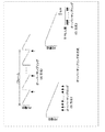
- FIG. 7 is an enlarged view of a portion surrounded by a circle A in FIG. 6, and is a diagram showing a specific example of a TCV arranged in the vicinity of a circuit block (vertical decoder in this example).
- FIG. 8 is a diagram showing a cross-sectional structure taken along the line AA ′ in FIG. In FIG. 7, only the wiring elements of the first chip (upper chip) 11 are shown.
- TCV 1 to TCV 5 are TCVs for supplying power, and connect the power supply line LPWR of power supplied from the second chip (lower chip) 12 to the circuit block CBLK of the first chip (upper chip) 11.
- TCV7 to TCV9 are TCVs for supplying control signals, and the control signal signal wiring LCS is connected between the upper and lower chips by TCV.
- the space between the power supply TCVs is wired in a wiring layer (not shown) different from the TCV connection wiring layer, and is connected to the circuit block CBLK.
- the signal wiring LCS is wired in the gap avoiding the columns of the TCVs 121 and 122.
- the TCV1 to TCV5 for supplying power are arranged more inside the edge of the chip than the TCV7 to 9 for supplying control signals.
- the area of the power supply line LPWR can be increased, and the resistance can be easily reduced.
- Each wiring is made of Al or Cu.
- the TCV junction CNT in the TCV junction CNT, as an example, the uppermost layer of the first chip (upper chip) 11 and the uppermost layer of the second chip (lower chip) 12 are connected.
- FIG. 8 shows an example of the TCV connection, and the usage of the wiring layers and the circuit positions in the upper and lower chips are arbitrary and are not limited.
- the impedance of the power wiring LPWR in the circuit block of the first chip (upper chip) 11 may increase in some cases. However, there is a risk of malfunction of the circuit block. If the power supply wiring width is simply increased, the chip size is increased. Therefore, the power supply wiring LPWR of the first chip (upper chip) 11 can be used for noise suppression and stability by using the wiring of the second chip (lower chip) 12. It is also possible to strengthen the supply.
- FIG. 9 is a diagram showing a modification of the circuit block wiring of FIG.
- FIG. 10 is a diagram showing a cross-sectional structure between BB ′ in FIG. In FIG. 10, for simplification, wiring necessary for connection in the logic circuit of the second chip (lower chip) 12 is not shown.
- the circuit block is divided into two circuit blocks CBLK1 and CBLK2, and a TCV is arranged in the space. Then, the second chip (lower chip) 12 is backed by the power supply line LPWRB wired in parallel with the power supply wiring LPWRU of the first chip (upper chip) 11.
- the connection between the upper and lower chips is made by TCV.
- the arrangement pitch is sufficiently small, and since it is processed in the wafer process, there is little possibility of causing a decrease in yield.
- a DC component such as a power source and a reference signal is supplied from the second chip (lower chip) 12 to the first chip (upper chip) 11 through the TCV, no special circuit is required for communication. As a result, the cost can be reduced.
- the signal at the edge that performs image data transmission / reception is, for example, an output signal of a comparator, so that the problem of noise at the TCV connection can be reduced, and the circuit configuration most suitable for circuit arrangement between the upper and lower chips Is possible. Focusing on analog characteristics and noise characteristics (especially 1 / f noise), by placing a circuit on which the noise affects the characteristics on the upper chip (first chip), the upper chip realizes characteristics with excellent noise resistance. be able to. Focusing on analog characteristics and noise characteristics (especially 1 / f noise), placing a circuit that affects noise on the upper chip (second chip), the lower chip uses a general-purpose ASIC (Logic) process It becomes possible to do.
- ASIC Application Specific integrated circuit
- the lower chip can be easily changed to the wafer FAB or expanded to another FAB. Costs can be reduced by using a minimum wiring layer for the upper chip, and problems associated with IR-drop (Drop) in the upper chip can be solved by reinforcing the lower chip wiring via the TCV.
- a chip cost reduction effect can be obtained by making the pixel portion and the logic portion of the image pickup device by an optimum process, performing wafer level bonding, and forming a laminated chip.
- the optimum process is a circuit having a necessary minimum number of wiring layers, in which the upper chip is composed of only high voltage transistors (HV.Tr), and the lower chip is a general-purpose ASIC process. By using the same upper chip and changing the lower chip, it is possible to develop various products.
- the vertical decoder 103 which is a digital circuit, is arranged on the first chip 11 in the configuration of FIG.
- other configurations can be employed.
- FIG. 11 is a block diagram illustrating a second configuration example of the solid-state imaging device according to the present embodiment.
- the solid-state imaging device 10B is configured such that the vertical decoder 103 is mounted on the second chip 12B side, and the analog circuit and the digital circuit are distributed to different chips. Is also possible.
- FIG. 12 is a block diagram illustrating a third configuration example of the solid-state imaging apparatus according to the present embodiment.
- FIG. 13 is a diagram illustrating an example of a floor plan of the first chip and the second chip in the solid-state imaging device of FIG.
- the scale of a circuit to be mounted on the second chip (lower chip) 12 is small, it is also possible to configure as shown in FIG. 12 in order to reduce the chip size of the solid-state imaging device. . That is, among the circuits mounted on the first chip (upper chip) 11 as in the solid-state imaging device 10C of FIG. 12, a part of the vertical drive circuit (row scanning circuit) 102 and the vertical decoder 103 is connected to the second chip ( It is also possible to move to (lower chip) 12. In this case, the vertical drive circuit (row scanning circuit) 102 may be divided into a first chip (upper chip) 11 and the vertical decoder 103 may be divided into a second chip (lower chip) 12.
- the vertical drive circuit (row scanning circuit) 102 and the vertical decoder 103 are integrated into one functional block, a part of which is mounted on the first chip (upper chip) 11 and the rest is the second chip (lower chip). ) 12 may be mounted.
- a circuit block in which the vertical driving circuit (row scanning circuit) 102 and the vertical decoder 103 are integrated is divided into upper and lower chips, thereby electrically connecting the divided blocks.
- a signal TCV area is added.
- the vertical drive circuit (row scanning circuit) 102 and the vertical decoder 103 are divided vertically, the layout width of the same block of the upper chip is reduced, and the chip size of the solid-state imaging device 10C is reduced.
- FIG. 14 is a block diagram illustrating a fourth configuration example of the solid-state imaging apparatus according to the present embodiment.
- FIG. 15 is a diagram illustrating an example of a floor plan of the first chip and the second chip in the solid-state imaging device of FIG.
- a configuration as shown in FIG. 14 may be used. That is, like the solid-state imaging device 10D of FIG. 14, all of the vertical drive circuit (row scanning circuit) 102 and the vertical decoder 103 and the reference signal supply unit 105 may be mounted on the second chip (lower chip) 12. Is possible. In this case, since the reference signal supply unit 105 includes an analog circuit, attention must be paid to the amount of noise in the second chip (lower chip) 12. However, the reference signal supply unit 105 is less susceptible to noise than the comparator 1041 and can be mounted on the second chip (lower chip) 12.
- the circuit scale of the image signal processing unit is reduced, but the vertical drive circuit (row scanning circuit) 102, the vertical decoder 103, and the reference signal supply unit 105 are included in the second chip (lower chip) 12. It is installed.
- the first chip (upper chip) 11 is reduced in chip size by eliminating all of the vertical drive circuit (row scanning circuit) 102 and the vertical decoder 103 and the reference signal supply unit 105.
- a part of the vertical drive circuit (row scanning circuit) 102 and the vertical decoder 103 can be mounted on the first chip (upper chip) 11.
- FIG. Are arranged in two rows on the left and right sides, but for the PAD arrangement, consideration is given to securing the PAD area and mounting on the lens module. Various aspects, such as placement, are possible.
- the column parallel ADC including the comparator 1041 and the counter circuit 1042 has been described as an example of the column processing unit 104.
- the present invention has a configuration of a column processing unit having another ADC function. Can be adopted.
- a configuration example of a column processing unit to which a ⁇ modulator ( ⁇ ADC) is applied will be described.
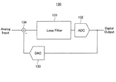
- FIG. 16 is a block diagram showing a basic configuration of the ⁇ ADC (AD) converter.
- the ⁇ ADC 130 includes a filter unit 131, an ADC (AD converter) 132 having a low resolution of 1 to 5 bits (bit), a DA converter (DAC) 133 having the same number of bits as the ADC, and a subtracter 134 in the input stage. Composed. Since the ⁇ ADC 130 is a system using feedback, non-linearity and noise of the circuit are compressed, and high resolution can be realized.
- ADC AD converter
- DAC DA converter
- the input circuit of the filter unit 131 and the DAC 133 are required to have high linearity and low noise.
- the nonlinearity of the DAC 133 increases the noise floor, it is important to ensure the linearity of the DAC when using an ADC other than one bit.
- FIG. 17 is a diagram showing a basic configuration of the peripheral portion of the pixel array in which ⁇ ADC is adopted as the column processing unit in the solid-state imaging device.
- the column processing unit 140 in FIG. 17 includes a column circuit 141 that performs processing such as CDS and a ⁇ modulator ( ⁇ ADC) 142 that performs ADC processing.
- ⁇ ADC ⁇ modulator
- an oversampling method is employed mainly for noise reduction.
- oversampling methods there are the following three methods as oversampling methods.
- 18A to 18C are diagrams for explaining the oversampling method.
- the first is a method of performing oversampling by performing high-speed reading during the video frame rate, as shown in FIG.
- the second is a method of performing oversampling within a frame by nondestructive readout as shown in FIG.
- a third method is adopted.
- ⁇ modulation output (ADC output) by oversampling is converted to a normal frame rate of N bits by a digital filter.
- FIG. 19 is a diagram illustrating a first configuration example of the peripheral portion of the pixel array in which a digital filter is employed in the column processing unit including the ⁇ ADC.
- FIG. 20 is a diagram illustrating a second configuration example of the peripheral portion of the pixel array in which a digital filter is employed for the column processing unit including the ⁇ ADC.
- the digital filter 143 is disposed on the output side of the ⁇ modulator 142, and the output control circuit 144 is disposed on the output side of the digital filter 143.
- an output control circuit 144 is disposed on the output side of the ⁇ modulator 142, and a digital filter 143 is disposed on the output side of the output control circuit 144.
- the digital filter 143 can be configured as a programmable filter by being realized by software.
- FIG. 21 is a block diagram illustrating a fifth configuration example of the solid-state imaging apparatus according to the present embodiment.
- the solid-state imaging device 10E of FIG. 21 shows a configuration example when the column processing units 140A and 140B of FIGS. 19 and 20 are employed.
- the edge portion that transmits and receives video data between the first chip 11 and the second chip 12 is an output of the ⁇ modulator that is a boundary circuit with a digital circuit among analog circuits.
- the column circuit 141 and the ⁇ modulator ( ⁇ ADC) 142 that performs ADC processing are arranged on the first chip 11E.
- a digital filter 143 and an output control circuit 144 are arranged on the second chip 12E side.
- FIG. 21 can be similarly applied to the same configurations as those of FIGS. 11, 12, and 14.
- the signal at the edge that transmits and receives image data is the output signal of the ⁇ modulator, which can reduce noise problems at the TCV connection, and is most suitable for circuit arrangement between the upper and lower chips.
- Circuit configuration is possible. Focusing on analog characteristics and noise characteristics (especially 1 / f noise), by placing a circuit on which the noise affects the characteristics on the upper chip (first chip), the upper chip realizes characteristics with excellent noise resistance. be able to. Focusing on analog characteristics and noise characteristics (especially 1 / f noise), placing a circuit that affects noise on the upper chip (second chip), the lower chip uses a general-purpose ASIC (Logic) process It becomes possible to do.
- the lower chip can be easily changed to the wafer FAB or expanded to another FAB. Costs can be reduced by using a minimum wiring layer for the upper chip, and problems associated with IR-drop (Drop) in the upper chip can be solved by reinforcing the lower chip wiring via the TCV.
- a chip cost reduction effect can be obtained by making the pixel portion and the logic portion of the image pickup device by an optimum process, performing wafer level bonding, and forming a laminated chip.
- the optimum process is a circuit having a necessary minimum number of wiring layers, in which the upper chip is composed of only high voltage transistors (HV.Tr), and the lower chip is a general-purpose ASIC process. By using the same upper chip and changing the lower chip, it is possible to develop various products.
- the configuration of the CMOS image sensor has been described as an example of the semiconductor device.
- the above configuration can be applied to, for example, a back-illuminated CMOS image sensor, and can exhibit the above-described effects. is there.
- the front irradiation type can sufficiently exhibit the above-described effects.
- the solid-state imaging device having such a configuration can be applied as an imaging device for a digital camera or a video camera.
- FIG. 22 is a diagram illustrating an example of a configuration of a camera system to which the solid-state imaging device according to the embodiment of the present invention is applied.
- the camera system 200 includes an imaging device 210 to which the CMOS image sensors (solid-state imaging devices) 10 and 10A to 10E according to the present embodiment can be applied. Furthermore, the camera system 200 includes an optical system that guides incident light (images a subject image) to the pixel area of the imaging device 210, for example, a lens 220 that forms incident light (image light) on the imaging surface.
- the camera system 200 includes a drive circuit (DRV) 230 that drives the imaging device 210 and a signal processing circuit (PRC) 240 that processes an output signal of the imaging device 210.
- DUV drive circuit
- PRC signal processing circuit
- the drive circuit 230 includes a timing generator (not shown) that generates various timing signals including a start pulse and a clock pulse that drive a circuit in the imaging device 210, and drives the imaging device 210 with a predetermined timing signal. .
- the signal processing circuit 240 performs predetermined signal processing on the output signal of the imaging device 210.
- the image signal processed by the signal processing circuit 240 is recorded on a recording medium such as a memory.
- the image information recorded on the recording medium is hard copied by a printer or the like. Further, the image signal processed by the signal processing circuit 240 is displayed as a moving image on a monitor including a liquid crystal display or the like.
- a high-precision camera can be realized by mounting the above-described imaging elements 10 and 10A to 10E as the imaging device 210 in an imaging apparatus such as a digital still camera.
- 10, 10A to 10E Solid-state imaging device (semiconductor device), 11: First chip (upper chip), 12: Second chip (lower chip), 101: Pixel array unit, 102 ⁇ Vertical drive circuit (row scanning circuit), 103 ⁇ Vertical decoder, 104 ⁇ Column processing unit, 1041 ⁇ Comparator, 1042 ⁇ Counter circuit, 105 ⁇ Reference signal supply unit, 106 ⁇ ..Horizontal scanning circuit (column scanning circuit) 107... Timing control circuit 108... Image signal processing unit 109... I / F system circuit, LPWR. Wiring, 120, 121, 122, 1-9 ... TCV, 130 ... ⁇ modulator ( ⁇ ADC), 140 ... column processing unit, 141 ... column circuit, 142 ... ⁇ modulator ( ⁇ ADC), 14 3 ... digital filter, 144 ... output control circuit unit, CBLK, CBLK1, CBLK2 ... circuit block, 200 ... camera system.
Landscapes
- Engineering & Computer Science (AREA)
- Physics & Mathematics (AREA)
- Power Engineering (AREA)
- Microelectronics & Electronic Packaging (AREA)
- Condensed Matter Physics & Semiconductors (AREA)
- General Physics & Mathematics (AREA)
- Computer Hardware Design (AREA)
- Electromagnetism (AREA)
- Signal Processing (AREA)
- Multimedia (AREA)
- Solid State Image Pick-Up Elements (AREA)
- Transforming Light Signals Into Electric Signals (AREA)
- Semiconductor Integrated Circuits (AREA)
Abstract
Description
もしくは、それぞれのチップをCOB(Chip On Board)実装している場合もある。
そこで、上記の2チップをチップレベルで組み立て、小型化と特性向上の両立を図る方法が提案されている(特許文献1,2参照)。
また、下チップから上チップへの電源やリファレンス信号などDC成分の供給において、1/fノイズ等の影響を受けやすい。そのため、上下チップ間の通信に特別な回路を必要とし、結果的にコスト増大を招くという不利益がある。
なお、説明は以下の順序で行う。
1.固体撮像装置の概要
2.プロセスフロー
3.回路配置
4.TCV(コンタクト用ビア、Through Contact Via)の配置
図1は、本発明の実施形態に係る半導体装置としての固体撮像装置の構成例を示す図である。
本実施形態においては、半導体装置の一例としてCMOSイメージセンサの構成について説明する。
この固体撮像装置10は、後で述べるように、ウェハレベルで貼り合わせ後、ダイシングで切り出した積層構造の撮像装置として形成される。
ボンディングパッドBPDおよび入出力回路は第2チップ(下チップ)12に形成されており、第1チップ(上チップ)には、第2チップ12にワイヤーボンドするための開口部OPNが形成されている。
映像データの上下チップ11,12間の信号授受を行う端縁部は、アナログ系回路のうちデジタル系回路との境界的な回路であるコンパレータやΣΔ変調器の出力部とする。
上下チップ11,12間の接続は、たとえばビアを通して行われる。
第1チップ(上チップ)11はCIS(CMOS Image Sensor)プロセスを用いる。ただし、トランジスタ(Tr.)は高耐圧トランジスタ(CMOS)のみ使用し、配線層数を画素アレイおよびその周辺回路の構成に必要な最低限の配線層数とし、コストの低減を図る。
ここで、高耐圧トランジスタとは、ゲート絶縁膜であるゲート酸化膜の厚さが、通常のMOS系トランジスタにより厚く設定されており、高い電圧において問題なく動作可能なトランジスタである。
なお、一般的なCISプロセスは、制御回路や画像処理回路など高速論理回路のために低耐圧LVの高速トランジスタTr.も高耐圧のトランジスタ(HV Tr.)と共に必要である。さらに高速論理回路のために、画素アレイおよび周辺回路に最低必要な配線層数より多い配線層数が必要となる。
第2チップ(下チップ)12は汎用ロジック(Logic)プロセスを用いて、FABの変更や展開を容易にする。
後で説明するように、本実施形態においては、画素アレイ、垂直デコータ、ドライバ、コンパレータ、およびDAC(Digital Analog converter)などが第1チップ11に搭載される。
高速論理回路、メモリ、インターフェース(I/F)回路など、低電圧で高速動作する回路を第2チップ(下チップ)12に搭載する。回路に要求される特性や規模を考慮してプロセス世代や配線層数を決定する。
同一の第1チップ(上チップ)11に対して、機能や特性、プロセスの異なる第2チップ(下チップ)12を組み合わせて製品展開を図る。
映像信号配線はコンパレータ回路の端部で、垂直信号線の配線ピッチで配置される。
制御信号ならびに電力供給用TCV(コンタクト用ビア、Through Contact Via)は主にチップ角部の4箇所に集中し、第1チップ(上チップ)11の信号配線領域を削減する。
第1チップ(上チップ)11の配線層数削減により、電源線抵抗が増加し、IR-Dropが増大する問題に対し、TCVを有効に配置することで、第2チップ(下チップ)12の配線を用いて第1チップ(上チップ)11の電源のノイズ対策や安定供給等のための強化を行う。
本実施形態において、図2の(A)のSOCの構成回路のうち、画素アレイと、アナログ回路で特に1/fノイズが回路特性に影響を及ぼす回路(コンパレータ、DAC回路など)を図2の(B)に示すチップ11に搭載する。
本実施形態では、上記の他に、高耐圧トランジスタ(HV Tr.)で構成される垂直デコーダ・ドライバ、パッド開口部OPNなどをひとつのチップにまとめたものが図2の(B)であり、図1の第1(上チップ)11に相当する。
なお、垂直デコーダ・ドライバおよびパッド開口部OPNについては必ずしも第1チップ(上チップ)に搭載する必要はなく、第2チップ(下チップ)に搭載される場合もある。
第1チップ(上チップ)11は高耐圧トランジスタ(CMOS)で構成され、画素特性を含め、アナログ特性とノイズ特性が十分に管理されたプロセスを用いており、ノイズ量は十分に低い。
また、配線層は第1チップ(上チップ)11を構成する回路に必要な最小限の配線層数で構成され、その数は、一般的にロジック(Logic)回路よりも少なくすることが可能である。
高耐圧トランジスタ(HV Tr.)だけを使用し、配線層数を削減することで、第1チップ(上チップ)11のプロセスコストはSOCタイプのCISのプロセスコストよりも安価にすることが可能となる。
低電圧高速Logicプロセスで構成可能な回路およびIO回路などがこれにあたる。
ロジック(Logic)チップは論理回路やメモリ回路用の低電圧高速トランジスタTr.と、入出力回路用の高耐圧トランジスタ(HV Tr.)が用いられている。低電圧高速トランジスタTr.とはゲート絶縁膜の膜厚を通常のMOS系トランジスタと同じあるいはそれ以下に設定して低電圧でも高速に動作するように形成されるトランジスタをいう。
FABの変更や展開を考慮して、一般的なASIC設計フローを用いて設計可能な回路構成とすることが望ましく、同一の上チップに対して、機能や特性、プロセスの異なる下チップを組み合わせて製品展開を図ることが容易になる。
一般的にロジック(Logic)プロセスの各種ノイズ、RTS、熱、たとえば1/fノイズ量は、ノイズ量を管理されたアナログプロセスより大きい。
ノイズ等の問題を解決しようとすれば、ロジック(Logic)プロセスのコスト上昇を招くだけでなく、Logic回路特性やその信頼性が劣化する可能性がある。このため、Logic FABの変更や展開を考慮すると、アナログ回路、特に1/fノイズが特性に影響する回路は第1チップ(上チップ)11に搭載する。
なお、低コストのロジック(Logic)を使うと1/fノイズは管理されていない、逆に管理されているプロセスは高コストになる。
図3の(A)~(C)は、本実施形態に係る積層構造の固体撮像装置のプロセスフローを示す図である。
第1チップ(上チップ)11側にパターニング後、第1チップ11側から第2チップ(下チップ)12の配線層までの貫通穴を開け、金属で埋めてビア(VIA)を形成する。本実施形態ではこのVIAをTCVと称する。
図3の(B)に示すように、このTCVにより上下チップ間の信号線および電源線が電気的に接合される。
そして、図3の(C)に示すように、第1チップ(上チップ)11側に、カラーフィルタおよびマイクロレンズの加工を行った後に、ダイシングによりチップとして切り出す。
次に、本実施形態に係る回路配置、すなわち、第1チップ(上チップ)11および第2チップ(下チップ)12それぞれに搭載する回路の分類について、図4に関連付けて説明する。
固体撮像装置10Aは、垂直駆動回路(行走査回路)102、垂直デコーダ103、カラム処理部104、参照信号供給部105、水平走査回路(列走査回路)106、タイミング制御回路107、および画像信号処理部108を含んで構成される。
固体撮像装置10Aは、さらにI/F系回路109を有する。
カラム処理部104は、コンパレータ1041およびカウンタ回路1042を含む。
また、画素アレイ部101の各単位画素を駆動制御する周辺の駆動系や、アナログ系、すなわち垂直駆動回路102、カラム処理部104のうちコンパレータ1041および参照信号供給部105などは画素アレイ部101と同一の第1チップ11上に集積される。
一方、タイミング制御回路107や画像信号処理部108、およびカラム処理部104のうち、カウンタ回路1042や水平走査回路106は上記とは別の第2チップ(半導体基板)12上に集積される。
図4において、図中の破線に囲まれた部分が第1チップ(上チップ)11、それ以外が第2チップ(下チップ)12に配置される。
単位画素は、転送トランジスタに加えてFD部の電位を制御するリセットトランジスタと、FD部の電位に応じた信号を出力する増幅トランジスタとを有する3トランジスタ構成のものを適用可能である。あるいは、単位画素は、さらに画素選択を行うための選択トランジスタを別に有する4トランジスタ構成のものなどを用いることができる。
行制御線の各一端は、垂直駆動回路102の各行に対応した各出力端に接続されている。垂直駆動回路102は、シフトレジスタなどによって構成され、行制御線を介して画素アレイ部101の行アドレスや行走査の制御を行う。
なお、ランプ波形の参照電圧Vrefを生成する手段としては、DACに限られるものではない。
DACは、タイミング制御回路107から与えられる制御信号による制御の下に、タイミング制御回路107から与えられるクロックに基づいてランプ波形の参照電圧Vrefを生成してカラム処理部104のADCに対して供給する。
高速フレームレートモードとは、通常フレームレートモード時に比べて、単位画素の露光時間を1/Nに設定してフレームレートをN倍、たとえば2倍に上げる動作モードである。
この動作モードの切り替えは、タイミング制御回路107から与えられる制御信号による制御によって実行される。また、タイミング制御回路107に対しては、外部のシステムコントローラ(図示せず)から、通常フレームレートモードと高速フレームレートモードの各動作モードとを切り替えるための指示情報が与えられる。
ADCは全て同じ構成となっており、コンパレータ1041、カウンタ回路1042である。たとえばアップ/ダウンカウンタ、転送スイッチおよびメモリ装置を有する。
コンパレータ1041は、たとえば参照電圧Vrefが信号電圧よりも大きいときに出力Vcoが“H”レベルになり、参照電圧Vrefが信号電圧Vx以下のときに出力Vcoが“L”レベルになる。
アップ/ダウンカウンタであるカウンタ回路1042は、非同期カウンタであり、タイミング制御回路107から与えられる制御信号による制御の下に、タイミング制御回路107からクロックがDACと同時に与えられる。
カウンタ回路1042は、このクロックに同期してダウン(DOWN)カウントまたはアップ(UP)カウントを行うことにより、比較器での比較動作の開始から比較動作の終了までの比較期間を計測する。
この水平走査回路106による制御の下に、ADCの各々でAD変換されたNビットのデジタル信号は順に水平信号線LHRに読み出され、この水平信号線LHRを経由して撮像データとして画像信号処理部108に出力される。
そして、その比較結果を、第2チップ(下チップ)12に搭載された、カウンタ回路1042により比較動作の開始から比較動作の終了までの比較期間を計測する。
ここで、上下のチップにそれぞれ搭載されたコンパレータ1041とカウンタ回路1042間にTCVが挿入され、これを通して信号転送が行われる、映像信号パスをこの部分で分離することが本実施形態の特徴の一つである。
コンパレータ1041は、画素アレイ部101および参照信号供給部105と同一チップ(上チップ)11に搭載され、アナログ特性およびノイズ特性(特に1/fノイズ)を十分な特性が得られるようにプロセスが管理される。
コンパレータ1041の出力は、たとえば参照電圧Vrefが信号電圧よりも大きいときに出力Vcoが“H”レベルになり、参照電圧Vrefが信号電圧Vx以下のときに出力Vcoが“L”レベルになるいわゆる時間軸にデータを持つCMOS論理信号である。
このCMOS論理信号は、ノイズ耐性が比較的高い。
TCVは主に、カラム処理部104のADC部の画像信号、第1チップ(上チップ)11に搭載された画素アレイ部101以外の回路の制御信号、および第1チップ(上チップ)11の電源/GNDを上下チップ間で接合するために用いられる。
制御信号および電力供給用のTCVは上記回路ブロックの短辺近傍に配置して、信号配線LSGおよび電源配線LPWRが、第1チップ(上チップ)11上を長く配線されることを避けることで、第1チップ(上チップ)11のチップ面積増加を防ぐ。
カラム処理部、画素信号用TCV120は、広帯域映像信号を第1チップと第2チップ間で接続するために、垂直信号線LSGNと同じピッチで直線状に、もしくは垂直信号線LSGNより大きいピッチでアレイ状に配置されたTCVのブロックである。第1チップ(上チップ)では、コンパレータ1041の回路ブロック、第2チップ(下チップ)では、カウンタ1042の回路ブロック、それぞれの長縁部に隣接して配置される。
ここで、第2チップ(下チップ)12において、十分に低いインピーダンスで供給すべき第1チップ(上チップ)11の回路ブロック近傍にあるTCVに接続される。
第1チップ(上チップ)11では、TCVから供給される電力の電源配線LPWRが各回路ブロックのポートPTUに直接接続される。
制御信号の信号配線LCSも同様に、たとえば第2チップ(下チップ)12のタイミング制御回路107から出力された制御信号の信号配線LCSは、接続すべき第1チップ(上チップ)11の回路ブロックの短縁部近傍のTCVに接続される。
そして、TCVを経由して第1チップ(上チップ)11の回路ブロックのポートPTUに入力される。
第1チップ(上チップ)11の回路ブロックは、図6の例では、垂直駆動回路102、垂直デコーダ103である。
図8は、図7のA-A’間の断面構造を示す図である。
なお、図7においては、第1チップ(上チップ)11の配線要素のみ記載されている。
図7において、TCV7~TCV9は制御信号供給用のTCVで、制御信号用信号配線LCSは上下チップ間をTCVで接続される。
第1チップ(上チップ)11では、電力供給用TCV間のスペースをTCV接続配線層とは図示しない別の配線層で配線され、回路ブロックCBLKに接続される。
この例では、TCV121,122の柱を避けてその間隙に信号配線LCSが配線されている。
そして、第1チップ(上チップ)11においては、電力供給用のTCV1~TCV5は、制御信号供給用のTCV7~9よりチップの縁部に対してより内側に配置されている。
これにより、図7に示すように、電源配線LPWRの面積を大きくすることが可能で、低抵抗化を実現しやすくなる。
各配線は、AlやCuにより形成される。
図8の例では、TCV接合部CNTにおいて、一例として、第1チップ(上チップ)11の最上位層と第2チップ(下チップ)12の最上位層を接続した場合を示している。
なお、図8はTCV接続の一例を示すもので、上下チップそれぞれにおける配線層の使い方や、回路の位置は任意であり、限定するものではない。
単純に電源配線幅を太くすればチップサイズの増加につながるため、第2チップ(下チップ)12の配線を用いて、第1チップ(上チップ)11の電源配線LPWRの電源のノイズ対策や安定供給等のための強化を行うことも可能である。
図10は、図9のB‐B’間の断面構造を示す図である。
なお、図10おいては、簡略化のため、第2チップ(下チップ)12のロジック回路内の接続に必要な配線は図示されていない。
そして、第2チップ(下チップ)12に、第1チップ(上チップ)11の電源配線LPWRUと平行して配線された電源線LPWRBによって裏打ちを行う。
また、第2チップ(下チップ)12から第1チップ(上チップ)11への電源やリファレンス信号などDC成分の供給も同TCVを介して行われるため、通信に特別な回路を必要とせず、結果的にコスト削減が可能となる。
画像データの信号授受を行う端縁部における信号は、たとえばコンパレータの出力信号とすることで、TCV接続部におけるノイズの問題を低減することができ、上下チップ間の回路配置にもっとも適した回路構成を可能とする。
アナログ特性とノイズ特性(特に1/fノイズ)に着目し、ノイズが特性に影響を及ぼす回路を上チップ(第1チップ)に配置することにより、上チップはノイズ耐性に優れた特性を実現することができる。
アナログ特性とノイズ特性(特に1/fノイズ)に着目し、ノイズが特性に影響を及ぼす回路を上チップ(第2チップ)に配置することにより、下チップは汎用のASIC(Logic)プロセスを使用することが可能となる。また、下チップについては、ウェハーFABの変更や、他FABへの展開が容易に可能となる。
上チップに最小限の配線層を用いてコスト削減を図ると共に、それに伴う上チップでのIR-ドロップ(Drop)などの問題を、TCVを介した下チップ配線で補強することにより解決できる。
撮像装置の画素部とロジック部をそれぞれ最適なプロセスで作りわけ、ウェハレベルの貼りあわせを行い、積層チップにすることで、チップコストの削減効果が得られる。
最適なプロセスとは、上チップは高電圧トランジスタ(HV.Tr)だけで構成される、必要最小限の配線層数を備えた回路であり、下チップは汎用のASICプロセスである。
同一の上チップを用いて、下チップを変更することで、多様な製品展開が可能となる。
図13は、図12の固体撮像装置における第1チップおよび第2チップのフロアプランの一例を示す図である。
すなわち、図12の固体撮像装置10Cのように、第1チップ(上チップ)11に搭載される回路のうち、垂直駆動回路(行走査回路)102、垂直デコーダ103の一部を第2チップ(下チップ)12に移動することも可能である。
この場合、垂直駆動回路(行走査回路)102を第1チップ(上チップ)11に、垂直デコーダ103を第2チップ(下チップ)12にと分割しても良い。
あるいは、垂直駆動回路(行走査回路)102と垂直デコーダ103を統合してひとつの機能ブロックとし、その一部を、第1チップ(上チップ)11に搭載し、残りを第2チップ(下チップ)12に搭載しても良い。
しかしながら、垂直駆動回路(行走査回路)102と垂直デコーダ103が上下に分割されたことにより、上チップの同ブロックのレイアウト幅が縮小され、固体撮像装置10Cのチップサイズが縮小される。
図15は、図14の固体撮像装置における第1チップおよび第2チップのフロアプランの一例を示す図である。
すなわち、図14の固体撮像装置10Dのように、垂直駆動回路(行走査回路)102、垂直デコーダ103の全てと、参照信号供給部105を、第2チップ(下チップ)12に搭載することも可能である。
この場合、参照信号供給部105には、アナログ回路が含まれるため、第2チップ(下チップ)12のノイズ量に注意が必要である。しかし、参照信号供給部105は、コンパレータ1041に比べ、ノイズの影響を受けにくいため、第2チップ(下チップ)12への搭載が可能である。
図5の構成例に比べ、第1チップ(上チップ)11は、垂直駆動回路(行走査回路)102、垂直デコーダ103の全てと、参照信号供給部105が削除されチップサイズが縮小されている。
また、図示はしないが、垂直駆動回路(行走査回路)102、垂直デコーダ103の一部を第1チップ(上チップ)11に搭載することも可能である
また、図15の例では、PAD配置を左右の2辺に2列配置しているが、PAD配置については、PAD領域の確保やレンズモジュールへの実装などを考慮しているもので、4辺配置、3辺配置、2辺2列配置など、種々の態様が可能である。
その一例として、ΣΔ変調器(ΣΔADC)を適用したカラム処理部の構成例について説明する。
図16は、ΣΔADC(AD)変換器の基本的な構成を示すブロック図である。
ΣΔADC130は、フィードバックを用いたシステムであるため、回路の非線形性、ノイズが圧縮され、高分解を実現することができる。
特に、DAC133の非線形性はノイズフロアを増加させる要因になるため、1ビット以外のADCを使用する場合は、DACの線形性を確保することが重要になる。
ΣΔ変調器142を採用する場合、ノイズ低減を主目的としてオーバーサンプリング方式が採用される。
図18の(A)~(C)は、オーバーサンプリングの方式を説明するための図である。
第1は、図18の(A)に示すように、ビデオフレームレート中に高速読み出しすることにより、オーバーサンプリングを行う方式である。
第2は、図18の(B)に示すように、非破壊読み出しによりフレーム内でオーバーサンプリングを行う方式である。
第3は、図18の(C)に示すように、サンプリングした一定値に対してオーバーサンプリングを行う方式である。
図17のカラム処理部140では、たとえば第3の方式が採用される。
図20は、ΣΔADCを含むカラム処理部にデジタルフィルタを採用した画素アレイ周辺部の第2の構成例を示す図である。
図20のカラム処理部140Bは、ΣΔ変調器142の出力側に出力制御回路144が配置され、出力制御回路144の出力側にデジタルフィルタ143が配置されている。
デジタルフィルタ143は、ソフトウェアで実現することにより、プログラマブルなフィルタが構成可能である。
この構成では、映像データの第1のチップ11と第2のチップ12間の信号授受を行う端縁部は、アナログ系回路のうちデジタル系回路との境界的な回路であるΣΔ変調器の出力部となっている。
すなわち、固体撮像装置10Eにおいては、第1のチップ11Eにカラム回路141およびADC処理を行うΣΔ変調器(ΣΔADC)142が配置される。そして、第2のチップ12E側にデジタルフィルタ143および出力制御回路144が配置される。
すなわち、画像データの信号授受を行う端縁部における信号は、ΣΔ変調器の出力信号とすることで、TCV接続部におけるノイズの問題を低減することができ、上下チップ間の回路配置にもっとも適した回路構成を可能とする。
アナログ特性とノイズ特性(特に1/fノイズ)に着目し、ノイズが特性に影響を及ぼす回路を上チップ(第1チップ)に配置することにより、上チップはノイズ耐性に優れた特性を実現することができる。
アナログ特性とノイズ特性(特に1/fノイズ)に着目し、ノイズが特性に影響を及ぼす回路を上チップ(第2チップ)に配置することにより、下チップは汎用のASIC(Logic)プロセスを使用することが可能となる。また、下チップについては、ウェハーFABの変更や、他FABへの展開が容易に可能となる。
上チップに最小限の配線層を用いてコスト削減を図ると共に、それに伴う上チップでのIR-ドロップ(Drop)などの問題を、TCVを介した下チップ配線で補強することにより解決できる。
撮像装置の画素部とロジック部をそれぞれ最適なプロセスで作りわけ、ウェハレベルの貼りあわせを行い、積層チップにすることで、チップコストの削減効果が得られる。
最適なプロセスとは、上チップは高電圧トランジスタ(HV.Tr)だけで構成される、必要最小限の配線層数を備えた回路であり、下チップは汎用のASICプロセスである。
同一の上チップを用いて、下チップを変更することで、多様な製品展開が可能となる。
このような構成を有する固体撮像素子は、デジタルカメラやビデオカメラの撮像デバイスとして適用することができる。
さらに、カメラシステム200は、この撮像デバイス210の画素領域に入射光を導く(被写体像を結像する)光学系、たとえば入射光(像光)を撮像面上に結像させるレンズ220を有する。
カメラシステム200は、撮像デバイス210を駆動する駆動回路(DRV)230と、撮像デバイス210の出力信号を処理する信号処理回路(PRC)240と、を有する。
信号処理回路240で処理された画像信号は、たとえばメモリなどの記録媒体に記録される。記録媒体に記録された画像情報は、プリンタなどによってハードコピーされる。また、信号処理回路240で処理された画像信号を液晶ディスプレイ等からなるモニターに動画として映し出される。
Claims (16)
- 第1チップと、
第2チップと、を有し、
上記第1チップと上記第2チップは貼り合わされた積層構造を有し、
上記第1チップは、
高耐圧トランジスタ系回路が搭載され、
上記第2チップは、
上記高耐圧トランジスタ系回路より低耐圧な低耐圧トランジスタ系回路が搭載され、
上記第1チップと上記第2チップ間の配線は、
上記第1チップに形成されたビアを通して接続される
半導体装置。 - 上記第1チップは、
アナログ系回路が搭載され、
上記第2チップは、
デジタル系回路が搭載される
請求項1記載の半導体装置。 - 上記第2チップには、
ボンディングパッドおよび入出力回路が配置され、
上記第1チップには、
上記第2チップにワイヤーボンディングするための開口部が形成されている
請求項1または2記載の半導体装置。 - 上記第1チップは、
搭載される回路ブロックの角部に電源および信号のポートを有するようにレイアウトされ、
信号および電力供給用のビアが上記回路ブロックの角部近傍に配置されている
請求項1から3のいずれか一に記載の半導体装置。 - 上記第1チップには、
電力供給用ビアと、
信号用ビアと、が形成され、
電力供給用ビアから供給される電力の電源配線が回路ブロックのポートに接続され、
信号配線は、第1チップの回路ブロックの角部近傍のビアに接続される
請求項4記載の半導体装置。 - 上記第1チップでは、
電力供給用ビア間のスペースを接続配線層とは別の配線層で配線され、回路ブロックに接続される
請求項4または5記載の半導体装置。 - 上記第1チップにおいては、電力供給用ビアは、信号供給用ビアよりチップの縁部に対してより内側に配置されている
請求項4から6のいずれか一に記載の半導体装置。 - 上記第2チップの配線を用いて、上記第1チップの電源配線が強化されている
請求項4から7のいずれか一に記載の半導体装置。 - 回路ブロックを複数に分割し、回路ブロック間のスペースに上記ビアが配置されている
請求項4から7のいずれか一に記載の半導体装置。 - 上記第2チップに、上記第1チップの電源配線と平行して配線された電源線によって裏打ちされている
請求項9記載の半導体装置。 - 光電変換を行う複数の画素が行列状に配列された画素部と、
上記画素部から複数の画素単位で画素信号の読み出しを行う画素信号読み出し回路と、を有し、
上記画素信号読み出し回路は、
画素の列配列に対応して配置され、読み出し信号電位と参照電圧とを比較判定し、その判定信号を出力する複数のコンパレータと、
上記比較器の出力により動作が制御され、対応する上記比較器の比較時間をカウントする複数のカウンタと、
第1チップと、
第2チップと、を有し、
上記第1チップと上記第2チップは貼り合わされた積層構造を有し、
上記第1チップは、
少なくとも上記画素部および上記画素信号読み出し回路のコンパレータが搭載され、
上記第2チップは、
少なくとも上記画素信号読み出し回路のカウンタが搭載され、
上記第1チップと上記第2チップ間の配線は、
上記第1チップに形成されたビアを通して接続される
固体撮像装置。 - 上記第1チップは、
アナログ系回路が搭載され、
上記第2チップは、
デジタル系回路が搭載される
請求項11記載の固体撮像装置。 - 上記第2チップには、
ボンディングパッドおよび入出力回路が配置され、
上記第1チップには、
上記画素部の周囲に上記第2チップにワイヤーボンディングするための開口部が形成されている
請求項11または12記載の固体撮像装置。 - 上記第1チップは、
搭載される回路ブロックの角部に電源および信号のポートを有するようにレイアウトされ、
信号および電力供給用のビアが上記回路ブロックの角部近傍に配置されている
請求項11から13記載の固体撮像装置。 - 上記第1チップには、
電力供給用ビアと、
信号用ビアと、が形成され、
電力供給用ビアから供給される電力の電源配線が回路ブロックのポートに接続され、
信号配線は、第1チップの回路ブロックの角部近傍のビアに接続される
請求項14記載の固体撮像装置。 - 固体撮像素子と、
上記撮像素子に被写体像を結像する光学系と、を有し、
上記固体撮像素子は、
光電変換を行う複数の画素が行列状に配列された画素部と、
上記画素部から複数の画素単位で画素信号の読み出しを行う画素信号読み出し回路と、を有し、
上記画素信号読み出し回路は、
画素の列配列に対応して配置され、読み出し信号電位と参照電圧とを比較判定し、その判定信号を出力する複数のコンパレータと、
上記比較器の出力により動作が制御され、対応する上記比較器の比較時間をカウントする複数のカウンタと、
第1チップと、
第2チップと、を有し、
上記第1チップと上記第2チップは貼り合わされた積層構造を有し、
上記第1チップは、
少なくとも上記画素部および上記画素信号読み出し回路のコンパレータが搭載され、
上記第2チップは、
少なくとも上記画素信号読み出し回路のカウンタが搭載され、
上記第1チップと上記第2チップ間の配線は、
上記第1チップに形成されたビアを通して接続される
カメラシステム。
Priority Applications (17)
| Application Number | Priority Date | Filing Date | Title |
|---|---|---|---|
| KR1020127016904A KR101774609B1 (ko) | 2010-01-08 | 2010-12-28 | 반도체 장치, 고체 촬상 장치, 및 카메라 시스템 |
| EP19159427.4A EP3528284A3 (en) | 2010-01-08 | 2010-12-28 | Semiconductor device, solid-state image sensor and camera system |
| CN201080065062.0A CN102782840B (zh) | 2010-01-08 | 2010-12-28 | 半导体器件、固态成像装置和相机系统 |
| EP17183032.6A EP3267480B1 (en) | 2010-01-08 | 2010-12-28 | Solid-state image sensor and camera system |
| EP19167097.5A EP3525237A1 (en) | 2010-01-08 | 2010-12-28 | Semiconductor device, solid-state image sensor and camera system |
| KR1020167024372A KR101775860B1 (ko) | 2010-01-08 | 2010-12-28 | 반도체 장치, 고체 촬상 장치, 및 카메라 시스템 |
| EP10842233.8A EP2528093B1 (en) | 2010-01-08 | 2010-12-28 | Solid-state imaging device and camera system |
| US13/519,450 US9093363B2 (en) | 2010-01-08 | 2010-12-28 | Semiconductor device, solid-state image sensor and camera system for reducing the influence of noise at a connection between chips |
| KR1020167024365A KR101774725B1 (ko) | 2010-01-08 | 2010-12-28 | 반도체 장치, 고체 촬상 장치, 및 카메라 시스템 |
| US14/742,178 US9641777B2 (en) | 2010-01-08 | 2015-06-17 | Semiconductor device, solid-state image sensor and camera system |
| US15/176,602 US9565383B2 (en) | 2010-01-08 | 2016-06-08 | Semiconductor device, solid-state image sensor and camera system |
| US15/273,565 US9634052B2 (en) | 2010-01-08 | 2016-09-22 | Semiconductor device, solid-state image sensor and camera system |
| US15/448,869 US9762835B2 (en) | 2010-01-08 | 2017-03-03 | Semiconductor device, solid-state image sensor and camera system |
| US15/668,265 US9954024B2 (en) | 2010-01-08 | 2017-08-03 | Semiconductor device, solid-state image sensor and camera system |
| US15/832,951 US10319773B2 (en) | 2010-01-08 | 2017-12-06 | Semiconductor device, solid-state image sensor and camera system |
| US16/226,144 US10396115B2 (en) | 2010-01-08 | 2018-12-19 | Semiconductor device, solid-state image sensor and camera system |
| US16/514,393 US10615211B2 (en) | 2010-01-08 | 2019-07-17 | Semiconductor device, solid-state image sensor and camera system |
Applications Claiming Priority (4)
| Application Number | Priority Date | Filing Date | Title |
|---|---|---|---|
| JP2010002979 | 2010-01-08 | ||
| JP2010-002979 | 2010-01-08 | ||
| JP2010255934A JP5685898B2 (ja) | 2010-01-08 | 2010-11-16 | 半導体装置、固体撮像装置、およびカメラシステム |
| JP2010-255934 | 2010-11-16 |
Related Child Applications (2)
| Application Number | Title | Priority Date | Filing Date |
|---|---|---|---|
| US13/519,450 A-371-Of-International US9093363B2 (en) | 2010-01-08 | 2010-12-28 | Semiconductor device, solid-state image sensor and camera system for reducing the influence of noise at a connection between chips |
| US14/742,178 Continuation US9641777B2 (en) | 2010-01-08 | 2015-06-17 | Semiconductor device, solid-state image sensor and camera system |
Publications (1)
| Publication Number | Publication Date |
|---|---|
| WO2011083722A1 true WO2011083722A1 (ja) | 2011-07-14 |
Family
ID=44306407
Family Applications (1)
| Application Number | Title | Priority Date | Filing Date |
|---|---|---|---|
| PCT/JP2010/073671 WO2011083722A1 (ja) | 2010-01-08 | 2010-12-28 | 半導体装置、固体撮像装置、およびカメラシステム |
Country Status (8)
| Country | Link |
|---|---|
| US (9) | US9093363B2 (ja) |
| EP (4) | EP3525237A1 (ja) |
| JP (1) | JP5685898B2 (ja) |
| KR (3) | KR101774725B1 (ja) |
| CN (1) | CN102782840B (ja) |
| DE (2) | DE202010018542U1 (ja) |
| TW (1) | TWI456731B (ja) |
| WO (1) | WO2011083722A1 (ja) |
Cited By (26)
| Publication number | Priority date | Publication date | Assignee | Title |
|---|---|---|---|---|
| JP2013051674A (ja) * | 2011-08-02 | 2013-03-14 | Canon Inc | 周辺回路を配置しチップ面積増大を抑制した撮像素子及び撮像装置 |
| WO2013057903A1 (ja) * | 2011-10-21 | 2013-04-25 | ソニー株式会社 | 半導体装置、固体撮像装置、およびカメラシステム |
| US20140077063A1 (en) * | 2012-09-20 | 2014-03-20 | Aptina Imaging Corporation | Imagers with stacked integrated circuit dies |
| WO2015159728A1 (ja) * | 2014-04-15 | 2015-10-22 | ソニー株式会社 | 撮像素子、電子機器 |
| JP2016530701A (ja) * | 2013-06-13 | 2016-09-29 | ビーエーエスエフ ソシエタス・ヨーロピアBasf Se | 光学検出器及び当該光学検出器の製造方法 |
| WO2017077620A1 (ja) * | 2015-11-05 | 2017-05-11 | オリンパス株式会社 | 固体撮像装置 |
| US9748291B2 (en) | 2014-09-26 | 2017-08-29 | Semiconductor Energy Laboratory Co., Ltd. | Imaging device having a third circuit with a region overlapping with a fourth circuit |
| US9989623B2 (en) | 2013-06-13 | 2018-06-05 | Basf Se | Detector for determining a longitudinal coordinate of an object via an intensity distribution of illuminated pixels |
| JP2018102002A (ja) * | 2011-08-02 | 2018-06-28 | キヤノン株式会社 | 撮像素子及び撮像装置 |
| US10012532B2 (en) | 2013-08-19 | 2018-07-03 | Basf Se | Optical detector |
| US10094927B2 (en) | 2014-09-29 | 2018-10-09 | Basf Se | Detector for optically determining a position of at least one object |
| US10120078B2 (en) | 2012-12-19 | 2018-11-06 | Basf Se | Detector having a transversal optical sensor and a longitudinal optical sensor |
| US10353049B2 (en) | 2013-06-13 | 2019-07-16 | Basf Se | Detector for optically detecting an orientation of at least one object |
| US10412283B2 (en) | 2015-09-14 | 2019-09-10 | Trinamix Gmbh | Dual aperture 3D camera and method using differing aperture areas |
| TWI701493B (zh) * | 2016-03-15 | 2020-08-11 | 大陸商寧波舜宇光電信息有限公司 | 一體基座組件、基於一體封裝工藝的攝像模組和陣列攝像模組 |
| US10775505B2 (en) | 2015-01-30 | 2020-09-15 | Trinamix Gmbh | Detector for an optical detection of at least one object |
| US10890491B2 (en) | 2016-10-25 | 2021-01-12 | Trinamix Gmbh | Optical detector for an optical detection |
| US10948567B2 (en) | 2016-11-17 | 2021-03-16 | Trinamix Gmbh | Detector for optically detecting at least one object |
| US10955936B2 (en) | 2015-07-17 | 2021-03-23 | Trinamix Gmbh | Detector for optically detecting at least one object |
| US11041718B2 (en) | 2014-07-08 | 2021-06-22 | Basf Se | Detector for determining a position of at least one object |
| US11060922B2 (en) | 2017-04-20 | 2021-07-13 | Trinamix Gmbh | Optical detector |
| US11067692B2 (en) | 2017-06-26 | 2021-07-20 | Trinamix Gmbh | Detector for determining a position of at least one object |
| US11125880B2 (en) | 2014-12-09 | 2021-09-21 | Basf Se | Optical detector |
| US11211513B2 (en) | 2016-07-29 | 2021-12-28 | Trinamix Gmbh | Optical sensor and detector for an optical detection |
| US11428787B2 (en) | 2016-10-25 | 2022-08-30 | Trinamix Gmbh | Detector for an optical detection of at least one object |
| US11860292B2 (en) | 2016-11-17 | 2024-01-02 | Trinamix Gmbh | Detector and methods for authenticating at least one object |
Families Citing this family (82)
| Publication number | Priority date | Publication date | Assignee | Title |
|---|---|---|---|---|
| JP5820979B2 (ja) * | 2008-12-26 | 2015-11-24 | パナソニックIpマネジメント株式会社 | 固体撮像デバイス |
| JP5685898B2 (ja) | 2010-01-08 | 2015-03-18 | ソニー株式会社 | 半導体装置、固体撮像装置、およびカメラシステム |
| JP5843475B2 (ja) * | 2010-06-30 | 2016-01-13 | キヤノン株式会社 | 固体撮像装置および固体撮像装置の製造方法 |
| JP6173410B2 (ja) * | 2010-06-30 | 2017-08-02 | キヤノン株式会社 | 固体撮像装置および固体撮像装置の製造方法 |
| US8890047B2 (en) * | 2011-09-21 | 2014-11-18 | Aptina Imaging Corporation | Stacked-chip imaging systems |
| JP5645786B2 (ja) * | 2011-09-22 | 2014-12-24 | 富士フイルム株式会社 | 固体撮像装置及びカメラモジュール |
| JP2013090305A (ja) | 2011-10-21 | 2013-05-13 | Sony Corp | 比較器、ad変換器、固体撮像装置、およびカメラシステム |
| JP5923929B2 (ja) * | 2011-10-27 | 2016-05-25 | ソニー株式会社 | 固体撮像素子およびカメラシステム |
| JP2014241458A (ja) * | 2011-10-28 | 2014-12-25 | ソニー株式会社 | 固体撮像素子およびカメラシステム |
| JP6214132B2 (ja) | 2012-02-29 | 2017-10-18 | キヤノン株式会社 | 光電変換装置、撮像システムおよび光電変換装置の製造方法 |
| JP6016378B2 (ja) | 2012-02-29 | 2016-10-26 | キヤノン株式会社 | 光電変換装置、および光電変換装置を用いた撮像システム |
| US9607971B2 (en) | 2012-06-04 | 2017-03-28 | Sony Corporation | Semiconductor device and sensing system |
| TWI583195B (zh) | 2012-07-06 | 2017-05-11 | 新力股份有限公司 | A solid-state imaging device and a solid-state imaging device, and an electronic device |
| US8710607B2 (en) | 2012-07-12 | 2014-04-29 | Taiwan Semiconductor Manufacturing Company, Ltd. | Method and apparatus for image sensor packaging |
| JP6128787B2 (ja) | 2012-09-28 | 2017-05-17 | キヤノン株式会社 | 半導体装置 |
| JP6037878B2 (ja) * | 2013-02-13 | 2016-12-07 | オリンパス株式会社 | 撮像装置 |
| US8946784B2 (en) * | 2013-02-18 | 2015-02-03 | Taiwan Semiconductor Manufacturing Company, Ltd. | Method and apparatus for image sensor packaging |
| JP2014165396A (ja) * | 2013-02-26 | 2014-09-08 | Sony Corp | 固体撮像装置および電子機器 |
| CN111314632B (zh) * | 2013-03-14 | 2023-04-21 | 株式会社尼康 | 摄像单元及摄像装置 |
| JP6190184B2 (ja) * | 2013-06-28 | 2017-08-30 | キヤノン株式会社 | 撮像素子、撮像装置、その制御方法、および制御プログラム |
| TWI659652B (zh) | 2013-08-05 | 2019-05-11 | 新力股份有限公司 | 攝像裝置、電子機器 |
| TWI631854B (zh) * | 2013-08-05 | 2018-08-01 | 日商新力股份有限公司 | Conversion device, imaging device, electronic device, conversion method |
| JP6192469B2 (ja) * | 2013-10-01 | 2017-09-06 | オリンパス株式会社 | 撮像装置 |
| JP6346740B2 (ja) * | 2013-10-08 | 2018-06-20 | オリンパス株式会社 | 撮像装置 |
| JP6463944B2 (ja) | 2013-11-25 | 2019-02-06 | キヤノン株式会社 | 撮像素子、撮像装置及び携帯電話機 |
| JP6458114B2 (ja) * | 2013-11-29 | 2019-01-23 | キヤノン株式会社 | 撮像素子、撮像装置及び携帯電話機 |
| JP6320272B2 (ja) * | 2013-11-29 | 2018-05-09 | キヤノン株式会社 | 撮像素子、撮像装置及び携帯電話機 |
| JP6278881B2 (ja) | 2013-12-06 | 2018-02-14 | キヤノン株式会社 | 撮像素子、撮像装置及び携帯電話機 |
| JP6314477B2 (ja) * | 2013-12-26 | 2018-04-25 | ソニー株式会社 | 電子デバイス |
| US9536920B2 (en) * | 2014-03-28 | 2017-01-03 | Taiwan Semiconductor Manufacturing Company, Ltd. | Stacked image sensor having a barrier layer |
| JP2015195235A (ja) * | 2014-03-31 | 2015-11-05 | ソニー株式会社 | 固体撮像素子、電子機器、および撮像方法 |
| US20150296158A1 (en) * | 2014-04-10 | 2015-10-15 | Forza Silicon Corporation | Reconfigurable CMOS Image Sensor |
| US9794499B2 (en) * | 2014-04-29 | 2017-10-17 | Fermi Research Alliance, Llc | Wafer-scale pixelated detector system |
| US10084983B2 (en) | 2014-04-29 | 2018-09-25 | Fermi Research Alliance, Llc | Wafer-scale pixelated detector system |
| CN104092963B (zh) * | 2014-06-24 | 2018-01-02 | 上海集成电路研发中心有限公司 | 一种可重构的cmos图像传感器芯片及其形成方法 |
| US9531959B2 (en) * | 2014-08-29 | 2016-12-27 | Semiconductor Components Industries, Llc | Imaging systems and methods for capturing image data at high scan rates |
| JP6930556B2 (ja) * | 2014-09-30 | 2021-09-01 | 株式会社ニコン | 撮像素子および撮像装置 |
| US10070088B2 (en) | 2015-01-05 | 2018-09-04 | Canon Kabushiki Kaisha | Image sensor and image capturing apparatus for simultaneously performing focus detection and image generation |
| JP6218799B2 (ja) | 2015-01-05 | 2017-10-25 | キヤノン株式会社 | 撮像素子及び撮像装置 |
| US10389961B2 (en) | 2015-04-09 | 2019-08-20 | Semiconductor Energy Laboratory Co., Ltd. | Imaging device and electronic device |
| EP3288081B1 (en) | 2015-04-24 | 2022-07-27 | Sony Group Corporation | Solid state image sensor and electronic device comprising the same |
| TWI692859B (zh) | 2015-05-15 | 2020-05-01 | 日商新力股份有限公司 | 固體攝像裝置及其製造方法、以及電子機器 |
| JP6272387B2 (ja) | 2015-05-29 | 2018-01-31 | キヤノン株式会社 | 撮像素子および撮像装置 |
| JP6608185B2 (ja) * | 2015-06-18 | 2019-11-20 | キヤノン株式会社 | 積層型イメージセンサおよび撮像装置 |
| KR102422224B1 (ko) | 2015-07-31 | 2022-07-18 | 삼성전자주식회사 | 적층형 이미지 센서 및 이를 포함하는 시스템 |
| WO2017038403A1 (ja) | 2015-09-01 | 2017-03-09 | ソニー株式会社 | 積層体 |
| US11297258B2 (en) * | 2015-10-01 | 2022-04-05 | Qualcomm Incorporated | High dynamic range solid state image sensor and camera system |
| US10879298B2 (en) | 2016-03-24 | 2020-12-29 | Nikon Corporation | Image sensor and image capturing device |
| JPWO2018012143A1 (ja) | 2016-07-11 | 2019-04-25 | ソニーセミコンダクタソリューションズ株式会社 | 撮像素子および撮像装置 |
| JP2018042139A (ja) * | 2016-09-08 | 2018-03-15 | ソニーセミコンダクタソリューションズ株式会社 | 撮像素子および撮像素子の動作方法、撮像装置、および電子機器 |
| EP3570325B1 (en) * | 2017-01-12 | 2020-10-28 | Mitsubishi Electric Corporation | Infrared sensor substrate and infrared sensor device |
| EP4235793A3 (en) * | 2017-06-29 | 2023-10-04 | Sony Semiconductor Solutions Corporation | Wafer bonded back illuminated imager |
| JP7102119B2 (ja) | 2017-09-29 | 2022-07-19 | キヤノン株式会社 | 半導体装置および機器 |
| TW202315106A (zh) * | 2017-10-30 | 2023-04-01 | 日商索尼半導體解決方案公司 | 固體攝像裝置及電子機器 |
| US10529757B2 (en) | 2017-12-15 | 2020-01-07 | Atomera Incorporated | CMOS image sensor including pixels with read circuitry having a superlattice |
| US10608027B2 (en) * | 2017-12-15 | 2020-03-31 | Atomera Incorporated | Method for making CMOS image sensor including stacked semiconductor chips and image processing circuitry including a superlattice |
| US10615209B2 (en) | 2017-12-15 | 2020-04-07 | Atomera Incorporated | CMOS image sensor including stacked semiconductor chips and readout circuitry including a superlattice |
| US10367028B2 (en) | 2017-12-15 | 2019-07-30 | Atomera Incorporated | CMOS image sensor including stacked semiconductor chips and image processing circuitry including a superlattice |
| US10608043B2 (en) * | 2017-12-15 | 2020-03-31 | Atomera Incorporation | Method for making CMOS image sensor including stacked semiconductor chips and readout circuitry including a superlattice |
| US10529768B2 (en) | 2017-12-15 | 2020-01-07 | Atomera Incorporated | Method for making CMOS image sensor including pixels with read circuitry having a superlattice |
| US10708529B2 (en) * | 2017-12-20 | 2020-07-07 | Semiconductor Components Industries, Llc | Image sensors with low-voltage transistors |
| CN108281412B (zh) * | 2018-01-23 | 2020-02-14 | 德淮半导体有限公司 | 堆叠式图像传感器、像素管芯及其制造方法 |
| JP7080660B2 (ja) * | 2018-02-09 | 2022-06-06 | キヤノン株式会社 | 光電変換装置、撮像システム、および、移動体 |
| JP2019140237A (ja) * | 2018-02-09 | 2019-08-22 | キヤノン株式会社 | 光電変換装置および撮像システム |
| JP6575635B2 (ja) * | 2018-04-26 | 2019-09-18 | ソニー株式会社 | 半導体装置、固体撮像装置、およびカメラシステム |
| US10530380B2 (en) * | 2018-04-27 | 2020-01-07 | Raytheon Company | Massively parallel three dimensional per pixel single slope analog to digital converter |
| JP6669196B2 (ja) * | 2018-05-28 | 2020-03-18 | 株式会社ニコン | 撮像素子及び撮像装置 |
| JP6708698B2 (ja) * | 2018-05-31 | 2020-06-10 | キヤノン株式会社 | 光電変換装置、および光電変換装置を用いた撮像システム |
| WO2020027233A1 (ja) * | 2018-07-31 | 2020-02-06 | ソニーセミコンダクタソリューションズ株式会社 | 撮像装置及び車両制御システム |
| EP3833007B1 (en) * | 2018-07-31 | 2024-03-13 | Sony Semiconductor Solutions Corporation | Layered-type light-receiving sensor and electronic device |
| JP7327916B2 (ja) * | 2018-09-11 | 2023-08-16 | キヤノン株式会社 | 光電変換装置および機器 |
| JP7402606B2 (ja) * | 2018-10-31 | 2023-12-21 | ソニーセミコンダクタソリューションズ株式会社 | 固体撮像装置及び電子機器 |
| CN113228230A (zh) * | 2018-12-20 | 2021-08-06 | 索尼半导体解决方案公司 | 摄像装置 |
| US20220086379A1 (en) * | 2019-01-25 | 2022-03-17 | Sony Semiconductor Solutions Corporation | Image capturing device and electronic apparatus |
| TWI692857B (zh) * | 2019-01-25 | 2020-05-01 | 世界先進積體電路股份有限公司 | 半導體裝置與生物辨識裝置 |
| CN109923858B (zh) * | 2019-01-31 | 2021-08-13 | 深圳市汇顶科技股份有限公司 | 图像传感器及其制造方法和电子设备 |
| KR20200110020A (ko) | 2019-03-15 | 2020-09-23 | 삼성전자주식회사 | 디스플레이 드라이버 ic 소자 |
| JP6957559B2 (ja) | 2019-06-24 | 2021-11-02 | キヤノン株式会社 | 半導体装置および機器 |
| JP7279746B2 (ja) * | 2019-06-27 | 2023-05-23 | 株式会社ニコン | 撮像ユニットおよび撮像装置 |
| JP2020096367A (ja) * | 2020-02-27 | 2020-06-18 | 株式会社ニコン | 画像処理装置および撮像装置 |
| JP7171649B2 (ja) | 2020-05-15 | 2022-11-15 | キヤノン株式会社 | 撮像装置および撮像システム |
| JP2022158017A (ja) * | 2021-04-01 | 2022-10-14 | キヤノン株式会社 | 信号処理装置 |
Citations (7)
| Publication number | Priority date | Publication date | Assignee | Title |
|---|---|---|---|---|
| JP2000032350A (ja) * | 1998-04-29 | 2000-01-28 | Texas Instr Inc <Ti> | 画素毎のa/d変換器を備えるcmos撮像装置 |
| JP2001339057A (ja) * | 2000-05-30 | 2001-12-07 | Mitsumasa Koyanagi | 3次元画像処理装置の製造方法 |
| JP2004146816A (ja) * | 2002-09-30 | 2004-05-20 | Matsushita Electric Ind Co Ltd | 固体撮像装置およびこれを用いた機器 |
| JP2008172609A (ja) * | 2007-01-12 | 2008-07-24 | Sony Corp | 固体撮像装置、撮像装置 |
| JP2009164478A (ja) * | 2008-01-09 | 2009-07-23 | Hitachi Ltd | 半導体装置 |
| JP2009177436A (ja) * | 2008-01-23 | 2009-08-06 | Sharp Corp | 固体撮像装置、信号処理装置、および電子情報機器 |
| JP2009212162A (ja) * | 2008-02-29 | 2009-09-17 | Fujifilm Corp | 放射線検出器 |
Family Cites Families (58)
| Publication number | Priority date | Publication date | Assignee | Title |
|---|---|---|---|---|
| JP3432963B2 (ja) * | 1995-06-15 | 2003-08-04 | 沖電気工業株式会社 | 半導体集積回路 |
| US7129985B1 (en) * | 1998-11-24 | 2006-10-31 | Canon Kabushiki Kaisha | Image sensing apparatus arranged on a single substrate |
| AU2003900746A0 (en) * | 2003-02-17 | 2003-03-06 | Silverbrook Research Pty Ltd | Methods, systems and apparatus (NPS041) |
| JP3737333B2 (ja) * | 2000-03-17 | 2006-01-18 | 沖電気工業株式会社 | 半導体装置 |
| JP2001289886A (ja) * | 2000-04-03 | 2001-10-19 | Sanyo Electric Co Ltd | 電池電圧測定装置 |
| US6809769B1 (en) * | 2000-06-22 | 2004-10-26 | Pixim, Inc. | Designs of digital pixel sensors |
| US7139024B2 (en) * | 2002-07-26 | 2006-11-21 | Xerox Corporation | Large-area imager with direct digital pixel output |
| JP3652676B2 (ja) * | 2002-09-17 | 2005-05-25 | 松下電器産業株式会社 | 撮像装置および画像ピックアップシステム |
| CN1234234C (zh) * | 2002-09-30 | 2005-12-28 | 松下电器产业株式会社 | 固体摄像器件及使用该固体摄像器件的设备 |
| JP4414646B2 (ja) * | 2002-11-18 | 2010-02-10 | 浜松ホトニクス株式会社 | 光検出装置 |
| KR100494474B1 (ko) * | 2003-01-14 | 2005-06-10 | 삼성전기주식회사 | 카메라 모듈 및 그 제조방법 |
| KR100568223B1 (ko) * | 2003-06-18 | 2006-04-07 | 삼성전자주식회사 | 고체 촬상용 반도체 장치 |
| US6927432B2 (en) * | 2003-08-13 | 2005-08-09 | Motorola, Inc. | Vertically integrated photosensor for CMOS imagers |
| JP4068616B2 (ja) | 2003-12-26 | 2008-03-26 | エルピーダメモリ株式会社 | 半導体装置 |
| US7009287B2 (en) * | 2004-03-01 | 2006-03-07 | United Microelectronics Corp. | Chip on photosensitive device package structure and electrical connection thereof |
| US7528473B2 (en) * | 2004-03-19 | 2009-05-05 | Renesas Technology Corp. | Electronic circuit, a semiconductor device and a mounting substrate |
| US7268369B2 (en) * | 2004-07-06 | 2007-09-11 | Fujifilm Corporation | Functional device and method for producing the same |
| JP3979405B2 (ja) * | 2004-07-13 | 2007-09-19 | セイコーエプソン株式会社 | 電気光学装置、実装構造体及び電子機器 |
| JP4816457B2 (ja) | 2004-09-02 | 2011-11-16 | ソニー株式会社 | 撮像装置及び撮像結果の出力方法 |
| JP4379295B2 (ja) | 2004-10-26 | 2009-12-09 | ソニー株式会社 | 半導体イメージセンサー・モジュール及びその製造方法 |
| US8368096B2 (en) * | 2005-01-04 | 2013-02-05 | Aac Technologies Japan R&D Center Co., Ltd. | Solid state image pick-up device and method for manufacturing the same with increased structural integrity |
| US20060186315A1 (en) * | 2005-02-22 | 2006-08-24 | Kany-Bok Lee | Active pixel image sensors |
| JP4748648B2 (ja) | 2005-03-31 | 2011-08-17 | ルネサスエレクトロニクス株式会社 | 半導体装置 |
| KR101070913B1 (ko) | 2005-05-19 | 2011-10-06 | 삼성테크윈 주식회사 | 반도체 칩 적층 패키지 |
| TW201101476A (en) * | 2005-06-02 | 2011-01-01 | Sony Corp | Semiconductor image sensor module and method of manufacturing the same |
| JP5194382B2 (ja) * | 2005-08-18 | 2013-05-08 | セイコーエプソン株式会社 | 電気光学装置及び電子機器 |
| JP2007228460A (ja) | 2006-02-27 | 2007-09-06 | Mitsumasa Koyanagi | 集積センサを搭載した積層型半導体装置 |
| US20080308914A1 (en) * | 2006-03-17 | 2008-12-18 | Chipmos Technologies Inc. | Chip package |
| US7902654B2 (en) * | 2006-05-10 | 2011-03-08 | Qualcomm Incorporated | System and method of silicon switched power delivery using a package |
| JP4289377B2 (ja) * | 2006-08-21 | 2009-07-01 | ソニー株式会社 | 物理量検出装置及び撮像装置 |
| JP2008053286A (ja) * | 2006-08-22 | 2008-03-06 | Matsushita Electric Ind Co Ltd | 撮像装置チップセット及び画像ピックアップシステム |
| WO2008039543A1 (en) * | 2006-09-27 | 2008-04-03 | University Of Connecticut | Implantable biosensor and methods of use thereof |
| JP2008085755A (ja) | 2006-09-28 | 2008-04-10 | Toshiba Corp | 画像撮像装置 |
| US8049256B2 (en) | 2006-10-05 | 2011-11-01 | Omnivision Technologies, Inc. | Active pixel sensor having a sensor wafer connected to a support circuit wafer |
| JP2008235478A (ja) | 2007-03-19 | 2008-10-02 | Nikon Corp | 撮像素子 |
| US7488928B2 (en) * | 2007-04-20 | 2009-02-10 | Alexander Krymski | Image sensor circuits and methods with multiple readout lines per column of pixel circuits |
| JP4337906B2 (ja) * | 2007-05-10 | 2009-09-30 | ソニー株式会社 | 固体撮像素子およびカメラシステム |
| JP2009038142A (ja) * | 2007-07-31 | 2009-02-19 | Elpida Memory Inc | 半導体積層パッケージ |
| JP4940064B2 (ja) * | 2007-08-28 | 2012-05-30 | ルネサスエレクトロニクス株式会社 | 半導体装置 |
| US8415783B1 (en) * | 2007-10-04 | 2013-04-09 | Xilinx, Inc. | Apparatus and methodology for testing stacked die |
| US8564676B2 (en) * | 2007-11-28 | 2013-10-22 | Sanyo Semiconductor Co., Ltd. | Semiconductor device with anti-shake control function |
| KR101435522B1 (ko) * | 2008-01-23 | 2014-09-02 | 삼성전자 주식회사 | 바이오 칩 |
| US8183510B2 (en) * | 2008-02-12 | 2012-05-22 | Omnivision Technologies, Inc. | Image sensor with buried self aligned focusing element |
| JP5125632B2 (ja) * | 2008-03-10 | 2013-01-23 | セイコーエプソン株式会社 | 実装構造体および電気光学装置 |
| JP4538058B2 (ja) * | 2008-03-28 | 2010-09-08 | 株式会社東芝 | 集積半導体装置及び集積3次元半導体装置 |
| US8354742B2 (en) * | 2008-03-31 | 2013-01-15 | Stats Chippac, Ltd. | Method and apparatus for a package having multiple stacked die |
| US8362617B2 (en) * | 2008-05-01 | 2013-01-29 | Infineon Technologies Ag | Semiconductor device |
| JP4799594B2 (ja) * | 2008-08-19 | 2011-10-26 | 株式会社東芝 | 固体撮像装置およびその製造方法 |
| US7795650B2 (en) * | 2008-12-09 | 2010-09-14 | Teledyne Scientific & Imaging Llc | Method and apparatus for backside illuminated image sensors using capacitively coupled readout integrated circuits |
| US8711096B1 (en) * | 2009-03-27 | 2014-04-29 | Cypress Semiconductor Corporation | Dual protocol input device |
| JP5083272B2 (ja) * | 2009-05-07 | 2012-11-28 | ソニー株式会社 | 半導体モジュール |
| US8605177B2 (en) * | 2009-09-16 | 2013-12-10 | Altasens, Inc. | Image sensor with wide dynamic range |
| JP5442394B2 (ja) | 2009-10-29 | 2014-03-12 | ソニー株式会社 | 固体撮像装置とその製造方法、及び電子機器 |
| US9257467B2 (en) * | 2009-12-16 | 2016-02-09 | Samsung Electronics Co., Ltd. | Image sensor modules, methods of manufacturing the same, and image processing systems including the image sensor modules |
| TWI515885B (zh) | 2009-12-25 | 2016-01-01 | 新力股份有限公司 | 半導體元件及其製造方法,及電子裝置 |
| JP5685898B2 (ja) | 2010-01-08 | 2015-03-18 | ソニー株式会社 | 半導体装置、固体撮像装置、およびカメラシステム |
| JP5810493B2 (ja) | 2010-09-03 | 2015-11-11 | ソニー株式会社 | 半導体集積回路、電子機器、固体撮像装置、撮像装置 |
| US8836101B2 (en) * | 2010-09-24 | 2014-09-16 | Infineon Technologies Ag | Multi-chip semiconductor packages and assembly thereof |
-
2010
- 2010-11-16 JP JP2010255934A patent/JP5685898B2/ja active Active
- 2010-12-28 US US13/519,450 patent/US9093363B2/en not_active Expired - Fee Related
- 2010-12-28 EP EP19167097.5A patent/EP3525237A1/en active Pending
- 2010-12-28 KR KR1020167024365A patent/KR101774725B1/ko active IP Right Grant
- 2010-12-28 WO PCT/JP2010/073671 patent/WO2011083722A1/ja active Application Filing
- 2010-12-28 DE DE202010018542.4U patent/DE202010018542U1/de not_active Expired - Lifetime
- 2010-12-28 KR KR1020167024372A patent/KR101775860B1/ko active IP Right Grant
- 2010-12-28 EP EP10842233.8A patent/EP2528093B1/en active Active
- 2010-12-28 EP EP17183032.6A patent/EP3267480B1/en active Active
- 2010-12-28 EP EP19159427.4A patent/EP3528284A3/en not_active Withdrawn
- 2010-12-28 DE DE202010018564.5U patent/DE202010018564U1/de not_active Expired - Lifetime
- 2010-12-28 CN CN201080065062.0A patent/CN102782840B/zh active Active
- 2010-12-28 KR KR1020127016904A patent/KR101774609B1/ko active IP Right Grant
- 2010-12-31 TW TW099147359A patent/TWI456731B/zh active
-
2015
- 2015-06-17 US US14/742,178 patent/US9641777B2/en active Active
-
2016
- 2016-06-08 US US15/176,602 patent/US9565383B2/en active Active
- 2016-09-22 US US15/273,565 patent/US9634052B2/en active Active
-
2017
- 2017-03-03 US US15/448,869 patent/US9762835B2/en active Active
- 2017-08-03 US US15/668,265 patent/US9954024B2/en active Active
- 2017-12-06 US US15/832,951 patent/US10319773B2/en active Active
-
2018
- 2018-12-19 US US16/226,144 patent/US10396115B2/en active Active
-
2019
- 2019-07-17 US US16/514,393 patent/US10615211B2/en active Active
Patent Citations (7)
| Publication number | Priority date | Publication date | Assignee | Title |
|---|---|---|---|---|
| JP2000032350A (ja) * | 1998-04-29 | 2000-01-28 | Texas Instr Inc <Ti> | 画素毎のa/d変換器を備えるcmos撮像装置 |
| JP2001339057A (ja) * | 2000-05-30 | 2001-12-07 | Mitsumasa Koyanagi | 3次元画像処理装置の製造方法 |
| JP2004146816A (ja) * | 2002-09-30 | 2004-05-20 | Matsushita Electric Ind Co Ltd | 固体撮像装置およびこれを用いた機器 |
| JP2008172609A (ja) * | 2007-01-12 | 2008-07-24 | Sony Corp | 固体撮像装置、撮像装置 |
| JP2009164478A (ja) * | 2008-01-09 | 2009-07-23 | Hitachi Ltd | 半導体装置 |
| JP2009177436A (ja) * | 2008-01-23 | 2009-08-06 | Sharp Corp | 固体撮像装置、信号処理装置、および電子情報機器 |
| JP2009212162A (ja) * | 2008-02-29 | 2009-09-17 | Fujifilm Corp | 放射線検出器 |
Non-Patent Citations (1)
| Title |
|---|
| See also references of EP2528093A4 * |
Cited By (57)
| Publication number | Priority date | Publication date | Assignee | Title |
|---|---|---|---|---|
| JP2022171700A (ja) * | 2011-08-02 | 2022-11-11 | キヤノン株式会社 | 撮像素子及び撮像装置 |
| JP2013051674A (ja) * | 2011-08-02 | 2013-03-14 | Canon Inc | 周辺回路を配置しチップ面積増大を抑制した撮像素子及び撮像装置 |
| US10506190B2 (en) | 2011-08-02 | 2019-12-10 | Canon Kabushiki Kaisha | Image pickup device that is provided with peripheral circuits to prevent chip area from being increased, and image pickup apparatus |
| JP2018102002A (ja) * | 2011-08-02 | 2018-06-28 | キヤノン株式会社 | 撮像素子及び撮像装置 |
| US11606526B2 (en) | 2011-08-02 | 2023-03-14 | Canon Kabushiki Kaisha | Image pickup device that is provided with peripheral circuits to prevent chip area from being increased, and image pickup apparatus |
| US9666626B2 (en) | 2011-08-02 | 2017-05-30 | Canon Kabushiki Kaisha | Image pickup device that is provided with peripheral circuits to prevent chip area from being increased, and image pickup apparatus |
| US10999550B2 (en) | 2011-08-02 | 2021-05-04 | Canon Kabushiki Kaisha | Image pickup device that is provided with peripheral circuits to prevent chip area from being increased, and image pickup apparatus |
| US9838626B2 (en) | 2011-10-21 | 2017-12-05 | Sony Corporation | Semiconductor apparatus, solid-state image sensing apparatus, and camera system |
| TWI558210B (zh) * | 2011-10-21 | 2016-11-11 | Sony Corp | A semiconductor device, a solid-state imaging device, and a camera system |
| US9509933B2 (en) | 2011-10-21 | 2016-11-29 | Sony Corporation | Semiconductor apparatus, solid-state image sensing apparatus, and camera system |
| WO2013057903A1 (ja) * | 2011-10-21 | 2013-04-25 | ソニー株式会社 | 半導体装置、固体撮像装置、およびカメラシステム |
| US9350929B2 (en) | 2011-10-21 | 2016-05-24 | Sony Corporation | Semiconductor apparatus, solid-state image sensing apparatus, and camera system |
| JP2013090304A (ja) * | 2011-10-21 | 2013-05-13 | Sony Corp | 半導体装置、固体撮像装置、およびカメラシステム |
| US9654708B2 (en) | 2011-10-21 | 2017-05-16 | Sony Corporation | Semiconductor apparatus, solid-state image sensing apparatus, and camera system |
| US10027912B2 (en) | 2011-10-21 | 2018-07-17 | Sony Corporation | Semiconductor apparatus, solid-state image sensing apparatus, and camera system having via holes between substrates |
| CN106851143A (zh) * | 2011-10-21 | 2017-06-13 | 索尼公司 | 成像装置和电子设备 |
| US9736409B2 (en) | 2011-10-21 | 2017-08-15 | Sony Corporation | Semiconductor apparatus, solid-state image sensing apparatus, and camera system |
| US10554912B2 (en) | 2011-10-21 | 2020-02-04 | Sony Corporation | Semiconductor apparatus, solid-state image sensing apparatus, and camera system |
| US20140077063A1 (en) * | 2012-09-20 | 2014-03-20 | Aptina Imaging Corporation | Imagers with stacked integrated circuit dies |
| US9343497B2 (en) * | 2012-09-20 | 2016-05-17 | Semiconductor Components Industries, Llc | Imagers with stacked integrated circuit dies |
| US10120078B2 (en) | 2012-12-19 | 2018-11-06 | Basf Se | Detector having a transversal optical sensor and a longitudinal optical sensor |
| US9989623B2 (en) | 2013-06-13 | 2018-06-05 | Basf Se | Detector for determining a longitudinal coordinate of an object via an intensity distribution of illuminated pixels |
| US10353049B2 (en) | 2013-06-13 | 2019-07-16 | Basf Se | Detector for optically detecting an orientation of at least one object |
| US10823818B2 (en) | 2013-06-13 | 2020-11-03 | Basf Se | Detector for optically detecting at least one object |
| US10845459B2 (en) | 2013-06-13 | 2020-11-24 | Basf Se | Detector for optically detecting at least one object |
| JP2016530701A (ja) * | 2013-06-13 | 2016-09-29 | ビーエーエスエフ ソシエタス・ヨーロピアBasf Se | 光学検出器及び当該光学検出器の製造方法 |
| US10012532B2 (en) | 2013-08-19 | 2018-07-03 | Basf Se | Optical detector |
| US10375334B2 (en) | 2014-04-15 | 2019-08-06 | Sony Corporation | Image sensor and electronic apparatus including multiple substrates |
| JPWO2015159728A1 (ja) * | 2014-04-15 | 2017-04-13 | ソニー株式会社 | 撮像素子、電子機器 |
| KR102516304B1 (ko) | 2014-04-15 | 2023-03-31 | 소니그룹주식회사 | 촬상 소자, 전자 기기 |
| WO2015159728A1 (ja) * | 2014-04-15 | 2015-10-22 | ソニー株式会社 | 撮像素子、電子機器 |
| KR20160144358A (ko) * | 2014-04-15 | 2016-12-16 | 소니 주식회사 | 촬상 소자, 전자 기기 |
| US10015427B2 (en) | 2014-04-15 | 2018-07-03 | Sony Corporation | Image sensor and electronic apparatus including multiple substrates |
| KR20220080031A (ko) * | 2014-04-15 | 2022-06-14 | 소니그룹주식회사 | 촬상 소자, 전자 기기 |
| KR102407291B1 (ko) * | 2014-04-15 | 2022-06-10 | 소니그룹주식회사 | 촬상 소자, 전자 기기 |
| US11041718B2 (en) | 2014-07-08 | 2021-06-22 | Basf Se | Detector for determining a position of at least one object |
| US9748291B2 (en) | 2014-09-26 | 2017-08-29 | Semiconductor Energy Laboratory Co., Ltd. | Imaging device having a third circuit with a region overlapping with a fourth circuit |
| US10249658B2 (en) | 2014-09-26 | 2019-04-02 | Semiconductor Energy Laboratory Co., Ltd. | Imaging device comprising a circuit having dual regions each with a transistor electrically connected to a photoelectric conversion element |
| US10094927B2 (en) | 2014-09-29 | 2018-10-09 | Basf Se | Detector for optically determining a position of at least one object |
| US11125880B2 (en) | 2014-12-09 | 2021-09-21 | Basf Se | Optical detector |
| US10775505B2 (en) | 2015-01-30 | 2020-09-15 | Trinamix Gmbh | Detector for an optical detection of at least one object |
| US10955936B2 (en) | 2015-07-17 | 2021-03-23 | Trinamix Gmbh | Detector for optically detecting at least one object |
| US10412283B2 (en) | 2015-09-14 | 2019-09-10 | Trinamix Gmbh | Dual aperture 3D camera and method using differing aperture areas |
| US10937818B2 (en) | 2015-11-05 | 2021-03-02 | Olympus Corporation | Solid state imaging device |
| WO2017077620A1 (ja) * | 2015-11-05 | 2017-05-11 | オリンパス株式会社 | 固体撮像装置 |
| JPWO2017077620A1 (ja) * | 2015-11-05 | 2018-09-20 | オリンパス株式会社 | 固体撮像装置 |
| TWI701493B (zh) * | 2016-03-15 | 2020-08-11 | 大陸商寧波舜宇光電信息有限公司 | 一體基座組件、基於一體封裝工藝的攝像模組和陣列攝像模組 |
| US11211513B2 (en) | 2016-07-29 | 2021-12-28 | Trinamix Gmbh | Optical sensor and detector for an optical detection |
| US11428787B2 (en) | 2016-10-25 | 2022-08-30 | Trinamix Gmbh | Detector for an optical detection of at least one object |
| US10890491B2 (en) | 2016-10-25 | 2021-01-12 | Trinamix Gmbh | Optical detector for an optical detection |
| US10948567B2 (en) | 2016-11-17 | 2021-03-16 | Trinamix Gmbh | Detector for optically detecting at least one object |
| US11415661B2 (en) | 2016-11-17 | 2022-08-16 | Trinamix Gmbh | Detector for optically detecting at least one object |
| US11635486B2 (en) | 2016-11-17 | 2023-04-25 | Trinamix Gmbh | Detector for optically detecting at least one object |
| US11698435B2 (en) | 2016-11-17 | 2023-07-11 | Trinamix Gmbh | Detector for optically detecting at least one object |
| US11860292B2 (en) | 2016-11-17 | 2024-01-02 | Trinamix Gmbh | Detector and methods for authenticating at least one object |
| US11060922B2 (en) | 2017-04-20 | 2021-07-13 | Trinamix Gmbh | Optical detector |
| US11067692B2 (en) | 2017-06-26 | 2021-07-20 | Trinamix Gmbh | Detector for determining a position of at least one object |
Also Published As
Similar Documents
| Publication | Publication Date | Title |
|---|---|---|
| JP5685898B2 (ja) | 半導体装置、固体撮像装置、およびカメラシステム | |
| US11616089B2 (en) | Semiconductor device, solid-state imaging device, and camera system | |
| JP2014165396A (ja) | 固体撮像装置および電子機器 | |
| JP5904259B2 (ja) | 半導体装置、固体撮像装置、およびカメラシステム |
Legal Events
| Date | Code | Title | Description |
|---|---|---|---|
| WWE | Wipo information: entry into national phase |
Ref document number: 201080065062.0 Country of ref document: CN |
|
| 121 | Ep: the epo has been informed by wipo that ep was designated in this application |
Ref document number: 10842233 Country of ref document: EP Kind code of ref document: A1 |
|
| WWE | Wipo information: entry into national phase |
Ref document number: 13519450 Country of ref document: US |
|
| ENP | Entry into the national phase |
Ref document number: 20127016904 Country of ref document: KR Kind code of ref document: A |
|
| WWE | Wipo information: entry into national phase |
Ref document number: 5805/DELNP/2012 Country of ref document: IN |
|
| WWE | Wipo information: entry into national phase |
Ref document number: 2010842233 Country of ref document: EP |
|
| NENP | Non-entry into the national phase |
Ref country code: DE |