WO2011077704A1 - 窒化物系半導体素子およびその製造方法 - Google Patents
窒化物系半導体素子およびその製造方法 Download PDFInfo
- Publication number
- WO2011077704A1 WO2011077704A1 PCT/JP2010/007400 JP2010007400W WO2011077704A1 WO 2011077704 A1 WO2011077704 A1 WO 2011077704A1 JP 2010007400 W JP2010007400 W JP 2010007400W WO 2011077704 A1 WO2011077704 A1 WO 2011077704A1
- Authority
- WO
- WIPO (PCT)
- Prior art keywords
- layer
- plane
- nitride
- type semiconductor
- semiconductor region
- Prior art date
Links
- 239000004065 semiconductor Substances 0.000 title claims abstract description 334
- 150000004767 nitrides Chemical class 0.000 title claims abstract description 88
- 238000000034 method Methods 0.000 title claims description 45
- 238000004519 manufacturing process Methods 0.000 title claims description 26
- 229910052751 metal Inorganic materials 0.000 claims abstract description 98
- 239000002184 metal Substances 0.000 claims abstract description 98
- 229910052697 platinum Inorganic materials 0.000 claims abstract description 20
- 229910052763 palladium Inorganic materials 0.000 claims abstract description 18
- 229910052750 molybdenum Inorganic materials 0.000 claims abstract description 15
- 238000010438 heat treatment Methods 0.000 claims description 117
- 239000000758 substrate Substances 0.000 claims description 88
- IJGRMHOSHXDMSA-UHFFFAOYSA-N Atomic nitrogen Chemical compound N#N IJGRMHOSHXDMSA-UHFFFAOYSA-N 0.000 claims description 38
- 239000010409 thin film Substances 0.000 claims description 22
- 229910052757 nitrogen Inorganic materials 0.000 claims description 21
- 239000000956 alloy Substances 0.000 claims description 20
- 229910045601 alloy Inorganic materials 0.000 claims description 20
- 238000010894 electron beam technology Methods 0.000 claims description 14
- 239000000463 material Substances 0.000 claims description 13
- 239000010408 film Substances 0.000 claims description 10
- 238000000151 deposition Methods 0.000 claims description 9
- 230000015572 biosynthetic process Effects 0.000 claims description 8
- 230000008021 deposition Effects 0.000 claims description 7
- 229910052749 magnesium Inorganic materials 0.000 claims description 6
- 238000006243 chemical reaction Methods 0.000 claims description 5
- 230000001678 irradiating effect Effects 0.000 claims description 5
- 239000011777 magnesium Substances 0.000 description 327
- 229910002601 GaN Inorganic materials 0.000 description 248
- JMASRVWKEDWRBT-UHFFFAOYSA-N Gallium nitride Chemical compound [Ga]#N JMASRVWKEDWRBT-UHFFFAOYSA-N 0.000 description 31
- 239000010931 gold Substances 0.000 description 31
- 125000004429 atom Chemical group 0.000 description 26
- 239000013078 crystal Substances 0.000 description 25
- 125000004433 nitrogen atom Chemical group N* 0.000 description 14
- 239000013598 vector Substances 0.000 description 14
- 150000001875 compounds Chemical class 0.000 description 11
- 230000000694 effects Effects 0.000 description 11
- 230000006870 function Effects 0.000 description 11
- 238000007740 vapor deposition Methods 0.000 description 10
- 239000000203 mixture Substances 0.000 description 9
- 150000002739 metals Chemical class 0.000 description 8
- 230000010287 polarization Effects 0.000 description 8
- 230000008859 change Effects 0.000 description 7
- 238000010586 diagram Methods 0.000 description 7
- 230000004888 barrier function Effects 0.000 description 6
- 230000005540 biological transmission Effects 0.000 description 6
- 239000002019 doping agent Substances 0.000 description 6
- 238000005259 measurement Methods 0.000 description 6
- 229910052594 sapphire Inorganic materials 0.000 description 6
- 239000010980 sapphire Substances 0.000 description 6
- 229910052984 zinc sulfide Inorganic materials 0.000 description 6
- 229910052782 aluminium Inorganic materials 0.000 description 5
- 230000007423 decrease Effects 0.000 description 5
- 238000002474 experimental method Methods 0.000 description 5
- 239000012535 impurity Substances 0.000 description 5
- 230000009467 reduction Effects 0.000 description 5
- 239000011347 resin Substances 0.000 description 5
- 229920005989 resin Polymers 0.000 description 5
- 238000004458 analytical method Methods 0.000 description 4
- 230000003247 decreasing effect Effects 0.000 description 4
- 238000001514 detection method Methods 0.000 description 4
- 238000009792 diffusion process Methods 0.000 description 4
- 230000005684 electric field Effects 0.000 description 4
- 229910052737 gold Inorganic materials 0.000 description 4
- 230000005012 migration Effects 0.000 description 4
- 238000013508 migration Methods 0.000 description 4
- 230000000630 rising effect Effects 0.000 description 4
- 229910002704 AlGaN Inorganic materials 0.000 description 3
- 238000009826 distribution Methods 0.000 description 3
- 238000005516 engineering process Methods 0.000 description 3
- -1 for example Substances 0.000 description 3
- 229910052738 indium Inorganic materials 0.000 description 3
- 229910052759 nickel Inorganic materials 0.000 description 3
- 230000003287 optical effect Effects 0.000 description 3
- 238000005424 photoluminescence Methods 0.000 description 3
- 238000012545 processing Methods 0.000 description 3
- 239000000370 acceptor Substances 0.000 description 2
- 238000005275 alloying Methods 0.000 description 2
- 239000012298 atmosphere Substances 0.000 description 2
- 238000005520 cutting process Methods 0.000 description 2
- 230000007547 defect Effects 0.000 description 2
- 230000006866 deterioration Effects 0.000 description 2
- 238000005530 etching Methods 0.000 description 2
- 229910052733 gallium Inorganic materials 0.000 description 2
- 238000013507 mapping Methods 0.000 description 2
- 239000012299 nitrogen atmosphere Substances 0.000 description 2
- 238000005498 polishing Methods 0.000 description 2
- 230000003746 surface roughness Effects 0.000 description 2
- 230000008016 vaporization Effects 0.000 description 2
- XLYOFNOQVPJJNP-UHFFFAOYSA-N water Substances O XLYOFNOQVPJJNP-UHFFFAOYSA-N 0.000 description 2
- MHYQBXJRURFKIN-UHFFFAOYSA-N C1(C=CC=C1)[Mg] Chemical compound C1(C=CC=C1)[Mg] MHYQBXJRURFKIN-UHFFFAOYSA-N 0.000 description 1
- ZAMOUSCENKQFHK-UHFFFAOYSA-N Chlorine atom Chemical compound [Cl] ZAMOUSCENKQFHK-UHFFFAOYSA-N 0.000 description 1
- DGAQECJNVWCQMB-PUAWFVPOSA-M Ilexoside XXIX Chemical compound C[C@@H]1CC[C@@]2(CC[C@@]3(C(=CC[C@H]4[C@]3(CC[C@@H]5[C@@]4(CC[C@@H](C5(C)C)OS(=O)(=O)[O-])C)C)[C@@H]2[C@]1(C)O)C)C(=O)O[C@H]6[C@@H]([C@H]([C@@H]([C@H](O6)CO)O)O)O.[Na+] DGAQECJNVWCQMB-PUAWFVPOSA-M 0.000 description 1
- 229910000861 Mg alloy Inorganic materials 0.000 description 1
- OAICVXFJPJFONN-UHFFFAOYSA-N Phosphorus Chemical compound [P] OAICVXFJPJFONN-UHFFFAOYSA-N 0.000 description 1
- 230000005699 Stark effect Effects 0.000 description 1
- JNDMLEXHDPKVFC-UHFFFAOYSA-N aluminum;oxygen(2-);yttrium(3+) Chemical compound [O-2].[O-2].[O-2].[Al+3].[Y+3] JNDMLEXHDPKVFC-UHFFFAOYSA-N 0.000 description 1
- 230000008901 benefit Effects 0.000 description 1
- 239000000969 carrier Substances 0.000 description 1
- 230000015556 catabolic process Effects 0.000 description 1
- 238000005229 chemical vapour deposition Methods 0.000 description 1
- 239000000460 chlorine Substances 0.000 description 1
- 229910052801 chlorine Inorganic materials 0.000 description 1
- 229910052804 chromium Inorganic materials 0.000 description 1
- 230000000052 comparative effect Effects 0.000 description 1
- 230000002950 deficient Effects 0.000 description 1
- 238000006731 degradation reaction Methods 0.000 description 1
- AJNVQOSZGJRYEI-UHFFFAOYSA-N digallium;oxygen(2-) Chemical compound [O-2].[O-2].[O-2].[Ga+3].[Ga+3] AJNVQOSZGJRYEI-UHFFFAOYSA-N 0.000 description 1
- 238000006073 displacement reaction Methods 0.000 description 1
- 238000001312 dry etching Methods 0.000 description 1
- 238000005566 electron beam evaporation Methods 0.000 description 1
- 238000011156 evaluation Methods 0.000 description 1
- 238000007716 flux method Methods 0.000 description 1
- 229910001195 gallium oxide Inorganic materials 0.000 description 1
- 239000011521 glass Substances 0.000 description 1
- PCHJSUWPFVWCPO-UHFFFAOYSA-N gold Chemical compound [Au] PCHJSUWPFVWCPO-UHFFFAOYSA-N 0.000 description 1
- 229910021478 group 5 element Inorganic materials 0.000 description 1
- 150000004678 hydrides Chemical class 0.000 description 1
- 238000005286 illumination Methods 0.000 description 1
- 230000006872 improvement Effects 0.000 description 1
- 230000010365 information processing Effects 0.000 description 1
- 238000002347 injection Methods 0.000 description 1
- 239000007924 injection Substances 0.000 description 1
- 239000007791 liquid phase Substances 0.000 description 1
- 239000002932 luster Substances 0.000 description 1
- 239000011159 matrix material Substances 0.000 description 1
- 239000000155 melt Substances 0.000 description 1
- 230000008018 melting Effects 0.000 description 1
- 238000002844 melting Methods 0.000 description 1
- 238000012986 modification Methods 0.000 description 1
- 230000004048 modification Effects 0.000 description 1
- 238000001451 molecular beam epitaxy Methods 0.000 description 1
- QJGQUHMNIGDVPM-UHFFFAOYSA-N nitrogen group Chemical group [N] QJGQUHMNIGDVPM-UHFFFAOYSA-N 0.000 description 1
- 230000003647 oxidation Effects 0.000 description 1
- 238000007254 oxidation reaction Methods 0.000 description 1
- 238000000103 photoluminescence spectrum Methods 0.000 description 1
- 230000000704 physical effect Effects 0.000 description 1
- 230000008569 process Effects 0.000 description 1
- 239000002994 raw material Substances 0.000 description 1
- 230000035945 sensitivity Effects 0.000 description 1
- 239000011734 sodium Substances 0.000 description 1
- 229910052708 sodium Inorganic materials 0.000 description 1
- 239000000243 solution Substances 0.000 description 1
- 229910019655 synthetic inorganic crystalline material Inorganic materials 0.000 description 1
- 238000002230 thermal chemical vapour deposition Methods 0.000 description 1
- 230000005641 tunneling Effects 0.000 description 1
- 239000012808 vapor phase Substances 0.000 description 1
- 229910019901 yttrium aluminum garnet Inorganic materials 0.000 description 1
- 229910052725 zinc Inorganic materials 0.000 description 1
Images


Classifications
-
- H—ELECTRICITY
- H01—ELECTRIC ELEMENTS
- H01L—SEMICONDUCTOR DEVICES NOT COVERED BY CLASS H10
- H01L33/00—Semiconductor devices having potential barriers specially adapted for light emission; Processes or apparatus specially adapted for the manufacture or treatment thereof or of parts thereof; Details thereof
- H01L33/02—Semiconductor devices having potential barriers specially adapted for light emission; Processes or apparatus specially adapted for the manufacture or treatment thereof or of parts thereof; Details thereof characterised by the semiconductor bodies
- H01L33/26—Materials of the light emitting region
- H01L33/30—Materials of the light emitting region containing only elements of Group III and Group V of the Periodic Table
- H01L33/32—Materials of the light emitting region containing only elements of Group III and Group V of the Periodic Table containing nitrogen
-
- H—ELECTRICITY
- H01—ELECTRIC ELEMENTS
- H01L—SEMICONDUCTOR DEVICES NOT COVERED BY CLASS H10
- H01L33/00—Semiconductor devices having potential barriers specially adapted for light emission; Processes or apparatus specially adapted for the manufacture or treatment thereof or of parts thereof; Details thereof
- H01L33/36—Semiconductor devices having potential barriers specially adapted for light emission; Processes or apparatus specially adapted for the manufacture or treatment thereof or of parts thereof; Details thereof characterised by the electrodes
- H01L33/40—Materials therefor
-
- H—ELECTRICITY
- H01—ELECTRIC ELEMENTS
- H01L—SEMICONDUCTOR DEVICES NOT COVERED BY CLASS H10
- H01L2224/00—Indexing scheme for arrangements for connecting or disconnecting semiconductor or solid-state bodies and methods related thereto as covered by H01L24/00
- H01L2224/01—Means for bonding being attached to, or being formed on, the surface to be connected, e.g. chip-to-package, die-attach, "first-level" interconnects; Manufacturing methods related thereto
- H01L2224/10—Bump connectors; Manufacturing methods related thereto
- H01L2224/12—Structure, shape, material or disposition of the bump connectors prior to the connecting process
- H01L2224/14—Structure, shape, material or disposition of the bump connectors prior to the connecting process of a plurality of bump connectors
-
- H—ELECTRICITY
- H01—ELECTRIC ELEMENTS
- H01L—SEMICONDUCTOR DEVICES NOT COVERED BY CLASS H10
- H01L2224/00—Indexing scheme for arrangements for connecting or disconnecting semiconductor or solid-state bodies and methods related thereto as covered by H01L24/00
- H01L2224/01—Means for bonding being attached to, or being formed on, the surface to be connected, e.g. chip-to-package, die-attach, "first-level" interconnects; Manufacturing methods related thereto
- H01L2224/10—Bump connectors; Manufacturing methods related thereto
- H01L2224/15—Structure, shape, material or disposition of the bump connectors after the connecting process
- H01L2224/16—Structure, shape, material or disposition of the bump connectors after the connecting process of an individual bump connector
- H01L2224/161—Disposition
- H01L2224/16151—Disposition the bump connector connecting between a semiconductor or solid-state body and an item not being a semiconductor or solid-state body, e.g. chip-to-substrate, chip-to-passive
- H01L2224/16221—Disposition the bump connector connecting between a semiconductor or solid-state body and an item not being a semiconductor or solid-state body, e.g. chip-to-substrate, chip-to-passive the body and the item being stacked
- H01L2224/16225—Disposition the bump connector connecting between a semiconductor or solid-state body and an item not being a semiconductor or solid-state body, e.g. chip-to-substrate, chip-to-passive the body and the item being stacked the item being non-metallic, e.g. insulating substrate with or without metallisation
-
- H—ELECTRICITY
- H01—ELECTRIC ELEMENTS
- H01L—SEMICONDUCTOR DEVICES NOT COVERED BY CLASS H10
- H01L2924/00—Indexing scheme for arrangements or methods for connecting or disconnecting semiconductor or solid-state bodies as covered by H01L24/00
- H01L2924/15—Details of package parts other than the semiconductor or other solid state devices to be connected
- H01L2924/181—Encapsulation
-
- H—ELECTRICITY
- H01—ELECTRIC ELEMENTS
- H01L—SEMICONDUCTOR DEVICES NOT COVERED BY CLASS H10
- H01L33/00—Semiconductor devices having potential barriers specially adapted for light emission; Processes or apparatus specially adapted for the manufacture or treatment thereof or of parts thereof; Details thereof
- H01L33/02—Semiconductor devices having potential barriers specially adapted for light emission; Processes or apparatus specially adapted for the manufacture or treatment thereof or of parts thereof; Details thereof characterised by the semiconductor bodies
- H01L33/16—Semiconductor devices having potential barriers specially adapted for light emission; Processes or apparatus specially adapted for the manufacture or treatment thereof or of parts thereof; Details thereof characterised by the semiconductor bodies with a particular crystal structure or orientation, e.g. polycrystalline, amorphous or porous
-
- Y—GENERAL TAGGING OF NEW TECHNOLOGICAL DEVELOPMENTS; GENERAL TAGGING OF CROSS-SECTIONAL TECHNOLOGIES SPANNING OVER SEVERAL SECTIONS OF THE IPC; TECHNICAL SUBJECTS COVERED BY FORMER USPC CROSS-REFERENCE ART COLLECTIONS [XRACs] AND DIGESTS
- Y10—TECHNICAL SUBJECTS COVERED BY FORMER USPC
- Y10T—TECHNICAL SUBJECTS COVERED BY FORMER US CLASSIFICATION
- Y10T436/00—Chemistry: analytical and immunological testing
- Y10T436/11—Automated chemical analysis
- Y10T436/112499—Automated chemical analysis with sample on test slide
Definitions
- the present invention relates to a nitride semiconductor device and a method for manufacturing the same.
- the present invention relates to a GaN-based semiconductor light-emitting element such as a light-emitting diode and a laser diode in the wavelength range of the visible range such as ultraviolet to blue, green, orange and white.
- a GaN-based semiconductor light-emitting element such as a light-emitting diode and a laser diode in the wavelength range of the visible range such as ultraviolet to blue, green, orange and white.
- Such light-emitting elements are expected to be applied to display, illumination, optical information processing fields, and the like.
- the present invention also relates to a method for manufacturing an electrode used for a nitride semiconductor device.
- a nitride semiconductor having nitrogen (N) as a group V element is considered promising as a material for a short-wavelength light-emitting element because of its large band gap.
- LEDs blue light emitting diodes
- Green LEDs and semiconductor lasers made of GaN-based semiconductors have also been put into practical use (see, for example, Patent Documents 1 and 2).
- FIG. 1 schematically shows a unit cell of GaN.
- FIG. 2 shows four basic vectors a 1 , a 2 , a 3 , and c that are generally used to represent the surface of the wurtzite crystal structure in the 4-index notation (hexagonal crystal index).
- the basic vector c extends in the [0001] direction, and this direction is called “c-axis”.
- a plane perpendicular to the c-axis is called “c-plane” or “(0001) plane”.
- c-axis” and “c-plane” may be referred to as “C-axis” and “C-plane”, respectively.
- capital letters are used for ease of viewing.
- a c-plane substrate that is, a substrate having a (0001) plane on the surface is used as a substrate on which a GaN-based semiconductor crystal is grown.
- polarization electrical polarization
- the “c-plane” is also called “polar plane”.
- a piezoelectric field is generated along the c-axis direction in the InGaN quantum well in the active layer.
- a substrate having a nonpolar plane for example, a (10-10) plane called m-plane perpendicular to the [10-10] direction on the surface has been studied.
- “-” attached to the left of the number in parentheses representing the Miller index means “bar”.
- the m-plane is a plane parallel to the c-axis (basic vector c), and is orthogonal to the c-plane.
- Ga atoms and nitrogen atoms exist on the same atomic plane, and therefore no polarization occurs in the direction perpendicular to the m plane.
- the semiconductor multilayer structure is formed in a direction perpendicular to the m-plane, no piezoelectric field is generated in the active layer, so that the above problem can be solved.
- the m-plane is a general term for the (10-10) plane, the (-1010) plane, the (1-100) plane, the (-1100) plane, the (01-10) plane, and the (0-110) plane.
- the X plane may be referred to as a “growth plane”.
- a semiconductor layer formed by X-plane growth may be referred to as an “X-plane semiconductor layer”.
- a GaN-based semiconductor element grown on an m-plane substrate can exhibit a remarkable effect as compared with that grown on a c-plane substrate, but has the following problems. That is, a GaN-based semiconductor device grown on an m-plane substrate has a higher contact resistance than that grown on a c-plane substrate, which uses a GaN-based semiconductor device grown on an m-plane substrate. It has become a major technical obstacle.
- the present inventor studied to solve the problem that the contact resistance of the GaN-based semiconductor element grown on the non-polar m-plane is high. I found a way to do this.
- the present invention has been made in view of such a point, and a main object thereof is to provide a structure and a manufacturing method capable of reducing contact resistance in a GaN-based semiconductor element grown on a m-plane substrate.
- an alloy layer containing at least one metal selected from the group consisting of Pt, Mo, and Pd and Mg is present between the Mg layer and the metal layer.
- the Mg layer is composed of a film existing on the main surface of the p-type semiconductor region.
- the Mg layer is composed of a plurality of Mg existing in an island shape on the main surface of the p-type semiconductor region.
- the thickness of the Mg layer is 2 nm or more and 45 nm or less.
- the thickness of the Mg layer is 2 nm or more and 15 nm or less.
- the thickness of the Mg layer is equal to or less than the thickness of the metal layer.
- the Ga concentration in the Mg layer is higher than the nitrogen concentration in the Mg layer.
- the Ga concentration is 10 times or more the nitrogen concentration.
- the semiconductor device includes a semiconductor substrate that supports the nitride-based semiconductor multilayer structure.
- the light source of the present invention is a light source including a nitride-based semiconductor light-emitting device and a wavelength conversion unit including a fluorescent material that converts a wavelength of light emitted from the nitride-based semiconductor light-emitting device, the nitride-based semiconductor light-emitting device
- the semiconductor light emitting device includes a nitride-based semiconductor stacked structure having a p-type semiconductor region, and an electrode provided on the p-type semiconductor region, and the p-type semiconductor region has Al x In y Ga z N (x + y + z).
- the p-type semiconductor region is a semiconductor layer inclined at an angle of 1 ° or more from the m-plane.
- the angle formed by the normal of the main surface and the normal of the m-plane is 1 ° or more and 5 ° or less
- the electrode includes an Mg layer in contact with the main surface of the p-type semiconductor region, A metal layer formed thereon, the metal layer comprising Pt, Mo and It is formed from at least one metal selected from the group consisting of pd.
- step (c) after the metal layer is formed, a step of heat-treating the Mg layer is performed.
- the heat treatment is performed at a temperature of 500 ° C. or higher and 700 ° C. or lower.
- the heat treatment is performed at a temperature of 550 ° C. or higher and 650 ° C. or lower.
- the step of forming the Mg layer performs deposition of Mg on the main surface of the p-type semiconductor region by irradiating an electron beam in a pulsed manner.
- the thickness of the Mg layer after the heat treatment is 2 nm or more and 45 nm or less.
- the method includes a step of removing the substrate after performing the step (b).
- the Ga concentration in the Mg layer is higher than the nitrogen concentration in the Mg layer.
- the Ga concentration is 10 times or more the nitrogen concentration.
- Mg is evaporated by irradiating Mg with a pulsed electron beam to form an Mg thin film on the p-type semiconductor region, and then Pt, Mo, and Pd are formed.
- a metal layer made of at least one metal selected from the group consisting of is formed on the Mg thin film, and the p-type semiconductor region is a semiconductor layer inclined at an angle of 1 ° or more from the m-plane. The angle formed by the normal of the principal surface and the normal of the m-plane in the p-type semiconductor region is 1 ° or more and 5 ° or less.
- the Mg thin film is formed without heating the support on which the Mg thin film is formed.
- the angle formed by the normal of the principal surface and the normal of the m-plane in the p-type semiconductor region is 1 ° or more and 5 ° or less, and the electrode is formed on the Mg layer and the Mg layer
- the alloy layer is made of an alloy containing Mg and at least one metal selected from the group consisting of Pt, Mo, and Pd.
- the angle formed by the normal of the main surface and the normal of the m-plane in the p-type semiconductor region is 1 ° or more and 5 ° or less, and the electrode is in contact with the main surface of the p-type semiconductor region
- An Mg layer and a metal layer formed on the Mg layer are included, and the metal layer is formed of a metal that is difficult to form an alloy with Mg as compared with Au.
- the p-type semiconductor region is formed from a GaN-based semiconductor.
- the p-type semiconductor region is GaN.
- Another light source of the present invention is a light source including a nitride-based semiconductor light-emitting element and a wavelength conversion unit including a fluorescent material that converts a wavelength of light emitted from the nitride-based semiconductor light-emitting element
- the material-based semiconductor light-emitting element includes a nitride-based semiconductor multilayer structure having a p-type semiconductor region, and an electrode provided on the p-type semiconductor region, and the p-type semiconductor region has Al x In y Ga z N.
- the p-type semiconductor region is a semiconductor layer inclined at an angle of 1 ° or more from the m-plane, and the p-type semiconductor The angle formed by the normal of the main surface and the normal of the m-plane in the region is 1 ° or more and 5 ° or less, and the electrode includes an Mg layer in contact with the main surface of the p-type semiconductor region, and the Mg A metal layer formed on the layer, the metal layer being compared to Au It is formed of a hard metal to form a Mg alloy Te.
- the p-type semiconductor region is formed from a GaN-based semiconductor.
- the p-type semiconductor region is GaN.
- step (b) and a step (c) of forming an electrode on the main surface of the p-type semiconductor region of the nitride-based semiconductor multilayer structure wherein the step (c) Forming a Mg layer on the main surface; and forming a metal layer made of a metal that is difficult to form an alloy with Mg as compared with Au after the Mg layer is formed.
- the p-type semiconductor region is formed from a GaN-based semiconductor.
- the p-type semiconductor region is GaN.
- the electrode on the semiconductor multilayer structure includes the Mg layer, and the Mg layer is in contact with the main surface (m-plane) of the p-type semiconductor region. Can be reduced.
- a surface whose inclination from the m-plane is less than 1 ° is mainly used. The same effect as that obtained when a p-type semiconductor region serving as a surface is used is obtained.
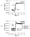
- a perspective view schematically showing a unit cell of GaN Perspective view showing basic vectors a 1 , a 2 , a 3 and c of wurtzite crystal structure (A) is a cross-sectional schematic diagram of the nitride-based semiconductor light emitting device 100 according to the embodiment of the present invention, (b) is a diagram showing an m-plane crystal structure, and (c) is a diagram showing a c-plane crystal structure. (A) to (c) are graphs showing the relationship between the work function (eV) of a metal in contact with GaN and the specific contact resistance ( ⁇ ⁇ cm 2 ).
- (A) is a graph showing the relationship between the Mg layer thickness (value after heat treatment) and the specific contact resistance in the Mg / Pt electrode
- (b) is a graph showing the specific contact resistance of the Pd / Pt electrode.
- (A) to (c) are photographs showing the surface state of the electrode after heat treatment when the Mg layer thickness is 2 nm, 15 nm, and 45 nm, respectively.
- (A) And (b) is the profile figure of the depth direction of Mg in the electrode structure (Mg / Pt) by SIMS analysis (A) And (b) is the profile figure of the depth direction of Ga in the electrode structure (Mg / Pt) by SIMS analysis (A) And (b) is the profile figure of the depth direction of N in the electrode structure (Mg / Pt) by SIMS analysis (A) And (b) is a drawing substitute photograph of a cross-sectional transmission electron microscope (TEM) of an electrode structure (Mg / Pt) in which an Mg layer is formed on an m-plane GaN layer.
- TEM cross-sectional transmission electron microscope
- (A) And (b) is the profile figure of the depth direction of Pt in the electrode structure (Mg / Pt) by SIMS analysis
- (A) is a figure which shows the cross section of the electrode structure (Mg / Pt) before heat processing which formed Mg layer on the m-plane GaN layer
- (b) is the cross section of the electrode structure (Mg / Pt) after heat processing.
- Illustration (A) is a graph showing current-voltage characteristics of a light emitting diode using an electrode made of an Mg / Pt layer
- (b) is a graph showing a contact resistance value of the light emitting diode.
- (A) is a graph showing contact resistance when an electrode made of an Au layer and an Mg / Au layer is used, and (b) and (c) show the surfaces of the electrodes of the Mg / Au layer and the Au layer, respectively.
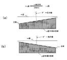
- Substitute photo of optical microscope (A) and (b) are graphs showing the hardness mapping of c-plane and m-plane GaN substrates, respectively.
- Sectional drawing which shows embodiment of a white light source
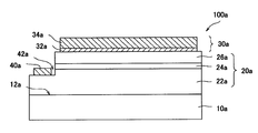
- Sectional drawing which shows the gallium nitride type compound semiconductor light-emitting device 100a which concerns on other embodiment of this invention.
- (A) is a figure which shows typically the crystal structure (wurtzite type crystal structure) of a GaN-type compound semiconductor
- (b) is the relationship between the normal of m surface, + c-axis direction, and a-axis direction
- a perspective view showing (A) And (b) is sectional drawing which shows the arrangement
- (A) And (b) is sectional drawing which shows typically the main surface and its vicinity area
- FIG. 3A schematically shows a cross-sectional configuration of the nitride-based semiconductor light-emitting device 100 according to the embodiment of the present invention.
- a nitride-based semiconductor light emitting device 100 shown in FIG. 3A is a semiconductor device made of a GaN-based semiconductor, and has a nitride-based semiconductor multilayer structure.
- the nitride-based semiconductor light-emitting device 100 of this embodiment is formed on a GaN-based substrate 10 having an m-plane as a surface 12, a semiconductor multilayer structure 20 formed on the GaN-based substrate 10, and the semiconductor multilayer structure 20.
- the electrode 30 is provided.
- the semiconductor multilayer structure 20 is an m-plane semiconductor multilayer structure formed by m-plane growth, and its surface is an m-plane. Since there are cases where a-plane GaN grows on an r-plane sapphire substrate, it is not always necessary that the surface of the GaN-based substrate 10 is an m-plane depending on the growth conditions.
- at least the surface of the p-type semiconductor region in contact with the electrode in the semiconductor multilayer structure 20 may be an m-plane.
- the nitride-based semiconductor light-emitting device 100 of the present embodiment includes the GaN substrate 10 that supports the semiconductor multilayer structure 20, but may include another substrate instead of the GaN substrate 10, or the substrate may be removed. It is also possible to use it in the state.
- FIG. 3B schematically shows a crystal structure in a cross section (cross section perpendicular to the substrate surface) of the nitride-based semiconductor whose surface is an m-plane. Since Ga atoms and nitrogen atoms exist on the same atomic plane parallel to the m-plane, no polarization occurs in the direction perpendicular to the m-plane. That is, the m-plane is a nonpolar plane, and no piezo electric field is generated in the active layer grown in the direction perpendicular to the m-plane.
- the added In and Al are located at the Ga site and replace Ga. Even if at least part of Ga is substituted with In or Al, no polarization occurs in the direction perpendicular to the m-plane.
- a GaN-based substrate having an m-plane on the surface is referred to as an “m-plane GaN-based substrate” in this specification.
- an m-plane GaN substrate is used and a semiconductor is grown on the m-plane of the substrate. This is because the surface orientation of the surface of the GaN-based substrate is reflected in the surface orientation of the semiconductor product structure.
- the surface of the substrate does not necessarily need to be an m-plane, and the substrate does not need to remain in the final device.
- FIG. 3C schematically shows a crystal structure in a nitride semiconductor cross section (cross section perpendicular to the substrate surface) having a c-plane surface.
- Ga atoms and nitrogen atoms do not exist on the same atomic plane parallel to the c-plane.
- polarization occurs in a direction perpendicular to the c-plane.
- a GaN-based substrate having a c-plane on the surface is referred to as a “c-plane GaN-based substrate” in this specification.
- the c-plane GaN-based substrate is a general substrate for growing GaN-based semiconductor crystals. Since the positions of the Ga atomic layer and the nitrogen atomic layer parallel to the c-plane are slightly shifted in the c-axis direction, polarization is formed along the c-axis direction.
- a semiconductor multilayer structure 20 is formed on the surface (m-plane) 12 of the m-plane GaN-based substrate 10.
- the Al d Ga e N layer 26 is located on the side opposite to the m-plane 12 side with respect to the active layer 24.
- the active layer 24 is an electron injection region in the nitride semiconductor light emitting device 100.
- the Al u Ga v In w N layer 22 of the present embodiment is a first conductivity type (n-type) Al u Ga v In w N layer 22.
- an undoped GaN layer may be provided between the active layer 24 and the Al d Ga e N layer 26.
- the Al composition ratio d need not be uniform in the thickness direction.
- the Al composition ratio d may change continuously or stepwise in the thickness direction. That is, the Al d Ga e N layer 26 may have a multilayer structure in which a plurality of layers having different Al composition ratios d are stacked, and the dopant concentration may also change in the thickness direction. .
- the uppermost part of the Al d Ga e N layer 26 (upper surface part of the semiconductor multilayer structure 20) is composed of a layer (GaN layer) in which the Al composition ratio d is zero. Is preferred.
- the Mg layer 32 described later is in contact with the GaN layer.
- the Al composition d may not be zero.
- Al 0.05 Ga 0.95 N having an Al composition d of about 0.05 can also be used.
- the Mg layer 32 described later is in contact with the Al 0.05 Ga 0.95 N layer.
- An electrode 30 is formed on the semiconductor multilayer structure 20.
- the electrode 30 of this embodiment is an electrode including an Mg layer 32 made of Mg, and a Pt layer made of Pt is formed on the Mg layer 32.
- the Mg layer 32 in the electrode 30 is in contact with the p-type semiconductor region of the semiconductor multilayer structure 20 and functions as a part of the p-type electrode (p-side electrode).
- the Mg layer 32 is in contact with the Al d Ga e N layer 26 doped with the second conductivity type (p-type) dopant.
- the Al d Ga e N layer 26 is doped with Mg as a dopant, for example.
- As a p-type dopant other than Mg for example, Zn or Be may be doped.
- the metal layer 34 in contact with the surface of the Mg layer 32 for example, a Pt layer or a metal layer that is difficult to form an alloy with Mg as compared with Au can be used.
- Au (gold) that easily forms an alloy with Mg is not preferable as the metal layer 34 that contacts the Mg layer 32.
- the Mg layer 32 is not alloyed with a metal such as Pt constituting the metal layer 34.
- not alloyed with a metal such as Pt includes a state in which a metal such as Pt is mixed in Mg at a concentration of less than% order (for example, 1%).
- “alloying with a metal such as Pt” means a state in which a metal such as Pt is mixed in Mg at a concentration of% order (for example, 1%) or more.
- the Mg layer 32 and the metal layer 34 may contain impurities and the like mixed in the manufacturing process of those layers.
- an alloy layer containing Mg may be formed between the Mg layer 32 and the metal layer 34.
- Pt, Mo, and Pd are metals that are less likely to be alloyed with Mg as compared with Au.
- an alloy layer can be formed by reacting with a part of the Mg layer 32 by heat treatment described later.
- all of the thin metal layer may be alloyed with a part of Mg in the Mg layer after the heat treatment. In this case, only the alloy layer exists on the Mg layer.
- an electrode layer or a wiring layer made of a metal or alloy other than these metals may be formed on each of the electrodes.
- the thickness of the electrode 30 of this embodiment is, for example, 10 to 200 nm.
- the thickness of the Mg layer 32 in the electrode 30 is, for example, 2 nm to 45 nm.
- the thickness of the Mg layer 32 is the thickness of the Mg layer after the heat treatment.
- the thickness of the metal layer 34 (a layer made of at least one metal selected from the group consisting of Pt, Mo, and Pd) located on the Mg layer 32 is, for example, 200 nm or less (or 10 nm to 200 nm). ).
- the Mg layer 32 is preferably thinner than the metal layer 34. This is to prevent peeling between the Mg layer 32 and the Al d Ga e N layer 26 due to the strain balance between the Mg layer 32 and the metal layer 34 being lost.
- the thickness of the GaN-based substrate 10 having the m-plane surface 12 is, for example, 100 to 400 ⁇ m. This is because there is no problem in handling the wafer if the substrate thickness is about 100 ⁇ m or more.
- the substrate 10 of the present embodiment may have a laminated structure as long as it has an m-plane surface 12 made of a GaN-based material. That is, the GaN-based substrate 10 of the present embodiment includes a substrate having an m-plane at least on the surface 12, and therefore, the entire substrate may be GaN-based or a combination with other materials. It doesn't matter.
- an electrode 40 (n-type electrode) is formed on a part of an n-type Al u Ga v In w N layer (for example, a thickness of 0.2 to 2 ⁇ m) 22 on the substrate 10.
- a recess 42 is formed in the region where the electrode 40 is formed in the semiconductor multilayer structure 20 so that a part of the n-type Al u Ga v In w N layer 22 is exposed.
- An electrode 40 is provided on the surface of the n-type Al u Ga v In w N layer 22 exposed at the recess 42.
- the electrode 40 is composed of, for example, a laminated structure of a Ti layer, an Al layer, and a Pt layer, and the thickness of the electrode 40 is, for example, 100 to 200 nm.
- the active layer 24 of the present embodiment includes a GaInN / GaN multiple quantum well (MQW) in which Ga 0.9 In 0.1 N well layers (eg, 9 nm thick) and GaN barrier layers (eg, 9 nm thick) are alternately stacked. It has a structure (for example, a thickness of 81 nm).
- MQW multiple quantum well
- a p-type Al d Ga e N layer 26 is provided on the active layer 24.
- the thickness of the p-type Al d Ga e N layer 26 is, for example, 0.2 to 2 ⁇ m.
- an undoped GaN layer may be provided between the active layer 24 and the Al d Ga e N layer 26.
- a second conductivity type (for example, p-type) GaN layer may be formed on the Al d Ga e N layer 26. Then, it is possible to form a contact layer made of p + -GaN on the GaN layer, and further form an Mg layer 32 on the contact layer made of p + -GaN.
- a contact layer made of GaN instead think of the Al d Ga e N layer 26 is another layer, it can be considered to be a part of the Al d Ga e N layer 26.
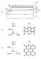
- FIGS. 4 (a) and 4 (b) are graphs showing the relationship between the work function (eV) of a metal in contact with m-plane GaN and the specific contact resistance ( ⁇ ⁇ cm 2 ). More specifically, FIGS. 4 (a) and 4 (b) show various metal layers (Mg layer thickness: 2 nm) on an Mg-doped p-type GaN layer (Mg concentration: about 1 ⁇ 10 19 cm ⁇ 3 ). The other metal layer thickness (200 nm) was formed, and the contact resistance was evaluated using a TLM (Transmission Line Method) method. “1.0E-01” shown on the vertical axis means “1.0 ⁇ 10 ⁇ 1 ”, and “1.0E-02” means “1.0 ⁇ 10 ⁇ 2 ”. , “1.0E + X” means “1.0 ⁇ 10 X ”.
- the contact resistance is generally inversely proportional to the contact area S (cm 2 ).
- R Rc
- the proportional constant Rc is referred to as a specific contact resistance and corresponds to the contact resistance R when the contact area S is 1 cm 2 . That is, the magnitude of the specific contact resistance does not depend on the contact area S and is an index for evaluating the contact characteristics.
- specific contact resistance may be abbreviated as “contact resistance”.
- FIG. 4A shows a case where heat treatment is not performed after metal formation (as-depo).
- FIG. 4B shows a case where Mg was heat-treated at 600 ° C. for 10 minutes in a nitrogen atmosphere, and Al, Au, Pd, Ni and Pt were heated at 500 ° C. for 10 minutes in a nitrogen atmosphere. The results when heat treatment is performed are shown. This difference in temperature is based on the fact that the contact resistance decreases most at 500 ° C. for metals other than Mg due to the difference in the optimum heat treatment temperature.
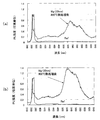
- FIG. 5A is a graph showing the relationship between the Mg layer thickness and the specific contact resistance in the Mg / Pt electrode (Pt is formed on Mg).
- the thickness of the Pt layer (before heat treatment) is fixed at 75 nm.
- FIG. 5B is a graph showing the specific contact resistance of a Pd / Pt electrode (Pd thickness 40 nm, Pt thickness: 35 nm) for comparison.
- the horizontal axis of the graph is the heat treatment temperature.
- the thickness of the metal layer other than the Mg layer is the thickness before the heat treatment.
- the data shown in FIG. 5 (a) is obtained from a sample in which an Mg layer is deposited using a pulse vapor deposition method.
- the pulse deposition method will be described later.
- the data shown in FIG. 5 (b) is obtained from a sample in which Pd and Pt layers are deposited using a normal electron beam evaporation method.
- the Mg layer is deposited by the pulse vapor deposition method.
- the Mg layer on the c-plane GaN layer is also deposited by pulse vapor deposition, but all metals other than Mg (Pd, Pt, Au) are deposited by ordinary electron beam vapor deposition. It is a thing.
- the Mg / Pt electrode and the Pd / Pt electrode are in contact with the m-plane GaN layer doped with Mg.
- Mg of 7 ⁇ 10 19 cm ⁇ 3 is doped in a region 20 nm deep from the surface (the outermost surface region having a thickness of 20 nm). Further, a region where the depth from the surface of the m-plane GaN layer exceeds 20 nm is doped with 1 ⁇ 10 19 cm ⁇ 3 of Mg.
- the concentration of the p-type impurity is locally increased in the outermost surface region of the GaN layer in contact with the p-type electrode, the contact resistance can be minimized.
- the horizontal axis in the graph of FIG. 5A indicates the thickness of the Mg layer after the heat treatment.
- the thickness of the Mg layer after the heat treatment is reduced as compared with that before the heat treatment.
- the thickness of the Mg layer before the heat treatment 600 ° C., 10 minutes
- the thickness of the Mg layer after the heat treatment was 2 nm.
- the thickness of the Mg layer before heat treatment 600 ° C., 10 minutes
- the thickness of the Mg layer after heat treatment was 45 nm and 15 nm, respectively.
- the graph of FIG. 5 (a) describes the experimental results showing the relationship between the measured value of contact resistance and the Mg thickness for a sample that has been heat-treated at 600 ° C. for 10 minutes. It was confirmed by experiment that the dependency of the contact resistance on the Mg layer thickness has the same tendency even under other heat treatment conditions.
- the contact resistance of the Mg / Pt electrode with respect to the m-plane GaN layer is the contact resistance of the Pd / Pt electrode with respect to the m-plane GaN layer (FIG. 5B ), which is almost the same size as that shown in FIG.
- FIG. 5A when the Mg layer thickness is 45 nm or less, the contact resistance is lower than that of the Pd / Pt electrode on the m-plane GaN, confirming the superiority of the present invention.
- the contact resistance decreased as the Mg layer thickness decreased.
- a sudden decrease in contact resistance was observed as the thickness of the Mg layer decreased from around 15 nm.
- the lowest contact resistance was obtained when the Mg layer thickness was around 2 nm.
- the thickness of the Mg layer 32 in the semiconductor element finally obtained through all the manufacturing steps including heat treatment is preferably 45 nm or less, and more preferably in the range of 2 nm to 15 nm. .
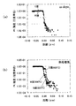
- 6 (a) to 6 (c) are photographs showing the surface state of the electrode after heat treatment when the Mg layer thickness is 2 nm, 15 nm, and 45 nm, respectively.
- the Mg layer thickness is a value after heat treatment at 600 ° C. for 10 minutes.
- electrode surface roughness (unevenness) was observed in the sample with the Mg layer thickness of 45 nm.
- the electrode surface roughness is considered to be a factor of increasing the contact resistance when the Mg layer thickness exceeds 45 nm.
- the Mg layer thickness exceeded 45 nm, a phenomenon that the Mg layer partially lifted was also observed. From observation with a transmission electron microscope, it was also confirmed that voids were generated at the interface between the Mg layer and the GaN layer. This is presumably because when the Mg layer thickness exceeds 45 nm, the strain of the Mg layer increases and the Mg layer peels off at the interface between Mg and GaN. From the above, it is preferable to set the thickness of the Mg layer to 45 nm or less.
- the Mg layer thickness is about 15 nm or less, the flatness of the electrode surface is extremely improved. For this reason, the Mg layer thickness is more preferably 15 nm or less.
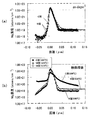
- FIG. 7 is a graph showing the contact resistance (measured value) when the contact surface is the m-plane and the c-plane for each contact resistance of the Mg / Pt electrode and the Pd / Pt electrode.
- the electrode is in contact with the p-type GaN layer.
- This p-type GaN layer is doped with Mg having the above-described concentration distribution.
- the heat treatment temperature and heat treatment time are as shown in Table 2 below.
- FIG. 8 shows a case where an Mg layer is formed on an m-plane (hereinafter referred to as “m-plane GaN”) of a p-type GaN layer, and a Pt layer is formed thereon (that is, m-plane GaN (Mg / Pt)). ) Result.
- the contact resistance of m-plane GaN is higher than that of c-plane GaN.
- an increase in contact resistance is observed at a heat treatment temperature exceeding 500 ° C.
- the m-plane GaN (Mg / Pt) electrode has a higher contact resistance than the Pd / Pt electrode when heat treatment is not performed. This is consistent with the common technical knowledge that a metal having a lower work function has a higher contact resistance.
- the heat treatment temperature is increased and the contact resistance is reduced.
- the contact resistance of m-plane GaN (Mg / Pt) is It becomes equal to or less than the contact resistance of m-plane GaN (Pd / Pt).
- the contact resistance of m-plane GaN (Mg / Pt) further decreases to be equivalent to the contact resistance of c-plane GaN (Mg / Pt), Even less.
- the contact resistance of m-plane GaN (Mg / Pt) becomes less than (or less than) the contact resistance of c-plane GaN (Mg / Pt).
- the contact resistance of m-plane GaN is lower than the contact resistance of both the m-plane and c-plane GaN (Mg / Pt) at a temperature of 600 ° C. Specifically, , About 1.0E-02 ⁇ cm ⁇ 2 or its periphery.
- the contact resistance of m-plane GaN (Mg / Pt) is higher than that at 600 ° C., but the m-plane and c-plane GaN (Mg / Pt) at 700 ° C. It becomes lower than any of the contact resistances.
- the heat treatment temperature of m-plane GaN is preferably, for example, 500 ° C. or higher.
- a predetermined temperature for example, 800 ° C.
- the vicinity of 600 ° C. is a more preferable heat treatment temperature.
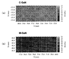
- FIG. 9 shows a photograph showing the surface state of the electrode after heat treatment at each temperature.
- FIG. 9 shows the results of As-depo (when no heat treatment is performed) and heat treatment temperatures of 500 ° C., 600 ° C., and 700 ° C.
- the Mg layer is formed on the p-type m-plane GaN layer and the Pt layer is formed thereon (in the case of M-GaN (Mg / Pt))
- slight unevenness is observed at a heat treatment temperature of 700 ° C.
- the surface Ra by AFM measurement was about 1.5 nm at 500 ° C., about 1.5 nm at 600 ° C., and about 4.5 nm at 700 ° C., and a good surface state was obtained.
- the Ra of the electrode surface is preferably about 4.5 nm or less, and more preferably about 1.5 nm or less.
- FIG. 10 shows the photoluminescence measurement results of the GaN layer when an Mg layer (30 nm) is formed on the GaN layer and heat-treated at 800 ° C. and 900 ° C. for 10 minutes.
- 10A shows the result of heat treatment at 800 ° C.
- FIG. 10B shows the result of heat treatment at 900 ° C.
- the PL intensity on the vertical axis in FIGS. 10A and 10B means the photoluminescence intensity.
- the PL intensity curve denoted as “Ref” obtained before the heat treatment is shown.
- the heat treatment temperature in the electrode using the Mg layer is desirably 700 ° C. or lower from the viewpoint of maintaining the quality of GaN.
- FIG. 11 shows the result of obtaining the profile of Mg atoms in the depth direction in the electrode structure (Mg / Pt) by using a secondary-ion-microprobe-mass-spectrometer (SIMS).
- FIG. 11 (a) shows the result when the heat treatment is not performed (as-depo) in the configuration in which the Mg layer is formed on the GaN layer (Mg / Pt electrode), while FIG. 11 (b) shows the heat treatment. Later results are shown.
- the temperature and time of the heat treatment are 10 minutes at 600 ° C. for c-plane GaN, 10 minutes at 600 ° C. and 10 minutes at 630 ° C. for m-plane GaN.
- the Mg layer thickness before the heat treatment is 7 nm, and the Pt layer thickness is 75 nm.
- the vertical axis represents the Mg concentration
- the horizontal axis represents the distance in the depth direction.
- the region where the numerical value on the horizontal axis is “ ⁇ ” is the electrode side, and the region “+” is the p-type GaN side.
- the origin (0 ⁇ m) on the horizontal axis is the peak position of Mg and substantially corresponds to the position of the interface between the p-type GaN layer and the Mg layer.
- ⁇ indicates data related to a sample having a heat treatment temperature of 600 ° C. formed on c-plane GaN. Further, “ ⁇ ” in the graph indicates data related to a sample formed on m-plane GaN with a heat treatment temperature of 600 ° C., and “ ⁇ ” indicates data related to a sample formed on m-plane GaN having a heat treatment temperature of 630 ° C. Is shown. The same applies to the graphs of FIGS. 12, 13, and 15 described later.
- the p-type GaN layer before the heat treatment is doped with 7 ⁇ 10 19 cm ⁇ 3 Mg in a region 20 nm deep from the surface of the p-type GaN layer in contact with the electrode.
- the deeper region is doped with 1 ⁇ 10 19 cm ⁇ 3 Mg.
- Mg on the c-plane GaN diffuses in the p-type GaN layer at a considerable concentration, as shown in FIG. It can also be seen that Mg is diffused in the Pt layer. On the other hand, it is confirmed that Mg on the m-plane GaN hardly diffuses in the p-type GaN layer and the Pt layer. More specifically, in the case of c-plane GaN, Mg diffuses deeply into the Pt layer after heat treatment, and also diffuses deeply into the GaN side. On the other hand, in the case of m-plane GaN, Mg slightly diffuses to the Pt layer side after heat treatment, but hardly diffuses to the GaN side.
- FIG. 12 shows the result of obtaining a profile in the depth direction of Ga atoms in the electrode structure (Mg / Pt) using SIMS.
- the Mg layer thickness before heat treatment is 7 nm
- the Pt layer thickness is 75 nm.
- the vertical axis of the graph shows the signal intensity of the SIMS detector, which is proportional to the atomic concentration.
- the distance 0 ⁇ m on the horizontal axis in FIG. 12 substantially corresponds to the position of the interface between the p-type GaN layer and the Mg layer.
- the origin (0 ⁇ m) on the horizontal axis was adjusted to the position of the Mg peak.
- the region where the numerical value on the horizontal axis is “ ⁇ ” is the electrode side, and the region “+” is the p-type GaN side.
- the vertical axis is normalized assuming that the Ga concentration in the as-depo GaN crystal is 1.
- the intensity of 1 ⁇ 10 ⁇ 3 on the vertical axis is approximately equivalent to 1 ⁇ 10 19 cm ⁇ 3 as the concentration.
- FIG. 12 (a) shows the result when heat treatment is not performed (as-depo) in the configuration in which the Mg layer is formed on the GaN layer (Mg / Pt electrode), while FIG. 12 (b) shows the heat treatment. Later results are shown.
- FIG. 12B two types of results with heat treatment temperatures of 600 ° C. and 630 ° C. are shown. The temperature and time of the heat treatment are 10 minutes at 600 ° C. for c-plane GaN, 10 minutes at 600 ° C. and 10 minutes at 630 ° C. for m-plane GaN.
- FIG. 12B it was confirmed that Ga was diffused in the Mg layer when heat treatment was performed.
- Ga diffusion is observed in the Mg layer, and the contact resistance is low.
- the contact resistance is low.
- Ga diffuses into the Mg layer and Pt layer, and Ga also moves into the electrode from the back in the GaN crystal.
- Ga is diffused significantly from the GaN layer into the electrode as a whole.
- m-plane GaN when the heat treatment temperature is 600 ° C., unlike c-plane GaN, Ga atoms seem to move only near the interface. It is presumed that atoms are less likely to move on the m-plane than on the c-plane.
- FIG. 13A is a graph showing a profile in the depth direction of nitrogen atoms in the Mg / Pt electrode before the heat treatment
- FIG. 13B is a profile in the depth direction of nitrogen atoms in the Mg / Pt electrode after the heat treatment. It is a graph which shows.
- the Mg layer thickness before heat treatment is 7 nm
- the Pt layer thickness is 75 nm.
- 13A and 13B the vertical axis represents the N intensity
- the horizontal axis represents the distance in the depth direction.
- N intensity of 1 ⁇ 10 -3 corresponds approximately to the N concentration of 1 ⁇ 10 19 cm -3.
- the region where the numerical value on the horizontal axis is “ ⁇ ” is the electrode side, and the region “+” is the p-type GaN side.
- the origin (0 ⁇ m) on the horizontal axis substantially corresponds to the position of the interface between the p-type GaN layer and the Mg layer.
- the electrode structure and p-type GaN doping conditions are the same as those in the sample described with reference to FIG.
- Ga vacancies have an acceptor property
- Ga vacancies increase near the interface between the electrode and p-type GaN
- holes easily pass through the Schottky barrier at this interface by tunneling.
- nitrogen atoms diffuse together with Ga atoms to the electrode side
- a nitrogen deficient state that is, nitrogen vacancies are also formed on the outermost surface of p-type GaN.
- Nitrogen vacancies have donor properties and cause charge compensation with Ga vacancies. For this reason, when not only Ga but nitrogen is diffused to the electrode side like c-plane GaN, the contact resistance is not particularly lowered.
- the relationship between the N (nitrogen) concentration and the Ga concentration in the Mg layer will be described in detail.
- the SIMS detected concentration of Ga in the Mg layer on the m-plane GaN layer was 4 ⁇ 1.0E-02.
- the detected intensity of SIMS is proportional to the atomic concentration. Therefore, when it is assumed that the Ga concentration of the base material of the GaN layer is about 1 ⁇ 10 22 cm ⁇ 3 , it is considered that Ga of about 4 ⁇ 10 19 cm ⁇ 3 exists in the Mg layer.
- the SIMS detection intensity was 3 ⁇ 1.0E-02. Based on the same assumption, it is considered that Ga of about 3 ⁇ 10 19 cm ⁇ 3 exists in the Mg layer on the m-plane GaN layer.
- the SIMS detection concentration of N (nitrogen) in the Mg layer on the m-plane GaN layer is the limit of detection sensitivity when heat treatment is performed at 600 ° C. and 630 ° C. 1 ⁇ 1.0E-03.
- N (nitrogen) contained in the Mg layer on the m-plane GaN layer is considered to be 1 ⁇ 10 18 cm ⁇ 3 or less.
- the Ga atom concentration in the Mg layer on the m-plane GaN layer is one digit (10 times) or more higher than the N atom concentration.
- Ga and N both have SIMS detection intensity of 1E-2 and both are present at about 1 ⁇ 10 19 cm ⁇ 3 . That is, the concentrations of Ga atoms and N atoms in the Mg layer on the c-plane GaN layer are approximately the same.
- FIG. 14 shows a cross-sectional transmission electron microscope (TEM) photograph of an electrode structure (Mg / Pt) in which an Mg layer is formed on an m-plane GaN layer.
- FIG. 14A shows the result when no heat treatment is performed (as-depo).
- FIG. 14B shows the result after heat treatment at 600 ° C. for 10 minutes.
- a 7 nm thick Mg layer was formed on the GaN crystal.
- the Pt layer eroded into the Mg layer after the heat treatment, and the thickness of the Mg layer became 2 nm.
- the Mg layer (the layer 32 in FIG. 3A) is thin (for example, 2 nm), but the Pt layer (the layer 34 in FIG. 3A).
- the presence of an Mg layer (layer 32 in FIG. 3A) made of Mg that was not alloyed or absorbed was confirmed.
- the existence of this thin Mg layer (32) is presumed to be one of the main factors that can reduce the contact resistance of m-plane GaN, which had a very large contact resistance in the prior art.
- FIG. 15 shows the result of obtaining a profile in the depth direction of Pt in the electrode structure (Mg / Pt) using SIMS.
- FIGS. 15A and 15B show the results when heat treatment is not performed (as-depo) and after the heat treatment, respectively, as in the above-described SIMS.
- the Mg layer thickness before heat treatment is 7 nm
- the Pt layer thickness is 75 nm.
- 15A and 15B the vertical axis represents the Pt intensity
- the horizontal axis represents the distance in the depth direction.
- Pt intensity of 1 ⁇ 10 -3 corresponds approximately to a Pt concentration of 1 ⁇ 10 19 cm -3.
- the region where the numerical value on the horizontal axis is “ ⁇ ” is the electrode side, and the region “+” is the p-type GaN side.
- the origin (0 ⁇ m) on the horizontal axis substantially corresponds to the position of the interface between the p-type GaN layer and the Mg layer.
- the electrode structure and p-type GaN doping conditions are the same as those in the sample described with reference to FIG.
- FIG. 16A is a schematic diagram showing the Mg / Pt electrode structure before the heat treatment.
- FIG. 16B is a schematic diagram showing the Mg / Pt electrode structure before the heat treatment. All drawings were prepared based on the cross-sectional TEM.
- the thickness of the deposited Mg layer exceeds 5 nm, the thickness of the Mg layer is reduced by the heat treatment at 600 ° C. for 10 minutes, but the Mg layer exists as a substantially continuous film even after the heat treatment.
- the thickness at the time of deposition of the Mg layer is about 2 nm, after heat treatment at 600 ° C. for 10 minutes, as shown in FIG. It was confirmed that the islands may exist.
- the thickness of the Mg layer immediately after deposition is about 2 nm, the morphology of the finally obtained Mg layer may be varied depending on the conditions of the heat treatment to be performed.
- the “Mg layer” in this specification includes a collection of a large number of island-like (island-like) Mg existing on the surface of the p-type semiconductor region. Further, the “Mg layer” may be composed of a film having a plurality of openings (for example, a porous film). Thus, if Mg that is not eroded by Pt is in contact with the surface (m-plane) of the p-type semiconductor region, a contact resistance reduction effect can be sufficiently obtained.
- contact resistance reduction effect substantially the same result (contact resistance reduction effect) can be obtained when a Mo layer or a Pd layer is deposited on the Mg layer instead of the Pt layer.
- the important point from the viewpoint of obtaining the contact resistance reduction effect is that the Mg layer and the GaN-based semiconductor are in contact with each other, and the metal on the Mg layer is formed from a material that is difficult to form an alloy with Mg as compared with Au. There is to be.
- an m-plane GaN substrate 10 and an Al u Ga v In w N layer (u + v + w 1, u ⁇ 0, v ⁇ 0, w ⁇ 0) 22.
- the m-plane GaN substrate 10 is an n-type GaN substrate (for example, a thickness of 100 ⁇ m)
- the Al u Ga v In w N layer 22 is an n-type GaN layer (for example, a thickness of 2 ⁇ m).
- An active layer 24 is formed on the Al u Ga v In w N layer 22.
- the semiconductor multilayer structure 20 including at least the active layer 24 is formed on the m-plane GaN substrate 10.
- the active layer 24 is composed of, for example, an InGaN well layer and a GaN barrier layer having an In composition ratio of about 25%, the well layer thickness is 9 nm, the barrier layer thickness is 9 nm, and the well layer period is three periods. .
- the Al d Ga e N layer 26 of this embodiment is doped with Mg as a p-type dopant.
- Mg is doped to the Al d Ga e N layer 26 by, for example, about 10 18 cm ⁇ 3 .
- an undoped GaN layer (not shown) is formed between the active layer 24 and the Al d Ga e N layer 26.
- a second conductivity type (for example, p-type) GaN layer (not shown) is formed on the Al d Ga e N layer 26.
- an Mg layer 32 is formed on the contact layer made of p + -GaN, and a Pt layer 34 is formed thereon.
- the laminated structure of the Mg layer 32 and the Pt layer 34 becomes an electrode (p-type electrode) 30.
- the semiconductor multilayer structure 20, Al u Ga v In w recess (recess) 42 for exposing the surface of the N layer 22 is formed, it is located on the bottom surface of the recess 42 Al u Ga v In w N layer 22
- An electrode (n-type electrode) 40 is formed on the substrate.
- the size of the recess 42 is, for example, a width (or diameter) of 20 ⁇ m and a depth of 1 ⁇ m.
- the electrode 40 is, for example, an electrode having a laminated structure of a Ti layer, an Al layer, and a Pt layer (for example, the thickness is 5 nm, 100 nm, and 10 nm, respectively).
- the operating voltage (Vop) can be reduced by about 1.5 V compared to the case of a conventional m-plane LED using a Pd / Pt electrode, and as a result. It was found that power consumption can be reduced.
- an m-plane substrate 10 is prepared.
- a GaN substrate is used as the substrate 10.
- the GaN substrate of the present embodiment is obtained by using an HVPE (Hydride Vapor Phase Epitaxial) method.
- a thick film GaN on the order of several mm is grown on a c-plane sapphire substrate.
- an m-plane GaN substrate is obtained by cutting the thick film GaN in the direction perpendicular to the c-plane and the m-plane.
- the production method of the GaN substrate is not limited to the above, and a method of producing an ingot of bulk GaN using a liquid phase growth method such as a sodium flux method or a melt growth method such as an ammonothermal method, and cutting it in the m plane But it ’s okay.
- a gallium oxide, a SiC substrate, a Si substrate, a sapphire substrate, or the like can be used in addition to a GaN substrate.
- the plane orientation of the SiC or sapphire substrate is preferably the m-plane.
- the growth surface may not necessarily be the m-plane depending on the growth conditions. It is sufficient that at least the surface of the semiconductor multilayer structure 20 is m-plane.
- crystal layers are sequentially formed on the substrate 10 by MOCVD (Metal Organic Organic Chemical Vapor Deposition) method.
- an Al u Ga v In w N layer 22 is formed on the m-plane GaN substrate 10.
- Al u Ga v In w N layer 22 for example, AlGaN having a thickness of 3 ⁇ m is formed.
- a GaN layer is formed by supplying TMG (Ga (CH 3 ) 3 ), TMA (Al (CH 3 ) 3 ), and NH 3 on the m-plane GaN substrate 10 at 1100 ° C. accumulate.
- the active layer 24 is formed on the Al u Ga v In w N layer 22.
- the active layer 24 has a GaInN / GaN multiple quantum well (MQW) structure with a thickness of 81 nm in which a Ga 0.9 In 0.1 N well layer with a thickness of 9 nm and a GaN barrier layer with a thickness of 9 nm are alternately stacked.
- MQW multiple quantum well
- the growth temperature is preferably lowered to 800 ° C. in order to incorporate In.
- an Al d Ga e N layer 26 is formed on the undoped GaN layer.
- the Al d Ga e N layer 26 for example, by supplying TMG, NH 3 , TMA, TMI and Cp 2 Mg (cyclopentadienyl magnesium) as a p-type impurity, p-Al 0.14 Ga 0.86 having a thickness of 70 nm is provided. N is formed.
- Cp 2 Mg is supplied as a p-type impurity.
- the p-GaN contact layer, the Al d Ga e N layer 26, the undoped GaN layer, and a part of the active layer 24 are removed to form a recess 42, and Al x Ga y InzN
- the n-type electrode formation region of the layer 22 is exposed.
- a Ti / Pt layer is formed as the n-type electrode 40 on the n-type electrode formation region located at the bottom of the recess 42.
- an Mg layer 32 is formed on the p-GaN contact layer, and a Pt layer 34 is further formed on the Mg layer 32. Thereby, the p-type electrode 40 is formed.
- a technique pulse deposition method
- Mg metal in a crucible held in a vacuum is irradiated with an electron beam in a pulse manner to evaporate the source metal in a pulse manner.
- the source metal molecules or atoms adhere to the p-GaN contact layer, and the Mg layer 32 is formed.
- the pulse has a pulse width of 0.5 seconds and a repetition of 1 Hz.
- the pulse width is preferably 0.005 seconds to 5 seconds, and the pulse frequency is preferably 0.1 Hz to 100 Hz.
- the Mg layer 32 a dense and good quality film was formed as the Mg layer 32.
- the reason why the Mg layer becomes dense is thought to be that the kinetic energy of Mg atoms or Mg atom clusters that collide with the p-GaN contact layer is increased by performing pulse deposition. That is, due to the electron beam irradiation, a part of the raw material Mg instantaneously becomes Mg atoms having high energy and is vaporized or evaporated. Then, Mg atoms reach the p-GaN contact layer.
- Mg atoms that have reached the p-GaN contact layer undergo migration and form a dense and homogeneous Mg thin film at the atomic level.
- An Mg thin film of about 1 to 20 atomic layers is formed by one pulse of electron beam. By repeatedly irradiating the pulsed electron beam, the Mg thin film is laminated on the p-GaN contact layer, and the Mg layer 32 having a desired thickness is formed.
- the electron beam preferably has a high peak intensity so that the kinetic energy necessary for the migration of Mg atoms after migration can be supplied to the Mg atoms.
- the driving power of the electron gun it is preferable to determine the driving power of the electron gun so that the Mg thin film is formed with a thickness of 20 atomic layers (approximately 5 nm) or less per one pulse of the electron beam. If the Mg thin film formed per one pulse of the electron beam is thicker than the 20 atomic layer, it becomes difficult to obtain a dense and homogeneous Mg thin film. A more preferred deposition rate is 5 atomic layers or less per pulse of the electron beam. This is because when there are too many Mg atoms, the Mg atoms collide during the migration, thereby losing the kinetic energy of the Mg atoms.
- Mg is an element that is easily oxidized by contact with water or air.
- the Mg thin film formed on a support substrate by a normal vapor deposition method When placed in the atmosphere, it is rapidly oxidized. As a result, the Mg thin film gradually loses metallic luster and eventually becomes tattered and peels off from the support.
- the Mg layer 32 formed by the forming method (pulse vapor deposition) of the present embodiment is dense and homogeneous at the atomic level, and has a structure in which the atomic arrangement is very well arranged as epitaxially grown. . And there are few pinholes that are considered to be the cause of oxidation, and it is difficult to be oxidized. A beautiful mirror surface can be maintained even after being left in the atmosphere for several months.
- Mg has the property of being vaporized at once when its melting point is exceeded. For this reason, it is very difficult to accurately control the thickness of the Mg thin film to be formed on the nanometer order by adjusting the deposition rate of the Mg thin film.
- the thickness of the Mg layer 32 created by the forming method of the present embodiment can be accurately controlled on the nanometer order by appropriately setting the irradiation time of the pulsed electron beam.
- the forming method of the present embodiment is also effective when an Mg thin film is formed on a Si substrate or a glass substrate. Therefore, the formation method of this embodiment is not limited to GaN, and an Mg thin film can be formed on various types of materials. And the formation method of this embodiment can be used suitably especially for formation of the electrode in the semiconductor field
- the Mg layer 32 created by the forming method of the present embodiment is stable even when heat treatment is performed at a temperature of 600 ° C. or higher.
- a technique of performing vapor deposition while vaporizing the source metal (Mg metal) in a pulsed manner is adopted, but other techniques can be adopted as long as the Mg layer 32 can be formed. It is.
- a thermal CVD method or molecular beam epitaxy (MBE) can be employed as another method for forming a dense and high-quality Mg layer.
- the substrate 10 and part of the Al u Ga v In w N layer 22 may be removed by using a method such as laser lift-off, etching, and polishing. In this case, only the substrate 10 may be removed, or only a part of the substrate 10 and the Al u Ga v In w N layer 22 may be selectively removed. Of course x, substrate 10, Al u Ga v may be left without removing an In w N layer 22.
- the nitride-based semiconductor light-emitting device 100 of this embodiment is formed.
- nitride-based semiconductor light emitting device 100 of the present embodiment when a voltage is applied between the n-type electrode 40 and the p-type electrode 30, holes are transferred from the p-type electrode 30 toward the active layer 24. Electrons are injected from the active layer 24 toward the active layer 24 to emit light having a wavelength of 450 nm, for example.
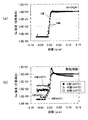
- FIG. 17A shows current-voltage characteristics of a light emitting diode using an electrode made of an Mg / Pt layer on m-plane GaN.
- the nitride semiconductor structure of the light emitting diode is the same, the characteristics of the light emitting diode using the electrode made of the Pd / Pt layer, and the light emitting diode using the electrode made of the Mg / Pt layer on the c-plane GaN
- the characteristics of The electrode configuration and heat treatment conditions in these three types of light emitting diodes are as shown in Table 4 below.
- This light-emitting diode has a configuration in which an n-type GaN layer, an InGaN well layer (three layers) and a GaN barrier layer (two layers) are alternately stacked on an m-plane or c-plane GaN substrate, p-type GaN Layers are stacked. Further, an Mg / Pt electrode or a Pd / Pt electrode is provided as a p-type electrode on the p-type GaN layer. The n-type electrode is formed on the n-type GaN layer by etching the p-type GaN layer and the active layer to expose the n-type GaN layer.
- the current value becomes the voltage value. It increases with the increase.
- the rising voltage is about 3.1 V in the case of an electrode (on m-plane GaN) made of a Pd / Pt layer.
- the rising voltage in the case of the electrode (on the m-plane GaN) made of the Mg / Pt layer is about 2.5 V, and a reduction is observed. It is confirmed that the operating voltage at which the current value on the vertical axis is 20 mA is reduced by 1.5 V or more in the electrode made of the Mg / Pt layer compared to the electrode made of the Pd / Pt layer.
- a light-emitting diode (m-plane light-emitting diode) using an electrode made of an Mg / Pt layer on m-plane GaN and a light-emitting diode (c-plane light-emitting diode) using an electrode made of an Mg / Pt layer on c-plane GaN
- the rising voltage is lower than that of the c-plane light emitting diode, and the effect of reducing the contact resistance is confirmed.
- a current value of 20 mA is obtained at a driving voltage of 3.2 V.
- the c-surface light emitting diode has a current value of 4.8 mA at the same driving voltage. Since the light output of the light emitting diode depends on the current value, it can be seen that the m-plane light emitting diode can obtain a light output nearly four times that of the c surface light emitting diode at the driving voltage of 3.2 V.
- a light-emitting diode is a diode having a pn junction therein, and a curve indicating current-voltage characteristics of a pn junction diode is generally approximated by the following equation.
- I I 0 exp (V / n ⁇ KT)
- I is a current value flowing through a pn junction diode
- I 0 is a current constant
- V is an applied voltage
- K is a Boltzmann constant
- T is a temperature
- the value of the contact resistance of this light emitting diode was 3.8 ⁇ 10 ⁇ 4 ⁇ cm 2 for the electrode made of the Mg / Pt layer.
- Such a contact resistance value of 10 minus 4 is the first example in p-type m-plane GaN, and this is a surprising result. It has been found that this can reduce power consumption. In addition, it has been found that m-plane GaN devices can provide extremely great technical significance. In the case of an electrode composed of a Pd / Pt layer, the value was about 1 ⁇ 10 ⁇ 2 ⁇ cm 2 .
- FIG. 18A shows the result of forming an Au layer or Mg / Au layer electrode on an m-plane GaN layer and measuring its specific contact resistance ( ⁇ ⁇ cm 2 ).
- the specific contact resistance is a value of the specific contact resistance after the electrode is formed and heat treatment is performed.
- the characteristic of the specific contact resistance is worse when the Mg / Au layer electrode is used than when the Au layer electrode is used.
- This point is significantly different from the result of the characteristic improvement in the configuration of the electrode (for example, Mg / Pt layer) of the present embodiment.
- Mg is an element that is easily oxidized by contact with water or air
- the structure used as a laminate of Mg layers (Mg / Au layer) instead of a single electrode of Mg layer is Can be one of the candidates for consideration.
- the contact resistance of the Mg / Au layer is increased as compared with the Au layer, so that the contact characteristics are poor.
- the excellent contact resistance characteristics of the configuration of the present embodiment is that the results of the case where the Au layer is stacked on the Mg layer are bad for those skilled in the art. It seems to have had an unpredictable effect.
- FIG. 18B is a drawing-substituting photograph showing the surface of the Mg / Au layer electrode after the heat treatment
- FIG. 18C is a drawing-substituting photograph showing the surface of the Au layer electrode after the heat treatment. It is a photograph. When both were compared, it was found that the film quality of the Mg / Au layer electrode was worse.
- FIG. 19 shows hardness mapping (5 mN, 1 ⁇ m conical) using a Conical chip.
- FIG. 19A shows the result of the c-plane GaN substrate (C-GaN)
- FIG. 19B shows the result of the m-plane GaN substrate (M-GaN).
- Patent Documents 3 and 4 have no description that the crystal plane of the gallium nitride-based semiconductor layer is the m-plane, and therefore, the disclosure of these documents discloses an electrode on the c-plane gallium nitride-based semiconductor layer. It is related to the technology that formed.
- Patent Document 3 relates to a structure in which an Au layer is laminated on an Mg layer, and even if an electrode having the laminated structure is formed on the m-plane, the effect of the electrode of this embodiment can be obtained. Not.
- Patent Document 4 refers to a metal layer made of Ni, Cr, and Mg, but the disclosed examples are only those having an electrode structure with a Ni layer as a lower layer.
- Patent Documents 3 and 4 both relate to an electrode structure formed on a c-plane gallium nitride semiconductor layer, and neither a problem nor a solution regarding contact resistance to an m-plane gallium nitride semiconductor layer is taught.
- the light emitting device may be used as a light source as it is.
- the light-emitting element according to the present invention can be suitably used as a light source (for example, a white light source) having an extended wavelength band when combined with a resin or the like including a fluorescent material for wavelength conversion.
- FIG. 20 is a schematic diagram showing an example of such a white light source.
- the light source of FIG. 20 includes a light emitting element 100 having the configuration shown in FIG. 3A and a phosphor that converts the wavelength of light emitted from the light emitting element 100 into a longer wavelength (for example, YAG: Yttrium Aluminum Garnet). And a resin layer 200 in which is dispersed.
- the light emitting element 100 is mounted on a support member 220 having a wiring pattern formed on the surface, and a reflection member 240 is disposed on the support member 220 so as to surround the light emitting element 100.
- the resin layer 200 is formed so as to cover the light emitting element 100.
- the p-type semiconductor region in contact with the Mg layer 32 is made of GaN or AlGaN
- a layer containing In, for example, InGaN may be used.
- “In 0.2 Ga 0.8 N” with an In composition of 0.2, for example, can be used for the contact layer in contact with the electrode 30.
- the effect of reducing the contact resistance can naturally be obtained in light emitting elements (semiconductor lasers) other than LEDs and devices other than light emitting elements (for example, transistors and light receiving elements).
- the actual surface (main surface) of the m-plane semiconductor layer does not need to be a plane that is completely parallel to the m-plane, and is inclined at a slight angle (greater than 0 ° and less than ⁇ 1 °) from the m-plane. May be. It is difficult to form a substrate or a semiconductor layer having a surface that is completely parallel to the m-plane from the viewpoint of manufacturing technology. For this reason, when an m-plane substrate or an m-plane semiconductor layer is formed by the current manufacturing technology, the actual surface is inclined from the ideal m-plane. Since the inclination angle and orientation vary depending on the manufacturing process, it is difficult to accurately control the inclination angle and inclination orientation of the surface.
- the surface (main surface) of the substrate or semiconductor is intentionally inclined at an angle of 1 ° or more from the m-plane.
- the gallium nitride-based compound semiconductor light-emitting element in the embodiment described below includes a p-type semiconductor region having a main surface that is inclined at an angle of 1 ° or more from the m-plane.
- FIG. 21 is a cross-sectional view showing the gallium nitride compound semiconductor light emitting device 100a of this embodiment.
- the gallium nitride-based compound semiconductor light emitting device 100a In order to form a p-type semiconductor region whose main surface is a surface inclined at an angle of 1 ° or more from the m-plane, the gallium nitride-based compound semiconductor light emitting device 100a according to this embodiment has an angle of 1 ° or more from the m-plane.
- a GaN substrate 10a whose main surface is an inclined surface is used.
- a substrate whose main surface is inclined at an angle of 1 ° or more from the m-plane is generally referred to as an “off substrate”.
- the off-substrate can be manufactured by slicing the substrate from the single crystal ingot and polishing the surface of the substrate so that the main surface is intentionally inclined in a specific direction from the m-plane.
- a semiconductor multilayer structure 20a is formed on the GaN substrate 10a.
- the semiconductor layers 22a, 24a, and 26a shown in FIG. 21 are inclined at an angle of 1 ° or more from the m-plane. This is because when various semiconductor layers are stacked on the inclined main surface of the substrate, the surfaces (main surfaces) of these semiconductor layers are also inclined from the m-plane.
- a sapphire substrate or SiC substrate having a surface inclined in a specific direction from the m-plane may be used.
- FIG. 22 (a) is a diagram schematically showing a crystal structure (wurtzite crystal structure) of a GaN-based compound semiconductor, and shows a structure obtained by rotating the crystal structure of FIG. 2 by 90 °.
- the + c plane is a (0001) plane in which Ga atoms appear on the surface, and is referred to as a “Ga plane”.
- the ⁇ c plane is a (000-1) plane in which N (nitrogen) atoms appear on the surface, and is referred to as an “N plane”.
- the + c plane and the ⁇ c plane are parallel to each other, and both are perpendicular to the m plane. Since the c-plane has polarity, the c-plane can be divided into a + c-plane and a ⁇ c-plane in this way, but there is no significance in distinguishing the non-polar a-plane into the + a-plane and the ⁇ a-plane. .
- the + c-axis direction shown in FIG. 22A is a direction extending perpendicularly from the ⁇ c plane to the + c plane.
- the a-axis direction corresponds to the unit vector a 2 in FIG. 2 and faces the [-12-10] direction parallel to the m-plane.
- FIG. 22B is a perspective view showing the correlation between the normal of the m-plane, the + c-axis direction, and the a-axis direction.
- the normal of the m-plane is parallel to the [10-10] direction and is perpendicular to both the + c-axis direction and the a-axis direction, as shown in FIG.
- the fact that the main surface of the GaN-based compound semiconductor layer is inclined at an angle of 1 ° or more from the m-plane means that the normal line of the main surface of the semiconductor layer is inclined at an angle of 1 ° or more from the normal line of the m-plane. means.
- FIGS. 23A and 23B are cross-sectional views showing the relationship between the main surface and the m-plane of the GaN-based compound semiconductor layer, respectively.
- This figure is a cross-sectional view perpendicular to both the m-plane and the c-plane.
- FIG. 23 shows an arrow indicating the + c-axis direction.
- the m-plane is parallel to the + c-axis direction. Accordingly, the normal vector of the m-plane is perpendicular to the + c axis direction.
- the normal vector of the main surface in the GaN-based compound semiconductor layer is inclined in the c-axis direction from the normal vector of the m-plane. More specifically, in the example of FIG. 23 (a), the normal vector of the principal surface is inclined toward the + c plane, whereas in the example of FIG. 23 (b), the normal vector of the principal surface is ⁇ Inclined to the c-plane side.
- the inclination angle (inclination angle ⁇ ) of the normal vector of the principal surface with respect to the normal vector of the m plane in the former case is a positive value, and the inclination angle ⁇ in the latter case is a negative value. I will decide. In either case, it can be said that “the main surface is inclined in the c-axis direction”.
- FIGS. 24A and 24B are cross-sectional views corresponding to FIGS. 23A and 23B, respectively, and show the vicinity of the main surface in the p-type semiconductor region inclined in the c-axis direction from the m-plane. Show.
- each step has a height equivalent to a monoatomic layer (2.7 mm) and is arranged in parallel at substantially equal intervals (30 mm or more).
- a main surface inclined from the m-plane as a whole is formed, but it is considered that a large number of m-plane regions are exposed microscopically.
- FIG. 25 is a cross-sectional TEM photograph of the p-type semiconductor region tilted by 1 ° from the m-plane in the ⁇ c-axis direction.
- the m-plane is clearly exposed on the surface of the p-type semiconductor region, and it is confirmed that the inclination is formed by atomic steps.
- the surface of the GaN-based compound semiconductor layer whose main surface is inclined from the m-plane has such a structure because the m-plane is originally very stable as a crystal plane.
- a similar phenomenon is considered to occur even if the inclination direction of the normal vector of the main surface is oriented to a plane orientation other than the + c plane and the ⁇ c plane.
- Even if the normal vector of the main surface is inclined in the a-axis direction, for example, the same can be considered if the inclination angle is in the range of 1 ° to 5 °.
- the contact resistance does not depend on the inclination angle.
- an Mg / Pt layer electrode is formed on a p-type semiconductor region inclined by 0 °, 2 °, or 5 ° in the ⁇ c axis direction from the m-plane, and the contact resistance ( ⁇ ⁇ cm 2 ) is shown.
- the vertical axis of the graph is the specific contact resistance
- the horizontal axis is the inclination angle (angle formed by the normal of the m-plane and the normal of the surface in the p-type semiconductor region) ⁇ .
- the specific contact resistance is a value of the specific contact resistance after the electrode is formed and heat treatment is performed. As can be seen from the results in FIG. 26, when the inclination angle ⁇ is 5 ° or less, the contact resistance has a substantially constant value.
- the absolute value of the inclination angle ⁇ is limited to 5 ° or less.
- the actual inclination angle ⁇ may be shifted from 5 ° by about ⁇ 1 ° due to manufacturing variations. It is difficult to completely eliminate such manufacturing variations, and such a small angular deviation does not hinder the effects of the present invention.
- the semiconductor light emitting device in this embodiment it can be suitably used as a light source (for example, a white light source) having an extended wavelength band in combination with a resin including a fluorescent material.
- the contact resistance can be reduced in a GaN-based semiconductor element crystal-grown on an m-plane substrate or a GaN-based semiconductor multilayer structure having an m-plane as a surface. Therefore, GaN-based semiconductor elements grown on crystals on m-plane substrates (or GaN-based semiconductor multilayer structures with m-plane surfaces), which have been difficult to actively use due to poor contact resistance characteristics, have been heretofore used.
Landscapes
- Engineering & Computer Science (AREA)
- Manufacturing & Machinery (AREA)
- Computer Hardware Design (AREA)
- Microelectronics & Electronic Packaging (AREA)
- Power Engineering (AREA)
- Led Devices (AREA)
- Electrodes Of Semiconductors (AREA)
- Semiconductor Lasers (AREA)
Priority Applications (5)
| Application Number | Priority Date | Filing Date | Title |
|---|---|---|---|
| KR1020127006658A KR101171722B1 (ko) | 2009-12-25 | 2010-12-21 | 질화물계 반도체 소자 및 그의 제조방법 |
| EP10838943.8A EP2479807B1 (en) | 2009-12-25 | 2010-12-21 | Nitride semiconductor light emitting diode |
| CN2010800410415A CN102511085A (zh) | 2009-12-25 | 2010-12-21 | 氮化物系半导体元件及其制造方法 |
| JP2011520266A JP4843122B2 (ja) | 2009-12-25 | 2010-12-21 | 窒化物系半導体素子およびその製造方法 |
| US13/447,368 US8748899B2 (en) | 2009-12-25 | 2012-04-16 | Nitride-based semiconductor device and method for fabricating the same |
Applications Claiming Priority (2)
| Application Number | Priority Date | Filing Date | Title |
|---|---|---|---|
| JP2009-294617 | 2009-12-25 | ||
| JP2009294617 | 2009-12-25 |
Related Child Applications (1)
| Application Number | Title | Priority Date | Filing Date |
|---|---|---|---|
| US13/447,368 Continuation US8748899B2 (en) | 2009-12-25 | 2012-04-16 | Nitride-based semiconductor device and method for fabricating the same |
Publications (1)
| Publication Number | Publication Date |
|---|---|
| WO2011077704A1 true WO2011077704A1 (ja) | 2011-06-30 |
Family
ID=44195258
Family Applications (1)
| Application Number | Title | Priority Date | Filing Date |
|---|---|---|---|
| PCT/JP2010/007400 WO2011077704A1 (ja) | 2009-12-25 | 2010-12-21 | 窒化物系半導体素子およびその製造方法 |
Country Status (6)
| Country | Link |
|---|---|
| US (1) | US8748899B2 (zh) |
| EP (1) | EP2479807B1 (zh) |
| JP (1) | JP4843122B2 (zh) |
| KR (1) | KR101171722B1 (zh) |
| CN (1) | CN102511085A (zh) |
| WO (1) | WO2011077704A1 (zh) |
Families Citing this family (1)
| Publication number | Priority date | Publication date | Assignee | Title |
|---|---|---|---|---|
| JP7244745B2 (ja) * | 2019-02-15 | 2023-03-23 | 日亜化学工業株式会社 | 発光装置、及び、光学装置 |
Citations (10)
| Publication number | Priority date | Publication date | Assignee | Title |
|---|---|---|---|---|
| JPH0711430A (ja) * | 1993-06-29 | 1995-01-13 | Mitsubishi Electric Corp | 電子ビーム蒸着装置と電子ビームを用いた溶接装置及び自由電子レーザ装置 |
| JPH0864871A (ja) | 1994-08-22 | 1996-03-08 | Nichia Chem Ind Ltd | 窒化ガリウム系化合物半導体素子 |
| JPH1140846A (ja) | 1997-07-15 | 1999-02-12 | Nec Corp | 窒化ガリウム系半導体のp型電極およびその形成方法 |
| JPH11274554A (ja) * | 1998-03-26 | 1999-10-08 | Toshiba Corp | III−V族化合物半導体発光素子のp側電極及びIII−V族化合物半導体発光素子 |
| JP2001160656A (ja) * | 1999-12-01 | 2001-06-12 | Sharp Corp | 窒化物系化合物半導体装置 |
| JP2001308462A (ja) | 2000-04-21 | 2001-11-02 | Matsushita Electric Ind Co Ltd | 窒化物半導体素子の製造方法 |
| JP2003332697A (ja) | 2002-05-09 | 2003-11-21 | Sony Corp | 窒化物半導体素子及びその製造方法 |
| JP2008153285A (ja) * | 2006-12-14 | 2008-07-03 | Rohm Co Ltd | 窒化物半導体装置および窒化物半導体製造方法 |
| WO2010103804A1 (ja) * | 2009-03-11 | 2010-09-16 | パナソニック株式会社 | 窒化物系半導体素子およびその製造方法 |
| WO2010116703A1 (ja) * | 2009-04-06 | 2010-10-14 | パナソニック株式会社 | 窒化物系半導体素子およびその製造方法 |
Family Cites Families (43)
| Publication number | Priority date | Publication date | Assignee | Title |
|---|---|---|---|---|
| JPH0711429A (ja) | 1993-06-23 | 1995-01-13 | Toshiba Corp | 金属蒸気発生方法および装置 |
| US5708301A (en) | 1994-02-28 | 1998-01-13 | Sumitomo Chemical Company, Limited | Electrode material and electrode for III-V group compound semiconductor |
| US6072197A (en) | 1996-02-23 | 2000-06-06 | Fujitsu Limited | Semiconductor light emitting device with an active layer made of semiconductor having uniaxial anisotropy |
| JP3735960B2 (ja) * | 1996-09-06 | 2006-01-18 | 松下電器産業株式会社 | 半導体発光素子 |
| JPH10341039A (ja) | 1997-04-10 | 1998-12-22 | Toshiba Corp | 半導体発光素子およびその製造方法 |
| JP4013288B2 (ja) | 1997-06-25 | 2007-11-28 | 住友化学株式会社 | 3−5族化合物半導体用電極の製造方法と3−5族化合物半導体素子 |
| JPH11233890A (ja) | 1998-02-12 | 1999-08-27 | Matsushita Electric Ind Co Ltd | 窒化ガリウム系化合物半導体素子 |
| JP4183299B2 (ja) * | 1998-03-25 | 2008-11-19 | 株式会社東芝 | 窒化ガリウム系化合物半導体発光素子 |
| JP2000049114A (ja) * | 1998-07-30 | 2000-02-18 | Sony Corp | 電極およびその形成方法ならびに半導体装置およびその製造方法 |
| JP3525061B2 (ja) * | 1998-09-25 | 2004-05-10 | 株式会社東芝 | 半導体発光素子の製造方法 |
| JP2000174333A (ja) * | 1998-12-02 | 2000-06-23 | Toshiba Corp | 窒化ガリウム系化合物半導体発光素子及び製造方法 |
| JP4627850B2 (ja) | 1999-09-09 | 2011-02-09 | シャープ株式会社 | Iii族窒化物半導体の電極形成方法 |
| JP3929008B2 (ja) * | 2000-01-14 | 2007-06-13 | シャープ株式会社 | 窒化物系化合物半導体発光素子およびその製造方法 |
| JP2002170989A (ja) * | 2000-12-04 | 2002-06-14 | Sharp Corp | 窒化物系化合物半導体発光素子 |
| JP3453558B2 (ja) * | 2000-12-25 | 2003-10-06 | 松下電器産業株式会社 | 窒化物半導体素子 |
| KR100506741B1 (ko) * | 2003-12-24 | 2005-08-08 | 삼성전기주식회사 | 플립칩용 질화물 반도체 발광소자 및 그 제조방법 |
| KR100586943B1 (ko) * | 2003-12-26 | 2006-06-07 | 삼성전기주식회사 | 질화갈륨계 반도체 발광소자의 제조방법 |
| JP4439955B2 (ja) | 2004-03-15 | 2010-03-24 | パナソニック株式会社 | 半導体装置及び半導体レーザ装置の製造方法 |
| US7842527B2 (en) * | 2006-12-11 | 2010-11-30 | The Regents Of The University Of California | Metalorganic chemical vapor deposition (MOCVD) growth of high performance non-polar III-nitride optical devices |
| US9130119B2 (en) * | 2006-12-11 | 2015-09-08 | The Regents Of The University Of California | Non-polar and semi-polar light emitting devices |
| KR100773538B1 (ko) | 2004-10-07 | 2007-11-07 | 삼성전자주식회사 | 반사 전극 및 이를 구비하는 화합물 반도체 발광소자 |
| TW200711171A (en) * | 2005-04-05 | 2007-03-16 | Toshiba Kk | Gallium nitride based semiconductor device and method of manufacturing same |
| DE102005061828B4 (de) | 2005-06-23 | 2017-05-24 | Osram Opto Semiconductors Gmbh | Wellenlängenkonvertierendes Konvertermaterial, lichtabstrahlendes optisches Bauelement und Verfahren zu dessen Herstellung |
| KR100742988B1 (ko) * | 2005-11-25 | 2007-07-26 | (주)더리즈 | p형 질화갈륨계 디바이스 제조방법 |
| WO2007095061A2 (en) | 2006-02-09 | 2007-08-23 | Qd Vision, Inc. | Device including semiconductor nanocrystals and a layer including a doped organic material and methods |
| WO2007149487A2 (en) * | 2006-06-21 | 2007-12-27 | The Regents Of The University Of California | Opto-electronic and electronic devices using n-face or m-plane gan substrate prepared with ammonothermal growth |
| JP2008109066A (ja) | 2006-09-29 | 2008-05-08 | Rohm Co Ltd | 発光素子 |
| US7547908B2 (en) * | 2006-12-22 | 2009-06-16 | Philips Lumilieds Lighting Co, Llc | III-nitride light emitting devices grown on templates to reduce strain |
| JP2008235804A (ja) * | 2007-03-23 | 2008-10-02 | Rohm Co Ltd | 発光素子 |
| JP2008258503A (ja) * | 2007-04-06 | 2008-10-23 | Sumitomo Electric Ind Ltd | 窒化物系半導体発光素子、および窒化物系半導体発光素子を作製する方法 |
| KR100835116B1 (ko) * | 2007-04-16 | 2008-06-05 | 삼성전기주식회사 | 질화물 반도체 발광 소자 |
| JP4924185B2 (ja) | 2007-04-27 | 2012-04-25 | 住友電気工業株式会社 | 窒化物半導体発光素子 |
| JP2009043613A (ja) | 2007-08-09 | 2009-02-26 | Toyota Motor Corp | パルス電子ビーム発生装置およびパルス電子ビーム成膜装置 |
| US7652301B2 (en) * | 2007-08-16 | 2010-01-26 | Philips Lumileds Lighting Company, Llc | Optical element coupled to low profile side emitting LED |
| KR100889956B1 (ko) * | 2007-09-27 | 2009-03-20 | 서울옵토디바이스주식회사 | 교류용 발광다이오드 |
| JP2009135466A (ja) * | 2007-10-29 | 2009-06-18 | Mitsubishi Chemicals Corp | 半導体発光素子およびその製造方法 |
| US7781780B2 (en) * | 2008-03-31 | 2010-08-24 | Bridgelux, Inc. | Light emitting diodes with smooth surface for reflective electrode |
| JP4510931B2 (ja) * | 2008-09-09 | 2010-07-28 | パナソニック株式会社 | 窒化物系半導体発光素子およびその製造方法 |
| JP2012507874A (ja) * | 2008-10-31 | 2012-03-29 | ザ リージェンツ オブ ザ ユニバーシティ オブ カリフォルニア | 無極性または半極性AlInNおよびAlInGaN合金に基づく光電子デバイス |
| US20100109025A1 (en) * | 2008-11-05 | 2010-05-06 | Koninklijke Philips Electronics N.V. | Over the mold phosphor lens for an led |
| CN101971364B (zh) * | 2008-11-06 | 2013-05-15 | 松下电器产业株式会社 | 氮化物类半导体元件及其制造方法 |
| WO2010113238A1 (ja) * | 2009-04-03 | 2010-10-07 | パナソニック株式会社 | 窒化物系半導体素子およびその製造方法 |
| EP2369645A4 (en) * | 2010-01-18 | 2012-11-14 | Panasonic Corp | NITRIDE SEMICONDUCTOR ELEMENT AND MANUFACTURING METHOD THEREFOR |
-
2010
- 2010-12-21 KR KR1020127006658A patent/KR101171722B1/ko active IP Right Grant
- 2010-12-21 EP EP10838943.8A patent/EP2479807B1/en not_active Not-in-force
- 2010-12-21 JP JP2011520266A patent/JP4843122B2/ja not_active Expired - Fee Related
- 2010-12-21 CN CN2010800410415A patent/CN102511085A/zh active Pending
- 2010-12-21 WO PCT/JP2010/007400 patent/WO2011077704A1/ja active Application Filing
-
2012
- 2012-04-16 US US13/447,368 patent/US8748899B2/en not_active Expired - Fee Related
Patent Citations (10)
| Publication number | Priority date | Publication date | Assignee | Title |
|---|---|---|---|---|
| JPH0711430A (ja) * | 1993-06-29 | 1995-01-13 | Mitsubishi Electric Corp | 電子ビーム蒸着装置と電子ビームを用いた溶接装置及び自由電子レーザ装置 |
| JPH0864871A (ja) | 1994-08-22 | 1996-03-08 | Nichia Chem Ind Ltd | 窒化ガリウム系化合物半導体素子 |
| JPH1140846A (ja) | 1997-07-15 | 1999-02-12 | Nec Corp | 窒化ガリウム系半導体のp型電極およびその形成方法 |
| JPH11274554A (ja) * | 1998-03-26 | 1999-10-08 | Toshiba Corp | III−V族化合物半導体発光素子のp側電極及びIII−V族化合物半導体発光素子 |
| JP2001160656A (ja) * | 1999-12-01 | 2001-06-12 | Sharp Corp | 窒化物系化合物半導体装置 |
| JP2001308462A (ja) | 2000-04-21 | 2001-11-02 | Matsushita Electric Ind Co Ltd | 窒化物半導体素子の製造方法 |
| JP2003332697A (ja) | 2002-05-09 | 2003-11-21 | Sony Corp | 窒化物半導体素子及びその製造方法 |
| JP2008153285A (ja) * | 2006-12-14 | 2008-07-03 | Rohm Co Ltd | 窒化物半導体装置および窒化物半導体製造方法 |
| WO2010103804A1 (ja) * | 2009-03-11 | 2010-09-16 | パナソニック株式会社 | 窒化物系半導体素子およびその製造方法 |
| WO2010116703A1 (ja) * | 2009-04-06 | 2010-10-14 | パナソニック株式会社 | 窒化物系半導体素子およびその製造方法 |
Non-Patent Citations (1)
| Title |
|---|
| See also references of EP2479807A4 |
Also Published As
| Publication number | Publication date |
|---|---|
| JP4843122B2 (ja) | 2011-12-21 |
| EP2479807A1 (en) | 2012-07-25 |
| KR20120032048A (ko) | 2012-04-04 |
| EP2479807A4 (en) | 2012-10-24 |
| KR101171722B1 (ko) | 2012-08-06 |
| CN102511085A (zh) | 2012-06-20 |
| EP2479807B1 (en) | 2014-06-18 |
| US20120199844A1 (en) | 2012-08-09 |
| US8748899B2 (en) | 2014-06-10 |
| JPWO2011077704A1 (ja) | 2013-05-02 |
Similar Documents
| Publication | Publication Date | Title |
|---|---|---|
| JP4486701B1 (ja) | 窒化物系半導体素子およびその製造方法 | |
| JP4676577B2 (ja) | 窒化物系半導体素子およびその製造方法 | |
| JP4558846B1 (ja) | 窒化物系半導体素子およびその製造方法 | |
| JP4792136B2 (ja) | 窒化物系半導体素子およびその製造方法 | |
| JP5232338B2 (ja) | 窒化物系半導体素子およびその製造方法 | |
| JP5776021B2 (ja) | 窒化物系半導体素子及び光源 | |
| JP4843123B2 (ja) | 窒化物系半導体素子およびその製造方法 | |
| JP4909448B2 (ja) | 窒化物系半導体素子およびその製造方法 | |
| JP4843122B2 (ja) | 窒化物系半導体素子およびその製造方法 | |
| JPWO2011135862A1 (ja) | 窒化物系半導体素子およびその製造方法 |
Legal Events
| Date | Code | Title | Description |
|---|---|---|---|
| WWE | Wipo information: entry into national phase |
Ref document number: 201080041041.5 Country of ref document: CN |
|
| WWE | Wipo information: entry into national phase |
Ref document number: 2011520266 Country of ref document: JP |
|
| 121 | Ep: the epo has been informed by wipo that ep was designated in this application |
Ref document number: 10838943 Country of ref document: EP Kind code of ref document: A1 |
|
| ENP | Entry into the national phase |
Ref document number: 20127006658 Country of ref document: KR Kind code of ref document: A |
|
| WWE | Wipo information: entry into national phase |
Ref document number: 2010838943 Country of ref document: EP |
|
| NENP | Non-entry into the national phase |
Ref country code: DE |