WO2010110123A1 - 基板処理方法および結晶性炭化ケイ素(SiC)基板の製造方法 - Google Patents
基板処理方法および結晶性炭化ケイ素(SiC)基板の製造方法 Download PDFInfo
- Publication number
- WO2010110123A1 WO2010110123A1 PCT/JP2010/054437 JP2010054437W WO2010110123A1 WO 2010110123 A1 WO2010110123 A1 WO 2010110123A1 JP 2010054437 W JP2010054437 W JP 2010054437W WO 2010110123 A1 WO2010110123 A1 WO 2010110123A1
- Authority
- WO
- WIPO (PCT)
- Prior art keywords
- substrate
- sic
- silicon carbide
- crystalline silicon
- gas
- Prior art date
- Legal status (The legal status is an assumption and is not a legal conclusion. Google has not performed a legal analysis and makes no representation as to the accuracy of the status listed.)
- Ceased
Links
Images


Classifications
-
- H—ELECTRICITY
- H10—SEMICONDUCTOR DEVICES; ELECTRIC SOLID-STATE DEVICES NOT OTHERWISE PROVIDED FOR
- H10D—INORGANIC ELECTRIC SEMICONDUCTOR DEVICES
- H10D62/00—Semiconductor bodies, or regions thereof, of devices having potential barriers
- H10D62/80—Semiconductor bodies, or regions thereof, of devices having potential barriers characterised by the materials
- H10D62/83—Semiconductor bodies, or regions thereof, of devices having potential barriers characterised by the materials being Group IV materials, e.g. B-doped Si or undoped Ge
- H10D62/832—Semiconductor bodies, or regions thereof, of devices having potential barriers characterised by the materials being Group IV materials, e.g. B-doped Si or undoped Ge being Group IV materials comprising two or more elements, e.g. SiGe
- H10D62/8325—Silicon carbide
-
- H—ELECTRICITY
- H10—SEMICONDUCTOR DEVICES; ELECTRIC SOLID-STATE DEVICES NOT OTHERWISE PROVIDED FOR
- H10P—GENERIC PROCESSES OR APPARATUS FOR THE MANUFACTURE OR TREATMENT OF DEVICES COVERED BY CLASS H10
- H10P95/00—Generic processes or apparatus for manufacture or treatments not covered by the other groups of this subclass
- H10P95/90—Thermal treatments, e.g. annealing or sintering
-
- H—ELECTRICITY
- H10—SEMICONDUCTOR DEVICES; ELECTRIC SOLID-STATE DEVICES NOT OTHERWISE PROVIDED FOR
- H10P—GENERIC PROCESSES OR APPARATUS FOR THE MANUFACTURE OR TREATMENT OF DEVICES COVERED BY CLASS H10
- H10P95/00—Generic processes or apparatus for manufacture or treatments not covered by the other groups of this subclass
- H10P95/90—Thermal treatments, e.g. annealing or sintering
- H10P95/906—Thermal treatments, e.g. annealing or sintering for altering the shape of semiconductors, e.g. smoothing the surface
-
- Y—GENERAL TAGGING OF NEW TECHNOLOGICAL DEVELOPMENTS; GENERAL TAGGING OF CROSS-SECTIONAL TECHNOLOGIES SPANNING OVER SEVERAL SECTIONS OF THE IPC; TECHNICAL SUBJECTS COVERED BY FORMER USPC CROSS-REFERENCE ART COLLECTIONS [XRACs] AND DIGESTS
- Y10—TECHNICAL SUBJECTS COVERED BY FORMER USPC
- Y10S—TECHNICAL SUBJECTS COVERED BY FORMER USPC CROSS-REFERENCE ART COLLECTIONS [XRACs] AND DIGESTS
- Y10S438/00—Semiconductor device manufacturing: process
- Y10S438/931—Silicon carbide semiconductor
Definitions
- the present invention relates to a pretreatment method for a crystalline silicon carbide (SiC) substrate such as single crystal silicon carbide (SiC), and a method for producing a crystalline silicon carbide (SiC) substrate. More specifically, the present invention relates to a technique for ensuring surface flatness by pretreatment in the substrate heat treatment method.
- SiC crystalline silicon carbide
- SiC single crystal silicon carbide
- Non-Patent Document 1 a method of annealing by adding silane (SiH 4 ) gas (see Non-Patent Document 1), a method of annealing by applying a carbon coating on a substrate to be processed (see Patent Document 1), There is known a method of annealing in an atmosphere in which the residual moisture partial pressure is reduced in a high vacuum region (see Patent Document 2).
- Patent Document 3 an epitaxial layer is formed on a substrate, an ion implantation layer is formed on the surface of the epitaxial layer, high-temperature annealing is performed for impurity activation, and then single crystal silicon carbide (SiC) is formed. It is disclosed that the surface of the substrate (the surface of the ion implantation layer) is plasma etched by plasma.
- the surface roughness (RMS value) of the substrate as the silicon carbide (SiC) surface flatness is reduced by controlling the residual water partial pressure in the annealing atmosphere during the annealing process. Therefore, it was an effective technique and could sufficiently achieve the electrical activation that was required at that time. However, in consideration of yield improvement and the like, it is desirable to realize further surface flatness.
- Patent Document 3 step bunching and irregularities formed on the substrate surface (ion implantation layer surface) and abnormal deposition deposited on the substrate surface after high-temperature annealing treatment for activating the implanted impurities.
- An object or a portion whose composition has changed is physically removed by plasma etching.
- the substrate surface is removed by plasma etching at a thickness of 120 nm or 0.1 ⁇ m.
- Patent Document 3 it is necessary to form the ion implantation region thicker than the necessary thickness of the ion implantation region by the amount removed by plasma etching. This is nothing but forming an extra ion implantation region with respect to the originally required amount (thickness), and is used to form the extra ion implantation region in consideration of cost and yield. It is desired that the surface of the single crystal silicon carbide (SiC) substrate can be planarized while reducing the amount of epitaxial layers and impurities.
- SiC single crystal silicon carbide
- the present invention has been made in view of the above-described conventional problems, and a substrate processing method and a silicon carbide (SiC) substrate that suppress the occurrence of surface roughness when a crystalline silicon carbide (SiC) substrate is annealed. It aims at providing the manufacturing method of.
- the present invention provides a method for processing a crystalline silicon carbide (SiC) substrate, wherein an inert gas and a crystalline silicon carbide (SiC) substrate into which impurity atoms are ion-implanted are provided.
- the method includes a step of performing plasma irradiation using a gas containing at least one of a fluorine-based gas and a step of heat-treating the crystalline silicon carbide (SiC) substrate irradiated with the plasma at a high temperature.
- the present invention also relates to a method for producing a crystalline silicon carbide (SiC) substrate, the step of preparing a crystalline silicon carbide (SiC) substrate into which predetermined impurity atoms are ion-implanted, and the crystalline silicon carbide ( (SiC) substrate having a step of performing plasma irradiation using a gas containing at least one of an inert gas and a fluorine-based gas, and a step of heat-treating the plasma-irradiated crystalline silicon carbide (SiC) substrate at a high temperature. It is characterized by.
- the present invention is also a method for treating a crystalline silicon carbide (SiC) substrate, wherein at least one of the substances other than the crystalline silicon carbide (SiC) substrate present on the surface of the crystalline silicon carbide (SiC) substrate. And a step of plasma irradiating the crystalline silicon carbide (SiC) substrate so as to remove the portion, and a step of high-temperature heat treatment of the crystalline silicon carbide (SiC) substrate irradiated with the plasma.
- SiC crystalline silicon carbide
- the present invention relates to a method for producing a crystalline silicon carbide (SiC) substrate, the step of preparing a crystalline silicon carbide (SiC) substrate into which predetermined impurity atoms are ion-implanted, and the crystalline silicon carbide (A step of irradiating the crystalline silicon carbide (SiC) substrate with plasma so as to remove at least part of a substance other than the crystalline silicon carbide (SiC) substrate present on the surface of the SiC) substrate; And a step of subjecting the crystalline silicon carbide (SiC) substrate to a high-temperature heat treatment.
- SiC crystalline silicon carbide
- the substrate processing method and the method for producing a crystalline silicon carbide (SiC) substrate of the present invention when high-temperature heat treatment (for example, annealing treatment) is performed on the crystalline silicon carbide (SiC) substrate, the high-temperature heat treatment is performed.
- high-temperature heat treatment for example, annealing treatment
- SiC crystalline silicon carbide
- Substrate processing method 1 As a single crystal silicon carbide (SiC) substrate, a sample substrate obtained by growing a p-type SiC epitaxial layer on a single crystal silicon carbide (4H-SiC (0001)) substrate by CVD for 10 micrometers is RCA cleaned. Use what you did. Therefore, in the initial step of FIG. 1, a single crystal silicon carbide (SiC) substrate 1 on which a p-type SiC epitaxial layer 2 is formed is prepared.
- SiC silicon carbide
- the first step is a process of forming the buffer layer 3 in one region including the surface of the p-type SiC epitaxial layer 2. Sacrificial oxidation is performed in a dry oxygen (O 2 ) atmosphere at 1150 ° C. for 30 minutes so that the oxide film thickness becomes 10 nm, thereby forming an ion-implanted silicon oxide (SiO 2 ) buffer layer 3.
- SiO 2 dry oxygen
- the second step is a step of implanting nitrogen (N + ) ions 5 as impurity atoms into the ion implantation region 4 of the single crystal silicon carbide (SiC) substrate.
- Ion implantation is performed at room temperature, in multiple stages of implantation energy of 15 keV to 120 keV, with an implantation amount of 4 ⁇ 10 19 / cm 3 and a depth of 250 nm so as to form a box profile.
- the impurity atoms to be implanted may be phosphorus (P), aluminum (Al), or boron (B) in addition to nitrogen (N).
- the silicon oxide (SiO 2 ) layer that is the buffer layer 3 is removed with hydrofluoric acid.
- the fourth step is a step of performing plasma irradiation on the surface of the single crystal silicon carbide (SiC) substrate (ion implantation region 4).
- the plasma irradiation is performed by mixing argon (Ar) gas, argon (Ar) gas, and carbon tetrafluoride (CF 4 ) gas, or using an inductively coupled plasma (ICP) etcher using carbon tetrafluoride (CF 4 ) gas. To do.
- the single crystal silicon carbide (SiC) substrate irradiated with the plasma in the fourth step is cleaned (cleaned) by RCA cleaning.
- the sixth step is a step of performing high-temperature heat treatment (activation annealing treatment) on the plasma-irradiated single crystal silicon carbide (SiC) substrate.
- the single crystal silicon carbide (SiC) substrate 1 having the p-type SiC epitaxial layer 2 in which the ion implantation region 4 is formed, which has been subjected to plasma irradiation in the fourth step is used in a high frequency induction heating furnace.
- Activation annealing is performed at 1700 ° C. for 10 minutes or at a high temperature of 1900 ° C. for 1 minute using an electron impact vacuum heating apparatus.
- a single crystal silicon carbide (SiC) substrate with reduced surface roughness and pit formation is manufactured even when activated annealing is performed. can do.
- an ICP etcher is used as a plasma irradiation method in the fourth step.
- the present invention is not limited to this method, and is not limited to this method.
- a parallel plate capacitive coupling type, microwave excitation type, RF Any method may be used as long as it generates a plasma, such as a downstream type.
- Step 6 an example of a high-frequency induction heating method and an electron impact heating method has been shown, but annealing such as an infrared heating method, a hybrid heating method of infrared heating and high-frequency induction heating, a resistance heating method, etc. Any heating method may be used as long as heat treatment such as treatment is possible.
- cleaning is not limited to RCA cleaning. Moreover, if it is not necessary, it is not necessary to perform cleaning.
- Substrate processing method 2 Next, another example of the substrate processing method of the present invention will be described.
- the steps of the first step (formation of the buffer layer) and the third step (removal of the buffer layer) are omitted.
- Example 1 The substrate processing method of the single crystal silicon carbide (SiC) substrate was performed by the method of the substrate processing method 1.
- the plasma irradiation with the inductively coupled plasma (ICP) etcher in the fourth step was performed under the conditions shown in Table 1 using a mixed gas of argon (Ar) gas and carbon tetrafluoride (CF 4 ) gas. .
- activation annealing treatment was performed at 1700 ° C. for 10 minutes using a high frequency induction heating furnace.
- the surface roughness (RMS value: Root Mean Square Value) of the obtained substrate was measured by using an atomic force microscope (AFM: Atomic Force Microscope). The measurement was performed in a damping force mode in a measurement area range of 4 micrometers ⁇ 4 micrometers. *
- FIG. 4 is a surface observation view after the annealing treatment in this example.
- the surface roughness was measured by AFM, the RMS value was 1.6 nm, and the pretreatment by plasma irradiation before annealing treatment reduced the surface roughness when single-crystal silicon carbide (SiC) was treated at high temperature. It was found that there was an effect (FIG. 4).
- the surface roughness (RMS) was measured with the following apparatus.
- Atomic Force Microscopy (AFM) NPX200M0001 Seiko Instruments Inc.
- Observation head NPX200 Controller Nanopics 2100 Scan in damping force mode (DFM) (Mode that controls the distance between the cantilever and the sample surface so that the probe that periodically vibrates with a constant amplitude is brought closer to the substrate sample surface and the amount of reduction in the amplitude becomes constant)
- DFM damping force mode
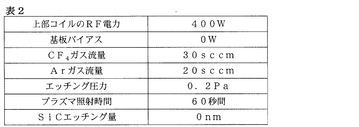
- Example 2 In order to suppress the etching amount of the silicon carbide (SiC) substrate by the plasma irradiation, the substrate processing was performed by replacing the plasma conditions by the inductively coupled plasma (ICP) etcher in the fourth step in Example 1 with the conditions in Table 2. .
- ICP inductively coupled plasma
- FIG. 5 is a surface observation view after the annealing treatment in this example.
- the RMS value was 1.6 nm
- the pretreatment by plasma irradiation before annealing treatment reduced surface roughness when high-temperature treatment of single crystal silicon carbide (SiC) was performed. It was found that there was an effect (FIG. 5).
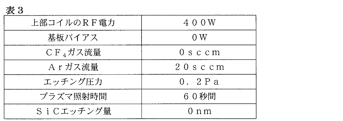
- Example 3 In order to evaluate the process gas flow rate ratio in the plasma irradiation, the substrate was processed by changing the plasma irradiation conditions by the inductively coupled plasma (ICP) etcher in the fourth step in Example 1 to the conditions in Table 3.
- ICP inductively coupled plasma
- FIG. 6 is a surface observation view after the annealing treatment in this example.
- the RMS value was 2.1 nm
- pretreatment by plasma irradiation before annealing treatment with argon (Ar) gas alone was performed using carbon tetrafluoride (CF 4 ) gas. It was found that the effect of reducing the surface roughness when single-crystal silicon carbide (SiC) was subjected to high-temperature treatment was smaller than that of the case of addition (FIG. 6).
- Example 4 Further, in order to evaluate the process gas flow ratio in plasma irradiation, the substrate was processed by changing the plasma irradiation condition by the inductively coupled plasma (ICP) etcher in the fourth step in Example 1 to the conditions in Table 4. .
- ICP inductively coupled plasma
- FIG. 7 is a surface observation view after the annealing process in this example.
- the RMS value was 0.9 nm
- the plasma irradiation before the annealing treatment with carbon tetrafluoride (CF 4 ) gas alone was a high temperature treatment of single crystal silicon carbide (SiC). It has been found that there is a great effect in reducing the surface roughness in the case of performing (Fig. 7).
- Example 5 in order to evaluate the effect of the case of performing high-temperature heat treatment in electron impact heating method in a vacuum atmosphere, the high temperature heat treatment of the fifth step, using the electron impact heating apparatus, 1 ⁇ 10 -3 Pa Substrate processing similar to that of Example 4 was performed in place of performing 1900 ° C. for 1 minute in the vacuum.
- FIG. 8 is a surface observation view after the annealing treatment in this example.
- the RMS value was 0.80 nm, and no minute pits were observed (FIG. 8). It has been found that plasma irradiation with carbon tetrafluoride (CF 4 ) gas alone is very effective in reducing surface roughness when high temperature treatment of single crystal silicon carbide (SiC) is performed.
- CF 4 carbon tetrafluoride
- Example 1 A silicon carbide (SiC) substrate was processed in the same manner as in Example 1 except that the fourth step (plasma irradiation) was not performed.
- FIG. 2 is a view of the surface after annealing in Comparative Example 1.
- the RMS value indicating the surface roughness was 6.6 nm, and step bunching, which is a large surface roughness, was observed.
- Example 2 A silicon carbide (SiC) substrate was processed in the same manner as in Example 5 except that the fourth step (plasma irradiation) was not performed.
- FIG. 3 is a surface observation view after the annealing treatment in Comparative Example 2. As can be seen from the AFM image shown in FIG. 3, in Comparative Example 2, the RMS value indicating surface roughness was suppressed to 1.57 nm, and step bunching was not observed, but 23 minute pits were observed.
- the single crystal silicon carbide (SiC) is subjected to a high temperature heat treatment (for example, annealing) before the single crystal
- a high temperature heat treatment for example, annealing
- surface roughness and pit formation can be reduced.
- This plasma irradiation is preferably performed using at least one of an inert gas such as argon (Ar) and a fluorine-based gas such as carbon tetrafluoride (CF 4 ).
- Example 6 Example 1 except that a single crystal silicon carbide (4H—SiC (0001)) substrate was used instead of a silicon carbide (4H—SiC (0001)) substrate having an epitaxial layer 2 formed by epitaxial growth as a substrate.
- the substrate processing was performed in the same manner. When compared with the substrate obtained by the substrate processing method in which the plasma irradiation in Step 4 was omitted, surface roughness could be suppressed.
- Example 7 Substrate processing was performed by the method of substrate processing method 2. When compared with a substrate obtained by a substrate processing method without plasma irradiation, surface roughness could be suppressed.
- the pretreatment by plasma irradiation is performed when high temperature heat treatment is performed on single crystal silicon carbide (SiC) or silicon carbide (SiC) epitaxially grown on a single crystal silicon carbide (SiC) substrate.
- SiC single crystal silicon carbide
- SiC silicon carbide
- the impurities injected into the single crystal silicon carbide (SiC) substrate are electrically activated by the high temperature heat treatment, before the high temperature heat treatment, the single crystal silicon carbide (SiC) substrate is By irradiating with plasma, formation of factors that deteriorate the flatness of the substrate surface such as step bunching and pits can be reduced.
- the substrate surface is treated so that the factors that deteriorate the flatness caused by the high-temperature heat treatment are not formed as much as possible, that is, the surface roughness caused by the high-temperature heat treatment is reduced.
- the silicon carbide (SiC) substrate is irradiated with plasma before the high temperature heat treatment.
- At least a substance other than the crystalline silicon carbide (SiC) substrate for example, an impurity such as silicon carbide oxide (SiOC) deposited or formed on the substrate
- an impurity such as silicon carbide oxide (SiOC) deposited or formed on the substrate
- Plasma irradiation is performed so as to remove a part. Even if a part of the crystalline silicon carbide (SiC) substrate is etched by the plasma irradiation (for example, Example 1) or not etched (for example, Examples 2 to 5), the substance as the impurity described above If at least a part of the surface can be removed, the cause of the surface roughness can be reduced, which leads to reduction in the occurrence of step bunching and pits.
- the present invention it is important to irradiate the substrate with plasma before the high-temperature heat treatment for the silicon carbide (SiC) substrate.
- the substrate is subjected to a treatment for suppressing generation of a factor that deteriorates the flatness caused by the high-temperature heat treatment.
- the present invention as described in Examples 2 to 5, even if the etching amount of the silicon carbide (SiC) substrate by plasma irradiation is made almost zero, the surface flatness of the substrate surface is deteriorated after the high-temperature heat treatment. It is suppressed.
- it is not essential to irradiate plasma to etch the substrate.
- the present invention is fundamentally different from the invention disclosed in Patent Document 3 in which the surface shape change such as step bunching already formed is removed by etching after the high temperature annealing process. Elements that cause bunching and pits are removed by plasma irradiation before heat treatment (annealing, etc.). That is, the present invention does not remove a region of a silicon carbide (SiC) substrate by etching using plasma. Therefore, even if the etching amount by plasma irradiation performed before the heat treatment is suppressed to 20 nm as in the first embodiment, step bunching and pit formation can be suppressed on the surface after the heat treatment. Further, as in Examples 2 to 5, even when the etching amount by the plasma irradiation is set to 0 nm, step bunching and pit formation can be suppressed on the surface after the heat treatment.
- SiC silicon carbide
Landscapes
- Drying Of Semiconductors (AREA)
- Crystals, And After-Treatments Of Crystals (AREA)
- Recrystallisation Techniques (AREA)
Abstract
Description
(基板処理方法1)
単結晶炭化ケイ素(SiC)の基板としては、単結晶炭化ケイ素(4H-SiC(0001))基板上に、p型SiCエピタキシャル層をCVDにて、10マイクロメートル成長させたサンプル基板を、RCA洗浄したものを用いる。従って、図1の初期ステップにおいて、p型SiCエピタキシャル層2が形成された単結晶炭化ケイ素(SiC)基板1を用意する。
なお、上記注入される不純物原子は、窒素(N)の他に、燐(P)、アルミニウム(Al)、またはホウ素(B)のいずれかであっても良い。
次に、本発明の基板処理方法の他の例を示す。
本実施形態は、上記基板処理方法1において、第1ステップ(バッファ層の形成)、第3ステップ(バッファー層の除去)の工程を省略したものである。
基板処理方法1の方法により、単結晶炭化ケイ素(SiC)基板の基板処理方法を行った。なお、第4ステップの誘導結合型プラズマ(ICP)エッチャーでのプラズマ照射は、アルゴン(Ar)ガスおよび、四フッ化炭素(CF4)ガスの混合ガスを用いて、表1の条件で行った。

原子間力顕微鏡(AFM:Atomic Force Microscopy)
NPX200M0001 セイコーインスツルメンツ株式会社製
観察ヘッド NPX200
コントローラー Nanopics 2100
ダンピングフォースモード(DFM)でスキャン
(一定の振幅で周期的に振動する探針を基板試料表面に近づけ、その振幅の減推量が一定のとなるようにカンチレバーと試料表面の距離を制御するモード)
プラズマ照射による炭化ケイ素(SiC)基板のエッチング量を抑えるために、実施例1における第4ステップの誘導結合型プラズマ(ICP)エッチャーによるプラズマ条件を表2の条件に代えて、基板処理を行った。
プラズマ照射におけるプロセスガス流量比を評価するために、実施例1における第4ステップの誘導結合型プラズマ(ICP)エッチャーによるプラズマ照射条件を表3の条件に代えて、基板の処理を行った。
更に、プラズマ照射におけるプロセスガス流量比を評価するために、実施例1における第4ステップの誘導結合型プラズマ(ICP)エッチャーによるプラズマ照射条件を表4の条件に代えて、基板の処理を行った。

次に、真空雰囲気における電子衝撃加熱方式で高温加熱処理を行った場合への効果を評価するために、第5ステップの高温加熱処理を、電子衝撃加熱装置を用いて、1×10⁻³Paの真空中にて1900℃、1分間行ったことに代えて、実施例4と同様の基板処理を行った。
第4ステップ(プラズマ照射)を行わなかったこと以外、実施例1と同様にして、炭化ケイ素(SiC)基板の処理を行った。
第4ステップ(プラズマ照射)を行わなかったこと以外、実施例5と同様にして、炭化ケイ素(SiC)基板の処理を行った。
基板としてエピタキシャル成長により形成されるエピタキシャル層2を有する炭化ケイ素(4H-SiC(0001))基板に代えて、単結晶炭化ケイ素(4H-SiC(0001))基板を用いた以外は、実施例1と同様に基板処理を行った。ステップ4のプラズマ照射を省略した基板処理方法で得られた基板と比較したところ、表面荒れを抑えることができた。
基板処理方法2の方法により、基板処理を行った。プラズマ照射を行わない基板処理方法で得られた基板と比較したところ、表面荒れを抑えることができた。
Claims (14)
- 不純物原子がイオン注入された結晶性炭化ケイ素(SiC)基板に、不活性ガスおよびフッ素系ガスの少なくとも一方を含むガスを用いてプラズマ照射を行う工程と、
前記プラズマ照射した結晶性炭化ケイ素(SiC)基板を高温加熱処理する工程と
を有することを特徴とする結晶性炭化ケイ素(SiC)基板の処理方法。 - 前記結晶性炭化ケイ素(SiC)基板は、エピタキシャル炭化ケイ素(SiC)結晶層を表面層として有することを特徴とする請求項1に記載の基板処理方法。
- 前記ガスは、アルゴンガス、四フッ化炭素ガス、またはアルゴンガスと四フッ化炭素ガスとの混合ガスのいずれかであることを特徴とする請求項1または2に記載の基板処理方法。
- 前記不純物原子が、窒素(N)、燐(P)、アルミニウム(Al)または、ホウ素(B)のいずれかであることを特徴とする請求項1ないし3のいずれかに記載の基板処理方法。
- 前記高温加熱処理が、高周波誘導加熱方式、電子衝撃加熱方式または、抵抗加熱方式の装置により行われることを特徴とする請求項1ないし4のいずれかに記載の基板処理方法。
- 所定の不純物原子がイオン注入された結晶性炭化ケイ素(SiC)基板を用意する工程と、
前記結晶性炭化ケイ素(SiC)基板に、不活性ガスおよびフッ素系ガスの少なくとも一方を含むガスを用いてプラズマ照射を行う工程と、
前記プラズマ照射した結晶性炭化ケイ素(SiC)基板を高温加熱処理する工程と
を有することを特徴とする結晶性炭化ケイ素(SiC)基板の製造方法。 - 前記結晶性炭化ケイ素(SiC)基板は、単結晶炭化ケイ素(SiC)基板であることを特徴とする請求項6に記載の結晶性炭化ケイ素(SiC)基板の製造方法。
- 前記単結晶炭化ケイ素(SiC)基板は、エピタキシャル炭化ケイ素(SiC)結晶層を表面層として有することを特徴とする請求項7に記載の結晶性炭化ケイ素(SiC)基板の製造方法。
- 前記ガスは、アルゴンガス、四フッ化炭素ガス、またはアルゴンガスと四フッ化炭素ガスとの混合ガスのいずれかであることを特徴とする請求項6ないし8のいずれかに記載の結晶性炭化ケイ素(SiC)基板の製造方法。
- 前記炭化ケイ素(SiC)基板を用意する工程は、前記結晶性炭化ケイ素(SiC)基板に対して、前記所定の不純物原子をイオン注入する工程を有することを特徴とする請求項6ないし9のいずれかに記載の結晶性炭化ケイ素(SiC)基板の製造方法。
- 前記結晶性炭化ケイ素(SiC)基板を用意する工程は、前記イオン注入する工程の前に、前記結晶性炭化ケイ素(SiC)基板の表面を含む一部分に対して犠牲酸化を行い、前記イオン注入に対するバッファ層を形成する工程をさらに有することを特徴とする請求項10に記載の炭化ケイ素(SiC)基板の製造方法。
- 前記イオン注入後に、前記バッファ層を除去する工程をさらに有することを特徴とする請求項11に記載の炭化ケイ素(SiC)基板の製造方法。
- 結晶性炭化ケイ素(SiC)基板の表面に存在する、該結晶性炭化ケイ素(SiC)基板以外の物質の少なくとも一部を除去するように、該結晶性炭化ケイ素(SiC)基板にプラズマ照射する工程と、
前記プラズマ照射した結晶性炭化ケイ素(SiC)基板を高温加熱処理する工程と
を有することを特徴とする結晶性炭化ケイ素(SiC)基板の処理方法。 - 所定の不純物原子がイオン注入された結晶性炭化ケイ素(SiC)基板を用意する工程と、
前記結晶性炭化ケイ素(SiC)基板の表面に存在する、該結晶性炭化ケイ素(SiC)基板以外の物質の少なくとも一部を除去するように、該結晶性炭化ケイ素(SiC)基板にプラズマ照射する工程と、
前記プラズマ照射した結晶性炭化ケイ素(SiC)基板を高温加熱処理する工程と
を有することを特徴とする結晶性炭化ケイ素(SiC)基板の製造方法。
Priority Applications (3)
| Application Number | Priority Date | Filing Date | Title |
|---|---|---|---|
| CN201080020525.1A CN102422396B (zh) | 2009-03-26 | 2010-03-16 | 基板处理方法和结晶性碳化硅(sic)基板的制造方法 |
| JP2011505987A JP5406279B2 (ja) | 2009-03-26 | 2010-03-16 | 基板処理方法および結晶性炭化ケイ素(SiC)基板の製造方法 |
| US13/234,594 US8187958B2 (en) | 2009-03-26 | 2011-09-16 | Substrate processing method and method of manufacturing crystalline silicon carbide (SIC) substrate |
Applications Claiming Priority (2)
| Application Number | Priority Date | Filing Date | Title |
|---|---|---|---|
| JP2009-076313 | 2009-03-26 | ||
| JP2009076313 | 2009-03-26 |
Related Child Applications (1)
| Application Number | Title | Priority Date | Filing Date |
|---|---|---|---|
| US13/234,594 Continuation US8187958B2 (en) | 2009-03-26 | 2011-09-16 | Substrate processing method and method of manufacturing crystalline silicon carbide (SIC) substrate |
Publications (1)
| Publication Number | Publication Date |
|---|---|
| WO2010110123A1 true WO2010110123A1 (ja) | 2010-09-30 |
Family
ID=42780815
Family Applications (1)
| Application Number | Title | Priority Date | Filing Date |
|---|---|---|---|
| PCT/JP2010/054437 Ceased WO2010110123A1 (ja) | 2009-03-26 | 2010-03-16 | 基板処理方法および結晶性炭化ケイ素(SiC)基板の製造方法 |
Country Status (4)
| Country | Link |
|---|---|
| US (1) | US8187958B2 (ja) |
| JP (1) | JP5406279B2 (ja) |
| CN (1) | CN102422396B (ja) |
| WO (1) | WO2010110123A1 (ja) |
Cited By (2)
| Publication number | Priority date | Publication date | Assignee | Title |
|---|---|---|---|---|
| EP2736067A4 (en) * | 2011-07-20 | 2015-07-08 | Sumitomo Electric Industries | Method for manufacturing semiconductor device |
| JP2018203611A (ja) * | 2017-05-31 | 2018-12-27 | インフィネオン テクノロジーズ アーゲーInfineon Technologies Ag | SiC表面の平坦化方法 |
Families Citing this family (16)
| Publication number | Priority date | Publication date | Assignee | Title |
|---|---|---|---|---|
| WO2012020556A1 (ja) | 2010-08-09 | 2012-02-16 | キヤノンアネルバ株式会社 | 基板加熱処理装置、基板加熱処理装置の温度制御方法、半導体デバイスの製造方法、基板加熱処理装置の温度制御プログラム及び記録媒体 |
| US8860040B2 (en) | 2012-09-11 | 2014-10-14 | Dow Corning Corporation | High voltage power semiconductor devices on SiC |
| US9018639B2 (en) | 2012-10-26 | 2015-04-28 | Dow Corning Corporation | Flat SiC semiconductor substrate |
| TWI600081B (zh) * | 2012-11-16 | 2017-09-21 | 東洋炭素股份有限公司 | Surface treatment method of single crystal silicon carbide substrate and single crystal silicon carbide substrate |
| US9738991B2 (en) | 2013-02-05 | 2017-08-22 | Dow Corning Corporation | Method for growing a SiC crystal by vapor deposition onto a seed crystal provided on a supporting shelf which permits thermal expansion |
| US9017804B2 (en) | 2013-02-05 | 2015-04-28 | Dow Corning Corporation | Method to reduce dislocations in SiC crystal growth |
| US9797064B2 (en) | 2013-02-05 | 2017-10-24 | Dow Corning Corporation | Method for growing a SiC crystal by vapor deposition onto a seed crystal provided on a support shelf which permits thermal expansion |
| US8940614B2 (en) | 2013-03-15 | 2015-01-27 | Dow Corning Corporation | SiC substrate with SiC epitaxial film |
| JP2014220322A (ja) * | 2013-05-07 | 2014-11-20 | 株式会社東芝 | 半導体装置の製造方法及び製造装置 |
| JP6248532B2 (ja) * | 2013-10-17 | 2017-12-20 | セイコーエプソン株式会社 | 3C−SiCエピタキシャル層の製造方法、3C−SiCエピタキシャル基板および半導体装置 |
| WO2015146162A1 (ja) | 2014-03-24 | 2015-10-01 | キヤノンアネルバ株式会社 | 半導体基板の熱処理方法及び熱処理装置 |
| US9279192B2 (en) | 2014-07-29 | 2016-03-08 | Dow Corning Corporation | Method for manufacturing SiC wafer fit for integration with power device manufacturing technology |
| CN112864006B (zh) * | 2021-01-11 | 2022-11-08 | 中国科学院上海微系统与信息技术研究所 | 一种半导体衬底的制备方法 |
| CN115206462B (zh) * | 2022-06-30 | 2026-03-13 | 哈尔滨工业大学 | 基于流动气体法模拟单晶碳化硅干氧热氧化工艺的方法 |
| CN116153778A (zh) * | 2022-12-15 | 2023-05-23 | 山东大学 | 一种去除碳化硅晶片表面金属的方法 |
| CN121075910A (zh) * | 2025-08-22 | 2025-12-05 | 湖南德智新材料股份有限公司 | 碳化硅表面处理方法 |
Citations (4)
| Publication number | Priority date | Publication date | Assignee | Title |
|---|---|---|---|---|
| JP2000036470A (ja) * | 1998-07-21 | 2000-02-02 | Fuji Electric Co Ltd | 炭化けい素半導体装置の製造方法 |
| JP2004363326A (ja) * | 2003-06-04 | 2004-12-24 | Fuji Electric Holdings Co Ltd | 炭化珪素半導体素子の製造方法 |
| JP2005260267A (ja) * | 2005-04-27 | 2005-09-22 | Fuji Electric Holdings Co Ltd | 炭化けい素半導体素子の製造方法 |
| JP2007273866A (ja) * | 2006-03-31 | 2007-10-18 | Tokyo Electron Ltd | エッチング方法、プラズマ処理装置、記憶媒体 |
Family Cites Families (7)
| Publication number | Priority date | Publication date | Assignee | Title |
|---|---|---|---|---|
| JP3733792B2 (ja) | 1999-07-22 | 2006-01-11 | 富士電機ホールディングス株式会社 | 炭化珪素半導体素子の製造方法 |
| US7473929B2 (en) | 2003-07-02 | 2009-01-06 | Panasonic Corporation | Semiconductor device and method for fabricating the same |
| JP3784393B2 (ja) | 2003-07-02 | 2006-06-07 | 松下電器産業株式会社 | 半導体装置及びその製造方法 |
| KR20060125700A (ko) * | 2004-02-06 | 2006-12-06 | 마츠시타 덴끼 산교 가부시키가이샤 | 탄화규소 반도체소자 및 그 제조방법 |
| US8177990B2 (en) | 2006-03-31 | 2012-05-15 | Tokyo Electron Limited | Etching method, plasma processing system and storage medium |
| JP2008112834A (ja) * | 2006-10-30 | 2008-05-15 | Sumitomo Electric Ind Ltd | 炭化ケイ素半導体装置の製造方法 |
| CN101652835B (zh) | 2007-04-20 | 2012-03-21 | 佳能安内华股份有限公司 | 具有碳化硅基板的半导体器件的退火方法和半导体器件 |
-
2010
- 2010-03-16 JP JP2011505987A patent/JP5406279B2/ja not_active Expired - Fee Related
- 2010-03-16 WO PCT/JP2010/054437 patent/WO2010110123A1/ja not_active Ceased
- 2010-03-16 CN CN201080020525.1A patent/CN102422396B/zh not_active Expired - Fee Related
-
2011
- 2011-09-16 US US13/234,594 patent/US8187958B2/en not_active Expired - Fee Related
Patent Citations (4)
| Publication number | Priority date | Publication date | Assignee | Title |
|---|---|---|---|---|
| JP2000036470A (ja) * | 1998-07-21 | 2000-02-02 | Fuji Electric Co Ltd | 炭化けい素半導体装置の製造方法 |
| JP2004363326A (ja) * | 2003-06-04 | 2004-12-24 | Fuji Electric Holdings Co Ltd | 炭化珪素半導体素子の製造方法 |
| JP2005260267A (ja) * | 2005-04-27 | 2005-09-22 | Fuji Electric Holdings Co Ltd | 炭化けい素半導体素子の製造方法 |
| JP2007273866A (ja) * | 2006-03-31 | 2007-10-18 | Tokyo Electron Ltd | エッチング方法、プラズマ処理装置、記憶媒体 |
Cited By (2)
| Publication number | Priority date | Publication date | Assignee | Title |
|---|---|---|---|---|
| EP2736067A4 (en) * | 2011-07-20 | 2015-07-08 | Sumitomo Electric Industries | Method for manufacturing semiconductor device |
| JP2018203611A (ja) * | 2017-05-31 | 2018-12-27 | インフィネオン テクノロジーズ アーゲーInfineon Technologies Ag | SiC表面の平坦化方法 |
Also Published As
| Publication number | Publication date |
|---|---|
| JPWO2010110123A1 (ja) | 2012-09-27 |
| CN102422396B (zh) | 2014-07-02 |
| JP5406279B2 (ja) | 2014-02-05 |
| US20120070968A1 (en) | 2012-03-22 |
| CN102422396A (zh) | 2012-04-18 |
| US8187958B2 (en) | 2012-05-29 |
Similar Documents
| Publication | Publication Date | Title |
|---|---|---|
| JP5406279B2 (ja) | 基板処理方法および結晶性炭化ケイ素(SiC)基板の製造方法 | |
| JP5896038B2 (ja) | ナノカーボン膜の作製方法 | |
| CN101652835B (zh) | 具有碳化硅基板的半导体器件的退火方法和半导体器件 | |
| TWI600081B (zh) | Surface treatment method of single crystal silicon carbide substrate and single crystal silicon carbide substrate | |
| JP5316612B2 (ja) | 炭化珪素半導体エピタキシャル基板の製造方法 | |
| CN106257619B (zh) | 碳化硅半导体装置的制造方法 | |
| JPWO2015199180A1 (ja) | ダイヤモンド基板の製造方法、ダイヤモンド基板、及び、ダイヤモンド複合基板 | |
| CN107344868B (zh) | 一种在SiC衬底上制备无缓冲层的单层石墨烯的方法 | |
| JP6108588B2 (ja) | 炭化珪素半導体素子の製造方法 | |
| JP2010157546A (ja) | 炭化珪素半導体装置の製造方法 | |
| JP4946264B2 (ja) | 炭化珪素半導体エピタキシャル基板の製造方法 | |
| JP2011035257A (ja) | 炭化珪素半導体装置の製造方法 | |
| WO2022158148A1 (ja) | エピタキシャルウェーハの製造方法 | |
| US9957639B2 (en) | Method for producing epitaxial silicon carbide wafer | |
| CN109023517B (zh) | 一种利用聚焦离子束技术消除单晶金刚石籽晶表面缺陷的方法 | |
| JP7035925B2 (ja) | エピタキシャルシリコンウェーハの製造方法およびエピタキシャルシリコンウェーハ | |
| JP5673107B2 (ja) | 炭化珪素半導体デバイスの作製方法 | |
| JP4511378B2 (ja) | SOI基板を用いた単結晶SiC層を形成する方法 | |
| JP6472016B2 (ja) | 炭化珪素半導体装置の製造方法 | |
| TW202548863A (zh) | 接合半導體基板及接合半導體基板之製造方法 | |
| CN115584478A (zh) | 一种低缺陷密度外延薄膜的制备方法 | |
| JP2011134983A (ja) | シリコン半導体基板の製造方法 | |
| JP2009302097A (ja) | 単結晶SiC基板の製造方法および単結晶SiC基板 | |
| JP2011138957A (ja) | シリコン半導体基板の製造方法 |
Legal Events
| Date | Code | Title | Description |
|---|---|---|---|
| WWE | Wipo information: entry into national phase |
Ref document number: 201080020525.1 Country of ref document: CN |
|
| 121 | Ep: the epo has been informed by wipo that ep was designated in this application |
Ref document number: 10755921 Country of ref document: EP Kind code of ref document: A1 |
|
| DPE1 | Request for preliminary examination filed after expiration of 19th month from priority date (pct application filed from 20040101) | ||
| WWE | Wipo information: entry into national phase |
Ref document number: 2011505987 Country of ref document: JP |
|
| NENP | Non-entry into the national phase |
Ref country code: DE |
|
| 122 | Ep: pct application non-entry in european phase |
Ref document number: 10755921 Country of ref document: EP Kind code of ref document: A1 |